US5295101A - Array block level redundancy with steering logic - Google Patents
Array block level redundancy with steering logic Download PDFInfo
- Publication number
- US5295101A US5295101A US07/829,124 US82912492A US5295101A US 5295101 A US5295101 A US 5295101A US 82912492 A US82912492 A US 82912492A US 5295101 A US5295101 A US 5295101A
- Authority
- US
- United States
- Prior art keywords
- memory cells
- block
- memory
- sub
- defective
- Prior art date
- Legal status (The legal status is an assumption and is not a legal conclusion. Google has not performed a legal analysis and makes no representation as to the accuracy of the status listed.)
- Expired - Lifetime
Links
Images


Classifications
-
- G—PHYSICS
- G11—INFORMATION STORAGE
- G11C—STATIC STORES
- G11C29/00—Checking stores for correct operation ; Subsequent repair; Testing stores during standby or offline operation
- G11C29/70—Masking faults in memories by using spares or by reconfiguring
- G11C29/78—Masking faults in memories by using spares or by reconfiguring using programmable devices
- G11C29/80—Masking faults in memories by using spares or by reconfiguring using programmable devices with improved layout
- G11C29/81—Masking faults in memories by using spares or by reconfiguring using programmable devices with improved layout using a hierarchical redundancy scheme
-
- G—PHYSICS
- G11—INFORMATION STORAGE
- G11C—STATIC STORES
- G11C29/00—Checking stores for correct operation ; Subsequent repair; Testing stores during standby or offline operation
- G11C29/70—Masking faults in memories by using spares or by reconfiguring
- G11C29/88—Masking faults in memories by using spares or by reconfiguring with partially good memories
-
- G—PHYSICS
- G06—COMPUTING; CALCULATING OR COUNTING
- G06F—ELECTRIC DIGITAL DATA PROCESSING
- G06F11/00—Error detection; Error correction; Monitoring
- G06F11/07—Responding to the occurrence of a fault, e.g. fault tolerance
- G06F11/08—Error detection or correction by redundancy in data representation, e.g. by using checking codes
- G06F11/10—Adding special bits or symbols to the coded information, e.g. parity check, casting out 9's or 11's
- G06F11/1008—Adding special bits or symbols to the coded information, e.g. parity check, casting out 9's or 11's in individual solid state devices
Definitions
- the present invention relates to the field of semiconductor memory devices and, more particularly, to devices which include repair circuitry for eliminating defects in memory devices.
- an array of memory cells In the fabrication of semiconductor memory devices it is common for an array of memory cells to include one or more defects which prevent the proper performance of the memory circuit. If a type of defect occurs systematically it can often be causally analyzed and designed out. Other defects which are generally not systematic include short circuits between adjacent columns and open circuits within individual columns of memory cells. For analysis purposes the distribution of such defects in a memory device, as well as the distribution of the number of defects among a given production lot, may be considered random so that the yield of good devices in a lot can be modelled according to a Poisson distribution function. Typically, over the period of time that a particular device or family of devices is being produced in a given manufacturing facility the product yield can be improved by removing causes, e.g., particulate matter, of the above-mentioned random defects.
- redundancy schemes have been introduced to reduce the effect these defects have on device yield.
- the redundancy schemes normally consist of a few extra rows and columns of memory cells that are placed within the memory array to replace defective rows and columns of memory cells. In theory, these extra rows and columns of memory cells should maximize the yield of a production lot. Practically, however, many potentially functional devices must be rejected because the number of available redundant elements on the chip prove to be insufficient to meet the repair needs of the device.
- the described embodiments of the present invention provide a circuit and method for employing a second level of redundancy that allows the use of memory allocated for parity bit storage in a DRAM part to be used as redundancy to yield a functional DRAM.
- the second level of redundancy can be used once the first level of redundancy, having standard redundant elements, is exhausted.
- the embodiments described provide this function for dynamic random access memories (DRAMs) but are applicable to other integrated circuits.
- a second level of redundancy is used to yield a functional 16 Mb DRAM part from an intended 18 Mb DRAM part containing up to 2 Mb of defective, irreparable memory locations. Without this system, many salvageable 18 Mb DRAM parts would have to be rejected due to standard redundant element exhaustion. Also, it is important to note that part rejection due to an insufficient number of standard redundant elements is more common with fabrication processes that are not yet mature. It follows that the device yield can be greatly improved with this scheme at the early stages of process development.
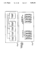
- FIG. 1 is a plan view of a memory device which may incorporate the invention.
- FIG. 2 illustrates the general layout of a logical data block in the device of FIG. 1.
- FIG. 3 illustrates in block diagram form a standard first level redundancy scheme.
- FIG. 4 illustrates in block diagram form one redundant row line for an array block of memory.
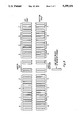
- FIG. 5 illustrates in block diagram form a standard first level row redundancy scheme.
- FIG. 6 illustrates in block diagram form a second level redundancy scheme according to the invention.
- FIG. 7 illustrates in block diagram form the second level redundancy system as it relates to the standard first level row redundancy scheme.
- FIG. 8 illustrates in block diagram form the steering system according to the invention.
- FIG. 9 illustrates in block diagram form the conceptual partitioning of the total chip memory into sections of memory.
- FIG. 1 illustrates a semiconductor memory device with which the invention may be practiced.
- This exemplary device 10 is a DRAM of the so-called 16 Megabit (Mb) density, but virtually contains 18 megabits of storage capability, including 2 megabits dedicated to parity bit storage.
- Device 10 has (2 18 ) ⁇ 72 or 18,874,368 one-transistor storage cells arranged in rows and columns.
- the device is partitioned into four identical logical data blocks 12, individually designated 12a, 12b, 12c and 12d.
- Each block 12 is of the four and one half (4.5) megabit size, comprising 4,718,592 memory cells arranged in an array of 4,608 rows R and 1,024 columns C.
- each data block 12 is partitioned into eighteen sub-blocks 14. Within each sub-block 14 there are 256 row or word lines R and 256 column select lines Y s . A row line is selectable based on row address information input to a one of 18 row decoder stage 16 and a one of 256 row decoder stage 18. In each data block 12 column address decoders 20 turn on a select line Y s to control read/write data transfer for four columns each having 256 physical rows.
- the Device 10 includes a first level redundancy system for overcoming defects in the logical data blocks 12.
- the first level redundancy system shown in FIG. 3, provides a redundant element which may replace in function any one of the regular elements.
- This first level redundancy system lends itself to replacement of a defective column or row with any of multiple identical redundant columns or rows.
- Such a redundancy system is common on many modern DRAM circuits.
- one row redundant element may be used to replace one defective row in an array block, as shown in FIG. 4.
- each sub-block 14 includes multiple redundant row lines, usually four, in addition to the regular 256 rows as shown in FIG. 5. All four redundancy rows in FIG. 5 are located on the right side of the 256K block. Each of these redundant wordlines is capable of replacing any of the faulty rows within the same block.
- a second level redundancy system is added to the first level redundancy system of device 10 that can be used once the first level redundancy system has been exhausted.
- FIG. 6 shows the basic concept of this second level redundancy system in which an entire block A of memory elements are replaced by memory block B.
- FIG. 7 shows the second level redundancy system as it relates to the first level redundancy system.
- Four array blocks and their associated redundant rows form the second level redundancy replacement unit or section.
- the choice of four adjacent array blocks to form the replacement memory section here results from row path decoding access patterns inherent in the preferred embodiment. This allows simplification of the section replacement logic. It is, however, largely an arbitrary choice and it does not indicate a restriction on the second level redundancy system.
- FIG. 8 shows the associated steering system that redirects the replacement section I/O to the appropriate DQ (input/output) pin.
- the REGULAR SECTION shown in FIG. 7 is an example of one of MEMORY SECTION A-D of FIG. 8.
- the steering system in this preferred embodiment uses signals FA, FB, FC and FD as defective section indicator signals.
- One method of generating these signals is via fuse logic implementation (not shown). That is, if a section is defective, a corresponding fuse structure is blown via laser and a logic high level (“1") is the resulting boolean equivalent of the logic circuit implementation. Similarly, if a section is fully functional, then its corresponding fuse structure is left intact and the resulting boolean equivalent is a logic low level ("0").
- one of FA-FD will go active high and DLR will be directed to the corresponding DL2A-DL2D line.
- the specific product that has provided motivation for the above-mentioned scheme is the 1M ⁇ 18/2M ⁇ 9 DRAM.
- This set of devices stores parity bits associated with the 8-bit words.
- the array block organization of this device allows for 2 Mb of its 18 Mb of memory to replace in function 2 Mb of defective memory.
- the resulting device contains 16 Mb of functional memory and is then organized as 1M ⁇ 16/2M ⁇ 8.
- This device stores no parity bits.
- the portion of the 1M ⁇ 18/2M ⁇ 9 that is used to functionally replace the defective memory portion(s) is the part of memory allocated for parity bit storage in the fully functional 1M ⁇ 18/2M ⁇ 9 part.
- FIG. 9 illustrates the conceptual partitioning of the total chip memory into sections of memory. Each section contains four memory array blocks or 1 Mb of memory and is indicated by brackets.
- the parity sections are labelled on the diagram as parity top and parity bottom. These two sections serve as replacement sections. These parity sections provide the second level of redundancy as each is able to wholly replace in function any one of the other sections labelled 0-7.
- Each section has a fuse circuit associated with it (not shown) where a blown fuse indicates that the section is defective.
- a section is considered defective if any array block within that section contains a defect that cannot be repaired using the existing first (standard) level redundant elements.
- a defective section is made to resemble a fully functional section in its precharge cycle. That is, the sensing activation circuits accessing the defective section operate to maintain bitline equalization and to suppress wordline rise. Thus, power is not wasted on a memory section that will be effectively replaced.
- the other main functional part needed to implement this preferred embodiment is the steering logic, previously discussed and shown in FIG. 8.
- This is the logic circuit that acts to multiplex between data from the defective section and data from the replacing section. This operation is done at the I/O level and it involves using the defective section indicator fuses to steer the data from the replacing section to the appropriate DQ(s) previously associated with the defective section(s).
- this preferred embodiment allows the use of 2 Mb of memory allocated for parity bit storage in an 18 Mb DRAM part to be used as redundancy in yielding a 16 Mb DRAM. Without this system, many salvageable 18 Mb DRAM parts would have to be rejected due to standard redundant element exhaustion. Also, it is important to note that part rejection due to an insufficient number of standard redundant elements is more common with fabrication processes that are not yet mature. It follows that the device yield can be greatly improved with this scheme at the early stages of process development.
Landscapes
- Dram (AREA)
- For Increasing The Reliability Of Semiconductor Memories (AREA)
Abstract
Description
Claims (17)
Priority Applications (2)
| Application Number | Priority Date | Filing Date | Title |
|---|---|---|---|
| US07/829,124 US5295101A (en) | 1992-01-31 | 1992-01-31 | Array block level redundancy with steering logic |
| JP5014103A JPH0612893A (en) | 1992-01-31 | 1993-01-29 | Memory device having redundancy at array block level and method for correcting defect thereof |
Applications Claiming Priority (1)
| Application Number | Priority Date | Filing Date | Title |
|---|---|---|---|
| US07/829,124 US5295101A (en) | 1992-01-31 | 1992-01-31 | Array block level redundancy with steering logic |
Publications (1)
| Publication Number | Publication Date |
|---|---|
| US5295101A true US5295101A (en) | 1994-03-15 |
Family
ID=25253591
Family Applications (1)
| Application Number | Title | Priority Date | Filing Date |
|---|---|---|---|
| US07/829,124 Expired - Lifetime US5295101A (en) | 1992-01-31 | 1992-01-31 | Array block level redundancy with steering logic |
Country Status (2)
| Country | Link |
|---|---|
| US (1) | US5295101A (en) |
| JP (1) | JPH0612893A (en) |
Cited By (38)
| Publication number | Priority date | Publication date | Assignee | Title |
|---|---|---|---|---|
| US5446692A (en) * | 1992-02-14 | 1995-08-29 | Mitsubishi Denki Kabushiki Kaisha | Semiconductor memory device having redundancy memory cells shared among memory blocks |
| US5469389A (en) * | 1993-03-31 | 1995-11-21 | Sgs-Thomson Microelectronics S.R.L. | Semiconductor memory with memory matrix comprising redundancy cell columns associated with single matrix sectors |
| US5475648A (en) * | 1992-02-07 | 1995-12-12 | Matsushita Electric Industrial Co., Ltd. | Redundancy semiconductor memory device which utilizes spare memory cells from a plurality of different memory blocks, and utilizes the same decode lines for both the primary and spare memory cells |
| EP0691617A2 (en) * | 1994-07-05 | 1996-01-10 | Monolithic System Technology, Inc. | Directional asymmetric signal swing bus system for circuit module architecture |
| US5491664A (en) * | 1993-09-27 | 1996-02-13 | Cypress Semiconductor Corporation | Flexibilitiy for column redundancy in a divided array architecture |
| US5584002A (en) * | 1993-02-22 | 1996-12-10 | International Business Machines Corporation | Cache remapping using synonym classes |
| US5600602A (en) * | 1995-04-05 | 1997-02-04 | Micron Technology, Inc. | Hierarchical memory array structure having electrically isolated bit lines for temporary data storage |
| US5621690A (en) * | 1995-04-28 | 1997-04-15 | Intel Corporation | Nonvolatile memory blocking architecture and redundancy |
| US5666312A (en) * | 1994-11-23 | 1997-09-09 | Sony Corporation Of Japan | Column redundancy scheme for a random access memory incorporating multiplexers and demultiplexers for replacing defective columns in any memory array |
| US5706234A (en) * | 1994-04-29 | 1998-01-06 | Texas Instruments Incorporated | Testing and repair of wide I/O semiconductor memory devices designed for testing |
| US5734620A (en) * | 1995-04-05 | 1998-03-31 | Micron Technology, Inc. | Hierarchical memory array structure with redundant components having electrically isolated bit lines |
| US5742547A (en) * | 1995-08-22 | 1998-04-21 | Samsung Electronics Co., Ltd. | Circuits for block redundancy repair of integrated circuit memory devices |
| US5748872A (en) * | 1994-03-22 | 1998-05-05 | Norman; Richard S. | Direct replacement cell fault tolerant architecture |
| US5761145A (en) * | 1994-10-19 | 1998-06-02 | Micron Technology, Inc. | Efficient method for obtaining usable parts from a partially good memory integrated circuit |
| US5822256A (en) * | 1994-09-06 | 1998-10-13 | Intel Corporation | Method and circuitry for usage of partially functional nonvolatile memory |
| US5831913A (en) * | 1997-03-31 | 1998-11-03 | International Business Machines Corporation | Method of making a memory fault-tolerant using a variable size redundancy replacement configuration |
| US5831914A (en) * | 1997-03-31 | 1998-11-03 | International Business Machines Corporation | Variable size redundancy replacement architecture to make a memory fault-tolerant |
| US5881003A (en) * | 1997-07-16 | 1999-03-09 | International Business Machines Corporation | Method of making a memory device fault tolerant using a variable domain redundancy replacement configuration |
| US5946257A (en) * | 1996-07-24 | 1999-08-31 | Micron Technology, Inc. | Selective power distribution circuit for an integrated circuit |
| US5970000A (en) * | 1998-02-02 | 1999-10-19 | International Business Machines Corporation | Repairable semiconductor integrated circuit memory by selective assignment of groups of redundancy elements to domains |
| US5978291A (en) * | 1998-09-30 | 1999-11-02 | International Business Machines Corporation | Sub-block redundancy replacement for a giga-bit scale DRAM |
| US5978931A (en) * | 1997-07-16 | 1999-11-02 | International Business Machines Corporation | Variable domain redundancy replacement configuration for a memory device |
| US6038179A (en) * | 1999-01-04 | 2000-03-14 | International Business Machines Corp. | Multiple repair size redundancy |
| US6104646A (en) * | 1997-08-28 | 2000-08-15 | Kabushiki Kaisha Toshiba | Semiconductor memory device having redundancy circuit with high rescue efficiency |
| US20040015735A1 (en) * | 1994-03-22 | 2004-01-22 | Norman Richard S. | Fault tolerant cell array architecture |
| US20040017703A1 (en) * | 2002-07-29 | 2004-01-29 | Renesas Technology Corp. | Semiconductor memory device |
| US20040245626A1 (en) * | 2003-03-27 | 2004-12-09 | Matsushita Electric Industrial Co., Ltd. | Semiconductor device, system device using it, and manufacturing method of a semiconductor device |
| US20050002243A1 (en) * | 2003-07-02 | 2005-01-06 | Mohr Christian N. | Reduced power redundancy address decoder and comparison circuit |
| EP1622167A2 (en) | 2004-07-30 | 2006-02-01 | Fujitsu Limited | Cache memory and processor and their production methods |
| US20060221729A1 (en) * | 2005-04-04 | 2006-10-05 | Kabushiki Kaisha Toshiba | Semiconductor memory device |
| US20070083697A1 (en) * | 2005-10-07 | 2007-04-12 | Microsoft Corporation | Flash memory management |
| US20070133322A1 (en) * | 2005-09-30 | 2007-06-14 | Manfred Proell | Memory and method for improving the reliability of a memory having a used memory region and an unused memory region |
| KR100821579B1 (en) | 2006-09-15 | 2008-04-15 | 주식회사 하이닉스반도체 | Semiconductor Memory Apparatus and Method for Testing the same |
| US20090222689A1 (en) * | 2006-08-24 | 2009-09-03 | Vipul Patel | Memory device internal parameter reliability |
| US20090303815A1 (en) * | 2008-06-06 | 2009-12-10 | Lizhen Yu | Apparatus for redundancy reconfiguration of faculty memories |
| US8341503B1 (en) * | 2006-11-30 | 2012-12-25 | Marvell International Ltd. | Methods and systems for storing data in memory using zoning |
| US8451668B1 (en) | 2011-12-01 | 2013-05-28 | International Business Machines Corporation | Implementing column redundancy steering for memories with wordline repowering |
| US11860885B2 (en) * | 2017-08-30 | 2024-01-02 | Gsi Technology Inc. | One by one selection of items of a set |
Citations (3)
| Publication number | Priority date | Publication date | Assignee | Title |
|---|---|---|---|---|
| US5033024A (en) * | 1989-01-06 | 1991-07-16 | U.S. Philips Corp. | Matrix memory with redundancy and minimizes delay |
| US5060197A (en) * | 1989-12-30 | 1991-10-22 | Samsung Electronics Co., Ltd | Static random access memory with redundancy |
| US5126973A (en) * | 1990-02-14 | 1992-06-30 | Texas Instruments Incorporated | Redundancy scheme for eliminating defects in a memory device |
-
1992
- 1992-01-31 US US07/829,124 patent/US5295101A/en not_active Expired - Lifetime
-
1993
- 1993-01-29 JP JP5014103A patent/JPH0612893A/en active Pending
Patent Citations (3)
| Publication number | Priority date | Publication date | Assignee | Title |
|---|---|---|---|---|
| US5033024A (en) * | 1989-01-06 | 1991-07-16 | U.S. Philips Corp. | Matrix memory with redundancy and minimizes delay |
| US5060197A (en) * | 1989-12-30 | 1991-10-22 | Samsung Electronics Co., Ltd | Static random access memory with redundancy |
| US5126973A (en) * | 1990-02-14 | 1992-06-30 | Texas Instruments Incorporated | Redundancy scheme for eliminating defects in a memory device |
Cited By (62)
| Publication number | Priority date | Publication date | Assignee | Title |
|---|---|---|---|---|
| US5475648A (en) * | 1992-02-07 | 1995-12-12 | Matsushita Electric Industrial Co., Ltd. | Redundancy semiconductor memory device which utilizes spare memory cells from a plurality of different memory blocks, and utilizes the same decode lines for both the primary and spare memory cells |
| US5446692A (en) * | 1992-02-14 | 1995-08-29 | Mitsubishi Denki Kabushiki Kaisha | Semiconductor memory device having redundancy memory cells shared among memory blocks |
| US5584002A (en) * | 1993-02-22 | 1996-12-10 | International Business Machines Corporation | Cache remapping using synonym classes |
| US5469389A (en) * | 1993-03-31 | 1995-11-21 | Sgs-Thomson Microelectronics S.R.L. | Semiconductor memory with memory matrix comprising redundancy cell columns associated with single matrix sectors |
| US5491664A (en) * | 1993-09-27 | 1996-02-13 | Cypress Semiconductor Corporation | Flexibilitiy for column redundancy in a divided array architecture |
| US20040015735A1 (en) * | 1994-03-22 | 2004-01-22 | Norman Richard S. | Fault tolerant cell array architecture |
| US7299377B2 (en) * | 1994-03-22 | 2007-11-20 | Richard S. Norman | Fault tolerant cell array architecture |
| US5748872A (en) * | 1994-03-22 | 1998-05-05 | Norman; Richard S. | Direct replacement cell fault tolerant architecture |
| US5706234A (en) * | 1994-04-29 | 1998-01-06 | Texas Instruments Incorporated | Testing and repair of wide I/O semiconductor memory devices designed for testing |
| EP0691617A3 (en) * | 1994-07-05 | 1996-09-11 | Monolithic System Tech Inc | Directional asymmetric signal swing bus system for circuit module architecture |
| EP0691617A2 (en) * | 1994-07-05 | 1996-01-10 | Monolithic System Technology, Inc. | Directional asymmetric signal swing bus system for circuit module architecture |
| US5822256A (en) * | 1994-09-06 | 1998-10-13 | Intel Corporation | Method and circuitry for usage of partially functional nonvolatile memory |
| US5761145A (en) * | 1994-10-19 | 1998-06-02 | Micron Technology, Inc. | Efficient method for obtaining usable parts from a partially good memory integrated circuit |
| US5970008A (en) * | 1994-10-19 | 1999-10-19 | Micron Technology, Inc. | Efficient method for obtaining usable parts from a partially good memory integrated circuit |
| US6097647A (en) * | 1994-10-19 | 2000-08-01 | Micron Technology, Inc. | Efficient method for obtaining usable parts from a partially good memory integrated circuit |
| US5666312A (en) * | 1994-11-23 | 1997-09-09 | Sony Corporation Of Japan | Column redundancy scheme for a random access memory incorporating multiplexers and demultiplexers for replacing defective columns in any memory array |
| US5724301A (en) * | 1995-04-05 | 1998-03-03 | Micron Technology, Inc. | Hierarchical memory array structure having electrically isolated bit lines for temporary data storage |
| US5734620A (en) * | 1995-04-05 | 1998-03-31 | Micron Technology, Inc. | Hierarchical memory array structure with redundant components having electrically isolated bit lines |
| US5600602A (en) * | 1995-04-05 | 1997-02-04 | Micron Technology, Inc. | Hierarchical memory array structure having electrically isolated bit lines for temporary data storage |
| US5621690A (en) * | 1995-04-28 | 1997-04-15 | Intel Corporation | Nonvolatile memory blocking architecture and redundancy |
| US5742547A (en) * | 1995-08-22 | 1998-04-21 | Samsung Electronics Co., Ltd. | Circuits for block redundancy repair of integrated circuit memory devices |
| US6356498B1 (en) | 1996-07-24 | 2002-03-12 | Micron Technology, Inc. | Selective power distribution circuit for an integrated circuit |
| US6078540A (en) * | 1996-07-24 | 2000-06-20 | Micron Technology, Inc. | Selective power distribution circuit for an integrated circuit |
| US5946257A (en) * | 1996-07-24 | 1999-08-31 | Micron Technology, Inc. | Selective power distribution circuit for an integrated circuit |
| US5831914A (en) * | 1997-03-31 | 1998-11-03 | International Business Machines Corporation | Variable size redundancy replacement architecture to make a memory fault-tolerant |
| US5940335A (en) * | 1997-03-31 | 1999-08-17 | International Business Machines Corporation | Prioritizing the repair of faults in a semiconductor memory device |
| US5831913A (en) * | 1997-03-31 | 1998-11-03 | International Business Machines Corporation | Method of making a memory fault-tolerant using a variable size redundancy replacement configuration |
| US5978931A (en) * | 1997-07-16 | 1999-11-02 | International Business Machines Corporation | Variable domain redundancy replacement configuration for a memory device |
| US5881003A (en) * | 1997-07-16 | 1999-03-09 | International Business Machines Corporation | Method of making a memory device fault tolerant using a variable domain redundancy replacement configuration |
| US6104646A (en) * | 1997-08-28 | 2000-08-15 | Kabushiki Kaisha Toshiba | Semiconductor memory device having redundancy circuit with high rescue efficiency |
| US5970000A (en) * | 1998-02-02 | 1999-10-19 | International Business Machines Corporation | Repairable semiconductor integrated circuit memory by selective assignment of groups of redundancy elements to domains |
| US5978291A (en) * | 1998-09-30 | 1999-11-02 | International Business Machines Corporation | Sub-block redundancy replacement for a giga-bit scale DRAM |
| US6038179A (en) * | 1999-01-04 | 2000-03-14 | International Business Machines Corp. | Multiple repair size redundancy |
| US6901015B2 (en) * | 2002-07-29 | 2005-05-31 | Renesas Technology Corp. | Semiconductor memory device |
| US20040017703A1 (en) * | 2002-07-29 | 2004-01-29 | Renesas Technology Corp. | Semiconductor memory device |
| US7126836B2 (en) | 2003-03-27 | 2006-10-24 | Matsushita Electric Industrial Co., Ltd. | Semiconductor device, system device using it, and manufacturing method of a semiconductor device |
| US20040245626A1 (en) * | 2003-03-27 | 2004-12-09 | Matsushita Electric Industrial Co., Ltd. | Semiconductor device, system device using it, and manufacturing method of a semiconductor device |
| US20050002243A1 (en) * | 2003-07-02 | 2005-01-06 | Mohr Christian N. | Reduced power redundancy address decoder and comparison circuit |
| US6868019B2 (en) | 2003-07-02 | 2005-03-15 | Micron Technology, Inc. | Reduced power redundancy address decoder and comparison circuit |
| US20050099861A1 (en) * | 2003-07-02 | 2005-05-12 | Mohr Christian N. | Reduced power redundancy address decoder and comparison circuit |
| US7145817B2 (en) | 2003-07-02 | 2006-12-05 | Micron Technology, Inc. | Reduced power redundancy address decoder and comparison circuit |
| US8694838B2 (en) | 2004-07-30 | 2014-04-08 | Fujitsu Limited | Cache memory, processor, and production methods for cache memory and processor |
| JP2006048170A (en) * | 2004-07-30 | 2006-02-16 | Fujitsu Ltd | Cache memory, processor, method for manufacturing cache memory and method for manufacturing processor |
| US20060026454A1 (en) * | 2004-07-30 | 2006-02-02 | Fujitsu Limited | Cache memory, processor, and production methods for cache memory and processor |
| US7783939B2 (en) * | 2004-07-30 | 2010-08-24 | Fujitsu Limited | Cache memory, processor, and production methods for cache memory and processor |
| JP4676723B2 (en) * | 2004-07-30 | 2011-04-27 | 富士通株式会社 | Cache memory, processor, cache memory manufacturing method, processor manufacturing method |
| US20100313081A1 (en) * | 2004-07-30 | 2010-12-09 | Fujitsu Limited | Cache memory, processor, and production methods for cache memory and processor |
| EP1622167A2 (en) | 2004-07-30 | 2006-02-01 | Fujitsu Limited | Cache memory and processor and their production methods |
| US20060221729A1 (en) * | 2005-04-04 | 2006-10-05 | Kabushiki Kaisha Toshiba | Semiconductor memory device |
| US7263010B2 (en) * | 2005-04-04 | 2007-08-28 | Kabushiki Kaisha Toshiba | Semiconductor memory device with test circuit |
| US20070133322A1 (en) * | 2005-09-30 | 2007-06-14 | Manfred Proell | Memory and method for improving the reliability of a memory having a used memory region and an unused memory region |
| US7512023B2 (en) * | 2005-09-30 | 2009-03-31 | Qimonda Ag | Memory and method for improving the reliability of a memory having a used memory region and an unused memory region |
| US20070083697A1 (en) * | 2005-10-07 | 2007-04-12 | Microsoft Corporation | Flash memory management |
| US7818611B2 (en) * | 2006-08-24 | 2010-10-19 | Micron Technology, Inc. | Memory device internal parameter reliability |
| US20090222689A1 (en) * | 2006-08-24 | 2009-09-03 | Vipul Patel | Memory device internal parameter reliability |
| KR100821579B1 (en) | 2006-09-15 | 2008-04-15 | 주식회사 하이닉스반도체 | Semiconductor Memory Apparatus and Method for Testing the same |
| US8341503B1 (en) * | 2006-11-30 | 2012-12-25 | Marvell International Ltd. | Methods and systems for storing data in memory using zoning |
| US8799724B1 (en) | 2006-11-30 | 2014-08-05 | Marvell International Ltd. | Methods and systems for storing data in memory using zoning |
| US7783940B2 (en) * | 2008-06-06 | 2010-08-24 | Syntest Technologies, Inc. | Apparatus for redundancy reconfiguration of faculty memories |
| US20090303815A1 (en) * | 2008-06-06 | 2009-12-10 | Lizhen Yu | Apparatus for redundancy reconfiguration of faculty memories |
| US8451668B1 (en) | 2011-12-01 | 2013-05-28 | International Business Machines Corporation | Implementing column redundancy steering for memories with wordline repowering |
| US11860885B2 (en) * | 2017-08-30 | 2024-01-02 | Gsi Technology Inc. | One by one selection of items of a set |
Also Published As
| Publication number | Publication date |
|---|---|
| JPH0612893A (en) | 1994-01-21 |
Similar Documents
| Publication | Publication Date | Title |
|---|---|---|
| US5295101A (en) | Array block level redundancy with steering logic | |
| US5126973A (en) | Redundancy scheme for eliminating defects in a memory device | |
| US5940335A (en) | Prioritizing the repair of faults in a semiconductor memory device | |
| US6199177B1 (en) | Device and method for repairing a semiconductor memory | |
| US6910152B2 (en) | Device and method for repairing a semiconductor memory | |
| KR100392557B1 (en) | Semiconductor device, computer system and access method | |
| EP0313040B1 (en) | Erasable programmable read only memory device | |
| US6434066B1 (en) | Device and method for repairing a semiconductor memory | |
| US5270975A (en) | Memory device having a non-uniform redundancy decoder arrangement | |
| US5831913A (en) | Method of making a memory fault-tolerant using a variable size redundancy replacement configuration | |
| US6307795B1 (en) | Semiconductor memory having multiple redundant columns with offset segmentation boundaries | |
| JP5033887B2 (en) | Method and apparatus for sharing redundant circuits between memory arrays in a semiconductor memory device | |
| US5495447A (en) | Method and apparatus using mapped redundancy to perform multiple large block memory array repair | |
| JP3254432B2 (en) | Highly reliable semiconductor integrated circuit memory by selective assignment of redundant element groups to domains | |
| KR100409114B1 (en) | Integrated semiconductor memory device | |
| US6426901B2 (en) | Logic consolidated semiconductor memory device having memory circuit and logic circuit integrated in the same chip | |
| EP0465808B1 (en) | Variable size set associative DRAM redundancy scheme | |
| JP2004062999A (en) | Semiconductor memory device | |
| EP0869440B1 (en) | Fault-tolerant memories | |
| EP1408513A1 (en) | Carry decoder for a memory | |
| WO1998028746A1 (en) | Redundancy for wide hierarchical i/o organizations | |
| JPH09106697A (en) | Semiconductor memory device | |
| KR20010106993A (en) | Semiconductor memory device with self block repair function |
Legal Events
| Date | Code | Title | Description |
|---|---|---|---|
| AS | Assignment |
Owner name: TEXAS INSTRUMENTS INCORPORATED A CORPORATION OF Free format text: ASSIGNMENT OF ASSIGNORS INTEREST.;ASSIGNOR:STEPHENS, MICHAEL C., JR.;REEL/FRAME:006000/0390 Effective date: 19920131 |
|
| AS | Assignment |
Owner name: TEXAS INSTRUMENTS INCORPORATED, TEXAS Free format text: ASSIGNMENT OF ASSIGNORS INTEREST.;ASSIGNORS:STEPHENS, MICHAEL C., JR.;TSAI, TERRY;PIEJKO, ARTHUR R.;REEL/FRAME:006085/0764;SIGNING DATES FROM 19920312 TO 19920320 Owner name: TEXAS INSTRUMENTS INCORPORATED, TEXAS Free format text: ASSIGNMENT OF ASSIGNORS INTEREST.;ASSIGNORS:SMITH, SCOTT E.;PILCH, CHARLES J., JR.;LE, DUY-LOAN T.;REEL/FRAME:006085/0767 Effective date: 19920312 |
|
| STCF | Information on status: patent grant |
Free format text: PATENTED CASE |
|
| REMI | Maintenance fee reminder mailed | ||
| FPAY | Fee payment |
Year of fee payment: 4 |
|
| SULP | Surcharge for late payment | ||
| FPAY | Fee payment |
Year of fee payment: 8 |
|
| FPAY | Fee payment |
Year of fee payment: 12 |