US5250170A - Gas sensor having metal-oxide semiconductor layer - Google Patents
Gas sensor having metal-oxide semiconductor layer Download PDFInfo
- Publication number
- US5250170A US5250170A US07/668,617 US66861791A US5250170A US 5250170 A US5250170 A US 5250170A US 66861791 A US66861791 A US 66861791A US 5250170 A US5250170 A US 5250170A
- Authority
- US
- United States
- Prior art keywords
- metal
- oxide semiconductor
- gas sensor
- layer
- semiconductor layer
- Prior art date
- Legal status (The legal status is an assumption and is not a legal conclusion. Google has not performed a legal analysis and makes no representation as to the accuracy of the status listed.)
- Expired - Lifetime
Links
Images


Classifications
-
- G—PHYSICS
- G01—MEASURING; TESTING
- G01N—INVESTIGATING OR ANALYSING MATERIALS BY DETERMINING THEIR CHEMICAL OR PHYSICAL PROPERTIES
- G01N27/00—Investigating or analysing materials by the use of electric, electrochemical, or magnetic means
- G01N27/02—Investigating or analysing materials by the use of electric, electrochemical, or magnetic means by investigating impedance
- G01N27/04—Investigating or analysing materials by the use of electric, electrochemical, or magnetic means by investigating impedance by investigating resistance
- G01N27/12—Investigating or analysing materials by the use of electric, electrochemical, or magnetic means by investigating impedance by investigating resistance of a solid body in dependence upon absorption of a fluid; of a solid body in dependence upon reaction with a fluid, for detecting components in the fluid
Definitions
- the present invention generally relates to a gas sensor for detecting a gas in an ambience, and particularly to a gas sensor having a metal-oxide semiconductor layer in which a characteristic thereof can be stable.
- a metal-oxide semiconductor is used as a gas sensitive material which can respond to a predetermined gas.
- a heater layer is provided via an electrode layer and an insulating layer on a back of the metal-oxide semiconductor layer.
- electrodes, and heater coils are provided in a metal-oxide semiconductor block. The gas is absorbed by the metal-oxide semiconductor layer or block, so that a resistance value of the metal-oxide semiconductor layer which is heated by the heater layer or the heater coil is changed. That is, these types of gas sensors detect the gas based on the changing of the resistance value of the metal-oxide semiconductor.
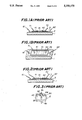
- the first type of gas sensor has, for example, a structure as shown in FIGS. 1A and 1B.
- FIG. 1A is a cross sectional view of the gas sensor
- FIG. 1B is a perspective view thereof.
- a heater layer 2 is formed on a substrate 1 having an adiabatic characteristic.
- An insulating layer 3 is formed on the heater layer 2 and electrode layers 41 and 42 are separated from each other and provided on the insulating layer 3.
- a metal-oxide semiconductor layer 51 is formed between the electrode layers 41 and 42 on the insulating layer 3 so that respective side portions of the metal-oxide layer 51 are in contact with the electrode layers 41 and 42, respectively.
- the substrate 1 is formed of a conductive material
- another insulating layer needs to be provided between the substrate 1 and the heater layer 2.
- a wire 61 is bonded on an end portion of the heater layer 2 and a wire 62 is bonded on another end portion thereof.
- Power is supplied via the wires 61 and 62 from a power supply to the heater layer 2. That is, the wires 61 and 62 function as power supplying lines.
- a wire 71 is bonded on the electrode layer 41 and a wire 72 is bonded on the electrode layer 42.
- a detecting signal is generated between wires 71 and 72.
- the wires 71 and 72 function as signal output lines.
- FIG. 2 shows another embodiment of the first type gas sensor.
- those parts which are the same as those shown in FIGS. 1A and 1B are given the same reference numbers.
- the metal-oxide semiconductor layer 51 (a gas sensitive layer) is formed on the insulating layer 3 before the electrode layers 41 and 42 are formed thereon. That is, an edge portion of each of the electrode layers 41 and 42 is provided on a corresponding edge portion of the metal-oxide semiconductor layer 51.
- the second type of gas sensor has, for example, a structure as shown in FIG. 3.
- each of the electrode pins 8 projects from both sides of the base member 12.
- a gas sensitive material which is a sinter of the metal-oxide semiconductor is mounted on the base member 12.
- the gas sensitive material 52 has, for example, a 2 or 3 mm cubic shape.
- First and second heater coils 43 and 44 are laid in the gas sensitive material 52.
- the first heater coil 43 is connected between the electrode pins 8a and 8b, and the second heater coil 44 is connected between the electrode pins 8c and 8d.
- a detecting signal is output, for example, between the electrode pin 8b connected to the first heater 43 and the electrode pin 8d connected to the second heater 44.
- the gas sensitive material 52 formed of the metal-oxide semiconductor has a relatively large size, so that power is consumed by the first and second heaters 43 and 44.
- the heat capacity of the gas sensitive material 52 is large, so that the response characteristic is poor.
- the gas sensitive material has a thin film shape, so that the power consumed by the heater layer 2 is small and the response characteristic is good.
- a sensing characteristic such as sensitivity with respect to the gas
- the sensitivity with respect to the gas deteriorates when the size of each crystal particle of the metal-oxide semiconductor increases.
- the gas sensor is generally used under a condition of 300°-450° C., so that the size of each crystal particle of the metal-oxide semiconductor increases when the gas sensor is being used for a long time.
- an absorption area in which the gas should be absorbed decreases and the chemical activation of the metal-oxide semiconductor decreases. Therefor, the sensitivity with respect to the gas decreases.
- a general object of the present invention is to provide a novel and useful gas sensor in which the disadvantages of the aforementioned prior art are eliminated.
- a more specific object of the present invention is to provide a gas sensor in which the sensing characteristic hardly deteriorates with the passage of time.
- a sensor comprising: a base member including a heater member for generating heat; a gas sensitive structure formed on the base member by a process comprising the following steps (a) and (b) of, (a) forming a stacked layer structure on the base member, the stacked layer structure including at least a metal-oxide semiconductor layer and an insulating film, and (b) carrying out a heat treatment with respect to the stacked layer structure so that a constituent of the insulating film is diffused in spaces among the crystal particles of the metal-oxide semiconductor layer; and electrode layers in contact with the gas sensitive structure.
- FIG. 1A is a cross sectional view showing a structure of a gas sensor having a thin film gas sensitive layer
- FIG. 1B is a perspective view showing a gas sensor having a thin film gas sensitive layer
- FIG. 2 is a cross sectional view showing another structure of a gas sensor having a thin film gas sensitive layer
- FIG. 3 is a perspective view showing a conventional gas sensor
- FIG. 4 is a cross sectional view showing a structure of a gas sensor having a thin film gas sensitive layer, according to a first embodiment of the present invention
- FIG. 5 shows a structure having a metal-oxide semiconductor layer and an SiO 2 layer after an annealing process
- FIG. 6 is a cross sectional view showing a structure of a gas sensor having a thin film gas sensitive layer, according to a second embodiment of the present invention.
- FIG. 7 shows a structure having a metal-oxide semiconductor layer after an annealing process for annealing
- FIG. 8 is a cross sectional view showing another structure of a gas sensor.
- a gas sensor which has a thin film metal-oxide semiconductor layer as a gas sensitive material (hereinafter referred to as a thin film type gas sensor) is normally used under a high temperature condition of 300°-450° C., so that a crystallizing process in the metal-oxide semiconductor proceeds when the thin film type gas sensor is used for a long time.
- the size of each crystal particle of the metal-oxide semiconductor increases, so that an absorption area in which the gas should be absorbed decreases, a chemical activation of the metal-oxide semiconductor decreases and so on. As a result, sensitivity with respect to the gas deteriorates.
- a high temperature (300°-450° C.) and a room temperature (for example, 25° C.) are alternately supplied to the thin film type gas sensor.
- a thermal expansion coefficient of the metal-oxide semiconductor layer differs from that of a substrate or another layer, a pull stress or a compressive stress is generated in the metal-oxide semiconductor layer.
- dislocation slips in the metal-oxide semiconductor and a hillock grows therein so that strain based on the above stress is relaxed.
- a crystal structure in the metal-oxide semiconductor layer is changed by the slipping of the dislocation and the growth of the hillock, the sensitivity with respect to the gas and the resistance thereof are changed.
- the metal-oxide semiconductor layer has been previously annealed at a high as possible temperature, the above phenomena can be prevented from being generated in the metal-oxide semiconductor.
- the strength of the metal-oxide semiconductor layer decreases and it becomes easy for the metal-oxide semiconductor layer to flake from another layer in contact therewith.
- a binder such as SiO 2 or Al 2 O 3 is added in the metal-oxide semiconductor block, it is possible to sinter the metal-oxide semiconductor at a high temperature equal to or greater than 1000° C. Also, a process for adding the binder is simple.
- a gas sensor according to the present invention has a structure made by the process comprising the steps of depositing an insulating film having a relatively high melting point on the metal-oxide semiconductor layer so that a composite structure thereof is obtained, and carrying out a heat treatment with respect to the composite structure. It has been found that it is hard for the sensing characteristic to deteriorate with the passage of time in the gas sensor having the above structure.
- a substrate 1 is made of heat resisting ceramic.
- a heater layer 2 made of platinum is formed on the substrate 1 by spattering so as to have a thin film shaped and an insulating layer 3 made of SiO 2 is formed on the heater layer 2 by spattering.
- a metal-oxide semiconductor layer 11 is formed on the insulating layer 3.
- the metal-oxide semiconductor layer 3 is made of an oxide metal such as tin (Sn), titanium (Ti), indium (In), nickel (Ni), tungsten (W), cadmium (Cd), iron (Fe), zinc (Zn) or the like.
- An insulating film 13 is formed on the metal-oxide semiconductor layer 11 by vacuum evaporation.
- the insulating film 13 is made of SiO 2 , Al 2 O 3 , Ta 2 O 5 , MgO or the like. It is desirable that the thickness of the metal-oxide semiconductor layer 11 be substantially 500 - 5000 ⁇ and the thickness of the insulating film be substantially 50 - 500 ⁇ . When the thickness of the insulating film 13 is less than 50 ⁇ , it is difficult to prevent the sensing characteristic from deteriorating with the passage of time. When the thickness of the insulating film is greater than 500 ⁇ , it is difficult to obtain enough sensitivity with respect to the gas.
- the stacked layer structure consisting of the substrate 1, the heater layer 2, the insulating layer 3, the metal-oxide semiconductor layer 11 and the insulating film 13 is annealed at a predetermined temperature for a predetermined time.
- electrode layers 41 and 42 are formed on the insulating layer 3 by spattering so that each of the electrode layers 41 and 42 is connected to a corresponding side of a structure obtained by the annealing of metal-oxide semiconductor layer 11 and the insulating film 13.
- the electrodes layer 41 and 42 can also be formed on the insulating layer 3 before the annealing process is carried out.
- the gas sensor made as described above has a sensitivity with respect to the gas which hardly deteriorates with the passage of time.
- FIG. 6 A description will now be given of another gas sensor according to the present invention with reference to FIG. 6.
- FIG. 6 those parts which are the same as those shown in FIG. 4 are given the same reference numbers.
- a plurality of metal-oxide semiconductor layers 11 and a plurality of insulating films 13 are alternately stacked on the insulating layer 3.
- the annealing process is carried out.
- the electrode layers 41 and 42 are formed on the insulating layer 3 so as to be in contact with the stacked layer structure consisting of the metal-oxide semiconductor layers 11 and the insulating layers 13. It is desirable that the thickness of each metal-oxide semiconductor layer 11 be 500-5000 ⁇ and the thickness of the insulating film 13 be 100-1000 ⁇ .
- the number of the metal-oxide semiconductor layers 11 be 2-5 and the number of the insulating films 13 be 1-4.
- the wires 61 and 62 for supplying power to the heater layer 2 are bonded on the heater layer 2, and the wires 71 and 72 for outputting the detecting signal are bonded on the electrode layers 41 and 42.
- the metal-oxide semiconductor layer 11 can be formed by vacuum evaporation, spattering or the like. It is desirable that the metal-oxide semiconductor layer 11 be formed by a "Thin Film Evaporation Apparatus" disclosed in Japanese Patent Laid Open Publication No. 59-89763. Ohta, who is one of the inventors of the present invention, is also the inventor of this apparatus.
- the present invention can also be applied to a gas detecting film in a gas sensor having a micro heater structure disclosed in Japanese Patent Laid Open Publication No.1-167645, which has been proposed by the inventors of the present invention.
- a gas sensor had a structure as shown in FIG. 4.
- a tin oxide film was formed as the metal-oxide semiconductor layer 11
- a SiO 2 film was formed as the insulating film 13.
- the tin oxide film was formed as follows.
- Metal tin (Sn) was used as the material which should be evaporated.
- a vacuum tank is previously maintained at a predetermined pressure in the order of 10 -4 Pa, and then oxygen gas was brought into the vacuum tank so that the pressure in the vacuum tank was controlled at 0.2 Pa.
- a current of 70A was supplied to a filament so that electrons were generated from the filament, and then a voltage of about 100 V was supplied to a grid so that plasma was generated.
- the tin oxide film grew at a speed of about 20 ⁇ /sec., so that a tin oxide film of 3000 ⁇ is formed.
- SiO 2 was formed on the Tin oxide film as follows.
- Oxygen gas was brought into the vacuum tank so that the pressure in the vacuum tank was controlled at 0.1 Pa. Under this condition, SiO was evaporated by a resistor heating process so that a SiO 2 film of 100 ⁇ was formed on the tin oxide film.
- the thin film type gas sensor having the stacked layer structure was annealed for 3 hours in oxygen gas at 1000° C.
- the tin oxide film formed in accordance with the above process was firm so it did not flake from a layer on which the tin oxide film was formed.
- the sensitivity with respect to the gas was high enough.
- the gas sensor having the above structure is used at 450° C. for 300 days, the sensitivity with respect to the gas does not deteriorate at all.
- Tin oxide is finely crystallized by the annealing process, and then, as shown in FIG. 5, SiO 2 22 is diffused in spaces among crystal particles 21 of tin oxide.
- the SiO 2 22 diffused in the spaces among the crystal particles 21 functions as a binder so that the tin oxide film becomes firm and the size of each of the crystal particles 21 is prevented from increasing.
- a gas sensor had a structure as shown in FIG. 6.
- a tin oxide film was formed as the metal-oxide semiconductor layer 11
- a SiO 2 film was formed as the insulating film 13.
- the tin oxide film is formed as follows.
- Metal tin (Sn) was used as a material which should be evaporated.
- a vacuum tank was previously maintained at a predetermined pressure in the order of 10 -4 Pa, and then oxygen gas was brought into the vacuum tank so that the pressure in the vacuum tank was controlled at 0.2 Pa.
- a current of 70 ⁇ was supplied to a filament so that electrons were generated from the filament, and then a voltage of about 100 V was supplied to a grid so that plasma was generated.
- the tin oxide film grew at a speed of about 20 ⁇ /sec., so that the tin oxide film of 3000 ⁇ was formed.
- SiO 2 was formed on the Tin oxide film as follows.
- Oxygen gas was brought into the vacuum tank so that the pressure in the vacuum tank was controlled at 0.1 Pa. Under this condition, SiO was evaporated by a resistor heating process so that a SiO 2 film of 100A was formed on the tin oxide film.
- the tin oxide films and the SiO 2 films, which are formed in accordance with the above processes, are alternately stacked. There are three tin oxide films and each tin oxide film has a 1000 ⁇ thickness. There are two SiO 2 is two and each SiO 2 film has a 100 ⁇ thickness.
- the thin film type gas sensor having the stacked layer structure is annealed for 3 hours in oxygen gas at 1000° C.
- each tin oxide film formed in accordance with the above process is firm so as not to flake from a layer on which each tin oxide film is formed.
- the sensitivity with respect to the gas is also sufficiently high.
- the gas sensor having the above structure is used at 450° C. for 300 days, the sensitivity with respect to the gas does not deteriorate at all.
- Tin oxide is finely crystallized by the annealing process, and then, as shown in FIG. 7, SiO 2 22 is diffused in spaces among the crystal particles 21 of tin oxide.
- the SiO 2 22 diffused in the spaces among the crystal particles 21 functions as a binder so that the tin oxide film becomes firm and the size of each crystal particle 21 is prevented from increasing.
- the heater layer 2 can be provided on a surface of the substrate 1, opposite to the surface on which the metal-oxide semiconductor layer 51 is provided, as shown in FIG. 8.
Abstract
Description
Claims (12)
SiO.sub.2, Al.sub.2 O.sub.3, Ta.sub.2 O.sub.5, and Mgo.
SiO.sub.2, Al.sub.2 O.sub.3, Ta.sub.2 OI.sub.5, and MgO.
Applications Claiming Priority (6)
| Application Number | Priority Date | Filing Date | Title |
|---|---|---|---|
| JP2-65258 | 1990-03-15 | ||
| JP6525890 | 1990-03-15 | ||
| JP15040890 | 1990-06-08 | ||
| JP2-150408 | 1990-06-08 | ||
| JP23969190A JPH04127047A (en) | 1990-03-15 | 1990-09-10 | Gas sensor |
| JP2-239691 | 1990-09-10 |
Publications (1)
| Publication Number | Publication Date |
|---|---|
| US5250170A true US5250170A (en) | 1993-10-05 |
Family
ID=27298726
Family Applications (1)
| Application Number | Title | Priority Date | Filing Date |
|---|---|---|---|
| US07/668,617 Expired - Lifetime US5250170A (en) | 1990-03-15 | 1991-03-13 | Gas sensor having metal-oxide semiconductor layer |
Country Status (1)
| Country | Link |
|---|---|
| US (1) | US5250170A (en) |
Cited By (31)
| Publication number | Priority date | Publication date | Assignee | Title |
|---|---|---|---|---|
| US5372785A (en) * | 1993-09-01 | 1994-12-13 | International Business Machines Corporation | Solid-state multi-stage gas detector |
| US5536473A (en) * | 1993-01-13 | 1996-07-16 | British Gas Plc | Polyaniline gas sensor |
| US5599584A (en) * | 1994-12-16 | 1997-02-04 | Mine Safety Appliances Company | Microminiature combustible gas sensor and method of fabricating a microminiature combustible gas sensor |
| EP0768528A2 (en) * | 1995-10-16 | 1997-04-16 | General Motors Corporation | Hydrogen sensor |
| US5698771A (en) * | 1995-03-30 | 1997-12-16 | The United States Of America As Represented By The United States National Aeronautics And Space Administration | Varying potential silicon carbide gas sensor |
| US5747669A (en) * | 1995-12-28 | 1998-05-05 | Fujitsu Limited | Oxygen electrode and its manufacture |
| US5786608A (en) * | 1996-03-14 | 1998-07-28 | Motorola, Inc. | Semiconductor chemical sensor device with specific heater structure |
| US5830412A (en) * | 1993-09-30 | 1998-11-03 | Nittan Company Limited | Sensor device, and disaster prevention system and electronic equipment each having sensor device incorporated therein |
| WO1998049547A1 (en) * | 1997-04-30 | 1998-11-05 | T/J Technologies, Inc. | Chemical sensors and methods for their use |
| EP0878707A1 (en) * | 1996-10-22 | 1998-11-18 | Kabushiki Kaisha Riken | Heating-type sensor |
| US5948361A (en) * | 1996-08-27 | 1999-09-07 | Motorola, Inc. | Chemical sensor and method of making same |
| US6041643A (en) * | 1998-07-27 | 2000-03-28 | General Electric Company | Gas sensor with protective gate, method of forming the sensor, and method of sensing |
| ES2142273A1 (en) * | 1998-03-13 | 2000-04-01 | Gas De Euskadi S A Soc De | Gas sensor |
| US6059937A (en) * | 1995-12-22 | 2000-05-09 | Korea Gas Corporation | Sensor having tin oxide thin film for detecting methane gas and propane gas, and process for manufacturing thereof |
| US6109094A (en) * | 1994-09-23 | 2000-08-29 | Forskarpatent I Linkoping Ab | Method and device for gas sensing |
| US6155160A (en) * | 1998-06-04 | 2000-12-05 | Hochbrueckner; Kenneth | Propane detector system |
| US6463789B2 (en) * | 2000-03-09 | 2002-10-15 | Dornier Gmbh | Gas sensor |
| US20060000259A1 (en) * | 2004-05-17 | 2006-01-05 | Massachusetts Institute Of Technology | Photo-induced sensitivity and selectivity of semiconductor gas sensors |
| US20060185420A1 (en) * | 2005-02-22 | 2006-08-24 | Ngk Spark Plug Co., Ltd. | Gas sensor |
| US20060249384A1 (en) * | 2004-12-22 | 2006-11-09 | Kim Yong S | Chemical sensor |
| US20060270053A1 (en) * | 2005-05-26 | 2006-11-30 | General Electric Company | Apparatus, methods, and systems having gas sensor with catalytic gate and variable bias |
| US20100263437A1 (en) * | 2009-04-15 | 2010-10-21 | Nihon Dempa Kogyo Co., Ltd | Quartz sensor and sensing device |
| US20170016866A1 (en) * | 2015-07-13 | 2017-01-19 | International Business Machines Corporation | Reconfigurable gas sensor architecture with a high sensitivity at low temperatures |
| WO2017205146A1 (en) * | 2016-05-27 | 2017-11-30 | Carrier Corporation | Gas detection device and method of manufacturing the same |
| US10132769B2 (en) | 2016-07-13 | 2018-11-20 | Vaon, Llc | Doped, metal oxide-based chemical sensors |
| US20190285564A1 (en) * | 2016-10-05 | 2019-09-19 | Hewlett-Packard Development Company, L.P. | Insulated sensors |
| US10802008B2 (en) | 2017-02-28 | 2020-10-13 | Vaon, Llc | Bimetal doped-metal oxide-based chemical sensors |
| US11203183B2 (en) | 2016-09-27 | 2021-12-21 | Vaon, Llc | Single and multi-layer, flat glass-sensor structures |
| US11275051B2 (en) | 2016-03-23 | 2022-03-15 | Vaon, Llc | Metal oxide-based chemical sensors |
| US11467138B2 (en) | 2016-09-27 | 2022-10-11 | Vaon, Llc | Breathalyzer |
| US11686697B2 (en) | 2020-09-24 | 2023-06-27 | International Business Machines Corporation | Multifunctional heterojunction metal oxide gas sensor |
Citations (2)
| Publication number | Priority date | Publication date | Assignee | Title |
|---|---|---|---|---|
| US4580439A (en) * | 1983-02-07 | 1986-04-08 | Ricoh Seiki Co., Ltd. | Low power gas detector |
| US5003812A (en) * | 1987-12-23 | 1991-04-02 | Ricoh Company, Ltd. | Gas detecting device |
-
1991
- 1991-03-13 US US07/668,617 patent/US5250170A/en not_active Expired - Lifetime
Patent Citations (2)
| Publication number | Priority date | Publication date | Assignee | Title |
|---|---|---|---|---|
| US4580439A (en) * | 1983-02-07 | 1986-04-08 | Ricoh Seiki Co., Ltd. | Low power gas detector |
| US5003812A (en) * | 1987-12-23 | 1991-04-02 | Ricoh Company, Ltd. | Gas detecting device |
Cited By (45)
| Publication number | Priority date | Publication date | Assignee | Title |
|---|---|---|---|---|
| US5536473A (en) * | 1993-01-13 | 1996-07-16 | British Gas Plc | Polyaniline gas sensor |
| US5372785A (en) * | 1993-09-01 | 1994-12-13 | International Business Machines Corporation | Solid-state multi-stage gas detector |
| US5830412A (en) * | 1993-09-30 | 1998-11-03 | Nittan Company Limited | Sensor device, and disaster prevention system and electronic equipment each having sensor device incorporated therein |
| US6109094A (en) * | 1994-09-23 | 2000-08-29 | Forskarpatent I Linkoping Ab | Method and device for gas sensing |
| US5599584A (en) * | 1994-12-16 | 1997-02-04 | Mine Safety Appliances Company | Microminiature combustible gas sensor and method of fabricating a microminiature combustible gas sensor |
| US5698771A (en) * | 1995-03-30 | 1997-12-16 | The United States Of America As Represented By The United States National Aeronautics And Space Administration | Varying potential silicon carbide gas sensor |
| EP0768528A2 (en) * | 1995-10-16 | 1997-04-16 | General Motors Corporation | Hydrogen sensor |
| EP0768528A3 (en) * | 1995-10-16 | 1997-04-23 | General Motors Corporation | Hydrogen sensor |
| US6059937A (en) * | 1995-12-22 | 2000-05-09 | Korea Gas Corporation | Sensor having tin oxide thin film for detecting methane gas and propane gas, and process for manufacturing thereof |
| US5747669A (en) * | 1995-12-28 | 1998-05-05 | Fujitsu Limited | Oxygen electrode and its manufacture |
| US6083367A (en) * | 1995-12-28 | 2000-07-04 | Fujitsu Limited | Oxygen electrode and its manufacture |
| US5786608A (en) * | 1996-03-14 | 1998-07-28 | Motorola, Inc. | Semiconductor chemical sensor device with specific heater structure |
| US5948361A (en) * | 1996-08-27 | 1999-09-07 | Motorola, Inc. | Chemical sensor and method of making same |
| EP0878707A1 (en) * | 1996-10-22 | 1998-11-18 | Kabushiki Kaisha Riken | Heating-type sensor |
| EP0878707A4 (en) * | 1996-10-22 | 2000-06-28 | Riken Kk | Heating-type sensor |
| WO1998049547A1 (en) * | 1997-04-30 | 1998-11-05 | T/J Technologies, Inc. | Chemical sensors and methods for their use |
| ES2142273A1 (en) * | 1998-03-13 | 2000-04-01 | Gas De Euskadi S A Soc De | Gas sensor |
| US6155160A (en) * | 1998-06-04 | 2000-12-05 | Hochbrueckner; Kenneth | Propane detector system |
| US6041643A (en) * | 1998-07-27 | 2000-03-28 | General Electric Company | Gas sensor with protective gate, method of forming the sensor, and method of sensing |
| US6463789B2 (en) * | 2000-03-09 | 2002-10-15 | Dornier Gmbh | Gas sensor |
| US20060000259A1 (en) * | 2004-05-17 | 2006-01-05 | Massachusetts Institute Of Technology | Photo-induced sensitivity and selectivity of semiconductor gas sensors |
| US20080110241A1 (en) * | 2004-05-17 | 2008-05-15 | Avner Rothschild | Photo-induced sensitivity and selectivity of semiconductor gas sensors |
| US20060249384A1 (en) * | 2004-12-22 | 2006-11-09 | Kim Yong S | Chemical sensor |
| US7276745B2 (en) | 2005-02-22 | 2007-10-02 | Ngk Spark Plug Co., Ltd. | Gas sensor |
| US20060185420A1 (en) * | 2005-02-22 | 2006-08-24 | Ngk Spark Plug Co., Ltd. | Gas sensor |
| US20060270053A1 (en) * | 2005-05-26 | 2006-11-30 | General Electric Company | Apparatus, methods, and systems having gas sensor with catalytic gate and variable bias |
| US20100263437A1 (en) * | 2009-04-15 | 2010-10-21 | Nihon Dempa Kogyo Co., Ltd | Quartz sensor and sensing device |
| US8464577B2 (en) * | 2009-04-15 | 2013-06-18 | Nihon Dempa Kogyo Co., Ltd. | Quartz sensor and sensing device |
| US10697928B2 (en) * | 2015-07-13 | 2020-06-30 | International Business Machines Corporation | Reconfigurable gas sensor architecture with a high sensitivity at low temperatures |
| US20170024992A1 (en) * | 2015-07-13 | 2017-01-26 | International Business Machines Corporation | Reconfigurable gas sensor architecture with a high sensitivity at low temperatures |
| US20170023520A1 (en) * | 2015-07-13 | 2017-01-26 | International Business Machines Corporation | Reconfigurable gas sensor architecture with a high sensitivity at low temperatures |
| US20170016866A1 (en) * | 2015-07-13 | 2017-01-19 | International Business Machines Corporation | Reconfigurable gas sensor architecture with a high sensitivity at low temperatures |
| US10670554B2 (en) * | 2015-07-13 | 2020-06-02 | International Business Machines Corporation | Reconfigurable gas sensor architecture with a high sensitivity at low temperatures |
| US10697927B2 (en) * | 2015-07-13 | 2020-06-30 | International Business Machines Corporation | Reconfigurable gas sensor architecture with a high sensitivity at low temperatures |
| US11275051B2 (en) | 2016-03-23 | 2022-03-15 | Vaon, Llc | Metal oxide-based chemical sensors |
| WO2017205146A1 (en) * | 2016-05-27 | 2017-11-30 | Carrier Corporation | Gas detection device and method of manufacturing the same |
| US11513091B2 (en) | 2016-05-27 | 2022-11-29 | Carrier Corporation | Gas detection device and method of manufacturing the same |
| US10132769B2 (en) | 2016-07-13 | 2018-11-20 | Vaon, Llc | Doped, metal oxide-based chemical sensors |
| US11009475B2 (en) | 2016-07-13 | 2021-05-18 | Vaon, Llc | Doped, metal oxide-based chemical sensors |
| US11467138B2 (en) | 2016-09-27 | 2022-10-11 | Vaon, Llc | Breathalyzer |
| US11203183B2 (en) | 2016-09-27 | 2021-12-21 | Vaon, Llc | Single and multi-layer, flat glass-sensor structures |
| US20190285564A1 (en) * | 2016-10-05 | 2019-09-19 | Hewlett-Packard Development Company, L.P. | Insulated sensors |
| US10876986B2 (en) * | 2016-10-05 | 2020-12-29 | Hewlett-Packard Development Company, L.P. | Insulated sensors |
| US10802008B2 (en) | 2017-02-28 | 2020-10-13 | Vaon, Llc | Bimetal doped-metal oxide-based chemical sensors |
| US11686697B2 (en) | 2020-09-24 | 2023-06-27 | International Business Machines Corporation | Multifunctional heterojunction metal oxide gas sensor |
Similar Documents
| Publication | Publication Date | Title |
|---|---|---|
| US5250170A (en) | Gas sensor having metal-oxide semiconductor layer | |
| US4350743A (en) | Structure for multilayer circuits | |
| US4766411A (en) | Use of compositionally modulated multilayer thin films as resistive material | |
| US5147523A (en) | Thin film gas sensor | |
| JPH0936309A (en) | Manufacture of capacitor element | |
| JP5336684B2 (en) | Platinum bottom electrode and ferroelectric capacitor manufacturing method | |
| US4276535A (en) | Thermistor | |
| US5258884A (en) | Magnetoresistive read transducer containing a titanium and tungsten alloy spacer layer | |
| JP2001313376A6 (en) | Method of manufacturing platinum lower electrode and ferroelectric capacitor, and ferroelectric capacitor | |
| JP3217632B2 (en) | Products containing improved magnetoresistive materials | |
| US3188594A (en) | Thermally sensitive resistances | |
| US20030174041A1 (en) | Temperature sensor | |
| US3898359A (en) | Thin film magneto-resistors and methods of making same | |
| Neuman et al. | Structural dependence of strain gauge effect and surface resistivity for thin gold films | |
| Kampwirth et al. | Application of high rate magnetron sputtering to the fabrication of A-15 compounds | |
| US4338145A (en) | Chrome-tantalum alloy thin film resistor and method of producing the same | |
| WO1986004989A1 (en) | Gas sensor element of tin oxide film | |
| US4358783A (en) | Superconducting thin films | |
| JPS62128015A (en) | Magneto-resistance effect type magnetic head | |
| Krongelb et al. | Annealing of thin magnetoresistive permalloy films | |
| US5316973A (en) | Method of making semiconducting ferroelectric PTCR devices | |
| Khan et al. | Structure and oxidation of thin gold‐nickel alloy films | |
| Naoe et al. | Properties of (Fe, Co)-(Ta, W) amorphous alloy films deposited by rf sputtering | |
| JPS6258554B2 (en) | ||
| JPH04127047A (en) | Gas sensor |
Legal Events
| Date | Code | Title | Description |
|---|---|---|---|
| AS | Assignment |
Owner name: RICOH COMPANY, LTD., JAPAN Free format text: ASSIGNMENT OF ASSIGNORS INTEREST;ASSIGNORS:YAGAWARA, SHINJI;OHTA, WASABURO;REEL/FRAME:006578/0239 Effective date: 19910308 |
|
| STCF | Information on status: patent grant |
Free format text: PATENTED CASE |
|
| FEPP | Fee payment procedure |
Free format text: PAYOR NUMBER ASSIGNED (ORIGINAL EVENT CODE: ASPN); ENTITY STATUS OF PATENT OWNER: LARGE ENTITY |
|
| FPAY | Fee payment |
Year of fee payment: 4 |
|
| FPAY | Fee payment |
Year of fee payment: 8 |
|
| FEPP | Fee payment procedure |
Free format text: PAYER NUMBER DE-ASSIGNED (ORIGINAL EVENT CODE: RMPN); ENTITY STATUS OF PATENT OWNER: LARGE ENTITY Free format text: PAYOR NUMBER ASSIGNED (ORIGINAL EVENT CODE: ASPN); ENTITY STATUS OF PATENT OWNER: LARGE ENTITY |
|
| FPAY | Fee payment |
Year of fee payment: 12 |