US5225945A - Apparatus for editing pcm signals reproduced at different speeds from two memories - Google Patents
Apparatus for editing pcm signals reproduced at different speeds from two memories Download PDFInfo
- Publication number
- US5225945A US5225945A US07/313,174 US31317489A US5225945A US 5225945 A US5225945 A US 5225945A US 31317489 A US31317489 A US 31317489A US 5225945 A US5225945 A US 5225945A
- Authority
- US
- United States
- Prior art keywords
- edit
- editing
- pcm
- point
- pcm audio
- Prior art date
- Legal status (The legal status is an assumption and is not a legal conclusion. Google has not performed a legal analysis and makes no representation as to the accuracy of the status listed.)
- Expired - Lifetime
Links
- 230000015654 memory Effects 0.000 title claims abstract description 70
- 238000005562 fading Methods 0.000 claims abstract description 11
- 230000005236 sound signal Effects 0.000 abstract description 55
- 230000006870 function Effects 0.000 abstract description 2
- 238000010586 diagram Methods 0.000 description 6
- 238000000034 method Methods 0.000 description 5
- 238000005070 sampling Methods 0.000 description 5
- 239000003550 marker Substances 0.000 description 4
- 230000008859 change Effects 0.000 description 2
- 238000012544 monitoring process Methods 0.000 description 2
- 230000004044 response Effects 0.000 description 2
- 101100171405 Danio rerio dvr1 gene Proteins 0.000 description 1
- 230000007246 mechanism Effects 0.000 description 1
- 238000012986 modification Methods 0.000 description 1
- 230000004048 modification Effects 0.000 description 1
- 230000000007 visual effect Effects 0.000 description 1
Images


Classifications
-
- G—PHYSICS
- G11—INFORMATION STORAGE
- G11B—INFORMATION STORAGE BASED ON RELATIVE MOVEMENT BETWEEN RECORD CARRIER AND TRANSDUCER
- G11B27/00—Editing; Indexing; Addressing; Timing or synchronising; Monitoring; Measuring tape travel
- G11B27/02—Editing, e.g. varying the order of information signals recorded on, or reproduced from, record carriers
- G11B27/031—Electronic editing of digitised analogue information signals, e.g. audio or video signals
- G11B27/036—Insert-editing
-
- G—PHYSICS
- G11—INFORMATION STORAGE
- G11B—INFORMATION STORAGE BASED ON RELATIVE MOVEMENT BETWEEN RECORD CARRIER AND TRANSDUCER
- G11B27/00—Editing; Indexing; Addressing; Timing or synchronising; Monitoring; Measuring tape travel
- G11B27/002—Programmed access in sequence to a plurality of record carriers or indexed parts, e.g. tracks, thereof, e.g. for editing
-
- G—PHYSICS
- G11—INFORMATION STORAGE
- G11B—INFORMATION STORAGE BASED ON RELATIVE MOVEMENT BETWEEN RECORD CARRIER AND TRANSDUCER
- G11B27/00—Editing; Indexing; Addressing; Timing or synchronising; Monitoring; Measuring tape travel
- G11B27/02—Editing, e.g. varying the order of information signals recorded on, or reproduced from, record carriers
- G11B27/031—Electronic editing of digitised analogue information signals, e.g. audio or video signals
- G11B27/038—Cross-faders therefor
-
- G—PHYSICS
- G11—INFORMATION STORAGE
- G11B—INFORMATION STORAGE BASED ON RELATIVE MOVEMENT BETWEEN RECORD CARRIER AND TRANSDUCER
- G11B27/00—Editing; Indexing; Addressing; Timing or synchronising; Monitoring; Measuring tape travel
- G11B27/10—Indexing; Addressing; Timing or synchronising; Measuring tape travel
- G11B27/34—Indicating arrangements
-
- G—PHYSICS
- G11—INFORMATION STORAGE
- G11B—INFORMATION STORAGE BASED ON RELATIVE MOVEMENT BETWEEN RECORD CARRIER AND TRANSDUCER
- G11B2220/00—Record carriers by type
- G11B2220/90—Tape-like record carriers
-
- G—PHYSICS
- G11—INFORMATION STORAGE
- G11B—INFORMATION STORAGE BASED ON RELATIVE MOVEMENT BETWEEN RECORD CARRIER AND TRANSDUCER
- G11B2220/00—Record carriers by type
- G11B2220/90—Tape-like record carriers
- G11B2220/91—Helical scan format, wherein tracks are slightly tilted with respect to tape direction, e.g. VHS, DAT, DVC, AIT or exabyte
- G11B2220/913—Digital audio tape [DAT] format
-
- G—PHYSICS
- G11—INFORMATION STORAGE
- G11B—INFORMATION STORAGE BASED ON RELATIVE MOVEMENT BETWEEN RECORD CARRIER AND TRANSDUCER
- G11B27/00—Editing; Indexing; Addressing; Timing or synchronising; Monitoring; Measuring tape travel
- G11B27/02—Editing, e.g. varying the order of information signals recorded on, or reproduced from, record carriers
- G11B27/031—Electronic editing of digitised analogue information signals, e.g. audio or video signals
- G11B27/032—Electronic editing of digitised analogue information signals, e.g. audio or video signals on tapes
-
- G—PHYSICS
- G11—INFORMATION STORAGE
- G11B—INFORMATION STORAGE BASED ON RELATIVE MOVEMENT BETWEEN RECORD CARRIER AND TRANSDUCER
- G11B27/00—Editing; Indexing; Addressing; Timing or synchronising; Monitoring; Measuring tape travel
- G11B27/36—Monitoring, i.e. supervising the progress of recording or reproducing
Definitions
- the present invention relates to an apparatus for editing PCM signals and, more particularly, to an apparatus having an electronic editing function to edit PCM signals with means of storing the edit-point proximate signals in memories.
- an editing start point and an editing end point are determined individually in an insert editing mode by a memory rehearsal which confirms the editing state by reading out the stored sample data from the memories and monitoring the analog reproduced sound, and thereafter both the apparatus for reproducing the new PCM audio signal and the apparatus for reproducing the previously recorded PCM audio signal are driven synchronously with each other in a playback mode to actually run the tapes, and a preview is executed to monitor the reproduced sound for a relatively long time. Therefore the editing efficiency is rendered extremely low and the tapes need to be repeatedly driven to eventually bring about a problem of additional burdens on the mechanisms.
- modifications with insert editing are frequently adopted posterior to an assemble editing mode, and in the actual insert editing, there are many cases of replacing musical notes or the like of several or less seconds, so that it becomes necessary to enhance the short-time insert editing efficiency.
- the procedure of setting the edit point can be executed accurately by a memory rehearsal with relative simplicity, but in editing the signals with regard to fast-touch piano music or the like, it is still extremely difficult to achieve exact determination of the edit point even with such memory rehearsal. And there exists another problem that a proper grasp is impossible with regard to the cross-fade conditions of PCM audio signals at the edit point.
- display means is provided for displaying the operational states of the reproducing-side tape recorder and the recording-side tape recorder by the use of symbols and messages as well as for numerically displaying the present tape running position in each tape recorder, the editing start point and the editing end point with respect to the time code recorded on the tape.
- the editor is enabled to advance the editing procedure while confirming the operational state of each tape recorder, the present tape position and so forth therein.
- a principal object of the present invention resides in providing a PCM signal editing apparatus which ensures high efficiency and sufficient certainty in performing an editing operation.
- Another object of the invention is to provide a PCM signal editing apparatus adapted to execute short-time insert editing of several or less seconds efficiently and certainly.
- a further object of the invention resides in providing a PCM signal editing apparatus so contrived as to perform an efficient and certain editing operation with regard to, for example, fast-touch piano music or the like.
- a more specific object of the invention is to provide a PCM signal editing apparatus which is capable of reading out the sample data of edit-point proximate PCM signals from memories at a desired speed, then cross-fading the sample data in a time conforming with such read-out speed, and executing a memory rehearsal at a selected speed.
- a further object of the invention is to provide a PCM signal editing apparatus which enables the editor to know accurately and simply that the sound being monitored corresponds to which of the data stored in the memories.
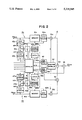
- a PCM signal editing apparatus comprising first input circuit means for receiving a first PCM signal from a reproducing apparatus; second input circuit means for receiving a second PCM signal from a reproducing and recording apparatus; first memory means for storing the first PCM signal; second memory means for storing the second PCM signal; editing circuit means for connecting the first and second PCM signals mutually and outputting an edited PCM signal; and edit control means for reading out the first and second PCM signals from the first and second memory means respectively and controlling the editing circuit means.
- FIG. 1 is a block diagram of an exemplary embodiment of the PCM signal editing apparatus according to the present invention.
- FIG. 2 is a block diagram of an editing processor employed in the editing apparatus shown in FIG. 1;
- FIG. 3A schematically illustrates the contents of control coefficient data fed in a normal read mode from a cross-fade controller shown in FIG. 2;
- FIG. 3B schematically illustrates the contents of control coefficient data fed in a slow read mode from the cross-fade controller shown in FIG. 2;
- FIGS. 4A and 4B are schematic diagrams respectively showing how PCM audio signals obtained in a normal read mode and a slow read mode are connected to each other in an assemble editing mode and a rehearsal thereof;
- FIG. 4C is a schematic diagram showing how PCM audio signals are connected to each other in an insert editing mode and a rehearsal thereof;
- FIG. 5A schematically illustrates the display areas on a display unit in the editing apparatus of FIG. 1;
- FIGS. 5B and 5C schematically illustrate exemplary display contents of the display unit of FIG. 5A in the assemble editing mode and the insert editing mode.
- a PCM signal editing apparatus 3 is connected to both a helical scanning type digital video tape recorder (DVTR) 1 used as a recording apparatus and a fixed head type digital audio tape recorder (DAT) 2 used as a reproducing apparatus.
- DVTR digital video tape recorder
- DAT fixed head type digital audio tape recorder
- Each of such DVTR 1 and DAT 2 includes, although not shown, an encoder and a decoder therein, and PCM audio signals at the input and output terminals of the DVTR 1 and DAT 2 are shaped to have the same format.
- the editing apparatus 3 is fed with both a reproduced PCM audio signal PB DVR obtained at the playback output terminal of the DVTR 1 and a reproduced PCM audio Signal PB DAT obtained at the playback output terminal of the DAT 2.
- the editing apparatus 3 is equipped with an editing processor 4, and an edited PCM audio signal ED DVTR outputted from the editing processor 4 is supplied to the recording input terminal of the DVTR 1.
- the editing apparatus 3 has a selector switch 5 for selectively outputting either the reproduced PCM audio signal PB DVTR obtained from DVTR 1, the reproduced PCM audio signal PB DAT obtained from the DAT 2 or the edited PCM audio signal ED DVTR from the editing processor 4, and an audio signal produced by converting each of the PCM audio signals PB DVTR , PB DAT and ED DVTR into an analog form through a digital-to-analog (D/A) converter 6 is supplied via an audio amplifier 7 to a monitor speaker 8.
- D/A digital-to-analog
- the edited PCM audio signal ED DVTR outputted from the editing processor 4 is supplied to the switch 5 via a delay circuit 9 which has a delay time equal to the sum of the respective data processing times of the decoder 3 in the DAT 2 and the encoder 5 in the DVTR 1.
- the editing apparatus 3 is further equipped with manual input means such as a fader 10, a keyboard 11 and a jog dial 12; a controller 13 to receive input data therefrom; and a display unit 14 driven under control of such controller 13.
- the controller 13 executes remote control of the DVTR 1 and the DAT 2, operation control of the editing processor 4 and the selector switch 5, and display control of the display unit 14.
- the editing processor 4 is so constituted as shown in the block diagram of FIG. 2, wherein the reproduced PCM audio Signal PB DVTR obtained from the playback output terminal of the DVTR 1 is supplied to both a first memory 41a and a clock extracting circuit 42a in a recording-side processing circuit 4a.
- the clock extracting circuit 42a is a circuit for extracting word clock pulses wck a1 from the reproduced PCM audio signal; PB DVR , and such word clock pulses wck a1 are supplied from a changeover switch 43a via a programmable frequency divider 44a to an address counter 45a.
- the address counter 45a serves to count the clock pulses supplied from the frequency divider 44a and thereby forms address data ADR a for the first memory 41a.
- the address data ADR a is supplied to the first memory 41a while being supplied also to a latch circuit 46a.
- the recording-side processing circuit 4a includes a clock generator 47a driven under control of the controller 13, and the word clock pulses wck a2 obtained from the clock generator 47a are supplied from the changeover switch 43a via the programmable frequency divider 44a to the address counter 45a.
- All of the changeover switch 43a, the programmable frequency divider 44a and the address counter 45a are driven under control of the controller 13.
- the clock extracting circuit 42a is connected by the changeover switch 43a to the programmable frequency divider 44a whose division ratio is set to 1, and the sample data of the reproduced PCM audio signal PB DVTR is sequentially written in the first memory 41a in accordance with the address data ADR a formed by the address counter 45a on the basis of the word clock pulses wck a1 extracted by the clock sampler 42a.
- the controller 13 In response to the input data indicative of the edit point P 1 and received from the keyboard 11 in the write mode, the controller 13 loads the address data ADR 1 at such timing through the latch circuit 46a. And the data writing operation with regard to the first memory 41a is completed at the instant the address data ADR a formed by the address counter 45a has advanced from the address data ADR 1 by an amount equivalent to half the storage capacity of the first memory 41a.
- the reproduced PCM audio signal PB DAT obtained from the playback output terminal of the DAT 2 is supplied to both a second memory 41b and a clock extracting circuit 42b.
- the clock extracting circuit 42b is a circuit to produce word clock pulses wck b1 from the reproduced PCM audio signal PB DAT , and such word clock pulses wck b1 are supplied from a changeover switch 43b via a programmable frequency divider 44b to an address counter 45b.
- the address counter 45b serves to count the clock pulses supplied from the programmable frequency divider 44b and thereby forms address data ADR b for the second memory 41b.
- the address data ADR b is supplied to the second memory 41b while being supplied also to a latch circuit 46b.
- the reproducing-side processing circuit 4b includes a clock generator 49b driven under control of the controller 13, and the clock pulses obtained from the clock generator 49b are supplied from the changeover switch 43b via the programmable frequency divider 44b to the address counter 45b.
- All of the changeover switch 43b, the programmable frequency divider 44b and the address counter 45b are driven under control of the controller 13.
- the clock extracting circuit 42b is connected by the selector switch 43b to the programmable frequency divider 44b whose division ratio is set to 1, and the sample data of the reproduced PCM audio signal PB DAT is sequentially written in the second memory 41b in accordance with the address data ADR b formed by the address counter 45b on the basis of the word clock pulses wck b1 extracted by the clock extracting circuit 42b.
- the controller 13 In response to the input data indicative of the edit point P 2 and received from the keyboard 11 in the write mode, the controller 13 loads the address data ADR 2 at such timing through the latch circuit 46b. And the data writing operation with regard to the second memory 41b is completed at the moment the address data ADR b formed by the address counter 45b has advanced from the address data ADR 2 by an amount equivalent to half the storage capacity of the second memory 41b.
- the controller 13 loads merely the address data ADR IN1 and ADR IN2 indicative of the editing start points or edit-in points P IN1 and P IN2 of the sample data in the memories 41a and 41b. Meanwhile, in an insert editing mode where two edit points are existent, the controller 13 first loads, in the aforementioned recording mode, the address data ADR IN1 and ADR IN2 indicative of the edit-in points P IN1 and P IN2 within the range of the storage capacities of the memories 41a and 41b.
- the controller 13 determines the editing end point or edit-out point P OUT1 by the undermentioned method, then loads the address data ADR OUT1 indicative of such edit-out point, and automatically calculates the address data ADR OUT2 , which indicates the edit-out point P OUT2 of the sample data in the second memory 41b, in accordance with the address difference between the edit-in point P IN1 and the edit-out point P OUT1 of the sample data written in the first memory 41a.
- controller 13 feeds to the data comparators 48 and 49 the address data ADR IN1 indicative of the edit-in point P IN1 in the assemble editing mode, or the address data ADR IN1 indicative of the edit-in point P IN1 and the address data ADR OUT1 indicative of the edit-out point P OUT1 in the insert editing mode.
- the address data ADR a formed by the address counter 45a is compared with the address data ADR IN1 and ADR OUT1 indicative of the edit point fed from the controller 13, whereby edit-point timing signals are formed.
- word clock pulses wck a2 or wck b2 of a predetermined frequency are outputted from the clock generator 47a or 47b, and the sample data of the reproduced PCM audio signal PB DVTR or PB DAT proximate to the edit points P 1 and P 2 are read out from the first memory 41a or the second memory 41b in accordance with the address data ADR a or ADR b formed by the address counter 45a or 45b on the basis of the word clock pulses wck a2 or wck b2 .
- the sample data thus read out from the first memory 41a is supplied via an interpolator 50a to a cross-fading multiplier 51a, which then multiplies the input signal by control coefficient data ⁇ fed from the cross-fade controller 52 at the timing t 0 of the edit point P 1 obtained from the comparator 48, whereby the sample data is faded and then is supplied to the data adder 54.
- the sample data read out from the second memory 41b is supplied via an interpolator 50b to a cross-fading multiplier 51b, which then multiplies the input signal by control coefficient data ⁇ -1 fed from the cross-fade controller 52 at the timing t 0 of the edit point P 2 obtained from the comparator 48, whereby the sample data is faded and then is supplied to the data adder 54 via the level adjusting multiplier 53.
- the added output data obtained from the data adder 54 is fed to a multiplier 55, which fades the initial and terminal portions of the edited output and produces an edited PCM audio signal ED DVTR .
- the controller 13 presets the address counters 45a and 45b in a manner to attain a timing coincidence with regard to the edit points so that, in a rehearsal mode or an edited output mode, the data of the reproduced PCM signals PB DVTR and PB DAT can be read out successively at the edit points from the memories 41a and 41b where the reproduced PCM audio signals PB DVTR and PB DAT proximate to the edit points are written.
- the respective edit points P IN1 , P IN2 , P OUT1 and P OUT2 of the reproduced PCM audio signal PB DVTR and the reproduced PCM audio signal PB DAT are adjustable within the range of the capacities of the memories 41a and 41b even after the sample data proximate to such edit points are loaded in the memories 41a and 41b.
- the controller 13 Upon release of the write mode, the controller 13 presets the address data ADR IN1 or ADR IN2 indicative of the edit point P IN1 or P IN2 in the address counter 45a or 45b, and then controls the switch 43a or 43b in a manner to select the clock generator 49a or 49b, thereby supplying clock pulses, of which number corresponds to the input data obtained by actuating the keyboard 11, the jog dial 12 or the like, from the clock generator 49a or 49b to the address counter 45a or 45b for accepting adjustment of the address data ADR IN1 or ADR IN2 indicative of the edit point P IN1 or P IN2 .
- the control coefficient ⁇ fed from the cross-fade controller 52 to the multiplier 51a may be set to 1; and when the edit point P IN2 of the reproduced PCM audio signal PB DAT is adjusted, the control coefficient 1- ⁇ fed to the multiplier 51b may be set to 1. Then it becomes possible to adjust the two edit points independently of each other while monitoring the edited output ED DVTR . Similarly the edit-out point P OUT1 in the aforementioned insert editing mode can also be determined by the same procedure.
- the cross-fade controller 52 is fed with control data ⁇ N from the controller 13 to designate the cross-fade time Tx in conformity with the frequency division ratio 1/N of the programmable frequency dividers 44a and 44b, so that the cross-fade controller 52 is operated by the controller 13 in such a manner as to feed control coefficient data ⁇ and ⁇ -1, each of which is changed with the step ⁇ , to the cross fading multipliers 51a and 51b per 1/N ⁇ f s .
- FIG. 3B graphically represents the control coefficient data ⁇ ' and ⁇ -1 in an exemplary case where the frequency division ratio N is set to 2 so that the read speed is reduced to half the speed in the normal read mode.
- the division ratio of the programmable frequency dividers 44a and 44b is set to 1/N, and the edit-point proximate sample data of the reproduced PCM audio signals PB DVR and PB DAT are read out with extension of the time in accordance with the read address data ADR a and ADR b formed by the address counters 45a and 45b respectively on the basis of the 1/N output obtained by dividing the word clock pulses wck a2 and wck b2 of a predetermined sampling frequency f s , so as to execute a memory rehearsal at a desired speed as shown in FIG. 4B.
- a cross fading operation is performed with selection of the cross-fade time Tx, conforming with the sample data read speed.
- an operation to form interpolation data corresponding to the predetermined sampling frequency f s is performed, with regard to the data read out per clock pulse of a frequency 1/N ⁇ f s , by interpolators 50a and 50b provided between the memories 41a, 41b and the multipliers 51a, 51b.
- the fade time periods Tx IN and Tx OUT relative respectively to the edit-in points P IN1 , P IN2 and the edit-out points P OUT1 , P OUT2 at the instants t IN and t OUT can be set to desired durations independently of each other with the step data ⁇ fed from the controller 13 to the cross-fade controller 52.
- the edit-point proximate data of the reproduced PCM audio signals PB DVTR and PB DAT are written in the memories 41a and 41b respectively, and an insert editing operation is performed after establishing the edit-in points P IN1 , P IN2 and the edit-out points P OUT1 , P OUT2 within the range of the storage capacities of the memories 41a and 41b, so that the state from the edit-in point to the edit-out point can be confirmed by the memory rehearsal, and the insert editing is rendered possible up to maximum of one-word data.
- spot erasure for partial muting can also be executed by feeding a fade coefficient 0 to the level adjusting multiplier 53 which receives via the cross fading multiplier 51b the edit-point proximate sample data of the reproduced PCM audio signal PB DAT read out from the second memory 41b.
- the display unit 14 in this embodiment has, as illustrated in FIG. 5A, first and second bar-graph display areas MD a and MD b of a length L corresponding to the storage capacity of each of the first and second memories 41a and 41b in the editing processor 4, and the following display control is executed by the controller 13 in conformity with the access states of the memories 41a and 41b.
- the edit point P IN1 is established, and the sample data of the reproduced PCM audio Signal PB DVTR proximate to the point P IN1 is written in the first memory 41a. Then, as illustrated in FIG. 5B, a marker M a shiftable along the display area MD a is displayed in accordance with the address data ADR IN1 indicative of the edit point P IN1 , and simultaneously an effective data address region and an ineffective data address region are displaced to be visually distinguishable in different states of the first bar-graph display area MD a with a boundary defined therebetween at the position of the marker M a , i.e. the address data ADR IN1 indicative of the edit point P IN1 .
- the sample data of the reproduced PCM audio signal PB DAT proximate to the point P IN2 is written in the second memory 41b.
- a marker M b is displayed in accordance with the address data ADR IN2 indicative of the edit point P IN2 , and simultaneously an effective data address region and an ineffective data address region are displayed to be visually distinguishable in different states of the second bar-graph display area MD b with a boundary defined therebetween at the position of the marker M b , i.e. the address data ADR IN2 indicative of the edit point P IN2 .
- the positions of the markers M a , M b and the bar-graph states of the display areas MD a , MD b are shifted by adjustments of the edit points P IN1 and P IN2 as shown by broken lines in FIG. 5B.
- the access states of the effective data address areas in the memories 41a and 41b are visually represented by bar graphs in such a manner that the dislay states thereof change with the lapse of time, as shown by arrows in FIG. 5B.
- the markers M INa and M OUTa are displayed in accordance with the address data ADR IN1 and ADR OUT1 indicative respectively of the edit-in point P IN1 and the edit-out point P OUT1 , and simultaneously an effective data address region and an ineffective data address region are displayed to be visually distinguishable in different states of the first bar-graph display area MD a with a boundary defined therebetween at the positions of the markers M INa and M OUTa , i.e.
- the markers M INb and M OUTb are displayed in accordance with the address data ADR IN2 and ADR OUT2 indicative respectively of the edit-in point P IN2 and the edit-out point P OUT2 , and simultaneously an effective data address region and an ineffective data address region are displayed to be visually distinguishable in different states of the second bar-graph display area MD b with a boundary defined therebetween at the positions of the markers M INb and M OUTb , i.e. the address data ADR IN2 and ADR OUT2 indicative respectively of the edit-in point P IN2 and the edit out point P OUT2 .
- the positions of the markers M INa , M OUTa , M INb , M OUTb and the bar-graph states of the display areas MD a and MD b are shifted by adjustments of the edit points P IN1 , P OUT1 , P IN2 and P.sub. OUT2.
- the access states Of the effective data address areas in the memories 41a and 41b are visually represented by bar graphs in such a manner that the display states thereof change with the lapse of time, as shown by arrows in FIG. 5C.
- the display areas AD a and AD b on the left side of the bar-graph display areas MD a and MD b are so controlled by the aforementioned controller 13 as to blink for visually representing that the running tape positions in the DVTR 1 and the DAT 2 are close to the sample data of the PCM audio signals PB DVTR and PB DAT which are proximate to the edit points and are to be written or already written in the memories 41a and 41b.
- markers m Sa , m Ea , m Sb and m Eb shown in the vicinities of the respective ends of the bar-graph display areas MD a and MD b represent the limits in establishing the edit points P IN1 , P OUT1 , P IN2 and P OUT2 .
- markers are automatically controlled by the controller 13 in conformity with the types of the recording and reproducing apparatus to feed the PCM audio signals PB DVTR , PB DAT therefrom and also with the constant of the cross fader and so forth.
- the display means visually represents, in the form of bar graphs, the access states of the memories where the PCM audio signals proximate to the edit point are written in and read out in accordance with the input data indicative of the edit point, thereby enabling the editor to grasp the present editing operation accurately and simply from the bar-graph display contents to consequently ensure high efficiency and sufficient certainty in proceeding with the operation.
Abstract
A PCM signal editing apparatus with functions of storing in memories the edit-point proximate sample data of a first PCM audio signal reproduced from a first recording medium and that of a second PCM audio signal reproduced from a second recording medium, then reading out such sample data of the PCM audio signals at a desired speed from the memories respectively in a manner to attain a coincidence of the edit points, and cross-fading the signals at the edit-in point or edit-out point in a cross-fade time conforming with the read-out speed, thereby performing a short-time insert editing operation with high efficiency and sufficient certainty. Furthermore, the apparatus is so contrived that the editing conditions proximate to the edit points of the PCM audio signals can be aurally perceived with accuracy, and the access states of the memories are displayed by bar graphs to consequently render the editing state visually recognizable.
Description
1. Field of the Invention
The present invention relates to an apparatus for editing PCM signals and, more particularly, to an apparatus having an electronic editing function to edit PCM signals with means of storing the edit-point proximate signals in memories.
2. Description of the Prior Art
In the conventional electronic PCM audio signal editing apparatus designed for additionally inserting a new PCM audio signal in another PCM audio signal obtained through pulse code modulation of an audio signal and recorded on a magnetic tape or for recording such a new PCM audio signal successively to the PCM audio signal already recorded, there are known some examples as disclosed in Japanese Patent Laid-open Nos. 55 (1980)-163672 and 57 (1982)-176577 and so forth. According to such electronic editing apparatus, the operation is performed by previously writing the edit-point proximate sample data of the PCM audio signals in a memory and then reading out the sample data of the PCM audio signals from the memory in accordance with the input data indicative of the edit point. Besides the above, as disclosed in Japanese Patent Laid-open Nos. 54 (1979)-58013 and 55 (1980)-105871, the sample data of the PCM audio signals to be edited are cross-faded at the edit point so as to obtain satisfactory reproduced sounds which are aurally continuous with smoothness.
In the above editing apparatus, an editing start point and an editing end point are determined individually in an insert editing mode by a memory rehearsal which confirms the editing state by reading out the stored sample data from the memories and monitoring the analog reproduced sound, and thereafter both the apparatus for reproducing the new PCM audio signal and the apparatus for reproducing the previously recorded PCM audio signal are driven synchronously with each other in a playback mode to actually run the tapes, and a preview is executed to monitor the reproduced sound for a relatively long time. Therefore the editing efficiency is rendered extremely low and the tapes need to be repeatedly driven to eventually bring about a problem of additional burdens on the mechanisms. In the practical editing operation, modifications with insert editing are frequently adopted posterior to an assemble editing mode, and in the actual insert editing, there are many cases of replacing musical notes or the like of several or less seconds, so that it becomes necessary to enhance the short-time insert editing efficiency.
In the electronic editing apparatus mentioned, the procedure of setting the edit point can be executed accurately by a memory rehearsal with relative simplicity, but in editing the signals with regard to fast-touch piano music or the like, it is still extremely difficult to achieve exact determination of the edit point even with such memory rehearsal. And there exists another problem that a proper grasp is impossible with regard to the cross-fade conditions of PCM audio signals at the edit point.
It is customary, in the above electronic editing apparatus, that display means is provided for displaying the operational states of the reproducing-side tape recorder and the recording-side tape recorder by the use of symbols and messages as well as for numerically displaying the present tape running position in each tape recorder, the editing start point and the editing end point with respect to the time code recorded on the tape. And in accordance with such visual representation on the display means, the editor is enabled to advance the editing procedure while confirming the operational state of each tape recorder, the present tape position and so forth therein.
Furthermore, even with the numerical display, it is impossible to exactly grasp that the sound being monitored corresponds to which of the data stored in the memories, hence raising a problem that the editing operation cannot be performed accurately with high efficiency and sufficient certainty.
It is therefore an object of the present invention to provide a novel PCM signal editing apparatus capable of solving the above-described problems observed in the prior art. In particular, a principal object of the present invention resides in providing a PCM signal editing apparatus which ensures high efficiency and sufficient certainty in performing an editing operation.
Another object of the invention is to provide a PCM signal editing apparatus adapted to execute short-time insert editing of several or less seconds efficiently and certainly.
A further object of the invention resides in providing a PCM signal editing apparatus so contrived as to perform an efficient and certain editing operation with regard to, for example, fast-touch piano music or the like.
A more specific object of the invention is to provide a PCM signal editing apparatus which is capable of reading out the sample data of edit-point proximate PCM signals from memories at a desired speed, then cross-fading the sample data in a time conforming with such read-out speed, and executing a memory rehearsal at a selected speed.
And still a further object of the invention is to provide a PCM signal editing apparatus which enables the editor to know accurately and simply that the sound being monitored corresponds to which of the data stored in the memories.
According to one aspect of the present invention, there is provided a PCM signal editing apparatus comprising first input circuit means for receiving a first PCM signal from a reproducing apparatus; second input circuit means for receiving a second PCM signal from a reproducing and recording apparatus; first memory means for storing the first PCM signal; second memory means for storing the second PCM signal; editing circuit means for connecting the first and second PCM signals mutually and outputting an edited PCM signal; and edit control means for reading out the first and second PCM signals from the first and second memory means respectively and controlling the editing circuit means.
FIG. 1 is a block diagram of an exemplary embodiment of the PCM signal editing apparatus according to the present invention;
FIG. 2 is a block diagram of an editing processor employed in the editing apparatus shown in FIG. 1;
FIG. 3A schematically illustrates the contents of control coefficient data fed in a normal read mode from a cross-fade controller shown in FIG. 2;
FIG. 3B schematically illustrates the contents of control coefficient data fed in a slow read mode from the cross-fade controller shown in FIG. 2;
FIGS. 4A and 4B are schematic diagrams respectively showing how PCM audio signals obtained in a normal read mode and a slow read mode are connected to each other in an assemble editing mode and a rehearsal thereof;
FIG. 4C is a schematic diagram showing how PCM audio signals are connected to each other in an insert editing mode and a rehearsal thereof;
FIG. 5A schematically illustrates the display areas on a display unit in the editing apparatus of FIG. 1; and
FIGS. 5B and 5C schematically illustrate exemplary display contents of the display unit of FIG. 5A in the assemble editing mode and the insert editing mode.
Hereinafter a preferred embodiment of the PCM signal editing apparatus according to the present invention will be described in detail with reference to the accompanying drawings.
In this example, as shown in the block diagram of FIG. 1, a PCM signal editing apparatus 3 is connected to both a helical scanning type digital video tape recorder (DVTR) 1 used as a recording apparatus and a fixed head type digital audio tape recorder (DAT) 2 used as a reproducing apparatus. Each of such DVTR 1 and DAT 2 includes, although not shown, an encoder and a decoder therein, and PCM audio signals at the input and output terminals of the DVTR 1 and DAT 2 are shaped to have the same format.
The editing apparatus 3 is fed with both a reproduced PCM audio signal PBDVR obtained at the playback output terminal of the DVTR 1 and a reproduced PCM audio Signal PBDAT obtained at the playback output terminal of the DAT 2.
The editing apparatus 3 is equipped with an editing processor 4, and an edited PCM audio signal EDDVTR outputted from the editing processor 4 is supplied to the recording input terminal of the DVTR 1. The editing apparatus 3 has a selector switch 5 for selectively outputting either the reproduced PCM audio signal PBDVTR obtained from DVTR 1, the reproduced PCM audio signal PBDAT obtained from the DAT 2 or the edited PCM audio signal EDDVTR from the editing processor 4, and an audio signal produced by converting each of the PCM audio signals PBDVTR, PBDAT and EDDVTR into an analog form through a digital-to-analog (D/A) converter 6 is supplied via an audio amplifier 7 to a monitor speaker 8. The edited PCM audio signal EDDVTR outputted from the editing processor 4 is supplied to the switch 5 via a delay circuit 9 which has a delay time equal to the sum of the respective data processing times of the decoder 3 in the DAT 2 and the encoder 5 in the DVTR 1.
The editing apparatus 3 is further equipped with manual input means such as a fader 10, a keyboard 11 and a jog dial 12; a controller 13 to receive input data therefrom; and a display unit 14 driven under control of such controller 13. The controller 13 executes remote control of the DVTR 1 and the DAT 2, operation control of the editing processor 4 and the selector switch 5, and display control of the display unit 14.
The editing processor 4 is so constituted as shown in the block diagram of FIG. 2, wherein the reproduced PCM audio Signal PBDVTR obtained from the playback output terminal of the DVTR 1 is supplied to both a first memory 41a and a clock extracting circuit 42a in a recording-side processing circuit 4a.
The clock extracting circuit 42a is a circuit for extracting word clock pulses wcka1 from the reproduced PCM audio signal; PBDVR, and such word clock pulses wcka1 are supplied from a changeover switch 43a via a programmable frequency divider 44a to an address counter 45a. The address counter 45a serves to count the clock pulses supplied from the frequency divider 44a and thereby forms address data ADRa for the first memory 41a. The address data ADRa is supplied to the first memory 41a while being supplied also to a latch circuit 46a.
The recording-side processing circuit 4a includes a clock generator 47a driven under control of the controller 13, and the word clock pulses wcka2 obtained from the clock generator 47a are supplied from the changeover switch 43a via the programmable frequency divider 44a to the address counter 45a.
All of the changeover switch 43a, the programmable frequency divider 44a and the address counter 45a are driven under control of the controller 13. In a write mode where the sample data proximate to the edit point of the reproduced PCM audio signal PBDVTR outputted from the DVR 1 is written in the first memory 41a, the clock extracting circuit 42a is connected by the changeover switch 43a to the programmable frequency divider 44a whose division ratio is set to 1, and the sample data of the reproduced PCM audio signal PBDVTR is sequentially written in the first memory 41a in accordance with the address data ADRa formed by the address counter 45a on the basis of the word clock pulses wcka1 extracted by the clock sampler 42a. In response to the input data indicative of the edit point P1 and received from the keyboard 11 in the write mode, the controller 13 loads the address data ADR1 at such timing through the latch circuit 46a. And the data writing operation with regard to the first memory 41a is completed at the instant the address data ADRa formed by the address counter 45a has advanced from the address data ADR1 by an amount equivalent to half the storage capacity of the first memory 41a.
In the reproducing-side processing circuit 4b of the editing processor 4, the reproduced PCM audio signal PBDAT obtained from the playback output terminal of the DAT 2 is supplied to both a second memory 41b and a clock extracting circuit 42b.
The clock extracting circuit 42b is a circuit to produce word clock pulses wckb1 from the reproduced PCM audio signal PBDAT, and such word clock pulses wckb1 are supplied from a changeover switch 43b via a programmable frequency divider 44b to an address counter 45b. The address counter 45b serves to count the clock pulses supplied from the programmable frequency divider 44b and thereby forms address data ADRb for the second memory 41b. The address data ADRb is supplied to the second memory 41b while being supplied also to a latch circuit 46b.
The reproducing-side processing circuit 4b includes a clock generator 49b driven under control of the controller 13, and the clock pulses obtained from the clock generator 49b are supplied from the changeover switch 43b via the programmable frequency divider 44b to the address counter 45b.
All of the changeover switch 43b, the programmable frequency divider 44b and the address counter 45b are driven under control of the controller 13. And in the write mode where the sample data proximate to the edit point of the reproduced PCM audio signal PBDAT outputted from the DAT 2 is written in the second memory 41b, the clock extracting circuit 42b is connected by the selector switch 43b to the programmable frequency divider 44b whose division ratio is set to 1, and the sample data of the reproduced PCM audio signal PBDAT is sequentially written in the second memory 41b in accordance with the address data ADRb formed by the address counter 45b on the basis of the word clock pulses wckb1 extracted by the clock extracting circuit 42b. In response to the input data indicative of the edit point P2 and received from the keyboard 11 in the write mode, the controller 13 loads the address data ADR2 at such timing through the latch circuit 46b. And the data writing operation with regard to the second memory 41b is completed at the moment the address data ADRb formed by the address counter 45b has advanced from the address data ADR2 by an amount equivalent to half the storage capacity of the second memory 41b.
In an assemble editing mode where only a single edit point is existent, the controller 13 loads merely the address data ADRIN1 and ADRIN2 indicative of the editing start points or edit-in points PIN1 and PIN2 of the sample data in the memories 41a and 41b. Meanwhile, in an insert editing mode where two edit points are existent, the controller 13 first loads, in the aforementioned recording mode, the address data ADRIN1 and ADRIN2 indicative of the edit-in points PIN1 and PIN2 within the range of the storage capacities of the memories 41a and 41b. After releasing the recording mode, the controller 13 determines the editing end point or edit-out point POUT1 by the undermentioned method, then loads the address data ADROUT1 indicative of such edit-out point, and automatically calculates the address data ADROUT2, which indicates the edit-out point POUT2 of the sample data in the second memory 41b, in accordance with the address difference between the edit-in point PIN1 and the edit-out point POUT1 of the sample data written in the first memory 41a.
Subsequently the controller 13 feeds to the data comparators 48 and 49 the address data ADRIN1 indicative of the edit-in point PIN1 in the assemble editing mode, or the address data ADRIN1 indicative of the edit-in point PIN1 and the address data ADROUT1 indicative of the edit-out point POUT1 in the insert editing mode.
In the data comparators 48 and 49, the address data ADRa formed by the address counter 45a is compared with the address data ADRIN1 and ADROUT1 indicative of the edit point fed from the controller 13, whereby edit-point timing signals are formed.
When the read mode is designated to read out the sample data of the reproduced PCM audio signals PBDVTR or PBDAT proximate to the edit points and written in the first memory 41a or the second memory 41b as mentioned above, word clock pulses wcka2 or wckb2 of a predetermined frequency are outputted from the clock generator 47a or 47b, and the sample data of the reproduced PCM audio signal PBDVTR or PBDAT proximate to the edit points P1 and P2 are read out from the first memory 41a or the second memory 41b in accordance with the address data ADRa or ADRb formed by the address counter 45a or 45b on the basis of the word clock pulses wcka2 or wckb2. The sample data thus read out from the first memory 41a is supplied via an interpolator 50a to a cross-fading multiplier 51a, which then multiplies the input signal by control coefficient data α fed from the cross-fade controller 52 at the timing t0 of the edit point P1 obtained from the comparator 48, whereby the sample data is faded and then is supplied to the data adder 54.
Meanwhile, the sample data read out from the second memory 41b is supplied via an interpolator 50b to a cross-fading multiplier 51b, which then multiplies the input signal by control coefficient data α-1 fed from the cross-fade controller 52 at the timing t0 of the edit point P2 obtained from the comparator 48, whereby the sample data is faded and then is supplied to the data adder 54 via the level adjusting multiplier 53.
The added output data obtained from the data adder 54 is fed to a multiplier 55, which fades the initial and terminal portions of the edited output and produces an edited PCM audio signal EDDVTR.
The controller 13 presets the address counters 45a and 45b in a manner to attain a timing coincidence with regard to the edit points so that, in a rehearsal mode or an edited output mode, the data of the reproduced PCM signals PBDVTR and PBDAT can be read out successively at the edit points from the memories 41a and 41b where the reproduced PCM audio signals PBDVTR and PBDAT proximate to the edit points are written.
The respective edit points PIN1, PIN2, POUT1 and POUT2 of the reproduced PCM audio signal PBDVTR and the reproduced PCM audio signal PBDAT are adjustable within the range of the capacities of the memories 41a and 41b even after the sample data proximate to such edit points are loaded in the memories 41a and 41b. Upon release of the write mode, the controller 13 presets the address data ADRIN1 or ADRIN2 indicative of the edit point PIN1 or PIN2 in the address counter 45a or 45b, and then controls the switch 43a or 43b in a manner to select the clock generator 49a or 49b, thereby supplying clock pulses, of which number corresponds to the input data obtained by actuating the keyboard 11, the jog dial 12 or the like, from the clock generator 49a or 49b to the address counter 45a or 45b for accepting adjustment of the address data ADRIN1 or ADRIN2 indicative of the edit point PIN1 or PIN2.
When the edit point PIN1 of the reproduced PCM audio signal PBDVR is adjusted, the control coefficient α fed from the cross-fade controller 52 to the multiplier 51a may be set to 1; and when the edit point PIN2 of the reproduced PCM audio signal PBDAT is adjusted, the control coefficient 1-α fed to the multiplier 51b may be set to 1. Then it becomes possible to adjust the two edit points independently of each other while monitoring the edited output EDDVTR. Similarly the edit-out point POUT1 in the aforementioned insert editing mode can also be determined by the same procedure.
The cross-fade controller 52 is fed with control data Δ·N from the controller 13 to designate the cross-fade time Tx in conformity with the frequency division ratio 1/N of the programmable frequency dividers 44a and 44b, so that the cross-fade controller 52 is operated by the controller 13 in such a manner as to feed control coefficient data α and α-1, each of which is changed with the step Δ, to the cross fading multipliers 51a and 51b per 1/N·fs.
In a normal read mode with N=1 where the division ratio 1/N of the programmable frequency dividers 44a and 44b is set to 1 and the edit-point proximate sample data of the reproduced PCM signals PBDVR and PBDAT are read out from the memories 41a and 41b respectively at a predetermined sampling frequency fs, the control coefficient data α and α-1, each of which is changed during the fade time Tx with the designated step Δ per word clock pulse wcka2 as shown in FIG. 3A, are fed from the cross-fade controller 52 to the cross fading multipliers 51a and 51b, and the cross fade is executed as shown in FIG. 4A. In a slow read mode where the frequency division ratio is set to N≧2 and the edit-point proximate sample data of the reproduced PCM signals PBDVTR and PBDAT are read out at a low speed from the memories 41a and 41b respectively in accordance with the word clock pulses of a frequency equal to 1/N of the sampling frequency fs, the control coefficient data α' and α-1, each of which is changed during the fade time Tx, (=N·Tx) with the designated step Δ per clock pulse of a sampling frequency 1/N·fs as shown in FIG. 3B, are fed from the cross-fade controller 52 to the cross fading multipliers 51a and 51b. FIG. 3B graphically represents the control coefficient data α' and α-1 in an exemplary case where the frequency division ratio N is set to 2 so that the read speed is reduced to half the speed in the normal read mode.
In the rehearsal mode, the division ratio of the programmable frequency dividers 44a and 44b is set to 1/N, and the edit-point proximate sample data of the reproduced PCM audio signals PBDVR and PBDAT are read out with extension of the time in accordance with the read address data ADRa and ADRb formed by the address counters 45a and 45b respectively on the basis of the 1/N output obtained by dividing the word clock pulses wcka2 and wckb2 of a predetermined sampling frequency fs, so as to execute a memory rehearsal at a desired speed as shown in FIG. 4B. In this case, a cross fading operation is performed with selection of the cross-fade time Tx, conforming with the sample data read speed. Meanwhile in the slow read mode, an operation to form interpolation data corresponding to the predetermined sampling frequency fs is performed, with regard to the data read out per clock pulse of a frequency 1/N·fs, by interpolators 50a and 50b provided between the memories 41a, 41b and the multipliers 51a, 51b.
Due to such memory rehearsal executed at a desired speed to achieve high-precision adjustment of the edit point with the cross fading operation performed by selection of the changeable cross-fade time Tx' conforming with the data read speed, it becomes possible to recognize the cross-fade state of the PCM audio signals at the edit point with aural accuracy, hence determining the edit point precisely even with respect to fast-touch piano music or the like to consequently realize an efficient and certain editing operation.
In the insert editing mode, as shown in FIG. 4C, the fade time periods TxIN and TxOUT relative respectively to the edit-in points PIN1, PIN2 and the edit-out points POUT1, POUT2 at the instants tIN and tOUT can be set to desired durations independently of each other with the step data Δ fed from the controller 13 to the cross-fade controller 52.
In the editing apparatus of this embodiment, the edit-point proximate data of the reproduced PCM audio signals PBDVTR and PBDAT are written in the memories 41a and 41b respectively, and an insert editing operation is performed after establishing the edit-in points PIN1, PIN2 and the edit-out points POUT1, POUT2 within the range of the storage capacities of the memories 41a and 41b, so that the state from the edit-in point to the edit-out point can be confirmed by the memory rehearsal, and the insert editing is rendered possible up to maximum of one-word data. Consequently, in a practical editing procedure and rehearsal, it becomes possible to attain a remarkably efficient short-time insert editing operation such as replacement of musical notes in fast-touch piano music or the like, without the necessity of synchronously driving the reproducing apparatus and the recording apparatus. And spot erasure for partial muting can also be executed by feeding a fade coefficient 0 to the level adjusting multiplier 53 which receives via the cross fading multiplier 51b the edit-point proximate sample data of the reproduced PCM audio signal PBDAT read out from the second memory 41b.
Furthermore, the display unit 14 in this embodiment has, as illustrated in FIG. 5A, first and second bar-graph display areas MDa and MDb of a length L corresponding to the storage capacity of each of the first and second memories 41a and 41b in the editing processor 4, and the following display control is executed by the controller 13 in conformity with the access states of the memories 41a and 41b.
In the assemble editing mode, for example, first the edit point PIN1 is established, and the sample data of the reproduced PCM audio Signal PBDVTR proximate to the point PIN1 is written in the first memory 41a. Then, as illustrated in FIG. 5B, a marker Ma shiftable along the display area MDa is displayed in accordance with the address data ADRIN1 indicative of the edit point PIN1, and simultaneously an effective data address region and an ineffective data address region are displaced to be visually distinguishable in different states of the first bar-graph display area MDa with a boundary defined therebetween at the position of the marker Ma, i.e. the address data ADRIN1 indicative of the edit point PIN1. Similarly, after the edit point PIN2 is established, the sample data of the reproduced PCM audio signal PBDAT proximate to the point PIN2 is written in the second memory 41b. Then a marker Mb is displayed in accordance with the address data ADRIN2 indicative of the edit point PIN2, and simultaneously an effective data address region and an ineffective data address region are displayed to be visually distinguishable in different states of the second bar-graph display area MDb with a boundary defined therebetween at the position of the marker Mb, i.e. the address data ADRIN2 indicative of the edit point PIN2. The positions of the markers Ma, Mb and the bar-graph states of the display areas MDa, MDb are shifted by adjustments of the edit points PIN1 and PIN2 as shown by broken lines in FIG. 5B. In the rehearsal mode or the edited output mode, the access states of the effective data address areas in the memories 41a and 41b are visually represented by bar graphs in such a manner that the dislay states thereof change with the lapse of time, as shown by arrows in FIG. 5B.
In the insert editing mode, first the edit-in point PIN1 is established and the sample data of the reproduced PCM audio signal PBDVR proximate to the point PIN1 is written in the first memory 41a, and after the edit-out point POUT1 is established, the markers MINa and MOUTa are displayed in accordance with the address data ADRIN1 and ADROUT1 indicative respectively of the edit-in point PIN1 and the edit-out point POUT1, and simultaneously an effective data address region and an ineffective data address region are displayed to be visually distinguishable in different states of the first bar-graph display area MDa with a boundary defined therebetween at the positions of the markers MINa and MOUTa, i.e. the address data ADRIN1 and ADROUT1 indicative respectively of the edit-in point PIN1 and the edit-out point POUT1. In a similar manner, the edit-in point PIN2 is established, and the sample data of the reproduced PCM audio signal PBDAT proximate to the point PIN2 is written in the second memory 41b. After the edit-out point POUT2 is established, the markers MINb and MOUTb are displayed in accordance with the address data ADRIN2 and ADROUT2 indicative respectively of the edit-in point PIN2 and the edit-out point POUT2, and simultaneously an effective data address region and an ineffective data address region are displayed to be visually distinguishable in different states of the second bar-graph display area MDb with a boundary defined therebetween at the positions of the markers MINb and MOUTb, i.e. the address data ADRIN2 and ADROUT2 indicative respectively of the edit-in point PIN2 and the edit out point POUT2. The positions of the markers MINa, MOUTa, MINb, MOUTb and the bar-graph states of the display areas MDa and MDb are shifted by adjustments of the edit points PIN1, POUT1, PIN2 and P.sub. OUT2. And in the rehearsal mode or the edited output mode, the access states Of the effective data address areas in the memories 41a and 41b are visually represented by bar graphs in such a manner that the display states thereof change with the lapse of time, as shown by arrows in FIG. 5C.
As illustrated in FIGS. 5A through 5C, the display areas ADa and ADb on the left side of the bar-graph display areas MDa and MDb are so controlled by the aforementioned controller 13 as to blink for visually representing that the running tape positions in the DVTR 1 and the DAT 2 are close to the sample data of the PCM audio signals PBDVTR and PBDAT which are proximate to the edit points and are to be written or already written in the memories 41a and 41b. Meanwhile the markers mSa, mEa, mSb and mEb shown in the vicinities of the respective ends of the bar-graph display areas MDa and MDb represent the limits in establishing the edit points PIN1, POUT1, PIN2 and POUT2. And such markers are automatically controlled by the controller 13 in conformity with the types of the recording and reproducing apparatus to feed the PCM audio signals PBDVTR, PBDAT therefrom and also with the constant of the cross fader and so forth.
Thus, the display means visually represents, in the form of bar graphs, the access states of the memories where the PCM audio signals proximate to the edit point are written in and read out in accordance with the input data indicative of the edit point, thereby enabling the editor to grasp the present editing operation accurately and simply from the bar-graph display contents to consequently ensure high efficiency and sufficient certainty in proceeding with the operation.
Claims (1)
1. An apparatus for editing PCM signals, comprising: first input circuit means for receiving a first PCM signal from a reproducing apparatus; second input circuit means for receiving a second PCM signal from a reproducing and recording apparatus; first memory means which receives and stores the first PCM signal; second memory means which receives and stores the second PCM signal; editing circuit means which receives said first and second PCM signals from said first and second memory means and producing an edited PCM signal; edit control means for controlling read-out of the first and second PCM signals from said first and second memory means, respectively, and connected to said editing circuit means to control it, wherein said edit control means includes a register means for storing first edit-in and edit-out points of the first PCM signal and for storing second edit-in and edit-out points of the second PCM signal, respectively, wherein said editing circuit means includes cross-fade circuit means for selectively cross-fading the first and second PCM signals together, wherein said edit control means includes means for reading out the first and second PCM signals from said first and second memory means at different speeds and said cross-fade circuit means connects the first and second pcm signals and performs cross-fade, and further comprising display means for visually displaying the editing operation and the status of said first and second memory means.
Applications Claiming Priority (4)
| Application Number | Priority Date | Filing Date | Title |
|---|---|---|---|
| JP63041011A JPH01217784A (en) | 1988-02-24 | 1988-02-24 | Editing device for pcm signal |
| JP63-41011 | 1988-02-24 | ||
| JP63-46953 | 1988-02-29 | ||
| JP63046953A JPH01220285A (en) | 1988-02-29 | 1988-02-29 | Editing device for pcm signal |
Publications (1)
| Publication Number | Publication Date |
|---|---|
| US5225945A true US5225945A (en) | 1993-07-06 |
Family
ID=26380536
Family Applications (1)
| Application Number | Title | Priority Date | Filing Date |
|---|---|---|---|
| US07/313,174 Expired - Lifetime US5225945A (en) | 1988-02-24 | 1989-02-21 | Apparatus for editing pcm signals reproduced at different speeds from two memories |
Country Status (8)
| Country | Link |
|---|---|
| US (1) | US5225945A (en) |
| KR (1) | KR0124029B1 (en) |
| CH (1) | CH677984A5 (en) |
| DE (1) | DE3905623C2 (en) |
| FR (1) | FR2627618B1 (en) |
| GB (1) | GB2224387B (en) |
| HK (1) | HK121895A (en) |
| SG (1) | SG15095G (en) |
Cited By (5)
| Publication number | Priority date | Publication date | Assignee | Title |
|---|---|---|---|---|
| US5563866A (en) * | 1993-11-15 | 1996-10-08 | Sony Corporation | Sound editor for editing audio signals by relating new cuts to time-based windows |
| US5581530A (en) * | 1990-09-06 | 1996-12-03 | Casio Computer Co., Ltd. | Digital recorder for processing of parallel data stored in multiple tracks and using cross-fade processing |
| US5832173A (en) * | 1991-11-28 | 1998-11-03 | Sony Corporation | Apparatus for reproducing a video signal recorded on tape and for searching the tape |
| US6091555A (en) * | 1995-03-25 | 2000-07-18 | Sony Corporation | Digital audio signal processing method and apparatus with offset addition and extraction |
| US20050102049A1 (en) * | 2003-11-12 | 2005-05-12 | Smithers Michael J. | Frame-based audio transmission/storage with overlap to facilitate smooth crossfading |
Families Citing this family (3)
| Publication number | Priority date | Publication date | Assignee | Title |
|---|---|---|---|---|
| GB2235815A (en) * | 1989-09-01 | 1991-03-13 | Compact Video Group Inc | Digital dialog editor |
| DE4110153C3 (en) * | 1990-03-27 | 1999-07-15 | Sharp Kk | Recording and playback device |
| KR100387238B1 (en) * | 2000-04-21 | 2003-06-12 | 삼성전자주식회사 | Audio reproducing apparatus and method having function capable of modulating audio signal, remixing apparatus and method employing the apparatus |
Citations (10)
| Publication number | Priority date | Publication date | Assignee | Title |
|---|---|---|---|---|
| US4080867A (en) * | 1975-09-22 | 1978-03-28 | Srinkarn Ratanangsu | Electronic display system for musical instruments |
| US4206476A (en) * | 1976-02-24 | 1980-06-03 | Sony Corporation | Control circuit for use with a time-compression/time-expansion system in a pulse signal record/playback device |
| JPS55163672A (en) * | 1979-06-07 | 1980-12-19 | Sony Corp | Editing device for pcm signal |
| US4327382A (en) * | 1979-01-30 | 1982-04-27 | Sony Corporation | Method and apparatus for editing digital signals recorded on a record medium |
| US4351007A (en) * | 1979-08-20 | 1982-09-21 | Minnesota Mining And Manufacturing Company | Editor for combining digitally recorded audio signals |
| JPS57176577A (en) * | 1981-04-21 | 1982-10-29 | Sony Corp | Editing device for pcm signal |
| US4363049A (en) * | 1979-05-31 | 1982-12-07 | Sony Corporation | Method and apparatus for editing digital signals |
| US4591926A (en) * | 1983-08-26 | 1986-05-27 | Willi Studer Ag | Technique for editing interleaved digital audio data |
| US4791496A (en) * | 1985-04-12 | 1988-12-13 | Kabushiki Kaisha Toshiba | System for presenting audiovisual information to an audience |
| US4819087A (en) * | 1981-01-22 | 1989-04-04 | Sony Corporation | System for precisely editing audio signals on a videotape |
Family Cites Families (8)
| Publication number | Priority date | Publication date | Assignee | Title |
|---|---|---|---|---|
| US4249218A (en) * | 1978-11-01 | 1981-02-03 | Minnesota Mining And Manufacturing Company | Method and apparatus for editing digitally recorded audio signals |
| DE2912481C2 (en) * | 1979-03-29 | 1983-10-20 | Polygram Gmbh, 2000 Hamburg | Procedure for joining or blending in or fading in without interference signals |
| JPS56119909A (en) * | 1980-02-22 | 1981-09-19 | Victor Co Of Japan Ltd | Reproducing device for speed variable digital signal |
| JPS56119977A (en) * | 1980-02-22 | 1981-09-19 | Matsushita Electric Ind Co Ltd | Digital voice editing device |
| JPS576474A (en) * | 1980-06-13 | 1982-01-13 | Matsushita Electric Ind Co Ltd | Digital recording tape editing device |
| DE3041207A1 (en) * | 1980-11-03 | 1982-06-09 | Robert Bosch Gmbh, 7000 Stuttgart | Mixing system for magnetic tape recording - has twin tape recorders with auxiliary memory and control modules to avoid transition effects |
| JPS5850686A (en) * | 1981-09-18 | 1983-03-25 | Matsushita Electric Ind Co Ltd | Editing device of digital signal |
| DE3233287A1 (en) * | 1982-09-08 | 1984-03-08 | Robert Bosch Gmbh, 7000 Stuttgart | METHOD FOR STORING DIGITALLY CODED IMAGE SYNCHRONOUS SOUND SIGNALS |
-
1989
- 1989-02-21 US US07/313,174 patent/US5225945A/en not_active Expired - Lifetime
- 1989-02-22 GB GB8904067A patent/GB2224387B/en not_active Expired - Lifetime
- 1989-02-23 CH CH666/89A patent/CH677984A5/fr not_active IP Right Cessation
- 1989-02-23 DE DE3905623A patent/DE3905623C2/en not_active Expired - Fee Related
- 1989-02-23 KR KR1019890002130A patent/KR0124029B1/en not_active IP Right Cessation
- 1989-02-24 FR FR8902445A patent/FR2627618B1/en not_active Expired - Fee Related
-
1995
- 1995-01-27 SG SG15095A patent/SG15095G/en unknown
- 1995-07-27 HK HK121895A patent/HK121895A/en not_active IP Right Cessation
Patent Citations (10)
| Publication number | Priority date | Publication date | Assignee | Title |
|---|---|---|---|---|
| US4080867A (en) * | 1975-09-22 | 1978-03-28 | Srinkarn Ratanangsu | Electronic display system for musical instruments |
| US4206476A (en) * | 1976-02-24 | 1980-06-03 | Sony Corporation | Control circuit for use with a time-compression/time-expansion system in a pulse signal record/playback device |
| US4327382A (en) * | 1979-01-30 | 1982-04-27 | Sony Corporation | Method and apparatus for editing digital signals recorded on a record medium |
| US4363049A (en) * | 1979-05-31 | 1982-12-07 | Sony Corporation | Method and apparatus for editing digital signals |
| JPS55163672A (en) * | 1979-06-07 | 1980-12-19 | Sony Corp | Editing device for pcm signal |
| US4351007A (en) * | 1979-08-20 | 1982-09-21 | Minnesota Mining And Manufacturing Company | Editor for combining digitally recorded audio signals |
| US4819087A (en) * | 1981-01-22 | 1989-04-04 | Sony Corporation | System for precisely editing audio signals on a videotape |
| JPS57176577A (en) * | 1981-04-21 | 1982-10-29 | Sony Corp | Editing device for pcm signal |
| US4591926A (en) * | 1983-08-26 | 1986-05-27 | Willi Studer Ag | Technique for editing interleaved digital audio data |
| US4791496A (en) * | 1985-04-12 | 1988-12-13 | Kabushiki Kaisha Toshiba | System for presenting audiovisual information to an audience |
Cited By (7)
| Publication number | Priority date | Publication date | Assignee | Title |
|---|---|---|---|---|
| US5581530A (en) * | 1990-09-06 | 1996-12-03 | Casio Computer Co., Ltd. | Digital recorder for processing of parallel data stored in multiple tracks and using cross-fade processing |
| US5832173A (en) * | 1991-11-28 | 1998-11-03 | Sony Corporation | Apparatus for reproducing a video signal recorded on tape and for searching the tape |
| US5563866A (en) * | 1993-11-15 | 1996-10-08 | Sony Corporation | Sound editor for editing audio signals by relating new cuts to time-based windows |
| US6091555A (en) * | 1995-03-25 | 2000-07-18 | Sony Corporation | Digital audio signal processing method and apparatus with offset addition and extraction |
| US20050102049A1 (en) * | 2003-11-12 | 2005-05-12 | Smithers Michael J. | Frame-based audio transmission/storage with overlap to facilitate smooth crossfading |
| WO2005050651A1 (en) * | 2003-11-12 | 2005-06-02 | Dolby Laboratories Licensing Corporation | Frame based audio transmission/storage with overlap to facilitate smooth crossfading |
| US7292902B2 (en) | 2003-11-12 | 2007-11-06 | Dolby Laboratories Licensing Corporation | Frame-based audio transmission/storage with overlap to facilitate smooth crossfading |
Also Published As
| Publication number | Publication date |
|---|---|
| DE3905623C2 (en) | 2000-01-05 |
| KR890013647A (en) | 1989-09-25 |
| CH677984A5 (en) | 1991-07-15 |
| HK121895A (en) | 1995-08-04 |
| GB8904067D0 (en) | 1989-04-05 |
| GB2224387B (en) | 1992-01-29 |
| KR0124029B1 (en) | 1997-11-28 |
| FR2627618A1 (en) | 1989-08-25 |
| GB2224387A (en) | 1990-05-02 |
| DE3905623A1 (en) | 1989-09-07 |
| SG15095G (en) | 1995-06-16 |
| FR2627618B1 (en) | 1995-06-02 |
Similar Documents
| Publication | Publication Date | Title |
|---|---|---|
| CA1141026A (en) | Method and apparatus for editing digital signals | |
| US4819087A (en) | System for precisely editing audio signals on a videotape | |
| EP0155970A1 (en) | Apparatus for reproducing audio signal | |
| US5225945A (en) | Apparatus for editing pcm signals reproduced at different speeds from two memories | |
| US20130051207A1 (en) | Multitrack recorder and mixdown method | |
| JPS5880144A (en) | Retrieving device of magnetic video recorder and reproducer | |
| CA1204206A (en) | Video signal reproducing device | |
| EP0586248A1 (en) | Editing methods and apparatuses | |
| EP0361315B1 (en) | Recording and reproducing apparatus for PCM audio data | |
| EP0016560A1 (en) | Editing of programmes and other signals in digitally coded form | |
| US4520407A (en) | Recording and/or reproducing apparatus for a multi-channel digital signal | |
| US4229770A (en) | Method of recording on a magnetic tape which is attached to a card | |
| US4761693A (en) | Magnetic recording and reproducing device | |
| JPS6326472B2 (en) | ||
| JPH04281201A (en) | Signal recording and reproducing device | |
| JP2764994B2 (en) | Editing processor | |
| JPH0279262A (en) | Pcm audio data recording and reproducing device | |
| JP2650382B2 (en) | Digital signal processing method and circuit | |
| JPS6217317B2 (en) | ||
| JPS6217318B2 (en) | ||
| KR100504455B1 (en) | DVCR's Track Positioning Device | |
| JP2543218B2 (en) | Recording and playback device | |
| JP2543219B2 (en) | Recording and playback device | |
| JPS6217316B2 (en) | ||
| JPH09139908A (en) | Ltc signal generator and vtr editing management system |
Legal Events
| Date | Code | Title | Description |
|---|---|---|---|
| AS | Assignment |
Owner name: SONY CORPORATION, JAPAN Free format text: ASSIGNMENT OF ASSIGNORS INTEREST.;ASSIGNORS:MINE, NORICHIKA;HIRANO, TETSUYA;REEL/FRAME:005047/0015 Effective date: 19890213 |
|
| STCF | Information on status: patent grant |
Free format text: PATENTED CASE |
|
| FPAY | Fee payment |
Year of fee payment: 4 |
|
| FPAY | Fee payment |
Year of fee payment: 8 |
|
| FPAY | Fee payment |
Year of fee payment: 12 |