US5214407A - High performance current shunt - Google Patents
High performance current shunt Download PDFInfo
- Publication number
- US5214407A US5214407A US07/788,404 US78840491A US5214407A US 5214407 A US5214407 A US 5214407A US 78840491 A US78840491 A US 78840491A US 5214407 A US5214407 A US 5214407A
- Authority
- US
- United States
- Prior art keywords
- current
- shunt
- potential
- connections
- resistive element
- Prior art date
- Legal status (The legal status is an assumption and is not a legal conclusion. Google has not performed a legal analysis and makes no representation as to the accuracy of the status listed.)
- Expired - Lifetime
Links
Images


Classifications
-
- G—PHYSICS
- G01—MEASURING; TESTING
- G01R—MEASURING ELECTRIC VARIABLES; MEASURING MAGNETIC VARIABLES
- G01R1/00—Details of instruments or arrangements of the types included in groups G01R5/00 - G01R13/00 and G01R31/00
- G01R1/20—Modifications of basic electric elements for use in electric measuring instruments; Structural combinations of such elements with such instruments
- G01R1/203—Resistors used for electric measuring, e.g. decade resistors standards, resistors for comparators, series resistors, shunts
-
- H—ELECTRICITY
- H01—ELECTRIC ELEMENTS
- H01C—RESISTORS
- H01C17/00—Apparatus or processes specially adapted for manufacturing resistors
- H01C17/22—Apparatus or processes specially adapted for manufacturing resistors adapted for trimming
- H01C17/24—Apparatus or processes specially adapted for manufacturing resistors adapted for trimming by removing or adding resistive material
-
- H—ELECTRICITY
- H01—ELECTRIC ELEMENTS
- H01C—RESISTORS
- H01C3/00—Non-adjustable metal resistors made of wire or ribbon, e.g. coiled, woven or formed as grids
Definitions
- the present invention relates to a high performance current shunt for converting a current to a voltage.
- the present invention relates to a high performance current shunt formed from a resistance alloy in sheet form which is sheared, punched, and bent to produce a device which is extremely stable with respect to time and temperature.
- a current shunt for a power supply is typically a four terminal device which converts a current to a voltage. This voltage is used to program the current or to indicate its level.
- An example of a typical prior art precision current shunt 10 having four terminals is shown in FIG. 1.
- two terminals are located at each end of the resistive element.
- One set of terminals, C 1 and C 2 one terminal at each end, are used as current contacts, while a second set of terminals, P 1 and P 2 , are used as potential (or voltage sensing) contacts.
- the potential contacts P 1 and P 2 are typically located inside the current contacts C 1 and C 2 so that they sense a portion of the potential drop in the current path including battery 12 and current contacts C 1 and C 2 .
- a high impedance metering circuit (or voltmeter) 14 is used to monitor this potential drop as shown, and because of its high impedance, no current flows in the potential circuit.
- Connections of this type avoid the aforementioned problems of mechanical variability; however, since the actual contacts P 1 and P 2 remain in the current path, some portion of the current flows through the solder connection or the weld nugget and through the base of the potential contact lead so as to introduce further errors in the output current measurement.
- the materials typically used for the prior art shunt resistance element 10 are generally selected to have very low temperature coefficients of resistance. Solders and the lead materials (which typically are copper) have much higher temperature coefficients of resistance and also have much lower resistivities. Thus, even though the potential contact shunts out a small portion of the shunt resistance element 10 and thus contributes only marginally to the total effective resistance of the device, the potential contact shunts still make a disproportionately large contribution to the overall temperature coefficient of resistance of the finished device since the materials in the region of the potential contact have much higher temperature coefficients of resistance. In addition, because of the dissimilar metals with different thermal EMFs at the potential contacts, temperature differences across the shunt resistance may develop. These effects become increasingly significant as the desired precision of the device is increased. It is desired to develop a current shunt which is specifically designed to minimize these effects.
- the resistance value of the shunt resistance element 10 varies in accordance with the characteristics of the material used for the shunt resistance element 10 as well as the respective dimensions of the shunt resistance element 10. Accordingly, the resistance value of the shunt resistance element 10 has been controlled in prior art current shunts by carefully selecting the material used for the shunt resistance element 10 and by mechanically trimming (or grinding) the shunt resistance element 10 until it has the desired resistance value. Such an approach is tedious and not easily reproducible. Accordingly, it is desired to extend the thin film or foil resistance element forming techniques used in the manufacture of semiconductor devices to the techniques of manufacturing current shunts from bulk materials so that the resistance of the shunt resistance element 10 may be more accurately controlled.
- the above-mentioned needs in the art have been met in accordance with the invention by providing a current shunt formed of a high-performance resistance alloy in sheet form which is sheared, punched, and bent. Contact pins for the current and potential connections are then welded to the current shunt using a fusion welding process.
- the current shunt of the invention exhibits moderate accuracy for absolute resistance but extremely low temperature coefficients and thermal EMFs.
- the current shunt in accordance with the invention provides exceptional current mode performance for both programming and for readback modes.
- the present invention has at least five novel characteristics which distinguish it from current shunts of the prior art.
- the potential contact of the current shunt of the invention is designed to include isolating structures in the sheet portion of the device so that the effective potential contact is made in the sheet material itself. As a result, none of the potential drop occurs in the vicinity of the contact pin. Trimming and current diverting slits are also provided within the body of the current shunt so as to effectively raise the resistance of the current shunt when low resistivity material is used, thereby enabling resistance variations to be compensated.
- An integral heat sink is also provided so as to avoid the effects such as the introduction of high impedance parallel current paths which compromise shunt performance as when a heat sink is added during the manufacturing process.
- the integral heat sink is formed in the sheet material itself by providing more surface area for dissipating heat so as to avoid hot spots.
- Means are also added for providing strain relief of the current shunt so that errors are not introduced by mechanical strain.
- the current shunt of the invention is further characterized by the use of welded contacts for connecting the current and potential connections to the sheet resistance material forming the shunt resistance. Welding the contacts has been found to eliminate errors caused by heat affected zones introduced by the soft-soldering or silver-soldering connections used for the attachment of the contacts in prior art devices. As desired, the combination of these features of the invention leads to a current shunt with an extremely stable resistance value with respect to time and temperature at a minimized cost.
- the present invention relates to a high-performance current shunt for converting a current to a potential precisely proportional to the current flow through the current shunt.
- a current shunt in accordance with the invention comprises first and second current connections responsive to the input current, first and second potential connections for providing the output potential, and a resistive element.
- the resistive element is preferably formed of a sheet of material with a low temperature coefficient of resistance versus temperature.
- the current connections and potential connections are preferably disposed thereon so as to define a current path between the first and second current connections such that a proportion of a potential drop between the first and second current connections may be sensed at the first and second potential connections.
- the resistive element preferably further includes a first slit between the first and second current connections for diverting the current flow in the current path around the first slit so as to control the location of heat dissipation and for trimming a resistance value of the resistive element, as well as a second slit for isolating the first and second potential connections from the current path between the first and second current connections.
- the first and second current and potential connections are fusion welded to respective ends of the resistive element.
- the resistive element preferably further comprises an integral heat sink into which the current flow is diverted by the first slit for purposes of heat dissipation via the integral heat sink.
- the resistive element may also comprise means for relieving strain caused by thermal expansion of the material.
- the strain relieving means comprises a third slit in the integral heat sink which extends in a direction substantially perpendicular to a mounting direction of the resistive element, while in a second embodiment of the invention, the strain relieving means comprises at least one bend in the direction substantially perpendicular to the mounting direction of the resistive element.
- the first slit has a size adjustable in accordance with the error tolerance of the resistive element.
- the resistive element also is preferably a composition comprising by weight approximately 72% nickel, 20% chromium, 3% aluminum, 4% manganese, and 1% silicon and has a surface area to power dissipation ratio of approximately 0.5 Watts per square inch when cooled by forced air.
- the resistive element preferably has a thickness which enables it to be self-supporting (e.g., approximately 0.020 inch).
- FIG. 1 illustrates a typical prior art current shunt wherein the potential connections P 1 and P 2 are in the current path between the current connections C 1 and C 2 .
- FIGS. 2(a) and 2(b) respectively illustrate the current path through the prior art current shunt of FIG. 1 (FlG. 2(a)) and the current path through the current shunt in accordance with the invention (FIG. 2(b)).
- FIGS. 3(a) and 3(b) together illustrate how the potential connections P 1 and P 2 of the invention are isolated from the current path in accordance with the techniques of the invention.
- FIGS. 4(a)-4(d) illustrate respective views of a current shunt in accordance with a preferred embodiment of the invention.
- FIG. 4(a) illustrates the current shunt of the invention before it is bent (FIG. 4(b)) for mounting, while FIGS. 4(c) and 4(d) respectively illustrate side and top views of the current shunt of the FIG. 4(a) as bent.
- FIGS. 5(a)-5(c) illustrate respective views of an alternative embodiment of a current shunt in accordance with the invention.
- FIG. 5(a) illustrates the current shunt before it is bent (FIG. 5(b)) for mounting, while
- FIG. 5(c) illustrates a top view of the current shunt of FIG. 5(a) as bent.
- FIGS. 6(a)-6(c) illustrate respective views of another alternative embodiment of a current shunt in accordance with the invention.
- FIG. 6(a) illustrates the current shunt before it is bent (FIG. 6(b)) for mounting, while
- FIG. 6(c) illustrates a top view of the current shunt of FIG. 6(a) as bent.
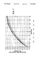
- FIG. 7 illustrates the absolute change in resistance with respect to temperature for the current shunt of the invention.
- a current shunt 10 of the type illustrated in FIG. 1 may introduce errors into the output measurement in that the potential contacts P 1 and P 2 are disposed in the current path between current contacts C 1 and C 2 .
- the current flow through current shunt 10 is illustrated in FIG. 2(a), where, as shown, the current flows through the potential contacts P 1 and P 2 .
- the present inventors have discovered that if an isolating structure is provided to prevent current flow in the body of the current shunt where the potential contact is made, both mechanical and temperature coefficient of resistance induced errors can be eliminated.
- the effective potential contact then becomes integral to the resistance element while the physical connection becomes part of the high impedance potential circuit where variations in contact quality have no impact on accuracy.
- the potential contact is designed to have isolating structures in the sheet portion of the current shunt so that the effective potential contact is made in the sheet material itself. As shown in FIG. 2(b), this may be done by placing slits in the sheet material to isolate the copper contact pin (P 1 or P 2 ) from the current path. Consequently, none of the potential drop occurs in the vicinity of the contact pin or the weld "nugget" where mixing of copper with the resistance alloy produces uncertain properties.
- the current path through the current shunt 20 (FIG. 2(b)) of the invention does not include the potential contacts P 1 and P 2 as in the prior art current shunt 10 of FIG. 2(a) and thus does not introduce the aforementioned errors into the output measurement.
- FIGS. 3(a) and 3(b) illustrate the current shunt 20 of the invention in which the current flow does not pass through the potential contacts P 1 and P 2 .
- the effective potential contacts are in the sheet material itself, the physical potential contacts P 1 and P 2 are effectively isolated from the current path so as to avoid any performance uncertainty caused by the presence of dissimilar metals at the junction between the physical terminal and the resistance element.
- this potential contact isolation is generally provided by forming slits between the current and potential contacts.
- FIG. 4 illustrates a presently preferred embodiment of the current shunt of the invention.
- FIG. 4(a) illustrates the current shunt of the invention while it is still in sheet form before being bent for mounting
- FIG. 4(b) illustrates an end view of the sheet of FIG. 4(a) after it has been bent for mounting.
- FIG. 4(c) illustrates a side view of the bent sheet of FIG. 4(a)
- FIG. 4(d) illustrates a top view of the bent sheet of FIG. 4(a).
- the current shunt 20 of FIGS. 4(a)-(d) preferably has slits 40 for isolating the potential contacts P 1 and P 2 from the current contacts C 1 and C 2 for the reasons described above with respect to FIGS. 2 and 3.
- the current shunt 20 of FIGS. 4(a)-(d) is further characterized by trimming and current diverting slits 42, integral heat sink (or "wings") 44 and strain relief slits 46.
- the potential and current contact pins are preferably welded at 48 to the current shunt 20 of the invention in accordance with known fusion welding techniques.
- the current shunt is also bent at 49 as illustrated prior to mounting so as to maximize surface area for cooling purposes and to facilitate mounting.
- Slit trimming of resistive devices is a well established technique frequently used when the resistive element is a thin film or foil.
- the fabricator compensates for variations in thickness and resistivity by trimming the film or foil.
- a fixed overall dimension for the device is maintained while trimming for virtually any desired level of accuracy at the device terminals.
- such techniques have not previously been used for resistive materials of the type used in the manufacture of current shunts. Instead, techniques such as grinding of the edges of the materials have been used to trim prior art current shunts, which is labor intensive and difficult to repeat exactly.
- the present inventors have extended the technique of slit trimming to bulk materials (i.e., 0.020" thick sheets) for adjusting the resistance of the sheet to a desired value, thereby compensating for resistance variation caused by variations in the thickness of the sheet and the like which occur during its manufacture.
- This makes it unnecessary to accurately control the thickness of the sheet during manufacture of the current shunt of the invention.
- the trimming and current diverting slits 42 are formed within the body of the current shunt 20 during manufacture.
- current shunt 20 is not individually trimmed; instead, unavoidable variability in the electrical and mechanical properties of the sheet material from lot to lot is adjusted to a nominal value by deliberately incorporating trimming and current diverting slits 42 rather than redesigning the current shunt 20.
- the size of the trimming and current diverting slits 42 may vary with each lot of material depending upon the resistive characteristics of the particular lot. The trimming and current diverting slits 42 raise the effective resistance of the current shunt 20 when low resistivity material is used and can be gradually eliminated to hold tolerance for absolute resistance when higher resistivity material is used.
- the current shunt 20 of the invention would have approximately a +/-20% tolerance of absolute resistance.
- tolerances better than +/-5% have been obtained.
- the trimming and current diverting slits 42 also provide another novel function in accordance with the invention.
- the trimming and current diverting slits 42 force the current flow into certain portions of the current shunt 20.
- This feature of the trimming and current diverting slits 42 may be used to direct the current to, for example, an integral heat sink (or "wings") 44 of the current shunt 20 for purposes of more efficiently dissipating heat.
- wings integral heat sink
- improved thermal performance may be achieved by providing the resistance sheet material with an integral heat sink 44.
- an integral heat sink 44 As known to those skilled in the art, one of the concerns in the design of any high current shunt is power dissipation which leads to both temperature coefficient of resistance and thermal EMF effects. Unfortunately, simply attaching a heat sink to the current shunt introduces various other effects which compromise shunt performance in complex and not well understood ways. These effects include strain, introduction of high impedance parallel current paths, and the like. Adding a heat sink also makes the manufacturing process more complex and adds cost to the device. In order to avoid these problems, the higher current versions of current shunt 20 in accordance with the invention preferably include integral "wings" 44 of the sheet material itself to increase surface area and to improve thermal performance. Those skilled in the art will appreciate that integral heat sinks 44 are not necessary for all designs but only for devices exhibiting relatively high power dissipations.
- the current shunt 20 in accordance with the invention is primarily cooled by convection aided by forced air
- the current shunt 20 of the invention has been designed to maintain a surface area to power dissipation ratio of roughly 0.5 Watts per square inch.
- some portion of the dissipation of heat is also conducted out the leads of the device into a circuit board on which the device is mounted.
- two trimming and current diverting slits 42 may also be provided to have the aforementioned function of forcing current flow up into the "wing" structures 44 in order to locate a greater portion of the dissipation more advantageously relative to an anticipated flow of cooling air, thereby improving thermal performance.
- Thermal performance is further improved in that a junction of dissimilar metals at the connection to the heat sink is not necessary.
- strain relief slits 46 within the "wings" 44 along the long axis parallel to the mounting direction for purposes of avoiding the compressive stresses caused by thermal expansion.
- strain relief may also be achieved by bending the sheet material in a direction perpendicular to the long axis direction in the mounting direction so as to avoid the compressive stresses caused by thermal expansion. In this manner, mechanical strain caused by temperature expansion may be minimized so as to enhance the stability of the resistance value with respect to time and temperature.
- the present invention also uses welded contacts for the current and potential connections. While welding technology has been used by some manufacturers of wire wound resistors including four-terminal current shunts, isolated welded contacts on a sheet resistance material (as opposed to ribbon material used in a wound-on-a-body type configuration) are not known in the prior art. Instead, prior art current shunts typically have either soft-soldered or silver-soldered current and potential connections which introduce the problems with dissimilar junctions noted above.
- the present invention provides numerous benefits including: (1) the contacts are mechanically stable; (2) the physical size of the contact may be more precisely controlled and in the case of the potential contacts is typically smaller than a soldered contact; (3) the thermally effected zone in the resistance element may be small if fusion welding techniques are used as opposed to soldering, brazing or other welding techniques; and (4) if solderable pins are welded to the device, the resulting component is compatible with volume manufacturing technologies such as wave soldering.
- the first three of these benefits contribute to improved performance in the finished device, while the fourth benefit improves the cost effectiveness of the current shunt of the invention.
- prior art current shunts are typically formed of alloys of materials such as manganin and constantan
- the present inventors have discovered that desirable results are achieved when the current shunt 20 is formed of an EvanohmTM S resistance alloy.
- Such a resistance alloy is presently preferred since it provides optimum stability and flexibility with regard to both size and required temperature coefficient of resistance.
- This alloy also has an extremely low EMF versus copper together with a high electrical resistivity as is highly desirable in a precision resistance element.
- the EvanohmTM S resistance alloy is generally formed of nickel and chromium and is typically used in strain gauges and precision foil resistors.
- the alloy used in a preferred embodiment of the invention has the following nominal composition: nickel 72%, chromium 20%, aluminum 3%, manganese 4% and silicon 1%.
- Such a material has a thermal coefficient of expansion of approximately 13.0 ⁇ 10 -6 °C. and a thermal conductivity of 0.146 W/cm/°C.
- such a material has a resistivity of approximately 825 ohms cir mil/ft and a thermal EMF versus copper of +0.2 microvolts/°C. (0°-100° C.). Since contact attachment to an alloy of this type has been found to be difficult, particularly for bulk materials on the order of 0.020" thickness, the aforementioned fusion welding technique has been developed in accordance with the invention.
- the material chosen for the resistance element of the invention preferably has a low temperature coefficient of resistance versus temperature as well as a low thermal EMF with respect to copper.
- stability of the current shunt of the invention may be enhanced by providing a stabilization bake of the current shunt after fabrication at a relatively low temperature such as 250° F. Accordingly, other similar materials may be used to achieve the benefits of the invention as would be apparent to those of ordinary skill in the art.
- FIGS. 5(a)-5(c) illustrate an alternative embodiment of the current shunt of the invention.
- current shunt 50 also has the slits 51 for isolating the potential contacts from the current contacts and trimming and current diverting slits 52 as well as welded connections 54 for connecting the current contacts and the potential contacts to the current shunt 50 as described above with respect to FIG. 4.
- the embodiment of FIG. 5 further includes transverse bends 56 for providing strain relief rather than the slits 46 as in the embodiment of FIG. 4.
- the sheet material is preferably folded into a "top hat" design before mounting by bending the resistive sheet along the long mounting axis to avoid compression stresses caused by thermal expansion with respect to the mounting points.
- FIGS. 6(a)-6(c) illustrate another embodiment for lower power usage which is very similar to that of FIG. 5.
- current shunt 60 includes isolating slits 61, trimming and current diverting slits 62, welded contacts 64 and bends 66 as in the embodiment of FIG. 5.
- a single pair of current connections C 1 and C 2 and a single pair of potential connections P 1 and P 2 are provided and less heat sinking is available.
- this embodiment maximizes the surface area of the resistive element without changing the resistance value of the overall current shunt and is bent so as to minimize strain due to thermal expansion.
- a "top hat" shape is presently preferred for this purpose.
- FIG. 7 illustrates resistance stability versus temperature for the current shunt of the invention.
- FIG. 7 illustrates deviation from a nominal resistance value as the current shunt is repeatedly heated from 0° C. to 80° C. and then cooled back to 0° C. for measuring hysteresis effects.
- minimal change in resistance for changes in temperature are measured for the current shunt of the invention.
Abstract
Description
Claims (10)
Priority Applications (2)
| Application Number | Priority Date | Filing Date | Title |
|---|---|---|---|
| US07/788,404 US5214407A (en) | 1991-11-06 | 1991-11-06 | High performance current shunt |
| JP29704092A JP3148415B2 (en) | 1991-11-06 | 1992-11-06 | High performance shunt |
Applications Claiming Priority (1)
| Application Number | Priority Date | Filing Date | Title |
|---|---|---|---|
| US07/788,404 US5214407A (en) | 1991-11-06 | 1991-11-06 | High performance current shunt |
Publications (1)
| Publication Number | Publication Date |
|---|---|
| US5214407A true US5214407A (en) | 1993-05-25 |
Family
ID=25144387
Family Applications (1)
| Application Number | Title | Priority Date | Filing Date |
|---|---|---|---|
| US07/788,404 Expired - Lifetime US5214407A (en) | 1991-11-06 | 1991-11-06 | High performance current shunt |
Country Status (2)
| Country | Link |
|---|---|
| US (1) | US5214407A (en) |
| JP (1) | JP3148415B2 (en) |
Cited By (35)
| Publication number | Priority date | Publication date | Assignee | Title |
|---|---|---|---|---|
| US5841272A (en) * | 1995-12-20 | 1998-11-24 | Sundstrand Corporation | Frequency-insensitive current sensor |
| US5917401A (en) * | 1997-02-26 | 1999-06-29 | Sundstrand Corporation | Conductive bus member and method of fabricating same |
| US6181234B1 (en) * | 1999-12-29 | 2001-01-30 | Vishay Dale Electronics, Inc. | Monolithic heat sinking resistor |
| EP1108260A1 (en) * | 1999-06-30 | 2001-06-20 | General Electric Company | Dual-rated current transformer circuit |
| EP1278069A1 (en) * | 2001-07-20 | 2003-01-22 | ENSECO GmbH | Low ohmic measuring resistor |
| US20030038706A1 (en) * | 2001-08-22 | 2003-02-27 | Kinya Nakatsu | Power converter with shunt resistor |
| US20030146077A1 (en) * | 2001-01-15 | 2003-08-07 | Hideki Enomoto | Shunt resistance and method of adjusting the shunt resistance |
| EP1374364A1 (en) * | 2001-04-06 | 2004-01-02 | Microchip Technology Incorporated | Terminal assembly for battery |
| US6671945B2 (en) | 2001-01-19 | 2004-01-06 | Vishay Intertechnology, Inc. | Method for making a resistor using resistive foil |
| US6677850B2 (en) * | 1998-06-25 | 2004-01-13 | Sentec Ltd. | Layered current sensor |
| US6794985B2 (en) * | 2000-04-04 | 2004-09-21 | Koa Corporation | Low resistance value resistor |
| US20050046543A1 (en) * | 2003-08-28 | 2005-03-03 | Hetzler Ullrich U. | Low-impedance electrical resistor and process for the manufacture of such resistor |
| FR2879751A1 (en) * | 2004-12-20 | 2006-06-23 | Johnson Controls Tech Co | DEVICE FOR MEASURING CIRCULATING CURRENT IN A CABLE |
| DE102006039722A1 (en) * | 2006-08-24 | 2008-02-28 | Conti Temic Microelectronic Gmbh | Electrical component, in particular measuring resistor and method for producing such an electrical component |
| EP2012357A3 (en) * | 1998-12-09 | 2009-07-29 | Fuji Electric Company Limited | Method of manufacturing a semi conductor device |
| US20110310568A1 (en) * | 2010-06-21 | 2011-12-22 | Infineon Technologies Ag | Circuit Arrangement with Shunt Resistor |
| US8598976B2 (en) * | 2009-07-01 | 2013-12-03 | Isabellenhütte Heusler Gmbh & Co. Kg | Electronic component and corresponding production method |
| US20130328547A1 (en) * | 2011-12-23 | 2013-12-12 | Sendyne Corporation | Current Shunt |
| CN106093523A (en) * | 2016-06-21 | 2016-11-09 | 福建省计量科学研究院 | A kind of I V changer |
| US20170162302A1 (en) * | 2014-06-17 | 2017-06-08 | Koa Corporation | Current detection resistor |
| US20170271055A1 (en) * | 2016-03-18 | 2017-09-21 | Rohm Co., Ltd. | Shunt resistor |
| US20170317013A1 (en) * | 2016-04-28 | 2017-11-02 | Texas Instruments Incorporated | Shunt strip |
| US9934893B2 (en) * | 2015-04-28 | 2018-04-03 | Suncall Corporation | Shunt resistor and method for manufacturing same |
| WO2018158330A1 (en) * | 2017-03-03 | 2018-09-07 | Continental Automotive Gmbh | Current sensor with optimised current density distribution, and method for determining a load current |
| GB2568762A (en) * | 2017-11-28 | 2019-05-29 | Safran Electrical & Power | Aircraft power control device |
| EP3578997A1 (en) * | 2018-06-05 | 2019-12-11 | Yazaki Corporation | Current sensor |
| US10748679B2 (en) * | 2017-04-25 | 2020-08-18 | Yazaki Europe Limited | Power resistor |
| US10932367B2 (en) * | 2011-05-17 | 2021-02-23 | Rohm Co., Ltd. | Chip resistor, method of producing chip resistor and chip resistor packaging structure |
| US20220102032A1 (en) * | 2019-08-13 | 2022-03-31 | Lg Energy Solution, Ltd. | Shunt Resistor Module |
| US20220189664A1 (en) * | 2020-12-10 | 2022-06-16 | Wieland-Werke Ag | Resistor assembly and method for producing same |
| US20220254551A1 (en) * | 2019-11-18 | 2022-08-11 | Suncall Corporation | Shunt Resistor |
| US11488750B2 (en) * | 2015-10-15 | 2022-11-01 | Suncall Corporation | Shunt resistor |
| US11555831B2 (en) * | 2020-08-20 | 2023-01-17 | Vishay Dale Electronics, Llc | Resistors, current sense resistors, battery shunts, shunt resistors, and methods of making |
| US11562838B2 (en) | 2009-09-04 | 2023-01-24 | Vishay Dale Electronics, Llc | Resistor with temperature coefficient of resistance (TCR) compensation |
| US20230326633A1 (en) * | 2022-04-08 | 2023-10-12 | Cyntec Co., Ltd. | Structure of resistor device and system for measuring resistance of same |
Families Citing this family (3)
| Publication number | Priority date | Publication date | Assignee | Title |
|---|---|---|---|---|
| JP2000133501A (en) * | 1998-10-23 | 2000-05-12 | Matsushita Electric Ind Co Ltd | Resistor |
| JP5147370B2 (en) * | 2007-11-20 | 2013-02-20 | 三菱電機株式会社 | Servo motor control device |
| JP5840527B2 (en) * | 2012-02-21 | 2016-01-06 | 本田技研工業株式会社 | Circuit board |
Citations (4)
| Publication number | Priority date | Publication date | Assignee | Title |
|---|---|---|---|---|
| US3252091A (en) * | 1961-12-08 | 1966-05-17 | Electro Scient Ind Inc | Four-terminal junction for electrical measurments and method of making the same |
| US4475099A (en) * | 1983-06-27 | 1984-10-02 | Analogic Corporation | Voltage divider |
| US4973837A (en) * | 1986-08-13 | 1990-11-27 | Electrosense Limited | Proximity detectors with dual-speed tracking circuitry |
| US5015989A (en) * | 1989-07-28 | 1991-05-14 | Pacific Hybrid Microelectronics, Inc. | Film resistor with enhanced trimming characteristics |
-
1991
- 1991-11-06 US US07/788,404 patent/US5214407A/en not_active Expired - Lifetime
-
1992
- 1992-11-06 JP JP29704092A patent/JP3148415B2/en not_active Expired - Fee Related
Patent Citations (4)
| Publication number | Priority date | Publication date | Assignee | Title |
|---|---|---|---|---|
| US3252091A (en) * | 1961-12-08 | 1966-05-17 | Electro Scient Ind Inc | Four-terminal junction for electrical measurments and method of making the same |
| US4475099A (en) * | 1983-06-27 | 1984-10-02 | Analogic Corporation | Voltage divider |
| US4973837A (en) * | 1986-08-13 | 1990-11-27 | Electrosense Limited | Proximity detectors with dual-speed tracking circuitry |
| US5015989A (en) * | 1989-07-28 | 1991-05-14 | Pacific Hybrid Microelectronics, Inc. | Film resistor with enhanced trimming characteristics |
Cited By (60)
| Publication number | Priority date | Publication date | Assignee | Title |
|---|---|---|---|---|
| US5841272A (en) * | 1995-12-20 | 1998-11-24 | Sundstrand Corporation | Frequency-insensitive current sensor |
| US5917401A (en) * | 1997-02-26 | 1999-06-29 | Sundstrand Corporation | Conductive bus member and method of fabricating same |
| US6677850B2 (en) * | 1998-06-25 | 2004-01-13 | Sentec Ltd. | Layered current sensor |
| EP2012357A3 (en) * | 1998-12-09 | 2009-07-29 | Fuji Electric Company Limited | Method of manufacturing a semi conductor device |
| EP1108260A1 (en) * | 1999-06-30 | 2001-06-20 | General Electric Company | Dual-rated current transformer circuit |
| EP1108260A4 (en) * | 1999-06-30 | 2009-03-25 | Gen Electric | Dual-rated current transformer circuit |
| US6181234B1 (en) * | 1999-12-29 | 2001-01-30 | Vishay Dale Electronics, Inc. | Monolithic heat sinking resistor |
| US7042330B2 (en) | 2000-04-04 | 2006-05-09 | Koa Corporation | Low resistance value resistor |
| US6794985B2 (en) * | 2000-04-04 | 2004-09-21 | Koa Corporation | Low resistance value resistor |
| US20040196139A1 (en) * | 2000-04-04 | 2004-10-07 | Koa Corporation | Low resistance value resistor |
| US20030146077A1 (en) * | 2001-01-15 | 2003-08-07 | Hideki Enomoto | Shunt resistance and method of adjusting the shunt resistance |
| US7088217B2 (en) * | 2001-01-15 | 2006-08-08 | Matsushita Electric Works, Ltd. | Shunt resistance and method of adjusting the shunt resistance |
| US6671945B2 (en) | 2001-01-19 | 2004-01-06 | Vishay Intertechnology, Inc. | Method for making a resistor using resistive foil |
| US6680668B2 (en) * | 2001-01-19 | 2004-01-20 | Vishay Intertechnology, Inc. | Fast heat rise resistor using resistive foil |
| EP1374364A4 (en) * | 2001-04-06 | 2008-05-14 | Microchip Tech Inc | Terminal assembly for battery |
| EP1374364A1 (en) * | 2001-04-06 | 2004-01-02 | Microchip Technology Incorporated | Terminal assembly for battery |
| EP2256900A1 (en) * | 2001-04-06 | 2010-12-01 | Microchip Technology Incorporated | Terminal Assembly for a Battery |
| EP1278069A1 (en) * | 2001-07-20 | 2003-01-22 | ENSECO GmbH | Low ohmic measuring resistor |
| US6794854B2 (en) | 2001-08-22 | 2004-09-21 | Hitachi, Ltd. | Vehicle power converted with shunt resistor having plate-shape resistive member |
| US20030038706A1 (en) * | 2001-08-22 | 2003-02-27 | Kinya Nakatsu | Power converter with shunt resistor |
| US6960980B2 (en) * | 2001-08-22 | 2005-11-01 | Hitachi, Ltd. | Power converter with shunt resistor |
| US20050046543A1 (en) * | 2003-08-28 | 2005-03-03 | Hetzler Ullrich U. | Low-impedance electrical resistor and process for the manufacture of such resistor |
| US8242772B2 (en) | 2004-12-20 | 2012-08-14 | Johnson Controls Technology Company | Device for measuring a current flowing in a cable |
| US20100066351A1 (en) * | 2004-12-20 | 2010-03-18 | Johnson Controls Technology Company | Device for measuring a current flowing in a cable |
| WO2006067300A1 (en) * | 2004-12-20 | 2006-06-29 | Johnson Controls Technology Company | Device for measuring a current flowing in a cable |
| US20110062945A1 (en) * | 2004-12-20 | 2011-03-17 | Johnson Controls Technology Company | Device for measuring a current flowing in a cable |
| FR2879751A1 (en) * | 2004-12-20 | 2006-06-23 | Johnson Controls Tech Co | DEVICE FOR MEASURING CIRCULATING CURRENT IN A CABLE |
| US8142237B2 (en) | 2004-12-20 | 2012-03-27 | Johnson Controls Technology Company | Device for measuring a current flowing in a cable |
| DE102006039722A1 (en) * | 2006-08-24 | 2008-02-28 | Conti Temic Microelectronic Gmbh | Electrical component, in particular measuring resistor and method for producing such an electrical component |
| US8598976B2 (en) * | 2009-07-01 | 2013-12-03 | Isabellenhütte Heusler Gmbh & Co. Kg | Electronic component and corresponding production method |
| US11562838B2 (en) | 2009-09-04 | 2023-01-24 | Vishay Dale Electronics, Llc | Resistor with temperature coefficient of resistance (TCR) compensation |
| US20110310568A1 (en) * | 2010-06-21 | 2011-12-22 | Infineon Technologies Ag | Circuit Arrangement with Shunt Resistor |
| US9661752B2 (en) * | 2010-06-21 | 2017-05-23 | Infineon Technologies Ag | Circuit arrangement with shunt resistor |
| US11324121B2 (en) | 2011-05-17 | 2022-05-03 | Rohm Co., Ltd. | Chip resistor, method of producing chip resistor and chip resistor packaging structure |
| US10932367B2 (en) * | 2011-05-17 | 2021-02-23 | Rohm Co., Ltd. | Chip resistor, method of producing chip resistor and chip resistor packaging structure |
| US20130328547A1 (en) * | 2011-12-23 | 2013-12-12 | Sendyne Corporation | Current Shunt |
| US9217759B2 (en) * | 2011-12-23 | 2015-12-22 | Sendyne Corporation | Current shunt |
| US20170162302A1 (en) * | 2014-06-17 | 2017-06-08 | Koa Corporation | Current detection resistor |
| US9934893B2 (en) * | 2015-04-28 | 2018-04-03 | Suncall Corporation | Shunt resistor and method for manufacturing same |
| US11488750B2 (en) * | 2015-10-15 | 2022-11-01 | Suncall Corporation | Shunt resistor |
| US20170271055A1 (en) * | 2016-03-18 | 2017-09-21 | Rohm Co., Ltd. | Shunt resistor |
| US9966170B2 (en) * | 2016-03-18 | 2018-05-08 | Rohm Co., Ltd. | Shunt resistor |
| US10739383B2 (en) | 2016-04-28 | 2020-08-11 | Texas Instruments Incorporated | Shunt strip |
| US20170317013A1 (en) * | 2016-04-28 | 2017-11-02 | Texas Instruments Incorporated | Shunt strip |
| US10365303B2 (en) * | 2016-04-28 | 2019-07-30 | Texas Instruments Incorporated | Shunt strip |
| CN106093523A (en) * | 2016-06-21 | 2016-11-09 | 福建省计量科学研究院 | A kind of I V changer |
| US11156643B2 (en) | 2017-03-03 | 2021-10-26 | Continental Automotive Gmbh | Current sensor with optimized current density distribution, method for determining a load current |
| WO2018158330A1 (en) * | 2017-03-03 | 2018-09-07 | Continental Automotive Gmbh | Current sensor with optimised current density distribution, and method for determining a load current |
| US10748679B2 (en) * | 2017-04-25 | 2020-08-18 | Yazaki Europe Limited | Power resistor |
| GB2568762A (en) * | 2017-11-28 | 2019-05-29 | Safran Electrical & Power | Aircraft power control device |
| GB2568762B (en) * | 2017-11-28 | 2022-01-19 | Safran Electrical & Power | Aircraft power control device |
| EP3578997A1 (en) * | 2018-06-05 | 2019-12-11 | Yazaki Corporation | Current sensor |
| US20220102032A1 (en) * | 2019-08-13 | 2022-03-31 | Lg Energy Solution, Ltd. | Shunt Resistor Module |
| US11961642B2 (en) * | 2019-08-13 | 2024-04-16 | Lg Energy Solution, Ltd. | Shunt resistor module |
| US20220254551A1 (en) * | 2019-11-18 | 2022-08-11 | Suncall Corporation | Shunt Resistor |
| US11555831B2 (en) * | 2020-08-20 | 2023-01-17 | Vishay Dale Electronics, Llc | Resistors, current sense resistors, battery shunts, shunt resistors, and methods of making |
| US20230341440A1 (en) * | 2020-08-20 | 2023-10-26 | Vishay Dale Electronics, Llc | Resistors, current sense resistors, battery shunts, shunt resistors, and methods of making |
| US20220189664A1 (en) * | 2020-12-10 | 2022-06-16 | Wieland-Werke Ag | Resistor assembly and method for producing same |
| US11621107B2 (en) * | 2020-12-10 | 2023-04-04 | Wieland-Werke Ag | Resistor assembly and method for producing same |
| US20230326633A1 (en) * | 2022-04-08 | 2023-10-12 | Cyntec Co., Ltd. | Structure of resistor device and system for measuring resistance of same |
Also Published As
| Publication number | Publication date |
|---|---|
| JP3148415B2 (en) | 2001-03-19 |
| JPH05223850A (en) | 1993-09-03 |
Similar Documents
| Publication | Publication Date | Title |
|---|---|---|
| US5214407A (en) | High performance current shunt | |
| US8319499B2 (en) | Coated motor vehicle battery sensor element and method for producing a motor vehicle battery sensor element | |
| US4200970A (en) | Method of adjusting resistance of a thermistor | |
| EP1028436B1 (en) | Resistor and method for manufacturing the same | |
| US8581687B2 (en) | Four-terminal resistor with four resistors and adjustable temperature coefficient of resistance | |
| USRE39660E1 (en) | Surface mounted four terminal resistor | |
| US9217759B2 (en) | Current shunt | |
| US8129228B2 (en) | Manufacturing method for integrating a shunt resistor into a semiconductor package | |
| JP2002057009A (en) | Resistor and method of manufacturing the same | |
| US9429967B2 (en) | High precision resistor and trimming method thereof | |
| US5057811A (en) | Electrothermal sensor | |
| US7385828B2 (en) | Electronic shunt resistor assembly | |
| US8324721B2 (en) | Integrated shunt resistor with external contact in a semiconductor package | |
| EP4145472A1 (en) | Current detection device | |
| US6292091B1 (en) | Resistor and method of adjusting resistance of the same | |
| EP2169412A1 (en) | Electrical current measurement arrangement | |
| JP4056445B2 (en) | Metal resistor | |
| JP2002184601A (en) | Resistor unit | |
| JP2006112868A (en) | Resistor for current detection | |
| US20030089964A1 (en) | Surge current chip resistor | |
| JP3670593B2 (en) | Electronic component using resistor and method of using the same | |
| KR19990028577A (en) | Shunt assembly for current measurement | |
| JP2002050501A (en) | Mounting body and using method thereof | |
| US5361634A (en) | Heat-sensitive flow rate sensor | |
| JP2002057010A (en) | Resistor and method of manufacturing the same |
Legal Events
| Date | Code | Title | Description |
|---|---|---|---|
| AS | Assignment |
Owner name: HEWLETT-PACKARD COMPANY, CALIFORNIA Free format text: ASSIGNMENT OF ASSIGNORS INTEREST.;ASSIGNORS:MCKIM, JAMES B. JR.;PECK, ROBERT D.;MYERS, RICHARD S.;AND OTHERS;REEL/FRAME:006369/0298 Effective date: 19911118 |
|
| STCF | Information on status: patent grant |
Free format text: PATENTED CASE |
|
| FEPP | Fee payment procedure |
Free format text: PAYOR NUMBER ASSIGNED (ORIGINAL EVENT CODE: ASPN); ENTITY STATUS OF PATENT OWNER: LARGE ENTITY |
|
| FPAY | Fee payment |
Year of fee payment: 4 |
|
| AS | Assignment |
Owner name: HEWLETT-PACKARD COMPANY, A DELAWARE CORPORATION, C Free format text: MERGER;ASSIGNOR:HEWLETT-PACKARD COMPANY, A CALIFORNIA CORPORATION;REEL/FRAME:010841/0649 Effective date: 19980520 |
|
| AS | Assignment |
Owner name: AGILENT TECHNOLOGIES INC., CALIFORNIA Free format text: ASSIGNMENT OF ASSIGNORS INTEREST;ASSIGNOR:HEWLETT-PACKARD COMPANY, A DELAWARE CORPORATION;REEL/FRAME:010901/0336 Effective date: 20000520 |
|
| FPAY | Fee payment |
Year of fee payment: 8 |
|
| FPAY | Fee payment |
Year of fee payment: 12 |