US5157698A - Method for clock pulse synchronization - Google Patents

Method for clock pulse synchronization Download PDF

Info

Publication number
US5157698A
US5157698A US07/423,404 US42340489A US5157698A US 5157698 A US5157698 A US 5157698A US 42340489 A US42340489 A US 42340489A US 5157698 A US5157698 A US 5157698A
Authority
US
United States
Prior art keywords
phase
received signal
signal
value
complex
Prior art date
Legal status (The legal status is an assumption and is not a legal conclusion. Google has not performed a legal analysis and makes no representation as to the accuracy of the status listed.)
Expired - Fee Related
Application number
US07/423,404
Inventor
Volker Hespelt
Thomas Alberty
Current Assignee (The listed assignees may be inaccurate. Google has not performed a legal analysis and makes no representation or warranty as to the accuracy of the list.)
Bosch Telecom GmbH
Original Assignee
ANT Nachrichtentechnik GmbH
Priority date (The priority date is an assumption and is not a legal conclusion. Google has not performed a legal analysis and makes no representation as to the accuracy of the date listed.)
Filing date
Publication date
Application filed by ANT Nachrichtentechnik GmbH filed Critical ANT Nachrichtentechnik GmbH
Assigned to ANT NACHRICHTENTECHNIK GMBH reassignment ANT NACHRICHTENTECHNIK GMBH ASSIGNMENT OF ASSIGNORS INTEREST. Assignors: ALBERTY, THOMAS, HESPELT, VOLKER
Application granted granted Critical
Publication of US5157698A publication Critical patent/US5157698A/en
Anticipated expiration legal-status Critical
Expired - Fee Related legal-status Critical Current

Links

Images

Classifications

    • HELECTRICITY
    • H04ELECTRIC COMMUNICATION TECHNIQUE
    • H04LTRANSMISSION OF DIGITAL INFORMATION, e.g. TELEGRAPHIC COMMUNICATION
    • H04L7/00Arrangements for synchronising receiver with transmitter
    • H04L7/0054Detection of the synchronisation error by features other than the received signal transition
    • HELECTRICITY
    • H04ELECTRIC COMMUNICATION TECHNIQUE
    • H04LTRANSMISSION OF DIGITAL INFORMATION, e.g. TELEGRAPHIC COMMUNICATION
    • H04L7/00Arrangements for synchronising receiver with transmitter
    • H04L7/02Speed or phase control by the received code signals, the signals containing no special synchronisation information
    • H04L7/027Speed or phase control by the received code signals, the signals containing no special synchronisation information extracting the synchronising or clock signal from the received signal spectrum, e.g. by using a resonant or bandpass circuit

Landscapes

  • Engineering & Computer Science (AREA)
  • Computer Networks & Wireless Communication (AREA)
  • Signal Processing (AREA)
  • Digital Transmission Methods That Use Modulated Carrier Waves (AREA)
  • Synchronisation In Digital Transmission Systems (AREA)

Abstract

A method of synchronizing clock pulses of a clock pulse generator used in a receiver of digital data transmissions. The received signal is demodulated by multiplying it in quadrature by an output signal of a carrier oscillator to obtain demodulated in-phase and quadrature components. The demodulated components are lowpass filtered to suppress harmonics of the carrier frequency and then bandpass filtered into two complex signals. The two complex signals are then linked together with a first linkage circuit to form a first control signal uTI. The two complex signals are also linked together with a second linkage circuit to form a second control uTR, wherein the two control signals can be interpretated as the real and imaginary components of a complex control signal uT =uTR +juTI. The two components are separately averaged and then evaluated to form an actuation signal having an actuation value δ representing an error in the timing of the error pulse generator relative to the received signal. The evaluation is based on the relationship φ=arc tan uTI /uTR, where φ is the phase error in the clock pulse relative to the received signal.

Description

BACKGROUND OF THE INVENTION
The invention relates to a method and to a circuit arrangement for implementing a synchronization method in a receiver of digital data transmissions including a timing error detector to which are fed in in-phase component and a quadrature component of a demodulated received signal produced from products of the received signal and an output signal of a carrier oscillator and lowpass filtering of the products to suppress harmonics. An output signal of the timing error detector serves as a control signal uTI for a clock pulse generator which produces clock pulses for sampling the received signal. The control signal uTI is produced by means of two bandpass filters in the timing error detector which convert the demodulated received signal into two respective complex signals which are in turn linked together by means of a linkage circuit in the timing error detector to form the control signal uTI. The control signal uTI is used to actuate a timing error correction circuit of the clock pulse generator to synchronize the clock pulses with the received signal.
Such methods are known, for example from the article by Gardner, entitled "A BPSK/QPSK Timing-Error Detector for Sampled Receivers," in IEEE Com.-34, No. 5, May, 1986, pages 423-429.
In digital data transmission it is important for the receiver to derive the exact sampling moment from the received data. For this purpose, a timing error detector generates by way of non-linear operations an output signal uTI whose fundamental mode corresponds to the clock pulse frequency and whose zero passages permit derivation of the sampling moment.
FIG. 1 shows a clock pulse control loop as disclosed in the above Gardner article and as it is employed, for example, for QPSK (quadrature phase shift keyed) data transmission. The incoming received signal s(t) is demodulated in that the carrier signal is fed to it multiplicatively once directly and once with a phase shift of -π/2. By means of lowpass filters TP, the products of the double frequency are suppressed. The normal component, i.e. the real component x(t), and the quadrature component, i.e. the imaginary component y(t), of the demodulated input signal are obtained from the outputs of the lowpass filters and fed to a subsequent timing error detector TD. Its output signal uTI is fed via a loop filter (SF) to a timing error correction device TPK which actuates a sampling device A for sampling, for example, the non-demodulated or the demodulated input signal. Such sampling is necessary if the signals are to be processed in the receiver in a time discrete manner.
In FIG. 1, for example, sampling occurs before demodulation. However, such sampling could also be done at any other desired location, for example after demodulation or after lowpass filtering. It is here assumed that the output signal of the timing error detector is present as a sampled signal uTI (kT), where T is the symbol interval or the step length which, according to the relationship of fNyq =1/2T is a function of the Nyquist frequency fNyq. The sampling phase of the sampler A present in the receiver is changed by way of loop filter SF and timing error correction circuit TPK until the sampled values at the output of the timing error detector average zero: uTI (k·T)=0, where k is an integer which numbers the clock pulses.
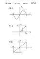
FIG. 2 shows the typical characteristic of a timing error detector. The sampling phase ε , i.e. the deviation Δt/T of the actual sampling moments from the correct sampling moments (in the case where transmitter and receiver clock pulse are coherent, ε=0) are plotted in the direction of the abscissa and the averages of uTI are plotted in the direction of the ordinate. For ε=0 and ε=±0.5, uTI =0. The center ε=0 of this sinusoidal curve is stable while at ε=±0.5, synchronization may be labile, i.e. it is possible that the synchronization is caught at the labile point for a longer or shorter period of time, thus noticeably lengthening the synchronization time.
SUMMARY OF THE INVENTION
It is the object of the present invention to provide a method of the above-mentioned type which is able to substantially suppress the above-described getting-caught and permits much faster synchronization.
The solution is effected as follows: By means of a second linkage circuit in the timing error detector, the two complex signals from the bandpass filters are linked together to form a second control signal uTR in such a manner that the two control signals uTR and uTI can be interpreted as the real component and the imaginary component of a complex control value uT =uTR +juTI. The two control signals uTR and uTI are subjected to averaging. Thereafter, the thus averaged values uTR and uTI are evaluated by means of an evaluation circuit to form an actuation value δ which actuates the timing error correction circuit.
The method according to the invention has the advantage that the above-described getting-caught is substantially suppressed and thus synchronization can take place much faster. The additional costs for this are relatively low.
BRIEF DESCRIPTION OF THE DRAWINGS
FIG. 1 is a block circuit diagram of a clock pulse control loop according to the prior art;
FIG. 2 shows a graph of a characteristic of an output signal of a timing error detector;
FIG. 3 is a plot of averages of real and imaginary components of a complex timing error detector output signal;
FIG. 4 is a plot of the phase angle of a complex timing error detector output vector as a function of the sampling phase;
FIG. 5 is a block diagram of a circuit for carrying out a method of synchronizing clock pulses according to an embodiment of the invention;
FIG. 5a is a block diagram of the timing error detection circuit;
FIG. 5b in a block diagram of the linkage circuit, of the timing error detector circuit, for producing the real component uTR of the complex control value uT ;
FIG. 5c is a block diagram of the linkage circuit, of the timing error detector circuit, for producing the imaginary component uTI of the complex control value uT ;
FIG. 6 is a block diagram of a circuit for carrying out a second embodiment of the method of the invention;
FIGS. 7a-7f, 8a and 8b are plots illustrating several ways of evaluating the averaged values uTR, uTI ; and
FIG. 9 illustrates a circuit arrangement for carrying out a still further embodiment of the method of the invention.
DESCRIPTION OF THE PREFERRED EMBODIMENTS
Applicant's German Application P 37 07 763 (corresponding to applicant's allowed copending U.S. application Ser. No. 07/423,391, filed Sept. 11, 1989) now U.S. Pat. No. 5,031,199 issued Jul. 9, 1991. discloses combined frequency and timing error detectors in which the timing error detector generates two output signals uTR and uTI which can be interpreted as the real and the imaginary component of a complex timing error detector output signal uT =uTR +juTI. Details of the timing error detector are described below. If one plots the average of uTR and uTI as the real component and the imaginary component in a complex plane, a complex vector of a length ρ=√uTR 2 +uTI 2 and the phase angle φ=arc tan uTI /uTR results, see FIG. 3.
The use of φ=arc tan uTI /uTR as the actuation signal for the subsequent timing error correction circuit leads to improved acquisition behavior. The relationship between ε and φ is shown in FIG. 4.
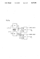
The method according to the invention will now be described with reference to FIG. 5 which shows an arrangement according to the invention. The real component uTR and the imaginary component uTI of the clock pulse oscillation are generated with the aid of a timing error detector TD, as disclosed in the above identified German application and in the corresponding U.S. Pat. No. 5,031,197 and illustrated in FIGS. 5a, 5b and 5c as described below. As is illustrated in FIG. 5a, the timing error detector TD includes two bandpass filters BP+ and two combining or linkage circuits VTR and VTI. The two bandpass filters BP+ respectively bandpass filter the lowpass filtered demodulated in-phase component x and quadrature component y or a received signal, to obtain two respective complex signals (rx)+j(iy) and (ry)+(j(iy), where j+√-1, rx and ry are real components and ix and iy are imaginary components. The linkage circuits VTR and VTI link the two complex signals in different ways to produce the output signals uTR and uTI as respectively illustrated in FIGS. 5b and 5c. As shown in FIG. 5b, linkage circuit VTR squares the respective components rx, ry, ix and iy and then combines the squared components to obtain uTR =(rx)2 +(iy)2 -(ix)2 -(iy)2, and as shown in FIG. 5c, multiples the components in pairs, to obtain the products (rx)(ix) and (ry)(iy), sums the products the and multiplies the sum by 2 to obtain uTI 2{(rx)(ix)+(ry)(iy)}.
The real component and imaginary component should be present either as samples uTR (k·T), uTI (K·T) or they are sampled at the sampling rate fS =1/T, with the sampling phase or, more precisely, its deviation, being assumed to be ε=Δt/T. Such a sampling of the two output signals of timing error detector TD is shown in FIG. 5. The samples of the two components are then averaged over m clock pulses in average formers MW. In special cases, m=1, i.e. no averaging is possible. After an averaging time of m·T, the averages are fed to an evaluation circuit AS which feeds an adjustment or control information δ to the subsequent timing error correction circuit TPK. The latter, in turn, puts out the sampling clock pulse at a sampling phase corrected by δ.
The function of evaluation circuit AS will be described with reference to FIGS. 7a-7f, 8a and 8b. These figures show several possibilities for evaluating the two averages.
A first possible way is shown in FIGS. 7a and 7b. The phase φ=arc tan uTI /uTR is formed from the two averages uTR and uTI. A linear relationship of δ=0.5·φπ exists between the phase φ and δ as shown in FIG. 7b. The precise determination of phase φ is somewhat complicated. It is simplified if regions are formed in the uTR, uTI plane which are easily queried and fixed phase values φQ are then assigned to these regions.
This second possible way is shown in FIGS. 7c and 7d. In FIG. 7c, a vector is assigned to each hatched region identified by encircled numerals, with the respective vector bearing the same numeral. The asterisks identify the tips of the respective vector. Thus each region has associated with it as φQ the phase of the corresponding vector. This corresponds to quantizing of φ as shown in FIG. 7d. The linear relationship between δ and φ according to FIG. 7a thus changes to a stepped curve as shown in FIG. 7d in which the following applies: δ=0.5·φQ /π and which shows the association of the regions with the fixed phase values of the table below. The division into regions shown in FIG. 7c is merely an example. Other types of regional divisions may of course also be realized; they differ in the magnitude of the expenditures for the query logic.
              TABLE                                                       
______________________________________                                    
Phase angle region of φ.sup.--                                        
                        φ.sub.Q                                       
______________________________________                                    
-π/16 ≧ φ.sup.--  ≦ + π/16                        
                        0                                                 
π/16 < φ.sup.--  ≦ π/4                                   
                        π/16                                           
π/4 < φ.sup.--  ≦ π/2                                    
                        π/4                                            
π/2 < φ.sup.--  ≦ π                                      
                        3π/4                                           
-π/16 > φ.sup.-- -π/16. -π/4                                 
-π/4 > φ.sup.--  ≧ -π/2                                  
                        -π/4                                           
-π/2 > φ.sup.--  > -π                                           
                        -3π/4                                          
______________________________________                                    
A third possible way shown in FIGS. 7e and 7f is very inexpensive. Here the quantized value φQmin is fixed for positive phases φ and the quantized value φQ =-φmin is fixed for negative phases φ, so that δ=±δmin =±0.5·φmin /π. Thus, in this manner of proceeding, only the sign of imaginary component uTI is evaluated and the actuation value δ is realized according to the equation δ=δmin ·sign(uTI). However, in this very simple procedure, the problem of the timing control being caught occurs again, namely at a sampling error of ±50%. The problem can be prevented by the evaluation shown in FIGS. 8a and 8b . The quantization characteristic according to FIG. 8b includes a hysteresis in phase regions π/2<φ<3φ/2 and -3φ/2<φ<-π/2, respectively, while region -π/2 ≦φ ≦φ/2 corresponds precisely to the corresponding region of the quantization characteristic of FIG. 7f. The use of a hysteresis is made possible, for example, in that the region of the complex uTR, uTI plane is divided into three regions, namely the first quadrant, the fourth quadrant and a region covering the second and third quadrants, i.e. for negative uTR values. A phase value assignment of +φmin applies for the first quadrant and a phase value assignment of -φmin for the fourth quadrant. The second and third quadrants receive phase value assignments of ±α·φmin, where α≧1. However, the assignments are made in such a way that if phase φ is enlarged out of the first quadrant, the assignment will continue with a positive value +φmin or >+min and only if the phase changes from the third into the fourth quadrant, is the phase value of -φmin assigned which is applicable there. Conversely, if phase φ becomes smaller and changes, for example, from the fourth quadrant to the third and second quadrants, the phase value of -φmin assigned to the fourth quadrant is retained or reduced further (α>1). Only if a change should occur from the second to the first quadrant, is the new phase value +φmin existing there assigned again. Thus, the actuation value δ is assigned according to the equation δ+0.5 sgn (uTI). φmin /π if sgn (uTR) is positive, and according to the equation δ=0.5 sgn (uTIP)·α·φmin /π if sgn (uTR) is negative, wherein α≧1 and sgn (uTIP) is the sign of uTI at a most recent time that uTR was positive. The division into regions and the assignment of phase values can be seen in FIG. 8a. Of course, another regional division may be realized as well. The regional assignment shown here, however, is particularly inexpensive; it merely necessitates a query for the second and third quadrants whether the real component of the average of the timing error detector output signal is negative.
According to FIG. 5, the real and imaginary components of the complex output signal of timing error detector TD are sampled at intervals of a step length T, i.e. at the clock pulse rate fS =1/T.
FIG. 6 shows an arrangement in which averaging is performed analogously, e.g. by means of lowpass filters. The sampling here does not take place until downstream of the average formers and at the reduced sampling rate fS /m. The requirements for the subsequent analog-digital conversion are thus reduced as well. In contrast to FIG. 5, the block circuit diagram of FIG. 6 shows a demodulator module DEM included between timing error detector TD and average formers MW, with fT being the clock pulse frequency.
Basically, two possibilities exist to correct the sampling moment: firstly by way of a feedback arrangement and secondly by an arrangement for forward correction.
The first is shown in FIG. 1. The feedback arrangement is distinguished in that the timing error detector is influenced by the corrected sampling phase itself. If the sampling phase is correct, the output signal of the timing error detector will average zero.
An arrangement for forward correction is shown in FIG. 9. Here, the output signal of timing error detector TD is influenced not by the correction of the sampling phase, rather the output signal of timing error correction circuit TPK is utilized only to set the sampling phase A in the data signal branch.
The arrangements of FIGS. 5 and 6 permit many possible combinations of averaging duration m·T and evaluation circuit AS.
Both arrangements and their combinations can be utilized for the timing control according to FIG. 1 and also for the forward timing control of FIG. 9.
In a feedback arrangement according to FIG. 1 it is favorable to select m to be small, e.g. m=1, and to perform only a rough quantization of the sampling phase in evaluation circuit AS in any of the ways described above with reference to FIGS. 7c-7f, 8a and 8b.
The costs for realization will then become correspondingly low.
For the forward correction of the clock pulse shown in FIG. 9, however, wherein the signal s(t) is applied to a demodulator Dem and a preequalizer VE before being sampled according to the output of timing error circuit TPK, it is necessary foe the evaluation circuit AS to furnish the most accurate possible linear estimate of the sampling phase. This is the case if, in the circuit arrangement according to FIG. 5 or 6, the averaging time m·T is large, i.e. m is high, and in evaluation circuit AS phase φ is determined as accurately as possible, e.g. by effecting the evaluation according to the equation δ=0.5·φ/π, where φ=arc tan uTI /uTR, as illustrated in FIGS. 7a and 7b.

Claims (15)

We claim:
1. A method of synchronizing clock pulses of a clock pulse generator in a receiver of digital data transmissions with a received signal, the clock pulses to be applied in sampling the received signal, the method comprising the steps of:
multiplying the received signal in-phase and in quadrature by an output signal of a carrier oscillator to obtain demodulated in-phase and quadrature components of the received signal;
lowpass filtering the demodulated in-phase and quadrature components to suppress harmonics of the output signal of the carrier oscillator;
bandpass filtering the lowpass filtered in-phase and quadrature components, with respective first and second bandpass filters, into two respective complex signals;
linking the two complex signals together with a first linkage circuit to form a first control signal uTI, linking the two complex signals together with a second linkage circuit to form a second control signal uTR, the first and second control signals forming components of a complex timing error signal uT =uTR +juTI where φ=arc tan uTI /uTR represents the phase angle error in the synchronization of the clock pulses and the received signal;
averaging the first control signal uTI and averaging the second control signal uTR to obtain respective average values uTI and uTR ;
evaluating the average values uTI and uTR to form an actuation signal having an actuation value δ representing an error in the timing of the clock pulse generator relative to the received signal; and
actuating a timing error correction circuit with the actuation signal to correct the timing of the pulses produced by the clock pulse generator to sample the received signal.
2. A method according to claim 1, further comprising the step of sampling the received signal before said step of multiplying or after said step of multiplying, or sampling said components of the complex signal uT after said step of linking, at a sampling rate fS =1/T where T is a step duration of symbols of the received signal; and wherein said step of averaging includes the step of averaging the first control signal uTI and the second control signal uTR over a time m·T, where m is a positive integer (m≧1), to obtain components of a complex average value signal uT =uTR =juTI ; the method further including the step of sampling said components of the complex average value signal uT at a sampling rate of fS /m before said step of evaluating the average values uTR and uTI.
3. A method according to claim 2, further comprising the step of sampling the received signal upstream of said first and second bandpass filters using clock pulses which have been corrected by the timing error correction circuit, whereby the synchronizing is performed in a feedback loop.
4. A method according to claim 2, further comprising the steps of:
applying the received signal to a separate signal path prior to said step of bandpass filtering, and
sampling the received signal in the separate path using clock pulses which have been corrected by the timing error correction circuit, whereby the timing of the synchronization is forward corrected.
5. A method according to claim 1, wherein said step of evaluating the average values includes the step of determining δ according to the equation δ=0.5φ/π where φ=arc tan uTI /uTR.
6. A method according to claim 1, wherein said step of evaluating the average values includes the steps of defining a plurality of nonoverlapping phase angle regions, assigning respective fixed phase values to the phase angle regions, determining into which of the phase angle regions a phase of a complex vector uT =uTR +juTI given by φ=arc tan uTI /uTR is to be found, and setting δ equal to 0.5·φQ /π where φQ is the fixed phase value assigned to the phase angle region in which the phase of uT is found.
7. A method according to claim 6, wherein the phase angle values φQ are assigned according to the following table:
              TABLE                                                       
______________________________________                                    
Phase angle region of φ.sup.--                                        
                        φ.sub.Q                                       
______________________________________                                    
-π/16 ≧ φ.sup.--  ≦ + π/16                        
                        0                                                 
π/16 < φ.sup.--  ≦ π/4                                   
                        π/16                                           
π/4 < φ.sup.--  ≦ π/2                                    
                        π/4                                            
π/2 < φ.sup.--  ≦ π                                      
                        3π/4                                           
-π/16 > φ.sup.-- -π/16. -π/4                                 
-π/4 > φ.sup.--  ≧ -π/2                                  
                        -π/4                                           
-π/2 > φ.sup.--  > -π                                           
                        -3π/4.                                         
______________________________________                                    
8. A method according to claim 6, further comprising the step of averaging δ prior to said step of actuating the timing error correction circuit.
9. A method according to claim 6, further comprising the step of:
applying the received signal to a separate signal path prior to said step of bandpass filtering, and
sampling the received signal in the separate path using clock pulses which have been corrected by the timing error correction circuit, whereby the timing of the synchronization is forward corrected.
10. A method according to claim 1, wherein said step of evaluating the average values includes the steps of fixing a minimum phase angle value φmin, determining the sign of the control value uTI (sgn (uTI)), and assigning the actuation value δ according the equation δ=0.5 sgn (uTI)·φmin /π.
11. A method according to claim 1, wherein said step of evaluating the average values includes the steps of
defining at least three regions, including a hysteresis region, in a complex plane, the complex plane having uTR and uTI measured along its real axis and its imaginary axis, respectively, the complex vector uT =uTR +juTI being defined in the plane; and
selecting the actuation value δ according to a selected one of a plurality of predetermined functions of uTR and uTI, for values of uT ;in the first region of the complex plane, the selected one of the predetermined functions depending on which of the regions, exclusive of the hysteresis region, the most recent value of uT outside of the hysteresis region was in.
12. A method according to claim 1, wherein said step of evaluating the average values includes the steps of:
fixing a minimum phase angle value φmin,
determining the signs sgn of the control values uTR and uTI,
assigning the actuation value δ according to the equation δ=0.5 sgn (uTI). φmin /π if sgn (uTR) is positive, and
assigning the actuation value δ according to the equation δ=0.5 sgn (uTIP)·α·φmin /π if sgn (uTR) is negative, wherein α≧1 and sgn (uTIP) is the sign of uTI at a most recent time that uTR was positive.
13. A method according to claim 1, wherein said step of evaluating the average values includes the steps of defining a plurality of nonoverlapping phase angle regions, assigning respective fixed phase values to the phase angle regions, determining into which of the phase angle regions a phase of a complex vector uT =uTR +juTI given by φ=arc tan uTI /uTR is to be found, and setting δ equal to 0.5·φQ /π where φ is the fixed phase value assigned to the phase angle region in which the phase of uT is found; and further comprising the step of sampling the received signal upstream of said first and second bandpass filters using clock pulses which have been corrected by the timing error correction circuit, whereby the synchronizing is performed in a feedback loop.
14. A method of synchronizing clock pulses of a clock pulse generator in a receiver of digital data transmissions with a received signal, the clock pulses to be applied in sampling the received signal, the method comprising the steps of:
multiplying the received signal in-phase and in quadrature by an output signal of a carrier oscillator to obtain demodulated in-phase and quadrature components of the received signal;
lowpass filtering the demodulated in-phase and quadrature components to suppress harmonics of the frequency of the output signal of the carrier oscillator;
converting the lowpass filtered in-phase and quadrature components into a first control signal uTI and a second control signal uTR and separately averaging uTI and uTR to obtain respective average values uTI and uTR, said step of converting including the steps of bandpass filtering the lowpass filtered in-phase and quadrature components into two respective complex signals with respective first and second bandpass filters, linking the two complex signals together with a first linkage circuit to form the first control signal uTI, and linking the two complex signals together with a second linkage circuit to form the second control signal uTR, such that arc tan uTI /uTR is equal to φ where φis the error in the phase angle of the clock pulses relative to the phase angle of the received signal;
evaluating the average values uTI and uTR to form an actuation signal having an actuation value δ representing an error in the timing of the clock pulse generator relative to the received signal; and
actuating a timing error correction circuit with the actuation signal to correct the timing of the pulses used by the clock pulse generator to sample the received signal.
15. In a method of synchronizing clock pulses of a clock pulse generator in a receiver of digital data transmissions to a received signal, the clock pulses being applied in sampling the received signal, wherein:
the received signal is multiplied in-phase and in quadrature by an output signal of a carrier oscillator to obtain demodulated in-phase and quadrature components of the received signal,
the demodulated in-phase and quadrature components are lowpass filtered to suppress harmonics of a carrier frequency of the output signal of the carrier oscillator,
the lowpass filtered in-phase and quadrature components are respectively converted by first and second bandpass filters in a timing control detector into first and second complex signals,
the first and second complex signals are linked by a first linkage circuit in the timing control detector so as to obtain a control signal which represents the imaginary part uTI of a complex value uTR +juTI ; the improvement comprising the further steps of:
linking the first and second complex signals together with a second linkage circuit in the timing control detector to form a second control signal having a value uTR which is the real part of the complex value uTR +juTI, the values uTI and uTR of the first and second control signals being such that φ=arc tan uTI /uTR represents the phase angle error in the synchronization of the clock pulses and the received signal;
averaging the value uTI and averaging the value uTR to obtain respective average values uTI and uTR ;
evaluating the average values uTI and uTR to form a signal having a value δ representing an error in the timing of the clock pulse generator relative to the received signal; and
actuating a timing error correction circuit with the signal having the value δ to correct the timing of the pulses used by the clock pulse generator to sample the received signal.
US07/423,404 1987-03-11 1989-09-11 Method for clock pulse synchronization Expired - Fee Related US5157698A (en)

Applications Claiming Priority (2)

Application Number Priority Date Filing Date Title
DE3707760A DE3707760C1 (en) 1987-03-11 1987-03-11 Clock synchronization method
DE3707760 1987-03-11

Publications (1)

Publication Number Publication Date
US5157698A true US5157698A (en) 1992-10-20

Family

ID=6322748

Family Applications (1)

Application Number Title Priority Date Filing Date
US07/423,404 Expired - Fee Related US5157698A (en) 1987-03-11 1989-09-11 Method for clock pulse synchronization

Country Status (6)

Country Link
US (1) US5157698A (en)
EP (1) EP0351404B1 (en)
JP (1) JPH02500793A (en)
CA (1) CA1329424C (en)
DE (1) DE3707760C1 (en)
WO (1) WO1988007294A1 (en)

Cited By (4)

* Cited by examiner, † Cited by third party
Publication number Priority date Publication date Assignee Title
US5390216A (en) * 1991-11-02 1995-02-14 Robert Bosch Gmbh Synchronization method for a mobile radiotelephone
US5953385A (en) * 1996-09-23 1999-09-14 France Telecom Method and device for detecting the error on the frequency of a carrier
US20090086765A1 (en) * 2007-09-28 2009-04-02 Fujitsu Limited Synchronization system, synchronization signal transmitter, clock supplier, and synchronization method
US20110038406A1 (en) * 2008-04-14 2011-02-17 Stephan Pfletschinger Method and digital communication device for receiving data using qam symbols

Families Citing this family (1)

* Cited by examiner, † Cited by third party
Publication number Priority date Publication date Assignee Title
CA2138552C (en) * 1992-06-25 1998-07-07 Graham P. Eatwell Control system using harmonic filters

Citations (9)

* Cited by examiner, † Cited by third party
Publication number Priority date Publication date Assignee Title
US3745255A (en) * 1971-08-18 1973-07-10 J Fletcher Receiver with an improved phase lock loop in a multichannel telemetry system with suppressed carrier
US4295222A (en) * 1979-02-15 1981-10-13 Telecommunications Radioelectriques Et Telephoniques Arrangement for restituting the clock for a receiver of data transmitted by phase modulation of a carrier
US4336500A (en) * 1980-07-14 1982-06-22 Motorola, Inc. MSK Demodulator frequency acquistion apparatus and method
US4419759A (en) * 1980-08-05 1983-12-06 Communications Satellite Corporation Concurrent carrier and clock synchronization for data transmission system
US4455663A (en) * 1981-11-19 1984-06-19 Novation, Inc. Full duplex modems and synchronizing methods and apparatus therefor
US4538111A (en) * 1981-11-12 1985-08-27 Cselt Centro Studi E Laboratori Telecomunicazioni Spa Circuit recovering the carrier of a signal amplitude and phase modulated by digital signals
US4726043A (en) * 1986-11-28 1988-02-16 American Telephone And Telegraph Company Data decision-directed timing and carrier recovery circuits
US4847880A (en) * 1988-01-13 1989-07-11 Ncr Corporation Multipoint modem system having fast synchronization
US4866739A (en) * 1988-02-22 1989-09-12 Silicon Systems, Inc. Digital fast recovery timing algorithm

Family Cites Families (8)

* Cited by examiner, † Cited by third party
Publication number Priority date Publication date Assignee Title
JPS518309A (en) * 1974-07-11 1976-01-23 Matsushita Electric Ind Co Ltd Ekishoomochiita madogarasu
JPS5115359A (en) * 1974-07-30 1976-02-06 Fujitsu Ltd
JPS5840862B2 (en) * 1977-01-20 1983-09-08 警察庁長官 Synchronous signal transmission method
JPS5831645A (en) * 1981-08-19 1983-02-24 Toshiba Corp Timing regenerating system in orthogonal modulation type modem
JPS60230735A (en) * 1984-04-29 1985-11-16 Victor Co Of Japan Ltd Synchronous code position detecting circuit
JPS6182545A (en) * 1984-08-29 1986-04-26 Fujitsu Ltd Timing leading-in method
JPH0614639B2 (en) * 1985-08-26 1994-02-23 株式会社日立製作所 Synchronous retractor
JPS62217731A (en) * 1986-03-19 1987-09-25 Fujitsu Ltd Training detection system

Patent Citations (9)

* Cited by examiner, † Cited by third party
Publication number Priority date Publication date Assignee Title
US3745255A (en) * 1971-08-18 1973-07-10 J Fletcher Receiver with an improved phase lock loop in a multichannel telemetry system with suppressed carrier
US4295222A (en) * 1979-02-15 1981-10-13 Telecommunications Radioelectriques Et Telephoniques Arrangement for restituting the clock for a receiver of data transmitted by phase modulation of a carrier
US4336500A (en) * 1980-07-14 1982-06-22 Motorola, Inc. MSK Demodulator frequency acquistion apparatus and method
US4419759A (en) * 1980-08-05 1983-12-06 Communications Satellite Corporation Concurrent carrier and clock synchronization for data transmission system
US4538111A (en) * 1981-11-12 1985-08-27 Cselt Centro Studi E Laboratori Telecomunicazioni Spa Circuit recovering the carrier of a signal amplitude and phase modulated by digital signals
US4455663A (en) * 1981-11-19 1984-06-19 Novation, Inc. Full duplex modems and synchronizing methods and apparatus therefor
US4726043A (en) * 1986-11-28 1988-02-16 American Telephone And Telegraph Company Data decision-directed timing and carrier recovery circuits
US4847880A (en) * 1988-01-13 1989-07-11 Ncr Corporation Multipoint modem system having fast synchronization
US4866739A (en) * 1988-02-22 1989-09-12 Silicon Systems, Inc. Digital fast recovery timing algorithm

Non-Patent Citations (4)

* Cited by examiner, † Cited by third party
Title
Dominique N. Godard, "Passband Timing Recovery In an All-Digital Modem Receiver", IEEE Transactions on Commmuniations, vol. Com-26, No. 5, May 1978, pp. 517-523.
Dominique N. Godard, Passband Timing Recovery In an All Digital Modem Receiver , IEEE Transactions on Commmuniations, vol. Com 26, No. 5, May 1978, pp. 517 523. *
Robert L. Bogusch et al., "Frequency-Selective Scintillation Effects and Decision Feedback . . . ", Proceedings of the IEEE, vol. 71, No. 6, Jun. 1983, pp. 754-767.
Robert L. Bogusch et al., Frequency Selective Scintillation Effects and Decision Feedback . . . , Proceedings of the IEEE, vol. 71, No. 6, Jun. 1983, pp. 754 767. *

Cited By (5)

* Cited by examiner, † Cited by third party
Publication number Priority date Publication date Assignee Title
US5390216A (en) * 1991-11-02 1995-02-14 Robert Bosch Gmbh Synchronization method for a mobile radiotelephone
US5953385A (en) * 1996-09-23 1999-09-14 France Telecom Method and device for detecting the error on the frequency of a carrier
US20090086765A1 (en) * 2007-09-28 2009-04-02 Fujitsu Limited Synchronization system, synchronization signal transmitter, clock supplier, and synchronization method
US20110038406A1 (en) * 2008-04-14 2011-02-17 Stephan Pfletschinger Method and digital communication device for receiving data using qam symbols
US8503552B2 (en) * 2008-04-14 2013-08-06 Fundacio Centre Tecnologic De Telecomunicacions De Catalunya Method and digital communication device for receiving data using QAM symbols

Also Published As

Publication number Publication date
WO1988007294A1 (en) 1988-09-22
EP0351404A1 (en) 1990-01-24
DE3707760C1 (en) 1988-06-23
EP0351404B1 (en) 1992-05-27
CA1329424C (en) 1994-05-10
JPH02500793A (en) 1990-03-15

Similar Documents

Publication Publication Date Title
US6067329A (en) VSB demodulator
US4464770A (en) Synchronous radio or television receiver with analog high frequency section followed by digital low frequency section
KR970007618B1 (en) Afc circuit for qpsk demodulator
US4896336A (en) Differential phase-shift keying demodulator
US5422909A (en) Method and apparatus for multi-phase component downconversion
US5268647A (en) Method and arrangement of coherently demodulating PSK signals using a feedback loop including a filter bank
JPH0795258A (en) Digital timing recovery circuit and its recovery method
US5539355A (en) Frequency-shift-keying detector using digital circuits
IE62289B1 (en) &#34;Frequency control apparatus and method for a digital radio receiver&#34;
USRE40695E1 (en) Clock phase detecting circuit and clock regenerating circuit each arranged in receiving unit of multiplex radio equipment
CN110912847A (en) GMSK signal demodulation method
US4039748A (en) Method and device for synchronizing the receiver clock in a data transmission system
US4862104A (en) Phase synchronization system
EP0118119A2 (en) Timing synchronizing circuit
US5157698A (en) Method for clock pulse synchronization
US5914985A (en) Digital demodulator
US4227252A (en) Method and device for acquiring the initial phase of the clock in a synchronous data receiver
CA2338922C (en) Method and apparatus for reproducing timing, and a demodulating apparatus that uses the method and apparatus for reproducing timing
JP2613256B2 (en) Digital demodulator
US4071829A (en) Coherent phase detector using a frequency discriminator
US6370210B1 (en) Circuitry for generating a gain control signal applied to an AGC amplifier and method thereof
US5031197A (en) Timing error detector
CA2110017C (en) Dqpsk delay detection circuit that produces stable clock signal in response to both i and q signals
EP1003312A2 (en) Carrier recovery from digitally phase modulated signals
JP3120136B2 (en) TDMA data receiver

Legal Events

Date Code Title Description
AS Assignment

Owner name: ANT NACHRICHTENTECHNIK GMBH, GERMANY

Free format text: ASSIGNMENT OF ASSIGNORS INTEREST.;ASSIGNORS:HESPELT, VOLKER;ALBERTY, THOMAS;REEL/FRAME:005174/0045

Effective date: 19890503

FEPP Fee payment procedure

Free format text: PAYOR NUMBER ASSIGNED (ORIGINAL EVENT CODE: ASPN); ENTITY STATUS OF PATENT OWNER: LARGE ENTITY

FPAY Fee payment

Year of fee payment: 4

FPAY Fee payment

Year of fee payment: 8

REMI Maintenance fee reminder mailed
LAPS Lapse for failure to pay maintenance fees
STCH Information on status: patent discontinuation

Free format text: PATENT EXPIRED DUE TO NONPAYMENT OF MAINTENANCE FEES UNDER 37 CFR 1.362

FP Lapsed due to failure to pay maintenance fee

Effective date: 20041020