US5070251A - Computer controlled standby power supply system - Google Patents
Computer controlled standby power supply system Download PDFInfo
- Publication number
- US5070251A US5070251A US07/529,066 US52906690A US5070251A US 5070251 A US5070251 A US 5070251A US 52906690 A US52906690 A US 52906690A US 5070251 A US5070251 A US 5070251A
- Authority
- US
- United States
- Prior art keywords
- voltage
- line
- pulses
- varying
- magnitude
- Prior art date
- Legal status (The legal status is an assumption and is not a legal conclusion. Google has not performed a legal analysis and makes no representation as to the accuracy of the status listed.)
- Expired - Lifetime
Links
Images


Classifications
-
- H—ELECTRICITY
- H02—GENERATION; CONVERSION OR DISTRIBUTION OF ELECTRIC POWER
- H02J—CIRCUIT ARRANGEMENTS OR SYSTEMS FOR SUPPLYING OR DISTRIBUTING ELECTRIC POWER; SYSTEMS FOR STORING ELECTRIC ENERGY
- H02J9/00—Circuit arrangements for emergency or stand-by power supply, e.g. for emergency lighting
- H02J9/04—Circuit arrangements for emergency or stand-by power supply, e.g. for emergency lighting in which the distribution system is disconnected from the normal source and connected to a standby source
- H02J9/06—Circuit arrangements for emergency or stand-by power supply, e.g. for emergency lighting in which the distribution system is disconnected from the normal source and connected to a standby source with automatic change-over, e.g. UPS systems
- H02J9/062—Circuit arrangements for emergency or stand-by power supply, e.g. for emergency lighting in which the distribution system is disconnected from the normal source and connected to a standby source with automatic change-over, e.g. UPS systems for AC powered loads
-
- H—ELECTRICITY
- H02—GENERATION; CONVERSION OR DISTRIBUTION OF ELECTRIC POWER
- H02M—APPARATUS FOR CONVERSION BETWEEN AC AND AC, BETWEEN AC AND DC, OR BETWEEN DC AND DC, AND FOR USE WITH MAINS OR SIMILAR POWER SUPPLY SYSTEMS; CONVERSION OF DC OR AC INPUT POWER INTO SURGE OUTPUT POWER; CONTROL OR REGULATION THEREOF
- H02M7/00—Conversion of ac power input into dc power output; Conversion of dc power input into ac power output
- H02M7/42—Conversion of dc power input into ac power output without possibility of reversal
- H02M7/44—Conversion of dc power input into ac power output without possibility of reversal by static converters
- H02M7/48—Conversion of dc power input into ac power output without possibility of reversal by static converters using discharge tubes with control electrode or semiconductor devices with control electrode
- H02M7/53—Conversion of dc power input into ac power output without possibility of reversal by static converters using discharge tubes with control electrode or semiconductor devices with control electrode using devices of a triode or transistor type requiring continuous application of a control signal
- H02M7/537—Conversion of dc power input into ac power output without possibility of reversal by static converters using discharge tubes with control electrode or semiconductor devices with control electrode using devices of a triode or transistor type requiring continuous application of a control signal using semiconductor devices only, e.g. single switched pulse inverters
- H02M7/538—Conversion of dc power input into ac power output without possibility of reversal by static converters using discharge tubes with control electrode or semiconductor devices with control electrode using devices of a triode or transistor type requiring continuous application of a control signal using semiconductor devices only, e.g. single switched pulse inverters in a push-pull configuration
- H02M7/53803—Conversion of dc power input into ac power output without possibility of reversal by static converters using discharge tubes with control electrode or semiconductor devices with control electrode using devices of a triode or transistor type requiring continuous application of a control signal using semiconductor devices only, e.g. single switched pulse inverters in a push-pull configuration with automatic control of output voltage or current
- H02M7/53806—Conversion of dc power input into ac power output without possibility of reversal by static converters using discharge tubes with control electrode or semiconductor devices with control electrode using devices of a triode or transistor type requiring continuous application of a control signal using semiconductor devices only, e.g. single switched pulse inverters in a push-pull configuration with automatic control of output voltage or current in a push-pull configuration of the parallel type
-
- Y—GENERAL TAGGING OF NEW TECHNOLOGICAL DEVELOPMENTS; GENERAL TAGGING OF CROSS-SECTIONAL TECHNOLOGIES SPANNING OVER SEVERAL SECTIONS OF THE IPC; TECHNICAL SUBJECTS COVERED BY FORMER USPC CROSS-REFERENCE ART COLLECTIONS [XRACs] AND DIGESTS
- Y02—TECHNOLOGIES OR APPLICATIONS FOR MITIGATION OR ADAPTATION AGAINST CLIMATE CHANGE
- Y02B—CLIMATE CHANGE MITIGATION TECHNOLOGIES RELATED TO BUILDINGS, e.g. HOUSING, HOUSE APPLIANCES OR RELATED END-USER APPLICATIONS
- Y02B70/00—Technologies for an efficient end-user side electric power management and consumption
- Y02B70/30—Systems integrating technologies related to power network operation and communication or information technologies for improving the carbon footprint of the management of residential or tertiary loads, i.e. smart grids as climate change mitigation technology in the buildings sector, including also the last stages of power distribution and the control, monitoring or operating management systems at local level
-
- Y—GENERAL TAGGING OF NEW TECHNOLOGICAL DEVELOPMENTS; GENERAL TAGGING OF CROSS-SECTIONAL TECHNOLOGIES SPANNING OVER SEVERAL SECTIONS OF THE IPC; TECHNICAL SUBJECTS COVERED BY FORMER USPC CROSS-REFERENCE ART COLLECTIONS [XRACs] AND DIGESTS
- Y04—INFORMATION OR COMMUNICATION TECHNOLOGIES HAVING AN IMPACT ON OTHER TECHNOLOGY AREAS
- Y04S—SYSTEMS INTEGRATING TECHNOLOGIES RELATED TO POWER NETWORK OPERATION, COMMUNICATION OR INFORMATION TECHNOLOGIES FOR IMPROVING THE ELECTRICAL POWER GENERATION, TRANSMISSION, DISTRIBUTION, MANAGEMENT OR USAGE, i.e. SMART GRIDS
- Y04S20/00—Management or operation of end-user stationary applications or the last stages of power distribution; Controlling, monitoring or operating thereof
- Y04S20/20—End-user application control systems
Definitions
- the present invention relates to a power supply system (method and apparatus) for providing AC power from a source of DC voltage, and more particularly to a power supply system which provides an AC voltage which is regulated in magnitude and in frequency.
- the invention is especially suitable for use in a standby power supply system (SPS) which provides AC power to a load when an AC line, as from a public utility, fails to provide power at sufficient voltage level, to operate a load as when the AC line voltage drops below a certain threshold, usually about 85% of its nominal RMS value.
- SPS standby power supply system
- the invention is also applicable for use in controlling inverters which create an AC output from a DC voltage source, usually a battery, where it is desired to provide regulation of the AC output voltage and of the AC output frequency, especially by direct computer control of the inverter.
- SPS equipment which has heretofore been available, contains a battery and an inverter to convert DC to AC corresponding to the AC voltage of the AC power lines (e.g., 120 VAC).
- An SPS has a transfer switch. Normally, the inverter is off, and the primary AC power from the lines passes through the switch to the load. However, when the AC voltage drops below a predetermined threshold--typically 15% below nominal voltage--the transfer switch transfers the load to the output of the inverter, which then supplies the power (e.g., 120 VAC) to the load. Since the battery voltage decreases as it discharges, the AC output voltage tends to decline. To compensate for such decline, the width of pulses generated in the inverter from which the AC voltage is obtained is increased. It is also necessary to synchronize the inverter output waveform to the AC line wave form in order to avoid transients or wave form distortion which can adversely affect the operation of the load when the load is switched back to the AC line voltage.
- SPS systems have derived control signals in accordance with the difference between the desired output voltage at the inverter and a reference voltage.
- the error voltage is used to modulate the width of pulses which switch current from the battery to produce the AC output.
- Synchronization has been provided by generating the switching pulses at the frequency of the AC line.
- Computers have been used to carry out the regulating process by connecting them in feedback relationship with the output or load voltage sensor. Such indirect or feedback control does not make full use of the capabilities of the computer.
- Other disadvantages arise from the need for isolation of the control circuits from the output; a special output sense transformer being required for the purpose of obtaining such isolation.
- special purpose integrated circuits have been used for modulating the width of the pulses which control switching in the inverter.
- inverter output voltage may be used to bring the inverter output voltage into synchronism with the AC line when the AC line voltage returns; i.e., the line changes from a failed to an unfailed state--the failed state, for example, occurring when the line voltage is less than 15% of nominal and the unfailed state occurring when the line voltage returns to within 15% of nominal.
- the direct control of inverter output voltage level and of the synchronization function has the feature of providing the significant cost savings in the elimination of output voltage sensing and isolation circuits (transformers) and eliminating the need for special integrated circuits.
- a system in accordance with the invention generates from a source of DC voltage, AC power of a voltage level corresponding to the voltage from an AC line and in synchronous relationship with the voltage from the AC line so as to provide a standby source of AC power to replace the power from the line when the line enters a failed state (fails to provide power sufficient to operate a load).
- the system uses an inverter which inverts DC voltage to generate an AC voltage using a train of pulses.
- the current corresponding to the generated AC voltage is sensed.
- the duty cycle (pulse width) of the pulses is varied in response to the current to maintain the voltage level, for example at the nominal level of the voltage from the AC line.
- the time of occurrence of the pulses is varied so as to provide an output which is in synchronous relationship with the AC line voltage.
- the means for varying the duty cycle and time of occurrence is provided by a computer, such as a microprocessor, which generates, directly, a pulse train having a periodicity corresponding to the periodicity of the AC voltage generated by the inverter.
- the computer also is responsive to the current through the inverter and, preferably, also to the level of the DC voltage which is switched in the inverter (battery voltage level).
- the computer calculates the width of the pulses which switch the DC voltage to generate the AC output of the inverter so as to regulate the output voltage.
- the computer also is part of a phase locked loop for controlling the periodicity (timing of occurrence) of the switching pulses--so as to bring the AC output of the inverter into synchronism with the AC line at such time when the AC line has returned to its unfailed state and provides for transfer of the load back to the AC line after sufficient time has expired to bring the inverter output into synchronism with the AC line.
- the system eliminates the need for output voltage sensing and makes maximum use of the computer controller for regulation, synchronization and other control and indicating functions as may be desired, for example, shutting down the inverter if the current which is produced is to high for the ratings of the inverter components (an overcurrent condition), with a minimum of additional circuitry.
- FIG. 1 is a schematic diagram of an SPS system embodying the invention
- FIG. 2 are waveforms illustrating pulse trains generated in the operation of the system shown in FIG. 1;
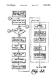
- FIGS. 3, 4 A&B, 5 and 8 A&B constitute a flow chart illustrating the programming of the computer (CPU) to carry out the functions of the system shown in FIG. 1;
- FIG. 6 is a graph showing the adjustment to the current which is sensed (ISI) in the CALC-T2 routine of the program shown in FIGS. 4 and 5;
- FIG. 7 is a curve illustrating the results of the calculation of the duration of the switching pulses which operate the inverter showing the relationship of the duration of these pulses to the inverter current and battery voltage.
- an AC line from the public utility is connected between terminals labelled LINE and NEUT of an SPS system 10.
- the line is connected to a load 12 which may be the power supply of a system which require continuous power, for example a computer system.
- the power supply load 12 may consist of conventional rectifier and filtering and regulating circuits. However, the load may be any load which requires continuous power.
- the line is connected through a switch provided by the contacts of a transfer relay 14. When the relay is not pulled in (energized), the load is connected, as shown, to the output of the SPS system.
- the output of the SPS system is the output of an inverter 16.
- the inverter switches current from a battery 18.
- the high or positive side thereof is shown as VBAT.
- the inverter is controlled and regulated both in the output voltage which it produces and to provide the synchronous relationship between the output voltage and the AC line by a CPU 20.
- the CPU itself may be of the type commercially available, for example, a chip consisting of a Motorola 6805 microprocessor chip with I/O (input/output) ports, a read only memory (ROM) which may be of the erasable type, a random access memory (RAM) and a clock oscillator.
- the I/O ports are shown on the CPU.
- the CPU reads analog voltages through an analog to digital converter (A/D) 22 and provides output drive pulses and levels for operating the inverter and the transfer relay 14.
- the CPU also receives an interrupt (INTR) when the AC line fails (drops below a preset threshold suitably corresponding to 15% of the nominal RMS AC line voltage) which in the United States is 120 VAC RMS at 60 Hz.
- the AC line is connected through a transformer 24 to a diode rectifier and filter circuit 26 which functions as a battery charger for the battery 18.
- the DC voltage from the rectifier 26 is applied to a line failed detector 28 which senses when the nominal voltage drops below a reference typically corresponding to a 15% drop from 120 VAC.
- the line is referred to as failed or in a failed state when it drops below 85% of the nominal 120 VAC RMS value. Otherwise, it is in its unfailed state.
- the voltage from the line is considered insufficient to operate the load 12.
- the detector produces INTR when the AC line enters the failed state.
- the line voltage level is sensed through an isolating diode 30.
- the line voltage frequency and phase is sensed by a zero crossing detector 32.
- the output of the zero crossing detector represents the periodicity of the AC line voltage since it occurs at the zero crossings.
- the zero crossing detector is of conventional design and may be composed of analog or digital circuitry of the type known in the art.
- the output of the zero crossing detector is a pulse train with lagging and leading edges of the pulses thereof at the zero, 180° and 360° points of each cycle of the input AC wave form.
- This output, ZCD is applied to a digital phase detector 34, together with an output FOUT from the CPU 20.
- the frequency of the output of the inverter 16 when the line is in its failed state is constant. When the line has returned, FOUT tracks ZCD.
- the phase detector output is an error signal representing the difference in phase between FOUT and ZCD.
- Other inputs to the CPU via the A/D 22 correspond to the magnitude of the current drawn by the inverter from the battery 18. This current corresponds to the voltage across a current sense resistor 38. Since the currents are relatively high (of the order of 100 Amps) the resistor may be a high power resistor of small value (e.g., 0.0025 Ohms).
- Low pass filters having different time constant(s), Ta-Td provide the input data signals to the CPU 20 via the A/D 22.
- a low pass filter 40 provides the phase difference error signal VCOER.
- Another low pass filter 42 connected to the isolation diode 30 provides the output signal corresponding to the level of the AC line voltage, LVL.
- a low pass filter 46 having a time constant shorter than the duration of several cycles of the AC line voltage provides the instantaneous current output ISI. This current is sampled each time the inverter switches.
- the low pass filter 46 with time constant Td provides the BVL output corresponding to the battery voltage.
- the CPU provides inverter enabling signals Q1D and Q2D.
- the transfer relay is pulled in when the output XFR from the CPU goes high. This output is provided at proper level through a buffer amplifier 50.
- Q3D is enabled during the dwell time between pulses of the train of pulses of opposite polarity which produces the AC output of the inverter.
- the inverter 16 has two field effect transistors Q1 and Q2 which operate the inverter as a push pull inverter to create an AC voltage across the secondary winding 54 of a transformer 56 by alternately switching the battery across different halves of a center tapped primary 58 of the transformer 56.
- Q1 When Q1 is turned on, the battery is connected across one-half of the primary 58 and a positive voltage is applied across the AC output of the inverter (connected to the side of the secondary having the dot to indicate winding sense).
- Q2 When Q2 is turned on, the battery is connected to the other half of the primary 58 and creates a voltage of the opposite polarity across the AC output.
- Q3D is isolated from the inverter circuit by an Opto coupler 62 having an LED 64 and a photo transistor 66.
- a diode bridge circuit 68 is connected across the AC output.
- Q3 clamps the AC output voltage to near zero when Q1 and Q2 are off.
- Q3D is asserted when it is low (although it is shown as a train of positive pulses Q3 drive in FIG. 2 for clarity). Then, the current flows from the battery through the LED 64 and causes FET Q3 to turn on so as to provide essentially a short circuit through the source to drain path of Q3 and a resistor 70 across the bridge 68.
- a network consisting of resistors 72, 74 and 76, capacitors 78, 80 and 82 and diodes 84 and 86 limit the peak source to drain voltage across the field effect transistors Q1 and Q2 and damp switching transients.
- Drive circuits 88 and 90 apply Q1D and Q2D to the gates of Q1 and Q2. These circuits are identical and operate in a similar manner. Only the drive circuit 88 is therefore described in detail.
- a field effect transistor 92 is turned on, which pulls the gate of Q1 to ground through a resistor 94 and a diode 96.
- transistor 92 is off. This turns an NPN transistor 98 on and applies positive voltage to the gate of Q1, turning Q1 on.
- the alternate switching on and off of Q1 and Q2 provide a train of pulses through the primary 58 of the transformer 56. These pulses are translated into a train of successive pulses of opposite polarity in the secondary 54.
- An RC network having a resistor 100 and capacitor 102 is connected across the secondary 54 to damp switching transients caused by the inverter switching actions.
- a varistor 104 is also connected across the secondary 54 (the output of the inverter) to clamp over voltages at the inverter output.
- the timing relationship between the pulse trains produced in the system 10 is shown in FIG. 2. All pulse trains are shown positive for the sake of simplicity.
- the microprocessor of the CPU functions as a variable frequency oscillator or VCO (voltage controlled oscillator) of a phase lock loop in producing FOUT, since FOUT changes in accordance with VCOER.
- VCO voltage controlled oscillator
- FOUT tracks the zero crossings of the AC line voltage.
- the FOUT pulse train has a period equal to 2T1 and consists of half period pulses (duty cycle 50%). In other words, FOUT is high for half a period and low for half a period of each cycle of the AC output voltage.
- the microprocessor 20 While the microprocessor 20 is generating FOUT during inverter operation, it also generates the pulse trains Q1D, Q2D and Q3D (shown in FIG. 2 as Q1DRIVE, Q2DRIVE and Q3DRIVE) to drive the switching transistors Q1 and Q2 and the transistor Q3 which clamps the output to zero during the dwell or dead time of V-OUT.
- the output RMS voltage is proportional to the ratio of T2 to T1 (T2/T1).
- the output frequency is equal to 1/2T1.
- T1 is equal to T2 plus T3.
- the microprocessor controls the output voltage and frequency in response to LVL (the battery voltage level) and the inverter current.
- the instantaneous inverter current ISI is measured shortly after Q1 and Q2 are turned on. If the current is higher than a predetermined value (determined by the ratings of the transistors Q1 and Q2 and other components of the system, inverter operation is stopped by the CPU which turns Q1D and Q2D high effectively connecting the gates of Q1 and Q2 to ground and shutting down inverter operation.
- a predetermined value determined by the ratings of the transistors Q1 and Q2 and other components of the system
- the programming of the CPU is shown in detail in connection with FIGS. 3, 4 and 5. Briefly, there are three modes of operation. First, when the line is in its unfailed state and the line is providing AC power to the load, when the line has failed and is in its failed state and the inverter is supplying AC power to the load, and when the line has returned and the inverter is being synchronized with the AC line so as to enable transfer back to the line when the inverter voltage and line voltage are synchronized with each other.
- the pulse width T2 is increased the duty cycle of the T2 pulse trains Q1D and Q2D is made longer to keep the AC output voltage from the inverter at a constant RMS value while the battery voltage is dropping as the battery discharges.
- T3 is decreased proportionally to keep T1 constant and thus maintain the output AC frequency constant.
- the transfer relay 14 is energized and actually pulls in one cycle of the AC wave form after the expiration of the 8.5 seconds.
- the inverter AC output is phase locked with the AC line wave form so as to enable transient free transfer from the inverter to the AC line.
- the mode of operation where the AC line is in its unfailed state resumes with the CPU acting as a VCO and tracking the AC line wave form producing FOUT in synchronism with the cross overs of the AC line voltage.
- the program in effect when the AC line is present and the inverter is not operating, is shown in FIG. 3.
- T2 and one-half T3 are stored, with different values used for 50 or 60 Hz operation.
- T3/2 is stored since it is desired to switch the inverter switching transistors Q1 and Q2 in the middle of each half cycle which starts at T3/2 after the leading and trailing edges of the FOUT pulses.
- a loop is executed for 200 cycles to initialize the system.
- a timer is loaded with the fixed value of (T1-FX) and started.
- a counter is incremented on each T1 pulse.
- FOUT is toggled. In other words, the bit of the output port which produces FOUT is switched to high if it is low and to low if it is high.
- the initialization loop is exited.
- the next loop in the main program is the AC-Present routine.
- This loop produces FOUT, phase locked with the AC line waveform by operating the microprocessor 20 as a VCO.
- FOUT is toggled.
- a timer is set with a fixed time delay FTD which is less than T1. In the 60 Hz case, this delay may suitably be 7.82 milliseconds (ms).
- the digital signal representing the error voltage VCOER is read.
- a variable time delay TVR is then computed. It has been found that this variable time delay for each half cycle of the AC line wave form is suitably the product of VCOER and 2 (VCOER*2).
- the fixed time delay plus the variable time delay will equal a half cycle, or T1, in duration.
- a timer is set with T3/2.
- the stored initial value is used. It will be appreciated as the description proceeds that the T3/2 value is stored in RAM and is changed as the duty cycle of the AC output pulse train changes. The current value of T3/2 is always used. After the initial interrupt, only the initial value which is stored in the initialization routine is available. This value is used. After the T3/2 timer times out, an interrupt occurs. Now, Q1D is set (low in the circuit illustrated in FIG. 1) to turn Q1 on and Q3 is set (Q3D low in FIG. 1) to turn Q3 off. Now the timer is set with T2. After the first interrupt, the initial value of T2 is used. The timer is started. Sufficient time is now available to execute both the CALC-T2 and the CHK-AC routines.
- the CALC-T2 routine commences by reading ISI and BVL. Then, ISI is adjusted to ISI* which provides a value corresponding to the output voltage corresponding to ISI. This voltage depends upon the nature of the load and the impedances presented by the output transformer 56 and the circuitry associated therewith.
- a table of values relating ISI* to the measured ISI* is stored in ROM. For most resistive loads and for typical power supply loads, the relationship between ISI* and the compensated value ISI corresponding to the output voltage is approximately linear.
- a typical relationship between ISI* in terms of its peak current which is read just after Q1 is turned on, is shown in FIG. 6.
- the BVL is included in the calculation.
- the digital valve corresponding to BVL is acquired with the A/D converter 22 and ISI* is then subtracted from BVL* to create BVL*.
- the computation is by way of subtraction because the increase in current works in an opposite sense in determining the average AC voltage output from the decrease in BVL.
- T2 is calculated based on BVL* which is BVL minus ISI*.
- the calculation carries out a quadratic equation wherein T2 equals a(BVL*) 2 plus b(BVL*) plus c. This equation is plotted in FIG. 7. Since ISI is included in the BVL* (shown as VBAT* in FIG.
- the CHK-AC routine is executed, (see FIG. 4B) as part of the overall inverter routine, to determine when the AC line has returned and to adjust T3 to allow the inverter to phase lock with the input line signal (ZCD), so that the voltage generated by the inverter will be synchronous with the AC line voltage on transfer. Since a relay 14 is energized by XFR and takes time to switch, an impending transfer counter is used. If the count in that counter is equal to zero, the AC line has not been present for 8.5 seconds. It requires three counts, each of which occurs on a toggle of FOUT, to set the XFR FLG.
- the impending transfer counter is equal to zero, transfer is not pending and the AC line voltage level LVL is read. If LVL is within the threshold (+/-15% of the nominal 120 VAC value) the program proceeds to synchronize the inverter output voltage. If, however, LVL is outside of the threshold range, the return counter is set to zero and the inverter routine proceeds via connectors B--B to complete the generation of the QID drive pulse and to generate the Q2D drive pulse, thereby providing the next half cycle of the inverter output wave form.
- FIG. 5 shows this final part of the routine and will be discussed below.
- an ACL (AC line) return counter is incremented.
- the counter is incremented once each half cycle of the output voltage when the line has returned. If the counter has counted up to a predetermined number indicating the the line has returned (is in its unfailed state) for a sufficient time so that it is expected that the line has truly returned (in this case 1020 counts or 510 cycles which is 8.5 seconds at the 60 Hz rate), the CPU generates XFR and causes the relay to pull in, starting switchover from the inverter output to the AC line. The impending transfer counter is then incremented. It will be recalled that when the counter is incremented three times allowing for another cycle of the AC wave form, the transfer flag is set. However, if the predetermined time or 1020 counts of the return counter have not been accumulated, the program continues to a part of the CHK-AC routine which provides for phase locking of the inverter output voltage to the AC line, which has then returned.
- T3 is varied to cause phaselock with the AC line.
- phase difference error voltage, VCOER is then read and these temporary values of T3/2 are adjusted by adding thereto the value of VCOER.
- the adjusted value of T3/2 brings the AC output wave form from the inverter closer into phase lock with the returned AC line. By the time that the 1020 half cycles of the AC line has expired, the inverter output voltage will be in synchronism or substantially in synchronism with the returned AC line. Then, on switchover to the AC line transients and waveform distortion are avoided.
- the dwell or dead time commences by Q1D being turned off and Q3D turned on, both after the timer times out. The timer times out after T2 expires. Then the timer is set with the adjusted or current value of T3/2. After the time out, T3/2 having expired, F-OUT is toggled. This creates the trailing edge of the first F-OUT pulse (see FIG. 2). The timer is again set with T3/2, and when time out occurs the dwell time is completed. Q3D is then turned off and Q2D is turned on to start the pulse which forms the negative half of the cycle.
- the next cycle starts by setting the timer to T2, starting the timer, and while the timer is running executing the CAL-T2 and CHK-AC routines.
- T2 again having expired, the trailing edge of the pulse which provides the negative half of the AC inverter output is formed.
- the dwell time for the last part of the cycle is generated by setting the timer with T3/2.
- F-out is toggled which starts the T1 pulse for the next cycle and completes the first cycle.
- the program then returns via connectors C--C.
- the flow chart is shown that decides where the inverter program (FIGS. 4 & 5) should be entered.
- the entry point depends on where in the AC input voltage waveform the line fail interrup occurred.
- the inverter routine is started at the points indicated by the connectors C-J. By jumping to the appropriate points, the inverter output voltage will commence substantially in phase with the AC line voltage when it failed.
- the line fail detector 28 may be implemented in many different ways.
- One possible way is to pass the output of the rectifier 26 through a low pass filter with a cutoff frequency (3 dB point) of 7 kHz.
- the output of this filter is connected to the inverting input of a comparator and a reference voltage with a DC value equal to 0.21 of the peak of the nominal rectified AC voltage connected to the noninverting input.
- the comparator should have an open collector type of output such that it connects the output to ground or becomes an open circuit. Thus connected, the comparator output will be an open circuit around the zero crossings of the ac line and zero during the peak portions of the ac line.
- An 0.01 uF capacitor is discharged by the comparator through a 365K ohm resistor when the comparator output is zero and charges up through a 191K resistor and a diode connected in series to +5 Volts when the comparator output is an open circuit.
- the voltage across the 0.01 uF capacitor is connected to the inverting input of a second comparator with the noninverting input connected to a dc voltage of 2.5 V.
- the second comparator output will be low when the input AC line voltage falls below 85% of the nominal input ac voltage or 102 V for a 120 V. line.
- the second comparator output may be used as the interrupt signal for the microprocessor to inititate inverter operation.
- the 2.5 Volt input to the second comparator may be varied to change the line dropout threshold level.
Abstract
Description
Claims (39)
Priority Applications (1)
| Application Number | Priority Date | Filing Date | Title |
|---|---|---|---|
| US07/529,066 US5070251A (en) | 1990-05-25 | 1990-05-25 | Computer controlled standby power supply system |
Applications Claiming Priority (1)
| Application Number | Priority Date | Filing Date | Title |
|---|---|---|---|
| US07/529,066 US5070251A (en) | 1990-05-25 | 1990-05-25 | Computer controlled standby power supply system |
Publications (1)
| Publication Number | Publication Date |
|---|---|
| US5070251A true US5070251A (en) | 1991-12-03 |
Family
ID=24108374
Family Applications (1)
| Application Number | Title | Priority Date | Filing Date |
|---|---|---|---|
| US07/529,066 Expired - Lifetime US5070251A (en) | 1990-05-25 | 1990-05-25 | Computer controlled standby power supply system |
Country Status (1)
| Country | Link |
|---|---|
| US (1) | US5070251A (en) |
Cited By (12)
| Publication number | Priority date | Publication date | Assignee | Title |
|---|---|---|---|---|
| US5315533A (en) * | 1991-05-17 | 1994-05-24 | Best Power Technology, Inc. | Back-up uninterruptible power system |
| US5536976A (en) * | 1994-03-03 | 1996-07-16 | Gas Research Institute | Multiple service load solid state switching for controlled cogeneration system |
| US5563776A (en) * | 1994-03-14 | 1996-10-08 | Ecktronics Corp. | Switching-mode, alternating current, wave replication system |
| US5633789A (en) * | 1993-11-24 | 1997-05-27 | Nec Corporation | Failure-free power source device |
| US5640060A (en) * | 1995-02-09 | 1997-06-17 | Basler Electric Company | Apparatus for synchronizing frequency and phase of two voltage sources |
| US5761073A (en) * | 1995-02-09 | 1998-06-02 | Basler Electric Company | Programmable apparatus for synchronizing frequency and phase of two voltage sources |
| US5765001A (en) * | 1996-04-29 | 1998-06-09 | International Business Machines Corporation | Computer system which is operative to change from a normal operating state to a suspend state when a power supply thereof detects that an external source is no longer providing power to said power supply at a predetermined level |
| US5929538A (en) * | 1997-06-27 | 1999-07-27 | Abacus Controls Inc. | Multimode power processor |
| US5995396A (en) * | 1997-12-16 | 1999-11-30 | Lucent Technologies Inc. | Hybrid standby power system, method of operation thereof and telecommunications installation employing the same |
| WO2001063724A1 (en) * | 2000-02-24 | 2001-08-30 | Tatari Mehmet F | Inverterless circuit for an uninterruptible power supply |
| WO2002009058A1 (en) * | 2000-07-21 | 2002-01-31 | Hoffman Gary R | Sensing downed power lines |
| US11368100B2 (en) | 2017-07-13 | 2022-06-21 | Kohler Co. | Generator and battery backup with conversion device |
Citations (26)
| Publication number | Priority date | Publication date | Assignee | Title |
|---|---|---|---|---|
| US3932764A (en) * | 1974-05-15 | 1976-01-13 | Esb Incorporated | Transfer switch and transient eliminator system and method |
| US4259630A (en) * | 1978-11-06 | 1981-03-31 | The United States Of America As Represented By The Secretary Of The Navy | AC Motor controller |
| US4337429A (en) * | 1980-09-04 | 1982-06-29 | The University Of Toledo | A.C. Motor control circuit |
| US4447786A (en) * | 1982-02-12 | 1984-05-08 | Black & Decker Inc. | Waveform synthesizer and motor controller |
| US4466052A (en) * | 1981-12-14 | 1984-08-14 | Thrap Guy C | Programmable DC-TO-AC voltage converter |
| US4466070A (en) * | 1981-04-16 | 1984-08-14 | Siemens Aktiengesellschaft | Control unit with digital addressing memory for a DC-to-AC inverter |
| US4560886A (en) * | 1983-12-22 | 1985-12-24 | Control Technology, Inc. | Alternating current power source |
| US4580064A (en) * | 1982-06-03 | 1986-04-01 | General Electric Company | Method for generating pulse width modulated control signals |
| US4587605A (en) * | 1984-01-19 | 1986-05-06 | Matsushita Electric Industrial Co., Ltd. | Inverter-drive controlling apparatus |
| US4595976A (en) * | 1984-12-27 | 1986-06-17 | Sundstrand Corporation | Inverter control |
| US4608499A (en) * | 1983-02-01 | 1986-08-26 | Silcon Elektronik A/S | Power system and power generation method |
| US4628438A (en) * | 1983-12-16 | 1986-12-09 | Control Concepts Corporation | Power converter apparatus and method employing plural branches |
| US4672228A (en) * | 1985-09-03 | 1987-06-09 | Pioneer Magnetics, Inc. | Battery backup system for switched power supply |
| US4672293A (en) * | 1985-08-26 | 1987-06-09 | Crampton Timothy P | Power-supply/battery back-up power supply/battery charger combination |
| US4675583A (en) * | 1984-12-20 | 1987-06-23 | Siemens Aktiengesellschaft | Circuit arrangement for driving an electronically commutated DC motor |
| US4692145A (en) * | 1984-10-15 | 1987-09-08 | American Hospital Supply Corporation | Power system for infusion pumps |
| US4694194A (en) * | 1985-11-04 | 1987-09-15 | Concurrent Computer Corporation | Power supply with battery backup |
| US4703191A (en) * | 1985-12-09 | 1987-10-27 | Control Technology, Inc. | Reserve power source with power failure detection apparatus |
| US4728808A (en) * | 1985-03-13 | 1988-03-01 | Bet Esh Ran | Uninterruptible power supply system |
| US4779007A (en) * | 1987-02-13 | 1988-10-18 | Unison Technologies, Inc. | Uninterrupted power supply system |
| US4823019A (en) * | 1988-07-21 | 1989-04-18 | Computer Accessories Corporation | Stand-by power system |
| US4827150A (en) * | 1988-06-08 | 1989-05-02 | Reynal Thomas J | Uninterruptible power supply inverter circuit |
| US4876460A (en) * | 1989-03-27 | 1989-10-24 | Intellipower, Inc. | Uninterrupted power supply |
| US4885521A (en) * | 1985-08-26 | 1989-12-05 | Applied Research & Technology, Inc. | Unique computer power system with backup power |
| US4916329A (en) * | 1987-10-05 | 1990-04-10 | Square D Company | Uninterruptible power supply |
| US4954726A (en) * | 1986-07-30 | 1990-09-04 | International Fuel Cells Corporation | Switching an inverter with stored signal sequences |
-
1990
- 1990-05-25 US US07/529,066 patent/US5070251A/en not_active Expired - Lifetime
Patent Citations (26)
| Publication number | Priority date | Publication date | Assignee | Title |
|---|---|---|---|---|
| US3932764A (en) * | 1974-05-15 | 1976-01-13 | Esb Incorporated | Transfer switch and transient eliminator system and method |
| US4259630A (en) * | 1978-11-06 | 1981-03-31 | The United States Of America As Represented By The Secretary Of The Navy | AC Motor controller |
| US4337429A (en) * | 1980-09-04 | 1982-06-29 | The University Of Toledo | A.C. Motor control circuit |
| US4466070A (en) * | 1981-04-16 | 1984-08-14 | Siemens Aktiengesellschaft | Control unit with digital addressing memory for a DC-to-AC inverter |
| US4466052A (en) * | 1981-12-14 | 1984-08-14 | Thrap Guy C | Programmable DC-TO-AC voltage converter |
| US4447786A (en) * | 1982-02-12 | 1984-05-08 | Black & Decker Inc. | Waveform synthesizer and motor controller |
| US4580064A (en) * | 1982-06-03 | 1986-04-01 | General Electric Company | Method for generating pulse width modulated control signals |
| US4608499A (en) * | 1983-02-01 | 1986-08-26 | Silcon Elektronik A/S | Power system and power generation method |
| US4628438A (en) * | 1983-12-16 | 1986-12-09 | Control Concepts Corporation | Power converter apparatus and method employing plural branches |
| US4560886A (en) * | 1983-12-22 | 1985-12-24 | Control Technology, Inc. | Alternating current power source |
| US4587605A (en) * | 1984-01-19 | 1986-05-06 | Matsushita Electric Industrial Co., Ltd. | Inverter-drive controlling apparatus |
| US4692145A (en) * | 1984-10-15 | 1987-09-08 | American Hospital Supply Corporation | Power system for infusion pumps |
| US4675583A (en) * | 1984-12-20 | 1987-06-23 | Siemens Aktiengesellschaft | Circuit arrangement for driving an electronically commutated DC motor |
| US4595976A (en) * | 1984-12-27 | 1986-06-17 | Sundstrand Corporation | Inverter control |
| US4728808A (en) * | 1985-03-13 | 1988-03-01 | Bet Esh Ran | Uninterruptible power supply system |
| US4672293A (en) * | 1985-08-26 | 1987-06-09 | Crampton Timothy P | Power-supply/battery back-up power supply/battery charger combination |
| US4885521A (en) * | 1985-08-26 | 1989-12-05 | Applied Research & Technology, Inc. | Unique computer power system with backup power |
| US4672228A (en) * | 1985-09-03 | 1987-06-09 | Pioneer Magnetics, Inc. | Battery backup system for switched power supply |
| US4694194A (en) * | 1985-11-04 | 1987-09-15 | Concurrent Computer Corporation | Power supply with battery backup |
| US4703191A (en) * | 1985-12-09 | 1987-10-27 | Control Technology, Inc. | Reserve power source with power failure detection apparatus |
| US4954726A (en) * | 1986-07-30 | 1990-09-04 | International Fuel Cells Corporation | Switching an inverter with stored signal sequences |
| US4779007A (en) * | 1987-02-13 | 1988-10-18 | Unison Technologies, Inc. | Uninterrupted power supply system |
| US4916329A (en) * | 1987-10-05 | 1990-04-10 | Square D Company | Uninterruptible power supply |
| US4827150A (en) * | 1988-06-08 | 1989-05-02 | Reynal Thomas J | Uninterruptible power supply inverter circuit |
| US4823019A (en) * | 1988-07-21 | 1989-04-18 | Computer Accessories Corporation | Stand-by power system |
| US4876460A (en) * | 1989-03-27 | 1989-10-24 | Intellipower, Inc. | Uninterrupted power supply |
Non-Patent Citations (1)
| Title |
|---|
| Sola Products Catalog, Catalog 718, pp. 36, 37, 38, 39. * |
Cited By (13)
| Publication number | Priority date | Publication date | Assignee | Title |
|---|---|---|---|---|
| US5315533A (en) * | 1991-05-17 | 1994-05-24 | Best Power Technology, Inc. | Back-up uninterruptible power system |
| US5633789A (en) * | 1993-11-24 | 1997-05-27 | Nec Corporation | Failure-free power source device |
| US5536976A (en) * | 1994-03-03 | 1996-07-16 | Gas Research Institute | Multiple service load solid state switching for controlled cogeneration system |
| US5563776A (en) * | 1994-03-14 | 1996-10-08 | Ecktronics Corp. | Switching-mode, alternating current, wave replication system |
| US5640060A (en) * | 1995-02-09 | 1997-06-17 | Basler Electric Company | Apparatus for synchronizing frequency and phase of two voltage sources |
| US5761073A (en) * | 1995-02-09 | 1998-06-02 | Basler Electric Company | Programmable apparatus for synchronizing frequency and phase of two voltage sources |
| US5765001A (en) * | 1996-04-29 | 1998-06-09 | International Business Machines Corporation | Computer system which is operative to change from a normal operating state to a suspend state when a power supply thereof detects that an external source is no longer providing power to said power supply at a predetermined level |
| US5929538A (en) * | 1997-06-27 | 1999-07-27 | Abacus Controls Inc. | Multimode power processor |
| US5995396A (en) * | 1997-12-16 | 1999-11-30 | Lucent Technologies Inc. | Hybrid standby power system, method of operation thereof and telecommunications installation employing the same |
| WO2001063724A1 (en) * | 2000-02-24 | 2001-08-30 | Tatari Mehmet F | Inverterless circuit for an uninterruptible power supply |
| US6342736B1 (en) * | 2000-02-24 | 2002-01-29 | Rimasoft, L.L.C. | Inverterless circuit for an uninterruptible power supply |
| WO2002009058A1 (en) * | 2000-07-21 | 2002-01-31 | Hoffman Gary R | Sensing downed power lines |
| US11368100B2 (en) | 2017-07-13 | 2022-06-21 | Kohler Co. | Generator and battery backup with conversion device |
Similar Documents
| Publication | Publication Date | Title |
|---|---|---|
| US5670833A (en) | Power transfer method and apparatus for uninterruptible power systems | |
| US5070251A (en) | Computer controlled standby power supply system | |
| US9362781B2 (en) | Uninterruptible power supply system with fast transfer for undervoltage source line failures | |
| US5371666A (en) | Average current mode control apparatus for an AC output amplifier | |
| US5682306A (en) | Switched mode power supply with power factor correction | |
| US5461263A (en) | Method of phase synchronization between two AC signals | |
| US5406468A (en) | Method for minimizing output transient responses in a power supply | |
| US5771161A (en) | Uninterruptable capability for an active power line conditioner | |
| NZ270676A (en) | Modular power supply: battery backup maintains level on high voltage dc bus during ac outages | |
| KR0154818B1 (en) | The controlling system for resonance converter | |
| GB2287843A (en) | Off-Line Uninterruptible Power Supply | |
| US5051683A (en) | Reactive power controller without initial abrupt disturbance on power source | |
| JP2001186767A (en) | Portable generator | |
| JP3922617B2 (en) | Method of correcting output voltage of portable generator | |
| US4122516A (en) | Inverter control apparatus | |
| EP3114752A2 (en) | System and method for uninterruptible power supply intelligent transfer | |
| JPH026306B2 (en) | ||
| JP2002176774A (en) | Voltage regulator | |
| JP2847115B2 (en) | Voltage control method of voltage signal | |
| JPH11341823A (en) | Ac power supply and method of synchronously operating the same | |
| JPS6118405B2 (en) | ||
| JP3057332B2 (en) | Instantaneous interruption power switching method and instantaneous interruption uninterruptible power supply | |
| JPS6114737B2 (en) | ||
| JPS63206165A (en) | Uninterruptible power supply | |
| JP3251769B2 (en) | Restart method of voltage source inverter |
Legal Events
| Date | Code | Title | Description |
|---|---|---|---|
| AS | Assignment |
Owner name: GENERAL SIGNAL CORPORATION, A CORP OF NEW YORK Free format text: ASSIGNMENT OF ASSIGNORS INTEREST.;ASSIGNORS:RHODES, BRUCE R.;BOLLINGER, DAVE;DOMBROWSKI, MARK;REEL/FRAME:005325/0701 Effective date: 19900516 |
|
| STCF | Information on status: patent grant |
Free format text: PATENTED CASE |
|
| FEPP | Fee payment procedure |
Free format text: PAYOR NUMBER ASSIGNED (ORIGINAL EVENT CODE: ASPN); ENTITY STATUS OF PATENT OWNER: LARGE ENTITY |
|
| FPAY | Fee payment |
Year of fee payment: 4 |
|
| FEPP | Fee payment procedure |
Free format text: PAYOR NUMBER ASSIGNED (ORIGINAL EVENT CODE: ASPN); ENTITY STATUS OF PATENT OWNER: LARGE ENTITY |
|
| FPAY | Fee payment |
Year of fee payment: 8 |
|
| AS | Assignment |
Owner name: POWERWARE CORPORATION, A DELAWARE CORPORATION, NOR Free format text: ASSIGNMENT OF ASSIGNORS INTEREST;ASSIGNOR:GENERAL SIGNAL CORPORATION, A DELAWARE CORPORATION;REEL/FRAME:011667/0838 Effective date: 20010130 |
|
| FPAY | Fee payment |
Year of fee payment: 12 |