US5051865A - Multi-layer semiconductor device - Google Patents
Multi-layer semiconductor device Download PDFInfo
- Publication number
- US5051865A US5051865A US07/667,257 US66725791A US5051865A US 5051865 A US5051865 A US 5051865A US 66725791 A US66725791 A US 66725791A US 5051865 A US5051865 A US 5051865A
- Authority
- US
- United States
- Prior art keywords
- heat sink
- semiconductor device
- semiconductor wafers
- plates
- layer
- Prior art date
- Legal status (The legal status is an assumption and is not a legal conclusion. Google has not performed a legal analysis and makes no representation as to the accuracy of the status listed.)
- Expired - Fee Related
Links
Images


Classifications
-
- H—ELECTRICITY
- H01—ELECTRIC ELEMENTS
- H01L—SEMICONDUCTOR DEVICES NOT COVERED BY CLASS H10
- H01L27/00—Devices consisting of a plurality of semiconductor or other solid-state components formed in or on a common substrate
-
- H—ELECTRICITY
- H01—ELECTRIC ELEMENTS
- H01L—SEMICONDUCTOR DEVICES NOT COVERED BY CLASS H10
- H01L23/00—Details of semiconductor or other solid state devices
- H01L23/34—Arrangements for cooling, heating, ventilating or temperature compensation ; Temperature sensing arrangements
- H01L23/36—Selection of materials, or shaping, to facilitate cooling or heating, e.g. heatsinks
-
- H—ELECTRICITY
- H01—ELECTRIC ELEMENTS
- H01L—SEMICONDUCTOR DEVICES NOT COVERED BY CLASS H10
- H01L25/00—Assemblies consisting of a plurality of individual semiconductor or other solid state devices ; Multistep manufacturing processes thereof
- H01L25/03—Assemblies consisting of a plurality of individual semiconductor or other solid state devices ; Multistep manufacturing processes thereof all the devices being of a type provided for in the same subgroup of groups H01L27/00 - H01L33/00, or in a single subclass of H10K, H10N, e.g. assemblies of rectifier diodes
- H01L25/04—Assemblies consisting of a plurality of individual semiconductor or other solid state devices ; Multistep manufacturing processes thereof all the devices being of a type provided for in the same subgroup of groups H01L27/00 - H01L33/00, or in a single subclass of H10K, H10N, e.g. assemblies of rectifier diodes the devices not having separate containers
- H01L25/065—Assemblies consisting of a plurality of individual semiconductor or other solid state devices ; Multistep manufacturing processes thereof all the devices being of a type provided for in the same subgroup of groups H01L27/00 - H01L33/00, or in a single subclass of H10K, H10N, e.g. assemblies of rectifier diodes the devices not having separate containers the devices being of a type provided for in group H01L27/00
- H01L25/0657—Stacked arrangements of devices
-
- H—ELECTRICITY
- H01—ELECTRIC ELEMENTS
- H01L—SEMICONDUCTOR DEVICES NOT COVERED BY CLASS H10
- H01L2224/00—Indexing scheme for arrangements for connecting or disconnecting semiconductor or solid-state bodies and methods related thereto as covered by H01L24/00
- H01L2224/01—Means for bonding being attached to, or being formed on, the surface to be connected, e.g. chip-to-package, die-attach, "first-level" interconnects; Manufacturing methods related thereto
- H01L2224/42—Wire connectors; Manufacturing methods related thereto
- H01L2224/44—Structure, shape, material or disposition of the wire connectors prior to the connecting process
- H01L2224/45—Structure, shape, material or disposition of the wire connectors prior to the connecting process of an individual wire connector
- H01L2224/45001—Core members of the connector
- H01L2224/45099—Material
- H01L2224/451—Material with a principal constituent of the material being a metal or a metalloid, e.g. boron (B), silicon (Si), germanium (Ge), arsenic (As), antimony (Sb), tellurium (Te) and polonium (Po), and alloys thereof
- H01L2224/45117—Material with a principal constituent of the material being a metal or a metalloid, e.g. boron (B), silicon (Si), germanium (Ge), arsenic (As), antimony (Sb), tellurium (Te) and polonium (Po), and alloys thereof the principal constituent melting at a temperature of greater than or equal to 400°C and less than 950°C
- H01L2224/45124—Aluminium (Al) as principal constituent
-
- H—ELECTRICITY
- H01—ELECTRIC ELEMENTS
- H01L—SEMICONDUCTOR DEVICES NOT COVERED BY CLASS H10
- H01L2224/00—Indexing scheme for arrangements for connecting or disconnecting semiconductor or solid-state bodies and methods related thereto as covered by H01L24/00
- H01L2224/01—Means for bonding being attached to, or being formed on, the surface to be connected, e.g. chip-to-package, die-attach, "first-level" interconnects; Manufacturing methods related thereto
- H01L2224/42—Wire connectors; Manufacturing methods related thereto
- H01L2224/47—Structure, shape, material or disposition of the wire connectors after the connecting process
- H01L2224/48—Structure, shape, material or disposition of the wire connectors after the connecting process of an individual wire connector
- H01L2224/4805—Shape
- H01L2224/4809—Loop shape
- H01L2224/48091—Arched
-
- H—ELECTRICITY
- H01—ELECTRIC ELEMENTS
- H01L—SEMICONDUCTOR DEVICES NOT COVERED BY CLASS H10
- H01L2224/00—Indexing scheme for arrangements for connecting or disconnecting semiconductor or solid-state bodies and methods related thereto as covered by H01L24/00
- H01L2224/01—Means for bonding being attached to, or being formed on, the surface to be connected, e.g. chip-to-package, die-attach, "first-level" interconnects; Manufacturing methods related thereto
- H01L2224/42—Wire connectors; Manufacturing methods related thereto
- H01L2224/47—Structure, shape, material or disposition of the wire connectors after the connecting process
- H01L2224/48—Structure, shape, material or disposition of the wire connectors after the connecting process of an individual wire connector
- H01L2224/481—Disposition
- H01L2224/48151—Connecting between a semiconductor or solid-state body and an item not being a semiconductor or solid-state body, e.g. chip-to-substrate, chip-to-passive
- H01L2224/48221—Connecting between a semiconductor or solid-state body and an item not being a semiconductor or solid-state body, e.g. chip-to-substrate, chip-to-passive the body and the item being stacked
- H01L2224/48225—Connecting between a semiconductor or solid-state body and an item not being a semiconductor or solid-state body, e.g. chip-to-substrate, chip-to-passive the body and the item being stacked the item being non-metallic, e.g. insulating substrate with or without metallisation
- H01L2224/48227—Connecting between a semiconductor or solid-state body and an item not being a semiconductor or solid-state body, e.g. chip-to-substrate, chip-to-passive the body and the item being stacked the item being non-metallic, e.g. insulating substrate with or without metallisation connecting the wire to a bond pad of the item
-
- H—ELECTRICITY
- H01—ELECTRIC ELEMENTS
- H01L—SEMICONDUCTOR DEVICES NOT COVERED BY CLASS H10
- H01L2224/00—Indexing scheme for arrangements for connecting or disconnecting semiconductor or solid-state bodies and methods related thereto as covered by H01L24/00
- H01L2224/01—Means for bonding being attached to, or being formed on, the surface to be connected, e.g. chip-to-package, die-attach, "first-level" interconnects; Manufacturing methods related thereto
- H01L2224/42—Wire connectors; Manufacturing methods related thereto
- H01L2224/47—Structure, shape, material or disposition of the wire connectors after the connecting process
- H01L2224/49—Structure, shape, material or disposition of the wire connectors after the connecting process of a plurality of wire connectors
- H01L2224/491—Disposition
- H01L2224/4912—Layout
- H01L2224/49171—Fan-out arrangements
-
- H—ELECTRICITY
- H01—ELECTRIC ELEMENTS
- H01L—SEMICONDUCTOR DEVICES NOT COVERED BY CLASS H10
- H01L2225/00—Details relating to assemblies covered by the group H01L25/00 but not provided for in its subgroups
- H01L2225/03—All the devices being of a type provided for in the same subgroup of groups H01L27/00 - H01L33/648 and H10K99/00
- H01L2225/04—All the devices being of a type provided for in the same subgroup of groups H01L27/00 - H01L33/648 and H10K99/00 the devices not having separate containers
- H01L2225/065—All the devices being of a type provided for in the same subgroup of groups H01L27/00 - H01L33/648 and H10K99/00 the devices not having separate containers the devices being of a type provided for in group H01L27/00
- H01L2225/06503—Stacked arrangements of devices
- H01L2225/0651—Wire or wire-like electrical connections from device to substrate
-
- H—ELECTRICITY
- H01—ELECTRIC ELEMENTS
- H01L—SEMICONDUCTOR DEVICES NOT COVERED BY CLASS H10
- H01L2225/00—Details relating to assemblies covered by the group H01L25/00 but not provided for in its subgroups
- H01L2225/03—All the devices being of a type provided for in the same subgroup of groups H01L27/00 - H01L33/648 and H10K99/00
- H01L2225/04—All the devices being of a type provided for in the same subgroup of groups H01L27/00 - H01L33/648 and H10K99/00 the devices not having separate containers
- H01L2225/065—All the devices being of a type provided for in the same subgroup of groups H01L27/00 - H01L33/648 and H10K99/00 the devices not having separate containers the devices being of a type provided for in group H01L27/00
- H01L2225/06503—Stacked arrangements of devices
- H01L2225/06527—Special adaptation of electrical connections, e.g. rewiring, engineering changes, pressure contacts, layout
-
- H—ELECTRICITY
- H01—ELECTRIC ELEMENTS
- H01L—SEMICONDUCTOR DEVICES NOT COVERED BY CLASS H10
- H01L2225/00—Details relating to assemblies covered by the group H01L25/00 but not provided for in its subgroups
- H01L2225/03—All the devices being of a type provided for in the same subgroup of groups H01L27/00 - H01L33/648 and H10K99/00
- H01L2225/04—All the devices being of a type provided for in the same subgroup of groups H01L27/00 - H01L33/648 and H10K99/00 the devices not having separate containers
- H01L2225/065—All the devices being of a type provided for in the same subgroup of groups H01L27/00 - H01L33/648 and H10K99/00 the devices not having separate containers the devices being of a type provided for in group H01L27/00
- H01L2225/06503—Stacked arrangements of devices
- H01L2225/06551—Conductive connections on the side of the device
-
- H—ELECTRICITY
- H01—ELECTRIC ELEMENTS
- H01L—SEMICONDUCTOR DEVICES NOT COVERED BY CLASS H10
- H01L2225/00—Details relating to assemblies covered by the group H01L25/00 but not provided for in its subgroups
- H01L2225/03—All the devices being of a type provided for in the same subgroup of groups H01L27/00 - H01L33/648 and H10K99/00
- H01L2225/04—All the devices being of a type provided for in the same subgroup of groups H01L27/00 - H01L33/648 and H10K99/00 the devices not having separate containers
- H01L2225/065—All the devices being of a type provided for in the same subgroup of groups H01L27/00 - H01L33/648 and H10K99/00 the devices not having separate containers the devices being of a type provided for in group H01L27/00
- H01L2225/06503—Stacked arrangements of devices
- H01L2225/06555—Geometry of the stack, e.g. form of the devices, geometry to facilitate stacking
-
- H—ELECTRICITY
- H01—ELECTRIC ELEMENTS
- H01L—SEMICONDUCTOR DEVICES NOT COVERED BY CLASS H10
- H01L2225/00—Details relating to assemblies covered by the group H01L25/00 but not provided for in its subgroups
- H01L2225/03—All the devices being of a type provided for in the same subgroup of groups H01L27/00 - H01L33/648 and H10K99/00
- H01L2225/04—All the devices being of a type provided for in the same subgroup of groups H01L27/00 - H01L33/648 and H10K99/00 the devices not having separate containers
- H01L2225/065—All the devices being of a type provided for in the same subgroup of groups H01L27/00 - H01L33/648 and H10K99/00 the devices not having separate containers the devices being of a type provided for in group H01L27/00
- H01L2225/06503—Stacked arrangements of devices
- H01L2225/06589—Thermal management, e.g. cooling
-
- H—ELECTRICITY
- H01—ELECTRIC ELEMENTS
- H01L—SEMICONDUCTOR DEVICES NOT COVERED BY CLASS H10
- H01L24/00—Arrangements for connecting or disconnecting semiconductor or solid-state bodies; Methods or apparatus related thereto
- H01L24/01—Means for bonding being attached to, or being formed on, the surface to be connected, e.g. chip-to-package, die-attach, "first-level" interconnects; Manufacturing methods related thereto
- H01L24/42—Wire connectors; Manufacturing methods related thereto
- H01L24/44—Structure, shape, material or disposition of the wire connectors prior to the connecting process
- H01L24/45—Structure, shape, material or disposition of the wire connectors prior to the connecting process of an individual wire connector
-
- H—ELECTRICITY
- H01—ELECTRIC ELEMENTS
- H01L—SEMICONDUCTOR DEVICES NOT COVERED BY CLASS H10
- H01L24/00—Arrangements for connecting or disconnecting semiconductor or solid-state bodies; Methods or apparatus related thereto
- H01L24/01—Means for bonding being attached to, or being formed on, the surface to be connected, e.g. chip-to-package, die-attach, "first-level" interconnects; Manufacturing methods related thereto
- H01L24/42—Wire connectors; Manufacturing methods related thereto
- H01L24/47—Structure, shape, material or disposition of the wire connectors after the connecting process
- H01L24/48—Structure, shape, material or disposition of the wire connectors after the connecting process of an individual wire connector
-
- H—ELECTRICITY
- H01—ELECTRIC ELEMENTS
- H01L—SEMICONDUCTOR DEVICES NOT COVERED BY CLASS H10
- H01L24/00—Arrangements for connecting or disconnecting semiconductor or solid-state bodies; Methods or apparatus related thereto
- H01L24/01—Means for bonding being attached to, or being formed on, the surface to be connected, e.g. chip-to-package, die-attach, "first-level" interconnects; Manufacturing methods related thereto
- H01L24/42—Wire connectors; Manufacturing methods related thereto
- H01L24/47—Structure, shape, material or disposition of the wire connectors after the connecting process
- H01L24/49—Structure, shape, material or disposition of the wire connectors after the connecting process of a plurality of wire connectors
-
- H—ELECTRICITY
- H01—ELECTRIC ELEMENTS
- H01L—SEMICONDUCTOR DEVICES NOT COVERED BY CLASS H10
- H01L2924/00—Indexing scheme for arrangements or methods for connecting or disconnecting semiconductor or solid-state bodies as covered by H01L24/00
- H01L2924/01—Chemical elements
- H01L2924/01019—Potassium [K]
-
- H—ELECTRICITY
- H01—ELECTRIC ELEMENTS
- H01L—SEMICONDUCTOR DEVICES NOT COVERED BY CLASS H10
- H01L2924/00—Indexing scheme for arrangements or methods for connecting or disconnecting semiconductor or solid-state bodies as covered by H01L24/00
- H01L2924/10—Details of semiconductor or other solid state devices to be connected
- H01L2924/102—Material of the semiconductor or solid state bodies
- H01L2924/1025—Semiconducting materials
- H01L2924/10251—Elemental semiconductors, i.e. Group IV
- H01L2924/10253—Silicon [Si]
-
- H—ELECTRICITY
- H01—ELECTRIC ELEMENTS
- H01L—SEMICONDUCTOR DEVICES NOT COVERED BY CLASS H10
- H01L2924/00—Indexing scheme for arrangements or methods for connecting or disconnecting semiconductor or solid-state bodies as covered by H01L24/00
- H01L2924/10—Details of semiconductor or other solid state devices to be connected
- H01L2924/11—Device type
- H01L2924/12—Passive devices, e.g. 2 terminal devices
- H01L2924/1204—Optical Diode
- H01L2924/12042—LASER
-
- H—ELECTRICITY
- H01—ELECTRIC ELEMENTS
- H01L—SEMICONDUCTOR DEVICES NOT COVERED BY CLASS H10
- H01L2924/00—Indexing scheme for arrangements or methods for connecting or disconnecting semiconductor or solid-state bodies as covered by H01L24/00
- H01L2924/10—Details of semiconductor or other solid state devices to be connected
- H01L2924/11—Device type
- H01L2924/13—Discrete devices, e.g. 3 terminal devices
- H01L2924/1304—Transistor
- H01L2924/1306—Field-effect transistor [FET]
- H01L2924/13091—Metal-Oxide-Semiconductor Field-Effect Transistor [MOSFET]
-
- H—ELECTRICITY
- H01—ELECTRIC ELEMENTS
- H01L—SEMICONDUCTOR DEVICES NOT COVERED BY CLASS H10
- H01L2924/00—Indexing scheme for arrangements or methods for connecting or disconnecting semiconductor or solid-state bodies as covered by H01L24/00
- H01L2924/10—Details of semiconductor or other solid state devices to be connected
- H01L2924/11—Device type
- H01L2924/14—Integrated circuits
-
- H—ELECTRICITY
- H01—ELECTRIC ELEMENTS
- H01L—SEMICONDUCTOR DEVICES NOT COVERED BY CLASS H10
- H01L2924/00—Indexing scheme for arrangements or methods for connecting or disconnecting semiconductor or solid-state bodies as covered by H01L24/00
- H01L2924/15—Details of package parts other than the semiconductor or other solid state devices to be connected
- H01L2924/151—Die mounting substrate
- H01L2924/1515—Shape
- H01L2924/15153—Shape the die mounting substrate comprising a recess for hosting the device
Definitions
- the present invention relates to a multi-layer semiconductor device, more particularly, it relates to a multi-layer semiconductor device having a heat sink.
- a multi-layer semiconductor device comprising: a stacked wafer body consisting of a plurality of sets of two semiconductor wafers and heat sink plates interposed therebetween, an end of the heat sink plate for each set of wafers being exposed at at least one of the side surfaces of the stacked wafer body.
- An intermediate connecting circuit is provided for connecting circuits in each of the sets of wafers.
- the intermediate connecting circuit is provided on at least one side surface other than the surface at which the ends of the heat sink plates are exposed.
- FIG. 1 is a cross-sectional view of a prior multi-layer semiconductor device
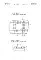
- FIG. 2A is a view of conventional IC chips
- FIG. 2B is a cross-sectional view of FIG. 2A;
- FIG. 3 is a side view of a device according to the present invention.
- FIG. 4 is a view of IC chips in a silicon wafer
- FIG. 5 is an enlarged view of a portion A of FIG. 4;
- FIG. 6 is a schematic cross-sectional view taken along a slice line of FIG. 5;
- FIGS. 7 to 9 and FIG. 11 are views explaining a method for producing a stacked structure as a base unit structure
- FIG. 10A is a view of an example for explaining thermal resistance
- FIG. 10B is a thermal equivalent circuit diagram of FIG. 10A
- FIG. 12 is a view of a slice B in FIG. 11;
- FIG. 13 is an enlarged view of a sliced portion of FIG. 12;
- FIG. 14 is a cross-sectional view taken along a line C--C of FIG. 13;
- FIG. 15 is an enlarged view of a portion D of FIG. 13;
- FIGS. 16 and 17 are perspective views of an example of the present invention having a heat sink with grooves and fins;
- FIG. 18 is a view of another example of the present invention.
- FIG. 1 shows a cross-sectional view of a prior multi-layer semiconductor device which the present inventor proposed before.
- a set 4 of integrated circuits consisting of semiconductor wafers 1 facing each other through a metal plate 3 are stacked in three layers.
- a plurality of semiconductor elements 2 and wirings are formed to constitute a plurality of integrated circuits.
- electrode wirings 13 are formed between circuits included in respective layers of the semiconductor device chips. In such astructure of the multi-layer semiconductor device, the height thereof is remarkably reduced, and the integrated density of the device can be accordingly improved.
- FIG. 2A shows many similar IC chips 11 formed on a wafer, wherein the IC chips 11 have been separated from each other by cutting the slice line 16 of the wafer, and as also shown in FIG. 2A, an IC element forming the region 12 is connected to pad electrodes 15 through aluminum wiring 14.
- the electrodes 15 are formed by wire bonding to the pad electrodes 15.
- FIG. 2B shows a cross-sectional view of FIG. 2A.
- 19 and 20 denote a lead-frame and ceramic, respectively.
- FIG. 3 shows a side view of a device according to the present invention.
- FIG. 3 shows a wafer set 4 of two silicon wafers 1 and a heat sink plate 3 interposed therebetween.
- the heat sink plate is made of, for example, aluminum and copper.
- the sets 4 are stacked in a wafer stacked body 6, and the ends of the heat sink plate 3 are exposed.
- Intermediate connecting circuits connecting and controlling the semiconductor elements 2 are provided on a surface of a multi-layer semiconductor IC chip 7.
- Transistors, capacitors, resistance, etc., are formed on a polished side surface of a semiconductor wafer together with wirings.
- the semiconductor wafers 1 are connected through an insulating layer 5.
- semiconductor elements are formed on a (100) surface of a silicon wafer 1, and IC chips is 11 (only one chip shown) are formed on asuitable position so that side surface circuits can be formed together in apost process.
- the lines 16 denote the slice lines.
- Alignmentmarks 22 are provided on the IC chip 11.
- FIG. 5 is an enlarged view of a portion A of FIG. 4.
- the electrical connections between the stacked IC chips in the present invention are carried out on a side surface of an IC chip.
- the output electrodes drawn from the integrated elements are embedded in a slice surface.
- Aluminum lead wiring is formed at the same time as the aluminum wiring is finally formed during the formation of the integrated semiconductor element region 12.
- the aluminum lead wiring is connected to the embedded electrodes 24 formed along the slice lines 16.
- This aluminum wiring 25 is formed by a process wherein a 1 ⁇ m thick aluminum layer is formed by a sputtering process and patterned.
- the embedded electrodes 24 are 20 ⁇ m in width and 100 ⁇ m in length. After the formation of the electrode, a usual passivationfilm is formed.
- FIG. 6 is a schematic cross-sectional view taken along a slice line of FIG.5. As shown in FIG. 6 on the output electrodes 24, a passivation layer 26 is provided. A method for producing a base unit structure including an aluminum plate and silicon wafers connected through the aluminum plate will now be described.
- an IC side surface of a silicon wafer 1 is adhered to asupporting quartz plate 30a by a thermoplastic resin 31 such as picene.
- a back, non-adhered surface of the silicon wafer 1 is polished for reducing thickness to a total thickness of 200 ⁇ m.
- the supporting quartz plate 30a is aligned with the silicon wafer by an alignment mark 22. Another is formed, and, as shown in FIG. 8, the two structures are permanently bonded to an aluminum plate 3 having a thickness of, for example, 0.05 to 1 mm, by silver paste or Au-Sn solder 33.
- thermoplastic resin is heated and melted and the quartz plates 30a on both sides are separated from the silicon wafers 1 so that a base unit structure including a heat sink aluminum plate 3 and silicon wafers 33 is formed.
- the base unit structure is cleaned by trichlene.
- one base unit structure is connected to another base unit structure by a silicone resin.
- One of the base unit structures is fixed to a quartz plate 30b by vacuum chucking, and the other base unit structure is permanently bonded to a ceramic substrate 40 by a silicone resin such as PLOS (polyladder organosiloxane).
- PLOS polyladder organosiloxane
- the IC chip can be cooled enough by an aluminum plate having a thickness of 70 ⁇ m.
- the thickness of the cooling metal plate can be calculated.
- the thermal resistance is described by a following expression: ##EQU1##R: thermal resistance of the metal plate, K: thermal conductivity of the metal plate,
- FIG. 10A is an example for explaining thermal resistance and FIG. 10B is anequivalence thermal circuit diagram of FIG. 10A.
- R c , R e and R sink are a contact thermal resistance between an IC chip and a metal plate, an average thermal resistance of a metal plate and contact thermal resistance with a heat sink, respectively.
- the total thermal resistance R is substantially shown as R e .
- maximum heat capacity is 10 W.
- the thickness (d) of the aluminum and copper cooling plates are 0.07 and 0.042 cm, respectively.
- an aluminum plate having a thickness of 0.5 mm is used. Consequently, the total thickness of the two IC chips and the aluminum plate is about 1 mm. Since a 20 ⁇ 20 mm chip is formed on the 6 inch silicon wafer, it is better that twenty base unit structures are stacked to form a three-dimensional IC cubic unit. Furthermore, to increase efficiency of the formation of the side surface wiring, it is best that one hundred basic units forming five layers of three-dimentional IC cubic units are stacked, whereby the production efficiency of the side surface wiring is increased five-fold. The width of the side surface of only 20 basic units is 20 mm. On the other hand, since a size of a mask to form side surface circuits is 150 mm or more five layers of the IC cubic unit must be formed so as not to make useless space.
- the stacked structure is shown in FIG. 11.
- a slice B shown in FIG. 12 and FIG. 11 is obtained.
- the sliced surfaces should be polished to a mirror surface inwhich an embedded electrode has been previously exposed.
- IC cubic units of the same number of IC chips formed on a wafer can be produced.
- FIG. 11 five set of 20 layers of the basic unit structure are stacked.
- the feature of the present invention resides in that after stacking a lot of the IC cubic units, slices are produced and side surfacecircuits can be collectively formed using one mask by well known process. As shown in FIG. 12, the heat sink side is the back side of the wiring side.
- FIG. 13 shows an enlarged view of a polished wiring side portion of FIG. 12, and FIG. 14 shows a cross-sectional view thereof taken along a line C--C of FIG. 13.
- the aluminum plates 3, silicon wafers 1, device formation layer3a, adhesive 33 and embedded electrodes 24 are exposed.
- a 5000 ⁇ thick SiO 2 layer 43 is first formed on the entire silicon wafer by a well known chemical vapour deposition (CVD) process. Then, after, for example, Si0 2 of a transistor formation region is removed, a gate oxide film is formed by laser oxidation, a tungstensilicide gate metal is formed, and a source anda drain are formed by ion-implanting and laser annealing processes, so that a MOS transistor is formed.
- CVD chemical vapour deposition
- FIG. 15 is an enlarged view of the portion D in FIG. 13.
- 41 and 25 denote an aluminum bonding pad and an aluminum wiring, respectively.
- the silicone resin adhesive layer is etched by oxygen plasma and a silicon substrate is etched selectively by a mixed etchant including HClO 4 and H 3 PO 4 , so that an aluminum plate having an end extended for 1 ⁇ m can be obtained.
- a mixed etchant including HClO 4 and H 3 PO 4
- the etching is simultaneously carried out in all IC cubic units included inthe slice of FIG. 11.
- a slice shown in FIG. 12 is further cut to a three-dimensional IC cubic unit (20 ⁇ 20 ⁇ 20 mm), a surface other than a heat sink surface is covered by a polyimide, and a pad aluminum electrode is opened so that a structure shown in FIG. 16 is obtained.
- 52 is an aluminum heat sink having dissipating fins.
- Grooves to be fixed to the extended aluminum plate by solder 49 are provided on a surface of the aluminum heat sink 52.
- FIG. 17 shows a structure of a three-dimensional IC package according to the example of the present invention.
- FIG. 18 shows another example of the present invention.
- FIG. 18 a structure having a flat heat sink side surface wherein a multi-layer semiconductor IC chip 7 is formed and adhered to a large heat sink plate 50 with solder.
- an intermediate connecting circuit 9 is provided on a surface of the structure. Accordingly, as aluminum plates for dissipation are connected to the largeheat sink plate, the heat sink effects during operation are improved.
Landscapes
- Engineering & Computer Science (AREA)
- Power Engineering (AREA)
- Microelectronics & Electronic Packaging (AREA)
- Physics & Mathematics (AREA)
- Condensed Matter Physics & Semiconductors (AREA)
- General Physics & Mathematics (AREA)
- Computer Hardware Design (AREA)
- Chemical & Material Sciences (AREA)
- Materials Engineering (AREA)
- Cooling Or The Like Of Semiconductors Or Solid State Devices (AREA)
- Container, Conveyance, Adherence, Positioning, Of Wafer (AREA)
Abstract
A multi-layer semiconductor device which includes a stacked wafer body having a plurality of sets of two semiconductor wafers and a heat sink plate interposed therebetween. An end of the heat sink plate of each set of wafers is exposed at at least one of the side surfaces of the stacked wafer body.
An intermediate connecting circuit is provided for connecting circuits in each of the sets of two semiconductors wafers, the intermediate connecting circuit is provided on at least one side surface other than the surface at which the ends of the heat sink plate are exposed.
Description
This application is a continuation of application Ser. No. 07,443,070, filed Nov. 30, 1989, which is a continuation of Ser. No. 222,341, filed July 20, 1988, and which is a continuation of Ser. No. 874,852, filed June 16, 1986 now abandoned.
1. Field of the Invention
The present invention relates to a multi-layer semiconductor device, more particularly, it relates to a multi-layer semiconductor device having a heat sink.
2. Description of the Related Art
To improve the integration density of an integrated circuit, consideration has been given to the use of a planar integration density and a packaging technique therefor. Particularly, to improve the integration density, a mutualization of patterns has been carried out.
However, these considerations are self-evidently limited from the viewpoint of miniaturization of the integrated circuit.
Under this background, the present inventor filed Japanese Patent Application No. 59-60943, wherein integrated circuit chips are stacked to produce a stacked chip type multi-layer semiconductor device. The height of this structure of the multi-layer semiconductor device is decreased, and thus the integrated density is improved.
In such a structure of the multi-layer semiconductor device, however, the exotherm per unit volume is increased, which results in overheating, and thus it is relatively easy for a power-transistor having a high electrical heat element to be formed in the structure.
Moreover, since a heat sink metal plate is provided between stacked IC chips, electrical interconnection between each IC chip using a bump is difficult.
It is an object of the present invention to provide a multi-layer semiconductor device having an improved heat dissipation efficiency.
Therefore, according to the present invention, there is provided a multi-layer semiconductor device comprising: a stacked wafer body consisting of a plurality of sets of two semiconductor wafers and heat sink plates interposed therebetween, an end of the heat sink plate for each set of wafers being exposed at at least one of the side surfaces of the stacked wafer body.
An intermediate connecting circuit is provided for connecting circuits in each of the sets of wafers. The intermediate connecting circuit is provided on at least one side surface other than the surface at which the ends of the heat sink plates are exposed.
FIG. 1 is a cross-sectional view of a prior multi-layer semiconductor device;
FIG. 2A is a view of conventional IC chips;
FIG. 2B is a cross-sectional view of FIG. 2A;
FIG. 3 is a side view of a device according to the present invention;
FIG. 4 is a view of IC chips in a silicon wafer;
FIG. 5 is an enlarged view of a portion A of FIG. 4;
FIG. 6 is a schematic cross-sectional view taken along a slice line of FIG. 5;
FIGS. 7 to 9 and FIG. 11 are views explaining a method for producing a stacked structure as a base unit structure;
FIG. 10A is a view of an example for explaining thermal resistance;
FIG. 10B is a thermal equivalent circuit diagram of FIG. 10A;
FIG. 12 is a view of a slice B in FIG. 11;
FIG. 13 is an enlarged view of a sliced portion of FIG. 12;
FIG. 14 is a cross-sectional view taken along a line C--C of FIG. 13;
FIG. 15 is an enlarged view of a portion D of FIG. 13;
FIGS. 16 and 17 are perspective views of an example of the present invention having a heat sink with grooves and fins; and,
FIG. 18 is a view of another example of the present invention.
Before describing the preferred embodiments of the present invention, an explanation will be given of the related art.
FIG. 1 shows a cross-sectional view of a prior multi-layer semiconductor device which the present inventor proposed before. As shown in FIG. 1, a set 4 of integrated circuits consisting of semiconductor wafers 1 facing each other through a metal plate 3 are stacked in three layers. On the semiconductor wafer 1, a plurality of semiconductor elements 2 and wiringsare formed to constitute a plurality of integrated circuits. In the stacked-wafer structure 6, in which sets of multi-layer integrated circuits are formed, electrode wirings 13 are formed between circuits included in respective layers of the semiconductor device chips. In such astructure of the multi-layer semiconductor device, the height thereof is remarkably reduced, and the integrated density of the device can be accordingly improved.
But, when the semiconductor chips are formed, the exotherm per unit volume is increased during the operation thereof, and a problem of overheating occurs. Further, since only wiring was formed on a side surface, additional circuits for controlling electric signals between IC chips of each semiconductor device must be formed in inside respective IC chips or additional IC chips consist only of controlling circuits. Thus response ofa three dimensional signal is delayed. Additionally, the efficiency of the wiring process on a side surface is greatly decreased.
FIG. 2A shows many similar IC chips 11 formed on a wafer, wherein the IC chips 11 have been separated from each other by cutting the slice line 16 of the wafer, and as also shown in FIG. 2A, an IC element forming the region 12 is connected to pad electrodes 15 through aluminum wiring 14.
The electrodes 15 are formed by wire bonding to the pad electrodes 15.
FIG. 2B shows a cross-sectional view of FIG. 2A. In FIG. 2B, 19 and 20 denote a lead-frame and ceramic, respectively.
FIG. 3 shows a side view of a device according to the present invention.
FIG. 3 shows a wafer set 4 of two silicon wafers 1 and a heat sink plate 3 interposed therebetween. The heat sink plate is made of, for example, aluminum and copper.
The sets 4 are stacked in a wafer stacked body 6, and the ends of the heat sink plate 3 are exposed.
Intermediate connecting circuits connecting and controlling the semiconductor elements 2 are provided on a surface of a multi-layer semiconductor IC chip 7. Transistors, capacitors, resistance, etc., are formed on a polished side surface of a semiconductor wafer together with wirings. The semiconductor wafers 1 are connected through an insulating layer 5.
A method for producing a structure of the present invention will now be explained.
As shown in FIG. 4, semiconductor elements are formed on a (100) surface ofa silicon wafer 1, and IC chips is 11 (only one chip shown) are formed on asuitable position so that side surface circuits can be formed together in apost process. In the figure, the lines 16 denote the slice lines. Alignmentmarks 22 are provided on the IC chip 11.
FIG. 5 is an enlarged view of a portion A of FIG. 4.
The electrical connections between the stacked IC chips in the present invention are carried out on a side surface of an IC chip. Thus, as shown in FIG. 5 the output electrodes drawn from the integrated elements are embedded in a slice surface.
Aluminum lead wiring is formed at the same time as the aluminum wiring is finally formed during the formation of the integrated semiconductor element region 12.
The aluminum lead wiring is connected to the embedded electrodes 24 formed along the slice lines 16. This aluminum wiring 25 is formed by a process wherein a 1 μm thick aluminum layer is formed by a sputtering process and patterned. The embedded electrodes 24 are 20 μm in width and 100 μm in length. After the formation of the electrode, a usual passivationfilm is formed.
FIG. 6 is a schematic cross-sectional view taken along a slice line of FIG.5. As shown in FIG. 6 on the output electrodes 24, a passivation layer 26 is provided. A method for producing a base unit structure including an aluminum plate and silicon wafers connected through the aluminum plate will now be described.
As shown in FIG. 7, an IC side surface of a silicon wafer 1 is adhered to asupporting quartz plate 30a by a thermoplastic resin 31 such as picene. A back, non-adhered surface of the silicon wafer 1 is polished for reducing thickness to a total thickness of 200 μm.
The supporting quartz plate 30a is aligned with the silicon wafer by an alignment mark 22. Another is formed, and, as shown in FIG. 8, the two structures are permanently bonded to an aluminum plate 3 having a thickness of, for example, 0.05 to 1 mm, by silver paste or Au-Sn solder 33.
Then, the thermoplastic resin is heated and melted and the quartz plates 30a on both sides are separated from the silicon wafers 1 so that a base unit structure including a heat sink aluminum plate 3 and silicon wafers 33 is formed.
After formation, the base unit structure is cleaned by trichlene.
Then, one base unit structure is connected to another base unit structure by a silicone resin. One of the base unit structures is fixed to a quartz plate 30b by vacuum chucking, and the other base unit structure is permanently bonded to a ceramic substrate 40 by a silicone resin such as PLOS (polyladder organosiloxane). Thus, the base unit structures are stacked as shown in FIG. 9.
When the consumption of electric power per one IC chip is assumed to be 0.5watt, the IC chip can be cooled enough by an aluminum plate having a thickness of 70 μm.
The thickness of the cooling metal plate can be calculated. In cooling the metal plate the thermal resistance is described by a following expression: ##EQU1##R: thermal resistance of the metal plate, K: thermal conductivity of the metal plate,
l: length of the metal plate,
s: cross-sectional area of the metal plate (in a direction of thermal flow),
d: thickness of the metal plate,
x: width of the metal plate,
Thermal resistance of the basic structure of the present invention wherein an IC chip is adhered to both sides of the metal plate will be calculated.
FIG. 10A is an example for explaining thermal resistance and FIG. 10B is anequivalence thermal circuit diagram of FIG. 10A.
In FIG. 10B, Rc, Re and Rsink are a contact thermal resistance between an IC chip and a metal plate, an average thermal resistance of a metal plate and contact thermal resistance with a heat sink, respectively.
Thermal resistance R of one of both IC chips opposed through the metal plate is the total of Rc, Re and Rsink. Namely, R=Rc +Re +Rsink. In this case, the length of the cooling metal plate is shown by: ##EQU2##
When a temperature of the IC chip is t1 and a temperature of the heat sink is equal to the permissible quantity of heat, P is obtained by the following expression:
P=(t.sub.1 -t.sub.0)/R (2)
Since the thermal resistance Rc and Rsink are small such as 0.1 (°C/W) and 0.01˜0.1 (°C/W) respectively when solder isused to adhere, the total thermal resistance R is substantially shown as Re.
When an IC chip size is assumed to be 1 cm×1 cm resistance in a longitudinal direction shown in FIG. 10B can be neglected and a thermal resistance of the cooling metal plate is represented only by to the lengthof ##EQU3##from the center of the IC chip.
Thus, from the expression (1) ##EQU4##
This expression is substituted in the above expression (2) to obtain: ##EQU5##
When the following practical numerical values are substituted, and the cooling metal plate is aluminum, then the following results: ##EQU6##
When the cooling metal plate is copper, then:
P=240·d(w) (4)
In a bipolar IC having a large power consumption, maximum heat capacity is 10 W.
Thus when in the expressions (3) and (4) P is 10, the thickness (d) of the aluminum and copper cooling plates are 0.07 and 0.042 cm, respectively.
However, when two IC chips are adhered to a cooling metal plate according to the present invention twice the thickness of the cooling metal plate (i.e. 0.14 cm for Al, 0.084 cm for Cu) is necessary.
Judging from only the cooling effect, copper is advantageous. However aluminum is practically used in view of workability, weight, cost, etc.
In this example an aluminum plate having a thickness of 0.5 mm is used. Consequently, the total thickness of the two IC chips and the aluminum plate is about 1 mm. Since a 20×20 mm chip is formed on the 6 inch silicon wafer, it is better that twenty base unit structures are stacked to form a three-dimensional IC cubic unit. Furthermore, to increase efficiency of the formation of the side surface wiring, it is best that one hundred basic units forming five layers of three-dimentional IC cubic units are stacked, whereby the production efficiency of the side surface wiring is increased five-fold. The width of the side surface of only 20 basic units is 20 mm. On the other hand, since a size of a mask to form side surface circuits is 150 mm or more five layers of the IC cubic unit must be formed so as not to make useless space.
The stacked structure is shown in FIG. 11. When the structure is verticallysliced at a spacing of 20 mm, a slice B shown in FIG. 12 and FIG. 11 is obtained.
In this case, the sliced surfaces should be polished to a mirror surface inwhich an embedded electrode has been previously exposed.
When 20 layers of a basic unit structure are stacked 20×20×20 mm IC cubic units of the same number of IC chips formed on a wafer can be produced. In FIG. 11, five set of 20 layers of the basic unit structure are stacked. The feature of the present invention resides in that after stacking a lot of the IC cubic units, slices are produced and side surfacecircuits can be collectively formed using one mask by well known process. As shown in FIG. 12, the heat sink side is the back side of the wiring side.
FIG. 13 shows an enlarged view of a polished wiring side portion of FIG. 12, and FIG. 14 shows a cross-sectional view thereof taken along a line C--C of FIG. 13.
In FIG. 14, the aluminum plates 3, silicon wafers 1, device formation layer3a, adhesive 33 and embedded electrodes 24 are exposed.
To form a transistor and connect the embedded electrodes 24 to each other on the silicon wafer 1, a 5000 Å thick SiO2 layer 43 is first formed on the entire silicon wafer by a well known chemical vapour deposition (CVD) process. Then, after, for example, Si02 of a transistor formation region is removed, a gate oxide film is formed by laser oxidation, a tungstensilicide gate metal is formed, and a source anda drain are formed by ion-implanting and laser annealing processes, so thata MOS transistor is formed. After the formation of the layer insulating film in the transistor region, and the required portion of the embedded electrode is opened, aluminum 44 is deposited to a thickness of 1 μm bya sputtering process, the aluminum is patterned, and a passivation film 45 is formed thereon, so that a side surface IC is completed. Consequently, the circuits shown in FIG. 15 are formed on the side surface of the slicedstructure. FIG. 15 is an enlarged view of the portion D in FIG. 13.
In FIG. 15, 41 and 25 denote an aluminum bonding pad and an aluminum wiring, respectively.
Next, the heat sink side is formed.
First, the silicone resin adhesive layer is etched by oxygen plasma and a silicon substrate is etched selectively by a mixed etchant including HClO4 and H3 PO4, so that an aluminum plate having an end extended for 1 μm can be obtained. As shown in FIG. 11, since in the heat sink side embedded electrodes 24 are not formed, problems do not occur in the etching process.
The etching is simultaneously carried out in all IC cubic units included inthe slice of FIG. 11.
Thus, a slice shown in FIG. 12 is further cut to a three-dimensional IC cubic unit (20×20×20 mm), a surface other than a heat sink surface is covered by a polyimide, and a pad aluminum electrode is opened so that a structure shown in FIG. 16 is obtained. In FIG. 16, 52 is an aluminum heat sink having dissipating fins.
Grooves to be fixed to the extended aluminum plate by solder 49 are provided on a surface of the aluminum heat sink 52.
FIG. 17 shows a structure of a three-dimensional IC package according to the example of the present invention.
FIG. 18 shows another example of the present invention.
As shown in FIG. 18 a structure having a flat heat sink side surface wherein a multi-layer semiconductor IC chip 7 is formed and adhered to a large heat sink plate 50 with solder. In FIG. 18, an intermediate connecting circuit 9 is provided on a surface of the structure. Accordingly, as aluminum plates for dissipation are connected to the largeheat sink plate, the heat sink effects during operation are improved.
Claims (8)
1. A multi-layer semiconductor device comprising:
a stacked wafer body having polished vertically sliced side surfaces, including:
a plurality of sets of two semiconductor wafers having an integrated element formed on each of said semiconductor wafers;
an insulating layer formed on said semiconductor wafer;
transistors directly formed on exposed semiconductor wafers in one of the polished vertically sliced side surfaces of said stacked wafer body for controlling the response of said integrated element on each of said semiconductor wafers; and
a plurality of heat sink plates formed between and contacting said sets of two semiconductor wafers, one back side of each of said semiconductor wafers being formed on and having its entire surface in contact with said heat sink plates, an element-formed side of each of said semiconductor wafers having said insulating layer formed thereon, an end of said heat sink plate of each of said sets of two semiconductor wafers being exposed and projecting from at least one of said surfaces of said stacked wafer body; and
an intermediate connecting circuit, connected to said stacked wafer body, for connecting circuits in each of said sets or two semiconductor wafers, said intermediate connecting circuit being provided on at least one side surface other than the surface at which the ends of said heat sink plates are exposed.
2. A multi-layer semiconductor device according to claim 1, wherein said heat sink plate comprises one of aluminum and copper.
3. A multi-layer semiconductor device according to claim 2, wherein the thickness of said aluminum heat sink plate is approximately 70 μm or more, and wherein the thickness of said copper heat sink plate is approximately 42 μm or more.
4. A multi-layer semiconductor device according to claim 1, further including a heat sink, wherein said heat sink plates have exposed ends, and wherein said exposed ends of said heat sink plates are connected to said heat sink.
5. A multi-layer semiconductor device according to claim 4, wherein said heat sink plates have extended ends, wherein said heat sink has grooves formed therein, and wherein said connection of said exposed ends of said heat sink plates to said heat sink is carried out by connecting said extended ends of said heat sink plates to said grooves of said heat sink.
6. A multi-layer semiconductor device according to claim 4, wherein the exposed ends of said heat sink plates are fixed at right angles to said heat sink plates, wherein said intermediate connecting circuit being further provided on an opposite side surface from said side surface from which the ends of said heat sink plates project and further includes bonding pads, and wherein said semiconductor device is assembled in a three-dimensional IC package.
7. A multi-layer semiconductor device according to claim 1, wherein one of the side surfaces from which the end of said heat sink plate projects is the back side of the other side surface on which said intermediate connecting circuit is formed.
8. A multi-layer semiconductor device according to claim 7, wherein said intermediate connecting circuit has electrodes embedded in said semiconductor wafers.
Applications Claiming Priority (2)
| Application Number | Priority Date | Filing Date | Title |
|---|---|---|---|
| JP60131009A JPS61288455A (en) | 1985-06-17 | 1985-06-17 | Manufacture of multilayer semiconductor device |
| JP60-131009 | 1985-06-17 |
Related Parent Applications (1)
| Application Number | Title | Priority Date | Filing Date |
|---|---|---|---|
| US07443070 Continuation | 1989-11-30 |
Publications (1)
| Publication Number | Publication Date |
|---|---|
| US5051865A true US5051865A (en) | 1991-09-24 |
Family
ID=15047836
Family Applications (1)
| Application Number | Title | Priority Date | Filing Date |
|---|---|---|---|
| US07/667,257 Expired - Fee Related US5051865A (en) | 1985-06-17 | 1991-03-11 | Multi-layer semiconductor device |
Country Status (5)
| Country | Link |
|---|---|
| US (1) | US5051865A (en) |
| EP (1) | EP0206696B1 (en) |
| JP (1) | JPS61288455A (en) |
| KR (1) | KR900008973B1 (en) |
| DE (1) | DE3685612T2 (en) |
Cited By (49)
| Publication number | Priority date | Publication date | Assignee | Title |
|---|---|---|---|---|
| US5313097A (en) * | 1992-11-16 | 1994-05-17 | International Business Machines, Corp. | High density memory module |
| US5343075A (en) * | 1991-06-29 | 1994-08-30 | Sony Corporation | Composite stacked semiconductor device with contact plates |
| US5424917A (en) * | 1990-11-13 | 1995-06-13 | Kabushiki Kaisha Toshiba | Semiconductor device and method for mounting semiconductor wafer |
| US5426563A (en) * | 1992-08-05 | 1995-06-20 | Fujitsu Limited | Three-dimensional multichip module |
| US5426566A (en) * | 1991-09-30 | 1995-06-20 | International Business Machines Corporation | Multichip integrated circuit packages and systems |
| US5502667A (en) * | 1993-09-13 | 1996-03-26 | International Business Machines Corporation | Integrated multichip memory module structure |
| US5561622A (en) * | 1993-09-13 | 1996-10-01 | International Business Machines Corporation | Integrated memory cube structure |
| US5568361A (en) * | 1992-03-17 | 1996-10-22 | Massachusetts Institute Of Technology | Three-dimensional electronic circuit of interconnected modules |
| US5609772A (en) * | 1995-06-05 | 1997-03-11 | International Business Machines Corporation | Cube maskless lead open process using chemical mechanical polish/lead-tip expose process |
| US5637885A (en) * | 1992-04-09 | 1997-06-10 | Deutsche Aerospace Ag | Method for producing a microsystem and forming a microsystem laser therefrom |
| US5648684A (en) * | 1995-07-26 | 1997-07-15 | International Business Machines Corporation | Endcap chip with conductive, monolithic L-connect for multichip stack |
| US5691885A (en) * | 1992-03-17 | 1997-11-25 | Massachusetts Institute Of Technology | Three-dimensional interconnect having modules with vertical top and bottom connectors |
| US5719745A (en) * | 1995-07-12 | 1998-02-17 | International Business Machines Corporation | Extended surface cooling for chip stack applications |
| US5763943A (en) * | 1996-01-29 | 1998-06-09 | International Business Machines Corporation | Electronic modules with integral sensor arrays |
| WO1998027587A1 (en) * | 1996-12-19 | 1998-06-25 | Telefonaktiebolaget Lm Ericsson (Publ) | A packaging structure for integrated circuits |
| US5781413A (en) * | 1996-09-30 | 1998-07-14 | International Business Machines Corporation | Method and apparatus for directing the input/output connection of integrated circuit chip cube configurations |
| US5793103A (en) * | 1997-05-08 | 1998-08-11 | International Business Machines Corporation | Insulated cube with exposed wire lead |
| US5815374A (en) * | 1996-09-30 | 1998-09-29 | International Business Machines Corporation | Method and apparatus for redirecting certain input/output connections of integrated circuit chip configurations |
| US5835396A (en) * | 1996-10-17 | 1998-11-10 | Zhang; Guobiao | Three-dimensional read-only memory |
| US5847448A (en) * | 1990-12-11 | 1998-12-08 | Thomson-Csf | Method and device for interconnecting integrated circuits in three dimensions |
| US5854534A (en) * | 1992-08-05 | 1998-12-29 | Fujitsu Limited | Controlled impedence interposer substrate |
| US5952725A (en) * | 1996-02-20 | 1999-09-14 | Micron Technology, Inc. | Stacked semiconductor devices |
| US6075287A (en) * | 1997-04-03 | 2000-06-13 | International Business Machines Corporation | Integrated, multi-chip, thermally conductive packaging device and methodology |
| US6238086B1 (en) * | 1998-02-02 | 2001-05-29 | Nec Corporation | Method of calculating thermal resistance in semiconductor package accommodating semiconductor chip within a case which can be applied to calculation for semiconductor package with radiation fins |
| EP1135802A1 (en) * | 1998-07-27 | 2001-09-26 | Reveo, Inc. | Three-dimensional packaging technology for multi-layered integrated circuits |
| US20020017709A1 (en) * | 2000-06-07 | 2002-02-14 | Yoshiyuki Yanagisawa | Assembly jig and manufacturing method of multilayer semiconductor device |
| US6355973B1 (en) * | 1991-02-20 | 2002-03-12 | Texas Instruments Incorporated | Integrated circuit having a sealed edge |
| US20030002267A1 (en) * | 2001-06-15 | 2003-01-02 | Mantz Frank E. | I/O interface structure |
| US20030235088A1 (en) * | 2000-06-22 | 2003-12-25 | Shepard Daniel Robert | Low cost high density rectifier matrix memory |
| US6727422B2 (en) | 2000-09-18 | 2004-04-27 | Chris Macris | Heat sink/heat spreader structures and methods of manufacture |
| US6743972B2 (en) | 2000-09-18 | 2004-06-01 | Chris Macris | Heat dissipating IC devices |
| US20040108584A1 (en) * | 2002-12-05 | 2004-06-10 | Roeters Glen E. | Thin scale outline package |
| US6784023B2 (en) | 1996-05-20 | 2004-08-31 | Micron Technology, Inc. | Method of fabrication of stacked semiconductor devices |
| US20040207990A1 (en) * | 2003-04-21 | 2004-10-21 | Rose Andrew C. | Stair-step signal routing |
| US6818817B2 (en) | 2000-09-18 | 2004-11-16 | Chris Macris | Heat dissipating silicon-on-insulator structures |
| US6945054B1 (en) * | 2002-10-04 | 2005-09-20 | Richard S. Norman | Method and apparatus for cooling microelectronic complexes including multiple discrete functional modules |
| US20050206001A1 (en) * | 2004-03-18 | 2005-09-22 | Seiko Epson Corporation | Electrical device and method for manufacturing the same |
| US20080017971A1 (en) * | 2006-07-21 | 2008-01-24 | Bae Systems Information And Electronic Systems Integration Inc. | High speed, high density, low power die interconnect system |
| US20090109726A1 (en) * | 2007-10-29 | 2009-04-30 | Shepard Daniel R | Non-linear conductor memory |
| US20090225579A1 (en) * | 2007-11-05 | 2009-09-10 | Shepard Daniel R | Low cost, high-density rectifier matrix memory |
| US20090225621A1 (en) * | 2008-03-05 | 2009-09-10 | Shepard Daniel R | Split decoder storage array and methods of forming the same |
| US20090296445A1 (en) * | 2008-06-02 | 2009-12-03 | Shepard Daniel R | Diode decoder array with non-sequential layout and methods of forming the same |
| US20100013072A1 (en) * | 2007-05-14 | 2010-01-21 | Kabushiki Kaisha Nihon Micronics | Stacked package and method for forming stacked package |
| US20100085830A1 (en) * | 2008-10-07 | 2010-04-08 | Shepard Daniel R | Sequencing Decoder Circuit |
| USRE41733E1 (en) | 1996-03-05 | 2010-09-21 | Contour Semiconductor, Inc. | Dual-addressed rectifier storage device |
| US20130015578A1 (en) * | 2011-07-13 | 2013-01-17 | Oracle International Corporation | Interconnection and assembly of three-dimensional chip packages |
| EP1432032A3 (en) * | 2002-12-19 | 2013-05-22 | Semiconductor Energy Laboratory Co., Ltd. | Semiconductor chip stack and method for manufacturing the same |
| US9401183B2 (en) | 1997-04-04 | 2016-07-26 | Glenn J. Leedy | Stacked integrated memory device |
| US10916524B2 (en) * | 2016-12-29 | 2021-02-09 | Intel Corporation | Stacked dice systems |
Families Citing this family (14)
| Publication number | Priority date | Publication date | Assignee | Title |
|---|---|---|---|---|
| US4954875A (en) * | 1986-07-17 | 1990-09-04 | Laser Dynamics, Inc. | Semiconductor wafer array with electrically conductive compliant material |
| FR2634064A1 (en) * | 1988-07-05 | 1990-01-12 | Thomson Csf | Electronic component with layer of high thermal conductivity |
| US5038201A (en) * | 1988-11-08 | 1991-08-06 | Westinghouse Electric Corp. | Wafer scale integrated circuit apparatus |
| EP0476136A4 (en) * | 1990-01-24 | 1992-04-22 | Nauchno-Proizvodstvenny Tsentr Elektronnoi Mikrotekhnologii Akademii Nauk Ssr | Three-dimensional electronic unit and method of construction |
| JP3058898B2 (en) * | 1990-09-03 | 2000-07-04 | 三菱電機株式会社 | Semiconductor device and evaluation method thereof |
| US5202754A (en) * | 1991-09-13 | 1993-04-13 | International Business Machines Corporation | Three-dimensional multichip packages and methods of fabrication |
| JPH0779144B2 (en) * | 1992-04-21 | 1995-08-23 | インターナショナル・ビジネス・マシーンズ・コーポレイション | Heat-resistant semiconductor chip package |
| US5343366A (en) * | 1992-06-24 | 1994-08-30 | International Business Machines Corporation | Packages for stacked integrated circuit chip cubes |
| US5596226A (en) * | 1994-09-06 | 1997-01-21 | International Business Machines Corporation | Semiconductor chip having a chip metal layer and a transfer metal and corresponding electronic module |
| US5521434A (en) * | 1994-10-17 | 1996-05-28 | International Business Machines Corporation | Semiconductor chip and electronic module with integrated surface interconnects/components |
| US5818112A (en) * | 1994-11-15 | 1998-10-06 | Siemens Aktiengesellschaft | Arrangement for capacitive signal transmission between the chip layers of a vertically integrated circuit |
| US5701037A (en) * | 1994-11-15 | 1997-12-23 | Siemens Aktiengesellschaft | Arrangement for inductive signal transmission between the chip layers of a vertically integrated circuit |
| DE19543540C1 (en) | 1995-11-22 | 1996-11-21 | Siemens Ag | Vertically integrated semiconductor component |
| JP2004311464A (en) | 2003-04-01 | 2004-11-04 | Renesas Technology Corp | Semiconductor device |
Citations (13)
| Publication number | Priority date | Publication date | Assignee | Title |
|---|---|---|---|---|
| US3243660A (en) * | 1966-03-29 | Electroni c module as sbmbly | ||
| GB1083200A (en) * | 1966-08-17 | 1967-09-13 | Standard Telephones Cables Ltd | Improvements in or relating to semiconductor devices |
| FR1599169A (en) * | 1967-12-06 | 1970-07-15 | ||
| FR2124319A1 (en) * | 1971-02-01 | 1972-09-22 | Bunker Ramo | |
| US3705332A (en) * | 1970-06-25 | 1972-12-05 | Howard L Parks | Electrical circuit packaging structure and method of fabrication thereof |
| US4283754A (en) * | 1979-03-26 | 1981-08-11 | Bunker Ramo Corporation | Cooling system for multiwafer high density circuit |
| JPS5890744A (en) * | 1981-11-25 | 1983-05-30 | Mitsubishi Electric Corp | Semiconductor device |
| US4500905A (en) * | 1981-09-30 | 1985-02-19 | Tokyo Shibaura Denki Kabushiki Kaisha | Stacked semiconductor device with sloping sides |
| US4514784A (en) * | 1983-04-22 | 1985-04-30 | Cray Research, Inc. | Interconnected multiple circuit module |
| US4546406A (en) * | 1980-09-25 | 1985-10-08 | Texas Instruments Incorporated | Electronic circuit interconnection system |
| JPS6118164A (en) * | 1984-07-04 | 1986-01-27 | Mitsubishi Electric Corp | Semiconductor device |
| US4628407A (en) * | 1983-04-22 | 1986-12-09 | Cray Research, Inc. | Circuit module with enhanced heat transfer and distribution |
| US4698662A (en) * | 1985-02-05 | 1987-10-06 | Gould Inc. | Multichip thin film module |
Family Cites Families (3)
| Publication number | Priority date | Publication date | Assignee | Title |
|---|---|---|---|---|
| JPS5839055A (en) * | 1981-08-31 | 1983-03-07 | Matsushita Electric Ind Co Ltd | Semiconductor device |
| JPS5891664A (en) * | 1981-11-26 | 1983-05-31 | Mitsubishi Electric Corp | Semiconductor device having laminated structure |
| JPS61500393A (en) * | 1983-11-07 | 1986-03-06 | ア−ビン・センサ−ズ・コ−ポレ−シヨン | Light/detector array module and its manufacturing method |
-
1985
- 1985-06-17 JP JP60131009A patent/JPS61288455A/en active Granted
-
1986
- 1986-06-13 KR KR1019860004722A patent/KR900008973B1/en not_active IP Right Cessation
- 1986-06-13 DE DE8686304575T patent/DE3685612T2/en not_active Expired - Fee Related
- 1986-06-13 EP EP86304575A patent/EP0206696B1/en not_active Expired - Lifetime
-
1991
- 1991-03-11 US US07/667,257 patent/US5051865A/en not_active Expired - Fee Related
Patent Citations (15)
| Publication number | Priority date | Publication date | Assignee | Title |
|---|---|---|---|---|
| US3243660A (en) * | 1966-03-29 | Electroni c module as sbmbly | ||
| GB1083200A (en) * | 1966-08-17 | 1967-09-13 | Standard Telephones Cables Ltd | Improvements in or relating to semiconductor devices |
| FR1599169A (en) * | 1967-12-06 | 1970-07-15 | ||
| GB1212279A (en) * | 1967-12-06 | 1970-11-11 | Itt | Method for the manufacture of microcircuits |
| US3705332A (en) * | 1970-06-25 | 1972-12-05 | Howard L Parks | Electrical circuit packaging structure and method of fabrication thereof |
| US3704455A (en) * | 1971-02-01 | 1972-11-28 | Alfred D Scarbrough | 3d-coaxial memory construction and method of making |
| FR2124319A1 (en) * | 1971-02-01 | 1972-09-22 | Bunker Ramo | |
| US4283754A (en) * | 1979-03-26 | 1981-08-11 | Bunker Ramo Corporation | Cooling system for multiwafer high density circuit |
| US4546406A (en) * | 1980-09-25 | 1985-10-08 | Texas Instruments Incorporated | Electronic circuit interconnection system |
| US4500905A (en) * | 1981-09-30 | 1985-02-19 | Tokyo Shibaura Denki Kabushiki Kaisha | Stacked semiconductor device with sloping sides |
| JPS5890744A (en) * | 1981-11-25 | 1983-05-30 | Mitsubishi Electric Corp | Semiconductor device |
| US4514784A (en) * | 1983-04-22 | 1985-04-30 | Cray Research, Inc. | Interconnected multiple circuit module |
| US4628407A (en) * | 1983-04-22 | 1986-12-09 | Cray Research, Inc. | Circuit module with enhanced heat transfer and distribution |
| JPS6118164A (en) * | 1984-07-04 | 1986-01-27 | Mitsubishi Electric Corp | Semiconductor device |
| US4698662A (en) * | 1985-02-05 | 1987-10-06 | Gould Inc. | Multichip thin film module |
Non-Patent Citations (5)
| Title |
|---|
| IBM Technical Disclosure Bulletin vol. 23, No. 11, Apr. 1981, p. 4835 "Stacked Thermally Enhanced High Package Density Module", Marks. |
| IBM Technical Disclosure Bulletin vol. 23, No. 11, Apr. 1981, p. 4835 Stacked Thermally Enhanced High Package Density Module , Marks. * |
| Patent Abstracts of Japan, vol. 10, No. 168 (E 411) 2224 , Jun. 14, 1986 & JP A 61 18 164 (Mitsubishi Denki K.K.) 27 01 1986. * |
| Patent Abstracts of Japan, vol. 10, No. 168 (E-411) [2224], Jun. 14, 1986 & JP-A-61 18 164 (Mitsubishi Denki K.K.) 27-01-1986. |
| PCT International Publication No. WO 85/02283, PCT/US83/01750. * |
Cited By (88)
| Publication number | Priority date | Publication date | Assignee | Title |
|---|---|---|---|---|
| US5424917A (en) * | 1990-11-13 | 1995-06-13 | Kabushiki Kaisha Toshiba | Semiconductor device and method for mounting semiconductor wafer |
| US5847448A (en) * | 1990-12-11 | 1998-12-08 | Thomson-Csf | Method and device for interconnecting integrated circuits in three dimensions |
| US6355973B1 (en) * | 1991-02-20 | 2002-03-12 | Texas Instruments Incorporated | Integrated circuit having a sealed edge |
| US5343075A (en) * | 1991-06-29 | 1994-08-30 | Sony Corporation | Composite stacked semiconductor device with contact plates |
| US5426566A (en) * | 1991-09-30 | 1995-06-20 | International Business Machines Corporation | Multichip integrated circuit packages and systems |
| US5691885A (en) * | 1992-03-17 | 1997-11-25 | Massachusetts Institute Of Technology | Three-dimensional interconnect having modules with vertical top and bottom connectors |
| US5568361A (en) * | 1992-03-17 | 1996-10-22 | Massachusetts Institute Of Technology | Three-dimensional electronic circuit of interconnected modules |
| US5637885A (en) * | 1992-04-09 | 1997-06-10 | Deutsche Aerospace Ag | Method for producing a microsystem and forming a microsystem laser therefrom |
| US5426563A (en) * | 1992-08-05 | 1995-06-20 | Fujitsu Limited | Three-dimensional multichip module |
| US5854534A (en) * | 1992-08-05 | 1998-12-29 | Fujitsu Limited | Controlled impedence interposer substrate |
| US6102710A (en) * | 1992-08-05 | 2000-08-15 | Fujitsu Limited | Controlled impedance interposer substrate and method of making |
| US5313097A (en) * | 1992-11-16 | 1994-05-17 | International Business Machines, Corp. | High density memory module |
| US5561622A (en) * | 1993-09-13 | 1996-10-01 | International Business Machines Corporation | Integrated memory cube structure |
| US5502667A (en) * | 1993-09-13 | 1996-03-26 | International Business Machines Corporation | Integrated multichip memory module structure |
| US5609772A (en) * | 1995-06-05 | 1997-03-11 | International Business Machines Corporation | Cube maskless lead open process using chemical mechanical polish/lead-tip expose process |
| US5719745A (en) * | 1995-07-12 | 1998-02-17 | International Business Machines Corporation | Extended surface cooling for chip stack applications |
| US5648684A (en) * | 1995-07-26 | 1997-07-15 | International Business Machines Corporation | Endcap chip with conductive, monolithic L-connect for multichip stack |
| US5763943A (en) * | 1996-01-29 | 1998-06-09 | International Business Machines Corporation | Electronic modules with integral sensor arrays |
| US5869896A (en) * | 1996-01-29 | 1999-02-09 | International Business Machines Corporation | Packaged electronic module and integral sensor array |
| US5907178A (en) * | 1996-01-29 | 1999-05-25 | International Business Machines Corporation | Multi-view imaging apparatus |
| US5952725A (en) * | 1996-02-20 | 1999-09-14 | Micron Technology, Inc. | Stacked semiconductor devices |
| US6337227B1 (en) | 1996-02-20 | 2002-01-08 | Micron Technology, Inc. | Method of fabrication of stacked semiconductor devices |
| US6165815A (en) * | 1996-02-20 | 2000-12-26 | Micron Technology, Inc. | Method of fabrication of stacked semiconductor devices |
| USRE42310E1 (en) | 1996-03-05 | 2011-04-26 | Contour Semiconductor, Inc. | Dual-addressed rectifier storage device |
| USRE41733E1 (en) | 1996-03-05 | 2010-09-21 | Contour Semiconductor, Inc. | Dual-addressed rectifier storage device |
| US6989285B2 (en) | 1996-05-20 | 2006-01-24 | Micron Technology, Inc. | Method of fabrication of stacked semiconductor devices |
| US20060121645A1 (en) * | 1996-05-20 | 2006-06-08 | Ball Michael B | Method of fabrication of stacked semiconductor devices |
| US6784023B2 (en) | 1996-05-20 | 2004-08-31 | Micron Technology, Inc. | Method of fabrication of stacked semiconductor devices |
| US7371612B2 (en) | 1996-05-20 | 2008-05-13 | Micron Technology, Inc. | Method of fabrication of stacked semiconductor devices |
| US20050009236A1 (en) * | 1996-05-20 | 2005-01-13 | Ball Michael B. | Method of fabrication of stacked semiconductor devices |
| US5815374A (en) * | 1996-09-30 | 1998-09-29 | International Business Machines Corporation | Method and apparatus for redirecting certain input/output connections of integrated circuit chip configurations |
| US5781413A (en) * | 1996-09-30 | 1998-07-14 | International Business Machines Corporation | Method and apparatus for directing the input/output connection of integrated circuit chip cube configurations |
| US5835396A (en) * | 1996-10-17 | 1998-11-10 | Zhang; Guobiao | Three-dimensional read-only memory |
| US6014313A (en) * | 1996-12-19 | 2000-01-11 | Telefonaktiebolgey Lm Ericsson | Packaging structure for integrated circuits |
| WO1998027587A1 (en) * | 1996-12-19 | 1998-06-25 | Telefonaktiebolaget Lm Ericsson (Publ) | A packaging structure for integrated circuits |
| US6075287A (en) * | 1997-04-03 | 2000-06-13 | International Business Machines Corporation | Integrated, multi-chip, thermally conductive packaging device and methodology |
| US9401183B2 (en) | 1997-04-04 | 2016-07-26 | Glenn J. Leedy | Stacked integrated memory device |
| US5793103A (en) * | 1997-05-08 | 1998-08-11 | International Business Machines Corporation | Insulated cube with exposed wire lead |
| US6438504B2 (en) | 1998-02-02 | 2002-08-20 | Nec Corporation | Method of calculating thermal resistance in semiconductor package accommodating semiconductor chip within a case which can be applied to calculation for semiconductor package with radiation fins |
| US6238086B1 (en) * | 1998-02-02 | 2001-05-29 | Nec Corporation | Method of calculating thermal resistance in semiconductor package accommodating semiconductor chip within a case which can be applied to calculation for semiconductor package with radiation fins |
| EP1135802A1 (en) * | 1998-07-27 | 2001-09-26 | Reveo, Inc. | Three-dimensional packaging technology for multi-layered integrated circuits |
| EP1135802A4 (en) * | 1998-07-27 | 2004-08-25 | Reveo Inc | Three-dimensional packaging technology for multi-layered integrated circuits |
| US20020017709A1 (en) * | 2000-06-07 | 2002-02-14 | Yoshiyuki Yanagisawa | Assembly jig and manufacturing method of multilayer semiconductor device |
| US7826244B2 (en) | 2000-06-22 | 2010-11-02 | Contour Semiconductor, Inc. | Low cost high density rectifier matrix memory |
| US7460384B2 (en) | 2000-06-22 | 2008-12-02 | Contour Semiconductor, Inc. | Low cost high density rectifier matrix memory |
| US7593246B2 (en) | 2000-06-22 | 2009-09-22 | Contour Semiconductor, Inc. | Low cost high density rectifier matrix memory |
| US6956757B2 (en) * | 2000-06-22 | 2005-10-18 | Contour Semiconductor, Inc. | Low cost high density rectifier matrix memory |
| US20030235088A1 (en) * | 2000-06-22 | 2003-12-25 | Shepard Daniel Robert | Low cost high density rectifier matrix memory |
| US20080013354A1 (en) * | 2000-06-22 | 2008-01-17 | Contour Semiconductor, Inc. | Low Cost High Density Rectifier Matrix Memory |
| US20080016414A1 (en) * | 2000-06-22 | 2008-01-17 | Contour Semiconductor, Inc. | Low Cost High Density Rectifier Matrix Memory |
| US8358525B2 (en) | 2000-06-22 | 2013-01-22 | Contour Semiconductor, Inc. | Low cost high density rectifier matrix memory |
| US6727422B2 (en) | 2000-09-18 | 2004-04-27 | Chris Macris | Heat sink/heat spreader structures and methods of manufacture |
| US6818817B2 (en) | 2000-09-18 | 2004-11-16 | Chris Macris | Heat dissipating silicon-on-insulator structures |
| US6743972B2 (en) | 2000-09-18 | 2004-06-01 | Chris Macris | Heat dissipating IC devices |
| US20030002267A1 (en) * | 2001-06-15 | 2003-01-02 | Mantz Frank E. | I/O interface structure |
| US6945054B1 (en) * | 2002-10-04 | 2005-09-20 | Richard S. Norman | Method and apparatus for cooling microelectronic complexes including multiple discrete functional modules |
| US6856010B2 (en) | 2002-12-05 | 2005-02-15 | Staktek Group L.P. | Thin scale outline package |
| US20040108584A1 (en) * | 2002-12-05 | 2004-06-10 | Roeters Glen E. | Thin scale outline package |
| EP1432032A3 (en) * | 2002-12-19 | 2013-05-22 | Semiconductor Energy Laboratory Co., Ltd. | Semiconductor chip stack and method for manufacturing the same |
| US20040207990A1 (en) * | 2003-04-21 | 2004-10-21 | Rose Andrew C. | Stair-step signal routing |
| US7361944B2 (en) | 2004-03-18 | 2008-04-22 | Seiko Epson Corporation | Electrical device with a plurality of thin-film device layers |
| US20050206001A1 (en) * | 2004-03-18 | 2005-09-22 | Seiko Epson Corporation | Electrical device and method for manufacturing the same |
| WO2008013673A3 (en) * | 2006-07-21 | 2008-04-24 | Bae Systems Information | High speed, high density, low power die interconnect system |
| US20080017971A1 (en) * | 2006-07-21 | 2008-01-24 | Bae Systems Information And Electronic Systems Integration Inc. | High speed, high density, low power die interconnect system |
| US11069571B2 (en) | 2006-07-21 | 2021-07-20 | Gula Consulting Limited Liability Company | High speed, high density, low power die interconnect system |
| US10872816B2 (en) | 2006-07-21 | 2020-12-22 | Gula Consulting Limited Liabiity Company | High speed, high density, low power die interconnect system |
| US9922873B2 (en) | 2006-07-21 | 2018-03-20 | Gula Consulting Limited Liability Company | High speed, high density, low power die interconnect system |
| US9917008B2 (en) | 2006-07-21 | 2018-03-13 | Gula Consulting Limited Liability Company | High speed, high density, low power die interconnect system |
| US9905461B2 (en) | 2006-07-21 | 2018-02-27 | Gula Consulting Limited Liability Company | High speed, high density, low power die interconnect system |
| US9324658B2 (en) | 2006-07-21 | 2016-04-26 | Gula Consulting Limited Liability Company | High speed, high density, low power die interconnect system |
| US9240382B2 (en) | 2006-07-21 | 2016-01-19 | Sagacious Investment Group, L.L.C. | High speed, high density, low power die interconnect system |
| US7999383B2 (en) | 2006-07-21 | 2011-08-16 | Bae Systems Information And Electronic Systems Integration Inc. | High speed, high density, low power die interconnect system |
| WO2008013673A2 (en) * | 2006-07-21 | 2008-01-31 | Bae Systems Information And Electronic Systems | High speed, high density, low power die interconnect system |
| US8426968B2 (en) | 2006-07-21 | 2013-04-23 | Sagacious Investment Group L.L.C. | High speed, high density, low power die interconnect system |
| US8426244B2 (en) | 2006-07-21 | 2013-04-23 | Sagacious Investment Group L.L.C. | High speed, high density, low power die interconnect system |
| US7936058B2 (en) | 2007-05-14 | 2011-05-03 | Kabushiki Kaisha Nihon Micronics | Stacked package and method for forming stacked package |
| US20100013072A1 (en) * | 2007-05-14 | 2010-01-21 | Kabushiki Kaisha Nihon Micronics | Stacked package and method for forming stacked package |
| US7813157B2 (en) | 2007-10-29 | 2010-10-12 | Contour Semiconductor, Inc. | Non-linear conductor memory |
| US20090109726A1 (en) * | 2007-10-29 | 2009-04-30 | Shepard Daniel R | Non-linear conductor memory |
| US7933133B2 (en) | 2007-11-05 | 2011-04-26 | Contour Semiconductor, Inc. | Low cost, high-density rectifier matrix memory |
| US20090225579A1 (en) * | 2007-11-05 | 2009-09-10 | Shepard Daniel R | Low cost, high-density rectifier matrix memory |
| US20090225621A1 (en) * | 2008-03-05 | 2009-09-10 | Shepard Daniel R | Split decoder storage array and methods of forming the same |
| US20090296445A1 (en) * | 2008-06-02 | 2009-12-03 | Shepard Daniel R | Diode decoder array with non-sequential layout and methods of forming the same |
| US8325556B2 (en) | 2008-10-07 | 2012-12-04 | Contour Semiconductor, Inc. | Sequencing decoder circuit |
| US20100085830A1 (en) * | 2008-10-07 | 2010-04-08 | Shepard Daniel R | Sequencing Decoder Circuit |
| US8772920B2 (en) * | 2011-07-13 | 2014-07-08 | Oracle International Corporation | Interconnection and assembly of three-dimensional chip packages |
| US20130015578A1 (en) * | 2011-07-13 | 2013-01-17 | Oracle International Corporation | Interconnection and assembly of three-dimensional chip packages |
| US10916524B2 (en) * | 2016-12-29 | 2021-02-09 | Intel Corporation | Stacked dice systems |
Also Published As
| Publication number | Publication date |
|---|---|
| KR900008973B1 (en) | 1990-12-15 |
| EP0206696A3 (en) | 1988-08-10 |
| KR870000760A (en) | 1987-02-20 |
| EP0206696A2 (en) | 1986-12-30 |
| JPS61288455A (en) | 1986-12-18 |
| DE3685612T2 (en) | 1993-01-28 |
| DE3685612D1 (en) | 1992-07-16 |
| EP0206696B1 (en) | 1992-06-10 |
| JPH0528503B2 (en) | 1993-04-26 |
Similar Documents
| Publication | Publication Date | Title |
|---|---|---|
| US5051865A (en) | Multi-layer semiconductor device | |
| US7537958B1 (en) | High performance multi-chip flip chip package | |
| US7557434B2 (en) | Power electronic package having two substrates with multiple electronic components | |
| US6380048B1 (en) | Die paddle enhancement for exposed pad in semiconductor packaging | |
| JP5374831B2 (en) | Power electronic package having two substrates with a plurality of semiconductor chips and electronic components | |
| JPH0831560B2 (en) | Circuit package assembly | |
| JPH0637250A (en) | Stacked multichip module and manufacture | |
| US3675089A (en) | Heat dispenser from a semiconductor wafer by a multiplicity of unaligned minuscule heat conductive raised dots | |
| US3594619A (en) | Face-bonded semiconductor device having improved heat dissipation | |
| JPH08306861A (en) | Chip resistor | |
| JPH01235264A (en) | Semiconductor integrated circuit device | |
| JPS6188547A (en) | Semiconductor device | |
| JPS61168951A (en) | Mounting structure of semiconductor integrated circuit chip | |
| TWI700785B (en) | Molded intelligent power module for motors | |
| JPH08274228A (en) | Semiconductor mounting board, power semiconductor device and electronic circuit device | |
| US6846697B2 (en) | Integrated circuit packages and the method for making the same | |
| JP2002141436A (en) | Semiconductor device and manufacturing method thereof | |
| JPH05152476A (en) | Semiconductor integrated circuit device, its production and electronic computer | |
| JPH09213877A (en) | Multi-chip module semiconductor device | |
| JP4356196B2 (en) | Semiconductor device assembly | |
| JP2831864B2 (en) | Semiconductor package and manufacturing method thereof | |
| JP2601640B2 (en) | Methods of making electrical conductor structures and large scale integrated circuits. | |
| JPS6315430A (en) | Manufacture of semiconductor device | |
| JPH0127582B2 (en) | ||
| JP3263554B2 (en) | Chip component and method of manufacturing the same |
Legal Events
| Date | Code | Title | Description |
|---|---|---|---|
| CC | Certificate of correction | ||
| FEPP | Fee payment procedure |
Free format text: PAYOR NUMBER ASSIGNED (ORIGINAL EVENT CODE: ASPN); ENTITY STATUS OF PATENT OWNER: LARGE ENTITY |
|
| FPAY | Fee payment |
Year of fee payment: 4 |
|
| FPAY | Fee payment |
Year of fee payment: 8 |
|
| REMI | Maintenance fee reminder mailed | ||
| LAPS | Lapse for failure to pay maintenance fees | ||
| STCH | Information on status: patent discontinuation |
Free format text: PATENT EXPIRED DUE TO NONPAYMENT OF MAINTENANCE FEES UNDER 37 CFR 1.362 |
|
| FP | Lapsed due to failure to pay maintenance fee |
Effective date: 20030924 |