US5047131A - Method for coating substrates with silicon based compounds - Google Patents
Method for coating substrates with silicon based compounds Download PDFInfo
- Publication number
- US5047131A US5047131A US07/433,690 US43369089A US5047131A US 5047131 A US5047131 A US 5047131A US 43369089 A US43369089 A US 43369089A US 5047131 A US5047131 A US 5047131A
- Authority
- US
- United States
- Prior art keywords
- silicon
- sputtering
- causing
- substrate
- flow
- Prior art date
- Legal status (The legal status is an assumption and is not a legal conclusion. Google has not performed a legal analysis and makes no representation as to the accuracy of the status listed.)
- Expired - Lifetime
Links
- 238000000034 method Methods 0.000 title claims abstract description 62
- 239000000758 substrate Substances 0.000 title claims abstract description 54
- 239000002210 silicon-based material Substances 0.000 title claims abstract description 14
- 238000000576 coating method Methods 0.000 title abstract description 20
- 239000011248 coating agent Substances 0.000 title description 16
- 239000010408 film Substances 0.000 claims abstract description 84
- VYPSYNLAJGMNEJ-UHFFFAOYSA-N Silicium dioxide Chemical compound O=[Si]=O VYPSYNLAJGMNEJ-UHFFFAOYSA-N 0.000 claims abstract description 55
- 229910052814 silicon oxide Inorganic materials 0.000 claims abstract description 46
- 238000004544 sputter deposition Methods 0.000 claims abstract description 35
- 238000000151 deposition Methods 0.000 claims abstract description 32
- 239000000377 silicon dioxide Substances 0.000 claims abstract description 7
- 235000012239 silicon dioxide Nutrition 0.000 claims abstract description 5
- 239000010409 thin film Substances 0.000 claims abstract description 5
- 239000007789 gas Substances 0.000 claims description 41
- 239000000463 material Substances 0.000 claims description 24
- 229910052710 silicon Inorganic materials 0.000 claims description 16
- 239000011521 glass Substances 0.000 claims description 15
- 239000010703 silicon Substances 0.000 claims description 14
- XUIMIQQOPSSXEZ-UHFFFAOYSA-N Silicon Chemical compound [Si] XUIMIQQOPSSXEZ-UHFFFAOYSA-N 0.000 claims description 13
- 229910052782 aluminium Inorganic materials 0.000 claims description 13
- XAGFODPZIPBFFR-UHFFFAOYSA-N aluminium Chemical compound [Al] XAGFODPZIPBFFR-UHFFFAOYSA-N 0.000 claims description 13
- 229910052760 oxygen Inorganic materials 0.000 claims description 13
- QVGXLLKOCUKJST-UHFFFAOYSA-N atomic oxygen Chemical compound [O] QVGXLLKOCUKJST-UHFFFAOYSA-N 0.000 claims description 12
- 239000001301 oxygen Substances 0.000 claims description 12
- 239000011261 inert gas Substances 0.000 claims description 10
- 230000003628 erosive effect Effects 0.000 claims description 7
- XKRFYHLGVUSROY-UHFFFAOYSA-N Argon Chemical compound [Ar] XKRFYHLGVUSROY-UHFFFAOYSA-N 0.000 claims description 6
- ZOXJGFHDIHLPTG-UHFFFAOYSA-N Boron Chemical compound [B] ZOXJGFHDIHLPTG-UHFFFAOYSA-N 0.000 claims description 3
- OAICVXFJPJFONN-UHFFFAOYSA-N Phosphorus Chemical compound [P] OAICVXFJPJFONN-UHFFFAOYSA-N 0.000 claims description 3
- 229910052581 Si3N4 Inorganic materials 0.000 claims description 3
- 229910052787 antimony Inorganic materials 0.000 claims description 3
- WATWJIUSRGPENY-UHFFFAOYSA-N antimony atom Chemical compound [Sb] WATWJIUSRGPENY-UHFFFAOYSA-N 0.000 claims description 3
- 229910052786 argon Inorganic materials 0.000 claims description 3
- 229910052785 arsenic Inorganic materials 0.000 claims description 3
- RQNWIZPPADIBDY-UHFFFAOYSA-N arsenic atom Chemical compound [As] RQNWIZPPADIBDY-UHFFFAOYSA-N 0.000 claims description 3
- 229910052796 boron Inorganic materials 0.000 claims description 3
- 229910052751 metal Inorganic materials 0.000 claims description 3
- 239000002184 metal Substances 0.000 claims description 3
- 229910052698 phosphorus Inorganic materials 0.000 claims description 3
- 239000011574 phosphorus Substances 0.000 claims description 3
- HQVNEWCFYHHQES-UHFFFAOYSA-N silicon nitride Chemical compound N12[Si]34N5[Si]62N3[Si]51N64 HQVNEWCFYHHQES-UHFFFAOYSA-N 0.000 claims description 3
- 239000000126 substance Substances 0.000 claims description 3
- OKTJSMMVPCPJKN-UHFFFAOYSA-N Carbon Chemical compound [C] OKTJSMMVPCPJKN-UHFFFAOYSA-N 0.000 claims description 2
- 229910052799 carbon Inorganic materials 0.000 claims description 2
- 239000004033 plastic Substances 0.000 claims description 2
- 229920003023 plastic Polymers 0.000 claims description 2
- HBMJWWWQQXIZIP-UHFFFAOYSA-N silicon carbide Chemical compound [Si+]#[C-] HBMJWWWQQXIZIP-UHFFFAOYSA-N 0.000 claims description 2
- 229910010271 silicon carbide Inorganic materials 0.000 claims description 2
- QJGQUHMNIGDVPM-UHFFFAOYSA-N nitrogen group Chemical group [N] QJGQUHMNIGDVPM-UHFFFAOYSA-N 0.000 claims 1
- 230000008021 deposition Effects 0.000 abstract description 22
- LIVNPJMFVYWSIS-UHFFFAOYSA-N silicon monoxide Chemical class [Si-]#[O+] LIVNPJMFVYWSIS-UHFFFAOYSA-N 0.000 abstract description 13
- 238000005546 reactive sputtering Methods 0.000 abstract description 8
- 230000008569 process Effects 0.000 description 22
- IJGRMHOSHXDMSA-UHFFFAOYSA-N Atomic nitrogen Chemical compound N#N IJGRMHOSHXDMSA-UHFFFAOYSA-N 0.000 description 14
- 229910007277 Si3 N4 Inorganic materials 0.000 description 9
- 229910052757 nitrogen Inorganic materials 0.000 description 8
- 239000013077 target material Substances 0.000 description 8
- GWEVSGVZZGPLCZ-UHFFFAOYSA-N titanium dioxide Inorganic materials O=[Ti]=O GWEVSGVZZGPLCZ-UHFFFAOYSA-N 0.000 description 8
- 238000012360 testing method Methods 0.000 description 7
- 238000012546 transfer Methods 0.000 description 7
- 238000006243 chemical reaction Methods 0.000 description 6
- 238000000429 assembly Methods 0.000 description 5
- 230000000712 assembly Effects 0.000 description 5
- 150000001875 compounds Chemical class 0.000 description 5
- 238000004519 manufacturing process Methods 0.000 description 5
- 239000000203 mixture Substances 0.000 description 5
- 229920000139 polyethylene terephthalate Polymers 0.000 description 5
- OGIDPMRJRNCKJF-UHFFFAOYSA-N titanium oxide Inorganic materials [Ti]=O OGIDPMRJRNCKJF-UHFFFAOYSA-N 0.000 description 5
- 239000003989 dielectric material Substances 0.000 description 4
- 239000002019 doping agent Substances 0.000 description 4
- 230000005684 electric field Effects 0.000 description 4
- 150000002500 ions Chemical class 0.000 description 4
- 150000004767 nitrides Chemical class 0.000 description 4
- 230000003287 optical effect Effects 0.000 description 4
- 239000005020 polyethylene terephthalate Substances 0.000 description 4
- 238000011160 research Methods 0.000 description 4
- 150000003377 silicon compounds Chemical class 0.000 description 4
- XLYOFNOQVPJJNP-UHFFFAOYSA-N water Substances O XLYOFNOQVPJJNP-UHFFFAOYSA-N 0.000 description 4
- 229920006384 Airco Polymers 0.000 description 3
- 238000005299 abrasion Methods 0.000 description 3
- 239000006117 anti-reflective coating Substances 0.000 description 3
- 230000004888 barrier function Effects 0.000 description 3
- 239000012809 cooling fluid Substances 0.000 description 3
- 238000009792 diffusion process Methods 0.000 description 3
- 238000002474 experimental method Methods 0.000 description 3
- 239000000376 reactant Substances 0.000 description 3
- 239000004065 semiconductor Substances 0.000 description 3
- PNEYBMLMFCGWSK-UHFFFAOYSA-N Alumina Chemical class [O-2].[O-2].[O-2].[Al+3].[Al+3] PNEYBMLMFCGWSK-UHFFFAOYSA-N 0.000 description 2
- 238000004458 analytical method Methods 0.000 description 2
- 230000015572 biosynthetic process Effects 0.000 description 2
- 229910052681 coesite Inorganic materials 0.000 description 2
- 229910052906 cristobalite Inorganic materials 0.000 description 2
- 230000009977 dual effect Effects 0.000 description 2
- 238000005516 engineering process Methods 0.000 description 2
- 238000007667 floating Methods 0.000 description 2
- -1 for example Substances 0.000 description 2
- 238000010849 ion bombardment Methods 0.000 description 2
- 238000004518 low pressure chemical vapour deposition Methods 0.000 description 2
- 238000001755 magnetron sputter deposition Methods 0.000 description 2
- 230000005855 radiation Effects 0.000 description 2
- 238000005001 rutherford backscattering spectroscopy Methods 0.000 description 2
- 239000005361 soda-lime glass Substances 0.000 description 2
- 239000007921 spray Substances 0.000 description 2
- 229910052682 stishovite Inorganic materials 0.000 description 2
- 230000007704 transition Effects 0.000 description 2
- 238000002834 transmittance Methods 0.000 description 2
- 229910052905 tridymite Inorganic materials 0.000 description 2
- 238000001429 visible spectrum Methods 0.000 description 2
- 229910001369 Brass Inorganic materials 0.000 description 1
- 239000004215 Carbon black (E152) Substances 0.000 description 1
- MYMOFIZGZYHOMD-UHFFFAOYSA-N Dioxygen Chemical compound O=O MYMOFIZGZYHOMD-UHFFFAOYSA-N 0.000 description 1
- LFQSCWFLJHTTHZ-UHFFFAOYSA-N Ethanol Chemical compound CCO LFQSCWFLJHTTHZ-UHFFFAOYSA-N 0.000 description 1
- 238000005033 Fourier transform infrared spectroscopy Methods 0.000 description 1
- 238000002835 absorbance Methods 0.000 description 1
- 238000013459 approach Methods 0.000 description 1
- 239000010951 brass Substances 0.000 description 1
- 230000015556 catabolic process Effects 0.000 description 1
- 239000007795 chemical reaction product Substances 0.000 description 1
- 238000004140 cleaning Methods 0.000 description 1
- 230000003749 cleanliness Effects 0.000 description 1
- 230000001143 conditioned effect Effects 0.000 description 1
- 239000004020 conductor Substances 0.000 description 1
- 238000011109 contamination Methods 0.000 description 1
- 238000001816 cooling Methods 0.000 description 1
- 238000005260 corrosion Methods 0.000 description 1
- 230000007797 corrosion Effects 0.000 description 1
- 238000013461 design Methods 0.000 description 1
- 230000000694 effects Effects 0.000 description 1
- 238000010292 electrical insulation Methods 0.000 description 1
- 230000004907 flux Effects 0.000 description 1
- 239000005350 fused silica glass Substances 0.000 description 1
- 239000013529 heat transfer fluid Substances 0.000 description 1
- 229930195733 hydrocarbon Natural products 0.000 description 1
- 150000002430 hydrocarbons Chemical class 0.000 description 1
- 230000003116 impacting effect Effects 0.000 description 1
- 239000012212 insulator Substances 0.000 description 1
- 239000000696 magnetic material Substances 0.000 description 1
- 239000003550 marker Substances 0.000 description 1
- 230000007246 mechanism Effects 0.000 description 1
- 230000007935 neutral effect Effects 0.000 description 1
- 230000003647 oxidation Effects 0.000 description 1
- 238000007254 oxidation reaction Methods 0.000 description 1
- 238000007750 plasma spraying Methods 0.000 description 1
- 239000011253 protective coating Substances 0.000 description 1
- 230000001681 protective effect Effects 0.000 description 1
- 230000001105 regulatory effect Effects 0.000 description 1
- 238000005070 sampling Methods 0.000 description 1
- 229910001220 stainless steel Inorganic materials 0.000 description 1
- 239000010935 stainless steel Substances 0.000 description 1
- 235000012431 wafers Nutrition 0.000 description 1
Images


Classifications
-
- C—CHEMISTRY; METALLURGY
- C23—COATING METALLIC MATERIAL; COATING MATERIAL WITH METALLIC MATERIAL; CHEMICAL SURFACE TREATMENT; DIFFUSION TREATMENT OF METALLIC MATERIAL; COATING BY VACUUM EVAPORATION, BY SPUTTERING, BY ION IMPLANTATION OR BY CHEMICAL VAPOUR DEPOSITION, IN GENERAL; INHIBITING CORROSION OF METALLIC MATERIAL OR INCRUSTATION IN GENERAL
- C23C—COATING METALLIC MATERIAL; COATING MATERIAL WITH METALLIC MATERIAL; SURFACE TREATMENT OF METALLIC MATERIAL BY DIFFUSION INTO THE SURFACE, BY CHEMICAL CONVERSION OR SUBSTITUTION; COATING BY VACUUM EVAPORATION, BY SPUTTERING, BY ION IMPLANTATION OR BY CHEMICAL VAPOUR DEPOSITION, IN GENERAL
- C23C14/00—Coating by vacuum evaporation, by sputtering or by ion implantation of the coating forming material
- C23C14/06—Coating by vacuum evaporation, by sputtering or by ion implantation of the coating forming material characterised by the coating material
- C23C14/10—Glass or silica
-
- C—CHEMISTRY; METALLURGY
- C23—COATING METALLIC MATERIAL; COATING MATERIAL WITH METALLIC MATERIAL; CHEMICAL SURFACE TREATMENT; DIFFUSION TREATMENT OF METALLIC MATERIAL; COATING BY VACUUM EVAPORATION, BY SPUTTERING, BY ION IMPLANTATION OR BY CHEMICAL VAPOUR DEPOSITION, IN GENERAL; INHIBITING CORROSION OF METALLIC MATERIAL OR INCRUSTATION IN GENERAL
- C23C—COATING METALLIC MATERIAL; COATING MATERIAL WITH METALLIC MATERIAL; SURFACE TREATMENT OF METALLIC MATERIAL BY DIFFUSION INTO THE SURFACE, BY CHEMICAL CONVERSION OR SUBSTITUTION; COATING BY VACUUM EVAPORATION, BY SPUTTERING, BY ION IMPLANTATION OR BY CHEMICAL VAPOUR DEPOSITION, IN GENERAL
- C23C14/00—Coating by vacuum evaporation, by sputtering or by ion implantation of the coating forming material
- C23C14/22—Coating by vacuum evaporation, by sputtering or by ion implantation of the coating forming material characterised by the process of coating
- C23C14/34—Sputtering
- C23C14/35—Sputtering by application of a magnetic field, e.g. magnetron sputtering
-
- H—ELECTRICITY
- H01—ELECTRIC ELEMENTS
- H01J—ELECTRIC DISCHARGE TUBES OR DISCHARGE LAMPS
- H01J37/00—Discharge tubes with provision for introducing objects or material to be exposed to the discharge, e.g. for the purpose of examination or processing thereof
- H01J37/32—Gas-filled discharge tubes
- H01J37/34—Gas-filled discharge tubes operating with cathodic sputtering
- H01J37/3402—Gas-filled discharge tubes operating with cathodic sputtering using supplementary magnetic fields
- H01J37/3405—Magnetron sputtering
Definitions
- This invention relates generally to a method of forming a film of dielectric material on a substrate, and more particularly to a technique for depositing films of silicon based compounds on substrates by reactive magnetron sputtering.
- Silicon compounds particularly silicon dioxide (SiO 2 ) play an integral part in current materials technology.
- SiO 2 is utilized as a final protective coating on films that are subject to corrosion or abrasion, or as a layer material for multiple film structure.
- Typical applications include: architectural and automotive solar-control glass, mirrors (first- and second- surface), enhanced mirrors, barrier films (moisture and gas), electronic components, anti-reflection films and semiconductor devices.
- Sputtering is the physical ejection of material from a target as a result of ion bombardment of the target
- the ions are usually created by collisions between gas atoms and electrons in a glow discharge.
- the ions are accelerated into the target cathode by an electric field.
- a substrate is placed in a suitable location so that it intercepts a portion of the ejected atoms. Thus, a coating is deposited on the surface of the substrate.
- the cathode In an endeavor to attain increased deposition rates, magnetically enhanced targets have been used.
- the cathode In a planar magnetron, the cathode includes an array of permanent magnets arranged in a closed loop and mounted in a fixed position in relation to the flat target plate.
- the magnetic field is caused to travel in a closed loop, commonly referred to as a "race track", which establishes the path or region along which sputtering or erosion of the target material takes place.
- a magnetic field confines the glow discharge plasma and increases the length of the path of electrons moving under the influence of the electric field. This results in an increase in the gas atom-electron collision probability. This leads to a much higher sputtering rate than that which is obtained without the use of magnetic confinement. Further, the sputtering process can be accomplished at a much lower gas pressure.
- a reactant gas forms a compound with the material which is sputtered from the target plate.
- the target plate is silicon
- the reactive gas is oxygen
- silicon oxide usually in the form of SiO 2
- a film thick enough to cause arcing is rapidly formed in areas of the target plate outside of the race track.
- Silicon oxide is known to be one of the hardest dielectric films to deposit by magnetron reactive sputtering, because of this characteristic. The arcing associated with silicon oxides has prevented planar magnetron reactive sputtering from being efficiently utilized to deposit quality silicon oxide films.
- Radio frequency (RF) power has been used instead of direct current (DC) potential in order to reduce the electrostatic build-up on the target surface.
- RF radio frequency
- DC direct current
- this has the concomitant effect of reducing the rate of deposition on the substrate as well.
- the high magnitude of RF power that is necessary for large scale industrial coaters requires the use of an enormous power supply, and it is extremely difficult to avoid generating a level of radiation in the surrounding environment that interferes with electronic equipment.
- baffles have been employed for shielding the areas of the target where the troublesome dielectric film forms. Further, the reactive gas has been confined to an area adjacent the substrate surface in order to attempt to minimize the amount of film deposition molecules that are permitted in the region of the target surface.
- a rotating cylindrical magnetron is used for depositing silicon based compounds, particularly a silicon oxide, and other good insulating dielectrics, by DC reactive sputtering.
- a cathode target assembly in the form of an elongated, cylindrical tube carries a layer of material applied to its outer surface that is to be sputtered.
- the target tube is rotated about its longitudinal axis.
- a magnetic structure is arranged inside the tube but does not rotate with it.
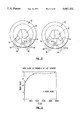
- FIG. 1 is a schematic representation of a rotating cylindrical magnetron sputtering system for deposition of dielectric films according to the present invention
- FIG. 2 is a cross-sectional view of dual cathode assemblies
- FIG. 3 is a graph of Taber score vs. thickness of a SiO 2 overcoat produced with the inventive method
- FIG. 4 is a graph comparing the percent reflectance of glass coated with a multi-layer Si 3 N 4 and SiO 2 film with the percent reflectance of uncoated glass;
- FIG. 5 is a graph illustrating the percent reflectance of glass coated with a multi-layer film of Si 3 N 4 and SiO 2 , burnished and unburnished;
- FIG. 6 is a graph comparing the percent reflectance of glass coated on both sides with a multi-layer film of Si 3 N 4 and SiO 2 , burnished and unburnished;
- FIG. 7 shows the percent reflectance of a multi-layer coating consisting of Al-SiO 2 -TiO 2 -SiO 2 -TiO 2 films over the visible spectrum of light.
- a plasma is formed in an enclosed reaction chamber 10, in which a vacuum is maintained, where a substrate, such as substrate 12, is placed for depositing a thin film of material upon it.
- the substrate 12 can be any vacuum compatible material, such as metal, glass, and some plastics.
- the film can also be deposited over other films or coatings that have previously been formed on a substrate surface.
- the cathode assembly 14 comprises generally an elongated cylindrical tube 16 mounted in the reaction chamber 10.
- An elongated magnet assembly 18 is carried within a lower portion of the tube 16, extends substantially its entire length, and is restrained against rotation with it.
- the tube 16 is preferable cooled by passing water or another heat transfer fluid through it.
- the tube 16 is formed of a suitable nonmagnetic material such as, for example, brass or stainless steel, and is of a diameter, wall thickness and length required for a particular operation to be performed. Applied to the outer surface of the tube 16 is a layer of a selected target material 20 to be deposited onto the substrate 12 being coated. In order to deposit a silicon based film on the substrate 12, this target material is pure silicon that is doped with a small percentage of a conductive material, such as aluminum, boron, antimony, phosphorus or arsenic, in order to render the target surface electrically conductive.
- the amount of dopant can be as high as approximately 10%, although less than 6% is better. The preferred amount is approximately as near zero as possible while achieving the necessary electrical conductivity.
- a concentration of approximately 2% is practically achieved by plasma spray techniques.
- the target material 20 is preferably applied to the core tube 16 by plasma spraying
- the tube 16 and the layer of coating material 20 constitute a tubular target or sputtering source as distinguished from the convention planar target.
- the tube 16 is supported in a manner to be rotated about its longitudinal axis by a target drive system 22.
- the orientation of the longitudinal axis depends upon the shape and position of the substrate that is being coated. In the example being described herein, the substrate 12 is held horizontally and is flat, and the longitudinal axis of the tube 16 is also horizontal, thus being parallel with the substrate surface to be coated.
- the tube 16 is rotatably held at each end in a horizontal position.
- a support structure at one end also allows cooling fluid to be introduced into the tube 16 and withdrawn from it, and contains a mechanism for driving the tube 16 from a motor source outside of the vacuum chamber 10. Rotating seals are included in this support structure for isolating the cooling fluid from the vacuum chamber.
- a support structure at an opposite end includes an electrical brush assembly for connecting the tube to a negative voltage.
- the magnetic assembly 18 comprises an array of magnetic poles arranged in straight parallel rows along the length of the tube 16. Each row has three alternating magnetic poles 24, 26 and 28. In one configuration, the poles 24, 26 and 28 are arranged to have respective north, south and north polarities. An opposite configuration of respective south, north and south polarities may also be used. In either case, the magnetic poles 24, 26 and 28 are positioned in relation to the tube 16 so that their lines of force run from one pole, through the tube 16, and back through the tube in a curved path to an adjacent pole having an opposite polarity. This arrangement generates what is called a magnetic tunnel, which not only allows the sputtering rate to be increased, but also causes the target material 20 to be removed faster inside the tunnel, especially in the middle of this magnetic pattern.
- the arrangement of the magnetic assembly 18 in FIG. 1 is a "W" configuration of three elongated magnets 24, 26 and 28.
- An alternative is a "U” configuration wherein a single magnet is position in the middle and a "U” shaped piece of magnetic material is positioned to form poles on either side of the magnet and of opposite polarity. In either case, it is usually desireable to position the pole faces as close to an inner surface of the tube 16 as possible.
- the magnetic assembly 18 is preferably supported within the tube 16 from a stationary axial rod or cooling fluid tube, or is held away from the inner surface of the tube 16 by rollers that are carried by the magnetic assembly 18, or both.
- a cathode potential V sufficient to cause sputtering to occur is supplied to the tubular target 20 from a DC power source 30 through a power line 32 having sliding contact 34 with the tube 16 by a conventional electrical brush.
- the enclosure of the reaction chamber 10 is conductive and electrically grounded. It serves as an anode in the sputtering process.
- a separate anode may be optionally employed and maintained at a small positive voltage.
- Such an anode is a plane positioned above the target tube surface 20 and is preferably water cooled in order that high power levels may be employed.
- the reaction chamber 10 is provided with an outlet tube 36 communicating with a vacuum pump 38.
- a gas supply system is included.
- a first gas supply tube 40 extends into the coating chamber 10 and from a source 42 of an inert gas.
- the inert gas is preferably argon for the specific methods being described.
- Nozzles 44 connected to inlet tube 40 distribute the inert gas in a region above the rotating cathode 14. It is the inert gas that breaks down into electrically charged ions under the influence of an electric field established between the target surface 20 and the grounded chamber enclosure or separate floating anode.
- the positive ions are attracted to and bombard the target surface 20, under the influence of the electric field, in an area to which they are guided by the magnetic field. This bombardment occurs primarily in two parallel strips, one between each of the opposing magnetic poles, along the length of the cylinder 14 at its bottom, opposite the magnet assembly 18.
- the tube 16 is rotated, its target surface 20 is rotated through these two parallel strips.
- a second gas supply tube 46 extends through the coating chamber 10 from a reactive gas source 48.
- the reactive gas is chosen to be pure oxygen.
- a nitride film is to be deposited, such as silicon nitride, the reactive gas is chosen to be pure nitrogen.
- the reactive gas is selected from hydrocarbon gases.
- Nozzles 50 connected to inlet tube 46 distribute the reactant gas close to and across the width of the substrate 12 being coated. Molecules of the reactive gas combine with molecules sputtered from the target surface, as a result of ion bombardment, to form the desired molecules that are deposited on the top surface of the substrate 12.
- silicon oxide films are deposited by use of the silicon material cylindrical target surface 20 and oxygen as the reactive gas.
- the inert and reactive gases from the sources 42 and 48 can be combined and delivered into the chamber 10 through a common tube and set of nozzles.
- the delivery tube is preferably positioned along a side of the rotating target tube 16 and parallel with its longitudinal axis. Two such tubes can be used, one on each side of the target tube 16 and parallel with its longitudinal axis, each delivering the same combination of inert and reactive gases.
- more than one reactive gas can be simultaneously supplied, depending upon the film being deposited. An example is to supply both oxygen and nitrogen in order to coat the substrate 12 with a silicon oxynitride film.
- the film being formed does apparently become deposited on a surface portion of the target 20 after it leaves the region below the stationary magnetic structure 18, in the same manner as occurs on a planar magnetron target surface. But it has been found that this is no problem because the deposited film apparently is removed by the sputtering process when that surface portion again rotates through the region below the magnetic structure 18. It has also been found that this removal does not impair the quality of the film formed on the substrate 12, nor does it impact on the rate of deposition of the film.
- the film is, however, deposited on other surfaces within the chamber 10 that are maintained at the large negative potential of the target surface 20.
- Such surfaces can exist in the supporting structures of the tube 16. If they do, it is highly desireable to cover them with a dielectric so that any deposited films will not have the large voltage surface immediately behind them and arcing will be avoided. If a positive voltage, floating anode is used, its surface is shaped and positioned away from such negative voltage surfaces in order to draw the plasma away from them and thus reduce deposition on them.
- FIG. 1 shows a single target assembly for simplicity, but it may be preferred to position two or more such assemblies adjacent each other with their tube longitudinal axes being parallel. This can result in an increased rate of deposition.
- FIG. 2 shows a cross-section view of dual cathode assemblies. It may be preferred, for large scale machines, that the magnetic poles of adjacent target assemblies which face each other be of opposite polarity. This restrains the plasma from extending upward between adjacent target assemblies. In this embodiment, the magnetic poles alternate in polarity so that if pole 28 is north, pole 52 is south, or vice-versa. As described previously, the magnetic field lines of flux 58 generate a magnetic tunnel wherein the sputtering is concentrated. Points 60 and 62 denote the approximate outer boundaries of the tunnel in one assembly and points 64 and 66 denote the approximate outer boundaries of the other.
- the method according to the invention provides durable silicon based compound coatings which can be deposited at relatively high rates.
- films of silicon oxide (SiO 2 ) and Si 3 N 4 were prepared on different substrates and were tested for their mechanical and optical properties and deposition rates. It is known that SiO 2 is the predominant form of silicon oxide created in the sputtering process. However, it is believed that other forms are produced as well. Thus, unless otherwise stated, SiO 2 will represent all forms of silicon oxide produced by the inventive method. In addition, by utilizing reactive gas mixtures more complex silicon compounds are sputtered.
- Si x O y N z is deposited, where x, y and z represent different stoichiometric amounts of silicon, oxygen, and nitrogen of the various compounds formed. Furthermore, by regulating the process conditions, particularly the flow rates of oxygen and nitrogen and the pressure of the reaction chamber, x, y and z can be controlled.
- Both systems use untrapped diffusion pumps that achieved a base pressure in the 10 -6 Torr range before operation.
- Argon was used as an inert gas and either oxygen or nitrogen was used as the reactant gas.
- the partial pressure of the gases was determined by the transition from the oxide or nitride mode to the metallic mode. Experiments were run as close to that transition as practicable.
- the pressure and flow rate of the sputtering gases were controlled by conventional devices.
- Each sputtering source was connected to an appropriate direct current power source having provision for automatically maintaining the voltage, current or power, as desired.
- the silicon target was impregnated or doped with a small amount of aluminum in the range of from 2-4%.
- the target was prepared by plasma spray.
- the film deposited according to the invention contains reaction products of aluminum and silicon with the reactive gas.
- the reactive gas was oxygen
- the deposition coating contained a mixture of aluminum and silicon oxides. It is believed that the percentage of aluminum oxides in the film is approximately equal to the percentage of aluminum in the target. The amount of aluminum oxides increases proportionally with the amount of aluminum in the target.
- the coating contained a mixture of aluminum and silicon nitrides. All of these four components are relatively hard and form an amorphous film that acts as a strong barrier.
- the target was conditioned using an inert gas, then the process gas was added until the desired partial pressure was reached. The process was operated at that point until the process was stabilized. The substrates were then introduced to the coat zone and the film was applied.
- the substrate used was typically soda lime glass, but, depending on the test, could be any combination of the following: microscope slide, Corning 7059 glass, 0.5 mil PET (poly(ethylene terephthalate)) film, fused silica stressed disc or carbon planchet.
- Deposition Rate The deposition rates for the production of SiO 2 and Si 3 N 4 utilizing the inventive method were measured and compared with deposition rates of other films applying the same process.
- DDR dynamic deposition rate
- n Number of passes.
- Abrasion Resistance The durability of SiO 2 films and Si 3 N 4 produced by the inventive method was measured with a Taber Abrader.
- a CS10F wheel with 500 gram weights was used.
- the area of the abrade was observed through a microscope at 50 times magnification and a picture was taken.
- Four 1" ⁇ 1" squares were drawn on the picture in random places and the number of scratches inside these squares was counted. The number of scratches in all four squares was averaged and the part was given a Taber score based on the following formula:
- the Taber score is a linear scale where no scratches is a 10, and 50 scratches is a 0.
- uncoated soda lime glass typically scores about 9.0.
- Silicon oxide films of different thicknesses were coated on VWR (Vanwater and Rogers Co.) slides.
- the cathode was run at 2.0 kW and the line speed was 20"/min.
- the other operating conditions of the cylindrical magnetron were comparable to those set forth in Table 1 below.
- 4" ⁇ 4" samples were cut from each run for Taber Abrader tests. The results indicate that a 900 ⁇ thick sample had a Taber score of 9.40 and a 3000 ⁇ sample had a Taber score of 9.70.
- FTIR analysis showed the film to be relatively pure and free of contamination.
- SEM cross-section analysis showed that the SiO 2 was dense and amorphous.
- FIG. 3 graphically illustrates the above results.
- SiO 2 as a Barrier Layer On a 6" ⁇ 6" PET sample, a 3000 ⁇ film of SiO 2 was prepared.
- the substrate sample was passed through the plasma 16 times.
- Table 1 sets forth the process data for production of the oxide. Beginning at zero, Time refers to the lapsed time in the process.
- the Potential refers to the potential between the cathode assembly tube and the ground.
- the Power refers to the power supplied and the Current was measured at the power source.
- the flow rates of the inert gas (Ar) and reactive gas (O 2 ) were measured in standard cubic centimeters per minute (SCCM).
- SCCM standard cubic centimeters per minute
- the Pressure of the reaction chamber is measured in microns.
- the Number of Passes refers to the number of times the substrate had crossed the plasma during the sputtering process at a particular time. For instance, at time 23 minutes into the process, the substrate was making its 13th pass.
- Water permeation testing was done on a Mocon Permatran and oxygen testing was done on a Mocon Ox-Tran Twin. In one test, approximately 3000 ⁇ of SiO 2 was applied to a 6" ⁇ 6" ⁇ 0.5 mil PET sample. This was tested for water permeation, an uncoated sample had a measured transfer of 43.4 grams/m 2 /day while the coated sample only had a transfer of 3.3 grams/m 2 /day.
- Curve 68 in FIG. 4 is the percent reflectance of the uncoated glass substrate.
- Curve 70 is the percent reflectance of the multi-layer film.
- Curve 72 of FIG. 5 is the percent reflectance of the unburnished film.
- Curve 74 is the percent reflectance of the burnished film.
- Curve 76 of FIG. 6 is the percent reflectance of an unburnished film.
- Curve 78 is the percent reflectance of the burnished film.
- Enhanced Aluminum Mirrors On a glass substrate, a five layer coating consisting of a single aluminum film followed by alternative layers of SiO 2 and TiO 2 was prepared. Table 4 sets forth the process data for the production of the aluminum and oxide films.
- FIG. 7 is a graph of the percent reflectance of the film measured against the wavelength of radiation over the visible spectrum. Reflectance was measured at a six (6) degree angle of incidence.
Abstract
Description
DDR(Åmm.sup.2 /Joule)=(d*C*S)/(P*n)
______________________________________
        Film  DDR
______________________________________
        SiO.sub.2
              700-1100
        Si.sub.3 N.sub.4
              900-1400
______________________________________
TABER SCORE=#SCRATCHES*(-0.18)+10
______________________________________
           Cylindrical Magnetron
                           Planar
Compound   Taber Score     Taber Score
______________________________________
SiO.sub.2   9.6 ± .2    9.55 ± .2*
Si.sub.3 N.sub.4
           9.45 ± .3     9.3 ± .6*
TiO.sub.2  8.5             8.5
______________________________________
 *The planar silicon compounds were produced using an RF enhanced system.
______________________________________
SiO.sub.2 Thickness (Å)
                 Taber Score
______________________________________
uncoated         3.57
 445             6.94
1063             7.93
3000             9.37
8250             9.55
9600             9.76
______________________________________
              TABLE 1
______________________________________
              Poten-  Cur-             Pres-
Time  Power   tial    rent SCCM  SCCM  sure  No.
(min) (kW)    (V)     (A)  O.sub.2
                                 Ar    (μ)
                                             Passes
______________________________________
 0    3.0     481     6.30 10    23    0.98   1
 6    3.0     500     6.06 10    23    1.10   4
13    3.0     490     6.18 10    23    0.99   7
17    3.0     500     6.14 10    23    1.09  10
23    3.0     503     6.06 10    23    1.05  13
31    3.0     506     6.02 10    23    1.10  16
                 Total No. of Passes:
                             16
______________________________________
______________________________________
Index of refraction at 520 nm
                         1.46
% Transmittance (integrated D65 source)*
                         91.98
% Reflectance (single surface
                         3.42
integrated D65 source)**
% Absorbance             0.70
                  (or 8.48 × 10.sup.-6 % A/Å)
______________________________________
 *The uncoated slide had a % transmittance of 92.27
 **The uncoated slide had a % Reflectance of 3.83.
              TABLE 2
______________________________________
      Thick-           Cur- Pres-
      ness    Potential
                       rent sure No.   Substrate Speed
Layer (Å) (V)      (A)  (μ)
                                 Passes
                                       (in./min.)
______________________________________
Si.sub.3 N.sub.4
      180     670      2.99 1.18  2    31.6
SiO.sub.2
      250     501      4.00 1.02  3    21.8
Si.sub.3 N.sub.4
      1375    670      3.00 1.15 10    20.7
SiO.sub.2
      750     510      3.96 1.07 10    22.9
______________________________________
              TABLE 3
______________________________________
      Thick-  Po-           Cur- Pres-      Substrate
      ness    tential Power rent sure No.   Speed
Layer (Å) (V)     (kW)  (A)  (μ)
                                      Passes
                                            (in/min)
______________________________________
TiO.sub.2
      130     468     40    92   3.0   1     22
SiO.sub.2
      283     364     11.5  32   1.5   1     20
TiO.sub.2
      1132    465     40    93   3.0  44    120
SiO.sub.2
      861     365     10    27   1.5  26    160
______________________________________
              TABLE 4
______________________________________
      Thick-  Po-           Cur- Pres-      Substrate
      ness    tential Power rent sure No.   Speed
Layer (Å) (V)     (kW)  (A)  (μ)
                                      Passes
                                            (in/min)
______________________________________
Al    650     512     30    55   1.5   1     88
SiO.sub.2
      797     369     10    28   1.5  25    160
TiO.sub.2
      510     449     40    96   1.5  22    130
SiO.sub.2
      949     368     10    28   1.5  36    160
TiO.sub.2
      532     452     40    96   1.5  23    130
______________________________________
Claims (13)
Priority Applications (11)
| Application Number | Priority Date | Filing Date | Title |
|---|---|---|---|
| US07/433,690 US5047131A (en) | 1989-11-08 | 1989-11-08 | Method for coating substrates with silicon based compounds |
| EP90917735A EP0502068B1 (en) | 1989-11-08 | 1990-11-07 | Method for coating substrates with silicon based compounds |
| JP50051491A JP3164364B2 (en) | 1989-11-08 | 1990-11-07 | Method of coating substrate with silicon-based compound |
| KR1019920701089A KR100199663B1 (en) | 1989-11-08 | 1990-11-07 | Method for coating substrates with silicon based compounds |
| AU68730/91A AU631710B2 (en) | 1989-11-08 | 1990-11-07 | Method for coating substrates with silicon based compounds |
| DE69018479T DE69018479T2 (en) | 1989-11-08 | 1990-11-07 | METHOD FOR COATING SUBSTRATES WITH SILICON-BASED CONNECTIONS. |
| PCT/US1990/006459 WO1991007519A1 (en) | 1989-11-08 | 1990-11-07 | Method for coating substrates with silicon based compounds |
| DK90917735.4T DK0502068T3 (en) | 1989-11-08 | 1990-11-07 | Process for coating substrates with silicon-based compounds |
| AT90917735T ATE120806T1 (en) | 1989-11-08 | 1990-11-07 | METHOD FOR COATING SUBSTRATES WITH SILICON-BASED COMPOUNDS. |
| CA002069329A CA2069329C (en) | 1989-11-08 | 1990-11-07 | Method for coating substrates with silicon based compounds |
| ES90917735T ES2070343T3 (en) | 1989-11-08 | 1990-11-07 | METHOD FOR COATING SUBSTRATES WITH SILICON-BASED COMPOUNDS. |
Applications Claiming Priority (1)
| Application Number | Priority Date | Filing Date | Title |
|---|---|---|---|
| US07/433,690 US5047131A (en) | 1989-11-08 | 1989-11-08 | Method for coating substrates with silicon based compounds |
Publications (1)
| Publication Number | Publication Date |
|---|---|
| US5047131A true US5047131A (en) | 1991-09-10 |
Family
ID=23721176
Family Applications (1)
| Application Number | Title | Priority Date | Filing Date |
|---|---|---|---|
| US07/433,690 Expired - Lifetime US5047131A (en) | 1989-11-08 | 1989-11-08 | Method for coating substrates with silicon based compounds |
Country Status (11)
| Country | Link |
|---|---|
| US (1) | US5047131A (en) |
| EP (1) | EP0502068B1 (en) |
| JP (1) | JP3164364B2 (en) |
| KR (1) | KR100199663B1 (en) |
| AT (1) | ATE120806T1 (en) |
| AU (1) | AU631710B2 (en) |
| CA (1) | CA2069329C (en) |
| DE (1) | DE69018479T2 (en) |
| DK (1) | DK0502068T3 (en) |
| ES (1) | ES2070343T3 (en) |
| WO (1) | WO1991007519A1 (en) |
Cited By (96)
| Publication number | Priority date | Publication date | Assignee | Title |
|---|---|---|---|---|
| WO1992009718A1 (en) * | 1990-11-21 | 1992-06-11 | Viratec Thin Films, Inc. | Anode structures for magnetron sputtering apparatus |
| US5158660A (en) * | 1990-06-08 | 1992-10-27 | Saint-Gobain Vitrage International | Rotary sputtering cathode |
| US5171411A (en) * | 1991-05-21 | 1992-12-15 | The Boc Group, Inc. | Rotating cylindrical magnetron structure with self supporting zinc alloy target |
| EP0560534A1 (en) * | 1992-03-04 | 1993-09-15 | The Boc Group, Inc. | Interference filters |
| US5364518A (en) * | 1991-05-28 | 1994-11-15 | Leybold Aktiengesellschaft | Magnetron cathode for a rotating target |
| US5377045A (en) * | 1990-05-10 | 1994-12-27 | The Boc Group, Inc. | Durable low-emissivity solar control thin film coating |
| US5384021A (en) * | 1991-10-11 | 1995-01-24 | The Boc Group Plc | Sputtering apparatus |
| US5403458A (en) * | 1993-08-05 | 1995-04-04 | Guardian Industries Corp. | Sputter-coating target and method of use |
| US5425860A (en) * | 1993-04-07 | 1995-06-20 | The Regents Of The University Of California | Pulsed energy synthesis and doping of silicon carbide |
| US5427665A (en) * | 1990-07-11 | 1995-06-27 | Leybold Aktiengesellschaft | Process and apparatus for reactive coating of a substrate |
| US5470452A (en) * | 1990-08-10 | 1995-11-28 | Viratec Thin Films, Inc. | Shielding for arc suppression in rotating magnetron sputtering systems |
| EP0691553A2 (en) | 1994-07-07 | 1996-01-10 | The Boc Group, Inc. | Thin film filters |
| US5487821A (en) * | 1993-07-01 | 1996-01-30 | The Boc Group, Inc. | Anode structure for magnetron sputtering systems |
| EP0700720A1 (en) | 1994-09-06 | 1996-03-13 | Becton, Dickinson and Company | Plastic articles of reduced gas transmission and method therefor |
| US5527389A (en) * | 1992-08-07 | 1996-06-18 | Ase Americas, Inc. | Apparatus for forming diffusion junctions in solar cell substrates |
| US5563734A (en) * | 1993-04-28 | 1996-10-08 | The Boc Group, Inc. | Durable low-emissivity solar control thin film coating |
| US5616225A (en) * | 1994-03-23 | 1997-04-01 | The Boc Group, Inc. | Use of multiple anodes in a magnetron for improving the uniformity of its plasma |
| US5814195A (en) * | 1995-04-25 | 1998-09-29 | The Boc Group, Inc. | Sputtering system using cylindrical rotating magnetron electrically powered using alternating current |
| US5830579A (en) * | 1994-01-07 | 1998-11-03 | Societe Anonyme De Traitment Des Metaux Et Alliages Company (Satma) | Strip based on coated aluminum, which is resistant to corrosion and is deformable |
| US5853816A (en) * | 1992-07-15 | 1998-12-29 | Emiel Vanderstraeten | Method of coating a sputter cathode with a layer of material to be applied to a substrate by sputtering |
| US5891556A (en) * | 1995-02-23 | 1999-04-06 | Saint-Gobain Vitrage | Transparent substrate with antireflection coating |
| US5946013A (en) * | 1992-12-22 | 1999-08-31 | Canon Kabushiki Kaisha | Ink jet head having a protective layer with a controlled argon content |
| US6074730A (en) * | 1997-12-31 | 2000-06-13 | The Boc Group, Inc. | Broad-band antireflection coating having four sputtered layers |
| US6352626B1 (en) | 1999-04-19 | 2002-03-05 | Von Zweck Heimart | Sputter ion source for boron and other targets |
| US6375814B1 (en) * | 1998-04-16 | 2002-04-23 | Sinvaco N.V. | Magnetron with parallel race track and modified end portions thereof |
| WO2002038826A1 (en) * | 2000-11-09 | 2002-05-16 | Viratec Thin Films, Inc. | Alternating current rotatable sputter cathode |
| US6392239B1 (en) | 1996-12-30 | 2002-05-21 | Jan Kuklinski | Optical array converting UV radiation |
| US6391400B1 (en) | 1998-04-08 | 2002-05-21 | Thomas A. Russell | Thermal control films suitable for use in glazing |
| US6436252B1 (en) | 2000-04-07 | 2002-08-20 | Surface Engineered Products Corp. | Method and apparatus for magnetron sputtering |
| US6497803B2 (en) * | 2000-05-31 | 2002-12-24 | Isoflux, Inc. | Unbalanced plasma generating apparatus having cylindrical symmetry |
| US20030053784A1 (en) * | 2001-09-19 | 2003-03-20 | Labrake Dwayne L. | Optical and optoelectronic articles |
| US6589657B2 (en) | 2001-08-31 | 2003-07-08 | Von Ardenne Anlagentechnik Gmbh | Anti-reflection coatings and associated methods |
| US6602587B2 (en) * | 1994-12-23 | 2003-08-05 | Saint-Gobain Glass France | Glass substrates coated with a stack of thin layers having reflective properties in the infra-red and/or solar ranges |
| US6614085B2 (en) | 1997-08-21 | 2003-09-02 | Micron Technology, Inc. | Antireflective coating layer |
| US20030184893A1 (en) * | 2002-03-29 | 2003-10-02 | Ritek Corporation | Multi-layer mirror and fabricating method thereof |
| US6652974B1 (en) | 1999-05-18 | 2003-11-25 | Cardinal Ig Company | Hard, scratch-resistant coatings for substrates |
| US6660365B1 (en) | 1998-12-21 | 2003-12-09 | Cardinal Cg Company | Soil-resistant coating for glass surfaces |
| US6736948B2 (en) | 2002-01-18 | 2004-05-18 | Von Ardenne Anlagentechnik Gmbh | Cylindrical AC/DC magnetron with compliant drive system and improved electrical and thermal isolation |
| US6749813B1 (en) | 2000-03-05 | 2004-06-15 | 3M Innovative Properties Company | Fluid handling devices with diamond-like films |
| US20040129561A1 (en) * | 2003-01-07 | 2004-07-08 | Von Ardenne Anlagentechnik Gmbh | Cylindrical magnetron magnetic array mid span support |
| US20040140208A1 (en) * | 2001-06-14 | 2004-07-22 | German John R. | Alternating current rotatable sputter cathode |
| US20040163945A1 (en) * | 2002-12-18 | 2004-08-26 | Klaus Hartig | Plasma-enhanced film deposition |
| US20040163943A1 (en) * | 2003-02-21 | 2004-08-26 | Rietzel James G. | Cylindrical magnetron with self cleaning target |
| US20040200418A1 (en) * | 2003-01-03 | 2004-10-14 | Klaus Hartig | Plasma spray systems and methods of uniformly coating rotary cylindrical targets |
| US20050025982A1 (en) * | 1998-12-21 | 2005-02-03 | Cardinal Cg Company | Soil-resistant coating for glass surfaces |
| US20050051422A1 (en) * | 2003-02-21 | 2005-03-10 | Rietzel James G. | Cylindrical magnetron with self cleaning target |
| US20050224343A1 (en) * | 2004-04-08 | 2005-10-13 | Richard Newcomb | Power coupling for high-power sputtering |
| US6974629B1 (en) | 1999-08-06 | 2005-12-13 | Cardinal Cg Company | Low-emissivity, soil-resistant coating for glass surfaces |
| US20060049043A1 (en) * | 2004-08-17 | 2006-03-09 | Matuska Neal W | Magnetron assembly |
| US20060065524A1 (en) * | 2004-09-30 | 2006-03-30 | Richard Newcomb | Non-bonded rotatable targets for sputtering |
| US20060096855A1 (en) * | 2004-11-05 | 2006-05-11 | Richard Newcomb | Cathode arrangement for atomizing a rotatable target pipe |
| US20060278521A1 (en) * | 2005-06-14 | 2006-12-14 | Stowell Michael W | System and method for controlling ion density and energy using modulated power signals |
| US20060278524A1 (en) * | 2005-06-14 | 2006-12-14 | Stowell Michael W | System and method for modulating power signals to control sputtering |
| US20060278519A1 (en) * | 2005-06-10 | 2006-12-14 | Leszek Malaszewski | Adaptable fixation for cylindrical magnetrons |
| US7198832B2 (en) | 1999-10-25 | 2007-04-03 | Vitex Systems, Inc. | Method for edge sealing barrier films |
| US20070095281A1 (en) * | 2005-11-01 | 2007-05-03 | Stowell Michael W | System and method for power function ramping of microwave liner discharge sources |
| US20070098893A1 (en) * | 2005-11-01 | 2007-05-03 | Stowell Michael W | Coated substrate created by systems and methods for modulation of power and power related functions of PECVD discharge sources to achieve new film properties |
| US20070212893A1 (en) * | 2006-03-07 | 2007-09-13 | Mcteer Allen | System and method for sputtering a tensile silicon nitride film |
| US20070248756A1 (en) * | 2006-04-19 | 2007-10-25 | Cardinal Cg Company | Opposed functional coatings having comparable single surface reflectances |
| US7294404B2 (en) | 2003-12-22 | 2007-11-13 | Cardinal Cg Company | Graded photocatalytic coatings |
| US20080138502A1 (en) * | 2006-12-11 | 2008-06-12 | Roland Trassl | Method for the production of an sin:h layer on a substrate |
| USRE40531E1 (en) | 1999-10-25 | 2008-10-07 | Battelle Memorial Institute | Ultrabarrier substrates |
| US20090023254A1 (en) * | 2007-07-20 | 2009-01-22 | Joo-Soo Lim | Method of forming inorganic insulating layer and method of fabricating array substrate for display device using the same |
| US7510913B2 (en) | 2003-04-11 | 2009-03-31 | Vitex Systems, Inc. | Method of making an encapsulated plasma sensitive device |
| USRE40787E1 (en) | 1999-10-25 | 2009-06-23 | Battelle Memorial Institute | Multilayer plastic substrates |
| US7604865B2 (en) | 2004-07-12 | 2009-10-20 | Cardinal Cg Company | Low-maintenance coatings |
| US7648925B2 (en) | 2003-04-11 | 2010-01-19 | Vitex Systems, Inc. | Multilayer barrier stacks and methods of making multilayer barrier stacks |
| US20100018854A1 (en) * | 2008-07-24 | 2010-01-28 | Seagate Technology Llc | Trim magnets to adjust erosion rate of cylindrical sputter targets |
| US7695590B2 (en) | 2004-03-26 | 2010-04-13 | Applied Materials, Inc. | Chemical vapor deposition plasma reactor having plural ion shower grids |
| US7767498B2 (en) | 2005-08-25 | 2010-08-03 | Vitex Systems, Inc. | Encapsulated devices and method of making |
| US7767561B2 (en) | 2004-07-20 | 2010-08-03 | Applied Materials, Inc. | Plasma immersion ion implantation reactor having an ion shower grid |
| US20100243428A1 (en) * | 2009-03-27 | 2010-09-30 | Sputtering Components, Inc. | Rotary cathode for magnetron sputtering apparatus |
| US7820309B2 (en) | 2007-09-14 | 2010-10-26 | Cardinal Cg Company | Low-maintenance coatings, and methods for producing low-maintenance coatings |
| US7862910B2 (en) | 2006-04-11 | 2011-01-04 | Cardinal Cg Company | Photocatalytic coatings having improved low-maintenance properties |
| US20110053355A1 (en) * | 2009-09-03 | 2011-03-03 | Chunghwa Picture Tubes, Ltd. | Plasma apparatus and method of fabricating nano-crystalline silicon thin film |
| US7923114B2 (en) | 2004-12-03 | 2011-04-12 | Cardinal Cg Company | Hydrophilic coatings, methods for depositing hydrophilic coatings, and improved deposition technology for thin films |
| US20110127157A1 (en) * | 2007-08-15 | 2011-06-02 | Gencoa Ltd. | Low impedance plasma |
| US8058156B2 (en) | 2004-07-20 | 2011-11-15 | Applied Materials, Inc. | Plasma immersion ion implantation reactor having multiple ion shower grids |
| US8092660B2 (en) | 2004-12-03 | 2012-01-10 | Cardinal Cg Company | Methods and equipment for depositing hydrophilic coatings, and deposition technologies for thin films |
| WO2012094566A2 (en) | 2011-01-06 | 2012-07-12 | Sputtering Components, Inc. | Sputtering apparatus |
| US20120174864A1 (en) * | 2009-10-05 | 2012-07-12 | Kabushiki Kaisha Kobe Seiko Sho (Kobe Steel, Ltd.) | Plasma cvd apparatus |
| US8590338B2 (en) | 2009-12-31 | 2013-11-26 | Samsung Mobile Display Co., Ltd. | Evaporator with internal restriction |
| WO2014039426A1 (en) | 2012-09-04 | 2014-03-13 | Sputtering Components, Inc. | Sputtering apparatus |
| US8808457B2 (en) * | 2002-04-15 | 2014-08-19 | Samsung Display Co., Ltd. | Apparatus for depositing a multilayer coating on discrete sheets |
| US8900366B2 (en) | 2002-04-15 | 2014-12-02 | Samsung Display Co., Ltd. | Apparatus for depositing a multilayer coating on discrete sheets |
| US8955217B2 (en) | 1999-10-25 | 2015-02-17 | Samsung Display Co., Ltd. | Method for edge sealing barrier films |
| US9184410B2 (en) | 2008-12-22 | 2015-11-10 | Samsung Display Co., Ltd. | Encapsulated white OLEDs having enhanced optical output |
| US9312108B2 (en) | 2013-03-01 | 2016-04-12 | Sputtering Components, Inc. | Sputtering apparatus |
| US9337446B2 (en) | 2008-12-22 | 2016-05-10 | Samsung Display Co., Ltd. | Encapsulated RGB OLEDs having enhanced optical output |
| US9388490B2 (en) | 2009-10-26 | 2016-07-12 | General Plasma, Inc. | Rotary magnetron magnet bar and apparatus containing the same for high target utilization |
| US9418823B2 (en) | 2013-03-01 | 2016-08-16 | Sputtering Components, Inc. | Sputtering apparatus |
| US20170038350A1 (en) * | 2010-03-26 | 2017-02-09 | Waters Technologies Corporation | Chromatography apparatus having diffusion-bonded and surface-modified components |
| US9738967B2 (en) | 2006-07-12 | 2017-08-22 | Cardinal Cg Company | Sputtering apparatus including target mounting and control |
| US10604442B2 (en) | 2016-11-17 | 2020-03-31 | Cardinal Cg Company | Static-dissipative coating technology |
| US10950821B2 (en) | 2007-01-26 | 2021-03-16 | Samsung Display Co., Ltd. | Method of encapsulating an environmentally sensitive device |
| WO2022008048A1 (en) | 2020-07-08 | 2022-01-13 | Toyota Motor Europe | Contaminated hydrogen gas composition and its use as a reference for hydrogen fuels |
Families Citing this family (5)
| Publication number | Priority date | Publication date | Assignee | Title |
|---|---|---|---|---|
| JPH0586462A (en) * | 1991-06-28 | 1993-04-06 | Mitsubishi Materials Corp | Target for sputtering and its manufacture |
| DE19615242A1 (en) * | 1996-04-18 | 1997-10-23 | Daimler Benz Ag | Coating plastic surface, especially of electronics housing |
| TW347369B (en) * | 1996-12-17 | 1998-12-11 | Asahi Glass Co Ltd | Organic substrate provided with a light absorptive antireflection film and process for production |
| JP2000239827A (en) * | 1998-12-22 | 2000-09-05 | Bridgestone Corp | Laminated structural body and its production |
| EP1251188B1 (en) | 1999-10-13 | 2008-01-09 | AGC Ceramics Co., Ltd. | Sputtering target and method for preparing the same and film-forming method |
Citations (21)
| Publication number | Priority date | Publication date | Assignee | Title |
|---|---|---|---|---|
| US3798146A (en) * | 1973-06-06 | 1974-03-19 | Shatterproof Glass Corp | Method of making a transparent article having reduced radiation transmittance |
| US3826728A (en) * | 1970-05-20 | 1974-07-30 | Shatterproof Glass Corp | Transparent article having reduced solar radiation transmittance and method of making the same |
| US3956093A (en) * | 1974-12-16 | 1976-05-11 | Airco, Inc. | Planar magnetron sputtering method and apparatus |
| US4013532A (en) * | 1975-03-03 | 1977-03-22 | Airco, Inc. | Method for coating a substrate |
| US4022947A (en) * | 1975-11-06 | 1977-05-10 | Airco, Inc. | Transparent panel having high reflectivity for solar radiation and a method for preparing same |
| US4046659A (en) * | 1974-05-10 | 1977-09-06 | Airco, Inc. | Method for coating a substrate |
| US4125466A (en) * | 1976-05-18 | 1978-11-14 | Toyo Soda Manufacturing Co., Ltd. | Treatment of sludge comprising biological aggregate |
| US4131530A (en) * | 1977-07-05 | 1978-12-26 | Airco, Inc. | Sputtered chromium-alloy coating for plastic |
| US4166018A (en) * | 1974-01-31 | 1979-08-28 | Airco, Inc. | Sputtering process and apparatus |
| US4356073A (en) * | 1981-02-12 | 1982-10-26 | Shatterproof Glass Corporation | Magnetron cathode sputtering apparatus |
| US4417968A (en) * | 1983-03-21 | 1983-11-29 | Shatterproof Glass Corporation | Magnetron cathode sputtering apparatus |
| US4422916A (en) * | 1981-02-12 | 1983-12-27 | Shatterproof Glass Corporation | Magnetron cathode sputtering apparatus |
| US4426264A (en) * | 1980-12-13 | 1984-01-17 | Leybold Heraeus Gmbh | Method and means for controlling sputtering apparatus |
| US4443318A (en) * | 1983-08-17 | 1984-04-17 | Shatterproof Glass Corporation | Cathodic sputtering apparatus |
| US4445997A (en) * | 1983-08-17 | 1984-05-01 | Shatterproof Glass Corporation | Rotatable sputtering apparatus |
| US4466877A (en) * | 1983-10-11 | 1984-08-21 | Shatterproof Glass Corporation | Magnetron cathode sputtering apparatus |
| US4534841A (en) * | 1983-03-31 | 1985-08-13 | Leybold-Heraeus Gmbh | Solar controlled glazing and method of producing glazing |
| US4548691A (en) * | 1983-03-04 | 1985-10-22 | Leybold-Heraeus Gmbh | Thermally insulating glazing |
| WO1986007391A1 (en) * | 1985-06-14 | 1986-12-18 | Leybold-Heraeus Gmbh | An apparatus for coating substrates by plasma discharge |
| US4769291A (en) * | 1987-02-02 | 1988-09-06 | The Boc Group, Inc. | Transparent coatings by reactive sputtering |
| EP0165413B1 (en) * | 1984-05-12 | 1988-11-17 | Leybold Aktiengesellschaft | Process for the deposition of silicon compound optical layers by cathodic sputtering, and use of a formed silicon body as a target for this process |
-
1989
- 1989-11-08 US US07/433,690 patent/US5047131A/en not_active Expired - Lifetime
-
1990
- 1990-11-07 KR KR1019920701089A patent/KR100199663B1/en not_active IP Right Cessation
- 1990-11-07 CA CA002069329A patent/CA2069329C/en not_active Expired - Fee Related
- 1990-11-07 DK DK90917735.4T patent/DK0502068T3/en active
- 1990-11-07 ES ES90917735T patent/ES2070343T3/en not_active Expired - Lifetime
- 1990-11-07 JP JP50051491A patent/JP3164364B2/en not_active Expired - Fee Related
- 1990-11-07 EP EP90917735A patent/EP0502068B1/en not_active Expired - Lifetime
- 1990-11-07 DE DE69018479T patent/DE69018479T2/en not_active Expired - Fee Related
- 1990-11-07 AT AT90917735T patent/ATE120806T1/en not_active IP Right Cessation
- 1990-11-07 WO PCT/US1990/006459 patent/WO1991007519A1/en active IP Right Grant
- 1990-11-07 AU AU68730/91A patent/AU631710B2/en not_active Ceased
Patent Citations (23)
| Publication number | Priority date | Publication date | Assignee | Title |
|---|---|---|---|---|
| US3826728A (en) * | 1970-05-20 | 1974-07-30 | Shatterproof Glass Corp | Transparent article having reduced solar radiation transmittance and method of making the same |
| US3826728B1 (en) * | 1970-05-20 | 1986-06-10 | ||
| US3826728B2 (en) * | 1970-05-20 | 1994-07-12 | Boc Group Plc | Transparent article having reduced solar radiation transmittance and method of making same |
| US3798146A (en) * | 1973-06-06 | 1974-03-19 | Shatterproof Glass Corp | Method of making a transparent article having reduced radiation transmittance |
| US4166018A (en) * | 1974-01-31 | 1979-08-28 | Airco, Inc. | Sputtering process and apparatus |
| US4046659A (en) * | 1974-05-10 | 1977-09-06 | Airco, Inc. | Method for coating a substrate |
| US3956093A (en) * | 1974-12-16 | 1976-05-11 | Airco, Inc. | Planar magnetron sputtering method and apparatus |
| US4013532A (en) * | 1975-03-03 | 1977-03-22 | Airco, Inc. | Method for coating a substrate |
| US4022947A (en) * | 1975-11-06 | 1977-05-10 | Airco, Inc. | Transparent panel having high reflectivity for solar radiation and a method for preparing same |
| US4125466A (en) * | 1976-05-18 | 1978-11-14 | Toyo Soda Manufacturing Co., Ltd. | Treatment of sludge comprising biological aggregate |
| US4131530A (en) * | 1977-07-05 | 1978-12-26 | Airco, Inc. | Sputtered chromium-alloy coating for plastic |
| US4426264A (en) * | 1980-12-13 | 1984-01-17 | Leybold Heraeus Gmbh | Method and means for controlling sputtering apparatus |
| US4356073A (en) * | 1981-02-12 | 1982-10-26 | Shatterproof Glass Corporation | Magnetron cathode sputtering apparatus |
| US4422916A (en) * | 1981-02-12 | 1983-12-27 | Shatterproof Glass Corporation | Magnetron cathode sputtering apparatus |
| US4548691A (en) * | 1983-03-04 | 1985-10-22 | Leybold-Heraeus Gmbh | Thermally insulating glazing |
| US4417968A (en) * | 1983-03-21 | 1983-11-29 | Shatterproof Glass Corporation | Magnetron cathode sputtering apparatus |
| US4534841A (en) * | 1983-03-31 | 1985-08-13 | Leybold-Heraeus Gmbh | Solar controlled glazing and method of producing glazing |
| US4445997A (en) * | 1983-08-17 | 1984-05-01 | Shatterproof Glass Corporation | Rotatable sputtering apparatus |
| US4443318A (en) * | 1983-08-17 | 1984-04-17 | Shatterproof Glass Corporation | Cathodic sputtering apparatus |
| US4466877A (en) * | 1983-10-11 | 1984-08-21 | Shatterproof Glass Corporation | Magnetron cathode sputtering apparatus |
| EP0165413B1 (en) * | 1984-05-12 | 1988-11-17 | Leybold Aktiengesellschaft | Process for the deposition of silicon compound optical layers by cathodic sputtering, and use of a formed silicon body as a target for this process |
| WO1986007391A1 (en) * | 1985-06-14 | 1986-12-18 | Leybold-Heraeus Gmbh | An apparatus for coating substrates by plasma discharge |
| US4769291A (en) * | 1987-02-02 | 1988-09-06 | The Boc Group, Inc. | Transparent coatings by reactive sputtering |
Cited By (154)
| Publication number | Priority date | Publication date | Assignee | Title |
|---|---|---|---|---|
| US5377045A (en) * | 1990-05-10 | 1994-12-27 | The Boc Group, Inc. | Durable low-emissivity solar control thin film coating |
| US5158660A (en) * | 1990-06-08 | 1992-10-27 | Saint-Gobain Vitrage International | Rotary sputtering cathode |
| US5427665A (en) * | 1990-07-11 | 1995-06-27 | Leybold Aktiengesellschaft | Process and apparatus for reactive coating of a substrate |
| US5725746A (en) * | 1990-08-10 | 1998-03-10 | Viratec Thin Films, Inc. | Shielding for arc suppression in rotating magnetron sputtering systems |
| US5470452A (en) * | 1990-08-10 | 1995-11-28 | Viratec Thin Films, Inc. | Shielding for arc suppression in rotating magnetron sputtering systems |
| WO1992009718A1 (en) * | 1990-11-21 | 1992-06-11 | Viratec Thin Films, Inc. | Anode structures for magnetron sputtering apparatus |
| US5171411A (en) * | 1991-05-21 | 1992-12-15 | The Boc Group, Inc. | Rotating cylindrical magnetron structure with self supporting zinc alloy target |
| US5364518A (en) * | 1991-05-28 | 1994-11-15 | Leybold Aktiengesellschaft | Magnetron cathode for a rotating target |
| US5384021A (en) * | 1991-10-11 | 1995-01-24 | The Boc Group Plc | Sputtering apparatus |
| EP0560534A1 (en) * | 1992-03-04 | 1993-09-15 | The Boc Group, Inc. | Interference filters |
| US5853816A (en) * | 1992-07-15 | 1998-12-29 | Emiel Vanderstraeten | Method of coating a sputter cathode with a layer of material to be applied to a substrate by sputtering |
| US5527389A (en) * | 1992-08-07 | 1996-06-18 | Ase Americas, Inc. | Apparatus for forming diffusion junctions in solar cell substrates |
| US5946013A (en) * | 1992-12-22 | 1999-08-31 | Canon Kabushiki Kaisha | Ink jet head having a protective layer with a controlled argon content |
| US5425860A (en) * | 1993-04-07 | 1995-06-20 | The Regents Of The University Of California | Pulsed energy synthesis and doping of silicon carbide |
| US5563734A (en) * | 1993-04-28 | 1996-10-08 | The Boc Group, Inc. | Durable low-emissivity solar control thin film coating |
| US5487821A (en) * | 1993-07-01 | 1996-01-30 | The Boc Group, Inc. | Anode structure for magnetron sputtering systems |
| US5683558A (en) * | 1993-07-01 | 1997-11-04 | The Boc Group, Inc. | Anode structure for magnetron sputtering systems |
| US5403458A (en) * | 1993-08-05 | 1995-04-04 | Guardian Industries Corp. | Sputter-coating target and method of use |
| US5830579A (en) * | 1994-01-07 | 1998-11-03 | Societe Anonyme De Traitment Des Metaux Et Alliages Company (Satma) | Strip based on coated aluminum, which is resistant to corrosion and is deformable |
| US5616225A (en) * | 1994-03-23 | 1997-04-01 | The Boc Group, Inc. | Use of multiple anodes in a magnetron for improving the uniformity of its plasma |
| US5521765A (en) * | 1994-07-07 | 1996-05-28 | The Boc Group, Inc. | Electrically-conductive, contrast-selectable, contrast-improving filter |
| EP0691553A2 (en) | 1994-07-07 | 1996-01-10 | The Boc Group, Inc. | Thin film filters |
| US5510155A (en) * | 1994-09-06 | 1996-04-23 | Becton, Dickinson And Company | Method to reduce gas transmission |
| EP0700720A1 (en) | 1994-09-06 | 1996-03-13 | Becton, Dickinson and Company | Plastic articles of reduced gas transmission and method therefor |
| AU694530B2 (en) * | 1994-09-06 | 1998-07-23 | Becton Dickinson & Company | Plastic articles of reduced gas transmission and method therefor |
| US6602587B2 (en) * | 1994-12-23 | 2003-08-05 | Saint-Gobain Glass France | Glass substrates coated with a stack of thin layers having reflective properties in the infra-red and/or solar ranges |
| US20040241457A1 (en) * | 1994-12-23 | 2004-12-02 | Saint-Gobain Glass France | Glass substrates coated with a stack of thin layers having reflective properties in the infra-red and/or solar ranges |
| US6804048B2 (en) | 1994-12-23 | 2004-10-12 | Saint-Gobain Glass France | Glass substrates coated with a stack of thin layers having reflective properties in the infra-red and/or solar ranges |
| US7037577B2 (en) | 1994-12-23 | 2006-05-02 | Saint-Gobain Glass France | Glass substrates coated with a stack of thin layers having reflective properties in the infra-red and/or solar ranges |
| US6495203B2 (en) | 1995-02-23 | 2002-12-17 | Saint-Gobain Vitrage | Transparent substrate with antireflection coating |
| US6238781B1 (en) | 1995-02-23 | 2001-05-29 | Saint-Gobain Vitrage | Transparent substrate with antireflection coating |
| US6337124B1 (en) | 1995-02-23 | 2002-01-08 | Saint-Gobain Vitrage | Transparent substrate with antireflection coating |
| US5891556A (en) * | 1995-02-23 | 1999-04-06 | Saint-Gobain Vitrage | Transparent substrate with antireflection coating |
| US5814195A (en) * | 1995-04-25 | 1998-09-29 | The Boc Group, Inc. | Sputtering system using cylindrical rotating magnetron electrically powered using alternating current |
| US6392239B1 (en) | 1996-12-30 | 2002-05-21 | Jan Kuklinski | Optical array converting UV radiation |
| US6822789B2 (en) | 1996-12-30 | 2004-11-23 | Jan Kuklinski | Optical array converting UV radiation |
| US6627389B1 (en) | 1997-08-21 | 2003-09-30 | Micron Technology, Inc. | Photolithography method using an antireflective coating |
| US6753584B1 (en) * | 1997-08-21 | 2004-06-22 | Micron Technology, Inc. | Antireflective coating layer |
| US6614085B2 (en) | 1997-08-21 | 2003-09-02 | Micron Technology, Inc. | Antireflective coating layer |
| US6074730A (en) * | 1997-12-31 | 2000-06-13 | The Boc Group, Inc. | Broad-band antireflection coating having four sputtered layers |
| US6391400B1 (en) | 1998-04-08 | 2002-05-21 | Thomas A. Russell | Thermal control films suitable for use in glazing |
| US6375814B1 (en) * | 1998-04-16 | 2002-04-23 | Sinvaco N.V. | Magnetron with parallel race track and modified end portions thereof |
| US20060000706A1 (en) * | 1998-12-21 | 2006-01-05 | Cardinal Cg Company | Soil-resistant coating for glass surfaces |
| US7294403B2 (en) | 1998-12-21 | 2007-11-13 | Cardinal Cg Company | Soil-resistant coating for glass surfaces |
| US6660365B1 (en) | 1998-12-21 | 2003-12-09 | Cardinal Cg Company | Soil-resistant coating for glass surfaces |
| US20030228431A1 (en) * | 1998-12-21 | 2003-12-11 | Annette Krisko | Soil-resistant coating for glass surfaces |
| US6964731B1 (en) | 1998-12-21 | 2005-11-15 | Cardinal Cg Company | Soil-resistant coating for glass surfaces |
| US6939446B2 (en) | 1998-12-21 | 2005-09-06 | Cardinal Cg Company | Soil-resistant coating for glass surfaces |
| US20050025982A1 (en) * | 1998-12-21 | 2005-02-03 | Cardinal Cg Company | Soil-resistant coating for glass surfaces |
| US20060115655A1 (en) * | 1998-12-21 | 2006-06-01 | Krisko Annette J | Low-emissivity, soil-resistant coating for glass surfaces |
| US7491301B2 (en) | 1998-12-21 | 2009-02-17 | Cardinal Cg Company | Methods and apparatuses for depositing film on both sides of a pane |
| US6352626B1 (en) | 1999-04-19 | 2002-03-05 | Von Zweck Heimart | Sputter ion source for boron and other targets |
| US6652974B1 (en) | 1999-05-18 | 2003-11-25 | Cardinal Ig Company | Hard, scratch-resistant coatings for substrates |
| US6974629B1 (en) | 1999-08-06 | 2005-12-13 | Cardinal Cg Company | Low-emissivity, soil-resistant coating for glass surfaces |
| US8955217B2 (en) | 1999-10-25 | 2015-02-17 | Samsung Display Co., Ltd. | Method for edge sealing barrier films |
| US7727601B2 (en) | 1999-10-25 | 2010-06-01 | Vitex Systems, Inc. | Method for edge sealing barrier films |
| US20100193468A1 (en) * | 1999-10-25 | 2010-08-05 | Burrows Paul E | Method for edge sealing barrier films |
| USRE40787E1 (en) | 1999-10-25 | 2009-06-23 | Battelle Memorial Institute | Multilayer plastic substrates |
| US7198832B2 (en) | 1999-10-25 | 2007-04-03 | Vitex Systems, Inc. | Method for edge sealing barrier films |
| USRE40531E1 (en) | 1999-10-25 | 2008-10-07 | Battelle Memorial Institute | Ultrabarrier substrates |
| US6749813B1 (en) | 2000-03-05 | 2004-06-15 | 3M Innovative Properties Company | Fluid handling devices with diamond-like films |
| US6436252B1 (en) | 2000-04-07 | 2002-08-20 | Surface Engineered Products Corp. | Method and apparatus for magnetron sputtering |
| US6497803B2 (en) * | 2000-05-31 | 2002-12-24 | Isoflux, Inc. | Unbalanced plasma generating apparatus having cylindrical symmetry |
| WO2002038826A1 (en) * | 2000-11-09 | 2002-05-16 | Viratec Thin Films, Inc. | Alternating current rotatable sputter cathode |
| US7399385B2 (en) | 2001-06-14 | 2008-07-15 | Tru Vue, Inc. | Alternating current rotatable sputter cathode |
| US20080264786A1 (en) * | 2001-06-14 | 2008-10-30 | Tru Vue, Inc. | Alternating current rotatable sputter cathode |
| US7905995B2 (en) | 2001-06-14 | 2011-03-15 | Applied Materials, Inc. | Alternating current rotatable sputter cathode |
| US20040140208A1 (en) * | 2001-06-14 | 2004-07-22 | German John R. | Alternating current rotatable sputter cathode |
| US6589657B2 (en) | 2001-08-31 | 2003-07-08 | Von Ardenne Anlagentechnik Gmbh | Anti-reflection coatings and associated methods |
| US7106939B2 (en) | 2001-09-19 | 2006-09-12 | 3M Innovative Properties Company | Optical and optoelectronic articles |
| US20030053784A1 (en) * | 2001-09-19 | 2003-03-20 | Labrake Dwayne L. | Optical and optoelectronic articles |
| US6736948B2 (en) | 2002-01-18 | 2004-05-18 | Von Ardenne Anlagentechnik Gmbh | Cylindrical AC/DC magnetron with compliant drive system and improved electrical and thermal isolation |
| US20050006233A1 (en) * | 2002-01-18 | 2005-01-13 | Barrett Richard L. | Cylindrical AC/DC magnetron with compliant drive system and improved electrical and thermal isolation |
| US20030184893A1 (en) * | 2002-03-29 | 2003-10-02 | Ritek Corporation | Multi-layer mirror and fabricating method thereof |
| US8900366B2 (en) | 2002-04-15 | 2014-12-02 | Samsung Display Co., Ltd. | Apparatus for depositing a multilayer coating on discrete sheets |
| US9839940B2 (en) | 2002-04-15 | 2017-12-12 | Samsung Display Co., Ltd. | Apparatus for depositing a multilayer coating on discrete sheets |
| US8808457B2 (en) * | 2002-04-15 | 2014-08-19 | Samsung Display Co., Ltd. | Apparatus for depositing a multilayer coating on discrete sheets |
| US20070102291A1 (en) * | 2002-12-18 | 2007-05-10 | Cardinal Cg Company | Plasma-enhanced film deposition |
| US20040163945A1 (en) * | 2002-12-18 | 2004-08-26 | Klaus Hartig | Plasma-enhanced film deposition |
| US7157123B2 (en) | 2002-12-18 | 2007-01-02 | Cardinal Cg Company | Plasma-enhanced film deposition |
| WO2004101844A1 (en) * | 2002-12-18 | 2004-11-25 | Cardinal Cg Company | Plasma-enhanced film deposition |
| US20040200418A1 (en) * | 2003-01-03 | 2004-10-14 | Klaus Hartig | Plasma spray systems and methods of uniformly coating rotary cylindrical targets |
| US20040129561A1 (en) * | 2003-01-07 | 2004-07-08 | Von Ardenne Anlagentechnik Gmbh | Cylindrical magnetron magnetic array mid span support |
| US20040163943A1 (en) * | 2003-02-21 | 2004-08-26 | Rietzel James G. | Cylindrical magnetron with self cleaning target |
| US7014741B2 (en) | 2003-02-21 | 2006-03-21 | Von Ardenne Anlagentechnik Gmbh | Cylindrical magnetron with self cleaning target |
| US20050051422A1 (en) * | 2003-02-21 | 2005-03-10 | Rietzel James G. | Cylindrical magnetron with self cleaning target |
| US7648925B2 (en) | 2003-04-11 | 2010-01-19 | Vitex Systems, Inc. | Multilayer barrier stacks and methods of making multilayer barrier stacks |
| US7510913B2 (en) | 2003-04-11 | 2009-03-31 | Vitex Systems, Inc. | Method of making an encapsulated plasma sensitive device |
| US7294404B2 (en) | 2003-12-22 | 2007-11-13 | Cardinal Cg Company | Graded photocatalytic coatings |
| US7695590B2 (en) | 2004-03-26 | 2010-04-13 | Applied Materials, Inc. | Chemical vapor deposition plasma reactor having plural ion shower grids |
| US20050224343A1 (en) * | 2004-04-08 | 2005-10-13 | Richard Newcomb | Power coupling for high-power sputtering |
| USRE44155E1 (en) | 2004-07-12 | 2013-04-16 | Cardinal Cg Company | Low-maintenance coatings |
| US7604865B2 (en) | 2004-07-12 | 2009-10-20 | Cardinal Cg Company | Low-maintenance coatings |
| USRE43817E1 (en) | 2004-07-12 | 2012-11-20 | Cardinal Cg Company | Low-maintenance coatings |
| US7713632B2 (en) | 2004-07-12 | 2010-05-11 | Cardinal Cg Company | Low-maintenance coatings |
| US8058156B2 (en) | 2004-07-20 | 2011-11-15 | Applied Materials, Inc. | Plasma immersion ion implantation reactor having multiple ion shower grids |
| US7767561B2 (en) | 2004-07-20 | 2010-08-03 | Applied Materials, Inc. | Plasma immersion ion implantation reactor having an ion shower grid |
| US20060049043A1 (en) * | 2004-08-17 | 2006-03-09 | Matuska Neal W | Magnetron assembly |
| US20060065524A1 (en) * | 2004-09-30 | 2006-03-30 | Richard Newcomb | Non-bonded rotatable targets for sputtering |
| US20060096855A1 (en) * | 2004-11-05 | 2006-05-11 | Richard Newcomb | Cathode arrangement for atomizing a rotatable target pipe |
| US7923114B2 (en) | 2004-12-03 | 2011-04-12 | Cardinal Cg Company | Hydrophilic coatings, methods for depositing hydrophilic coatings, and improved deposition technology for thin films |
| US8092660B2 (en) | 2004-12-03 | 2012-01-10 | Cardinal Cg Company | Methods and equipment for depositing hydrophilic coatings, and deposition technologies for thin films |
| US20060278519A1 (en) * | 2005-06-10 | 2006-12-14 | Leszek Malaszewski | Adaptable fixation for cylindrical magnetrons |
| US20060278524A1 (en) * | 2005-06-14 | 2006-12-14 | Stowell Michael W | System and method for modulating power signals to control sputtering |
| US20060278521A1 (en) * | 2005-06-14 | 2006-12-14 | Stowell Michael W | System and method for controlling ion density and energy using modulated power signals |
| US7767498B2 (en) | 2005-08-25 | 2010-08-03 | Vitex Systems, Inc. | Encapsulated devices and method of making |
| US20080286495A1 (en) * | 2005-11-01 | 2008-11-20 | Stowell Michael W | System and method for power function ramping of split antenna pecvd discharge sources |
| US20070095281A1 (en) * | 2005-11-01 | 2007-05-03 | Stowell Michael W | System and method for power function ramping of microwave liner discharge sources |
| US7842355B2 (en) | 2005-11-01 | 2010-11-30 | Applied Materials, Inc. | System and method for modulation of power and power related functions of PECVD discharge sources to achieve new film properties |
| US20070098916A1 (en) * | 2005-11-01 | 2007-05-03 | Stowell Michael W | System and method for modulation of power and power related functions of PECVD discharge sources to achieve new film properties |
| US20070098893A1 (en) * | 2005-11-01 | 2007-05-03 | Stowell Michael W | Coated substrate created by systems and methods for modulation of power and power related functions of PECVD discharge sources to achieve new film properties |
| US20070212893A1 (en) * | 2006-03-07 | 2007-09-13 | Mcteer Allen | System and method for sputtering a tensile silicon nitride film |
| US8936702B2 (en) * | 2006-03-07 | 2015-01-20 | Micron Technology, Inc. | System and method for sputtering a tensile silicon nitride film |
| US7862910B2 (en) | 2006-04-11 | 2011-01-04 | Cardinal Cg Company | Photocatalytic coatings having improved low-maintenance properties |
| US7989094B2 (en) | 2006-04-19 | 2011-08-02 | Cardinal Cg Company | Opposed functional coatings having comparable single surface reflectances |
| US20070248756A1 (en) * | 2006-04-19 | 2007-10-25 | Cardinal Cg Company | Opposed functional coatings having comparable single surface reflectances |
| US9738967B2 (en) | 2006-07-12 | 2017-08-22 | Cardinal Cg Company | Sputtering apparatus including target mounting and control |
| US20080138502A1 (en) * | 2006-12-11 | 2008-06-12 | Roland Trassl | Method for the production of an sin:h layer on a substrate |
| US10950821B2 (en) | 2007-01-26 | 2021-03-16 | Samsung Display Co., Ltd. | Method of encapsulating an environmentally sensitive device |
| US8377265B2 (en) * | 2007-07-20 | 2013-02-19 | Lg Display Co., Ltd. | Method of forming inorganic insulating layer and method of fabricating array substrate for display device using the same |
| US20090023254A1 (en) * | 2007-07-20 | 2009-01-22 | Joo-Soo Lim | Method of forming inorganic insulating layer and method of fabricating array substrate for display device using the same |
| US9028660B2 (en) * | 2007-08-15 | 2015-05-12 | Gencoa Ltd | Low impedance plasma |
| US20110127157A1 (en) * | 2007-08-15 | 2011-06-02 | Gencoa Ltd. | Low impedance plasma |
| US8696879B2 (en) | 2007-09-14 | 2014-04-15 | Cardinal Cg Company | Low-maintenance coating technology |
| US8506768B2 (en) | 2007-09-14 | 2013-08-13 | Cardinal Cg Company | Low-maintenance coatings, and methods for producing low-maintenance coatings |
| US7820296B2 (en) | 2007-09-14 | 2010-10-26 | Cardinal Cg Company | Low-maintenance coating technology |
| US7820309B2 (en) | 2007-09-14 | 2010-10-26 | Cardinal Cg Company | Low-maintenance coatings, and methods for producing low-maintenance coatings |
| US8652310B2 (en) * | 2008-07-24 | 2014-02-18 | Seagate Technology Llc | Trim magnets to adjust erosion rate of cylindrical sputter targets |
| US20100018854A1 (en) * | 2008-07-24 | 2010-01-28 | Seagate Technology Llc | Trim magnets to adjust erosion rate of cylindrical sputter targets |
| US9184410B2 (en) | 2008-12-22 | 2015-11-10 | Samsung Display Co., Ltd. | Encapsulated white OLEDs having enhanced optical output |
| US9362530B2 (en) | 2008-12-22 | 2016-06-07 | Samsung Display Co., Ltd. | Encapsulated white OLEDs having enhanced optical output |
| US9337446B2 (en) | 2008-12-22 | 2016-05-10 | Samsung Display Co., Ltd. | Encapsulated RGB OLEDs having enhanced optical output |
| US20100243428A1 (en) * | 2009-03-27 | 2010-09-30 | Sputtering Components, Inc. | Rotary cathode for magnetron sputtering apparatus |
| US8182662B2 (en) | 2009-03-27 | 2012-05-22 | Sputtering Components, Inc. | Rotary cathode for magnetron sputtering apparatus |
| US20110053355A1 (en) * | 2009-09-03 | 2011-03-03 | Chunghwa Picture Tubes, Ltd. | Plasma apparatus and method of fabricating nano-crystalline silicon thin film |
| US20120174864A1 (en) * | 2009-10-05 | 2012-07-12 | Kabushiki Kaisha Kobe Seiko Sho (Kobe Steel, Ltd.) | Plasma cvd apparatus |
| US9133547B2 (en) * | 2009-10-05 | 2015-09-15 | Kobe Steel, Ltd. | Plasma CVD apparatus |
| US9388490B2 (en) | 2009-10-26 | 2016-07-12 | General Plasma, Inc. | Rotary magnetron magnet bar and apparatus containing the same for high target utilization |
| US10273570B2 (en) | 2009-10-26 | 2019-04-30 | General Plasma, Inc. | Rotary magnetron magnet bar and apparatus containing the same for high target utilization |
| US8904819B2 (en) | 2009-12-31 | 2014-12-09 | Samsung Display Co., Ltd. | Evaporator with internal restriction |
| US8590338B2 (en) | 2009-12-31 | 2013-11-26 | Samsung Mobile Display Co., Ltd. | Evaporator with internal restriction |
| US20170038350A1 (en) * | 2010-03-26 | 2017-02-09 | Waters Technologies Corporation | Chromatography apparatus having diffusion-bonded and surface-modified components |
| WO2012094566A2 (en) | 2011-01-06 | 2012-07-12 | Sputtering Components, Inc. | Sputtering apparatus |
| CN103354844B (en) * | 2011-01-06 | 2016-01-13 | 零件喷涂公司 | Sputter equipment |
| USRE46599E1 (en) | 2011-01-06 | 2017-11-07 | Sputtering Components Inc. | Sputtering apparatus |
| US8900428B2 (en) | 2011-01-06 | 2014-12-02 | Sputtering Components, Inc. | Sputtering apparatus |
| CN103354844A (en) * | 2011-01-06 | 2013-10-16 | 零件喷涂公司 | Sputtering apparatus |
| US9758862B2 (en) | 2012-09-04 | 2017-09-12 | Sputtering Components, Inc. | Sputtering apparatus |
| WO2014039426A1 (en) | 2012-09-04 | 2014-03-13 | Sputtering Components, Inc. | Sputtering apparatus |
| US9418823B2 (en) | 2013-03-01 | 2016-08-16 | Sputtering Components, Inc. | Sputtering apparatus |
| US9312108B2 (en) | 2013-03-01 | 2016-04-12 | Sputtering Components, Inc. | Sputtering apparatus |
| US10604442B2 (en) | 2016-11-17 | 2020-03-31 | Cardinal Cg Company | Static-dissipative coating technology |
| US11325859B2 (en) | 2016-11-17 | 2022-05-10 | Cardinal Cg Company | Static-dissipative coating technology |
| WO2022008048A1 (en) | 2020-07-08 | 2022-01-13 | Toyota Motor Europe | Contaminated hydrogen gas composition and its use as a reference for hydrogen fuels |
Also Published As
| Publication number | Publication date |
|---|---|
| CA2069329C (en) | 2001-01-09 |
| AU6873091A (en) | 1991-06-13 |
| KR100199663B1 (en) | 1999-06-15 |
| DK0502068T3 (en) | 1995-06-19 |
| DE69018479D1 (en) | 1995-05-11 |
| CA2069329A1 (en) | 1991-05-09 |
| AU631710B2 (en) | 1992-12-03 |
| WO1991007519A1 (en) | 1991-05-30 |
| EP0502068A4 (en) | 1993-04-28 |
| ES2070343T3 (en) | 1995-06-01 |
| EP0502068B1 (en) | 1995-04-05 |
| JPH05501587A (en) | 1993-03-25 |
| EP0502068A1 (en) | 1992-09-09 |
| JP3164364B2 (en) | 2001-05-08 |
| DE69018479T2 (en) | 1995-12-14 |
| ATE120806T1 (en) | 1995-04-15 |
Similar Documents
| Publication | Publication Date | Title |
|---|---|---|
| US5047131A (en) | Method for coating substrates with silicon based compounds | |
| US5338422A (en) | Device and method for depositing metal oxide films | |
| US6365010B1 (en) | Sputtering apparatus and process for high rate coatings | |
| US6274014B1 (en) | Method for forming a thin film of a metal compound by vacuum deposition | |
| AU665556B2 (en) | Zinc alloy rotating sputter target | |
| US5213672A (en) | Sputtering apparatus with a rotating target | |
| KR101866709B1 (en) | Reactive sputtering with multiple sputter source | |
| JPS5941511B2 (en) | Optical film manufacturing method | |
| US20060023311A1 (en) | Method for obtaining a thin, stabilized fluorine-doped silica layer, resulting thin layer, and use thereof in ophthalmic optics | |
| KR100336621B1 (en) | Method of depositing an io or ito thin film on polymer substrate | |
| US20010002002A1 (en) | Deposition apparatus | |
| US20090236217A1 (en) | Capillaritron ion beam sputtering system and thin film production method | |
| EP0061887B2 (en) | A method of producing a resistance element for a resistance thermometer | |
| Rohde | Sputter deposition | |
| US8900423B2 (en) | Low refractive index material by sputtering deposition method | |
| MUSIL et al. | Hard coatings prepared by sputtering and arc evaporation | |
| JP3439993B2 (en) | Magnetron sputtering equipment | |
| JP3544907B2 (en) | Magnetron sputtering equipment | |
| JP4396885B2 (en) | Magnetron sputtering equipment | |
| JPS63203760A (en) | Method and device for forming inorganic film to glass substrate surface | |
| Pulker et al. | Reactive physical vapor deposition processes | |
| Kim et al. | Optical and Structural Properties of Tantalum-Oxide Thin Films Prepared by Using Reactive DC Magnetron Sputtering with Ar and O2 Mixed-Gas Ion-Beam Assistance | |
| JPH0774437B2 (en) | Thin film deposition equipment | |
| Wegener | Large Area Sputtering of Optical Thin Films in the Glass Industry | |
| JP2023156156A (en) | Film deposition method and film deposition apparatus |
Legal Events
| Date | Code | Title | Description |
|---|---|---|---|
| AS | Assignment |
Owner name: BOC GROUP, INC., THE, A DE CORP., NEW JERSEY Free format text: ASSIGNMENT OF ASSIGNORS INTEREST.;ASSIGNORS:WOLFE, JESSE D.;BOEHMLER, CAROLYNN;REEL/FRAME:005237/0546;SIGNING DATES FROM 19891116 TO 19891121 |
|
| STCF | Information on status: patent grant |
Free format text: PATENTED CASE |
|
| AS | Assignment |
Owner name: BOC GROUP, INC., THE, NEW JERSEY Free format text: ASSIGNMENT OF ASSIGNORS INTEREST.;ASSIGNOR:HOFMANN, JAMES J.;REEL/FRAME:006318/0050 Effective date: 19920827 |
|
| FEPP | Fee payment procedure |
Free format text: PAYOR NUMBER ASSIGNED (ORIGINAL EVENT CODE: ASPN); ENTITY STATUS OF PATENT OWNER: LARGE ENTITY |
|
| FPAY | Fee payment |
Year of fee payment: 4 |
|
| FPAY | Fee payment |
Year of fee payment: 8 |
|
| FPAY | Fee payment |
Year of fee payment: 12 |
|
| REMI | Maintenance fee reminder mailed | ||
| AS | Assignment |
Owner name: COATING INDUSTRIES INVESTMENT CORP., CALIFORNIA Free format text: EXCLUSIVE LICENSE AGREEMENT;ASSIGNOR:VON ARDENNE ANLAGENTECHNIK GMBH;REEL/FRAME:015334/0545 Effective date: 20040730 |
|
| AS | Assignment |
Owner name: COATING INDUSTRIES INVESTMENT CORP., CALIFORNIA Free format text: NON-EXCLUSIVE LICENSE AGREEMENT *UNNECESSARY PORTI;ASSIGNOR:VON ARDENNE ANLAGENTECHNIK GMBH;REEL/FRAME:015348/0270 Effective date: 20040730 |
|
| AS | Assignment |
Owner name: COATING INDUSTRIES INVESTMENT CORP., CALIFORNIA Free format text: ASSIGNMENT OF ASSIGNORS INTEREST;ASSIGNOR:VON ARDENNE ANLAGENTECHNIK GMBH;REEL/FRAME:016386/0711 Effective date: 20040730 |
|
| AS | Assignment |
Owner name: VON ARDENNE ANLAGENTECHNIK GMBH, GERMANY Free format text: ASSIGNMENT OF ASSIGNORS INTEREST;ASSIGNOR:BOC GROUP, INC., THE;REEL/FRAME:016745/0833 Effective date: 20020404 |
|
| AS | Assignment |
Owner name: APPLIED FILMS CORPORATION, COLORADO Free format text: MERGER;ASSIGNOR:COATING INDUSTRIES INVESTMENT CORP.;REEL/FRAME:017507/0246 Effective date: 20051128 |
|
| AS | Assignment |
Owner name: VON ARDENNE ANLAGENTECHNIK GMBH,GERMANY Free format text: CORRECTIVE ASSIGNMENT TO CORRECT THE NATURE OF CONVEYANCE SHOULD READ "LICENSE" PREVIOUSLY RECORDED ON REEL 017507 FRAME 0246. ASSIGNOR(S) HEREBY CONFIRMS THE NATURE OF CONVEYANCE CURRENTLY READS "MERGER";ASSIGNOR:VON ARDENNE ANALAGENTECHNIK GMBH;REEL/FRAME:023985/0091 Effective date: 20051128 |