US5029237A - Radio receiver frequency control system - Google Patents
Radio receiver frequency control system Download PDFInfo
- Publication number
- US5029237A US5029237A US07/388,228 US38822889A US5029237A US 5029237 A US5029237 A US 5029237A US 38822889 A US38822889 A US 38822889A US 5029237 A US5029237 A US 5029237A
- Authority
- US
- United States
- Prior art keywords
- voltage
- frequency control
- capacitor
- receiver
- synthesizer
- Prior art date
- Legal status (The legal status is an assumption and is not a legal conclusion. Google has not performed a legal analysis and makes no representation as to the accuracy of the status listed.)
- Expired - Lifetime
Links
Images

Classifications
-
- G—PHYSICS
- G08—SIGNALLING
- G08B—SIGNALLING OR CALLING SYSTEMS; ORDER TELEGRAPHS; ALARM SYSTEMS
- G08B5/00—Visible signalling systems, e.g. personal calling systems, remote indication of seats occupied
- G08B5/22—Visible signalling systems, e.g. personal calling systems, remote indication of seats occupied using electric transmission; using electromagnetic transmission
- G08B5/222—Personal calling arrangements or devices, i.e. paging systems
- G08B5/223—Personal calling arrangements or devices, i.e. paging systems using wireless transmission
- G08B5/224—Paging receivers with visible signalling details
- G08B5/228—Paging receivers with visible signalling details combined with other devices having a different main function, e.g. watches
-
- H—ELECTRICITY
- H03—ELECTRONIC CIRCUITRY
- H03J—TUNING RESONANT CIRCUITS; SELECTING RESONANT CIRCUITS
- H03J7/00—Automatic frequency control; Automatic scanning over a band of frequencies
- H03J7/02—Automatic frequency control
- H03J7/04—Automatic frequency control where the frequency control is accomplished by varying the electrical characteristics of a non-mechanically adjustable element or where the nature of the frequency controlling element is not significant
- H03J7/06—Automatic frequency control where the frequency control is accomplished by varying the electrical characteristics of a non-mechanically adjustable element or where the nature of the frequency controlling element is not significant using counters or frequency dividers
- H03J7/065—Automatic frequency control where the frequency control is accomplished by varying the electrical characteristics of a non-mechanically adjustable element or where the nature of the frequency controlling element is not significant using counters or frequency dividers the counter or frequency divider being used in a phase locked loop
-
- H—ELECTRICITY
- H04—ELECTRIC COMMUNICATION TECHNIQUE
- H04B—TRANSMISSION
- H04B1/00—Details of transmission systems, not covered by a single one of groups H04B3/00 - H04B13/00; Details of transmission systems not characterised by the medium used for transmission
- H04B1/06—Receivers
- H04B1/16—Circuits
- H04B1/18—Input circuits, e.g. for coupling to an antenna or a transmission line
Definitions
- the present invention relates to receivers, and more particularly relates to synthesized receivers in which noise or power constraints make operation of the synthesizer undesirable.
- Radio paging systems are increasingly becoming part of the infrastructure of our "information age" society. No longer is their use limited to summoning doctors and emergency response technicians. Instead, they are used for virtually all communications tasks. Commonplace applications for radio paging systems now include office paging (in lieu of public address paging) and relaying grocery lists to spouses on their ways home from work.
- the Gaskill system relies on a frequency agile receiver that scans the FM broadcast spectrum for a signal having paging data on a subcarrier thereof.
- the frequency agility is effected by a microprocessor controlled oscillator, such as a fractional-N synthesizer.
- Such digital synthesizers are electrically quite noisy and are typically isolated from other circuitry by adequate shielding.
- shielding cannot be achieved without substantial penalties in cost, size and weight.
- the frequency agility be achieved without the synthesizer.
- this noise problem is overcome by operating the digital synthesizer only at the beginning of each listening interval. After the receiver has stabilized, the synthesizer is shut down and frequency control is thereafter assumed by an automatic frequency control (AFC) system that maintains the receiver on the desired frequency. In addition to eliminating synthesizer noise, this AFC operation also cuts power consumption by the receiver.
- AFC automatic frequency control
- FIG. 1 is a block diagram of a wristwatch FM receiver according to the present invention.
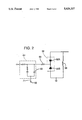
- FIG. 2 illustrates a portion of a local oscillator interface circuit used in the receiver of FIG. 1.
- the preferred embodiment of the present invention 10 includes an RF stage 12, an IF stage 14 and a baseband stage 16.
- the RF stage 12 includes an antenna 18 which may be fabricated into the wristband 20 of a wristwatch 22 in which the receiver 10 is mounted. (A suitable wristwatch enclosure is described in the Gaskill et al. patent).
- the antenna 18 provides RF signals to an antenna tuner stage 24.
- Antenna tuner stage 24 can be a varactor controlled notch filter which also performs limited impedance matching functions.
- a tuning voltage is applied to a tune voltage port 26 from a microprocessor based control system 27, such as is discussed in Gaskill et al. This voltage tunes a voltage-variable capacitor in tuner 24 which places the null of a notch filter at the image of the frequency to which the receiver is tuned. (This element of the invention can readily be omitted in alternative embodiments if image rejection is not a problem).
- the antenna tuner 24 also serves a limited impedance transformation function.
- the antenna 18 with which the receiver 10 is used is typically a very small loop and consequently has a very small impedance. Receiver performance and noise figure are optimized if this impedance is transformed up to more closely match the input impedance of the following RF amplifier stage 28.
- RF amplifier stage 28 is a low noise broadband amplifier tuned for maximum gain in the FM broadcast band (88-108 megahertz).
- the maximum gain of RF amplifier stage 28 is approximately 10 dB. Its actual gain is controlled by an AGC control circuit 30 discussed below. Since there is little in the way of preselector circuitry in or before the RF amplifier stage 28, the following receiver mixer stage 32 is provided with a wide band of amplified input signals.
- mixer stage 32 is configured in an image cancelling topology.
- Two individual mixers 34, 36 are driven with quadrature local oscillator signals on lines 38, 40 from a local oscillator 42.
- High side injection is generally used, so the local oscillator tunes the 98.7 to 118.7 megahertz range to yield a 10.7 megahertz intermediate frequency. (In some foreign countries, the adjoining frequencies are allocated to different services and it may be desirable to use low side injection instead).
- the local oscillator 42 is discussed in greater detail below.
- the output of the mixer 34 driven from local oscillator line 38 is delayed 90 degrees and is combined with the output of the mixer 36 that is driven from the delayed local oscillator line 40. The combination of these signals cancels any image response while reinforcing the desired signal response.
- Mixer 32 has a conversion gain at the desired signal frequency of approximately 7 dB.
- the output of mixer stage 32 is provided to an IF chain 14 comprised of two IF amplifiers 46, 48 and two ceramic band pass filters 50, 52.
- Filters 50, 52 are desirably of non-identical design so as to avoid co-location of spurious filter responses within the IF pass band.
- the filters are of chip construction and may be of the SFEC 10.7 series manufactured by Murata.
- IF amplifiers 46, 48 have gains of approximately 20 dB each and filters 50, 52 have about 6 dB each of loss.
- the IF amplifiers 46, 48 are gain controlled, as discussed below, to optimize signal-to-noise ratio.
- the output of IF chain 14 is provided to a synchronous, or coherent detector comprised of a mixer 54 injected with a 10.7 megahertz signal from a second local oscillator 58.
- the synchronous detection technique permits detection at a much lower signal level than would be possible if a limiter or discriminator stage was employed. Consequently, the IF stage gain can be lower than would normally be the case, thereby reducing the risk of oscillation caused by stray feedback.
- Synchronous detection also requires fewer and simpler off-chip components than alternative detection techniques and is simpler to adjust.
- the local oscillator 58 providing the 10.7 megahertz signal to the synchronous detector 54 is locked to the frequency of the IF by a feedback circuit 56.
- the 10.7 megahertz signal causes the mixer 54 to yield an output signal on line 62 that is proportional to the frequency of the signal modulating the 10.7 megahertz IF.
- the feedback circuit 56 causes the oscillator 58 to lock 90 degrees from the phase of the I.F. signal).
- This baseband frequency modulated signal is fed to a low pass filter 64 and then to a high gain baseband amplifier 66.
- Baseband amplifier 66 has a break point of about five kilohertz for discrimination against the left plus right FM stereo channel. This breakpoint also minimizes distortion caused by the main audio channel bleeding into the subcarrier channel.
- the high end rolloff breakpoint is at about 150 kilohertz.
- the output of the baseband amplifier 66 is provided to conventional decoder circuitry, as disclosed in the Gaskill et al. patent.
- a second synchronous detector is also driven by the IF chain 14 and provides an AGC signal for application to the RF and IF gain stages.
- This second synchronous detector again includes a mixer 68, this one driven from the 10.7 megahertz local oscillator 58 through a 90 degree phase shifter 60.
- the output of this mixer 68 is thus related to the amplitude of the IF signal and can be used to gain control preceding stages.
- AGC circuitry 30 employed in the preferred embodiment of the present invention is disclosed in pending allowed application Ser. No. 07/196,946 now U.S. Pat. No. 4,870,372 of Suter entitled "AGC Delay on an Integrated Circuit," the disclosure of which is incorporated herein by reference.
- An AGC loop filter 70 is a single RC stage with a break point at about one kilohertz. All other bypassing of AGC points is done with much higher break points so that the one pole is clearly dominant.
- each paging receiver is periodically energized for a short interval, such as 33 milliseconds, and tuned to a frequency on which paging signals are expected. If paging signals are not found, the receiver undertakes a scan of other broadcast frequencies.
- the local oscillator 42 includes a fractional-N synthesizer.
- this oscillator includes first and second programmable divider circuits 81, 82, a digital mixer 83, a loop filter 84, a voltage controlled oscillator 85, and a divide-by-four circuit 86, all connected in a servo loop arrangement.
- the first divider circuit 81 divides a signal applied to its input 87 by either 31 or 32, depending on data provided to a control input 88 by the control microprocessor 27.
- the second divider circuit 82 similarly divides the signal output from the first divider circuit by N, where N is again a datum provided to a control input 90 by the microprocessor 27.
- the twice-divided signal is provided on line 91 to a mixer 83 that mixes it with a 50 KHz reference clock signal. This mixer produces a difference term that represents the difference in phase between the signal on line 91 and the reference clock signal.
- phase difference If the phase difference is greater than 360 degrees, the difference term becomes a difference frequency.
- This difference term is filtered from the other mixer products by the loop filter 84 and is applied to an input of the voltage controlled oscillator 85.
- These servo loop components cooperate together in their operation so that the frequency output by this oscillator is maintained at 50N KHz.
- FIG. 2 shows the- connection between loop filter 84 and voltage controlled oscillator 85.
- the output voltage from the loop filter 84 appears across capacitor 93.
- Varactor network 92 which includes varactors 92A and 92B together with inductance 98 are the frequency determining elements of oscillator 85.
- the voltage across capacitor 93 is applied to varactors 92A and 92B through a decoupling resistor 99.
- the varactor network 92 controls the frequency of the oscillator 85 in response to the voltage on capacitor 93.
- the control microprocessor deenergizes these components after the charge on the storage capacitor 93 has stabilized. In the illustrated embodiment, this takes about 4 milliseconds. For the remainder of the 33 millisecond listening interval, the voltage controlled oscillator relies on the capacitor 93 to maintain the receiver on the desired frequency.
- the storage capacitor 93 begins to discharge during this second portion of the listening interval, causing the receiver to drift off frequency.
- an AFC signal is applied to terminal 95.
- This AFC signal is taken from the output of the first synchronous detector 54 (which produces an output signal related to the frequency of the IF signal), amplified by an amplifier 72, routed through a switch 74 and applied to the second varactor terminal.
- a corresponding compensation signal is generated by the drifting IF signal on the AFC line 71, returning the receiver to its original frequency.
- the AFC control loop not only tracks drift caused by discharge of the storage capacitor, but also corrects frequency errors caused by changes in supply voltage, ambient temperature, etc.
- Switch 74 is activated by the control microprocessor 27 to apply the AFC signal to the varactor at the same time the microprocessor shuts down the synthesizer. While the synthesizer is operative, the switch is in a second position in which it applies a reference voltage to the varactor. This reference voltage is selected to correspond to the signal generated on AFC line 71 when the received signal is properly centered in the IF passband.
- the tuning voltage applied across the varactor 92 spans a 4.5 volt range, from -2.25 volts to 2.25 volts, and is generated by a voltage doubler circuit from a nominal 2.25 volt receiver supply voltage.
- the nominal AFC voltage is approximately 200 millivolts below this supply voltage and can vary plus or minus 200 millivolts.
- the foregoing arrangement not only eliminates noise from the synthesizer; it also reduces battery power.
- the power consumption of the receiver circuitry drops about 20 to 25% percent when the synthesizer is shut down and frequency control is left to the AFC loop.
Abstract
Description
Claims (1)
Priority Applications (6)
| Application Number | Priority Date | Filing Date | Title |
|---|---|---|---|
| US07/388,228 US5029237A (en) | 1988-06-30 | 1989-08-01 | Radio receiver frequency control system |
| AU60665/90A AU6066590A (en) | 1989-08-01 | 1990-07-23 | Radio receiver frequency control system |
| EP19900911835 EP0485453A4 (en) | 1989-08-01 | 1990-07-23 | Radio receiver frequency control system |
| PCT/US1990/004140 WO1991002413A1 (en) | 1989-08-01 | 1990-07-23 | Radio receiver frequency control system |
| JP2511094A JPH05503192A (en) | 1989-08-01 | 1990-07-23 | Radio receiver frequency control system |
| CA002064895A CA2064895A1 (en) | 1989-08-01 | 1990-07-23 | Radio receiver frequency control system |
Applications Claiming Priority (2)
| Application Number | Priority Date | Filing Date | Title |
|---|---|---|---|
| US07/213,719 US4885802A (en) | 1988-06-30 | 1988-06-30 | Wristwatch receiver architecture |
| US07/388,228 US5029237A (en) | 1988-06-30 | 1989-08-01 | Radio receiver frequency control system |
Related Parent Applications (1)
| Application Number | Title | Priority Date | Filing Date |
|---|---|---|---|
| US07/213,719 Continuation-In-Part US4885802A (en) | 1988-06-30 | 1988-06-30 | Wristwatch receiver architecture |
Publications (1)
| Publication Number | Publication Date |
|---|---|
| US5029237A true US5029237A (en) | 1991-07-02 |
Family
ID=23533221
Family Applications (1)
| Application Number | Title | Priority Date | Filing Date |
|---|---|---|---|
| US07/388,228 Expired - Lifetime US5029237A (en) | 1988-06-30 | 1989-08-01 | Radio receiver frequency control system |
Country Status (6)
| Country | Link |
|---|---|
| US (1) | US5029237A (en) |
| EP (1) | EP0485453A4 (en) |
| JP (1) | JPH05503192A (en) |
| AU (1) | AU6066590A (en) |
| CA (1) | CA2064895A1 (en) |
| WO (1) | WO1991002413A1 (en) |
Cited By (11)
| Publication number | Priority date | Publication date | Assignee | Title |
|---|---|---|---|---|
| US5163160A (en) * | 1989-09-14 | 1992-11-10 | Alcatel Espace | Satellite transponder able to use same frequency scheme for transmitter and receiver local oscillator |
| US5329319A (en) * | 1991-02-20 | 1994-07-12 | Zenith Electronics Corporation | Stabilized frequency and phase locked loop with saw devices on common substrate |
| US5530929A (en) * | 1993-09-09 | 1996-06-25 | Ericsson Ge Mobile Communications Inc. | Homodyne receiver minimizing oscillator leakage |
| US5983088A (en) * | 1995-01-23 | 1999-11-09 | Rca Thomson Licensing Corporation | Wide frequency spectrum television tuner with single local oscillator |
| DE19946494A1 (en) * | 1999-09-28 | 2001-05-03 | Infineon Technologies Ag | Receiver for different frequency bands |
| US20020041340A1 (en) * | 2000-10-05 | 2002-04-11 | Alps Electric Co., Ltd. | TV signal receiving tuner capable of outputting oscillation signal having wide frequency band by means of single local oscillator |
| US20020049044A1 (en) * | 2000-10-19 | 2002-04-25 | Alcatel | Phase-linear wide band frequency conversion |
| US20020197972A1 (en) * | 2001-06-20 | 2002-12-26 | Motorola, Inc. | Image rejection mixer with switchable high or low side injection |
| US6640093B1 (en) * | 1909-06-29 | 2003-10-28 | Sony International (Europe) Gmbh | Broadcast receiver |
| US7751164B1 (en) | 2003-01-29 | 2010-07-06 | Marvell International Ltd. | Electrostatic discharge protection circuit |
| WO2012151191A1 (en) * | 2011-05-05 | 2012-11-08 | Telcordia Technologies | Directional notch filter for simultaneous transimt and receive of wideband signals |
Families Citing this family (2)
| Publication number | Priority date | Publication date | Assignee | Title |
|---|---|---|---|---|
| US5428820A (en) * | 1993-10-01 | 1995-06-27 | Motorola | Adaptive radio receiver controller method and apparatus |
| JP4089003B2 (en) * | 1998-04-01 | 2008-05-21 | ソニー株式会社 | Receiver and receiving method |
Citations (11)
| Publication number | Priority date | Publication date | Assignee | Title |
|---|---|---|---|---|
| US4365349A (en) * | 1980-02-01 | 1982-12-21 | Nippon Gakki Seizo Kabushiki Kaisha | Radio receiver having phase locked loop and automatic frequency control loop for stably maintaining local oscillator frequency of voltage-controlled local oscillator |
| US4384361A (en) * | 1979-09-29 | 1983-05-17 | Nippon Electric Co., Ltd. | Selective calling receiver |
| US4521918A (en) * | 1980-11-10 | 1985-06-04 | General Electric Company | Battery saving frequency synthesizer arrangement |
| US4590618A (en) * | 1984-03-13 | 1986-05-20 | Motorola, Inc. | Receiver having reference voltage stabilization circuitry |
| US4598288A (en) * | 1979-04-16 | 1986-07-01 | Codart, Inc. | Apparatus for controlling the reception of transmitted programs |
| US4631496A (en) * | 1981-04-06 | 1986-12-23 | Motorola, Inc. | Battery saving system for a frequency synthesizer |
| US4703520A (en) * | 1986-10-31 | 1987-10-27 | Motorola, Inc. | Radio transceiver having an adaptive reference oscillator |
| US4713808A (en) * | 1985-11-27 | 1987-12-15 | A T & E Corporation | Watch pager system and communication protocol |
| US4743857A (en) * | 1984-04-18 | 1988-05-10 | Telex Computer Products, Inc. | Digital/analog phase-locked oscillator |
| US4743864A (en) * | 1985-10-23 | 1988-05-10 | Hitachi, Ltd | Power saving intermittently operated phase locked loop |
| US4890094A (en) * | 1988-10-07 | 1989-12-26 | David Kopel | Wallet incorporating credit card alarm system |
Family Cites Families (2)
| Publication number | Priority date | Publication date | Assignee | Title |
|---|---|---|---|---|
| IT1223524B (en) * | 1987-12-18 | 1990-09-19 | Honeywell Bull Spa | SELF-CALIBRATING PHASE HOOK CIRCUIT |
| US4893094A (en) * | 1989-03-13 | 1990-01-09 | Motorola, Inc. | Frequency synthesizer with control of start-up battery saving operations |
-
1989
- 1989-08-01 US US07/388,228 patent/US5029237A/en not_active Expired - Lifetime
-
1990
- 1990-07-23 EP EP19900911835 patent/EP0485453A4/en not_active Withdrawn
- 1990-07-23 CA CA002064895A patent/CA2064895A1/en not_active Abandoned
- 1990-07-23 WO PCT/US1990/004140 patent/WO1991002413A1/en not_active Application Discontinuation
- 1990-07-23 JP JP2511094A patent/JPH05503192A/en active Pending
- 1990-07-23 AU AU60665/90A patent/AU6066590A/en not_active Abandoned
Patent Citations (11)
| Publication number | Priority date | Publication date | Assignee | Title |
|---|---|---|---|---|
| US4598288A (en) * | 1979-04-16 | 1986-07-01 | Codart, Inc. | Apparatus for controlling the reception of transmitted programs |
| US4384361A (en) * | 1979-09-29 | 1983-05-17 | Nippon Electric Co., Ltd. | Selective calling receiver |
| US4365349A (en) * | 1980-02-01 | 1982-12-21 | Nippon Gakki Seizo Kabushiki Kaisha | Radio receiver having phase locked loop and automatic frequency control loop for stably maintaining local oscillator frequency of voltage-controlled local oscillator |
| US4521918A (en) * | 1980-11-10 | 1985-06-04 | General Electric Company | Battery saving frequency synthesizer arrangement |
| US4631496A (en) * | 1981-04-06 | 1986-12-23 | Motorola, Inc. | Battery saving system for a frequency synthesizer |
| US4590618A (en) * | 1984-03-13 | 1986-05-20 | Motorola, Inc. | Receiver having reference voltage stabilization circuitry |
| US4743857A (en) * | 1984-04-18 | 1988-05-10 | Telex Computer Products, Inc. | Digital/analog phase-locked oscillator |
| US4743864A (en) * | 1985-10-23 | 1988-05-10 | Hitachi, Ltd | Power saving intermittently operated phase locked loop |
| US4713808A (en) * | 1985-11-27 | 1987-12-15 | A T & E Corporation | Watch pager system and communication protocol |
| US4703520A (en) * | 1986-10-31 | 1987-10-27 | Motorola, Inc. | Radio transceiver having an adaptive reference oscillator |
| US4890094A (en) * | 1988-10-07 | 1989-12-26 | David Kopel | Wallet incorporating credit card alarm system |
Cited By (15)
| Publication number | Priority date | Publication date | Assignee | Title |
|---|---|---|---|---|
| US6640093B1 (en) * | 1909-06-29 | 2003-10-28 | Sony International (Europe) Gmbh | Broadcast receiver |
| US5163160A (en) * | 1989-09-14 | 1992-11-10 | Alcatel Espace | Satellite transponder able to use same frequency scheme for transmitter and receiver local oscillator |
| US5329319A (en) * | 1991-02-20 | 1994-07-12 | Zenith Electronics Corporation | Stabilized frequency and phase locked loop with saw devices on common substrate |
| US5530929A (en) * | 1993-09-09 | 1996-06-25 | Ericsson Ge Mobile Communications Inc. | Homodyne receiver minimizing oscillator leakage |
| US5983088A (en) * | 1995-01-23 | 1999-11-09 | Rca Thomson Licensing Corporation | Wide frequency spectrum television tuner with single local oscillator |
| US6600912B1 (en) | 1999-09-28 | 2003-07-29 | Infineon Technologies Ag | Receiver for various frequency bands |
| DE19946494A1 (en) * | 1999-09-28 | 2001-05-03 | Infineon Technologies Ag | Receiver for different frequency bands |
| US20020041340A1 (en) * | 2000-10-05 | 2002-04-11 | Alps Electric Co., Ltd. | TV signal receiving tuner capable of outputting oscillation signal having wide frequency band by means of single local oscillator |
| US6842198B2 (en) * | 2000-10-05 | 2005-01-11 | Alps Electric Co., Ltd. | TV signal receiving tuner capable of outputting oscillation signal having wide frequency band by means of single local oscillator |
| US20020049044A1 (en) * | 2000-10-19 | 2002-04-25 | Alcatel | Phase-linear wide band frequency conversion |
| US20020197972A1 (en) * | 2001-06-20 | 2002-12-26 | Motorola, Inc. | Image rejection mixer with switchable high or low side injection |
| US6952572B2 (en) | 2001-06-20 | 2005-10-04 | Freescale Semiconductor, Inc. | Image rejection mixer with switchable high or low side injection |
| US7751164B1 (en) | 2003-01-29 | 2010-07-06 | Marvell International Ltd. | Electrostatic discharge protection circuit |
| WO2012151191A1 (en) * | 2011-05-05 | 2012-11-08 | Telcordia Technologies | Directional notch filter for simultaneous transimt and receive of wideband signals |
| US8942658B2 (en) | 2011-05-05 | 2015-01-27 | Telcordia Technologies, Inc. | Directional notch filter for simultaneous transmit and receive of wideband signals |
Also Published As
| Publication number | Publication date |
|---|---|
| EP0485453A4 (en) | 1992-09-30 |
| JPH05503192A (en) | 1993-05-27 |
| AU6066590A (en) | 1991-03-11 |
| EP0485453A1 (en) | 1992-05-20 |
| CA2064895A1 (en) | 1991-02-02 |
| WO1991002413A1 (en) | 1991-02-21 |
Similar Documents
| Publication | Publication Date | Title |
|---|---|---|
| US5029237A (en) | Radio receiver frequency control system | |
| EP0900479A1 (en) | Highly stable frequency synthesizer loop with feedforward | |
| JPS627728B2 (en) | ||
| US5243356A (en) | Antenna circuit and wrist radio instrument | |
| EP0456099B1 (en) | On channel agile FM demodulator | |
| US5603099A (en) | Transceiver for preventing the degradation of reception sensitivity and modulation accuracy of a transmitted signal when an external reference signal incorporates noise | |
| US4831339A (en) | Oscillator having low phase noise | |
| KR960000523B1 (en) | Receiver | |
| CA2118810C (en) | Radio having a combined pll and afc loop and method of operating the same | |
| US5789987A (en) | Low-noise frequency synthesizer | |
| US6198825B1 (en) | Wireless speaker circuit | |
| EP0519562B1 (en) | Phase-locked loop receiver | |
| JP2553219B2 (en) | RF modulator and video cassette recorder incorporating the same | |
| JPS5924191Y2 (en) | Synthesizer-receiver AFC circuit | |
| JPS627729B2 (en) | ||
| JP2000174652A (en) | Fm receiver | |
| JPS5947496B2 (en) | Receiving machine | |
| JP3053838B2 (en) | Video intermediate frequency circuit | |
| AU603216B2 (en) | Tweet elimination, or reduction, in superheterodyne receivers | |
| JPS6234177B2 (en) | ||
| JPS60223335A (en) | Turner of am/fm receiver | |
| JPH05176327A (en) | Tuner | |
| JPS6363136B2 (en) | ||
| WO1995010880A1 (en) | Adaptive bandwidth controlled frequency synthesizer | |
| JPH04245814A (en) | Fm transmission circuit |
Legal Events
| Date | Code | Title | Description |
|---|---|---|---|
| AS | Assignment |
Owner name: AT&E CORPORATION, ONE MARITIME PLAZA, SAN FRANCISC Free format text: ASSIGNMENT OF ASSIGNORS INTEREST.;ASSIGNOR:RAGAN, LAWRENCE H.;REEL/FRAME:005112/0758 Effective date: 19890731 |
|
| STCF | Information on status: patent grant |
Free format text: PATENTED CASE |
|
| AS | Assignment |
Owner name: SEIKO CORPORATION, JAPAN Free format text: ASSIGNMENT OF ASSIGNORS INTEREST.;ASSIGNOR:AT&E CORPORATION;REEL/FRAME:005996/0617 Effective date: 19911231 Owner name: SEIKO EPSON CORPORATION, JAPAN Free format text: ASSIGNMENT OF ASSIGNORS INTEREST.;ASSIGNOR:AT&E CORPORATION;REEL/FRAME:005996/0617 Effective date: 19911231 |
|
| FEPP | Fee payment procedure |
Free format text: PAT HLDR NO LONGER CLAIMS SMALL ENT STAT AS SMALL BUSINESS (ORIGINAL EVENT CODE: LSM2); ENTITY STATUS OF PATENT OWNER: LARGE ENTITY |
|
| FPAY | Fee payment |
Year of fee payment: 4 |
|
| FPAY | Fee payment |
Year of fee payment: 8 |
|
| FPAY | Fee payment |
Year of fee payment: 12 |
|
| AS | Assignment |
Owner name: SEIKO INSTRUMENTS INC., JAPAN Free format text: ASSIGNMENT OF ASSIGNORS INTEREST;ASSIGNORS:SEIKO CORPORATION;SEIKO EPSON CORPORATION;REEL/FRAME:018398/0844;SIGNING DATES FROM 20060621 TO 20060920 |
|
| AS | Assignment |
Owner name: SEIKO HOLDINGS CORPORATION, JAPAN Free format text: CHANGE OF NAME;ASSIGNOR:SEIKO CORPORATION;REEL/FRAME:021029/0634 Effective date: 20070701 Owner name: SEIKO INSTRUMENTS INC., JAPAN Free format text: ASSIGNMENT OF ASSIGNORS INTEREST;ASSIGNORS:SEIKO HOLDINGS CORPORATION;SEIKO EPSON CORPORATION;REEL/FRAME:021029/0649;SIGNING DATES FROM 20080423 TO 20080505 |
|
| FEPP | Fee payment procedure |
Free format text: PAYER NUMBER DE-ASSIGNED (ORIGINAL EVENT CODE: RMPN); ENTITY STATUS OF PATENT OWNER: LARGE ENTITY Free format text: PAYOR NUMBER ASSIGNED (ORIGINAL EVENT CODE: ASPN); ENTITY STATUS OF PATENT OWNER: LARGE ENTITY |
|
| AS | Assignment |
Owner name: PROTOCOL-IP.COM, L.L.C., DELAWARE Free format text: ASSIGNMENT OF ASSIGNORS INTEREST;ASSIGNOR:SEIKO INSTRUMENTS INC.;REEL/FRAME:022024/0063 Effective date: 20080201 |