US5013400A - Dry etch process for forming champagne profiles, and dry etch apparatus - Google Patents
Dry etch process for forming champagne profiles, and dry etch apparatus Download PDFInfo
- Publication number
- US5013400A US5013400A US07/472,327 US47232790A US5013400A US 5013400 A US5013400 A US 5013400A US 47232790 A US47232790 A US 47232790A US 5013400 A US5013400 A US 5013400A
- Authority
- US
- United States
- Prior art keywords
- plasma
- reaction vessel
- electrode
- preselected
- pressure
- Prior art date
- Legal status (The legal status is an assumption and is not a legal conclusion. Google has not performed a legal analysis and makes no representation as to the accuracy of the status listed.)
- Expired - Fee Related
Links
Images


Classifications
-
- H—ELECTRICITY
- H01—ELECTRIC ELEMENTS
- H01L—SEMICONDUCTOR DEVICES NOT COVERED BY CLASS H10
- H01L21/00—Processes or apparatus adapted for the manufacture or treatment of semiconductor or solid state devices or of parts thereof
- H01L21/70—Manufacture or treatment of devices consisting of a plurality of solid state components formed in or on a common substrate or of parts thereof; Manufacture of integrated circuit devices or of parts thereof
- H01L21/71—Manufacture of specific parts of devices defined in group H01L21/70
- H01L21/768—Applying interconnections to be used for carrying current between separate components within a device comprising conductors and dielectrics
- H01L21/76801—Applying interconnections to be used for carrying current between separate components within a device comprising conductors and dielectrics characterised by the formation and the after-treatment of the dielectrics, e.g. smoothing
- H01L21/76802—Applying interconnections to be used for carrying current between separate components within a device comprising conductors and dielectrics characterised by the formation and the after-treatment of the dielectrics, e.g. smoothing by forming openings in dielectrics
- H01L21/76804—Applying interconnections to be used for carrying current between separate components within a device comprising conductors and dielectrics characterised by the formation and the after-treatment of the dielectrics, e.g. smoothing by forming openings in dielectrics by forming tapered via holes
-
- H—ELECTRICITY
- H01—ELECTRIC ELEMENTS
- H01L—SEMICONDUCTOR DEVICES NOT COVERED BY CLASS H10
- H01L21/00—Processes or apparatus adapted for the manufacture or treatment of semiconductor or solid state devices or of parts thereof
- H01L21/02—Manufacture or treatment of semiconductor devices or of parts thereof
- H01L21/04—Manufacture or treatment of semiconductor devices or of parts thereof the devices having at least one potential-jump barrier or surface barrier, e.g. PN junction, depletion layer or carrier concentration layer
- H01L21/18—Manufacture or treatment of semiconductor devices or of parts thereof the devices having at least one potential-jump barrier or surface barrier, e.g. PN junction, depletion layer or carrier concentration layer the devices having semiconductor bodies comprising elements of Group IV of the Periodic System or AIIIBV compounds with or without impurities, e.g. doping materials
- H01L21/30—Treatment of semiconductor bodies using processes or apparatus not provided for in groups H01L21/20 - H01L21/26
- H01L21/31—Treatment of semiconductor bodies using processes or apparatus not provided for in groups H01L21/20 - H01L21/26 to form insulating layers thereon, e.g. for masking or by using photolithographic techniques; After treatment of these layers; Selection of materials for these layers
- H01L21/3105—After-treatment
- H01L21/311—Etching the insulating layers by chemical or physical means
- H01L21/31105—Etching inorganic layers
- H01L21/31111—Etching inorganic layers by chemical means
- H01L21/31116—Etching inorganic layers by chemical means by dry-etching
Definitions
- the instant invention is directed to the field of semiconductor device fabrication, and more particularly, to an improved dry etch process for forming champagne profiles in semiconductor oxide layers, and to dry etch apparatus.
- one or more plasmas are caused to interact with suitably prepared surfaces of semiconductor or other materials to form one or more intended microstructures thereon.
- the plasmas are controllably produced by two electrodes in a diode configuration
- the plasmas are controllably produced by three electrodes in a triode or other three-electrode configuration. Selected etches corresponding to the intended microstructures being fabricated are effected by varying the applied electrode powers and relative spacings, and by varying the gas chemistries and other plasma control parameters, in a manner well known to those skilled in the art.
- the electrode gap and gas chemistries were varied to first implement the isotropic step and then the anisotropic step.
- the gas chemistries for the isotropic etch were carbon tetrafluoride (CF 4 ) and oxygen (O 2 ), and the gas chemistries for the anisotropic etch implemented in the LAM-Research etcher and in the Applied Materials RIE hex etcher were a trifluoromethane (CHF 3 ) and oxygen (O 2 ) mixture.
- the three electrodes are powered in such a manner that the oxide layer first is etched isotropically by powering the side electrode while holding the wafer electrode at floating potential, and then etched anisotropically.
- the duty cycle which controls the ratio of the anisotropic to the isotropic etch, controls the oxide slope
- nitrogen trifluoride (NF 3 ) was the primary etchant reported.
- isotropic/anisotropic process mode different chemistries were used for the different tri-electrode RF power configurations, NF 3 for the isotropic etch and SF 6 /CHF 3 for the anisotropic etch.
- diode and triode reactors are known, such as the model "384"diode reactor commercially available from the instant assignee, and the Waferetch 606/616 triode reactor, commercially available from GCA Corporation.
- a novel process for fabricating champagne profiles in oxide layers previously applied to semiconductor or other wafers by a first plasma electrically and physically isolated from the wafer at a preselected comparatively-high pressure selected to provide a corresponding, comparatively-low mean free path to provide an isotropic etch, and thereafter by forming a second plasma electrically coupled and physically proximate the wafer at a preselected comparatively-low pressure selected to provide a corresponding, comparatively-high mean free path to provide an anisotropic etch.
- Both plasmas are formed in a single vessel.
- the champagne profiles fabricated thereby exhibit good critical dimension control, and reproduceability profile to profile, wafer to wafer and batch to batch, and when subsequently metallized, they allow to provide microcracking-free contacts and vias.
- novel dry etch apparatus in accord with another object of the present invention, includes a reaction vessel in which three electrodes including a grid are mounted in a triode configuration to provide a first plasma forming region between one of the electrodes and the grid and a second plasma forming region between the grid and the other of the electrodes.
- a pressure control system is coupled to the reaction vessel for selecting pressure in the reaction vessel from a range of pressures that includes 50 mTorr to 3000 mTorr.
- An RF source is controllably coupled to the electrodes that cooperates with the pressure control system to selectively provide a first plasma only in the first plasma forming region that is electrically and physically isolated from the wafer at a preselected comparatively-high pressure selected to provide a comparatively-low mean free path, a second plasma only in the second plasma forming region that is physically proximate to and electrically coupled with the wafer at a preselected comparatively-low pressure selected to provide a comparatively-high mean free path, and a first and second plasma in the first and in the second plasma forming regions respectively.
- Selected reactant gases are introduced via a conduit coupled to one of the electrodes.
- Various temperature controllers are coupled to the electrodes, to the reaction vessel and to the region of the wafer electrode proximate the wafer for controlling the temperatures thereof.
- FIG. 1 is a drawing of a SEM picture illustrating an exemplary champagne profile of the type provided by the instant invention
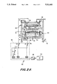
- FIG. 2 illustrates in FIG. 2A thereof a partially sectional and partially schematic view and illustrates in FIG. 2B thereof a partially pictorial and partially schematic view of the novel dry etch apparatus in accord with the present invention
- FIG. 3 is a block diagram illustrating the novel process for forming champagne profiles in accord with the present invention.
- FIG. 4 shows in FIG. 4A and FIG. 4B thereof sectional views of the dry etch apparatus useful in explaining the process for forming champagne profiles in accord with the present invention.
- FIG. 1 generally designated at 10 is a drawing of a SEM picture illustrating an exemplary champagne profile of the type provided by the instant invention.
- the profile 10 is formed in a manner to be described in an oxide layer generally designated 12, such as BPSG, previously applied to a semiconductor wafer or other substrate generally designated 14, at one or more predetermined locations thereof specified by a mask layer generally designated 16, such as photoresist, previously applied to the oxide layer 12.
- the champagne profile 10 includes a first curvilinear portion 18 isotropically etched in the oxide 12 by a first downstream plasma to be described, and a linear portion 20 anisotropically etched in the oxide 12 subjacent the portion 18 thereof by a second RIE plasma to be described.
- the etched profile 10 as constituted by the isotropically etched portion 18 and by the anisotropically etched portion 20, has been found to exhibit good critical dimension control and repeatability profile to profile, wafer to wafer and batch to batch, and when subsequently metallized, has been found to allow microcracking-free contacts and vias to be provided.
- the dry etch apparatus 30 includes a reaction vessel 32 into which an upper electrode 34, a grid 36, and a lower electrode 38 are mounted in spaced-apart relation in a triode configuration.
- a diffuser 40 is mounted between the grid 36 and the upper electrode 34. Reactant gases, supplied by a reactant gas injection tube 42, are injected, through apertures, not shown, provided therefor in the upper electrode 34, into the reaction vessel 32, and are diffused by the diffuser 40 as schematically illustrated by arrows 44.
- the upper electrode 34 has apertures generally designated 46 to allow the circulation of a heat transport fluid, such as water, thereinthrough to control the temperature of the upper electrode.
- a heat transport fluid such as water
- the vessel 32 is provided with bores into which resistive heating elements 48 are inserted to control the temperature of the reaction vessel.
- a clamp ring 50 cooperates with the lower electrode 38 to releasably hold a wafer 52 therebetween.
- the lower electrode 38 has apertures generally designated 54 confronting the wafer 52 to allow the circulation of a heat transport fluid, such as helium (He), thereinthrough to control the temperature of the wafer underside to both increase the rate of the isotropic oxide etch to be described and to minimize photoresist reticulation during the anisotropic oxide etch to be described.
- a heat transport fluid such as helium (He)
- the lower electrode 38 has apertures generally designated 56 to allow the circulation of a heat transport fluid, such as water, thereinthrough to control the temperature thereof.
- a heat transport fluid such as water
- a Z-actuator is coupled to the lower electrode 38 for moving it towards and away from the upper electrode 34, as schematically illustrated by an arrow 58, to control the dimension of the gap therebetween.
- An optical window generally designated 60 is provided through the vessel 32 to allow for optical emission end point determination of etch depth in a manner well known to those skilled in the art.
- An automatic matching network illustrated by a dashed box 62 is electrically connected to the upper electrode 34 and to the lower electrode 38 for controllably coupling RF power thereto.
- the grid electrode 36 is electrically grounded.
- a radio frequency power source 64 is coupled via a bi-directional coupling 66 to the automatic matching network 62.
- the output of the bi-directional coupling 66 is coupled to ground via a variable capacitor marked "C1", and is applied through an inductor marked "L1" both to the lower electrode 38, through a circuit leg having a variable capacitor marked "C2" in series therewith, and to the upper electrode 34, through a circuit leg having a variable capacitor marked "C3" in series therewith.
- Motors respectively marked “M1", “M2” and “M3” control the capacitance of the variable capacitors “C1”, “C2” and “C3” to selectively couple power to the upper and lower electrodes 34, 38 to selectively form a plasma only between the upper electrode 34 and the grid 36, a plasma only between the grid 36 and the lower electrode 38, and plasmas between the upper electrode and grid as well as between the grid and the lower electrode.
- annular plenum generally designated 68 is provided therebetween.
- a portal generally designated 70 is provided through the vessel 32 in communication with the plenum 68 to exhaust injected reactant gases, as illustrated by arrows 74, and to allow selected internal chamber pressurization to be established and maintained.
- the pressure control system 80 includes a pressure controller 82, that preferably includes feedback from a pressure manometer, not shown, positioned in the reaction vessel, responsive to a chamber setpoint pressure selected from a range of pressures that includes 50 mTorr to 3000 mTorr to control a motor 86.
- the motor 86 in turn controls the aperture size of a variable orifice throttle valve 88 connected between the portal 70 of the vessel 32 and a vacuum pump 90 along dual conduits 92, 94.
- the motor 86 selects a particular aperture size for the variable orifice throttle valve 88, the particular size of which in turn enables the pump 90 to induce the corresponding setpoint pressure in the vessel 32 selected from the range of pressures that includes 50 mTorr to 3000 mTorr.
- FIG. 3 generally designated at 100 is a block diagram illustrating the novel process for forming champagne profiles in accord with the present invention.
- the process is implemented on the dry etch apparatus described above in connection with the description of FIG. 2, it could as well be practiced on any other suitable dry etch apparatus without departing from the inventive concept.
- 125 mm wafers were etched, but other wafer sizes including 100 mm to 200 mm wafers could be employed as well without departing from the inventive concept.
- a substrate such as a wafer to be etched is mounted on the lower electrode 38 (FIG. 2A) and held in position by the clamp ring 50 (FIG. 2A).
- first reactant gases preferably CF 4 and O 2 are injected, preferably at 200 and 20 sccm, into the reaction chamber 32 (FIG. 2A) via the conduit 42 and the pressure in the chamber 32 (FIG. 2A) is set to a preselected first comparatively-high pressure by the pressure controller, controlled motor and throttle valve 82, 86, 88 (FIG. 2B).
- the range of flow rates for the CF 4 can be varied over the range including 150-500 sccm, and the flow rates for the O 2 can be varied over the ranges including 10 to 100 sccm.
- the first reactant gases CF 4 and O 2 are non-toxic and readily commercially available, and the preselected first comparatively-high pressure is preferably selected to be about 2200 mTorr.
- the preselected first comparatively-high pressure can be varied within the range that includes 1500 mTorr to 2500 mTorr, and good reliability, microcracking-free contacts and vias are still obtained when subsequently metallized. It is important that the preselected first comparatively-high pressure be selected to be greater than about 1000 mTorr, or such results cannot be obtained.
- a predetermined time is allowed to pass so that the first reactant gases and chamber first pressure stabilizes. This time typically is 10 seconds.
- the automatic matching network 62 couples radio frequency power only to the upper electrode 34 but not to the lower electrode, with the grid electrically grounded.
- 800 watts of radio frequency power at 13.56 MHz is applied thereby.
- the coupled radio frequency power induces a plasma generally designated 110 in FIG. 4A between the grid 36 and the upper electrode 34 only in the first plasma forming region of the vessel 32.
- the plasma 110 that includes charged and neutral species, is physically isolated from the wafer 52, and is electrically isolated therefrom by the grounded grid 36.
- Ions and other charged species are substantially contained in the first plasma forming region between the top electrode 34 and the grid 36 by the electrical isolation provided by the grounded grid and by the absence of any accelerating potential field emanating from the lower grid, thereby minimizing their contribution towards etching the wafer surface.
- the preselected first comparatively-high pressure, preferably 2200 mTorr, and corresponding comparatively-low mean free path between the charged and neutral species of the first plasma maximizes the etching by the neutral species, and further minimizes the etching by the charged species.
- their comparatively-low mean free path is believed to deplete their energy, by collisional processes, thereby further reducing the ability of any charged species that do migrate through the grid to substantially etch the wafer.
- these neutral species of the plasma 108 are then allowed to isotropically etch the wafer for a predetermined time until the curvilinear portion 18 (FIG. 1) has been etched in the oxide, typically for 2.5 minutes in the preferred embodiment.
- the isotropic etch proceeds at the rate of about 2000 ⁇ per minute.
- the reactant gases are evacuated from the chamber 32 (FIG. 2A) by the pump 90 (FIG. 2B), and the radio frequency source 62 (FIG. 2A) is turned off.
- second reactant gases preferably trifluoromethane (CHF 3 ) and perfluoroethane (C 2 F 6 ) are injected into the vessel 32 (FIG. 2A) preferably at 114 sccm and 38 sccm, respectively, via the conduit 42 (FIG. 2A), and a preselected second comparatively-low setpoint pressure, preferably 130 mTorr, is established in the vessel 32 via the pressure controller, motor, and variable orifice valve 82, 86, and 88 (FIG. 2B).
- CHF 3 trifluoromethane
- C 2 F 6 perfluoroethane
- the range of flow rates for the CHF 3 can be varied over the range including 70 to 200 sccm, and the range of flow rates for the C 2 F 6 can be varied over the range including 30 to 110 sccm.
- the preselected second comparatively-low pressure can be varied within the range that includes 100-400 mTorr, and good reliability, microcracking-free contacts and vias are still obtained when the champagne profiles are subsequently metallized.
- a predetermined time typically 15 seconds, is allowed to lapse to allow the second reactant gases and chamber second pressure to stabilize.
- radio frequency power is coupled entirely to the lower electrode 38 but not to the top electrode (FIG.2A), preferably 500 watts at 13.56 MHz, with the grid grounded, forming a second plasma having charged and neutral species only in the second plasma forming region between the ground grid 36 and the lower electrode 38 that is generally designated at 124 in FIG. 4B.
- the plasma 124 is physically adjacent and electrically in contact with the surface of the the wafer 52.
- the power coupled to the lower electrode causes an electronic field to emanate therefrom that acts to proximity focus and accelerate the charged species theretoward in generally-straight trajectories. Other focusing techniques can be employed as well without departing from the inventive concept.
- the preselected second comparatively-low pressure preferably 130 mTorr, and corresponding, comparatively-high mean free path between the neutral and charged species is believed to maximize the etching by the charged species, by allowing them to be accelerated towards the lower electrode and to contact the prepared surface of the wafer with reduced collisional interference.
- the preselected second pressure can be selected from the range of pressures that includes 100 to 400 mTorr, and good reliability, microcracking-free contacts and vias are still obtained when subsequently metallized.
- the plasma ions and other charged species proximity focused by the electronic field emanating from the lower electrode 38 as they are accelerated towards the wafer are allowed to anisotropically etch the oxide 12 forming thereby the linear portion 20 (FIG. 1) of the champagne profile.
- the anisotropic etch proceeds at the rate from about 8,000 to 10,000 ⁇ per minute.
- the second plasma is allowed to anisotropically etch the oxide of the wafer until a suitable depth has been achieved as detected by the optical emission end point detector.
- the second reactant gases are pumped out of the chamber and the radio frequency power is turned off.
Abstract
Description
______________________________________
                  STEP 1  STEP 2
______________________________________
CF.sub.4     (sccm)     200
O.sub.2      (sccm)     20
CHF.sub.3    (sccm)               114
C.sub.2 F.sub.6
             (sccm)               38
Pressure     (mTorr)    2200      130
RF Power     (Watts)    800       500
Power Split  (% RIE)    0         100
DC Bias Upper
             (Volts)    -176
DC Bias Lower
             (Volts)              800
Etch Time    (mm:ss)    2:00      1:00
He Pressure  (Torr)     4.0       12.0
Temperature  (C)        40        40
Wafer size   (mm)       125       125
______________________________________
Claims (33)
Priority Applications (2)
| Application Number | Priority Date | Filing Date | Title |
|---|---|---|---|
| US07/472,327 US5013400A (en) | 1990-01-30 | 1990-01-30 | Dry etch process for forming champagne profiles, and dry etch apparatus |
| JP3216682A JP2816374B2 (en) | 1990-01-30 | 1991-01-29 | Dry etching method and apparatus for champagne contour |
Applications Claiming Priority (1)
| Application Number | Priority Date | Filing Date | Title |
|---|---|---|---|
| US07/472,327 US5013400A (en) | 1990-01-30 | 1990-01-30 | Dry etch process for forming champagne profiles, and dry etch apparatus |
Publications (1)
| Publication Number | Publication Date |
|---|---|
| US5013400A true US5013400A (en) | 1991-05-07 |
Family
ID=23875069
Family Applications (1)
| Application Number | Title | Priority Date | Filing Date |
|---|---|---|---|
| US07/472,327 Expired - Fee Related US5013400A (en) | 1990-01-30 | 1990-01-30 | Dry etch process for forming champagne profiles, and dry etch apparatus |
Country Status (2)
| Country | Link |
|---|---|
| US (1) | US5013400A (en) |
| JP (1) | JP2816374B2 (en) |
Cited By (55)
| Publication number | Priority date | Publication date | Assignee | Title |
|---|---|---|---|---|
| US5248371A (en) * | 1992-08-13 | 1993-09-28 | General Signal Corporation | Hollow-anode glow discharge apparatus |
| US5292554A (en) * | 1992-11-12 | 1994-03-08 | Applied Materials, Inc. | Deposition apparatus using a perforated pumping plate |
| US5304248A (en) * | 1990-12-05 | 1994-04-19 | Applied Materials, Inc. | Passive shield for CVD wafer processing which provides frontside edge exclusion and prevents backside depositions |
| US5308431A (en) * | 1986-04-18 | 1994-05-03 | General Signal Corporation | System providing multiple processing of substrates |
| US5328722A (en) * | 1992-11-06 | 1994-07-12 | Applied Materials, Inc. | Metal chemical vapor deposition process using a shadow ring |
| US5344542A (en) * | 1986-04-18 | 1994-09-06 | General Signal Corporation | Multiple-processing and contamination-free plasma etching system |
| US5362358A (en) * | 1992-05-14 | 1994-11-08 | Nec Corporation | Dry etching apparatus and method of forming a via hole in an interlayer insulator using same |
| US5391252A (en) * | 1992-12-08 | 1995-02-21 | Hughes Aircraft Company | Plasma pressure control assembly |
| US5420068A (en) * | 1991-09-27 | 1995-05-30 | Nec Corporation | Semiconductor integrated circuit and a method for manufacturing a fully planar multilayer wiring structure |
| US5445709A (en) * | 1992-11-19 | 1995-08-29 | Hitachi, Ltd. | Anisotropic etching method and apparatus |
| EP0670590A2 (en) * | 1994-02-28 | 1995-09-06 | Applied Materials, Inc. | High pressure plasma treatment method and apparatus |
| US5534110A (en) * | 1993-07-30 | 1996-07-09 | Lam Research Corporation | Shadow clamp |
| US5597438A (en) * | 1995-09-14 | 1997-01-28 | Siemens Aktiengesellschaft | Etch chamber having three independently controlled electrodes |
| US5683540A (en) * | 1995-06-26 | 1997-11-04 | Boeing North American, Inc. | Method and system for enhancing the surface of a material for cleaning, material removal or as preparation for adhesive bonding or etching |
| US5695566A (en) * | 1995-05-24 | 1997-12-09 | Matsushita Electric Industrial Co.,Ltd. | Apparatus and method for plasma-processing |
| US5798904A (en) * | 1996-06-28 | 1998-08-25 | Lam Research Corporation | High power electrostatic chuck contact |
| US5805408A (en) * | 1995-12-22 | 1998-09-08 | Lam Research Corporation | Electrostatic clamp with lip seal for clamping substrates |
| US5820723A (en) * | 1996-06-05 | 1998-10-13 | Lam Research Corporation | Universal vacuum chamber including equipment modules such as a plasma generating source, vacuum pumping arrangement and/or cantilevered substrate support |
| US5838529A (en) * | 1995-12-22 | 1998-11-17 | Lam Research Corporation | Low voltage electrostatic clamp for substrates such as dielectric substrates |
| US5891807A (en) * | 1997-09-25 | 1999-04-06 | Siemens Aktiengesellschaft | Formation of a bottle shaped trench |
| US5940730A (en) * | 1995-12-29 | 1999-08-17 | Hyundai Electronics Industries Co., Ltd. | Method of forming a contact hole of a semiconductor device |
| US5948704A (en) * | 1996-06-05 | 1999-09-07 | Lam Research Corporation | High flow vacuum chamber including equipment modules such as a plasma generating source, vacuum pumping arrangement and/or cantilevered substrate support |
| US5990000A (en) * | 1997-02-20 | 1999-11-23 | Applied Materials, Inc. | Method and apparatus for improving gap-fill capability using chemical and physical etchbacks |
| US6008132A (en) * | 1995-10-26 | 1999-12-28 | Yamaha Corporation | Dry etching suppressing formation of notch |
| US6030902A (en) * | 1996-02-16 | 2000-02-29 | Micron Technology Inc | Apparatus and method for improving uniformity in batch processing of semiconductor wafers |
| US6103055A (en) * | 1986-04-18 | 2000-08-15 | Applied Materials, Inc. | System for processing substrates |
| US6117786A (en) * | 1998-05-05 | 2000-09-12 | Lam Research Corporation | Method for etching silicon dioxide using fluorocarbon gas chemistry |
| WO2000061384A1 (en) * | 1999-04-12 | 2000-10-19 | Matrix Integrated Systems, Inc. | Remote plasma generator |
| US6136712A (en) * | 1998-09-30 | 2000-10-24 | Lam Research Corporation | Method and apparatus for improving accuracy of plasma etching process |
| US6190233B1 (en) | 1997-02-20 | 2001-02-20 | Applied Materials, Inc. | Method and apparatus for improving gap-fill capability using chemical and physical etchbacks |
| US6228278B1 (en) | 1998-09-30 | 2001-05-08 | Lam Research Corporation | Methods and apparatus for determining an etch endpoint in a plasma processing system |
| US6245662B1 (en) * | 1998-07-23 | 2001-06-12 | Applied Materials, Inc. | Method of producing an interconnect structure for an integrated circuit |
| US6297163B1 (en) | 1998-09-30 | 2001-10-02 | Lam Research Corporation | Method of plasma etching dielectric materials |
| US6379466B1 (en) * | 1992-01-17 | 2002-04-30 | Applied Materials, Inc. | Temperature controlled gas distribution plate |
| US20030024902A1 (en) * | 2001-03-30 | 2003-02-06 | Li Si Yi | Method of plasma etching low-k dielectric materials |
| US20030066483A1 (en) * | 2001-10-05 | 2003-04-10 | Samsung Electronics Co., Inc. | Atomic layer deposition apparatus and method for operating the same |
| US6617257B2 (en) | 2001-03-30 | 2003-09-09 | Lam Research Corporation | Method of plasma etching organic antireflective coating |
| US6630407B2 (en) | 2001-03-30 | 2003-10-07 | Lam Research Corporation | Plasma etching of organic antireflective coating |
| US20030221616A1 (en) * | 2002-05-28 | 2003-12-04 | Micron Technology, Inc. | Magnetically-actuatable throttle valve |
| US20030232504A1 (en) * | 2002-06-14 | 2003-12-18 | Aaron Eppler | Process for etching dielectric films with improved resist and/or etch profile characteristics |
| US20040037971A1 (en) * | 2000-04-27 | 2004-02-26 | Toru Otsubo | Plasma processing apparatus and processing method |
| US6746961B2 (en) | 2001-06-19 | 2004-06-08 | Lam Research Corporation | Plasma etching of dielectric layer with etch profile control |
| US6771482B2 (en) | 2001-07-30 | 2004-08-03 | Unaxis Usa Inc. | Perimeter seal for backside cooling of substrates |
| US20040171260A1 (en) * | 2002-06-14 | 2004-09-02 | Lam Research Corporation | Line edge roughness control |
| US6833079B1 (en) * | 2000-02-17 | 2004-12-21 | Applied Materials Inc. | Method of etching a shaped cavity |
| US20060075966A1 (en) * | 2002-01-26 | 2006-04-13 | Applied Materials, Inc. | Apparatus and method for plasma assisted deposition |
| US20070065597A1 (en) * | 2005-09-15 | 2007-03-22 | Asm Japan K.K. | Plasma CVD film formation apparatus provided with mask |
| US20080057724A1 (en) * | 2006-08-31 | 2008-03-06 | Mark Kiehlbauch | Selective etch chemistries for forming high aspect ratio features and associated structures |
| US20090236311A1 (en) * | 2006-10-30 | 2009-09-24 | Fhr Anlagenbau Gmbh | Method and Apparatus for Structuring Components Made of a Material Composed of Silicon Oxide |
| US20100089533A1 (en) * | 2007-08-16 | 2010-04-15 | Ulvac, Inc. | Ashing apparatus |
| US20120083130A1 (en) * | 2010-10-05 | 2012-04-05 | Skyworks Solutions, Inc. | Apparatus and methods for shielding a plasma etcher electrode |
| US20140034239A1 (en) * | 2008-07-23 | 2014-02-06 | Applied Materials, Inc. | Differential counter electrode tuning in a plasma reactor with an rf-driven workpiece support electrode |
| US20140190411A1 (en) * | 2001-03-02 | 2014-07-10 | Applied Materials, Inc. | Lid assembly for a processing system to facilitate sequential deposition techniques |
| US9711364B2 (en) | 2010-10-05 | 2017-07-18 | Skyworks Solutions, Inc. | Methods for etching through-wafer vias in a wafer |
| US9920425B2 (en) * | 2014-08-13 | 2018-03-20 | Toshiba Memory Corporation | Semiconductor manufacturing apparatus and manufacturing method of semiconductor device |
Families Citing this family (1)
| Publication number | Priority date | Publication date | Assignee | Title |
|---|---|---|---|---|
| US8802545B2 (en) * | 2011-03-14 | 2014-08-12 | Plasma-Therm Llc | Method and apparatus for plasma dicing a semi-conductor wafer |
Citations (2)
| Publication number | Priority date | Publication date | Assignee | Title |
|---|---|---|---|---|
| US4776918A (en) * | 1986-10-20 | 1988-10-11 | Hitachi, Ltd. | Plasma processing apparatus |
| US4889588A (en) * | 1989-05-01 | 1989-12-26 | Tegal Corporation | Plasma etch isotropy control |
Family Cites Families (6)
| Publication number | Priority date | Publication date | Assignee | Title |
|---|---|---|---|---|
| JPS5744749A (en) * | 1980-08-27 | 1982-03-13 | Honda Motor Co Ltd | Controlling device of secondary air in suction air sistem of internal combustion engine |
| JPS60105236A (en) * | 1983-11-14 | 1985-06-10 | Toshiba Corp | Manufacture of semiconductor device |
| JP2515731B2 (en) * | 1985-10-25 | 1996-07-10 | 株式会社日立製作所 | Thin film forming apparatus and thin film forming method |
| JPS63126247A (en) * | 1986-11-17 | 1988-05-30 | Hitachi Ltd | Manufacture of semiconductor integrated circuit device |
| JPH01268886A (en) * | 1988-04-18 | 1989-10-26 | Fujitsu Ltd | Plasma dry etching method |
| JPH0215002A (en) * | 1988-07-01 | 1990-01-18 | Takeda Chem Ind Ltd | Carrier for agricultural chemical composed of crushed silica sand |
-
1990
- 1990-01-30 US US07/472,327 patent/US5013400A/en not_active Expired - Fee Related
-
1991
- 1991-01-29 JP JP3216682A patent/JP2816374B2/en not_active Expired - Lifetime
Patent Citations (2)
| Publication number | Priority date | Publication date | Assignee | Title |
|---|---|---|---|---|
| US4776918A (en) * | 1986-10-20 | 1988-10-11 | Hitachi, Ltd. | Plasma processing apparatus |
| US4889588A (en) * | 1989-05-01 | 1989-12-26 | Tegal Corporation | Plasma etch isotropy control |
Non-Patent Citations (12)
| Title |
|---|
| "Contact Hole and Via Profiling by High Rate Isotropic and Anisotropic Etching of Oxides", V. Grewal et al., Jun. 15-16, 1987 V-MIC Conf. 1987 IEEE. |
| "Isotropic Plasma Etching of Doped and Undoped Silicon Dioxide for Contact Holes and Vias", W. G. M. van den Hoek, et al., J. Vac. Sci. Technol. A 7(3), May/Jun. 1989, pp. 670-675. |
| "Silicon Dioxide Profile Control for Contacts and Vias", Leslie Giffen et al., Solid State Technology, Apr. 1989. |
| Contact Hole and Via Profiling by High Rate Isotropic and Anisotropic Etching of Oxides , V. Grewal et al., Jun. 15 16, 1987 V MIC Conf. 1987 IEEE. * |
| GCA Waferetch Application Note, Flexibility of Process Control with a Triode Etcher, E. Bogle Rohwer, et al., 1987 GCA Corporation, Plasma Systems Division. * |
| GCA Waferetch Application Note, Flexibility of Process Control with a Triode Etcher, E. Bogle-Rohwer, et al., 1987 GCA Corporation, Plasma Systems Division. |
| Isotropic Plasma Etching of Doped and Undoped Silicon Dioxide for Contact Holes and Vias W. G. M. van den Hoek, et al., J. Vac. Sci. Technol. A 7(3), May/Jun. 1989, pp. 670 675. * |
| Silicon Dioxide Profile Control for Contacts and Vias , Leslie Giffen et al., Solid State Technology, Apr. 1989. * |
| Waferetch ® Application Note, GCA Waferetch 606/616 Triode Etch Systems, data sheet, 1987 GCA Corporation, Plasma Systems Division. |
| Waferetch Application Note, Etching of Aluminum and Aluminum Silicon 1986 GCA Corporation, Plasma Systems Division. * |
| Waferetch Application Note, GCA Waferetch 606/616 Triode Etch Systems, data sheet, 1987 GCA Corporation, Plasma Systems Division. * |
| Waferetch® Application Note, Etching of Aluminum and Aluminum-Silicon 1986 GCA Corporation, Plasma Systems Division. |
Cited By (86)
| Publication number | Priority date | Publication date | Assignee | Title |
|---|---|---|---|---|
| US5308431A (en) * | 1986-04-18 | 1994-05-03 | General Signal Corporation | System providing multiple processing of substrates |
| US5344542A (en) * | 1986-04-18 | 1994-09-06 | General Signal Corporation | Multiple-processing and contamination-free plasma etching system |
| US6103055A (en) * | 1986-04-18 | 2000-08-15 | Applied Materials, Inc. | System for processing substrates |
| US5304248A (en) * | 1990-12-05 | 1994-04-19 | Applied Materials, Inc. | Passive shield for CVD wafer processing which provides frontside edge exclusion and prevents backside depositions |
| US5851299A (en) * | 1990-12-05 | 1998-12-22 | Applied Materials, Inc. | Passive shield for CVD wafer processing which provides frontside edge exclusion and prevents backside depositions |
| US5420068A (en) * | 1991-09-27 | 1995-05-30 | Nec Corporation | Semiconductor integrated circuit and a method for manufacturing a fully planar multilayer wiring structure |
| US6379466B1 (en) * | 1992-01-17 | 2002-04-30 | Applied Materials, Inc. | Temperature controlled gas distribution plate |
| US5362358A (en) * | 1992-05-14 | 1994-11-08 | Nec Corporation | Dry etching apparatus and method of forming a via hole in an interlayer insulator using same |
| US5441595A (en) * | 1992-05-14 | 1995-08-15 | Nec Corporation | Dry etching apparatus and method of forming a via hole in an interlayer insulator using same |
| US5248371A (en) * | 1992-08-13 | 1993-09-28 | General Signal Corporation | Hollow-anode glow discharge apparatus |
| US5328722A (en) * | 1992-11-06 | 1994-07-12 | Applied Materials, Inc. | Metal chemical vapor deposition process using a shadow ring |
| US5292554A (en) * | 1992-11-12 | 1994-03-08 | Applied Materials, Inc. | Deposition apparatus using a perforated pumping plate |
| US5445709A (en) * | 1992-11-19 | 1995-08-29 | Hitachi, Ltd. | Anisotropic etching method and apparatus |
| US5766498A (en) * | 1992-11-19 | 1998-06-16 | Hitachi, Ltd. | Anisotropic etching method and apparatus |
| US5391252A (en) * | 1992-12-08 | 1995-02-21 | Hughes Aircraft Company | Plasma pressure control assembly |
| US5656122A (en) * | 1993-07-30 | 1997-08-12 | Lam Research Corporation | Shadow clamp |
| US5534110A (en) * | 1993-07-30 | 1996-07-09 | Lam Research Corporation | Shadow clamp |
| EP0670590A3 (en) * | 1994-02-28 | 1997-08-20 | Applied Materials Inc | High pressure plasma treatment method and apparatus. |
| EP0670590A2 (en) * | 1994-02-28 | 1995-09-06 | Applied Materials, Inc. | High pressure plasma treatment method and apparatus |
| US5695566A (en) * | 1995-05-24 | 1997-12-09 | Matsushita Electric Industrial Co.,Ltd. | Apparatus and method for plasma-processing |
| US5683540A (en) * | 1995-06-26 | 1997-11-04 | Boeing North American, Inc. | Method and system for enhancing the surface of a material for cleaning, material removal or as preparation for adhesive bonding or etching |
| US5597438A (en) * | 1995-09-14 | 1997-01-28 | Siemens Aktiengesellschaft | Etch chamber having three independently controlled electrodes |
| US6008132A (en) * | 1995-10-26 | 1999-12-28 | Yamaha Corporation | Dry etching suppressing formation of notch |
| US5838529A (en) * | 1995-12-22 | 1998-11-17 | Lam Research Corporation | Low voltage electrostatic clamp for substrates such as dielectric substrates |
| US5805408A (en) * | 1995-12-22 | 1998-09-08 | Lam Research Corporation | Electrostatic clamp with lip seal for clamping substrates |
| US5940730A (en) * | 1995-12-29 | 1999-08-17 | Hyundai Electronics Industries Co., Ltd. | Method of forming a contact hole of a semiconductor device |
| DE19654560B4 (en) * | 1995-12-29 | 2005-11-10 | Hyundai Electronics Industries Co., Ltd., Ichon | A method of forming a contact hole in a semiconductor device |
| US6315859B1 (en) | 1996-02-16 | 2001-11-13 | Micron Technology, Inc. | Apparatus and method for improving uniformity in batch processing of semiconductor wafers |
| US6607987B2 (en) * | 1996-02-16 | 2003-08-19 | Micron Technology, Inc. | Method for improving uniformity in batch processing of semiconductor wafers |
| US6030902A (en) * | 1996-02-16 | 2000-02-29 | Micron Technology Inc | Apparatus and method for improving uniformity in batch processing of semiconductor wafers |
| US5948704A (en) * | 1996-06-05 | 1999-09-07 | Lam Research Corporation | High flow vacuum chamber including equipment modules such as a plasma generating source, vacuum pumping arrangement and/or cantilevered substrate support |
| US5820723A (en) * | 1996-06-05 | 1998-10-13 | Lam Research Corporation | Universal vacuum chamber including equipment modules such as a plasma generating source, vacuum pumping arrangement and/or cantilevered substrate support |
| US5798904A (en) * | 1996-06-28 | 1998-08-25 | Lam Research Corporation | High power electrostatic chuck contact |
| US6190233B1 (en) | 1997-02-20 | 2001-02-20 | Applied Materials, Inc. | Method and apparatus for improving gap-fill capability using chemical and physical etchbacks |
| US5990000A (en) * | 1997-02-20 | 1999-11-23 | Applied Materials, Inc. | Method and apparatus for improving gap-fill capability using chemical and physical etchbacks |
| US5891807A (en) * | 1997-09-25 | 1999-04-06 | Siemens Aktiengesellschaft | Formation of a bottle shaped trench |
| US6117786A (en) * | 1998-05-05 | 2000-09-12 | Lam Research Corporation | Method for etching silicon dioxide using fluorocarbon gas chemistry |
| US6245662B1 (en) * | 1998-07-23 | 2001-06-12 | Applied Materials, Inc. | Method of producing an interconnect structure for an integrated circuit |
| US6548396B2 (en) | 1998-07-23 | 2003-04-15 | Applied Materials, Inc. | Method of producing an interconnect structure for an integrated circuit |
| US6228278B1 (en) | 1998-09-30 | 2001-05-08 | Lam Research Corporation | Methods and apparatus for determining an etch endpoint in a plasma processing system |
| US20030183335A1 (en) * | 1998-09-30 | 2003-10-02 | Winniczek Jaroslaw W. | Methods and apparatus for determining an etch endpoint in a plasma processing system |
| US6270622B1 (en) | 1998-09-30 | 2001-08-07 | Lam Research Corporation | Method and apparatus for improving accuracy of plasma etching process |
| US6297163B1 (en) | 1998-09-30 | 2001-10-02 | Lam Research Corporation | Method of plasma etching dielectric materials |
| US6136712A (en) * | 1998-09-30 | 2000-10-24 | Lam Research Corporation | Method and apparatus for improving accuracy of plasma etching process |
| US6562187B2 (en) | 1998-09-30 | 2003-05-13 | Lam Research Corporation | Methods and apparatus for determining an etch endpoint in a plasma processing system |
| US6352050B2 (en) | 1999-04-12 | 2002-03-05 | Matrix Integrated Systems, Inc. | Remote plasma mixer |
| US6439155B1 (en) | 1999-04-12 | 2002-08-27 | Matrix Integratea Systems Inc. | Remote plasma generator with sliding short tuner |
| US6412438B2 (en) | 1999-04-12 | 2002-07-02 | Matrix Integrated Systems, Inc. | Downstream sapphire elbow joint for remote plasma generator |
| US6263830B1 (en) | 1999-04-12 | 2001-07-24 | Matrix Integrated Systems, Inc. | Microwave choke for remote plasma generator |
| WO2000061384A1 (en) * | 1999-04-12 | 2000-10-19 | Matrix Integrated Systems, Inc. | Remote plasma generator |
| US6833079B1 (en) * | 2000-02-17 | 2004-12-21 | Applied Materials Inc. | Method of etching a shaped cavity |
| US20040037971A1 (en) * | 2000-04-27 | 2004-02-26 | Toru Otsubo | Plasma processing apparatus and processing method |
| US9587310B2 (en) * | 2001-03-02 | 2017-03-07 | Applied Materials, Inc. | Lid assembly for a processing system to facilitate sequential deposition techniques |
| US20140190411A1 (en) * | 2001-03-02 | 2014-07-10 | Applied Materials, Inc. | Lid assembly for a processing system to facilitate sequential deposition techniques |
| US20030024902A1 (en) * | 2001-03-30 | 2003-02-06 | Li Si Yi | Method of plasma etching low-k dielectric materials |
| US6617257B2 (en) | 2001-03-30 | 2003-09-09 | Lam Research Corporation | Method of plasma etching organic antireflective coating |
| US6630407B2 (en) | 2001-03-30 | 2003-10-07 | Lam Research Corporation | Plasma etching of organic antireflective coating |
| US7311852B2 (en) | 2001-03-30 | 2007-12-25 | Lam Research Corporation | Method of plasma etching low-k dielectric materials |
| US6746961B2 (en) | 2001-06-19 | 2004-06-08 | Lam Research Corporation | Plasma etching of dielectric layer with etch profile control |
| US10280509B2 (en) * | 2001-07-16 | 2019-05-07 | Applied Materials, Inc. | Lid assembly for a processing system to facilitate sequential deposition techniques |
| US6771482B2 (en) | 2001-07-30 | 2004-08-03 | Unaxis Usa Inc. | Perimeter seal for backside cooling of substrates |
| US20030066483A1 (en) * | 2001-10-05 | 2003-04-10 | Samsung Electronics Co., Inc. | Atomic layer deposition apparatus and method for operating the same |
| US7779784B2 (en) * | 2002-01-26 | 2010-08-24 | Applied Materials, Inc. | Apparatus and method for plasma assisted deposition |
| US20060075966A1 (en) * | 2002-01-26 | 2006-04-13 | Applied Materials, Inc. | Apparatus and method for plasma assisted deposition |
| US20040237895A1 (en) * | 2002-05-28 | 2004-12-02 | Micron Technology, Inc. | Magnetically-actuatable throttle valve |
| US20030221616A1 (en) * | 2002-05-28 | 2003-12-04 | Micron Technology, Inc. | Magnetically-actuatable throttle valve |
| US20040171260A1 (en) * | 2002-06-14 | 2004-09-02 | Lam Research Corporation | Line edge roughness control |
| US7547635B2 (en) | 2002-06-14 | 2009-06-16 | Lam Research Corporation | Process for etching dielectric films with improved resist and/or etch profile characteristics |
| US20030232504A1 (en) * | 2002-06-14 | 2003-12-18 | Aaron Eppler | Process for etching dielectric films with improved resist and/or etch profile characteristics |
| US20070065597A1 (en) * | 2005-09-15 | 2007-03-22 | Asm Japan K.K. | Plasma CVD film formation apparatus provided with mask |
| US20080057724A1 (en) * | 2006-08-31 | 2008-03-06 | Mark Kiehlbauch | Selective etch chemistries for forming high aspect ratio features and associated structures |
| US20090159560A1 (en) * | 2006-08-31 | 2009-06-25 | Micron Technology, Inc. | Selective etch chemistries for forming high aspect ratio features and associated structures |
| US8088691B2 (en) | 2006-08-31 | 2012-01-03 | Micron Technology, Inc. | Selective etch chemistries for forming high aspect ratio features and associated structures |
| US7517804B2 (en) | 2006-08-31 | 2009-04-14 | Micron Technologies, Inc. | Selective etch chemistries for forming high aspect ratio features and associated structures |
| US8652341B2 (en) * | 2006-10-30 | 2014-02-18 | Fhr Anlagenbau Gmbh | Method and apparatus for structuring components made of a material composed of silicon oxide |
| US20090236311A1 (en) * | 2006-10-30 | 2009-09-24 | Fhr Anlagenbau Gmbh | Method and Apparatus for Structuring Components Made of a Material Composed of Silicon Oxide |
| US20100089533A1 (en) * | 2007-08-16 | 2010-04-15 | Ulvac, Inc. | Ashing apparatus |
| US9059105B2 (en) * | 2007-08-16 | 2015-06-16 | Ulvac, Inc. | Ashing apparatus |
| US20140034239A1 (en) * | 2008-07-23 | 2014-02-06 | Applied Materials, Inc. | Differential counter electrode tuning in a plasma reactor with an rf-driven workpiece support electrode |
| US9478428B2 (en) * | 2010-10-05 | 2016-10-25 | Skyworks Solutions, Inc. | Apparatus and methods for shielding a plasma etcher electrode |
| US9711364B2 (en) | 2010-10-05 | 2017-07-18 | Skyworks Solutions, Inc. | Methods for etching through-wafer vias in a wafer |
| US9905484B2 (en) | 2010-10-05 | 2018-02-27 | Skyworks Solutions, Inc. | Methods for shielding a plasma etcher electrode |
| US10083838B2 (en) | 2010-10-05 | 2018-09-25 | Skyworks Solutions, Inc. | Methods of measuring electrical characteristics during plasma etching |
| US20120083130A1 (en) * | 2010-10-05 | 2012-04-05 | Skyworks Solutions, Inc. | Apparatus and methods for shielding a plasma etcher electrode |
| US10453697B2 (en) | 2010-10-05 | 2019-10-22 | Skyworks Solutions, Inc. | Methods of measuring electrical characteristics during plasma etching |
| US9920425B2 (en) * | 2014-08-13 | 2018-03-20 | Toshiba Memory Corporation | Semiconductor manufacturing apparatus and manufacturing method of semiconductor device |
Also Published As
| Publication number | Publication date |
|---|---|
| JP2816374B2 (en) | 1998-10-27 |
| JPH0689885A (en) | 1994-03-29 |
Similar Documents
| Publication | Publication Date | Title |
|---|---|---|
| US5013400A (en) | Dry etch process for forming champagne profiles, and dry etch apparatus | |
| US6287978B1 (en) | Method of etching a substrate | |
| KR100465947B1 (en) | Plasma processing of tungsten using a gas mixture comprising a fluorinated gas and oxygen | |
| JP4763235B2 (en) | Apparatus and method for plasma processing | |
| KR100775175B1 (en) | Method of etching high aspect ratio features | |
| US5286344A (en) | Process for selectively etching a layer of silicon dioxide on an underlying stop layer of silicon nitride | |
| US20130224960A1 (en) | Methods for etching oxide layers using process gas pulsing | |
| US5786276A (en) | Selective plasma etching of silicon nitride in presence of silicon or silicon oxides using mixture of CH3F or CH2F2 and CF4 and O2 | |
| US5302236A (en) | Method of etching object to be processed including oxide or nitride portion | |
| US7202176B1 (en) | Enhanced stripping of low-k films using downstream gas mixing | |
| KR100574141B1 (en) | Techniques for forming trenches in a silicon layer of a substrate in a high density plasma processing system | |
| US6015761A (en) | Microwave-activated etching of dielectric layers | |
| US20110177669A1 (en) | Method of controlling trench microloading using plasma pulsing | |
| US6703315B2 (en) | Method of providing a shallow trench in a deep-trench device | |
| JPH10125662A (en) | Method and system for controlling side wall profile during etching process | |
| WO2003023841A1 (en) | Flash step preparatory to dielectric etch | |
| JPH11186229A (en) | Dry etching and manufacture of semiconductor device | |
| US6653237B2 (en) | High resist-selectivity etch for silicon trench etch applications | |
| US6415198B1 (en) | Plasma etching of silicon using a chlorine chemistry augmented with sulfur dioxide | |
| JPH06181190A (en) | Fabrication of semiconductor device | |
| JPH05166762A (en) | Etching | |
| US6635579B2 (en) | Operating method of a semiconductor etcher | |
| KR100273217B1 (en) | Dry etcher for semiconductor wafer | |
| JPH03248424A (en) | Dry etching | |
| JPH06132253A (en) | Reactive ion etching for silicon nitride film |
Legal Events
| Date | Code | Title | Description |
|---|---|---|---|
| AS | Assignment |
Owner name: GENERAL SIGNAL CORPORATION, CONNECTICUT Free format text: ASSIGNMENT OF ASSIGNORS INTEREST.;ASSIGNORS:KURASAKI, HOWARD S.;WESTLUND, BARBARA F.;NULTY, JAMES E.;AND OTHERS;REEL/FRAME:005258/0184 Effective date: 19900222 |
|
| FPAY | Fee payment |
Year of fee payment: 4 |
|
| FEPP | Fee payment procedure |
Free format text: PAYOR NUMBER ASSIGNED (ORIGINAL EVENT CODE: ASPN); ENTITY STATUS OF PATENT OWNER: LARGE ENTITY |
|
| REFU | Refund |
Free format text: REFUND PROCESSED. MAINTENANCE FEE HAS ALREADY BEEN PAID (ORIGINAL EVENT CODE: R160); ENTITY STATUS OF PATENT OWNER: LARGE ENTITY |
|
| FPAY | Fee payment |
Year of fee payment: 8 |
|
| REMI | Maintenance fee reminder mailed | ||
| LAPS | Lapse for failure to pay maintenance fees | ||
| STCH | Information on status: patent discontinuation |
Free format text: PATENT EXPIRED DUE TO NONPAYMENT OF MAINTENANCE FEES UNDER 37 CFR 1.362 |
|
| FP | Lapsed due to failure to pay maintenance fee |
Effective date: 20030507 |