US4990989A - Restricted contact planar photodiode - Google Patents
Restricted contact planar photodiode Download PDFInfo
- Publication number
- US4990989A US4990989A US07/464,505 US46450590A US4990989A US 4990989 A US4990989 A US 4990989A US 46450590 A US46450590 A US 46450590A US 4990989 A US4990989 A US 4990989A
- Authority
- US
- United States
- Prior art keywords
- photodiode
- contact
- layer
- silicon nitride
- junction
- Prior art date
- Legal status (The legal status is an assumption and is not a legal conclusion. Google has not performed a legal analysis and makes no representation as to the accuracy of the status listed.)
- Expired - Lifetime
Links
- 229910052581 Si3N4 Inorganic materials 0.000 claims abstract description 33
- HQVNEWCFYHHQES-UHFFFAOYSA-N silicon nitride Chemical compound N12[Si]34N5[Si]62N3[Si]51N64 HQVNEWCFYHHQES-UHFFFAOYSA-N 0.000 claims abstract description 33
- NJPPVKZQTLUDBO-UHFFFAOYSA-N novaluron Chemical compound C1=C(Cl)C(OC(F)(F)C(OC(F)(F)F)F)=CC=C1NC(=O)NC(=O)C1=C(F)C=CC=C1F NJPPVKZQTLUDBO-UHFFFAOYSA-N 0.000 claims abstract description 13
- 239000010410 layer Substances 0.000 claims description 65
- 239000004065 semiconductor Substances 0.000 claims description 13
- 239000002019 doping agent Substances 0.000 claims description 5
- 150000001875 compounds Chemical class 0.000 claims description 3
- 239000002356 single layer Substances 0.000 claims description 3
- 229910000530 Gallium indium arsenide Inorganic materials 0.000 abstract description 11
- 239000000356 contaminant Substances 0.000 abstract description 9
- 230000008021 deposition Effects 0.000 abstract description 6
- 238000009792 diffusion process Methods 0.000 abstract description 5
- 235000012431 wafers Nutrition 0.000 description 18
- 239000000758 substrate Substances 0.000 description 11
- OKKJLVBELUTLKV-UHFFFAOYSA-N Methanol Chemical compound OC OKKJLVBELUTLKV-UHFFFAOYSA-N 0.000 description 6
- 229910052751 metal Inorganic materials 0.000 description 6
- 239000002184 metal Substances 0.000 description 6
- 238000000151 deposition Methods 0.000 description 5
- QGZKDVFQNNGYKY-UHFFFAOYSA-N Ammonia Chemical compound N QGZKDVFQNNGYKY-UHFFFAOYSA-N 0.000 description 4
- 239000011248 coating agent Substances 0.000 description 4
- 238000000576 coating method Methods 0.000 description 4
- 230000015556 catabolic process Effects 0.000 description 3
- 239000002131 composite material Substances 0.000 description 3
- 238000001704 evaporation Methods 0.000 description 3
- 238000004519 manufacturing process Methods 0.000 description 3
- 239000000463 material Substances 0.000 description 3
- 230000003287 optical effect Effects 0.000 description 3
- 238000002161 passivation Methods 0.000 description 3
- XLYOFNOQVPJJNP-UHFFFAOYSA-N water Chemical compound O XLYOFNOQVPJJNP-UHFFFAOYSA-N 0.000 description 3
- MHAJPDPJQMAIIY-UHFFFAOYSA-N Hydrogen peroxide Chemical compound OO MHAJPDPJQMAIIY-UHFFFAOYSA-N 0.000 description 2
- BLRPTPMANUNPDV-UHFFFAOYSA-N Silane Chemical compound [SiH4] BLRPTPMANUNPDV-UHFFFAOYSA-N 0.000 description 2
- QAOWNCQODCNURD-UHFFFAOYSA-N Sulfuric acid Chemical compound OS(O)(=O)=O QAOWNCQODCNURD-UHFFFAOYSA-N 0.000 description 2
- 229910021529 ammonia Inorganic materials 0.000 description 2
- 230000002939 deleterious effect Effects 0.000 description 2
- 230000000694 effects Effects 0.000 description 2
- 239000000835 fiber Substances 0.000 description 2
- 238000004943 liquid phase epitaxy Methods 0.000 description 2
- 238000001465 metallisation Methods 0.000 description 2
- 230000005855 radiation Effects 0.000 description 2
- 230000035945 sensitivity Effects 0.000 description 2
- 229910000077 silane Inorganic materials 0.000 description 2
- 229910000980 Aluminium gallium arsenide Inorganic materials 0.000 description 1
- 229910015363 Au—Sn Inorganic materials 0.000 description 1
- WKBOTKDWSSQWDR-UHFFFAOYSA-N Bromine atom Chemical compound [Br] WKBOTKDWSSQWDR-UHFFFAOYSA-N 0.000 description 1
- 229910001218 Gallium arsenide Inorganic materials 0.000 description 1
- NINIDFKCEFEMDL-UHFFFAOYSA-N Sulfur Chemical compound [S] NINIDFKCEFEMDL-UHFFFAOYSA-N 0.000 description 1
- 239000005864 Sulphur Substances 0.000 description 1
- RTAQQCXQSZGOHL-UHFFFAOYSA-N Titanium Chemical compound [Ti] RTAQQCXQSZGOHL-UHFFFAOYSA-N 0.000 description 1
- 238000010521 absorption reaction Methods 0.000 description 1
- QVGXLLKOCUKJST-UHFFFAOYSA-N atomic oxygen Chemical compound [O] QVGXLLKOCUKJST-UHFFFAOYSA-N 0.000 description 1
- 238000000098 azimuthal photoelectron diffraction Methods 0.000 description 1
- GDTBXPJZTBHREO-UHFFFAOYSA-N bromine Substances BrBr GDTBXPJZTBHREO-UHFFFAOYSA-N 0.000 description 1
- 229910052794 bromium Inorganic materials 0.000 description 1
- 238000004140 cleaning Methods 0.000 description 1
- 238000004891 communication Methods 0.000 description 1
- 238000011109 contamination Methods 0.000 description 1
- 230000000593 degrading effect Effects 0.000 description 1
- 239000008367 deionised water Substances 0.000 description 1
- 229910021641 deionized water Inorganic materials 0.000 description 1
- 238000009826 distribution Methods 0.000 description 1
- 230000009977 dual effect Effects 0.000 description 1
- 230000005684 electric field Effects 0.000 description 1
- 238000005530 etching Methods 0.000 description 1
- 230000008020 evaporation Effects 0.000 description 1
- 239000007789 gas Substances 0.000 description 1
- 238000010438 heat treatment Methods 0.000 description 1
- 238000011835 investigation Methods 0.000 description 1
- 230000031700 light absorption Effects 0.000 description 1
- 238000005259 measurement Methods 0.000 description 1
- 150000004767 nitrides Chemical class 0.000 description 1
- 239000003960 organic solvent Substances 0.000 description 1
- 239000001301 oxygen Substances 0.000 description 1
- 229910052760 oxygen Inorganic materials 0.000 description 1
- 238000002360 preparation method Methods 0.000 description 1
- 238000007789 sealing Methods 0.000 description 1
- 238000010561 standard procedure Methods 0.000 description 1
- 239000010936 titanium Substances 0.000 description 1
- 229910052719 titanium Inorganic materials 0.000 description 1
Images
Classifications
-
- H—ELECTRICITY
- H01—ELECTRIC ELEMENTS
- H01L—SEMICONDUCTOR DEVICES NOT COVERED BY CLASS H10
- H01L31/00—Semiconductor devices sensitive to infrared radiation, light, electromagnetic radiation of shorter wavelength or corpuscular radiation and specially adapted either for the conversion of the energy of such radiation into electrical energy or for the control of electrical energy by such radiation; Processes or apparatus specially adapted for the manufacture or treatment thereof or of parts thereof; Details thereof
- H01L31/02—Details
- H01L31/0224—Electrodes
- H01L31/022408—Electrodes for devices characterised by at least one potential jump barrier or surface barrier
-
- H—ELECTRICITY
- H01—ELECTRIC ELEMENTS
- H01L—SEMICONDUCTOR DEVICES NOT COVERED BY CLASS H10
- H01L31/00—Semiconductor devices sensitive to infrared radiation, light, electromagnetic radiation of shorter wavelength or corpuscular radiation and specially adapted either for the conversion of the energy of such radiation into electrical energy or for the control of electrical energy by such radiation; Processes or apparatus specially adapted for the manufacture or treatment thereof or of parts thereof; Details thereof
- H01L31/02—Details
- H01L31/0216—Coatings
- H01L31/02161—Coatings for devices characterised by at least one potential jump barrier or surface barrier
-
- H—ELECTRICITY
- H01—ELECTRIC ELEMENTS
- H01L—SEMICONDUCTOR DEVICES NOT COVERED BY CLASS H10
- H01L31/00—Semiconductor devices sensitive to infrared radiation, light, electromagnetic radiation of shorter wavelength or corpuscular radiation and specially adapted either for the conversion of the energy of such radiation into electrical energy or for the control of electrical energy by such radiation; Processes or apparatus specially adapted for the manufacture or treatment thereof or of parts thereof; Details thereof
- H01L31/02—Details
- H01L31/0224—Electrodes
- H01L31/022408—Electrodes for devices characterised by at least one potential jump barrier or surface barrier
- H01L31/022416—Electrodes for devices characterised by at least one potential jump barrier or surface barrier comprising ring electrodes
-
- H—ELECTRICITY
- H01—ELECTRIC ELEMENTS
- H01L—SEMICONDUCTOR DEVICES NOT COVERED BY CLASS H10
- H01L31/00—Semiconductor devices sensitive to infrared radiation, light, electromagnetic radiation of shorter wavelength or corpuscular radiation and specially adapted either for the conversion of the energy of such radiation into electrical energy or for the control of electrical energy by such radiation; Processes or apparatus specially adapted for the manufacture or treatment thereof or of parts thereof; Details thereof
- H01L31/08—Semiconductor devices sensitive to infrared radiation, light, electromagnetic radiation of shorter wavelength or corpuscular radiation and specially adapted either for the conversion of the energy of such radiation into electrical energy or for the control of electrical energy by such radiation; Processes or apparatus specially adapted for the manufacture or treatment thereof or of parts thereof; Details thereof in which radiation controls flow of current through the device, e.g. photoresistors
- H01L31/10—Semiconductor devices sensitive to infrared radiation, light, electromagnetic radiation of shorter wavelength or corpuscular radiation and specially adapted either for the conversion of the energy of such radiation into electrical energy or for the control of electrical energy by such radiation; Processes or apparatus specially adapted for the manufacture or treatment thereof or of parts thereof; Details thereof in which radiation controls flow of current through the device, e.g. photoresistors characterised by at least one potential-jump barrier or surface barrier, e.g. phototransistors
- H01L31/101—Devices sensitive to infrared, visible or ultraviolet radiation
- H01L31/102—Devices sensitive to infrared, visible or ultraviolet radiation characterised by only one potential barrier or surface barrier
- H01L31/105—Devices sensitive to infrared, visible or ultraviolet radiation characterised by only one potential barrier or surface barrier the potential barrier being of the PIN type
Definitions
- This invention related to detectors of optical radiation (i.e., lightwaves) and, more particularly, to semiconductor photodiodes.
- the receiver sensitivity is limited by the dark current of the p-i-n photodiode, especially at low bit rates.
- the room temperature photodiode dark current should be less than about 5 nA at the operating voltage so that it will remain sufficiently low to avoid degrading the sensitivity of a GaAs-FET receiver at elevated operating temperatures.
- FIG. 1 shows a mesa-type In 0 .53 Ga 0 .47 As p-i-n photodiode in which the p-n junction is formed at the interface between p-type and n-type InGaAs epitaxial layers, and the mesa is formed by standard etching down to the InP substrate.
- FIG. 1 is representative of devices reported by T. P. Pearsall, IEEE Journal of Quantum Electronics, Vol. QE-16, p. 709, (1980); R. F. Leheny et al, Electronics Letters, Vol. 15, p. 713, (1979); T. P. Lee et al, Electronics Letters, Vol. 16, p. 155, (1980); and Y.
- planar p-i-n photodetectors are more amenable to passivation and reproducible fabrication.
- the planar structure has only one passivating silicon nitride layer which also serves as a mask for Zn-diffusion for forming the p-n junction.
- Such devices even though easier to fabricate than mesa-type structures, have typical dark current values of tens of nanoamperes and questionable reliability.
- FIG. 2 is representative of photodiodes reported by N. Susa et al, IEEE Electron Device Letters, EDL-1, p. 55, (1980); N. Susa et al, Electronics Letters, Vol. 15, p. 238, (1979); and S. R. Forrest et al, IEEE Electron Device Letters, Vol. EDL-2, p. 283, (1981).
- p-i-n planar, Group III-V compound e.g., InGaAs
- the composite layers preferably comprise first and second silicon nitride layers.
- the first silicon nitride layer is deposited on a major surface of a semiconductor body to partially passivate it and to serve as a mask for introducing a dopant into the semiconductor.
- the semiconductor body includes a zone of material which is absorptive at the wavelength of the light waves to be detected.
- a first, typically circular, window is opened in this first layer to enable a dopant to be introduced into the semiconductor body to form a p-n junction therein.
- the second silicon nitride layer is deposited over the first to seal cracks which tend to form in the first layer and to serve as a mask to delineate an electrical contact.
- a second, typically circular, window is opened in the second layer so as to lie within the first window. Hence, it has a narrower diameter than the first window.
- a pedestal portion of the contact is formed in the second window so that the contact edges are remote enough from the junction edges to reduce strain in the high field regions of the junction near the surface.
- a cap portion of the contact is formed on the pedestal portion so as to seal the vertical interface between the pedestal portion and the second nitride layer.
- the different thermal expansion coefficients of the first silicon nitride layer and the underlying semiconductor tend to produce cracks in the first layer. If these are left unsealed prior to subsequent metalization steps to form the contacts, the cracks, which often intersect the p-n junction, would allow metal to short circuit the junction, thereby increasing dark current. Other contaminants, such as water vapor, could likewise enter a crack and short circuit the junction.
- the second silicon nitride layer serves to seal the cracks before metal or contaminants can produce such deleterious effects.
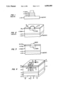
- FIG. 1 shows an InGaAs mesa photodiode representative of the prior art
- FIG. 2 shows an InGaAs planar photodiode representative of the prior art
- FIG. 3 shows a planar photodiode useful in describing the evolution of our invention.
- FIG. 4 shows a planar photodiode in accordance with an illustrative embodiment of our invention.
- the vertical interface between the p-electrical contact and the second silicon nitride layer, as well as the horizontal interface between the second silicon nitride layer and the semiconductor may not be perfect seals and therefore allow contaminants to migrate along the semiconductor surface to a crack in the first silicon nitride layer.
- This problem is exacerbated in the prior art photodiode of FIG. 2 where only a single silicon nitride layer is used, and an actual gap can exist between the contact and silicon nitride layer.
- Contaminants in the gap are not per se a problem because under reverse bias this undepleted region of semiconductor experiences essentially zero electric field.
- the contaminants on the surface would be essentially immobile and would not migrate to the p-n junction.
- a similar gap is created in the photodiode of FIG. 3 because it is extremely difficult to align the metal contact deposition mask to the opening in the second silicon nitride layer. Any lack of concentricity between the openings will result in an undesired gap around portions of the periphery.
- the vertical edge of the p-contact is very close (typically a few ⁇ m) to the edge of the p-n junction at the surface, and we have found that this configuration contributes to additional dark current.
- a photodiode with reduced dark current, low capacitance, high speed, and improved reliability comprises, as shown in FIG. 4, a Group III-V compound semiconductor body 10 having a major surface 12 on which are deposited a first silicon nitride layer 14, a second silicon nitride layer 16, and an electrical contact 18.
- body 10 includes a transparent substrate 11, a transparent epitaxial buffer layer 13, and a light-absorbing epitaxial layer 15.
- the first layer 14 has a first, typically circular, window W1 therein and serves both to partially passivate surface 12 and to mask the introduction (e.g., via diffusion) of dopants, thereby changing the conductivity type of zone 19 and defining the width W3 of p-n junction 20.
- Second layer 16 is deposited over first layer 14, and a second, typically circular, window W2 is opened therein so that windows W1 and W2 overlap one another but preferably so that window W2 is centered within window W1.
- Layer 16 serves to further passivate surface 12, as discussed above, and to mask the deposition (e.g., evaporation) of an ohmic electrical contact 18, thereby defining the width W2 of the bottom of the pedestal portion 18.1 of the contact.
- contact 18 is depicted as being symmetrical for purposes of illustration, it can also take on asymmetrical configurations.
- an annular contact 22 is formed on the bottom of body 10 (e.g., on substrate 11), and an anti-reflection (AR) coating 24 is formed in the annulus.
- Lightwaves 26 to be detected are directed through AR coating 24 and transparent layers 11 and 13 into light-absorbing layer 15. This absorption generates hole-electron pairs which are swept out of layer 15 by a reverse bias voltage applied between contacts 18 and 22 by a source illustratively depicted as a battery 28.
- the electron-hole pairs so collected produce a photocurrent which does useful work in a load R L .
- the advantages and features of the invention can be realized in a front illuminated embodiment using contact designs well-known in the art to permit light to enter light-absorbing layer 15 through the top surface of the photodiode.
- the p-i-n configuration is realized by making the light-absorbing layer 15 lightly doped n-type (e.g., ⁇ 5 ⁇ 10 15 cm 3 ) so that the p-type zone 19, n-type layer 15 and n-type layer 13 actually form a p-n - -n + junction.
- Maximum light-absorption efficiency is obtained by adjusting the doping and thickness of layer 15 such that this layer is fully depleted at normal diode operating voltages.
- the windows in the silicon nitride layers are mutually adapted so that the edges of the pedestal portion 18.1 of contact 18 are sufficiently remote from the edges of the junction 20 which intersect surface 12, thereby reducing strain and cracks in the high field region of the junction.
- the ratio of W1/W2 is preferably not less than about 3/1.
- the contact 18 has a cap portion 18.2 which overlaps the vertical interface 16.1 between silicon nitride layer 16 and pedestal portion 18.1, thereby sealing out potentially deleterious contaminants.
- the double dielectric layer provides better passivation than a single layer (even if the single layer is of the same thickness as the composite double layer); that is, the second silicon nitride layer 16 seals cracks in the first silicon nitride layer 14 which also prevents contaminants from shorting the p-n junction at the semiconductor surface.
- photodiode 10 comprised a (100)-oriented n-InP substrate 11 doped with sulphur to ⁇ 10 18 cm -3 and two layers 13 and 15 grown thereon by liquid phase epitaxy: an unintentionally doped n-InP buffer layer 13 and an unintentionally doped n-In 0 .53 Ga 0 .47 As layer 15. The latter had a carrier concentration of about 7-9 ⁇ 10 15 cm -3 . Diodes were also fabricated on tin-doped InP substrates.
- Zone 19 of p-In 0 .53 Ga 0 .47 As and p-n junction 20 were formed by diffusion of Zn through window W1 in a silicon nitride layer 14.
- the surface 12 of the wafer Prior to the deposition of the layer 14 the surface 12 of the wafer was etched in a dilute 1:1 aqueous HF solution for 4 minutes, then in a 0.5% solution of bromine in methanol for 10 seconds, followed by rinsing in methanol and deionized water.
- the silicon nitride layer 14 (about 1000 Angstroms thick) was deposited immediately following the surface preparation by reacting silane and ammonia in a commercial reactor. The substrate temperature during deposition was 350 degrees C.
- Zn was diffused at 550 degrees C.
- a second layer 16 of silicon nitride (about 1000 Angstroms thick) was plasma deposited on the first layer 14 using the same deposition parameters as for the first layer.
- a circular window of diameter W2, centered in the window W1 was photolithographically etched in the layer 16.
- the diameter of the cap portion not exceed W3, in order to avoid increasing device capacitance and leakage current.
- an AR coating 24 of silicon nitride was first plasma deposited by heating the wafer to 250 degrees C. and reacting silane and ammonia in a commercial reactor.
- the thickness of the AR coating was nominally 1800 Angstroms and its index of refraction 1.9.
- an infrared mask aligner ⁇ >1.7 ⁇ m
- an AR coated window 250 ⁇ m in diameter was defined on the n-side to be concentric with the contact 18.
- the silicon nitride on the substrate outside of the window was etched away, and a Au-Sn annular contact 22 was evaporated on the substrate to provide for the substrate contact.
- the contacts 18 and 22 were subsequently furnace alloyed by bringing the wafer to 420 degrees C. for 10 minutes in a forming gas atmosphere.
- the room-temperature, reverse current-voltage characteristic of a typical planar p-i-n photodiode as described above was measured.
- the value of the dark current at 10 V reverse bias was 5 nA, which is adequate for use with GaAs/FET receivers at, for example, 12 Mb/s data rates.
- Dark current histograms were plotted for three wafers, B1, B2, and B3 showing median dark current values of 7.9 nA, 4 nA and 8.4 nA, respectively. About 60% of all devices on each wafer had less than 10 nA dark currents.
- the lowest dark current value at -10 V on any of these wafers was 2.9 nA, corresponding to a current density of 5.8 ⁇ 10 -5 A/cm 2 .
- C-V capacitance-voltage
- the quantum efficiency was determined by comparing the photocurrent of a detector with that of a calibrated In 0 .53 Ga 0 .47 As photodiode.
- the source of radiation was a 1.28 ⁇ m LED coupled through a 50 ⁇ m core fiber butted up against the photosensitive region of the detector.
- Quantum efficiency measurements on devices from wafer B1 gave values of 87% ⁇ 2% corresponding to a typical responsivity of 0.90 A/W.
- the breakdown voltage defined as the voltage at which the dark current was 10 ⁇ A, was found to be about 50 V. Furthermore, the breakdown voltage values were found to be tightly distributed around their mean. For example, the devices of wafer B3 had breakdown voltage values of (50 ⁇ 3)V. Under a forward biasing current of 10 mA, the dynamic resistance of the restricted contact photodiodes was found to be (8 ⁇ 1) ⁇ . The response time of the p-i-n photodetectors was also measured by using as a source an InGaAsP laser emitting at 1.3 ⁇ m. The rise time of a typical device was found to be less than 0.23 nsec at a bias of -10 V.
- Photodiodes of this type are suitable for use in lightwave receivers with data rate capabilities of at least 1 Gb/sec. They may be used in lightwave receivers or as laser backface monitors in lightwave transmitters.
- the top surface of the semiconductor body need not be InGaAs and, in fact, in order to further reduce dark current may be a wider bandgap material such as InGaAsP or InP as described by O. K. Kim in copending application Ser. No. 609,317 filed on May 11, 1984 and assigned to the assignee hereof, now U.S. Pat. No. 4,608,586 issued on Aug. 26, 1986.
Abstract
Description
Claims (6)
Priority Applications (1)
| Application Number | Priority Date | Filing Date | Title |
|---|---|---|---|
| US07/464,505 US4990989A (en) | 1982-03-19 | 1990-01-12 | Restricted contact planar photodiode |
Applications Claiming Priority (2)
| Application Number | Priority Date | Filing Date | Title |
|---|---|---|---|
| US35998882A | 1982-03-19 | 1982-03-19 | |
| US07/464,505 US4990989A (en) | 1982-03-19 | 1990-01-12 | Restricted contact planar photodiode |
Related Parent Applications (1)
| Application Number | Title | Priority Date | Filing Date |
|---|---|---|---|
| US06/767,613 Continuation-In-Part US4894703A (en) | 1982-03-19 | 1985-08-20 | Restricted contact, planar photodiode |
Publications (1)
| Publication Number | Publication Date |
|---|---|
| US4990989A true US4990989A (en) | 1991-02-05 |
Family
ID=27000706
Family Applications (1)
| Application Number | Title | Priority Date | Filing Date |
|---|---|---|---|
| US07/464,505 Expired - Lifetime US4990989A (en) | 1982-03-19 | 1990-01-12 | Restricted contact planar photodiode |
Country Status (1)
| Country | Link |
|---|---|
| US (1) | US4990989A (en) |
Cited By (6)
| Publication number | Priority date | Publication date | Assignee | Title |
|---|---|---|---|---|
| US5731213A (en) * | 1992-07-28 | 1998-03-24 | Kabushiki Kaisha Toshiba | Semiconductor light receiving device and method of manufacturing the same |
| US20050004901A1 (en) * | 2003-07-04 | 2005-01-06 | Matsushita Electric Industrial Co., Ltd. | Data consistency detection device, data consistency detection method and data selection device |
| US20060001953A1 (en) * | 2004-06-30 | 2006-01-05 | Finisar Corporation | Linear optical amplifier using coupled waveguide induced feedback |
| US20060045157A1 (en) * | 2004-08-26 | 2006-03-02 | Finisar Corporation | Semiconductor laser with expanded mode |
| US20070263688A1 (en) * | 2004-06-30 | 2007-11-15 | Finisar Corporation | Semiconductor laser with side mode suppression |
| US20080308891A1 (en) * | 2007-06-13 | 2008-12-18 | Joseph Charles Boisvert | Ultra low dark current pin photodetector |
Citations (6)
| Publication number | Priority date | Publication date | Assignee | Title |
|---|---|---|---|---|
| US3287612A (en) * | 1963-12-17 | 1966-11-22 | Bell Telephone Labor Inc | Semiconductor contacts and protective coatings for planar devices |
| US3943621A (en) * | 1974-03-25 | 1976-03-16 | General Electric Company | Semiconductor device and method of manufacture therefor |
| US4019199A (en) * | 1975-12-22 | 1977-04-19 | International Business Machines Corporation | Highly sensitive charge-coupled photodetector including an electrically isolated reversed biased diffusion region for eliminating an inversion layer |
| US4062707A (en) * | 1975-02-15 | 1977-12-13 | Sony Corporation | Utilizing multiple polycrystalline silicon masks for diffusion and passivation |
| US4072541A (en) * | 1975-11-21 | 1978-02-07 | Communications Satellite Corporation | Radiation hardened P-I-N and N-I-P solar cells |
| US4110778A (en) * | 1977-06-21 | 1978-08-29 | The United States Of America As Represented By The Secretary Of The Air Force | Narrow-band inverted homo-heterojunction avalanche photodiode |
-
1990
- 1990-01-12 US US07/464,505 patent/US4990989A/en not_active Expired - Lifetime
Patent Citations (6)
| Publication number | Priority date | Publication date | Assignee | Title |
|---|---|---|---|---|
| US3287612A (en) * | 1963-12-17 | 1966-11-22 | Bell Telephone Labor Inc | Semiconductor contacts and protective coatings for planar devices |
| US3943621A (en) * | 1974-03-25 | 1976-03-16 | General Electric Company | Semiconductor device and method of manufacture therefor |
| US4062707A (en) * | 1975-02-15 | 1977-12-13 | Sony Corporation | Utilizing multiple polycrystalline silicon masks for diffusion and passivation |
| US4072541A (en) * | 1975-11-21 | 1978-02-07 | Communications Satellite Corporation | Radiation hardened P-I-N and N-I-P solar cells |
| US4019199A (en) * | 1975-12-22 | 1977-04-19 | International Business Machines Corporation | Highly sensitive charge-coupled photodetector including an electrically isolated reversed biased diffusion region for eliminating an inversion layer |
| US4110778A (en) * | 1977-06-21 | 1978-08-29 | The United States Of America As Represented By The Secretary Of The Air Force | Narrow-band inverted homo-heterojunction avalanche photodiode |
Non-Patent Citations (23)
| Title |
|---|
| "Ga0.47 In0.53 As: A Ternary Semiconductor for Photodetector Applications"; IEEE Journal of Quantum Electronics, vol. QE-16, (1980), pp. 709-720, T. P. Pearsall. |
| "In0.53 Ga0.47 As p-i-n Photodiodes For Long-Wavelength Fiber-Optic Systems", Electronics Letters, vol. 15, No. 22, (1979); pp. 713-715, R. F. Leheny et al. |
| "InGaAs Avalanche Photodiode With InP p-n Junction", Electronics Letters, vol. 16, No. 5, pp. 163-165, Feb. 1980, H. Kanbe et al. |
| "InP/InGaAs Heterojunction Phototransistors", IEEE Journal of Quantum Electronics, vol. QE-17, No. 2 (Feb. 1981); pp. 264-269, J. C. Campbell et al. |
| "Low Dark-Current, High-Efficincy Planar In0.53 Ga0.47 As/InP Pin Photodiodes", Electron Device Letters, vol. EDL-2, No. 11, Nov. 1981, pp. 283-285, S. R. Forrest et al. |
| "Planar Photodiodes Made From Vapour-Phase Epitaxial Inx Ga1-x As", Electronics Letters, vol. 15, No. 8, pp. 238-240, (Apr. 1979), N. Susa et al. |
| "Planar Type Vapor-Phase Epitaxial In0.53 Ga0.47 As Photodiode", IEEE Electron Device Letters, EDL-1, No. 4 (Apr. 1980), pp. 55-57, N. Susa et al. |
| "Small Area InGaAs/InP p-i-n Photodiodes: Fabrication, Characteristics and Performance of Devices in 274 Mb/s and 45 Mb/s, Lightwave Receivers at 1:31 μm Wavelength", Electronics Letters, vol. 16, No. 4, pp. 155-156 (Feb. 14, 1980), T. P. Lee et al. |
| "Zn-diffused In0.53 Ga0.47 As/InP avalanche photodetector", Applied Physics Letters, vol. 35, No. 6, (Sep. 15, 1979), pp. 466-468, Y. Matsushima et al. |
| Electronics , p. 77, Sep. 4, 69. * |
| Electronics publication, Aug. 4, 1969, vol. 42, No. 6. * |
| Electronics, p. 77, Sep. 4, 69. |
| Forrest, S. R., "Low Dark Current High Efficiency Planar InGaAs/InP P-rN Photodiodes", IEEE Elec. Dev. Letrs., vol. EDL-2 #11, pp. 283-285, Nov. 81. |
| Forrest, S. R., Low Dark Current High Efficiency Planar InGaAs/InP P rN Photodiodes , IEEE Elec. Dev. Letrs., vol. EDL 2 11, pp. 283 285, Nov. 81. * |
| Ga 0.47 In 0.53 As: A Ternary Semiconductor for Photodetector Applications ; IEEE Journal of Quantum Electronics , vol. QE 16, (1980), pp. 709 720, T. P. Pearsall. * |
| In 0.53 Ga 0.47 As p i n Photodiodes For Long Wavelength Fiber Optic Systems , Electronics Letters , vol. 15, No. 22, (1979); pp. 713 715, R. F. Leheny et al. * |
| InGaAs Avalanche Photodiode With InP p n Junction , Electronics Letters , vol. 16, No. 5, pp. 163 165, Feb. 1980, H. Kanbe et al. * |
| InP/InGaAs Heterojunction Phototransistors , IEEE Journal of Quantum Electronics , vol. QE 17, No. 2 (Feb. 1981); pp. 264 269, J. C. Campbell et al. * |
| Low Dark Current, High Efficincy Planar In 0.53 Ga 0.47 As/InP Pin Photodiodes , Electron Device Letters, vol. EDL 2, No. 11, Nov. 1981, pp. 283 285, S. R. Forrest et al. * |
| Planar Photodiodes Made From Vapour Phase Epitaxial In x Ga 1 x As , Electronics Letters , vol. 15, No. 8, pp. 238 240, (Apr. 1979), N. Susa et al. * |
| Planar Type Vapor Phase Epitaxial In 0.53 Ga 0.47 As Photodiode , IEEE Electron Device Letters, EDL 1, No. 4 (Apr. 1980), pp. 55 57, N. Susa et al. * |
| Small Area InGaAs/InP p i n Photodiodes: Fabrication, Characteristics and Performance of Devices in 274 Mb/s and 45 Mb/s, Lightwave Receivers at 1:31 m Wavelength , Electronics Letters , vol. 16, No. 4, pp. 155 156 (Feb. 14, 1980), T. P. Lee et al. * |
| Zn diffused In 0.53 Ga 0.47 As/InP avalanche photodetector , Applied Physics Letters , vol. 35, No. 6, (Sep. 15, 1979), pp. 466 468, Y. Matsushima et al. * |
Cited By (9)
| Publication number | Priority date | Publication date | Assignee | Title |
|---|---|---|---|---|
| US5731213A (en) * | 1992-07-28 | 1998-03-24 | Kabushiki Kaisha Toshiba | Semiconductor light receiving device and method of manufacturing the same |
| US20050004901A1 (en) * | 2003-07-04 | 2005-01-06 | Matsushita Electric Industrial Co., Ltd. | Data consistency detection device, data consistency detection method and data selection device |
| US20060001953A1 (en) * | 2004-06-30 | 2006-01-05 | Finisar Corporation | Linear optical amplifier using coupled waveguide induced feedback |
| US7057803B2 (en) | 2004-06-30 | 2006-06-06 | Finisar Corporation | Linear optical amplifier using coupled waveguide induced feedback |
| US20070263688A1 (en) * | 2004-06-30 | 2007-11-15 | Finisar Corporation | Semiconductor laser with side mode suppression |
| US7711016B2 (en) | 2004-06-30 | 2010-05-04 | Finisar Corporation | Semiconductor laser with side mode suppression |
| US20060045157A1 (en) * | 2004-08-26 | 2006-03-02 | Finisar Corporation | Semiconductor laser with expanded mode |
| US20080308891A1 (en) * | 2007-06-13 | 2008-12-18 | Joseph Charles Boisvert | Ultra low dark current pin photodetector |
| US7598582B2 (en) * | 2007-06-13 | 2009-10-06 | The Boeing Company | Ultra low dark current pin photodetector |
Similar Documents
| Publication | Publication Date | Title |
|---|---|---|
| US6794631B2 (en) | Three-terminal avalanche photodiode | |
| JP3141847B2 (en) | Avalanche photodiode | |
| Stillman et al. | III-V compound semiconductor devices: Optical detectors | |
| Lee et al. | InGaAs/InP pin photodiodes for lightwave communications at the 0.95-1.65 µm wavelength | |
| CA1256549A (en) | Avalanche photodiode made by mesa etch process | |
| Susa et al. | Characteristics in InGaAs/InP avalanche photodiodes with separated absorption and multiplication regions | |
| EP0181391B1 (en) | Back-illuminated photodiode with wide bandgap cap layer | |
| EP1063709B1 (en) | Method of fabricating a surface coupled InGaAs photodetector | |
| US4894703A (en) | Restricted contact, planar photodiode | |
| US4700209A (en) | Avalanche photodiode and a method of making same | |
| US5315148A (en) | Photo-sensing device | |
| Kaneda | Silicon and germanium avalanche photodiodes | |
| US6262465B1 (en) | Highly-doped P-type contact for high-speed, front-side illuminated photodiode | |
| US4587544A (en) | Avalanche photodetector | |
| US4990989A (en) | Restricted contact planar photodiode | |
| US4586067A (en) | Photodetector with isolated avalanche region | |
| US4586066A (en) | Avalanche photodetector | |
| US4396443A (en) | Reduction of leakage current in InGaAs diodes | |
| JPH07118548B2 (en) | III-V group compound semiconductor PIN photo diode | |
| JPH08274366A (en) | Semiconductor light receiving device | |
| Sloan | Photodetectors | |
| Yeats et al. | Detailed performance characteristics of hybrid InP-InGaAsP APD's | |
| CN112382687A (en) | Planar photoelectric detector and preparation method thereof | |
| JPS6259905B2 (en) | ||
| JPH0722641A (en) | Photodetector |
Legal Events
| Date | Code | Title | Description |
|---|---|---|---|
| AS | Assignment |
Owner name: BELL TELEPHONE LABORATORIES, INCORPORATED, A CORP. Free format text: ASSIGNMENT OF ASSIGNORS INTEREST.;ASSIGNORS:ELHAMAMSY, MAHMOUD A.;FORREST, STEPHEN R.;ZUBER, JOHN R.;REEL/FRAME:005222/0606;SIGNING DATES FROM 19900102 TO 19900109 Owner name: AMERICAN TELEPHONE AND TELEGRAPH COMPANY, A CORP. Free format text: ASSIGNMENT OF ASSIGNORS INTEREST.;ASSIGNORS:ELHAMAMSY, MAHMOUD A.;FORREST, STEPHEN R.;ZUBER, JOHN R.;REEL/FRAME:005222/0606;SIGNING DATES FROM 19900102 TO 19900109 |
|
| STCF | Information on status: patent grant |
Free format text: PATENTED CASE |
|
| FEPP | Fee payment procedure |
Free format text: PAYOR NUMBER ASSIGNED (ORIGINAL EVENT CODE: ASPN); ENTITY STATUS OF PATENT OWNER: LARGE ENTITY |
|
| FPAY | Fee payment |
Year of fee payment: 4 |
|
| FEPP | Fee payment procedure |
Free format text: PAYOR NUMBER ASSIGNED (ORIGINAL EVENT CODE: ASPN); ENTITY STATUS OF PATENT OWNER: LARGE ENTITY Free format text: PAYER NUMBER DE-ASSIGNED (ORIGINAL EVENT CODE: RMPN); ENTITY STATUS OF PATENT OWNER: LARGE ENTITY |
|
| FEPP | Fee payment procedure |
Free format text: PAYER NUMBER DE-ASSIGNED (ORIGINAL EVENT CODE: RMPN); ENTITY STATUS OF PATENT OWNER: LARGE ENTITY Free format text: PAYOR NUMBER ASSIGNED (ORIGINAL EVENT CODE: ASPN); ENTITY STATUS OF PATENT OWNER: LARGE ENTITY |
|
| FPAY | Fee payment |
Year of fee payment: 8 |
|
| FEPP | Fee payment procedure |
Free format text: PAYER NUMBER DE-ASSIGNED (ORIGINAL EVENT CODE: RMPN); ENTITY STATUS OF PATENT OWNER: LARGE ENTITY Free format text: PAYOR NUMBER ASSIGNED (ORIGINAL EVENT CODE: ASPN); ENTITY STATUS OF PATENT OWNER: LARGE ENTITY |
|
| FPAY | Fee payment |
Year of fee payment: 12 |