US4983834A - Large area particle detector system - Google Patents
Large area particle detector system Download PDFInfo
- Publication number
- US4983834A US4983834A US07/203,324 US20332488A US4983834A US 4983834 A US4983834 A US 4983834A US 20332488 A US20332488 A US 20332488A US 4983834 A US4983834 A US 4983834A
- Authority
- US
- United States
- Prior art keywords
- electron trapping
- dopant
- trapping material
- pattern
- radiation
- Prior art date
- Legal status (The legal status is an assumption and is not a legal conclusion. Google has not performed a legal analysis and makes no representation as to the accuracy of the status listed.)
- Expired - Lifetime
Links
Images


Classifications
-
- C—CHEMISTRY; METALLURGY
- C09—DYES; PAINTS; POLISHES; NATURAL RESINS; ADHESIVES; COMPOSITIONS NOT OTHERWISE PROVIDED FOR; APPLICATIONS OF MATERIALS NOT OTHERWISE PROVIDED FOR
- C09K—MATERIALS FOR MISCELLANEOUS APPLICATIONS, NOT PROVIDED FOR ELSEWHERE
- C09K11/00—Luminescent, e.g. electroluminescent, chemiluminescent materials
- C09K11/08—Luminescent, e.g. electroluminescent, chemiluminescent materials containing inorganic luminescent materials
- C09K11/77—Luminescent, e.g. electroluminescent, chemiluminescent materials containing inorganic luminescent materials containing rare earth metals
- C09K11/7783—Luminescent, e.g. electroluminescent, chemiluminescent materials containing inorganic luminescent materials containing rare earth metals containing two or more rare earth metals one of which being europium
- C09K11/7784—Chalcogenides
- C09K11/7786—Chalcogenides with alkaline earth metals
-
- G—PHYSICS
- G01—MEASURING; TESTING
- G01T—MEASUREMENT OF NUCLEAR OR X-RADIATION
- G01T1/00—Measuring X-radiation, gamma radiation, corpuscular radiation, or cosmic radiation
- G01T1/02—Dosimeters
- G01T1/10—Luminescent dosimeters
- G01T1/11—Thermo-luminescent dosimeters
-
- G—PHYSICS
- G01—MEASURING; TESTING
- G01T—MEASUREMENT OF NUCLEAR OR X-RADIATION
- G01T1/00—Measuring X-radiation, gamma radiation, corpuscular radiation, or cosmic radiation
- G01T1/16—Measuring radiation intensity
- G01T1/20—Measuring radiation intensity with scintillation detectors
- G01T1/2012—Measuring radiation intensity with scintillation detectors using stimulable phosphors, e.g. stimulable phosphor sheets
- G01T1/2014—Reading out of stimulable sheets, e.g. latent image
-
- G—PHYSICS
- G11—INFORMATION STORAGE
- G11C—STATIC STORES
- G11C13/00—Digital stores characterised by the use of storage elements not covered by groups G11C11/00, G11C23/00, or G11C25/00
- G11C13/04—Digital stores characterised by the use of storage elements not covered by groups G11C11/00, G11C23/00, or G11C25/00 using optical elements ; using other beam accessed elements, e.g. electron or ion beam
Definitions
- the present invention relates generally to the detection and recording of nuclear particles. More particularly, the present invention relates to a system for detecting and recording the impingement of a nuclear particle on a two-dimensional position-sensitive solid-state detector.
- detectors are generally semiconductor devices in which the radiation absorption and detection occur in the same material, for example, silicon or germanium diodes, or scintillator media mated with photo-multiplier tubes in which the configuration of light produced in the scintillator is detected by the photo-multiplier tube.
- Radiographic films have the additional drawback that they do not allow for easy retrieval of the stored information relating to the detected impingement of the radiation particles.
- semiconductor detectors have generally been the most useful for particulate radiation, because the range of the particles is usually less than the depletion region depth of the detectors. Such semiconductor detectors have good energy resolution, excellent timing characteristics, good stability and simplicity of operation. However, the area of such detectors has been limited to approximately 20 cm 2 or less. Thus, the necessity for arraying individual detectors.
- thermoluminescent phosphor layer provided on a support base for recording the impingement of radiation thereon.
- the radiation energy corresponding to the radiation impingement is released as a light signal which can then be detected.
- a major drawback of that type of detector is that the use of a heat-stimulable phosphor requires that the panel or support base upon which the thermoluminescent phosphor is placed be extremely heat resistant.
- the response time of such a detector is very slow due to the thermal time constants involved.
- the use of a CO 2 laser limits the position resolution achievable to 10 microns or greater.
- U.S. Pat. No. 3,859,527 discloses an apparatus which does not utilize the input of heat energy in order to release the stored radiation pattern.
- the stimulable phosphor utilized in that patent is a visible ray or infrared ray stimulable phosphor and visible rays or infrared rays are utilized as the stimulation energy. Visible rays or infrared rays are used in order to convert the radiation energy stored in the apparatus to a light signal.
- phosphors such as cerium and samarium activated strontium sulfide, a europium and samarium activated strontium sulfide, a europium and samarium activated lanthanum oxysulfide phosphor and a manganese and halogen activated zinc cadmium sulfide phosphor which can be used.
- the sensitivity of the method disclosed in the '527 patent and the phosphors employed therein is very low because the stimulability of such phosphors is very low.
- the method and apparatus disclosed in the '527 patent is of little practical use. Contrary to the statement at column 4, lines 11-12 of that patent, applicants have found that the cerium and samarium activated strontium sulfide composition is sensitive to tungsten light.
- U.S. Pat. No. 4,239,968 discloses yet another method and apparatus for recording and reproducing a radiation image in which the radiation image is recorded on a stimulable phosphor and the recorded image is reproduced by utilizing the stimulability of the phosphor.
- the phosphor disclosed for use in that patent is an alkaline earth metal fluorohalide phosphor which is claimed to have high stimulability.
- the phosphor disclosed in that patent is represented by the formula (Ba l-x M x II ) FX:yA, in which M II is at least one divalent metal selected from the group consisting of Mg, Ca, Sr, Zn and Cd, X is at least one halogen selected from the group consisting of Cl, Br and I, A is at least one element selected from the group consisting of Eu, Tb, Ce, Tm, Dy, Pr, Ho, Nd, Yb and Er, preferably selected from the group consisting of Eu, Tb, Ce and Tm and x and y are numbers satisfying the conditions of 0 is less than or equal to x is less than or equal to 0.6 and 0 is less than or equal to y which is less than or equal to 0.2.
- the method described in the '968 patent comprises the steps of causing a visible ray or infrared ray-stimulable phosphor to absorb radiation passing through an object, stimulating the phosphor by stimulation rays selected from visible rays and infrared rays in order to release the energy of the radiation stored therein as luminescence and detecting the luminescence.
- the stimulation rays are described as having a wavelength of not less than 500 nm.
- the apparatus utilized for such recording and reproducing of a radiation image is comprised of a radiation image storage panel using a stimulable phosphor which absorbs radiation passing through an object, a light source emitting stimulation rays of not less than 500 nm in order to release the energy of the radiation stored in the phosphor as luminescence and a detector for detecting that luminescence.
- the stimulable phosphor is at least one phosphor selected from the group of the above-mentioned alkaline earth metal fluorohalide phosphors.
- the method and apparatus set forth in the '968 patent has many drawbacks.
- the intensity of the stimulating radiation is very high.
- the efficiency of the phosphor disclosed therein is not efficient enough to be utilized as a relatively large area particle detector because of the sensitivity of the phosphors disclosed therein with regard to the area to be covered.
- a further drawback of the method and apparatus disclosed in the '968 patent is that it cannot be utilized with readily available low cost infrared sources, for example, laser diodes, since utilization of halide/phosphors require helium-neon ruby lasers.
- Another drawback to the method and apparatus disclosed in the '968 patent is that it has been found in use that the depth of the traps of the materials disclosed therein is insufficient for the storage of energy over a long period of time. Still another drawback to the '968 device is that it cannot readily utilize infrared wavelengths for both stimulation and emission since good separation between the stimulating and emitted wavelengths is required.
- the present invention is directed to detecting impingement of nuclear particles with position sensing over large areas in which the detector provides instantaneous local scintillation at visible wavelengths upon nuclear particle impingement.
- storage of a trap charge at such locations is also provided which can later be interrogated and read by the application of near-infrared illumination.
- illumination may be readily provided by solid state sources such as infrared-emitting diodes or laser diodes.
- the solid-state materials utilized by the present invention are a family of materials known as alkaline earth sulfides and selenides that have highly unusual properties. These particular materials display efficient electron trapping and are called electron trapping materials. These materials can be "charged" by light.
- thermoluminescence was observed in ordinary limestones and granites. While that effect could only be observed once, the emission properties of the limestones and granites could be restored by irradiation by x-rays or gamma rays.
- the effect was studied in detail and reported by F. Daniels, et al, "The Thermoluminescence of Crystals", Report On Contract AT(11-1) -27, University of Wisconsin, Madison, Wis. A general model involving trapped electrons was later accepted. See, "Electronic Processes in Ionic Crystals", N. F. Mott and R. W. Gurney, Oxford University Press, New York, 1940.
- the method and apparatus of the present invention releases the trapped electrons by use of infrared or near-infrared radiation.
- the dose can be "read" by, for example, infrared pulses. Such pulses will release the trapped electrons and supply an analog of the integrated dose for the previous time interval in the form of the integral released intensity of orange or blue light.
- the device described herein can be termed a photonic detector.
- the present application is directed to the use of such material to large areas which can be used in many different environments as a nuclear particle detector and event locator with memory.
- luminescence which is understood to be the ability of certain solids to emit light under different conditions.
- luminescence refers to the ability of certain solids and liquids to emit light when driven by an external energy source
- the proper term for that phenomenon is photoluminescence.
- certain photoluminescent materials will emit light when driven by radiation of short wavelengths, such as ultraviolet
- the present invention relates to that class of materials with the unique properties of electron traps.
- optical communications can be accomplished, as well as making infrared radiation patterns visible.
- in a light-to-light photonics mode such materials will be used in digital processing or so-called "light" computers.
- Another object of the present invention is to provide a reliable and relatively inexpensive method of and apparatus for detecting, storing and analyzing the existence of certain nuclear particles within a specified environment.
- a further object of the present invention is to provide a method of and apparatus for reading the stored particle or pattern information from the large area particle detector electron trapping material utilizing infrared or near-infrared energy which, upon impinging upon the large area particle detector electron trapping composition, releases light of a predetermined range of wavelengths.
- Still another object of the present invention is to provide a method of and apparatus for erasing the stored nuclear particle information embodied by the electron trapping material of the large area particle detector so that such particle detector can be reused.
- a nuclear particle detector system having a large area particle detector with a surface area of at least 100 cm 2 which contains either a thick or thin film electron trapping material.
- a nuclear particle detector system having a large area particle detector with a surface area of at least 100 cm 2 which contains either a thick or thin film electron trapping material.
- the detector system can utilize the packet of visible light given off during impingement or, in a preferred embodiment, a solid-state light source placed facing either the front or back of the large area particle detector is utilized to release the stored electrons to allow them to move to a lower energy level, which results in the giving off of light at a certain predetermined range of wavelengths having a peak about a predetermined wavelength, depending upon the composition of the electron trapping material.
- This "reading" of the stored nuclear particle information can take place up to years after the original impingement of the nuclear particles.
- the release of the stored nuclear particle information in the form of light of a predetermined wavelength corresponds to the x-y position of impingement of the detected nuclear particles and is linearly related to the flux or rate of change and/or number or pattern of detected particles.
- the released stored energy does not need to be filtered and is thus sensed in order to provide an electrical signal corresponding to the particle events recorded on the large area particle detector.
- Both the filter if any, recording medium and sensor and other associated optics which may be utilized are contained within a light-tight enclosure.
- the electrical signal is then analyzed by a conventional microcomputer. In order to erase the information stored on the large area particle detector, a near-infrared or infrared source of radiation can be utilized.
- the large area particle detector of the present invention can be read many times by use of a pulsed infrared or near-infrared solid-state source, without significantly depleting the stored information on the particle detector.
- a much higher intensity or different wavelength infrared or near-infrared radiation source may be utilized which is preferably used in a continuous transmission mode instead of the pulsed mode of the "reading" source. If it is desired to obtain the integral of the stored photon energy, then a high intensity radiation source is utilized, which also functions to "erase” the stored energy from the detector. If operating in a scanning mode, it is also possible to operate the reading source in a continuous wave mode.
- the apparatus aspects of the invention may be accomplished utilizing an x-y stepping stage containing a near-infrared semiconductor diode laser which "reads" the stored nuclear particle information pattern from the large area particle detector.
- a photo-multiplier tube may function as a sensor for reading the released light energy and converting that light energy to electrical signals.
- the method of the present invention may be carried out by a large area particle detector which includes a thick or thin film of electron trapping material which provides the means for detecting and storing the existence of the previous impingement of nuclear particles and the position and intensity thereof within its environment.
- the impingement of nuclear particles may be read instantaneously by means of a sensor for sensing the visible light energy which is given off by the large area particle detector electron trapping material upon impingement of the nuclear particles.
- the method of the present invention may also be effectuated by means of later readout by an infrared or near-infrared radiation source. In either event, the light energy released is converted to an electrical signal by an appropriate sensor and then analyzed by, for example, a conventional microcomputer.
- FIG. 1 is a schematic block diagram of a system for detecting nuclear particles utilizing a large area particle detector
- FIG. 2 is a schematic block diagram of another embodiment of a system for detecting nuclear particles utilizing a large area particle detector
- FIG. 3 is a diagram illustrating a top view of a thick film embodiment of a large area particle detector for use with the system shown in FIGS. 1 and 2;
- FIG. 4 is a diagram of a side view of one of the plurality of blocks which make up the large area particle detector shown in FIG. 3;
- FIG. 4a is a diagram of a side view of an alternative embodiment of one of the plurality of blocks which make up the large area particle detector shown in FIG. 3;
- FIG. 5 is a diagram of a side view of a two layer embodiment of a thin film embodiment of a large area particle detector for use with the systems of FIGS. 1 and 2;
- FIG. 6 is a diagram of a side view of a three layer thin film embodiment of a large area particle detector for use with the systems of FIGS. 1 and 2;
- FIG. 7 is a diagram of a side view of a four layer thin film embodiment of a large area particle detector for use with the systems of FIGS. 1 and 2;
- FIG. 8 is a diagram of yet another embodiment of the large area nuclear particle detector system of the present invention showing that portion of FIG. 1 suitably configured for detection of alpha particles;
- FIG. 9 is a pictorial diagram of a hard-surface alpha probe using the thin film large area particle detector shown in FIG. 7;
- FIG. 10 is a graph showing the relationship between the dose of radiation impinging on the large area particle detector of the present invention and the released energy per area of the detector emitted as a result of reading the stored previously impinged radiation.
- FIG. 1 a particle detection system 10 for use with a large area particle detector 12, fabricated as will be described later herein.
- Incoming particles 14 impinge upon the large area particle detector 12, causing electrons therein to be raised up in energy level to a trapped state as has been briefly described herein. Due to the use of the electron trapping materials in constructing the particle detector, visible scintillation occurs as nuclear particles 14 impinge on the detector 12.
- means are provided for subsequently detecting the nuclear particle impingement information pattern stored in the electron trapping material of the detector 12, by means of the visible-wavelength luminescence produced by near-infrared interrogation using an infrared emitting diode 16.
- the diode 16 may preferably have a wavelength centered about 960 nm.
- a laser having a similar wavelength or other solid state device could also be utilized.
- the diode 16 is powered by an appropriate constant current supply 18.
- a second infrared or near infrared light source 20 which may be operated at a higher power level or at a different wavelength, can be utilized to "erase" the impingement pattern, when desired.
- the output of both diodes is controlled by setting its input current utilizing the regulated constant current power supply 18.
- the pulsing of the diode 16 serves to provide the stimulation for releasing the trapped electrons in the electron trapping (ET) material contained in the large area particle detector 12 to produce visible luminescence.
- the luminescence exiting from the rear (as shown in FIG. 1) of the large area particle detector 12, is reflected by a mirror 15 and passes first through a short-pass filter 22 in order to block near-infrared wavelength signals, and then through the image intensifier and zoom optics 24 until the luminescence impinges upon a luminescence sensor 26.
- the shortpass filter may preferably be a 650 nm wavelength filter.
- the entire detector system 10 is contained within a light-tight housing 28 having a window 13 which is transparent to alpha, beta, gamma and x-rays, but not to ambient or lower energy light.
- the sensor 26 may be either a photo-multiplier tube, such as a Hamamatsu Model R268 photo-multiplier tube, or can be configured as a parallel opto-electronic image capture array, such as the EG & G Reticon 256 ⁇ 256 device.
- the sensor 26 may be a Fairchild CCD 222 camera chip with a micro-channel plate intensifier and zoom optics 24. In the event that the EG & G Reticon diode array is utilized, it may not be necessary to use the image intensifier and zoom optics 24.
- the infrared source 20 when it is desired to erase the stored light images, the infrared source 20 is turned on continuously for a brief period of time. It should also be understood that the readout of the stored electrons can be accomplished from either side of the large area particle detector 12, assuming there is no reflective coating applied to that side. Thus, with the large area particle detector 12 as shown in FIG. 1, either infrared source 16 or 20 could be configured on either side of the detector 12 to either read out or erase the stored light images on the large area particle detector 12, depending upon its operating conditions and provided that light-tight conditions are still maintained.
- the output from the sensor 26 can readily be analyzed by a computer 30, such as a commercially available microcomputer.
- a computer 30 such as a commercially available microcomputer.
- the system is capable of a resolution of a "pixel" size of approximately 400 micrometers.
- the system is capable of examining storage pixels of about 10 microns in size over smaller areas of interest, for example, 25 mm ⁇ 25 mm.
- FIG. 2 A second embodiment of the large area particle detection system 10 is shown in FIG. 2.
- the infrared source 16a is secured to an x-y stepping stage 32, such as that available from Aerotech for serial scan-readout.
- the x-y stepping stage 32 serves to scan the stored electron population in a pixel-by-pixel manner, using a focused semiconductor diode laser 16a.
- the output from the sensor 26 is analyzed by the microcomputer 30.
- the illumination sources 16 and 16a may also be by near-infrared devices having wavelengths in the range 0.8 to 1.4 microns or 800 to approximately 1400 nm.
- Such a system provides built-in storage of particle impingement as well as rapid readout upon command.
- Such a system may be utilized, for example, in industrial or medical radiography with laser-diode readout of the stored images. It may also be utilized in biomedical radio tracer mapping in electrophoresis separation.
- FIGS. 3-7 there is shown therein various constructions for the large area particle detector 12.
- detectors can be broken down into two general categories in which the electron trapping materials utilized with the large area particle detector 12 are useful. They are detectors in which the particulate radiation gives up its energy in the material that stores the information and detectors in which light is produced in one material and the event information provided by that light is detected and stored in another material.
- Detectors of the first type are suitable for the detection of non-relativistic particles and are similar to commonly available detectors that use scintillators.
- Detectors of the second type are useful for the detection of Cerenkov radiation from the passage of relativistic particles.
- light produced in either quartz or sapphire will generate trapped electrons in the electron trapping material, thereby storing event information for subsequent retrieval.
- the formulation of electron trapping material required for Cerenkov radiation detection may be different from that required for non-relativistic particle detection because the process leading to the generation of trapped electrons is different.
- the material for Cerenkov detection and storage need only be sensitive to light wavelengths between 300 and 600 nm and need have little sensitivity to higher energy processes.
- a sensitivity for higher energy processes is required.
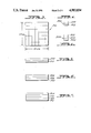
- the thick film material composition disclosed in such co-pending applications may be compressed into rods or other shapes and fired until it is a high density solid. Wafers are then sliced from the rods and polished. Wafer thicknesses are preferably in excess of 0.025 cm. Each of those wafers, which may preferably be of a circular or rectangular shape, are sized such that they may be mosaicked to fill the desired detection area.
- FIG. 3 illustrates a mosaicking of a plurality of those wafers, having a rectangular shape, on a substrate.
- FIG. 4 is a side view of one of the wafers 300 showing the substrate 302 to which the wafers 300 are attached and the thick film phosphor material 304.
- the various substrate materials and phosphor compositions are as disclosed in the aforementioned co-pending patent applications.
- an aluminum reflecting film 306 may be deposited on one surface of the polished wafers 300 so as to enhance the output luminescence produced by the infrared light exposure. Such a structure is shown in FIG. 4a.
- the infrared or near-infrared source used to read the stored electrons may be configured to impinge on either the front or back of the large area particle detector 12.
- the illuminating and erasing infrared sources 16 and 20, respectively would be arranged to impinge upon the opposite surface of the particle detector 12.
- FIGS. 5-7 A second embodiment of the large area particle detector 12 is shown in FIGS. 5-7.
- a thin film 308 is deposited on an appropriate substrate 310.
- the thin film 308 may preferably be in excess of 10 microns in thickness.
- the thin film layer 308 may be deposited onto a sapphire substrate 310.
- alternative substrates such as quartz, glass or plastic may also be used. It is important to note that all of the components in the source material used to create the thin film layer 308 be transferred to the substrate 310 so that the resultant film 308 is uniform in composition and closely approximates the desired material composition a set forth in the co-pending applications.
- Such a structure can be accomplished by utilizing a very rapid electron beam evaporation, preferably at a rate of between 10-20 nm per second, of a small slug of an appropriate phosphor composition.
- appropriate phosphors are disclosed, for example, in the assignee's U.S. Pat. No. 4,812,660 entitled Photoluminescent Materials for Outputting Yellow-Green Light; and U.S. Pat. No. 4,855,603 entitled Photoluminescent Materials for Radiography. The disclosure of both of those patents is incorporated by reference herein.
- Films prepared as described above could readily also be used as Cerenkov radiation detectors and storage media. Those thin films can also serve as detectors of low energy particulate radiation with the range of the various particles approximately corresponding to the film thickness for best detection capability. Utilizing either thick films or thin films, it is possible to detect both alpha particles, beta particles, and gamma particles, as well as x-rays or other particles.
- FIG. 6 is a side view of an alternative embodiment to FIG. 5 of the large area particle detector 12.
- Three layers are utilized in the embodiment of FIG. 6, namely a substrate layer 310, a thin film layer 308 and a reflecting layer 306, as previously described.
- FIG. 7 shows a side view of a third alternative embodiment for the large area particle detector 12 which utilizes a substrate 310 which may preferably be of 1 mm in thickness, a thin film scintillator layer 308 (alternatively referred to hereafter as “thin film 308" or “scintillator screen 308”); which is of thickness matched to the alpha particle range of an inorganic thin film scintillator material, which is disclosed in U.S. Pat. Nos. 4,855,603 and 4,812,659.
- These particular thin films are very resistant to permanent radiation damage and offer built-in selective radiation sensitivity because gamma and beta particles will generally be more readily transmitted by the film 308, but alpha particles will be nearly fully absorbed.
- the thin thin film scintillator layer 308 may be preferably coated with a 500 Angstroms thickness layer of aluminum 306 in order to enhance photon reflectance towards the detector.
- a corrosion-protection coating 314, as will be described later herein, may preferably be deposited directly on top of the aluminum layer 306 and may preferably be a layer of approximately 1 micrometer in thickness.
- Materials which may be used for the alpha window layer include nickel, chrome, nickel-chrome alloy, titanium, and vanadium. Such a layer of, for example, chromium, would provide many orders of magnitude greater abrasion resistance than the commonly used 0.25 mil (6 microns) aluminized free standing mylar membrane which scratches and tears, and could readily be formed onto 100 cm 2 surfaces by either chemical plating or evaporation methods, both of which can yield pinhole free coatings down to a micron in thickness.
- the structure of FIG. 7 may form a multilayer scintillator structure in which the alpha window 314 and scintillator screen 308 can be formed as a single plate.
- FIG. 8 there is shown therein a pictorial diagram of yet another embodiment of a large area particle detector system 10.
- This particular detector system 10 is designed for the detection and storage of information relating to alpha particles 82.
- a scintillator or large area particle detector 84 is used as a detector upon which the alpha particles 82 impinge.
- the large area alpha particle detector 84 may preferably be of a rectangular shape and measure at least 1 cm on a side, however it could also be constructed of a much larger size, for example a square meter.
- the scintillator 84 is placed at one end of a light-proof enclosure 28 having an opening 86 which is somewhat smaller than the width and the height of the scintillator 84.
- the scintillator 84 may be constructed from materials as described in connection with and shown in FIG. 7.
- a funnel-shaped light guide 88 which is of a hollow cone shape sized to an appropriate size for the detector or scintillator 84, may be used to "capture” and guide the light produced upon impingement of an alpha particle 82 on the scintillator 84.
- the hollow cone light guide 88 may be coated with a highly reflecting material on the inside and acts essentially as an integrating sphere.
- the luminescence produced upon impingement of an alpha particle may be coupled directly into a quartz-like guide which would be tapered in a similar manner to contain the scintillator or detector 84 at its wide end and a detector 90 at the opposite.
- the scintillator 84 may be formed onto a planar-like guide (as in FIG. 9), thus guiding the luminescence generated by impingement of the alpha particles 82 onto the scintillator 84 to a single edge where a detector would be positioned.
- the scintillator 84 of FIGS. 8 and 9 is formed by means of a transparent inorganic thin film 308 coated on a suitable substrate 310 as shown in FIGS. 5-7.
- a transparent inorganic thin film 308 coated on a suitable substrate 310 as shown in FIGS. 5-7.
- Such a thin film which is disclosed in U.S. Pat. No. 4,855,603 and U.S. Pat. No. 4,812,659, is extremely hard and abrasion resistant, thermally stable and very resistant to permanent radiation damage.
- the particular composition of the thin film 308 utilized can be varied such that it provides built-in selective radiation sensitivity so that only alpha particles will be nearly absorbed.
- the thin film 312 may readily accept a 500 Angstroms thickness layer of aluminum 306 in order to enhance photon reflectance towards the detector 90
- An alpha window 314 could also be deposited directly on top of the aluminum layer.
- Such a metallic layer 314, as previously described in connection with FIG. 7, may readily be formed onto an area of greater than 100 cm 2 by either chemical plating or evaporation methods, both of which can yield pinhole free-coatings at a thickness of 1 micron.
- the structure of the scintillator 84 has the benefit that the alpha window 314 and the scintillator screen 308 are physically formed into a single plate. Such a plate could be easily and quickly replaced, similar to replacing a broken lens on a flashlight, if needed. In addition, such a plate would provide superior wear resistance and could be readily cleaned if contaminated.
- the detector 90 may be configured from one of many types of known detectors.
- the following types of detectors may be utilized: discrete dynode photo-multiplier tube, semiconductor photo-diode and micro-channel plate photo-multiplier.
- a photo-multiplier is utilized.
- Such a configuration offers several advantages over the use of the other types of detectors, namely, very close spectral-matching between the photocathode and the scintillator screen composition emission wavelength may be obtained.
- photo-multiplier tubes are extremely rugged and are especially suited for harsh environmental use.
- p-i-n photo-diodes are preferably utilized because they provide extremely fast response times.
- the overall detection system 10 response time will be limited by the decay time of the scintillator 84. Since the scintillator 84 decay time is approximately 200 nanoseconds, a reverse biased photovoltaic type detector exhibiting a 50 nanosecond response time would be adequate for alpha particle detecting.
- the efficacy of the semiconductor detector may be increased by modifying the composition of the scintillator screen 308 such that its luminescent wavelength spectrum is shifted to longer wavelengths in order to better match the photodetector's spectral response.
- the thickness of the thin scintillator screen 308 when used for detection of alpha particles is preferably within the alpha particle range which is approximately 5-30 microns.
- FIG. 9 there is shown therein the alternative approach discussed above in which the basic structure of FIG. 7, namely the scintillator screen 308 and alpha window 314 layered with an appropriate substrate 310 and aluminum reflecting layer 306 is formed into a paddle shape detector 100 having a rectangular surface area for impingement by alpha particles 82 of at least 10 cm 2 .
- the crystallite mixture itself is formed from alkaline earth sulfides which are doped with impurities from the lanthanide or rare earth series of elements in order to produce the electron trapping phenomenon described herein.
- the crystallite and fusible salt mixture is then heated to high temperatures of approximately 1000° centigrade or more in order to fuse, diffuse and recrystallize the components. Such heating is accomplished in a dry, neutral gas, such as nitrogen or argon.
- a dry, neutral gas such as nitrogen or argon.
- the fused bulk of crystallites may be ground to a fine powder and the resulting fine powder can be dispensed onto different surfaces by use of an appropriate binder, such as optically clear epoxy.
- the fine power can also be compressed into various shapes or rods before firing.
- the use of a thin film electron trapping material composition is much preferred since such thin films are about 5 times more efficient than thick films per unit volume.
- thin films produce 5 times more photon induced storage per unit volume than do thick films.
- thick films When thick films are used, they preferably will be in the range of thicknesses of up to 250 microns.
- the depth of the traps utilized may preferably be approximately one electron volt, particularly for the material disclosed in U.S. Pat. Nos. 4,855,603; 4,812,659; 4,812,660.
- FIG. 10 shows the resulting luminescence intensity obtained from the phosphor disclosed in U.S. Pat. No. 4,855,603 for a given level of radiation. It is believed that the other phosphors disclosed herein and in the cited co-pending applications may exhibit similar ratios of luminescence intensity per level of radiation. As can be seen from the lower and upper levels in FIG. 10, the luminescence energy per square centimeter of storage medium ranges from about 5 to about 50 nanojoules per Roentgen (or rad), respectively.
- the large area particle detectors disclosed herein are capable of detecting alpha, beta, gamma, x-ray and other nuclear particle impingements.
Abstract
Description
Claims (22)
Priority Applications (1)
| Application Number | Priority Date | Filing Date | Title |
|---|---|---|---|
| US07/203,324 US4983834A (en) | 1985-10-10 | 1988-06-07 | Large area particle detector system |
Applications Claiming Priority (4)
| Application Number | Priority Date | Filing Date | Title |
|---|---|---|---|
| US06/786,095 US4705952A (en) | 1985-10-10 | 1985-10-10 | Communications apparatus using infrared-triggered phosphor for receiving infrared signals |
| US06/870,809 US4830875A (en) | 1985-10-10 | 1986-06-05 | Photoluminescent materials and associated process and infrared sensing device |
| US07/085,465 US4812660A (en) | 1985-10-10 | 1987-08-14 | Photoluminescent materials for outputting yellow-green light |
| US07/203,324 US4983834A (en) | 1985-10-10 | 1988-06-07 | Large area particle detector system |
Related Parent Applications (2)
| Application Number | Title | Priority Date | Filing Date |
|---|---|---|---|
| US07/034,333 Continuation-In-Part US4822520A (en) | 1985-10-10 | 1987-04-03 | Photoluminescent materials for outputting blue-green light |
| US07/085,465 Continuation-In-Part US4812660A (en) | 1985-10-10 | 1987-08-14 | Photoluminescent materials for outputting yellow-green light |
Related Child Applications (2)
| Application Number | Title | Priority Date | Filing Date |
|---|---|---|---|
| US07/383,534 Continuation-In-Part US5028793A (en) | 1985-10-10 | 1989-07-24 | Imaging screen for electrophoresis applications |
| US38353490A Continuation-In-Part | 1985-10-10 | 1990-07-24 |
Publications (1)
| Publication Number | Publication Date |
|---|---|
| US4983834A true US4983834A (en) | 1991-01-08 |
Family
ID=27491969
Family Applications (1)
| Application Number | Title | Priority Date | Filing Date |
|---|---|---|---|
| US07/203,324 Expired - Lifetime US4983834A (en) | 1985-10-10 | 1988-06-07 | Large area particle detector system |
Country Status (1)
| Country | Link |
|---|---|
| US (1) | US4983834A (en) |
Cited By (22)
| Publication number | Priority date | Publication date | Assignee | Title |
|---|---|---|---|---|
| US5065023A (en) * | 1989-09-11 | 1991-11-12 | Quantex Corporation | Solid state high resolution photography and imaging using electron trapping materials |
| WO1997040181A1 (en) * | 1996-04-25 | 1997-10-30 | Spectrametrix Inc. | Analyte assay using particulate labels |
| US5772916A (en) * | 1996-10-15 | 1998-06-30 | Liberty Technologies, Inc. | Phosphor screen, method of producing the same, and method for preparing a phosphor powder for producing a phosphor screen |
| EP0862066A1 (en) * | 1997-01-31 | 1998-09-02 | Agfa-Gevaert N.V. | Method for readout af a stimulable phosphor screen |
| US6221516B1 (en) * | 1988-10-20 | 2001-04-24 | Fuji Photo Film Co., Ltd. | Radiation image storage panel |
| US6281502B1 (en) * | 1996-03-29 | 2001-08-28 | Commissariat A L'energie Atomique | Remote αsource location device and method |
| US20020090184A1 (en) * | 2000-12-20 | 2002-07-11 | Michel Sayag | Light stimulating and collecting methods and apparatus for storage-phosphor image plates |
| US6572095B1 (en) | 1999-09-03 | 2003-06-03 | Fuji Photo Film Co., Ltd. | Method of and system for conveying sheet to be scanned |
| WO2004102627A2 (en) * | 2003-05-08 | 2004-11-25 | Alara, Inc. | Method and apparatus for radiation image erasure |
| US20050012044A1 (en) * | 2003-06-10 | 2005-01-20 | Takahiro Tadokoro | Charged particle detector and detecting apparatus utilizing the same |
| US20060016989A1 (en) * | 2004-07-08 | 2006-01-26 | Ebara Corporation | Electron beam apparatus and a device manufacturing method using the same apparatus |
| US7361472B2 (en) | 2001-02-23 | 2008-04-22 | Invitrogen Corporation | Methods for providing extended dynamic range in analyte assays |
| US20100156590A1 (en) * | 2008-12-23 | 2010-06-24 | Palodex Group Oy | Image Plate Readout Device |
| US20100154820A1 (en) * | 2008-12-23 | 2010-06-24 | Palodex Group Oy | Cleaning System for an Image Plate Readout Device |
| US20110008897A1 (en) * | 2005-08-26 | 2011-01-13 | Farmer Joseph C | Paint for Detection Of Corrosion and Warning of Chemical and Radiological Attack |
| US20110008896A1 (en) * | 2005-08-26 | 2011-01-13 | Farmer Joseph C | Paint for Detection of Radiological or Chemical Agents |
| US20140097346A1 (en) * | 2012-10-04 | 2014-04-10 | Siemens Medical Solutions Usa, Inc. | Radiation Detection Utilizing Optical Bleaching |
| US9910163B2 (en) * | 2014-07-25 | 2018-03-06 | Kabushiki Kaisha Toshiba | Alpha ray observation device and alpha ray observation method |
| RU185427U1 (en) * | 2018-04-02 | 2018-12-04 | Федеральное государственное бюджетное образовательное учреждение высшего образования "Санкт-Петербургский государственный архитектурно-строительный университет" | CHARGED PARTICLE DETECTOR |
| US20200036442A1 (en) * | 2016-04-05 | 2020-01-30 | Facebook, Inc. | Luminescent Detector for Free-Space Optical Communication |
| US20200033242A1 (en) * | 2018-07-30 | 2020-01-30 | Robert Bosch Gmbh | Optical Particle Sensor Apparatus and Corresponding Particle Measurement Method |
| US10809393B2 (en) * | 2015-04-23 | 2020-10-20 | Fermi Research Alliance, Llc | Monocrystal-based microchannel plate image intensifier |
Citations (31)
| Publication number | Priority date | Publication date | Assignee | Title |
|---|---|---|---|---|
| US2468452A (en) * | 1946-03-29 | 1949-04-26 | Rca Corp | Cathode-ray indicator system |
| US2482815A (en) * | 1946-03-26 | 1949-09-27 | Univ Rochester | Infrared photography |
| US2485903A (en) * | 1948-03-03 | 1949-10-25 | Us Navy | Vii type phosphor |
| US2521124A (en) * | 1946-08-09 | 1950-09-05 | Neville F Miller | Infrared strontium sulfide phosphors |
| US2527365A (en) * | 1945-05-22 | 1950-10-24 | Rca Corp | Doubly activated infrared phosphors |
| US2979467A (en) * | 1958-06-30 | 1961-04-11 | Ibm | Infrared stimulable phosphors |
| US3668142A (en) * | 1964-02-21 | 1972-06-06 | Eastman Kodak Co | Preparation of phosphors |
| US3825757A (en) * | 1971-11-01 | 1974-07-23 | Raytheon Co | Nuclear imaging system |
| US3859527A (en) * | 1973-01-02 | 1975-01-07 | Eastman Kodak Co | Apparatus and method for producing images corresponding to patterns of high energy radiation |
| JPS5129889A (en) * | 1974-09-06 | 1976-03-13 | Matsushita Electric Ind Co Ltd | |
| US4211813A (en) * | 1977-03-25 | 1980-07-08 | B.R.I.C. (Burea de Recherche pour l'Innovation et la Convervence | Photoluminescent textile materials |
| US4236078A (en) * | 1978-07-12 | 1980-11-25 | Fuji Photo Film Co., Ltd. | Method and apparatus for recording and reproducing a radiation image |
| US4239968A (en) * | 1978-07-12 | 1980-12-16 | Fuji Photo Film Co., Ltd. | Method and apparatus for recording and reproducing a radiation image |
| US4258264A (en) * | 1978-07-12 | 1981-03-24 | Fuji Photo Film Co., Ltd. | Method of and apparatus for reading out a radiation image recorded in a stimulable phosphor |
| US4261854A (en) * | 1978-12-21 | 1981-04-14 | Kasei Optonix, Ltd. | Phosphor |
| US4292107A (en) * | 1978-02-10 | 1981-09-29 | Kasei Optonix, Ltd. | Process for manufacturing a radiographic intensifying screen |
| US4400619A (en) * | 1979-07-11 | 1983-08-23 | Fuji Photo Film Co., Ltd. | Method of and apparatus for obtaining a radiation image by use of a stimulable phospher |
| USRE31847E (en) * | 1973-01-02 | 1985-03-12 | Eastman Kodak Company | Apparatus and method for producing images corresponding to patterns of high energy radiation |
| US4507562A (en) * | 1980-10-17 | 1985-03-26 | Jean Gasiot | Methods for rapidly stimulating luminescent phosphors and recovering information therefrom |
| US4510174A (en) * | 1982-07-12 | 1985-04-09 | Georg Dr. Holzapfel | Method of manufacturing a thin layer detector for an integrating solid state dosimeter |
| US4517463A (en) * | 1983-02-28 | 1985-05-14 | Jean Gasiot | Method and apparatus for real-time radiation imaging |
| US4521904A (en) * | 1981-10-12 | 1985-06-04 | Fuji Photo Film Co., Ltd. | Method of and cassette for taking X-ray photograph |
| US4567371A (en) * | 1983-02-08 | 1986-01-28 | Fuji Photo Film Co., Ltd. | Radiation image storage panel |
| US4584482A (en) * | 1981-11-09 | 1986-04-22 | Fuji Photo Film Co., Ltd. | Noise erasing method and apparatus for stimulable phosphor sheet |
| US4806772A (en) * | 1985-10-10 | 1989-02-21 | Quantex Corporation | Infrared sensing device outputting orange light and a process for making the same |
| US4812660A (en) * | 1985-10-10 | 1989-03-14 | Quantex Corporation | Photoluminescent materials for outputting yellow-green light |
| US4822520A (en) * | 1985-10-10 | 1989-04-18 | Quantex Corporation | Photoluminescent materials for outputting blue-green light |
| US4830875A (en) * | 1985-10-10 | 1989-05-16 | Quantex Corporation | Photoluminescent materials and associated process and infrared sensing device |
| US4839092A (en) * | 1985-10-10 | 1989-06-13 | Quantex Corporation | Photoluminescent materials for outputting orange light |
| US4855603A (en) * | 1985-10-10 | 1989-08-08 | Quantex Corporation | Photoluminescent materials for radiography |
| US4864536A (en) * | 1986-06-05 | 1989-09-05 | Quantex Corporation | Optical memory system and method of using the same |
-
1988
- 1988-06-07 US US07/203,324 patent/US4983834A/en not_active Expired - Lifetime
Patent Citations (32)
| Publication number | Priority date | Publication date | Assignee | Title |
|---|---|---|---|---|
| US2527365A (en) * | 1945-05-22 | 1950-10-24 | Rca Corp | Doubly activated infrared phosphors |
| US2482815A (en) * | 1946-03-26 | 1949-09-27 | Univ Rochester | Infrared photography |
| US2468452A (en) * | 1946-03-29 | 1949-04-26 | Rca Corp | Cathode-ray indicator system |
| US2521124A (en) * | 1946-08-09 | 1950-09-05 | Neville F Miller | Infrared strontium sulfide phosphors |
| US2485903A (en) * | 1948-03-03 | 1949-10-25 | Us Navy | Vii type phosphor |
| US2979467A (en) * | 1958-06-30 | 1961-04-11 | Ibm | Infrared stimulable phosphors |
| US3668142A (en) * | 1964-02-21 | 1972-06-06 | Eastman Kodak Co | Preparation of phosphors |
| US3825757A (en) * | 1971-11-01 | 1974-07-23 | Raytheon Co | Nuclear imaging system |
| US3859527A (en) * | 1973-01-02 | 1975-01-07 | Eastman Kodak Co | Apparatus and method for producing images corresponding to patterns of high energy radiation |
| USRE31847E (en) * | 1973-01-02 | 1985-03-12 | Eastman Kodak Company | Apparatus and method for producing images corresponding to patterns of high energy radiation |
| JPS5129889A (en) * | 1974-09-06 | 1976-03-13 | Matsushita Electric Ind Co Ltd | |
| US4211813A (en) * | 1977-03-25 | 1980-07-08 | B.R.I.C. (Burea de Recherche pour l'Innovation et la Convervence | Photoluminescent textile materials |
| US4292107A (en) * | 1978-02-10 | 1981-09-29 | Kasei Optonix, Ltd. | Process for manufacturing a radiographic intensifying screen |
| US4236078B1 (en) * | 1978-07-12 | 1989-01-03 | ||
| US4258264A (en) * | 1978-07-12 | 1981-03-24 | Fuji Photo Film Co., Ltd. | Method of and apparatus for reading out a radiation image recorded in a stimulable phosphor |
| US4239968A (en) * | 1978-07-12 | 1980-12-16 | Fuji Photo Film Co., Ltd. | Method and apparatus for recording and reproducing a radiation image |
| US4236078A (en) * | 1978-07-12 | 1980-11-25 | Fuji Photo Film Co., Ltd. | Method and apparatus for recording and reproducing a radiation image |
| US4261854A (en) * | 1978-12-21 | 1981-04-14 | Kasei Optonix, Ltd. | Phosphor |
| US4400619A (en) * | 1979-07-11 | 1983-08-23 | Fuji Photo Film Co., Ltd. | Method of and apparatus for obtaining a radiation image by use of a stimulable phospher |
| US4507562A (en) * | 1980-10-17 | 1985-03-26 | Jean Gasiot | Methods for rapidly stimulating luminescent phosphors and recovering information therefrom |
| US4521904A (en) * | 1981-10-12 | 1985-06-04 | Fuji Photo Film Co., Ltd. | Method of and cassette for taking X-ray photograph |
| US4584482A (en) * | 1981-11-09 | 1986-04-22 | Fuji Photo Film Co., Ltd. | Noise erasing method and apparatus for stimulable phosphor sheet |
| US4510174A (en) * | 1982-07-12 | 1985-04-09 | Georg Dr. Holzapfel | Method of manufacturing a thin layer detector for an integrating solid state dosimeter |
| US4567371A (en) * | 1983-02-08 | 1986-01-28 | Fuji Photo Film Co., Ltd. | Radiation image storage panel |
| US4517463A (en) * | 1983-02-28 | 1985-05-14 | Jean Gasiot | Method and apparatus for real-time radiation imaging |
| US4806772A (en) * | 1985-10-10 | 1989-02-21 | Quantex Corporation | Infrared sensing device outputting orange light and a process for making the same |
| US4812660A (en) * | 1985-10-10 | 1989-03-14 | Quantex Corporation | Photoluminescent materials for outputting yellow-green light |
| US4822520A (en) * | 1985-10-10 | 1989-04-18 | Quantex Corporation | Photoluminescent materials for outputting blue-green light |
| US4830875A (en) * | 1985-10-10 | 1989-05-16 | Quantex Corporation | Photoluminescent materials and associated process and infrared sensing device |
| US4839092A (en) * | 1985-10-10 | 1989-06-13 | Quantex Corporation | Photoluminescent materials for outputting orange light |
| US4855603A (en) * | 1985-10-10 | 1989-08-08 | Quantex Corporation | Photoluminescent materials for radiography |
| US4864536A (en) * | 1986-06-05 | 1989-09-05 | Quantex Corporation | Optical memory system and method of using the same |
Cited By (46)
| Publication number | Priority date | Publication date | Assignee | Title |
|---|---|---|---|---|
| US6221516B1 (en) * | 1988-10-20 | 2001-04-24 | Fuji Photo Film Co., Ltd. | Radiation image storage panel |
| US5065023A (en) * | 1989-09-11 | 1991-11-12 | Quantex Corporation | Solid state high resolution photography and imaging using electron trapping materials |
| US6281502B1 (en) * | 1996-03-29 | 2001-08-28 | Commissariat A L'energie Atomique | Remote αsource location device and method |
| WO1997040181A1 (en) * | 1996-04-25 | 1997-10-30 | Spectrametrix Inc. | Analyte assay using particulate labels |
| AU736340B2 (en) * | 1996-04-25 | 2001-07-26 | Genicon Sciences Corporation | Analyte assay using particulate labels |
| US5772916A (en) * | 1996-10-15 | 1998-06-30 | Liberty Technologies, Inc. | Phosphor screen, method of producing the same, and method for preparing a phosphor powder for producing a phosphor screen |
| US6110398A (en) * | 1996-10-15 | 2000-08-29 | Liberty Technologies, Inc. | Phosphor powder |
| EP0862066A1 (en) * | 1997-01-31 | 1998-09-02 | Agfa-Gevaert N.V. | Method for readout af a stimulable phosphor screen |
| US6572095B1 (en) | 1999-09-03 | 2003-06-03 | Fuji Photo Film Co., Ltd. | Method of and system for conveying sheet to be scanned |
| US7589341B2 (en) | 2000-12-20 | 2009-09-15 | Michel Sayag | Light stimulating and collecting methods and apparatus for storage-phosphor image plates |
| US20020090184A1 (en) * | 2000-12-20 | 2002-07-11 | Michel Sayag | Light stimulating and collecting methods and apparatus for storage-phosphor image plates |
| US6800870B2 (en) | 2000-12-20 | 2004-10-05 | Michel Sayag | Light stimulating and collecting methods and apparatus for storage-phosphor image plates |
| US7825394B2 (en) | 2000-12-20 | 2010-11-02 | Michel Sayag | Light stimulating and collecting methods and apparatus for storage-phosphor image plates |
| US20060273262A1 (en) * | 2000-12-20 | 2006-12-07 | Michel Sayag | Light stimulating and collecting methods and apparatus for storage-phosphor image plates |
| US20040164257A1 (en) * | 2000-12-20 | 2004-08-26 | Michel Sayag | Light stimulating and collecting methods and apparatus for storage-phosphor image plates |
| US20090173899A1 (en) * | 2000-12-20 | 2009-07-09 | Michel Sayag | Light stimulating and collecting methods and apparatus for storage-phosphor image plates |
| US7361472B2 (en) | 2001-02-23 | 2008-04-22 | Invitrogen Corporation | Methods for providing extended dynamic range in analyte assays |
| WO2004102627A2 (en) * | 2003-05-08 | 2004-11-25 | Alara, Inc. | Method and apparatus for radiation image erasure |
| US20050012057A1 (en) * | 2003-05-08 | 2005-01-20 | Alara, Inc. | Method and apparatus for radiation image erasure |
| WO2004102627A3 (en) * | 2003-05-08 | 2005-04-21 | Alara Inc | Method and apparatus for radiation image erasure |
| US20050012044A1 (en) * | 2003-06-10 | 2005-01-20 | Takahiro Tadokoro | Charged particle detector and detecting apparatus utilizing the same |
| US20080302968A1 (en) * | 2003-06-10 | 2008-12-11 | Takahiro Tadokoro | Charged particle detector and detecting apparatus utilizing the same |
| US20060016989A1 (en) * | 2004-07-08 | 2006-01-26 | Ebara Corporation | Electron beam apparatus and a device manufacturing method using the same apparatus |
| US7385197B2 (en) * | 2004-07-08 | 2008-06-10 | Ebara Corporation | Electron beam apparatus and a device manufacturing method using the same apparatus |
| US8133735B2 (en) * | 2005-08-26 | 2012-03-13 | Lawrence Livermore National Security, Llc | Method for warning of radiological and chemical substances using detection paints on a vehicle surface |
| US8409525B1 (en) | 2005-08-26 | 2013-04-02 | Lawrence Livermore National Security, Llc | Surface with two paint strips for detection and warning of chemical warfare and radiological agents |
| US20110008897A1 (en) * | 2005-08-26 | 2011-01-13 | Farmer Joseph C | Paint for Detection Of Corrosion and Warning of Chemical and Radiological Attack |
| US20110008896A1 (en) * | 2005-08-26 | 2011-01-13 | Farmer Joseph C | Paint for Detection of Radiological or Chemical Agents |
| US8409524B2 (en) * | 2005-08-26 | 2013-04-02 | Lawrence Livermore National Security, Llc | Aerial vehicle with paint for detection of radiological and chemical warfare agents |
| US8143063B2 (en) * | 2005-08-26 | 2012-03-27 | Lawrence Livermore National Security, Llc | Method for warning of radiological and chemical agents using detection paints on a vehicle surface |
| US20100156590A1 (en) * | 2008-12-23 | 2010-06-24 | Palodex Group Oy | Image Plate Readout Device |
| US10080535B2 (en) | 2008-12-23 | 2018-09-25 | Palodex Group Oy | Image plate readout device |
| US10688205B2 (en) | 2008-12-23 | 2020-06-23 | Palodex Group Oy | Cleaning system for an image plate readout device |
| US8876985B2 (en) | 2008-12-23 | 2014-11-04 | Palodex Group Oy | Cleaning system for an image plate readout device |
| US9066648B2 (en) * | 2008-12-23 | 2015-06-30 | Palodex Group Oy | Image plate readout device |
| US20100154820A1 (en) * | 2008-12-23 | 2010-06-24 | Palodex Group Oy | Cleaning System for an Image Plate Readout Device |
| US9665752B2 (en) | 2008-12-23 | 2017-05-30 | Palodex Group Oy | Image plate readout device |
| US9770522B2 (en) | 2008-12-23 | 2017-09-26 | Palodex Group Oy | Cleaning system for an image plate readout device |
| US9140807B2 (en) * | 2012-10-04 | 2015-09-22 | Siemens Medical Solutions Usa, Inc. | Radiation detection utilizing optical bleaching |
| US20140097346A1 (en) * | 2012-10-04 | 2014-04-10 | Siemens Medical Solutions Usa, Inc. | Radiation Detection Utilizing Optical Bleaching |
| US9910163B2 (en) * | 2014-07-25 | 2018-03-06 | Kabushiki Kaisha Toshiba | Alpha ray observation device and alpha ray observation method |
| US10809393B2 (en) * | 2015-04-23 | 2020-10-20 | Fermi Research Alliance, Llc | Monocrystal-based microchannel plate image intensifier |
| US20200036442A1 (en) * | 2016-04-05 | 2020-01-30 | Facebook, Inc. | Luminescent Detector for Free-Space Optical Communication |
| US10855370B2 (en) * | 2016-04-05 | 2020-12-01 | Facebook, Inc. | Luminescent detector for free-space optical communication |
| RU185427U1 (en) * | 2018-04-02 | 2018-12-04 | Федеральное государственное бюджетное образовательное учреждение высшего образования "Санкт-Петербургский государственный архитектурно-строительный университет" | CHARGED PARTICLE DETECTOR |
| US20200033242A1 (en) * | 2018-07-30 | 2020-01-30 | Robert Bosch Gmbh | Optical Particle Sensor Apparatus and Corresponding Particle Measurement Method |
Similar Documents
| Publication | Publication Date | Title |
|---|---|---|
| US4983834A (en) | Large area particle detector system | |
| Gruner et al. | Charge-coupled device area X-ray detectors | |
| US4803359A (en) | Method for detecting radiation image | |
| US6326636B1 (en) | Radiation image read-out method and apparatus | |
| US4889990A (en) | Method and apparatus for recording and reproducing electron microscope image | |
| US7087915B2 (en) | Radiation image reproducing device and method for reproducing radiation image | |
| US4933558A (en) | X-ray sensitive area detection device | |
| US5030834A (en) | Fiber optic dosimeter system using electron trapping materials | |
| CN101124296A (en) | Radiation storage phosphor and applications | |
| US5028793A (en) | Imaging screen for electrophoresis applications | |
| US4855603A (en) | Photoluminescent materials for radiography | |
| US4839092A (en) | Photoluminescent materials for outputting orange light | |
| US4806772A (en) | Infrared sensing device outputting orange light and a process for making the same | |
| US5124558A (en) | Imaging system for mamography employing electron trapping materials | |
| KR100721754B1 (en) | High resolution imaging using optically transparent phosphors | |
| Nanto et al. | Eu‐doped KCl phosphor crystals as a storage material for two‐dimensional ultraviolet‐ray or x‐ray imaging sensors | |
| US4880987A (en) | Radiation image read-out apparatus | |
| US5065023A (en) | Solid state high resolution photography and imaging using electron trapping materials | |
| US4822520A (en) | Photoluminescent materials for outputting blue-green light | |
| Brenizer et al. | Performance characteristics of scintillators for use in an electronic neutron imaging system for neutron radiography | |
| US4818877A (en) | Memory display system | |
| US4812659A (en) | Infrared sensing device outputting blue-green light | |
| EP0413962B1 (en) | Imaging screen for electrophoresis applications and apparatus for the visualisation of the image | |
| Nanto | Photostimulated luminescence in insulators and semiconductors | |
| EP1001276A1 (en) | A method for recording and reproducing radiation images using electroluminescent elements |
Legal Events
| Date | Code | Title | Description |
|---|---|---|---|
| AS | Assignment |
Owner name: QUANTEX CORPORATION, 2 RESEARCH COURT, ROCKVILLE, Free format text: ASSIGNMENT OF ASSIGNORS INTEREST.;ASSIGNORS:LINDMAYER, JOSEPH;WRIGLEY, CHARLES Y.;REEL/FRAME:004904/0417 Effective date: 19880607 Owner name: QUANTEX CORPORATION, A CORP. OF DE, MARYLAND Free format text: ASSIGNMENT OF ASSIGNORS INTEREST;ASSIGNORS:LINDMAYER, JOSEPH;WRIGLEY, CHARLES Y.;REEL/FRAME:004904/0417 Effective date: 19880607 |
|
| STCF | Information on status: patent grant |
Free format text: PATENTED CASE |
|
| FEPP | Fee payment procedure |
Free format text: PAYOR NUMBER ASSIGNED (ORIGINAL EVENT CODE: ASPN); ENTITY STATUS OF PATENT OWNER: SMALL ENTITY |
|
| FPAY | Fee payment |
Year of fee payment: 4 |
|
| AS | Assignment |
Owner name: GIMMEL, GERALD K., PERSONAL REPRESENTATIVE OF THE Free format text: ASSIGNMENT OF ASSIGNORS INTEREST;ASSIGNOR:QUANTEX CORPORATION;REEL/FRAME:008861/0211 Effective date: 19971212 |
|
| AS | Assignment |
Owner name: RADIOLOGICAL IMAGE SCIENCES, INC., MARYLAND Free format text: ASSIGNMENT OF ASSIGNORS INTEREST;ASSIGNOR:ESTATE OF LINDMAYER, JOSEPH GIMMEL, GERALD K., PERSONAL REP.;REEL/FRAME:009097/0560 Effective date: 19980326 |
|
| REMI | Maintenance fee reminder mailed | ||
| FPAY | Fee payment |
Year of fee payment: 8 |
|
| SULP | Surcharge for late payment | ||
| AS | Assignment |
Owner name: MONTANA INVESTMENTS, INC., MARYLAND Free format text: SECURITY INTEREST;ASSIGNORS:INSTITUTE FOR RADIOLOGICAL IMAGE SCIENCES, INC.;PHOSPHOROUS PLATE TECHNOLOGY, INC.;REEL/FRAME:011314/0154 Effective date: 20001025 |
|
| REMI | Maintenance fee reminder mailed | ||
| FPAY | Fee payment |
Year of fee payment: 12 |
|
| SULP | Surcharge for late payment |
Year of fee payment: 11 |
|
| AS | Assignment |
Owner name: INSTITUTE FOR RADIOLOGICAL IMAGES SCIENCES, INC., Free format text: TERMINATION OF COLLATERAL ASSIGNMENT;ASSIGNOR:REDWOOD CAPITAL PARTNERS, LLC, SUCCESSOR-IN-INTEREST TO MONTANA INVESTMENTS, INC.;REEL/FRAME:018433/0252 Effective date: 20060822 |