US4931906A - Hermetically sealed, surface mountable component and carrier for semiconductor devices - Google Patents
Hermetically sealed, surface mountable component and carrier for semiconductor devices Download PDFInfo
- Publication number
- US4931906A US4931906A US07/173,370 US17337088A US4931906A US 4931906 A US4931906 A US 4931906A US 17337088 A US17337088 A US 17337088A US 4931906 A US4931906 A US 4931906A
- Authority
- US
- United States
- Prior art keywords
- layers
- conductive
- layer
- chip carrier
- semiconductor device
- Prior art date
- Legal status (The legal status is an assumption and is not a legal conclusion. Google has not performed a legal analysis and makes no representation as to the accuracy of the status listed.)
- Expired - Fee Related
Links
Images


Classifications
-
- H—ELECTRICITY
- H01—ELECTRIC ELEMENTS
- H01L—SEMICONDUCTOR DEVICES NOT COVERED BY CLASS H10
- H01L23/00—Details of semiconductor or other solid state devices
- H01L23/02—Containers; Seals
- H01L23/04—Containers; Seals characterised by the shape of the container or parts, e.g. caps, walls
- H01L23/053—Containers; Seals characterised by the shape of the container or parts, e.g. caps, walls the container being a hollow construction and having an insulating or insulated base as a mounting for the semiconductor body
- H01L23/057—Containers; Seals characterised by the shape of the container or parts, e.g. caps, walls the container being a hollow construction and having an insulating or insulated base as a mounting for the semiconductor body the leads being parallel to the base
-
- H—ELECTRICITY
- H05—ELECTRIC TECHNIQUES NOT OTHERWISE PROVIDED FOR
- H05K—PRINTED CIRCUITS; CASINGS OR CONSTRUCTIONAL DETAILS OF ELECTRIC APPARATUS; MANUFACTURE OF ASSEMBLAGES OF ELECTRICAL COMPONENTS
- H05K5/00—Casings, cabinets or drawers for electric apparatus
- H05K5/0091—Housing specially adapted for small components
- H05K5/0095—Housing specially adapted for small components hermetically-sealed
-
- H—ELECTRICITY
- H01—ELECTRIC ELEMENTS
- H01L—SEMICONDUCTOR DEVICES NOT COVERED BY CLASS H10
- H01L2924/00—Indexing scheme for arrangements or methods for connecting or disconnecting semiconductor or solid-state bodies as covered by H01L24/00
- H01L2924/0001—Technical content checked by a classifier
- H01L2924/0002—Not covered by any one of groups H01L24/00, H01L24/00 and H01L2224/00
-
- H—ELECTRICITY
- H01—ELECTRIC ELEMENTS
- H01L—SEMICONDUCTOR DEVICES NOT COVERED BY CLASS H10
- H01L2924/00—Indexing scheme for arrangements or methods for connecting or disconnecting semiconductor or solid-state bodies as covered by H01L24/00
- H01L2924/01—Chemical elements
- H01L2924/01079—Gold [Au]
Definitions
- This invention relates generally to packages for carrying semiconductor devices and more specifically to chip carriers adapted for surface mounting.
- a hermetically sealed chip carrier adapted for surface mounting.
- the chip carrier is formed from a number of layers of a sheet conductor which are separated by layers of an electrically insulating material having a coefficient of thermal expansion similar to that of the sheet conductor.
- Selected ones of the sheet conductors and insulating layers, prior to assembly, have a hole provided in the layer, so that upon assembly, a cavity is created in the center portion of the carrier.
- the sheet conductors and ceramic insulators have a continuous periphery, with no vertical discontinuties or interfaces as commonly found in prior art chip carriers.
- Selected ones of the sheet conductors have tabs extending therefrom which may be deformed downward toward the intended contact surface for interconnection in a circuit.
- the size of the chip carrier and the tabs and, more specifically, the cross sectional area of the tab extending from the package may be sized to accommodate currents of 50 amps and beyond.
- the current carrying capability of a particular device is determined by the size of the device, the heat sinking capability of the package, and the cross sectional area of the respective tabs.
- the chip carrier expands and contracts uniformly as a unit thus minimizing stresses on the interfaces where the respective layers are joined.
- a carrier may be constructed and a hermetic seal may be created and maintained at respective layer interfaces even when the carrier is subjected to brazing induced thermal stresses during package construction, stresses resulting from semiconductor device mounting such as resulting from a soldering or gold-silicon eutectic mounting process and when the carrier is subjected to the high currents employed with such a carrier.
- FIG. 1 is a perspective view of a two terminal chip carrier in accordance with the present invention
- FIG. 2 is a perspective view of the chip carrier of FIG. 1 with the lid removed;
- FIG. 3 is a cross-sectional view of the chip carrier of FIG. 1 along line III--III;
- FIG. 4 is a top view of the chip carrier of FIG. 1 with the lid removed;
- FIG. 5 is a top view of a component of the carrier of FIG. 1;
- FIG. 6 is a cross-sectional view of the component of FIG. 5 along line VI--VI;
- FIG. 7 is a top view of another component of the carrier of FIG. 1;
- FIG. 8 is a cross-sectional view of the component of FIG. 7 along line VIII--VIII;
- FIG. 9 is a top view of an alternative embodiment of the component of FIG. 5;
- FIG. 10 is a cross-sectional view of the component of FIG. 9 along line X--X;
- FIG. 11 is a cross-sectional view of an alternative embodiment of the two terminal chip carrier in accordance with the present invention.
- FIG. 12 is a cross-sectional view of a three-terminal chip carrier in accordance with the present invention.
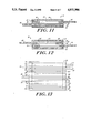
- FIG. 13 is a side view of a multi-terminal chip carrier in accordance with the present invention.
- FIG. 14 is a top view of the chip carrier of FIG. 13 with the lid removed.
- FIG. 15 is a top view of a component of the carrier of FIG. 13.
- FIG. 16 is a cross-sectional view of the chip carrier of FIG. 1 with a power semiconductor device.
- FIG. 1 shows a two terminal chip carrier 10 of the present invention.
- the carrier is formed from a plurality of conductive layers of sheet conductors 20, 24 and an insulating layer 22, such as a ceramic layer.
- a layer 26 is employed to space the layer 24 from a lid 30.
- the layer 26 may be either a conductive or insulating layer as appropriate.
- the lid 30 is the topmost layer.
- the lid may be either an insulator or a conductive material such as KovarTM.
- Carrier 10 is intended for mounting to a circuit board so that the lower surface of conductive layer 20 lies against and contacts the board.
- Conductive layer 24 includes a tab 32 which extends beyond the adjacent insulating layers 22, 24. Tab 32 may be bent down to contact a circuit board.
- Cavity 28, shown in FIGS. 2 and 3, is formed from holes cut through layers 22, 24, and 26.
- one or more semiconductor devices 38 such as a diode, rectifier, darlington, power transistor, or any other power device or integrated circuit may be mounted within cavity 28 and may be connected to the upper surface 34 of conductive layer 28 so that surface 34 forms the bottom of cavity 28.
- the hole through layer 26 is larger than the holes through layers 22 and 24. This larger hole exposes the surface of conductive layer 24, forming a shelf 36 of conductive material.
- a lead 40 from the chip is attached to the shelf 36, by any method well known in the art, to electrically connect the chip to the conductive layer 24.
- Lid 30 is placed over layer 26 to seal the chip within the cavity 28.
- FIG. 4 shows a top view of carrier 10 with lid 30 removed.
- the holes through layers 22 and 24 need not be centered in the layer and may be offset.
- FIGS. 5 and 6 show conductive layer 24 isolated from carrier 10.
- FIGS. 7 and 8 show insulating layer 22 isolated from carrier 10.
- the holes through layers 22 and 24 are of the same size and are aligned when carrier 10 is assembled.
- the layers are each formed from one piece of material, so that no vertical discontinuities are present when carrier 10 is assembled. This insures a continuous periphery surrounding the chip.
- the chip is preferably hermetically sealed within carrier 10 by sealing the layers and lid of carrier 10 together.
- Layers 22, 24 and 26 may be joined together by brazing or any method known in the art.
- Lid 30 may be attached by any known method.
- the layers in the carrier of the present invention are able to expand and contract in response to thermal stresses in a unitary manner, with no significant differential expansions and contractions between the insulating and the conductive layers. Such unitary expansion and contraction allows carrier 10 to maintain a hermetic seal.
- the aforementioned unitary thermal expansion is provided by fabricating the insulating layers and conductive layers from materials with similar or matched coefficients of thermal expansions.
- a suitable insulating material is a ceramic such as alumina.
- a suitable conductive material is a composite material formed from a lamination of copper and molybdenum.
- the layers are formed with a continuous periphery having no vertical discontinuities. This feature further ensures a unitary rather than differential thermal expansion and contraction.
- FIGS. 9 and 10 show an alternative embodiment of carrier 10 of FIG. 1 in which conductive tab 32 of conductive layer 24 is offset to one side allows inversion and reversal of the conductive layer to provide multiple tabs on one side of the carrier.
- FIG. 11 shows an alternative embodiment of the two terminal chip carrier in which the lowest conductive layer 20 includes a conductive tab 42 extending beyond the insulating layer 22. A further insulating layer 44 is placed beneath conductive layer 20. Tab 36 may be bent down to connect to a conductive portion on the circuit board. This embodiment is particularly suitable for attaching to a heat sink when electrical isolation is necessary.
- a three terminal chip carrier 38 is shown in FIG. 12.
- conductive layers 50, 54, and 60 are alternately disposed between the insulating layers 52, 58 and 70.
- Lid 72 may be formed of a material such as KovarTM, and is placed on top of layer 70 to seal the cavity 74.
- Conductive layer 54 has a conductive tab 56 integral with and extending beyond the carrier, and conductive layer 60 likewise has a tab 62 extending beyond the carrier. These tabs may be bent down to contact a circuit board.
- Tabs 56 and 62 are shown extending from opposite sides to carrier 48. Alternatively, the tabs may extend from adjacent sides. Holes are formed through layers 52, 54, 58, 60 and 70, forming cavity 74 for carrying a semiconductor device.
- the hole in insulating layer 58 is cut to expose the upper surface of conductive layer 54, forming shelf 66 to which a lead from the chip may be connected.
- the hole through layer 70 is cut to expose the upper surface of conductive layer 60, forming shelf 68 to which a lead from the chip may be connected.
- FIGS. 13 and 14 show an embodiment of a carrier 80 having eight terminals in addition to a conductive bottom layer.
- the carrier comprises a stack of conductive layers 82, 84, 88, 92, 96, 100, 104, 108 and 112.
- Conductive layer 82 forms the bottom surface 144 of cavity of 142.
- Each conductive layer is separated by insulating layers 120, 122, 124, 126, 128, 130, 132, and 134.
- a seal layer 136 may be formed of an insulating or conductive material as appropriate. Lid 140 is employed to seal the cavity.
- each conductive layer includes a conductive tab 86, 90, 94, 98, 102, 106, 110 and 114, extending from the carrier 80.
- the tabs are best seen in FIG. 14, a top view of carrier 80 with a lid 14 removed.
- Each conductive layer also includes a tab extending into cavity 144 to form a shelf 87, 91, 95, 99, 103, 107, 111, and 115 for providing an area for connecting leads from a semiconductor device disposed in the cavity.
- the shelves are also best seen in FIG. 14.
- FIG. 15 shows single conductive layer 108 isolated from carrier 80.
- Each conductive layer is similarly formed with its tab shelf appropriately positioned in the carrier.
- One or more semiconductor devices may be disposed within the disclosed carrier.
Abstract
Description
Claims (25)
Priority Applications (1)
| Application Number | Priority Date | Filing Date | Title |
|---|---|---|---|
| US07/173,370 US4931906A (en) | 1988-03-25 | 1988-03-25 | Hermetically sealed, surface mountable component and carrier for semiconductor devices |
Applications Claiming Priority (1)
| Application Number | Priority Date | Filing Date | Title |
|---|---|---|---|
| US07/173,370 US4931906A (en) | 1988-03-25 | 1988-03-25 | Hermetically sealed, surface mountable component and carrier for semiconductor devices |
Publications (1)
| Publication Number | Publication Date |
|---|---|
| US4931906A true US4931906A (en) | 1990-06-05 |
Family
ID=22631705
Family Applications (1)
| Application Number | Title | Priority Date | Filing Date |
|---|---|---|---|
| US07/173,370 Expired - Fee Related US4931906A (en) | 1988-03-25 | 1988-03-25 | Hermetically sealed, surface mountable component and carrier for semiconductor devices |
Country Status (1)
| Country | Link |
|---|---|
| US (1) | US4931906A (en) |
Cited By (7)
| Publication number | Priority date | Publication date | Assignee | Title |
|---|---|---|---|---|
| US5031069A (en) * | 1989-12-28 | 1991-07-09 | Sundstrand Corporation | Integration of ceramic capacitor |
| US5128749A (en) * | 1991-04-08 | 1992-07-07 | Grumman Aerospace Corporation | Fused high density multi-layer integrated circuit module |
| US5225897A (en) * | 1991-10-02 | 1993-07-06 | Unitrode Corporation | Molded package for semiconductor devices with leadframe locking structure |
| US5401688A (en) * | 1991-02-18 | 1995-03-28 | Kabushiki Kaisha Toshiba | Semiconductor device of multichip module-type |
| US5856235A (en) * | 1995-04-12 | 1999-01-05 | Northrop Grumman Corporation | Process of vacuum annealing a thin film metallization on high purity alumina |
| US20060043550A1 (en) * | 2004-08-25 | 2006-03-02 | International Rectifier Corporation | Hermetic semiconductor package |
| US11749533B2 (en) * | 2020-04-21 | 2023-09-05 | Fraunhofer-Gesellschaft zur Förderung der angewandten Forschung e.V. | Method of manufacturing a power semiconductor component arrangement or a power semiconductor component housing |
Citations (19)
| Publication number | Priority date | Publication date | Assignee | Title |
|---|---|---|---|---|
| US3777220A (en) * | 1972-06-30 | 1973-12-04 | Ibm | Circuit panel and method of construction |
| US3959874A (en) * | 1974-12-20 | 1976-06-01 | Western Electric Company, Inc. | Method of forming an integrated circuit assembly |
| US3961415A (en) * | 1975-01-02 | 1976-06-08 | Hughes Aircraft Company | Carrier for mounting a semiconductor chip and method therefor |
| US4162514A (en) * | 1976-10-27 | 1979-07-24 | Bbc Brown, Boveri & Company, Limited | Arrangement for semiconductor power components |
| US4246596A (en) * | 1978-01-07 | 1981-01-20 | Tokyo Shibaura Denki Kabushiki Kaisha | High current press pack semiconductor device having a mesa structure |
| US4250482A (en) * | 1979-01-02 | 1981-02-10 | Allen-Bradley Company | Packaged electronic component and method of preparing the same |
| US4355463A (en) * | 1980-03-24 | 1982-10-26 | National Semiconductor Corporation | Process for hermetically encapsulating semiconductor devices |
| US4474292A (en) * | 1980-05-20 | 1984-10-02 | Gao Gesellschaft Fur Automation Und Organisation Mbh | Carrier element for an IC-chip |
| US4538170A (en) * | 1983-01-03 | 1985-08-27 | General Electric Company | Power chip package |
| US4581479A (en) * | 1984-11-16 | 1986-04-08 | Moore Theodore W | Dimensionally precise electronic component mount |
| US4594644A (en) * | 1984-10-22 | 1986-06-10 | Electronic Instrument & Specialty Corp. | Electrical component encapsulation package |
| US4595096A (en) * | 1981-02-09 | 1986-06-17 | British Telecommunications | Integrated circuit chip carrier |
| US4630172A (en) * | 1983-03-09 | 1986-12-16 | Printed Circuits International | Semiconductor chip carrier package with a heat sink |
| US4677741A (en) * | 1981-11-30 | 1987-07-07 | Mitsubishi Denki Kabushiki Kaisha | Method of manufacturing package for high power integrated circuit |
| US4692789A (en) * | 1982-07-23 | 1987-09-08 | Kabushiki Kaisha Toyota Chuo Kenkyusho | Semiconductor apparatus |
| US4729061A (en) * | 1985-04-29 | 1988-03-01 | Advanced Micro Devices, Inc. | Chip on board package for integrated circuit devices using printed circuit boards and means for conveying the heat to the opposite side of the package from the chip mounting side to permit the heat to dissipate therefrom |
| US4731701A (en) * | 1987-05-12 | 1988-03-15 | Fairchild Semiconductor Corporation | Integrated circuit package with thermal path layers incorporating staggered thermal vias |
| US4750089A (en) * | 1985-11-22 | 1988-06-07 | Texas Instruments Incorporated | Circuit board with a chip carrier and mounting structure connected to the chip carrier |
| US4812792A (en) * | 1983-12-22 | 1989-03-14 | Trw Inc. | High-frequency multilayer printed circuit board |
-
1988
- 1988-03-25 US US07/173,370 patent/US4931906A/en not_active Expired - Fee Related
Patent Citations (19)
| Publication number | Priority date | Publication date | Assignee | Title |
|---|---|---|---|---|
| US3777220A (en) * | 1972-06-30 | 1973-12-04 | Ibm | Circuit panel and method of construction |
| US3959874A (en) * | 1974-12-20 | 1976-06-01 | Western Electric Company, Inc. | Method of forming an integrated circuit assembly |
| US3961415A (en) * | 1975-01-02 | 1976-06-08 | Hughes Aircraft Company | Carrier for mounting a semiconductor chip and method therefor |
| US4162514A (en) * | 1976-10-27 | 1979-07-24 | Bbc Brown, Boveri & Company, Limited | Arrangement for semiconductor power components |
| US4246596A (en) * | 1978-01-07 | 1981-01-20 | Tokyo Shibaura Denki Kabushiki Kaisha | High current press pack semiconductor device having a mesa structure |
| US4250482A (en) * | 1979-01-02 | 1981-02-10 | Allen-Bradley Company | Packaged electronic component and method of preparing the same |
| US4355463A (en) * | 1980-03-24 | 1982-10-26 | National Semiconductor Corporation | Process for hermetically encapsulating semiconductor devices |
| US4474292A (en) * | 1980-05-20 | 1984-10-02 | Gao Gesellschaft Fur Automation Und Organisation Mbh | Carrier element for an IC-chip |
| US4595096A (en) * | 1981-02-09 | 1986-06-17 | British Telecommunications | Integrated circuit chip carrier |
| US4677741A (en) * | 1981-11-30 | 1987-07-07 | Mitsubishi Denki Kabushiki Kaisha | Method of manufacturing package for high power integrated circuit |
| US4692789A (en) * | 1982-07-23 | 1987-09-08 | Kabushiki Kaisha Toyota Chuo Kenkyusho | Semiconductor apparatus |
| US4538170A (en) * | 1983-01-03 | 1985-08-27 | General Electric Company | Power chip package |
| US4630172A (en) * | 1983-03-09 | 1986-12-16 | Printed Circuits International | Semiconductor chip carrier package with a heat sink |
| US4812792A (en) * | 1983-12-22 | 1989-03-14 | Trw Inc. | High-frequency multilayer printed circuit board |
| US4594644A (en) * | 1984-10-22 | 1986-06-10 | Electronic Instrument & Specialty Corp. | Electrical component encapsulation package |
| US4581479A (en) * | 1984-11-16 | 1986-04-08 | Moore Theodore W | Dimensionally precise electronic component mount |
| US4729061A (en) * | 1985-04-29 | 1988-03-01 | Advanced Micro Devices, Inc. | Chip on board package for integrated circuit devices using printed circuit boards and means for conveying the heat to the opposite side of the package from the chip mounting side to permit the heat to dissipate therefrom |
| US4750089A (en) * | 1985-11-22 | 1988-06-07 | Texas Instruments Incorporated | Circuit board with a chip carrier and mounting structure connected to the chip carrier |
| US4731701A (en) * | 1987-05-12 | 1988-03-15 | Fairchild Semiconductor Corporation | Integrated circuit package with thermal path layers incorporating staggered thermal vias |
Cited By (8)
| Publication number | Priority date | Publication date | Assignee | Title |
|---|---|---|---|---|
| US5031069A (en) * | 1989-12-28 | 1991-07-09 | Sundstrand Corporation | Integration of ceramic capacitor |
| US5401688A (en) * | 1991-02-18 | 1995-03-28 | Kabushiki Kaisha Toshiba | Semiconductor device of multichip module-type |
| US5128749A (en) * | 1991-04-08 | 1992-07-07 | Grumman Aerospace Corporation | Fused high density multi-layer integrated circuit module |
| US5225897A (en) * | 1991-10-02 | 1993-07-06 | Unitrode Corporation | Molded package for semiconductor devices with leadframe locking structure |
| US5856235A (en) * | 1995-04-12 | 1999-01-05 | Northrop Grumman Corporation | Process of vacuum annealing a thin film metallization on high purity alumina |
| US20060043550A1 (en) * | 2004-08-25 | 2006-03-02 | International Rectifier Corporation | Hermetic semiconductor package |
| US8232635B2 (en) | 2004-08-25 | 2012-07-31 | International Rectifier Corporation | Hermetic semiconductor package |
| US11749533B2 (en) * | 2020-04-21 | 2023-09-05 | Fraunhofer-Gesellschaft zur Förderung der angewandten Forschung e.V. | Method of manufacturing a power semiconductor component arrangement or a power semiconductor component housing |
Similar Documents
| Publication | Publication Date | Title |
|---|---|---|
| US5563446A (en) | Surface mount peripheral leaded and ball grid array package | |
| JP4275783B2 (en) | Power semiconductor module | |
| US4763188A (en) | Packaging system for multiple semiconductor devices | |
| US4907067A (en) | Thermally efficient power device package | |
| US7880283B2 (en) | High reliability power module | |
| US4103318A (en) | Electronic multichip module | |
| US4783697A (en) | Leadless chip carrier for RF power transistors or the like | |
| US5075759A (en) | Surface mounting semiconductor device and method | |
| JP2724312B2 (en) | IC chip carrier package | |
| US4755910A (en) | Housing for encapsulating an electronic circuit | |
| KR100328143B1 (en) | Lead frame with layered conductive plane | |
| US4167647A (en) | Hybrid microelectronic circuit package | |
| EP0488783A2 (en) | Lead frame for semiconductor device comprising a heat sink | |
| US20070273009A1 (en) | Highly efficient both-side-cooled discrete power package, especially basic element for innovative power modules | |
| US4642419A (en) | Four-leaded dual in-line package module for semiconductor devices | |
| US4961107A (en) | Electrically isolated heatsink for single-in-line package | |
| US6157076A (en) | Hermetic thin pack semiconductor device | |
| KR960012647B1 (en) | Semiconductor device and manufacture method | |
| US4885662A (en) | Circuit module connection system | |
| WO2003060984A1 (en) | Surface mounted package with die bottom spaced from support board | |
| JPH1174454A (en) | Power semiconductor module containing encapsulated submodules | |
| US4931906A (en) | Hermetically sealed, surface mountable component and carrier for semiconductor devices | |
| US6049971A (en) | Casing for integrated circuit chips and method of fabrication | |
| US7229855B2 (en) | Process for assembling a double-sided circuit component | |
| EP0924845A2 (en) | Power semiconductor module |
Legal Events
| Date | Code | Title | Description |
|---|---|---|---|
| AS | Assignment |
Owner name: UNITRODE CORPORATION, 5 FORBES ROAD, LEXINGTON, MA Free format text: ASSIGNMENT OF ASSIGNORS INTEREST.;ASSIGNORS:REIFEL, HARRY C.;ERDAG, EREN;SOEREWYN, HERMAN VAN DYK;REEL/FRAME:004927/0887 Effective date: 19880414 Owner name: UNITRODE CORPORATION, A MASSACHUSETTS CORP., MASSA Free format text: ASSIGNMENT OF ASSIGNORS INTEREST;ASSIGNORS:REIFEL, HARRY C.;ERDAG, EREN;SOEREWYN, HERMAN VAN DYK;REEL/FRAME:004927/0887 Effective date: 19880414 |
|
| CC | Certificate of correction | ||
| FEPP | Fee payment procedure |
Free format text: PAYOR NUMBER ASSIGNED (ORIGINAL EVENT CODE: ASPN); ENTITY STATUS OF PATENT OWNER: LARGE ENTITY |
|
| AS | Assignment |
Owner name: MICRO USPD, INC., MASSACHUSETTS Free format text: ASSIGNMENT OF ASSIGNORS INTEREST;ASSIGNOR:UNITRODE CORPORATION;REEL/FRAME:006608/0819 Effective date: 19920702 |
|
| FPAY | Fee payment |
Year of fee payment: 4 |
|
| REMI | Maintenance fee reminder mailed | ||
| LAPS | Lapse for failure to pay maintenance fees | ||
| FP | Lapsed due to failure to pay maintenance fee |
Effective date: 19980610 |
|
| STCH | Information on status: patent discontinuation |
Free format text: PATENT EXPIRED DUE TO NONPAYMENT OF MAINTENANCE FEES UNDER 37 CFR 1.362 |