US4930107A - Method and apparatus for programming and verifying programmable elements in programmable devices - Google Patents
Method and apparatus for programming and verifying programmable elements in programmable devices Download PDFInfo
- Publication number
- US4930107A US4930107A US07/229,852 US22985288A US4930107A US 4930107 A US4930107 A US 4930107A US 22985288 A US22985288 A US 22985288A US 4930107 A US4930107 A US 4930107A
- Authority
- US
- United States
- Prior art keywords
- programming
- shift registers
- address information
- programmable
- array
- Prior art date
- Legal status (The legal status is an assumption and is not a legal conclusion. Google has not performed a legal analysis and makes no representation as to the accuracy of the status listed.)
- Expired - Lifetime
Links
Images


Classifications
-
- H—ELECTRICITY
- H03—ELECTRONIC CIRCUITRY
- H03K—PULSE TECHNIQUE
- H03K19/00—Logic circuits, i.e. having at least two inputs acting on one output; Inverting circuits
- H03K19/02—Logic circuits, i.e. having at least two inputs acting on one output; Inverting circuits using specified components
- H03K19/173—Logic circuits, i.e. having at least two inputs acting on one output; Inverting circuits using specified components using elementary logic circuits as components
- H03K19/177—Logic circuits, i.e. having at least two inputs acting on one output; Inverting circuits using specified components using elementary logic circuits as components arranged in matrix form
- H03K19/17704—Logic circuits, i.e. having at least two inputs acting on one output; Inverting circuits using specified components using elementary logic circuits as components arranged in matrix form the logic functions being realised by the interconnection of rows and columns
- H03K19/17708—Logic circuits, i.e. having at least two inputs acting on one output; Inverting circuits using specified components using elementary logic circuits as components arranged in matrix form the logic functions being realised by the interconnection of rows and columns using an AND matrix followed by an OR matrix, i.e. programmable logic arrays
- H03K19/17712—Logic circuits, i.e. having at least two inputs acting on one output; Inverting circuits using specified components using elementary logic circuits as components arranged in matrix form the logic functions being realised by the interconnection of rows and columns using an AND matrix followed by an OR matrix, i.e. programmable logic arrays one of the matrices at least being reprogrammable
Definitions
- Programmable logic devices of the types described generally in Spencer U.S. Pat. No. 3,566,153, Birkner et al. U.S. Pat. No. 4,124,899, Hartmann et al. U.S. Pat. No. 4,609,986, Hartmann et al. U.S. Pat. No. 4,617,479 and Hartmann et al. U.S. Pat. No. 4,713,792 can be implemented using fuses, anti-fuses, erasable programmable read-only memory (EPROM), electrically erasable programmable read-only memory (EEPROM) or flash EPROM as their programmable elements.
- EPROM erasable programmable read-only memory
- EEPROM electrically erasable programmable read-only memory
- flash EPROM flash EPROM
- Such devices are typically set up as basically orthogonal arrays of "bit lines” and “word lines” which can be programmably interconnected to achieve a desired logical result. It is known that the programmable interconnections in such devices can be programmed by addressing the appropriate bit lines and word lines, applying the desired programming data, and transferring that data to the interconnection by applying to the selected word lines and bit lines a predetermined programming voltage--e.g., a voltage significantly higher than that encountered in the normal logical operation of the device.
- a predetermined programming voltage--e.g., a voltage significantly higher than that encountered in the normal logical operation of the device e.g., a voltage significantly higher than that encountered in the normal logical operation of the device.
- a programmable array is generally organized as an array of m ⁇ n programmable elements.
- n EPROM gates to each of the m word lines are connected n EPROM gates, and to each of the n bit lines are connected m EPROM drains.
- any bit at the intersection of a high voltage bit line and a high voltage word line will be programmed.
- the address information for the word lines and bit lines is binarily encoded.
- log 2 m address lines for the word lines and log 2 n address lines for the bit lines each rounded up to the nearest whole number, are required.
- the total number of lines to address all interconnections uniquely is the sum of log 2 m rounded up to the nearest whole number and log 2 n rounded to the nearest whole number.
- each decoder in terms of numbers of input lines and numbers of decoded output lines for each array block. Furthermore, it is generally prudent to physically place each decoder close to its associated array block to avoid to having to route the decoded lines across long distances across the chip. However, areas close to some of the arrays may be needed for other circuit functions during normal operation of the chip. These limitations may present difficulty for the integrated circuit designer in trading off the use of limited silicon area for signal lines and decoders for programming of the programmable elements on the one hand, and implementing other circuits necessary for the performance of intended logic functions during the normal operation of the chip on the other hand.
- apparatus for programming a programmable logic array having at least m word lines, at least n bit lines, and at least m ⁇ n programmable interconnections.
- the apparatus includes means for applying programming data to the array and means for providing serial address information to the array for indicating for which of the programmable interconnections the programming data is intended.
- a programming method is also provided.
- FIG. 1 is a schematic representation of an EPROM transistor used as a programmable interconnection element in programmable logic devices implemented with EPROM;
- FIG. 2 is a cross-sectional view of the EPROM transistor of FIG. 1;
- FIGS. 3A and 3B are a schematic representation of a known type of programming circuit for programmable logic devices
- FIGS. 4A to 4C are a schematic representation of a programming circuit according to this invention for use with a programmable logic device.
- FIGS. 5A to 5F are a schematic representation of a programming circuit according to this invention for use with more than one programmable logic device.
- an EPROM element such as a floating gate field effect transistor 10, shown in FIGS. 1 and 2, commonly referred to as an EPROM transistor, is programmed when the voltage on its control gate 11 is at a voltage (e.g., 12 volts) that is significantly higher than the voltage during normal operation (typically 5 volts) and the voltage at the drain 12 of EPROM element 10 is at a voltage (e.g., 10-12 volts) higher than the voltage during normal operation (e.g., 5 volts).
- a voltage e.g., 12 volts
- the voltage at the drain 12 of EPROM element 10 is at a voltage (e.g., 10-12 volts) higher than the voltage during normal operation (e.g., 5 volts).
- the number of address input lines to the bit lines can be reduced by programming the arrays one byte (eight bits) at a time in parallel, with the programming information coming into eight-bit column driver 36 via D0-D7 address pins 37.
- seven input lines (four word line address inputs 34 and three bit line address inputs 35) have to be reserved or multiplexed to be used as address input lines.
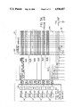
- FIG. 4 shows a programming circuit according to the present invention as applied to a single EPROM array 41 consisting of ten word lines 32 and fifty-six bit lines 33. Each intersection of bit line and word line consists of an EPROM element 10 with its gate 11 connected to a word line 32 and its drain 12 connected to a bit line 33.
- Programming circuit 40 according to the invention is shown as being associated with array 41. No additional pins are added to the programmable integrated circuit device in order to accommodate programming circuit 40. Instead, pins which during normal operation of the chip perform functions related to data input/output, and input signal pins, will perform programming functions once the chip is placed in the programming mode.
- the chip is placed in a programming mode by applying to a programming control pin (not shown) the extra-high voltage (typically 12 volts) referred to above.
- a second programming control pin (also not shown) is held in a logical low state (0 volt) during programming.
- Programming circuit 40 can also perform verification functions. To place the chip into a verification mode, the extra high voltage is applied to the second programming control pin as well.
- the manner in which EPROM cells 10 are addressed is the same, except that in programming mode, data to be programmed are inputted through the input path of data input/output lines of array 41 and translated to extra-high voltage levels on bit lines 33, and in verification mode, data from array 41 is read out through the output path of data input/output lines of array 41.
- programming data is supplied to the array one byte (eight bits) at a time, from D0-D7 data input/output pins 37 through eight-bit column driver 36.
- first level bit line shift register block 60 selects the particular bit lines
- first level word line shift register block 70 selects the particular word lines, of array 41 that are activated.
- a logical "1" is shifted into shift register 600 from pin 42 by a clock input to pin 43 in register block 60
- a logical "1" is shifted into shift register 700 from pin 44 by a clock input to pin 45 in register block 70.
- the first level shift register blocks 60, 70 serve the purpose of selecting a particular array, or part thereof, for an integrated circuit with more than one programmable array, or a single large programmable array.
- the function of the first level shift registers will be clearer when considered in connection with programmable logic having a plurality of programmable arrays of possibly different dimensions, as discussed in more detail below in connection with FIG. 5.
- the desired word line is addressed by clocking a logical "1" into shift registers 200 on line 48, controlled by a clock signal on line 49. This causes a logical "1” to be placed on the output of the shift register corresponding to the particular word line selected.
- a logical "1” is clocked into shift register 500 on line 46, controlled by a clock signal on line 47. After the correct number of clock pulses from lines 49 and 47, logical "1's" will have been placed on the output of shift registers 200 and 500 corresponding to selected word lines and bit lines.
- first level registers 600, 700 of blocks 60, 70 each at a logical "1"
- the AND gates 300 for bit line drivers 303 and word line drivers 302 are enabled.
- the logical "1" outputs of AND gates 300 are at extra-high voltage (e.g., 12 volts) in the programming mode and at regular logical "1" voltage (e.g., 5 volts) in the verification mode.
- the programming data for the programmable interconnection being accessed will have been applied via D0-D7 data lines 37 to eight-bit column driver 36 connected to array 41 through lines 370-377.
- a logical "1" on shift register 500 turns on one of the N-channel MOS transistors 410 in each of blocks 400 through 407 allowing the extra-high voltage from eight-bit column driver 36 to be delivered selectively to particular bit lines of array 41.
- the programmed pattern on the array can be verified by entering the verification mode as described previously, in which case programmed bit pattern information may be read out on D0-D7 lines 37 in parallel format.
- first level shift register blocks 60, 70, nor pins 42-45 For a single array, it is not necessary to have first level shift register blocks 60, 70, nor pins 42-45.
- serial addressing scheme shown the addressing of a single array of any dimensions requires only four input signal pins 46-49. Because clock pins 47 and 49 are two independent clocks, logical "1's" can be shifted into shift register blocks 50 and 20 at the same time. If one wishes to shift in a logical "1" into shift register block 50 before or after shifting a logical "1" into shift register block 20, then the data input pins 46, 48 can be common and combined into a single data input pin.
- the addressing of a single array of any dimensions requires a minimum of only three input signal pins 47, 49 and 46 or 48, compared to the seven address input lines required even with the small array described in FIG. 3 using a conventional addressing scheme.
- a pin 304 normally used for other signal output purposes, is used as shift register output monitor. Data from each block of shift registers can be clocked out on a per block basis, with clocks from other shift register blocks stopped so that three of the inputs to the OR gate 52 are at a logical "0". By counting the number of clock pulses before a logical "1" is detected on pin 304, the position and operation of the shift registers can be determined for the block being monitored.
- FIG. 5 shows an embodiment of the serial addressing circuit of the invention in a programmable integrated circuit having ten programmable arrays.
- Eight arrays 41, 411-417 are of the same structure as in FIG. 4, each having ten word lines and fifty-six bit lines.
- Array 120 is a programmable array having seventy-two word lines and eighty-eight bit lines.
- Array 130 has eighteen word lines and fifty-six bit lines. Programming data for all of the arrays are supplied from D0-D7 lines 37 through high voltage eight-bit column driver 36 as described above for the case of a single array.
- the internal data lines 370-377 are common to all arrays.
- the seventy-two word lines of array 120 are controlled by eight groups of word line drivers 121, each containing nine two-input AND gate word line drivers 300 as in block 302 of FIG. 4.
- the common inputs of each block of AND gates are controlled by shift registers 708-715 of block 70.
- Shift registers 708-715 of block 70 can select any one of eight word line driver blocks 121 by shifting a logical "1" to the appropriate shift register output by clocking pin 45. By shifting a logical "1" into the appropriate shift register 200 in block 20, one out of the nine word line drivers in each block 121 can be selected.
- shift register block 20 can also select the word lines of any of arrays 41, 411-417.
- Programming data for the eighty-eight bit lines of array 120 are applied through D0-D7 lines 37, and eight-bit column driver 36, eight bits at a time in parallel.
- the number of shift registers does not grow directy as the number lines on the integrated circuit chip 550 to be selected. Rather, the number of shift registers at most equals the number of lines to be selected in the largest one of the several programmable arrays on the integrated circuit chip.
- pins 42, 44, 46 and 48 can be combined into one data input pin if one is willing to shift the logical "1's" into shift register blocks 600-609, 700-717, 50-51, 20 one block after another in the same manner as described for the single array of FIG. 4.
- the total number of input pins then required will be reduced from eight to only five (43, 45, 47, 49 and 42 or 44 or 46 or 48) by combining pins 42, 44, 46 and 48 into one pin.
- data pins 42, 44, 46, 48 can remain independent and clock pins 43, 45, 47, 49 can be combined.
- the programming circuit of chip 550 in FIG. 5 serially addresses the programmable interconnections to be programmed in each of arrays 120, 130, 41, 411-417.
- serial addressing only five (for a 2-level shift register scheme), and as few as three (for a single level shift register scheme), programming address lines need to be brought from input pins of chip 550 to the arrays to be programmed, reducing the number of input pins required on the chip for programming and verification.
- the number of shift registers can be further reduced as compared to direct addressing, because on a chip with multiple programmable arrays or large arrays, the same shift registers can be used for all arrays, even those of different sizes, and for the different parts of the large arrays if they are programmed in parts.
- serial addressing is that by shifting more than one logical "1" into the shift register chain, any chosen number of lines can be selected simultaneously. Applications of multiple selections include programming of the array more than a byte at a time to save programming time. During reliability testing of the programmable arrays, it may be desirable to stress the programmable elements in such a way that all word lines are at logical "1's" and all bit lines are at logic "0". Serial addressing as described allows such addressing without any additional circuits.
Abstract
Description
Claims (24)
Priority Applications (3)
| Application Number | Priority Date | Filing Date | Title |
|---|---|---|---|
| US07/229,852 US4930107A (en) | 1988-08-08 | 1988-08-08 | Method and apparatus for programming and verifying programmable elements in programmable devices |
| EP19890306841 EP0354658A3 (en) | 1988-08-08 | 1989-07-05 | Method and apparatus for programming and verifying programmable elements in programmable devices |
| JP1198108A JPH02168499A (en) | 1988-08-08 | 1989-08-01 | Method and apparatus for programming and |
Applications Claiming Priority (1)
| Application Number | Priority Date | Filing Date | Title |
|---|---|---|---|
| US07/229,852 US4930107A (en) | 1988-08-08 | 1988-08-08 | Method and apparatus for programming and verifying programmable elements in programmable devices |
Publications (1)
| Publication Number | Publication Date |
|---|---|
| US4930107A true US4930107A (en) | 1990-05-29 |
Family
ID=22862929
Family Applications (1)
| Application Number | Title | Priority Date | Filing Date |
|---|---|---|---|
| US07/229,852 Expired - Lifetime US4930107A (en) | 1988-08-08 | 1988-08-08 | Method and apparatus for programming and verifying programmable elements in programmable devices |
Country Status (3)
| Country | Link |
|---|---|
| US (1) | US4930107A (en) |
| EP (1) | EP0354658A3 (en) |
| JP (1) | JPH02168499A (en) |
Cited By (19)
| Publication number | Priority date | Publication date | Assignee | Title |
|---|---|---|---|---|
| WO1994010754A1 (en) * | 1992-11-05 | 1994-05-11 | Xilinx, Inc. | Improved configurable cellular array |
| US5493239A (en) * | 1995-01-31 | 1996-02-20 | Motorola, Inc. | Circuit and method of configuring a field programmable gate array |
| US5510730A (en) | 1986-09-19 | 1996-04-23 | Actel Corporation | Reconfigurable programmable interconnect architecture |
| US5521833A (en) * | 1991-11-28 | 1996-05-28 | Siemens Aktiengesellschaft | Method for programming programmable integrated circuits |
| US5555214A (en) * | 1995-11-08 | 1996-09-10 | Altera Corporation | Apparatus for serial reading and writing of random access memory arrays |
| US5680061A (en) * | 1995-05-17 | 1997-10-21 | Altera Corporation | Techniques for programming programmable logic array devices |
| US5796750A (en) * | 1994-04-22 | 1998-08-18 | Lattice Semiconductor Corporation | Method for programming a programmable logic device in an automatic tester |
| US5838584A (en) * | 1995-01-27 | 1998-11-17 | Altera Corporation | Optimizing chain placement in a programmable logic device |
| US6181598B1 (en) * | 1992-03-17 | 2001-01-30 | Hitachi, Ltd. | Data line disturbance free memory block divided flash memory and microcomputer having flash memory |
| US6310809B1 (en) * | 2000-08-25 | 2001-10-30 | Micron Technology, Inc. | Adjustable pre-charge in a memory |
| US6384630B2 (en) | 1996-06-05 | 2002-05-07 | Altera Corporation | Techniques for programming programmable logic array devices |
| US6414878B2 (en) | 1992-03-17 | 2002-07-02 | Hitachi, Ltd. | Data line disturbance free memory block divided flash memory and microcomputer having flash memory therein |
| US20030097628A1 (en) * | 2001-10-11 | 2003-05-22 | Ngo Ninh D. | Error detection on programmable logic resources |
| US6714044B1 (en) | 2002-03-25 | 2004-03-30 | Altera Corporation | Hi-speed parallel configuration of programmable logic |
| US6766505B1 (en) | 2002-03-25 | 2004-07-20 | Altera Corporation | Parallel programming of programmable logic using register chains |
| US20060050568A1 (en) * | 2004-09-08 | 2006-03-09 | Kao Oliver C | Programmable logic auto write-back |
| US7328377B1 (en) | 2004-01-27 | 2008-02-05 | Altera Corporation | Error correction for programmable logic integrated circuits |
| US7343470B1 (en) | 2003-09-26 | 2008-03-11 | Altera Corporation | Techniques for sequentially transferring data from a memory device through a parallel interface |
| US20100302293A1 (en) * | 2007-11-14 | 2010-12-02 | Torgerson Joseph M | Inkjet print head with shared data lines |
Citations (8)
| Publication number | Priority date | Publication date | Assignee | Title |
|---|---|---|---|---|
| US3566153A (en) * | 1969-04-30 | 1971-02-23 | Texas Instruments Inc | Programmable sequential logic |
| US4124899A (en) * | 1977-05-23 | 1978-11-07 | Monolithic Memories, Inc. | Programmable array logic circuit |
| US4347587A (en) * | 1979-11-23 | 1982-08-31 | Texas Instruments Incorporated | Semiconductor integrated circuit memory device with both serial and random access arrays |
| US4524430A (en) * | 1983-01-11 | 1985-06-18 | Burroughs Corporation | Dynamic data re-programmable PLA |
| US4609986A (en) * | 1984-06-14 | 1986-09-02 | Altera Corporation | Programmable logic array device using EPROM technology |
| US4617479A (en) * | 1984-05-03 | 1986-10-14 | Altera Corporation | Programmable logic array device using EPROM technology |
| US4713792A (en) * | 1985-06-06 | 1987-12-15 | Altera Corporation | Programmable macrocell using eprom or eeprom transistors for architecture control in programmable logic circuits |
| US4761768A (en) * | 1985-03-04 | 1988-08-02 | Lattice Semiconductor Corporation | Programmable logic device |
Family Cites Families (1)
| Publication number | Priority date | Publication date | Assignee | Title |
|---|---|---|---|---|
| US4766569A (en) * | 1985-03-04 | 1988-08-23 | Lattice Semiconductor Corporation | Programmable logic array |
-
1988
- 1988-08-08 US US07/229,852 patent/US4930107A/en not_active Expired - Lifetime
-
1989
- 1989-07-05 EP EP19890306841 patent/EP0354658A3/en not_active Ceased
- 1989-08-01 JP JP1198108A patent/JPH02168499A/en active Pending
Patent Citations (10)
| Publication number | Priority date | Publication date | Assignee | Title |
|---|---|---|---|---|
| US3566153A (en) * | 1969-04-30 | 1971-02-23 | Texas Instruments Inc | Programmable sequential logic |
| US4124899A (en) * | 1977-05-23 | 1978-11-07 | Monolithic Memories, Inc. | Programmable array logic circuit |
| US4124899B1 (en) * | 1977-05-23 | 1987-04-28 | ||
| US4347587A (en) * | 1979-11-23 | 1982-08-31 | Texas Instruments Incorporated | Semiconductor integrated circuit memory device with both serial and random access arrays |
| US4524430A (en) * | 1983-01-11 | 1985-06-18 | Burroughs Corporation | Dynamic data re-programmable PLA |
| US4617479A (en) * | 1984-05-03 | 1986-10-14 | Altera Corporation | Programmable logic array device using EPROM technology |
| US4617479B1 (en) * | 1984-05-03 | 1993-09-21 | Altera Semiconductor Corp. | Programmable logic array device using eprom technology |
| US4609986A (en) * | 1984-06-14 | 1986-09-02 | Altera Corporation | Programmable logic array device using EPROM technology |
| US4761768A (en) * | 1985-03-04 | 1988-08-02 | Lattice Semiconductor Corporation | Programmable logic device |
| US4713792A (en) * | 1985-06-06 | 1987-12-15 | Altera Corporation | Programmable macrocell using eprom or eeprom transistors for architecture control in programmable logic circuits |
Cited By (51)
| Publication number | Priority date | Publication date | Assignee | Title |
|---|---|---|---|---|
| US5510730A (en) | 1986-09-19 | 1996-04-23 | Actel Corporation | Reconfigurable programmable interconnect architecture |
| US6160420A (en) | 1986-09-19 | 2000-12-12 | Actel Corporation | Programmable interconnect architecture |
| US5521833A (en) * | 1991-11-28 | 1996-05-28 | Siemens Aktiengesellschaft | Method for programming programmable integrated circuits |
| US7295476B2 (en) | 1992-03-17 | 2007-11-13 | Renesas Technology Corp. | Data line disturbance free memory block divided flash memory and microcomputer having flash memory therein |
| US6335879B1 (en) | 1992-03-17 | 2002-01-01 | Hitachi, Ltd. | Method of erasing and programming a flash memory in a single-chip microcomputer having a processing unit and memory |
| US7965563B2 (en) | 1992-03-17 | 2011-06-21 | Renesas Technology Corp. | Data line disturbance free memory block divided flash memory and microcomputer having flash memory therein |
| US7505329B2 (en) | 1992-03-17 | 2009-03-17 | Renesas Technology Corp. | Data line disturbance free memory block divided flash memory and microcomputer having flash memory therein |
| US6690603B2 (en) | 1992-03-17 | 2004-02-10 | Hitachi, Ltd. | Microcomputer including a flash memory that is two-way programmable |
| US20060034129A1 (en) * | 1992-03-17 | 2006-02-16 | Kiyoshi Matsubara | Data line disturbance free memory block divided flash memory and microcomputer having flash memory therein |
| US6999350B2 (en) | 1992-03-17 | 2006-02-14 | Renesas Technology Corp. | Data line disturbance free memory block divided flash memory and microcomputer having flash memory therein |
| US20040268025A1 (en) * | 1992-03-17 | 2004-12-30 | Kiyoshi Matsubara | Data line disturbance free memory block divided flash memory and microcomputer having flash memory therein |
| US6804152B2 (en) | 1992-03-17 | 2004-10-12 | Renesas Technology Corp. | Method for manufacturing a printed board on which a semiconductor device having two modes is mounted |
| US7184321B2 (en) | 1992-03-17 | 2007-02-27 | Hitachi Ulsi Systems Co., Ltd. | Data line disturbance free memory block divided flash memory and microcomputer having flash memory therein |
| US6493271B2 (en) | 1992-03-17 | 2002-12-10 | Hitachi, Ltd. | Data line disturbance free memory block divided flash memory and microcomputer having flash memory therein |
| US6414878B2 (en) | 1992-03-17 | 2002-07-02 | Hitachi, Ltd. | Data line disturbance free memory block divided flash memory and microcomputer having flash memory therein |
| US6181598B1 (en) * | 1992-03-17 | 2001-01-30 | Hitachi, Ltd. | Data line disturbance free memory block divided flash memory and microcomputer having flash memory |
| US6400609B1 (en) | 1992-03-17 | 2002-06-04 | Hitachi, Ltd. | Data line disturbance free memory block divided flash memory and microcomputer having flash memory therein |
| US20030021157A1 (en) * | 1992-03-17 | 2003-01-30 | Kiyoshi Matsubara | Data line disturbance free memory block divided flash memory and microcomputer having flash memory therein |
| WO1994010754A1 (en) * | 1992-11-05 | 1994-05-11 | Xilinx, Inc. | Improved configurable cellular array |
| US6292018B1 (en) * | 1992-11-05 | 2001-09-18 | Xilinx, Inc. | Configurable cellular array |
| US5528176A (en) * | 1992-11-05 | 1996-06-18 | Xilinx, Inc. | Register with duplicate decoders for configurable cellular array |
| US5469003A (en) * | 1992-11-05 | 1995-11-21 | Xilinx, Inc. | Hierarchically connectable configurable cellular array |
| US5552722A (en) * | 1992-11-05 | 1996-09-03 | Xilinx, Inc. | Mask registor for a configurable cellular array |
| US5831448A (en) * | 1992-11-05 | 1998-11-03 | Xilinx, Inc. | Function unit for fine-gained FPGA |
| US5670897A (en) * | 1992-11-05 | 1997-09-23 | Xilinx, Inc. | High speed mask register for a configurable cellular array |
| US5798656A (en) * | 1992-11-05 | 1998-08-25 | Xilinx, Inc. | Match register with duplicate decoders |
| US5796750A (en) * | 1994-04-22 | 1998-08-18 | Lattice Semiconductor Corporation | Method for programming a programmable logic device in an automatic tester |
| US5838584A (en) * | 1995-01-27 | 1998-11-17 | Altera Corporation | Optimizing chain placement in a programmable logic device |
| US5493239A (en) * | 1995-01-31 | 1996-02-20 | Motorola, Inc. | Circuit and method of configuring a field programmable gate array |
| US6184705B1 (en) | 1995-05-17 | 2001-02-06 | Altera Corporation | Techniques for programming programmable logic array devices |
| US5680061A (en) * | 1995-05-17 | 1997-10-21 | Altera Corporation | Techniques for programming programmable logic array devices |
| US5555214A (en) * | 1995-11-08 | 1996-09-10 | Altera Corporation | Apparatus for serial reading and writing of random access memory arrays |
| USRE37060E1 (en) | 1995-11-08 | 2001-02-20 | Altera Corporation | Apparatus for serial reading and writing of random access memory arrays |
| US6384630B2 (en) | 1996-06-05 | 2002-05-07 | Altera Corporation | Techniques for programming programmable logic array devices |
| US6310809B1 (en) * | 2000-08-25 | 2001-10-30 | Micron Technology, Inc. | Adjustable pre-charge in a memory |
| US20090282306A1 (en) * | 2001-10-11 | 2009-11-12 | Altera Corporation | Error detection on programmable logic resources |
| US20030097628A1 (en) * | 2001-10-11 | 2003-05-22 | Ngo Ninh D. | Error detection on programmable logic resources |
| US8130574B2 (en) | 2001-10-11 | 2012-03-06 | Altera Corporation | Error detection on programmable logic resources |
| US7310757B2 (en) | 2001-10-11 | 2007-12-18 | Altera Corporation | Error detection on programmable logic resources |
| US20080052569A1 (en) * | 2001-10-11 | 2008-02-28 | Altera Corporation | Error detection on programmable logic resources |
| US7907460B2 (en) | 2001-10-11 | 2011-03-15 | Altera Corporation | Error detection on programmable logic resources |
| US7577055B2 (en) | 2001-10-11 | 2009-08-18 | Altera Corporation | Error detection on programmable logic resources |
| US6714044B1 (en) | 2002-03-25 | 2004-03-30 | Altera Corporation | Hi-speed parallel configuration of programmable logic |
| US6766505B1 (en) | 2002-03-25 | 2004-07-20 | Altera Corporation | Parallel programming of programmable logic using register chains |
| US7343470B1 (en) | 2003-09-26 | 2008-03-11 | Altera Corporation | Techniques for sequentially transferring data from a memory device through a parallel interface |
| US7328377B1 (en) | 2004-01-27 | 2008-02-05 | Altera Corporation | Error correction for programmable logic integrated circuits |
| US8112678B1 (en) | 2004-01-27 | 2012-02-07 | Altera Corporation | Error correction for programmable logic integrated circuits |
| US20060050568A1 (en) * | 2004-09-08 | 2006-03-09 | Kao Oliver C | Programmable logic auto write-back |
| US7183801B2 (en) | 2004-09-08 | 2007-02-27 | Atmel Corporation | Programmable logic auto write-back |
| US20100302293A1 (en) * | 2007-11-14 | 2010-12-02 | Torgerson Joseph M | Inkjet print head with shared data lines |
| US9707752B2 (en) | 2007-11-14 | 2017-07-18 | Hewlett-Packard Development Company, L.P. | Inkjet print head with shared data lines |
Also Published As
| Publication number | Publication date |
|---|---|
| EP0354658A3 (en) | 1990-09-19 |
| JPH02168499A (en) | 1990-06-28 |
| EP0354658A2 (en) | 1990-02-14 |
Similar Documents
| Publication | Publication Date | Title |
|---|---|---|
| US4930107A (en) | Method and apparatus for programming and verifying programmable elements in programmable devices | |
| US5633830A (en) | Random access memory block circuitry for programmable logic array integrated circuit devices | |
| US4409683A (en) | Programmable multiplexer | |
| US4766569A (en) | Programmable logic array | |
| US5237218A (en) | Structure and method for multiplexing pins for in-system programming | |
| US4130900A (en) | Memory with common read/write data line and write-in latch circuit | |
| US5999441A (en) | Random access memory having bit selectable mask for memory writes | |
| US7227782B2 (en) | NAND flash memory device capable of improving read speed | |
| US5250859A (en) | Low power multifunction logic array | |
| EP0668563A1 (en) | Method for programming redundancy registers in a row redundancy integrated circuitry for a semiconductor memory device | |
| US4744058A (en) | Semiconductor programmable memory device and method of writing a predetermined pattern to same | |
| EP0622803B1 (en) | Address buffer | |
| US4546473A (en) | Random pattern self test design | |
| US5548554A (en) | Integrated programming circuitry for an electrically programmable semiconductor memory device with redundancy | |
| US5103426A (en) | Decoding circuit and method for functional block selection | |
| US20040105289A1 (en) | Method and apparatus for replacing defective rows in a semiconductor memory array | |
| JPH09198874A (en) | Random access memory array | |
| US6414875B2 (en) | String programmable nonvolatile memory with NOR architecture | |
| KR950010761B1 (en) | Semiconductor memory device with split read data bus system | |
| US20010021129A1 (en) | Semiconductor memory device with restrained scale of decoding circuit used in shift redundancy | |
| US4724341A (en) | CMOS decoder circuit resistant to latch-up | |
| US7549138B2 (en) | Parallel programmable antifuse field programmable gate array device (FPGA) and a method for programming and testing an antifuse FPGA | |
| US5986946A (en) | Method and apparatus for reducing row shut-off time in an interleaved-row memory device | |
| EP0811917B1 (en) | Circuit for transferring redundancy data of a redundancy circuit inside a memory device by means of a time-shared approach | |
| US6249466B1 (en) | Row redundancy scheme |
Legal Events
| Date | Code | Title | Description |
|---|---|---|---|
| AS | Assignment |
Owner name: ALTERA CORPORATION, 3525 MONOROE STREET, SANTA CLA Free format text: ASSIGNMENT OF ASSIGNORS INTEREST.;ASSIGNORS:CHAN, YIU-FAI;HUNG, CHUAN-YUNG;REEL/FRAME:004916/0904 Effective date: 19880804 |
|
| STCF | Information on status: patent grant |
Free format text: PATENTED CASE |
|
| FEPP | Fee payment procedure |
Free format text: PAYER NUMBER DE-ASSIGNED (ORIGINAL EVENT CODE: RMPN); ENTITY STATUS OF PATENT OWNER: LARGE ENTITY Free format text: PAYOR NUMBER ASSIGNED (ORIGINAL EVENT CODE: ASPN); ENTITY STATUS OF PATENT OWNER: LARGE ENTITY |
|
| FEPP | Fee payment procedure |
Free format text: PAYOR NUMBER ASSIGNED (ORIGINAL EVENT CODE: ASPN); ENTITY STATUS OF PATENT OWNER: LARGE ENTITY |
|
| FPAY | Fee payment |
Year of fee payment: 4 |
|
| FPAY | Fee payment |
Year of fee payment: 8 |
|
| AS | Assignment |
Owner name: ALTERA CORPORATION (A CORPORATION OF DELAWARE), CA Free format text: MERGER;ASSIGNOR:ALTERA CORPORATION (A CORPORATION OF CALIFORNIA);REEL/FRAME:008811/0577 Effective date: 19970618 |
|
| AS | Assignment |
Owner name: ALTERA CORPORATION, A DELAWARE CORPORATION, CALIFO Free format text: MERGER;ASSIGNOR:ALTERA CORPORATION, A CALIFORNIA CORPORATION;REEL/FRAME:009015/0336 Effective date: 19970325 |
|
| FPAY | Fee payment |
Year of fee payment: 12 |