US4914045A - Method of fabricating packaged TRIAC and trigger switch - Google Patents
Method of fabricating packaged TRIAC and trigger switch Download PDFInfo
- Publication number
- US4914045A US4914045A US07/193,193 US19319388A US4914045A US 4914045 A US4914045 A US 4914045A US 19319388 A US19319388 A US 19319388A US 4914045 A US4914045 A US 4914045A
- Authority
- US
- United States
- Prior art keywords
- triac
- trigger switch
- chip
- breakover
- terminal
- Prior art date
- Legal status (The legal status is an assumption and is not a legal conclusion. Google has not performed a legal analysis and makes no representation as to the accuracy of the status listed.)
- Expired - Fee Related
Links
- 238000004519 manufacturing process Methods 0.000 title abstract description 7
- 239000004065 semiconductor Substances 0.000 claims abstract description 33
- XUIMIQQOPSSXEZ-UHFFFAOYSA-N Silicon Chemical compound [Si] XUIMIQQOPSSXEZ-UHFFFAOYSA-N 0.000 claims description 15
- 229910052710 silicon Inorganic materials 0.000 claims description 15
- 239000010703 silicon Substances 0.000 claims description 15
- 239000000463 material Substances 0.000 claims description 11
- 238000001465 metallisation Methods 0.000 claims description 6
- 238000000034 method Methods 0.000 claims description 5
- 230000001960 triggered effect Effects 0.000 claims description 2
- 238000002955 isolation Methods 0.000 claims 3
- 230000002457 bidirectional effect Effects 0.000 abstract description 6
- 238000009792 diffusion process Methods 0.000 description 10
- 235000012431 wafers Nutrition 0.000 description 6
- 230000004044 response Effects 0.000 description 5
- 230000008901 benefit Effects 0.000 description 3
- 230000002146 bilateral effect Effects 0.000 description 3
- 230000000873 masking effect Effects 0.000 description 2
- 238000012986 modification Methods 0.000 description 2
- 230000004048 modification Effects 0.000 description 2
- 230000003190 augmentative effect Effects 0.000 description 1
- 230000000903 blocking effect Effects 0.000 description 1
- 229910052802 copper Inorganic materials 0.000 description 1
- 239000010949 copper Substances 0.000 description 1
- 230000003247 decreasing effect Effects 0.000 description 1
- 238000010586 diagram Methods 0.000 description 1
- 238000005530 etching Methods 0.000 description 1
- 239000011521 glass Substances 0.000 description 1
- 230000001771 impaired effect Effects 0.000 description 1
- 150000002500 ions Chemical class 0.000 description 1
- 238000002161 passivation Methods 0.000 description 1
- 230000009467 reduction Effects 0.000 description 1
Images
Classifications
-
- H—ELECTRICITY
- H01—ELECTRIC ELEMENTS
- H01L—SEMICONDUCTOR DEVICES NOT COVERED BY CLASS H10
- H01L29/00—Semiconductor devices adapted for rectifying, amplifying, oscillating or switching, or capacitors or resistors with at least one potential-jump barrier or surface barrier, e.g. PN junction depletion layer or carrier concentration layer; Details of semiconductor bodies or of electrodes thereof ; Multistep manufacturing processes therefor
- H01L29/66—Types of semiconductor device ; Multistep manufacturing processes therefor
- H01L29/86—Types of semiconductor device ; Multistep manufacturing processes therefor controllable only by variation of the electric current supplied, or only the electric potential applied, to one or more of the electrodes carrying the current to be rectified, amplified, oscillated or switched
- H01L29/861—Diodes
- H01L29/87—Thyristor diodes, e.g. Shockley diodes, break-over diodes
-
- H—ELECTRICITY
- H01—ELECTRIC ELEMENTS
- H01L—SEMICONDUCTOR DEVICES NOT COVERED BY CLASS H10
- H01L23/00—Details of semiconductor or other solid state devices
- H01L23/48—Arrangements for conducting electric current to or from the solid state body in operation, e.g. leads, terminal arrangements ; Selection of materials therefor
- H01L23/488—Arrangements for conducting electric current to or from the solid state body in operation, e.g. leads, terminal arrangements ; Selection of materials therefor consisting of soldered or bonded constructions
- H01L23/495—Lead-frames or other flat leads
- H01L23/49541—Geometry of the lead-frame
- H01L23/49562—Geometry of the lead-frame for devices being provided for in H01L29/00
-
- H—ELECTRICITY
- H01—ELECTRIC ELEMENTS
- H01L—SEMICONDUCTOR DEVICES NOT COVERED BY CLASS H10
- H01L2224/00—Indexing scheme for arrangements for connecting or disconnecting semiconductor or solid-state bodies and methods related thereto as covered by H01L24/00
- H01L2224/01—Means for bonding being attached to, or being formed on, the surface to be connected, e.g. chip-to-package, die-attach, "first-level" interconnects; Manufacturing methods related thereto
- H01L2224/42—Wire connectors; Manufacturing methods related thereto
- H01L2224/44—Structure, shape, material or disposition of the wire connectors prior to the connecting process
- H01L2224/45—Structure, shape, material or disposition of the wire connectors prior to the connecting process of an individual wire connector
- H01L2224/45001—Core members of the connector
- H01L2224/45099—Material
- H01L2224/451—Material with a principal constituent of the material being a metal or a metalloid, e.g. boron (B), silicon (Si), germanium (Ge), arsenic (As), antimony (Sb), tellurium (Te) and polonium (Po), and alloys thereof
- H01L2224/45138—Material with a principal constituent of the material being a metal or a metalloid, e.g. boron (B), silicon (Si), germanium (Ge), arsenic (As), antimony (Sb), tellurium (Te) and polonium (Po), and alloys thereof the principal constituent melting at a temperature of greater than or equal to 950°C and less than 1550°C
- H01L2224/45147—Copper (Cu) as principal constituent
-
- H—ELECTRICITY
- H01—ELECTRIC ELEMENTS
- H01L—SEMICONDUCTOR DEVICES NOT COVERED BY CLASS H10
- H01L2224/00—Indexing scheme for arrangements for connecting or disconnecting semiconductor or solid-state bodies and methods related thereto as covered by H01L24/00
- H01L2224/01—Means for bonding being attached to, or being formed on, the surface to be connected, e.g. chip-to-package, die-attach, "first-level" interconnects; Manufacturing methods related thereto
- H01L2224/42—Wire connectors; Manufacturing methods related thereto
- H01L2224/47—Structure, shape, material or disposition of the wire connectors after the connecting process
- H01L2224/48—Structure, shape, material or disposition of the wire connectors after the connecting process of an individual wire connector
- H01L2224/4805—Shape
- H01L2224/4809—Loop shape
- H01L2224/48091—Arched
-
- H—ELECTRICITY
- H01—ELECTRIC ELEMENTS
- H01L—SEMICONDUCTOR DEVICES NOT COVERED BY CLASS H10
- H01L2224/00—Indexing scheme for arrangements for connecting or disconnecting semiconductor or solid-state bodies and methods related thereto as covered by H01L24/00
- H01L2224/01—Means for bonding being attached to, or being formed on, the surface to be connected, e.g. chip-to-package, die-attach, "first-level" interconnects; Manufacturing methods related thereto
- H01L2224/42—Wire connectors; Manufacturing methods related thereto
- H01L2224/47—Structure, shape, material or disposition of the wire connectors after the connecting process
- H01L2224/48—Structure, shape, material or disposition of the wire connectors after the connecting process of an individual wire connector
- H01L2224/481—Disposition
- H01L2224/48135—Connecting between different semiconductor or solid-state bodies, i.e. chip-to-chip
- H01L2224/48137—Connecting between different semiconductor or solid-state bodies, i.e. chip-to-chip the bodies being arranged next to each other, e.g. on a common substrate
-
- H—ELECTRICITY
- H01—ELECTRIC ELEMENTS
- H01L—SEMICONDUCTOR DEVICES NOT COVERED BY CLASS H10
- H01L2224/00—Indexing scheme for arrangements for connecting or disconnecting semiconductor or solid-state bodies and methods related thereto as covered by H01L24/00
- H01L2224/01—Means for bonding being attached to, or being formed on, the surface to be connected, e.g. chip-to-package, die-attach, "first-level" interconnects; Manufacturing methods related thereto
- H01L2224/42—Wire connectors; Manufacturing methods related thereto
- H01L2224/47—Structure, shape, material or disposition of the wire connectors after the connecting process
- H01L2224/48—Structure, shape, material or disposition of the wire connectors after the connecting process of an individual wire connector
- H01L2224/481—Disposition
- H01L2224/48151—Connecting between a semiconductor or solid-state body and an item not being a semiconductor or solid-state body, e.g. chip-to-substrate, chip-to-passive
- H01L2224/48221—Connecting between a semiconductor or solid-state body and an item not being a semiconductor or solid-state body, e.g. chip-to-substrate, chip-to-passive the body and the item being stacked
- H01L2224/48245—Connecting between a semiconductor or solid-state body and an item not being a semiconductor or solid-state body, e.g. chip-to-substrate, chip-to-passive the body and the item being stacked the item being metallic
- H01L2224/48247—Connecting between a semiconductor or solid-state body and an item not being a semiconductor or solid-state body, e.g. chip-to-substrate, chip-to-passive the body and the item being stacked the item being metallic connecting the wire to a bond pad of the item
-
- H—ELECTRICITY
- H01—ELECTRIC ELEMENTS
- H01L—SEMICONDUCTOR DEVICES NOT COVERED BY CLASS H10
- H01L24/00—Arrangements for connecting or disconnecting semiconductor or solid-state bodies; Methods or apparatus related thereto
- H01L24/01—Means for bonding being attached to, or being formed on, the surface to be connected, e.g. chip-to-package, die-attach, "first-level" interconnects; Manufacturing methods related thereto
- H01L24/42—Wire connectors; Manufacturing methods related thereto
- H01L24/44—Structure, shape, material or disposition of the wire connectors prior to the connecting process
- H01L24/45—Structure, shape, material or disposition of the wire connectors prior to the connecting process of an individual wire connector
-
- H—ELECTRICITY
- H01—ELECTRIC ELEMENTS
- H01L—SEMICONDUCTOR DEVICES NOT COVERED BY CLASS H10
- H01L24/00—Arrangements for connecting or disconnecting semiconductor or solid-state bodies; Methods or apparatus related thereto
- H01L24/01—Means for bonding being attached to, or being formed on, the surface to be connected, e.g. chip-to-package, die-attach, "first-level" interconnects; Manufacturing methods related thereto
- H01L24/42—Wire connectors; Manufacturing methods related thereto
- H01L24/47—Structure, shape, material or disposition of the wire connectors after the connecting process
- H01L24/48—Structure, shape, material or disposition of the wire connectors after the connecting process of an individual wire connector
-
- H—ELECTRICITY
- H01—ELECTRIC ELEMENTS
- H01L—SEMICONDUCTOR DEVICES NOT COVERED BY CLASS H10
- H01L29/00—Semiconductor devices adapted for rectifying, amplifying, oscillating or switching, or capacitors or resistors with at least one potential-jump barrier or surface barrier, e.g. PN junction depletion layer or carrier concentration layer; Details of semiconductor bodies or of electrodes thereof ; Multistep manufacturing processes therefor
- H01L29/02—Semiconductor bodies ; Multistep manufacturing processes therefor
- H01L29/06—Semiconductor bodies ; Multistep manufacturing processes therefor characterised by their shape; characterised by the shapes, relative sizes, or dispositions of the semiconductor regions ; characterised by the concentration or distribution of impurities within semiconductor regions
- H01L29/0603—Semiconductor bodies ; Multistep manufacturing processes therefor characterised by their shape; characterised by the shapes, relative sizes, or dispositions of the semiconductor regions ; characterised by the concentration or distribution of impurities within semiconductor regions characterised by particular constructional design considerations, e.g. for preventing surface leakage, for controlling electric field concentration or for internal isolations regions
- H01L29/0607—Semiconductor bodies ; Multistep manufacturing processes therefor characterised by their shape; characterised by the shapes, relative sizes, or dispositions of the semiconductor regions ; characterised by the concentration or distribution of impurities within semiconductor regions characterised by particular constructional design considerations, e.g. for preventing surface leakage, for controlling electric field concentration or for internal isolations regions for preventing surface leakage or controlling electric field concentration
- H01L29/0611—Semiconductor bodies ; Multistep manufacturing processes therefor characterised by their shape; characterised by the shapes, relative sizes, or dispositions of the semiconductor regions ; characterised by the concentration or distribution of impurities within semiconductor regions characterised by particular constructional design considerations, e.g. for preventing surface leakage, for controlling electric field concentration or for internal isolations regions for preventing surface leakage or controlling electric field concentration for increasing or controlling the breakdown voltage of reverse biased devices
- H01L29/0615—Semiconductor bodies ; Multistep manufacturing processes therefor characterised by their shape; characterised by the shapes, relative sizes, or dispositions of the semiconductor regions ; characterised by the concentration or distribution of impurities within semiconductor regions characterised by particular constructional design considerations, e.g. for preventing surface leakage, for controlling electric field concentration or for internal isolations regions for preventing surface leakage or controlling electric field concentration for increasing or controlling the breakdown voltage of reverse biased devices by the doping profile or the shape or the arrangement of the PN junction, or with supplementary regions, e.g. junction termination extension [JTE]
- H01L29/0626—Semiconductor bodies ; Multistep manufacturing processes therefor characterised by their shape; characterised by the shapes, relative sizes, or dispositions of the semiconductor regions ; characterised by the concentration or distribution of impurities within semiconductor regions characterised by particular constructional design considerations, e.g. for preventing surface leakage, for controlling electric field concentration or for internal isolations regions for preventing surface leakage or controlling electric field concentration for increasing or controlling the breakdown voltage of reverse biased devices by the doping profile or the shape or the arrangement of the PN junction, or with supplementary regions, e.g. junction termination extension [JTE] with a localised breakdown region, e.g. built-in avalanching region
-
- H—ELECTRICITY
- H01—ELECTRIC ELEMENTS
- H01L—SEMICONDUCTOR DEVICES NOT COVERED BY CLASS H10
- H01L29/00—Semiconductor devices adapted for rectifying, amplifying, oscillating or switching, or capacitors or resistors with at least one potential-jump barrier or surface barrier, e.g. PN junction depletion layer or carrier concentration layer; Details of semiconductor bodies or of electrodes thereof ; Multistep manufacturing processes therefor
- H01L29/02—Semiconductor bodies ; Multistep manufacturing processes therefor
- H01L29/06—Semiconductor bodies ; Multistep manufacturing processes therefor characterised by their shape; characterised by the shapes, relative sizes, or dispositions of the semiconductor regions ; characterised by the concentration or distribution of impurities within semiconductor regions
- H01L29/0603—Semiconductor bodies ; Multistep manufacturing processes therefor characterised by their shape; characterised by the shapes, relative sizes, or dispositions of the semiconductor regions ; characterised by the concentration or distribution of impurities within semiconductor regions characterised by particular constructional design considerations, e.g. for preventing surface leakage, for controlling electric field concentration or for internal isolations regions
- H01L29/0642—Isolation within the component, i.e. internal isolation
- H01L29/0649—Dielectric regions, e.g. SiO2 regions, air gaps
-
- H—ELECTRICITY
- H01—ELECTRIC ELEMENTS
- H01L—SEMICONDUCTOR DEVICES NOT COVERED BY CLASS H10
- H01L29/00—Semiconductor devices adapted for rectifying, amplifying, oscillating or switching, or capacitors or resistors with at least one potential-jump barrier or surface barrier, e.g. PN junction depletion layer or carrier concentration layer; Details of semiconductor bodies or of electrodes thereof ; Multistep manufacturing processes therefor
- H01L29/02—Semiconductor bodies ; Multistep manufacturing processes therefor
- H01L29/06—Semiconductor bodies ; Multistep manufacturing processes therefor characterised by their shape; characterised by the shapes, relative sizes, or dispositions of the semiconductor regions ; characterised by the concentration or distribution of impurities within semiconductor regions
- H01L29/0657—Semiconductor bodies ; Multistep manufacturing processes therefor characterised by their shape; characterised by the shapes, relative sizes, or dispositions of the semiconductor regions ; characterised by the concentration or distribution of impurities within semiconductor regions characterised by the shape of the body
- H01L29/0661—Semiconductor bodies ; Multistep manufacturing processes therefor characterised by their shape; characterised by the shapes, relative sizes, or dispositions of the semiconductor regions ; characterised by the concentration or distribution of impurities within semiconductor regions characterised by the shape of the body specially adapted for altering the breakdown voltage by removing semiconductor material at, or in the neighbourhood of, a reverse biased junction, e.g. by bevelling, moat etching, depletion etching
-
- H—ELECTRICITY
- H01—ELECTRIC ELEMENTS
- H01L—SEMICONDUCTOR DEVICES NOT COVERED BY CLASS H10
- H01L2924/00—Indexing scheme for arrangements or methods for connecting or disconnecting semiconductor or solid-state bodies as covered by H01L24/00
- H01L2924/0001—Technical content checked by a classifier
- H01L2924/00014—Technical content checked by a classifier the subject-matter covered by the group, the symbol of which is combined with the symbol of this group, being disclosed without further technical details
-
- H—ELECTRICITY
- H01—ELECTRIC ELEMENTS
- H01L—SEMICONDUCTOR DEVICES NOT COVERED BY CLASS H10
- H01L2924/00—Indexing scheme for arrangements or methods for connecting or disconnecting semiconductor or solid-state bodies as covered by H01L24/00
- H01L2924/01—Chemical elements
- H01L2924/01014—Silicon [Si]
-
- H—ELECTRICITY
- H01—ELECTRIC ELEMENTS
- H01L—SEMICONDUCTOR DEVICES NOT COVERED BY CLASS H10
- H01L2924/00—Indexing scheme for arrangements or methods for connecting or disconnecting semiconductor or solid-state bodies as covered by H01L24/00
- H01L2924/10—Details of semiconductor or other solid state devices to be connected
- H01L2924/1015—Shape
- H01L2924/10155—Shape being other than a cuboid
- H01L2924/10157—Shape being other than a cuboid at the active surface
-
- H—ELECTRICITY
- H01—ELECTRIC ELEMENTS
- H01L—SEMICONDUCTOR DEVICES NOT COVERED BY CLASS H10
- H01L2924/00—Indexing scheme for arrangements or methods for connecting or disconnecting semiconductor or solid-state bodies as covered by H01L24/00
- H01L2924/10—Details of semiconductor or other solid state devices to be connected
- H01L2924/1015—Shape
- H01L2924/10155—Shape being other than a cuboid
- H01L2924/10158—Shape being other than a cuboid at the passive surface
-
- H—ELECTRICITY
- H01—ELECTRIC ELEMENTS
- H01L—SEMICONDUCTOR DEVICES NOT COVERED BY CLASS H10
- H01L2924/00—Indexing scheme for arrangements or methods for connecting or disconnecting semiconductor or solid-state bodies as covered by H01L24/00
- H01L2924/10—Details of semiconductor or other solid state devices to be connected
- H01L2924/11—Device type
- H01L2924/12—Passive devices, e.g. 2 terminal devices
- H01L2924/1203—Rectifying Diode
- H01L2924/12036—PN diode
-
- H—ELECTRICITY
- H01—ELECTRIC ELEMENTS
- H01L—SEMICONDUCTOR DEVICES NOT COVERED BY CLASS H10
- H01L2924/00—Indexing scheme for arrangements or methods for connecting or disconnecting semiconductor or solid-state bodies as covered by H01L24/00
- H01L2924/10—Details of semiconductor or other solid state devices to be connected
- H01L2924/11—Device type
- H01L2924/13—Discrete devices, e.g. 3 terminal devices
- H01L2924/1301—Thyristor
- H01L2924/13033—TRIAC - Triode for Alternating Current - A bidirectional switching device containing two thyristor structures with common gate contact
-
- H—ELECTRICITY
- H01—ELECTRIC ELEMENTS
- H01L—SEMICONDUCTOR DEVICES NOT COVERED BY CLASS H10
- H01L2924/00—Indexing scheme for arrangements or methods for connecting or disconnecting semiconductor or solid-state bodies as covered by H01L24/00
- H01L2924/10—Details of semiconductor or other solid state devices to be connected
- H01L2924/11—Device type
- H01L2924/13—Discrete devices, e.g. 3 terminal devices
- H01L2924/1301—Thyristor
- H01L2924/13034—Silicon Controlled Rectifier [SCR]
-
- H—ELECTRICITY
- H01—ELECTRIC ELEMENTS
- H01L—SEMICONDUCTOR DEVICES NOT COVERED BY CLASS H10
- H01L2924/00—Indexing scheme for arrangements or methods for connecting or disconnecting semiconductor or solid-state bodies as covered by H01L24/00
- H01L2924/10—Details of semiconductor or other solid state devices to be connected
- H01L2924/11—Device type
- H01L2924/14—Integrated circuits
-
- Y—GENERAL TAGGING OF NEW TECHNOLOGICAL DEVELOPMENTS; GENERAL TAGGING OF CROSS-SECTIONAL TECHNOLOGIES SPANNING OVER SEVERAL SECTIONS OF THE IPC; TECHNICAL SUBJECTS COVERED BY FORMER USPC CROSS-REFERENCE ART COLLECTIONS [XRACs] AND DIGESTS
- Y10—TECHNICAL SUBJECTS COVERED BY FORMER USPC
- Y10S—TECHNICAL SUBJECTS COVERED BY FORMER USPC CROSS-REFERENCE ART COLLECTIONS [XRACs] AND DIGESTS
- Y10S148/00—Metal treatment
- Y10S148/126—Power FETs
Definitions
- This invention relates to semiconductor devices, and more particularly, to multi-layer semiconductor switching devices.
- SCRs silicon controlled rectifiers
- TRIACS thyristors
- An SCR is a unidirectional PNPN semiconductor device having an anode, a cathode, and a gate.
- an SCR is a high-resistance, low-current circuit element at voltages up to its breakover voltage.
- a momentary positive pulse applied to the gate of an SCR will bias the device so that it switches to the on-state and becomes a low-resistance, high-current element.
- a TRIAC is a three-terminal, bidirectional thyristor which functions to control power in an AC electric circuit.
- the electrical characteristics of a TRIAC can be compared to that of two SCRs connected in inverse parallel relationship.
- a TRIAC functions essentially the same in both directions as an SCR behaves in its forward direction.
- a TRIAC has a single gate, and it can be triggered to the on-state by a gate pulse of either polarity.
- a five-layer, bidirectional Shockley diode is a two-terminal semiconductor device which functions essentially the same as an SCR, but in both directions. As voltage is applied to either terminal, the device acts to block current until the voltage reaches a breakover level, at which point the device turns on and allows current to flow.
- This type of device is relatively nonsensitive in that the switching current and the holding current required to maintain the device in its on-state are generally 5 to 500 milliamperes.
- the breakover voltage level of the device is relatively inflexible in that it depends on the resistivity of the semiconductor slice and the concentration gradient of the diffused ions.
- the conductivity of the device is impaired at the point immediately after breakover, and the voltage-current curve has a positive slope up to the breakover voltage point, which normally is undesirable.
- the undesirable slope of the voltage-current curve can be reduced by decreasing the thickness of the semiconductor chip, but processing of thin semiconductor wafers becomes impractical due to handling and breakage problems.
- the silicon trigger switch (STS) of the present invention is a semiconductor breakover device that is relatively sensitive and whose breakover voltage is readily adjustable during fabrication.
- the STS is a two-terminal, bidirectional semiconductor device that switches on fully when its breakover voltage point is reached.
- the STS of the present invention is fabricated from a thin slice of semiconductor material. Using conventional masking and diffusion doping techniques, layers of alternating conductivity type are diffused on both sides of the semiconductor slice. A mesa/planar chip structure may be used so that the blocking junctions produced by diffusion are more accessible to subsequent alignments and diffusions to adjust the breakover voltage point during fabrication of the device.
- the STS is fabricated using N-type or P-type silicon slices chosen with appropriate resistivity and thickness so as to minimize the positive slope of the voltage-current response after the breakover point. Diffusion doping techniques are then employed to produce a bilateral PNPN device having a response similar to that of two silicon controlled rectifiers connected in inverse parallel relationship. However, the resulting device is relatively nonsensitive because the emitters are shorted to their bases, which is common in thyristors. To achieve a sensitive device, an isolator grid is etched into both sides of the device to isolate the PNPN structure from the adjacent inverse PNPN structure.
- the isolator grid works in conjunction with regions of augmented doping at the breakover junction on each side of the device to lower the breakover voltage level and insure that breakover occurs at the proper junction.
- An external connector is provided across the isolator grid on each side of the chip so that the STS has only two terminals, one on each side of the chip.
- a power control circuit having a low voltage, low current triggering response with a relatively high holding current requirement.
- the high holding current can be provided by a TRIAC.
- a separate triggering device such as the General Electric type 2N4991 silicon bilateral switch, or a relatively complicated triggering circuit comprising a plurality of transistors, resistors, and diodes in a bridge network.
- the STS of the present invention is particularly suited to provide a low voltage trigger for a TRIAC. Because of its design wherein the two terminals are on opposite sides of the chip, the STS can be connected by attaching a lead from the gate of the TRIAC to one side of the STS and mounting the other side of the STS in direct metallic contact with the electrode that had been attached directly to the gate of the TRIAC.
- the resulting device is a power control TRIAC having a sensitive, low voltage trigger switch connected to its gate.
- This combination results in a single package semiconductor device which is relatively easy to fabricate, relatively inexpensive, and which replaces a plurality of semiconductor devices used in previous electrical circuit designs that are relatively expensive and difficult to fabricate.
- the easily adjustable characteristics of the STS enable production of a combination TRIAC/STS device having breakover voltage characteristics that are adjustable to meet a variety of circuit requirements.
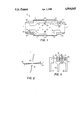
- FIG. 1 is a cross-sectional diagram of the silicon trigger switch semiconductor wafer of the present invention
- FIG. 2 is a voltage-current characteristic curve of the silicon trigger switch of the present invention.
- FIG. 3 is an enlarged top plan view of a device comprising a TRIAC in combination with the silicon trigger switch of the present invention.
- STS 10 is a semiconductor device formed from a wafer of semiconductor material wherein layers of opposite conductivity-type material are formed in both sides of the wafer using conventional masking, diffusion, and etching techniques.
- N-type and P-type semiconductor materials vary. Relative terminology has evolved to distinguish between various doping levels of the same type of semiconductor material in a multilayer device. Normally, a semiconductor material is lightly doped and is termed either N-type or P-type. When a region of heavier doped material is included within the same semiconductor device, it is termed N+ or P+. On the other hand, if there is a region of very lightly doped semiconductor material, it will be termed N- or P-. The "+" or "" symbol denotes relative doping levels, not electrical charge.
- the main body 11 of STS 10 comprises N-type semiconductor material.
- P-type layers 12 and 13 are diffused into both sides of body 11.
- N-type layers 14 and 15 are diffused into portions of P-type layers 12 and 13, respectively.
- the breakover voltage at the junctions between N-type layer 11 and P-type layers 12 and 13 of the basic device is relatively high, approximately 400 volts, depending on the resistivity of the semiconductor slice.
- the breakover voltage can be lowered to approximately 20 volts, for example, by diffusing N+ regions 18 and 19 on the PN junctions between layers 11 and 12 and layers 11 and 13, respectively.
- P+ diffusion regions 20 and 21 can be added to lower the breakover voltage between the P+ and N+ regions to about 8-12 volts.
- P+ layers 16 and 17 may be diffused to prepare the device for ohmic contact.
- the N+ diffusion regions 18 and 19 function to lower the breakover voltage level and allow breakover to occur at the proper PN junction. If breakover occurs at the PN junction on the wrong side of the device, the STS will not switch to the on-state, and high voltage may damage the device.
- isolator grids 24 are etched into each side of the wafer to isolate the PNPN structure from the adjacent inverse PNPN structure.
- the isolator grids 24 work in conjunction with the N+ regions 18 and 19 to ensure that breakover occurs on the proper side of the device and at the proper breakover voltage level.
- the device is completed by adding metallization layers 22 and 23 on both sides of the wafer and adding glass passivation 25 to the exposed junctions of the external grid and the isolator grids 24. Since the isolator grids 24 are etched completely across the top and bottom surfaces of the device, an external connector must span isolator grid 24 and connect both halves of metallization layer 22 to form a first main terminal, and a similar connector must connect both halves of metallization layer 23 to form a second main terminal.
- FIG. 2 shows the bidirectional behavior of STS 10 by illustrating the symmetrical response as STS 10 is biased in the opposite direction. As voltage of opposite polarity increases in magnitude, the device remains in its off-state until breakover point 28 is reached and the device becomes conductive in the opposite direction. Holding current 29 is the minimum current required to maintain the device in its conductive on-state in the opposite direction.
- FIG. 3 illustrates a method of using the silicon trigger switch 10 of the present invention in combination with a TRIAC.
- TRIAC 31 is mounted with its main terminal two (MT2), located on the bottom of the chip, connected directly to MT2 connector 32.
- Main terminal one (MT1) 33 of TRIAC 31 is connected by lead 34 directly to MT1 connector 35.
- the gate 36 of TRIAC 31 is normally connected by lead 37 directly to gate connector 38.
- STS 10 of the present invention may be used in combination as a trigger switch for TRIAC 31. Because STS 10 has its terminals on opposite sides of the chip, STS 10 can be mounted with the bottom terminal connected directly to gate connector 38.
- Contact 39 spans isolator grid 24 of STS 10 and connects both portions of the top terminal 22 of STS 10 to gate 36 of TRIAC 31 via lead 37.
- Leads 34 and 37 may comprise copper bridges, for example.
- the TRIAC/STS device illustrated in FIG. 3 provides an electrical device having the characteristics of a low switching current, a high holding current, and a specific low voltage breakover point of either polarity.
- complicated electronic circuitry comprising a plurality of elements was necessary to provide a low voltage trigger for the TRIAC.
- STS 10 provides a low voltage trigger for TRIAC 31, and the entire circuitry is mounted in a single package having three terminals 32, 35, and 38, which correspond to the three terminals of a TRIAC as used alone in previous applications.
Abstract
Description
Claims (1)
Priority Applications (1)
| Application Number | Priority Date | Filing Date | Title |
|---|---|---|---|
| US07/193,193 US4914045A (en) | 1985-12-19 | 1988-05-09 | Method of fabricating packaged TRIAC and trigger switch |
Applications Claiming Priority (2)
| Application Number | Priority Date | Filing Date | Title |
|---|---|---|---|
| US81116185A | 1985-12-19 | 1985-12-19 | |
| US07/193,193 US4914045A (en) | 1985-12-19 | 1988-05-09 | Method of fabricating packaged TRIAC and trigger switch |
Related Parent Applications (1)
| Application Number | Title | Priority Date | Filing Date |
|---|---|---|---|
| US81116185A Continuation | 1985-12-19 | 1985-12-19 |
Publications (1)
| Publication Number | Publication Date |
|---|---|
| US4914045A true US4914045A (en) | 1990-04-03 |
Family
ID=26888763
Family Applications (1)
| Application Number | Title | Priority Date | Filing Date |
|---|---|---|---|
| US07/193,193 Expired - Fee Related US4914045A (en) | 1985-12-19 | 1988-05-09 | Method of fabricating packaged TRIAC and trigger switch |
Country Status (1)
| Country | Link |
|---|---|
| US (1) | US4914045A (en) |
Cited By (11)
| Publication number | Priority date | Publication date | Assignee | Title |
|---|---|---|---|---|
| US5344794A (en) * | 1993-03-31 | 1994-09-06 | Siemens Components, Inc. | Method of making a semiconductor chip |
| US5516705A (en) * | 1993-09-10 | 1996-05-14 | Teccor Electronics | Method of forming four layer overvoltage protection device |
| US5629215A (en) * | 1996-03-01 | 1997-05-13 | Motorola | Method of fabricating and contacting ultra-small three terminal semiconductor devices |
| US5796123A (en) * | 1995-11-30 | 1998-08-18 | Sgs-Thomson Microelectronics S.A. | Semiconductor component mounted by brazing |
| US6407901B1 (en) | 1999-04-19 | 2002-06-18 | Teccor Electronics, Lp | Semiconductor device providing overvoltage and overcurrent protection for a line |
| US6781161B1 (en) | 2003-04-09 | 2004-08-24 | Teccor Electronics, Lp | Non-gated thyristor device |
| US20040212939A1 (en) * | 2003-04-23 | 2004-10-28 | Casey Kelly C. | Thyristor circuit providing overcurrent protection to a low impedance load |
| US7037814B1 (en) * | 2003-10-10 | 2006-05-02 | National Semiconductor Corporation | Single mask control of doping levels |
| US20060279974A1 (en) * | 2005-06-08 | 2006-12-14 | Gary Hanington | AC line isolated DC high frequency low power converter |
| DE102011076662A1 (en) * | 2011-05-30 | 2012-12-06 | Robert Bosch Gmbh | Semiconductor component and corresponding manufacturing method |
| EP3018710A1 (en) * | 2014-11-10 | 2016-05-11 | Nxp B.V. | Arrangement of semiconductor dies |
Citations (22)
| Publication number | Priority date | Publication date | Assignee | Title |
|---|---|---|---|---|
| US3123750A (en) * | 1961-10-31 | 1964-03-03 | Multiple junction semiconductor device | |
| US3236698A (en) * | 1964-04-08 | 1966-02-22 | Clevite Corp | Semiconductive device and method of making the same |
| US3281628A (en) * | 1964-08-14 | 1966-10-25 | Telefunken Patent | Automated semiconductor device method and structure |
| US3524114A (en) * | 1968-02-29 | 1970-08-11 | Jearld L Hutson | Thyristor having sensitive gate turn-on characteristics |
| US3535615A (en) * | 1967-11-06 | 1970-10-20 | Gen Electric | Power control circuits including a bidirectional current conducting semiconductor |
| US3582762A (en) * | 1968-04-27 | 1971-06-01 | Nippon Denso Co | Integrated circuit semiconductor-type voltage regulator and charging generator apparatus equipped with the same |
| US3609747A (en) * | 1968-12-05 | 1971-09-28 | Bell Telephone Labor Inc | Solid-state display circuit with inherent memory |
| US3835530A (en) * | 1967-06-05 | 1974-09-17 | Texas Instruments Inc | Method of making semiconductor devices |
| US3917962A (en) * | 1973-04-11 | 1975-11-04 | Grigsby Barton Inc | Synchronous switching circuit |
| US3961354A (en) * | 1972-11-17 | 1976-06-01 | Matsushita Electronics Corporation | Mesa type thyristor and its making method |
| US3970843A (en) * | 1973-11-30 | 1976-07-20 | Silec-Semi-Conducteurs | Photosensitive junction devices having controllable sensitivity |
| US4063277A (en) * | 1976-05-28 | 1977-12-13 | Rca Corporation | Semiconductor thyristor devices having breakover protection |
| US4128801A (en) * | 1976-03-11 | 1978-12-05 | Robert Bosch Gmbh | Voltage regulator structure for automotive-type generators |
| US4134778A (en) * | 1977-09-02 | 1979-01-16 | General Electric Company | Selective irradiation of thyristors |
| US4156148A (en) * | 1977-08-18 | 1979-05-22 | Gentron Corporation | Photocoupling structure for a solid state power control device |
| US4224634A (en) * | 1975-06-19 | 1980-09-23 | Asea Aktiebolag | Externally controlled semiconductor devices with integral thyristor and bridging FET components |
| US4242598A (en) * | 1974-10-02 | 1980-12-30 | Varian Associates, Inc. | Temperature compensating transistor bias device |
| US4264917A (en) * | 1978-10-19 | 1981-04-28 | Compagnie Internationale Pour L'informatique Cii-Honeywell Bull | Flat package for integrated circuit devices |
| US4298881A (en) * | 1979-04-06 | 1981-11-03 | Hitachi, Ltd. | Semiconductor device with double moat and double channel stoppers |
| US4320412A (en) * | 1977-06-23 | 1982-03-16 | Western Electric Co., Inc. | Composite material for mounting electronic devices |
| JPS5898914A (en) * | 1981-12-09 | 1983-06-13 | Hitachi Ltd | Manufacture of semiconductor device |
| US4639760A (en) * | 1986-01-21 | 1987-01-27 | Motorola, Inc. | High power RF transistor assembly |
-
1988
- 1988-05-09 US US07/193,193 patent/US4914045A/en not_active Expired - Fee Related
Patent Citations (22)
| Publication number | Priority date | Publication date | Assignee | Title |
|---|---|---|---|---|
| US3123750A (en) * | 1961-10-31 | 1964-03-03 | Multiple junction semiconductor device | |
| US3236698A (en) * | 1964-04-08 | 1966-02-22 | Clevite Corp | Semiconductive device and method of making the same |
| US3281628A (en) * | 1964-08-14 | 1966-10-25 | Telefunken Patent | Automated semiconductor device method and structure |
| US3835530A (en) * | 1967-06-05 | 1974-09-17 | Texas Instruments Inc | Method of making semiconductor devices |
| US3535615A (en) * | 1967-11-06 | 1970-10-20 | Gen Electric | Power control circuits including a bidirectional current conducting semiconductor |
| US3524114A (en) * | 1968-02-29 | 1970-08-11 | Jearld L Hutson | Thyristor having sensitive gate turn-on characteristics |
| US3582762A (en) * | 1968-04-27 | 1971-06-01 | Nippon Denso Co | Integrated circuit semiconductor-type voltage regulator and charging generator apparatus equipped with the same |
| US3609747A (en) * | 1968-12-05 | 1971-09-28 | Bell Telephone Labor Inc | Solid-state display circuit with inherent memory |
| US3961354A (en) * | 1972-11-17 | 1976-06-01 | Matsushita Electronics Corporation | Mesa type thyristor and its making method |
| US3917962A (en) * | 1973-04-11 | 1975-11-04 | Grigsby Barton Inc | Synchronous switching circuit |
| US3970843A (en) * | 1973-11-30 | 1976-07-20 | Silec-Semi-Conducteurs | Photosensitive junction devices having controllable sensitivity |
| US4242598A (en) * | 1974-10-02 | 1980-12-30 | Varian Associates, Inc. | Temperature compensating transistor bias device |
| US4224634A (en) * | 1975-06-19 | 1980-09-23 | Asea Aktiebolag | Externally controlled semiconductor devices with integral thyristor and bridging FET components |
| US4128801A (en) * | 1976-03-11 | 1978-12-05 | Robert Bosch Gmbh | Voltage regulator structure for automotive-type generators |
| US4063277A (en) * | 1976-05-28 | 1977-12-13 | Rca Corporation | Semiconductor thyristor devices having breakover protection |
| US4320412A (en) * | 1977-06-23 | 1982-03-16 | Western Electric Co., Inc. | Composite material for mounting electronic devices |
| US4156148A (en) * | 1977-08-18 | 1979-05-22 | Gentron Corporation | Photocoupling structure for a solid state power control device |
| US4134778A (en) * | 1977-09-02 | 1979-01-16 | General Electric Company | Selective irradiation of thyristors |
| US4264917A (en) * | 1978-10-19 | 1981-04-28 | Compagnie Internationale Pour L'informatique Cii-Honeywell Bull | Flat package for integrated circuit devices |
| US4298881A (en) * | 1979-04-06 | 1981-11-03 | Hitachi, Ltd. | Semiconductor device with double moat and double channel stoppers |
| JPS5898914A (en) * | 1981-12-09 | 1983-06-13 | Hitachi Ltd | Manufacture of semiconductor device |
| US4639760A (en) * | 1986-01-21 | 1987-01-27 | Motorola, Inc. | High power RF transistor assembly |
Non-Patent Citations (3)
| Title |
|---|
| General Electric Co., SCR Manual, p. 110 (6th Ed. 1979). * |
| Teccor Electronics, Inc., General Catalog: Semiconductor Devices, pp. 8 9, 95 103 (1982). * |
| Teccor Electronics, Inc., General Catalog: Semiconductor Devices, pp. 8-9, 95-103 (1982). |
Cited By (14)
| Publication number | Priority date | Publication date | Assignee | Title |
|---|---|---|---|---|
| US5344794A (en) * | 1993-03-31 | 1994-09-06 | Siemens Components, Inc. | Method of making a semiconductor chip |
| US5516705A (en) * | 1993-09-10 | 1996-05-14 | Teccor Electronics | Method of forming four layer overvoltage protection device |
| US5796123A (en) * | 1995-11-30 | 1998-08-18 | Sgs-Thomson Microelectronics S.A. | Semiconductor component mounted by brazing |
| US5629215A (en) * | 1996-03-01 | 1997-05-13 | Motorola | Method of fabricating and contacting ultra-small three terminal semiconductor devices |
| US6407901B1 (en) | 1999-04-19 | 2002-06-18 | Teccor Electronics, Lp | Semiconductor device providing overvoltage and overcurrent protection for a line |
| US6781161B1 (en) | 2003-04-09 | 2004-08-24 | Teccor Electronics, Lp | Non-gated thyristor device |
| US20040212939A1 (en) * | 2003-04-23 | 2004-10-28 | Casey Kelly C. | Thyristor circuit providing overcurrent protection to a low impedance load |
| US6862162B2 (en) | 2003-04-23 | 2005-03-01 | Teccor Electronics, Lp | Thyristor circuit providing overcurrent protection to a low impedance load |
| US7037814B1 (en) * | 2003-10-10 | 2006-05-02 | National Semiconductor Corporation | Single mask control of doping levels |
| US20060279974A1 (en) * | 2005-06-08 | 2006-12-14 | Gary Hanington | AC line isolated DC high frequency low power converter |
| DE102011076662A1 (en) * | 2011-05-30 | 2012-12-06 | Robert Bosch Gmbh | Semiconductor component and corresponding manufacturing method |
| EP3018710A1 (en) * | 2014-11-10 | 2016-05-11 | Nxp B.V. | Arrangement of semiconductor dies |
| US20160133547A1 (en) * | 2014-11-10 | 2016-05-12 | Nxp B.V. | Semiconductor die arrangement |
| US9685396B2 (en) * | 2014-11-10 | 2017-06-20 | Nxp B.V. | Semiconductor die arrangement |
Similar Documents
| Publication | Publication Date | Title |
|---|---|---|
| US3476993A (en) | Five layer and junction bridging terminal switching device | |
| US5430311A (en) | Constant-voltage diode for over-voltage protection | |
| KR900003069B1 (en) | Solid state relay and manufacturing method of this | |
| EP0492558B1 (en) | Semiconductor device comprising a high speed switching bipolar transistor | |
| US5401985A (en) | Low voltage monolithic protection diode with a low capacitance | |
| US4967256A (en) | Overvoltage protector | |
| US3971056A (en) | Semiconductor temperature switches | |
| US4721986A (en) | Bidirectional output semiconductor field effect transistor and method for its maufacture | |
| JPH0669423A (en) | Semiconductor component | |
| KR920010314B1 (en) | Semiconductor device | |
| EP0011443B1 (en) | Semiconductor integrated circuit device | |
| JPS59155964A (en) | Overcurrent protecting device | |
| US4914045A (en) | Method of fabricating packaged TRIAC and trigger switch | |
| US4132996A (en) | Electric field-controlled semiconductor device | |
| US3855611A (en) | Thyristor devices | |
| EP0625797B1 (en) | Integrated structure current sensing resistor for power MOS devices, particularly for overload self-protected power MOS devices | |
| KR920005129B1 (en) | Zener diode emulation and method of forming the same | |
| US3078196A (en) | Semiconductive switch | |
| US3504242A (en) | Switching power transistor with thyristor overload capacity | |
| US5272363A (en) | Bidirectional protection component | |
| US4868703A (en) | Solid state switching device | |
| US4827497A (en) | Electronic trigger switch for maintenance termination unit | |
| US4054893A (en) | Semiconductor switching devices utilizing nonohmic current paths across P-N junctions | |
| EP0084050A4 (en) | Controlled breakover bidirectional semiconductor switch. | |
| US4195306A (en) | Gate turn-off thyristor |
Legal Events
| Date | Code | Title | Description |
|---|---|---|---|
| FPAY | Fee payment |
Year of fee payment: 4 |
|
| REMI | Maintenance fee reminder mailed | ||
| LAPS | Lapse for failure to pay maintenance fees | ||
| FP | Lapsed due to failure to pay maintenance fee |
Effective date: 19980408 |
|
| AS | Assignment |
Owner name: TECCOR DELAWARE, OHIO Free format text: ASSIGNMENT OF ASSIGNORS INTEREST;ASSIGNOR:TECCOR ELECTRONICS, INC.;REEL/FRAME:009453/0173 Effective date: 19980728 Owner name: TECCOR ELECTRONICS, LP, DELAWARE Free format text: ASSIGNMENT OF ASSIGNORS INTEREST;ASSIGNOR:TECCOR DELAWARE INC.;REEL/FRAME:009463/0516 Effective date: 19980729 |
|
| STCH | Information on status: patent discontinuation |
Free format text: PATENT EXPIRED DUE TO NONPAYMENT OF MAINTENANCE FEES UNDER 37 CFR 1.362 |