US4903330A - Housing structure for paging receiver - Google Patents

Housing structure for paging receiver Download PDF

Info

Publication number
US4903330A
US4903330A US07/216,026 US21602688A US4903330A US 4903330 A US4903330 A US 4903330A US 21602688 A US21602688 A US 21602688A US 4903330 A US4903330 A US 4903330A
Authority
US
United States
Prior art keywords
housing
write terminal
window
circuit board
storage device
Prior art date
Legal status (The legal status is an assumption and is not a legal conclusion. Google has not performed a legal analysis and makes no representation as to the accuracy of the status listed.)
Expired - Lifetime
Application number
US07/216,026
Inventor
Tetsumi Ishiguro
Kazumori Yamada
Current Assignee (The listed assignees may be inaccurate. Google has not performed a legal analysis and makes no representation or warranty as to the accuracy of the list.)
NEC Corp
Original Assignee
NEC Corp
Priority date (The priority date is an assumption and is not a legal conclusion. Google has not performed a legal analysis and makes no representation as to the accuracy of the date listed.)
Filing date
Publication date
Application filed by NEC Corp filed Critical NEC Corp
Assigned to NEC CORPORATION reassignment NEC CORPORATION ASSIGNMENT OF ASSIGNORS INTEREST. Assignors: ISHIGURO, TETSUMI, YAMADA, KAZUMORI
Application granted granted Critical
Publication of US4903330A publication Critical patent/US4903330A/en
Anticipated expiration legal-status Critical
Expired - Lifetime legal-status Critical Current

Links

Images

Classifications

    • HELECTRICITY
    • H04ELECTRIC COMMUNICATION TECHNIQUE
    • H04BTRANSMISSION
    • H04B1/00Details of transmission systems, not covered by a single one of groups H04B3/00 - H04B13/00; Details of transmission systems not characterised by the medium used for transmission
    • H04B1/06Receivers
    • H04B1/08Constructional details, e.g. cabinet
    • H04B1/086Portable receivers
    • HELECTRICITY
    • H04ELECTRIC COMMUNICATION TECHNIQUE
    • H04BTRANSMISSION
    • H04B1/00Details of transmission systems, not covered by a single one of groups H04B3/00 - H04B13/00; Details of transmission systems not characterised by the medium used for transmission
    • H04B1/38Transceivers, i.e. devices in which transmitter and receiver form a structural unit and in which at least one part is used for functions of transmitting and receiving
    • H04B1/3816Mechanical arrangements for accommodating identification devices, e.g. cards or chips; with connectors for programming identification devices
    • GPHYSICS
    • G11INFORMATION STORAGE
    • G11CSTATIC STORES
    • G11C16/00Erasable programmable read-only memories
    • G11C16/02Erasable programmable read-only memories electrically programmable
    • G11C16/06Auxiliary circuits, e.g. for writing into memory
    • G11C16/10Programming or data input circuits
    • G11C16/102External programming circuits, e.g. EPROM programmers; In-circuit programming or reprogramming; EPROM emulators
    • G11C16/105Circuits or methods for updating contents of nonvolatile memory, especially with 'security' features to ensure reliable replacement, i.e. preventing that old data is lost before new data is reliably written
    • HELECTRICITY
    • H04ELECTRIC COMMUNICATION TECHNIQUE
    • H04BTRANSMISSION
    • H04B1/00Details of transmission systems, not covered by a single one of groups H04B3/00 - H04B13/00; Details of transmission systems not characterised by the medium used for transmission
    • H04B1/06Receivers
    • H04B1/16Circuits
    • H04B1/1607Supply circuits
    • HELECTRICITY
    • H04ELECTRIC COMMUNICATION TECHNIQUE
    • H04BTRANSMISSION
    • H04B1/00Details of transmission systems, not covered by a single one of groups H04B3/00 - H04B13/00; Details of transmission systems not characterised by the medium used for transmission
    • H04B1/38Transceivers, i.e. devices in which transmitter and receiver form a structural unit and in which at least one part is used for functions of transmitting and receiving
    • H04B2001/3894Waterproofing of transmission device

Landscapes

  • Engineering & Computer Science (AREA)
  • Computer Networks & Wireless Communication (AREA)
  • Signal Processing (AREA)
  • Computer Security & Cryptography (AREA)
  • Mobile Radio Communication Systems (AREA)
  • Casings For Electric Apparatus (AREA)

Abstract

Disclosed is a structure of a housing for a paging receiver of the type including a storage device and a write terminal for a writing code in the storage device. A battery case is disposed in a part of the housing and provided with a window that communicates with the interior of the housing. The write terminal electrically connected to the storage device faces the window so that a connector of a writing apparatus may be inserted into the housing through the window to be connected to the write terminal. The write terminal is not exposed to the outside of the housing, thereby to enhance the resistivity to static electricity and hermetic sealing against dust, water and other impurities and therefore to achieve reliable operation.

Description

BACKGROUND OF THE INVENTION
The present invention relates to the structure of a housing of a paging receiver and, more particularly, to the housing structure of a paging receiver of the type having a storage device and an exclusive write terminal for writing code in the storage device.
There is an increasing demand for a paging receiver which is miniature, inexpensive, reliable and easy to maintain. Particularly as regards structure, the demand for easy maintenance and high reliability is high. A prior art paging receiver usually includes a chamber for accommodating a printed circuit board on which an electrically-erasable programmable read-only-memory (EEPROM) or like storage device for storing a paging number is loaded. Another chamber adjoins the above-mentioned chamber to receive a battery therein. The EEPROM on the printed circuit board is connected by leads to a write terminal for writing the paging number in the EEPROM. The write terminal is provided on the printed circuit board or mounted on an exterior part of a housing of the receiver to show itself for easy access from the outside.
A drawback with the arrangement wherein the write terminal is mounted on the printed circuit board is that the code cannot be written in the EEPROM without disassembling the housing in which the printed circuit board is accommodated and then connecting a writing apparatus to the write terminal. This not only entails troublesome operation but also runs contrary to the demand for easy maintenance. On the other hand, the write terminal fitted to a part of the housing creates the problem that static electricity is apt to be conducted to the EEPROM and various integrated circuits via the write terminal. Such static electricity would destroy the code stored in the EEPROM, cause the receiver to malfunction, and even destroy the whole circuitry in the receiver, critically lowering the reliability of the receiver.
SUMMARY OF THE INVENTION
It is therefore an object of the present invention to provide a housing structure for a paging receiver that facilitates maintenance, promotes easy writing of code, and has a high reliability of operation.
It is another object of the present invention to provide a generally improved housing structure for a paging receiver.
A housing structure for a paging receiver of the present invention comprises a chamber for accommodating a printed circuit board on which at least a storage device for storing code and a write terminal for writing the code in the storage device are mounted; a battery case provided in a space which adjoins the chamber and having an opening which is exposed to the outside; and a window formed through a part of the battery case that adjoins the chamber and communicates with the chamber. The write terminal is located on the printed circuit board in such a manner as to face the window, such that the write terminal is connectible to a connector of a writing apparatus that is inserted through the window as needed.
BRIEF DESCRIPTION OF THE DRAWINGS
The above and other objects, features and advantages of the present invention will become more apparent from the following detailed description taken with the accompanying drawings, in which:
FIGS. 1 and 2 are perspective views each showing a different prior art housing structure for a paging receiver;
FIG. 3 is a perspective view showing a housing structure embodying the present invention;
FIG. 4 is a fragmentary section along line IV--IV of FIG. 3;
FIG. 5 is a perspective view demonstrating how to write a paging number with the embodiment of FIG. 3;
FIG. 6 is a fragmentary section associated with FIG. 5;
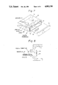
FIG. 7 is a perspective view showing another embodiment of the present invention; and
FIG. 8 is a fragmentary section associated with FIG. 7.
DESCRIPTION OF THE PREFERRED EMBODIMENTS
To better understand the present invention, a brief reference will be made to prior art housing structures for a paging receiver which are shown in FIGS. 1 and 2.
Referring to FIG. 1, a prior art housing 10 for a paging receiver accommodates therein an EEPROM or similar storage device 12 for storing desired code which is assigned to the paging receiver. A battery case 14 for receiving a battery therein is built in the housing 10 so that a chamber 16 is defined by the battery case 14 and the housing 10. A printed circuit board (PCB) 18 is disposed in the chamber 16. The battery case 14 has an opening 20 which is usually closed by a lid 22 which forms a part of the housing 10. The EEPROM 12 is mounted on the printed circuit board 18 and connected by leads 26 and 28 to a write terminal 24 so that the code may be written in the EEPROM 12 via the terminal 24. While the write terminal 24 shown in FIG. 1 is directly mounted on the printed circuit board 18, it may be mounted in a part 10a of the housing 10 as shown in FIG. 2.
Each of the prior art housing structures shown and described has a problem left unsolved, as previously stated. Specifically, with the arrangement of FIG. 1, it is necessary to write code in the EEPROM 12 by disassembling the housing 10 in which the printed circuit board 18 is accommodated and then connecting a writing apparatus (not shown) to the write terminal 24. This is not only troublesome but also objectionable from the easy maintenance standpoint. On the other hand, the structure of FIG. 2 suffers from a drawback that static electricity is apt to be conducted to the EEPROM 12 and various integrated circuits via the write terminal 24 which is exposed to the outside through the housing 10a. Such static electricity would destroy the data stored in the EEPROM 12, cause the receiver to malfunction, and even destroy the whole circuitry stored in the receiver, critically lowering the reliability of the receiver.
Referring to FIGS. 3 to 8, there are shown preferred embodiments of the present invention which are free from the drawbacks particular to the prior art housing structures as discussed above. In FIGS. 3 to 8, the same or similar structural elements as those shown in FIGS. 1 and 2 are designated by like reference numerals.
In FIGS. 3 and 4, a housing 10 in accordance with the present invention is generally configured in a rectangular parallelepiped. A battery case 14 is built in the housing 10 adjacent to an opening 20 of the housing 10 and defines a chamber 16 in cooperation with the housing 10. A lid 22 is removably mounted on the housing 10 to close the opening 20 while forming a part of the housing 10, whereby a chamber for receiving a battery (not shown) is defined. The housing 10, battery case 14 and lid 22 are each made of a non-conductive material such as polycarbonate. A printed circuit board 18 is disposed in the chamber 16 while an EEPROM 12 is mounted on the circuit board 18 together with various kinds of circuit parts. A write terminal 24 is loaded in one end portion of the printed circuit board 18 and electrically connected to the EEPROM 12 by leads 26 and 28. That part of the battery case 14 which faces the write terminal 24 is provided with an opening or window 14a. This window 14a allows a connector 32 of a writing apparatus 30 which will be now described with reference to FIGS. 5 and 6 to be inserted through the window 14a into electrical connection with the write terminal 24.
FIGS. 5 and 6 show how a desired code is written in the EEPROM 12. Specifically, the lid 22 (FIG. 3) is removed to expose the battery case 14 to the outside, and then the connector 32 connected to the writing apparatus 30 by wiring 34 is inserted into the housing 10 via the window 14a to be connected to the write terminal 24. In this condition, a code may be written in the EEPROM 12 which is connected to the writing apparatus 30 via the write terminal 24 and leads 26 and 28. In FIG. 6, the reference numeral 36 designated a resilient contact for connection.
In this particular embodiment, although the write terminal 24 is entirely accommodated in the housing 10, a code can be written in the EEPROM 12 merely by removing the lid 22 and inserting the connector 32 through the window 14a of the battery case 14 into connection with the write terminal 24. This facilitates writing operation and promotes easy maintenance.
As shown in FIG. 4, assume that the distance between the write terminal 24 and the inner surface of the battery case 14 is a, the thickness of the battery case 14 is b, the inside dimension of the battery case 14 is c, and the thickness of the lid 22 is d. Then, the write terminal 24 which is not exposed to the outside is spaced apart from the outer surface of the battery case 14 by a distance a+b and, when the lid 22 is attached to the housing 10, it is spaced apart from the outer surface of the lid 22 by a distance a+b+c+d. The influence of static electricity developed outside the housing 10 on the interior of the housing 10 is reduced in proportion to the distance a+b or a+b+c+d to protect the EEPROM 12 and other various circuit parts from destruction. Such a structure, therefore, enhances reliable operations of the paging receiver.
Referring to FIGS. 7 and 8, another embodiment of the present invention is shown. This embodiment is essentially similar to the previous embodiment except that a non-conductive label 38 is adhered to the battery case 14 to close the window 14a, the label 38 showing the code which is stored in the EEPROM 12. This alternative embodiment has an advantage that a person can see the label 38 and therefore the content stored in the EEPROM 12 simply by removing the lid 22, not to speak of the various advantages described in relation to the first embodiment. In addition, the label 38 which closes the window 14a further enhances the resistivity of the EEPROM 12 and others to static electricity and prevents dust, water and other impurities from reaching the write terminal 24 and printed circuit board 18 through the window 14a.
In summary, a housing for a paging receiver in accordance with the present invention includes a battery case that forms a part of the housing and communicates with the interior of the housing through a window. A connector of a writing apparatus may be inserted into the housing through the window into connection with a write terminal that is electrically connected to a storage device. Hence, a code can be written in the storage device simply by removing a lid that is adapted to close the battery case. This promotes easy writing operation as well as easy maintenance. Since the write terminal is not exposed to the outside of the housing, resistivity to static electricity and hermetic sealing against impurities are enhanced to offer unprecedented reliability of operation.
Although the present invention has been described in relation to particular embodiments thereof, many other variations and modifications and other uses will become apparent to those skilled in the art. It is preferred, therefore, that the present invention be limited not by the specific disclosure herein, but only by the appended claims.

Claims (7)

What is claimed is:
1. A housing structure for a paging receiver comprising:
a printed-circuit board on which are mounted at least a storage device for storing code and a write terminal for writing the code in the storage device;
a chamber for accommodating said printed-circuit board;
a battery chamber that is spaced from the printedcircuit board chamber by an internal separating wall and that has an opening to permit battery insertion and removal from the outside;
said internal separating wall having a window with an opening in said printed-circuit board chamber in proximity to the portion of said printed-circuit board on which said write terminal is mounted, and with a further opening in said battery chamber for allowing a connector of a writing apparatus to be inserted through the window and into contact with said write terminal.
2. A structure as claimed in claim 1, further comprising a label that closes said window.
3. A structure as claimed in claim 2, wherein said label is adhesive and non-conductive.
4. A structure as claimed in claim 2, wherein said label shows the code that is stored in said storage device.
5. A structure as claimed in claim 1, further comprising a lid for closing said opening of said battery case.
6. A structure as claimed in claim 5, wherein said housing, said battery case and said lid each comprises non-conductive material.
7. A structure as claimed in claim 1, wherein said window is positioned and shaped to receive a portion of said printed-circuit board on which said write terminal is mounted.
US07/216,026 1987-07-07 1988-07-07 Housing structure for paging receiver Expired - Lifetime US4903330A (en)

Applications Claiming Priority (2)

Application Number Priority Date Filing Date Title
JP62167756A JPH0797506B2 (en) 1987-07-07 1987-07-07 Selective call receiver housing structure
JP62-167756 1987-07-07

Publications (1)

Publication Number Publication Date
US4903330A true US4903330A (en) 1990-02-20

Family

ID=15855510

Family Applications (1)

Application Number Title Priority Date Filing Date
US07/216,026 Expired - Lifetime US4903330A (en) 1987-07-07 1988-07-07 Housing structure for paging receiver

Country Status (8)

Country Link
US (1) US4903330A (en)
EP (1) EP0298720B1 (en)
JP (1) JPH0797506B2 (en)
KR (1) KR910004401B1 (en)
AU (1) AU603750B2 (en)
CA (1) CA1290023C (en)
DE (1) DE3851798T2 (en)
HK (1) HK84397A (en)

Cited By (5)

* Cited by examiner, † Cited by third party
Publication number Priority date Publication date Assignee Title
US5155860A (en) * 1988-12-27 1992-10-13 Cellular Communications Corporation Cellular portable telephone battery pack and programmer interface
US5230092A (en) * 1989-07-21 1993-07-20 Seiko Epson Corporation Read/write device and apparatus and method for reading from and writing into the device
US5320561A (en) * 1992-06-19 1994-06-14 Motorola, Inc. Connector for providing programming, testing, and power signals
GB2293506A (en) * 1994-09-22 1996-03-27 Nec Corp Pager receiver with locking means for battery cover which hides input terminal
US6195532B1 (en) 1996-06-28 2001-02-27 At&T Wireless Srcs. Inc. Method for categorization of multiple providers in a wireless communications service environment

Families Citing this family (2)

* Cited by examiner, † Cited by third party
Publication number Priority date Publication date Assignee Title
JPH0739267Y2 (en) * 1987-07-10 1995-09-06 日本電気株式会社 Portable holder housing
US20030095656A1 (en) * 2001-11-20 2003-05-22 Sommer Henry David Rugged design and method for housing an electronic device

Citations (9)

* Cited by examiner, † Cited by third party
Publication number Priority date Publication date Assignee Title
US4417246A (en) * 1979-11-19 1983-11-22 General Electric Company Paging receiver having a serial code plug
US4558270A (en) * 1983-09-06 1985-12-10 James P. Liautaud Battery charging adapter for a battery charger for a portable battery operated transceiver
US4593409A (en) * 1984-04-04 1986-06-03 Motorola, Inc. Transceiver protection arrangement
US4639726A (en) * 1983-08-18 1987-01-27 Nec Corporation Radio communication apparatus disabled on reception of a predetermined signal
US4688262A (en) * 1986-03-26 1987-08-18 General Electric Company Externally connectable control unit for a portable radio
US4709201A (en) * 1985-10-24 1987-11-24 General Electric Company Portable radio battery pack with on-off switch
US4761823A (en) * 1986-09-05 1988-08-02 E. F. Johnson Company Communications adaptor bracket
US4771399A (en) * 1985-12-31 1988-09-13 Motorola, Inc. Method and apparatus for programming memory through battery terminals
US4786889A (en) * 1985-12-10 1988-11-22 Nec Corporation Battery casing for a paging receiver

Family Cites Families (5)

* Cited by examiner, † Cited by third party
Publication number Priority date Publication date Assignee Title
JPS603635Y2 (en) * 1978-12-07 1985-02-01 株式会社東芝 Control power connection device for differential relay case
JPS56105213U (en) * 1980-01-16 1981-08-17
NL176889C (en) * 1980-01-30 1985-06-17 Nira Int Bv PERSON SEARCH RECEIVER.
JPH0244108B2 (en) * 1984-07-25 1990-10-02 Matsushita Electric Works Ltd DENWA JATSUKU
JPS6167295A (en) * 1984-09-10 1986-04-07 日本電気株式会社 Housing structure of radio wave device

Patent Citations (9)

* Cited by examiner, † Cited by third party
Publication number Priority date Publication date Assignee Title
US4417246A (en) * 1979-11-19 1983-11-22 General Electric Company Paging receiver having a serial code plug
US4639726A (en) * 1983-08-18 1987-01-27 Nec Corporation Radio communication apparatus disabled on reception of a predetermined signal
US4558270A (en) * 1983-09-06 1985-12-10 James P. Liautaud Battery charging adapter for a battery charger for a portable battery operated transceiver
US4593409A (en) * 1984-04-04 1986-06-03 Motorola, Inc. Transceiver protection arrangement
US4709201A (en) * 1985-10-24 1987-11-24 General Electric Company Portable radio battery pack with on-off switch
US4786889A (en) * 1985-12-10 1988-11-22 Nec Corporation Battery casing for a paging receiver
US4771399A (en) * 1985-12-31 1988-09-13 Motorola, Inc. Method and apparatus for programming memory through battery terminals
US4688262A (en) * 1986-03-26 1987-08-18 General Electric Company Externally connectable control unit for a portable radio
US4761823A (en) * 1986-09-05 1988-08-02 E. F. Johnson Company Communications adaptor bracket

Non-Patent Citations (2)

* Cited by examiner, † Cited by third party
Title
"Electronic Engineers Masters Catalog", Hearst, 1982, p. 2100.
Electronic Engineers Masters Catalog , Hearst, 1982, p. 2100. *

Cited By (7)

* Cited by examiner, † Cited by third party
Publication number Priority date Publication date Assignee Title
US5155860A (en) * 1988-12-27 1992-10-13 Cellular Communications Corporation Cellular portable telephone battery pack and programmer interface
US5230092A (en) * 1989-07-21 1993-07-20 Seiko Epson Corporation Read/write device and apparatus and method for reading from and writing into the device
US5678203A (en) * 1989-07-21 1997-10-14 Seiko Epson Corporation Read/write terminal construction for an information receiving and transmitting device
US5320561A (en) * 1992-06-19 1994-06-14 Motorola, Inc. Connector for providing programming, testing, and power signals
GB2293506A (en) * 1994-09-22 1996-03-27 Nec Corp Pager receiver with locking means for battery cover which hides input terminal
GB2293506B (en) * 1994-09-22 1999-03-10 Nec Corp Housing for pager receiver
US6195532B1 (en) 1996-06-28 2001-02-27 At&T Wireless Srcs. Inc. Method for categorization of multiple providers in a wireless communications service environment

Also Published As

Publication number Publication date
DE3851798T2 (en) 1995-05-18
JPS6412474A (en) 1989-01-17
EP0298720A3 (en) 1990-12-19
CA1290023C (en) 1991-10-01
KR910004401B1 (en) 1991-06-27
JPH0797506B2 (en) 1995-10-18
KR890003152A (en) 1989-04-13
HK84397A (en) 1997-06-27
AU603750B2 (en) 1990-11-22
AU1870688A (en) 1989-01-12
EP0298720B1 (en) 1994-10-12
DE3851798D1 (en) 1994-11-17
EP0298720A2 (en) 1989-01-11

Similar Documents

Publication Publication Date Title
JP3167244B2 (en) Shielded memory card holder
SE8702904L (en) Memory Cassette
US7484981B2 (en) Assembly for sealing an audio connector within an electronic device
US4903330A (en) Housing structure for paging receiver
KR100238909B1 (en) Ic card reading/writing device
CN101499139B (en) Electronic card
US4919624A (en) Connection terminal structure of electronic equipment
JP2829796B2 (en) Electronic equipment housing
US5240792A (en) Battery holder for electronic apparatus
US4812950A (en) Means for mounting a ROM on a printed circuit board
JPH1117792A (en) Radio type individual receiver
JP2006331267A (en) Electronic apparatus having communication terminal
JP2006172478A (en) Thin usb electronic device
JPH0832493B2 (en) Portable storage device and its connection mechanism
US6513722B1 (en) Cartridge and memory medium comprising cartridge and plate memory
JPH07288117A (en) Battery case structure and protecting cover
US6485117B1 (en) Data card drawer and method of use
JPS603878A (en) Connector for hybrid integrated circuit unit
JPH0684022A (en) Electronic apparatus
KR0118175Y1 (en) Battery mounting structure
JPH0621834A (en) Selective calling receiver
JP3307738B2 (en) Electronic device housing structure
US20030147223A1 (en) Memory adapter module for portable computer
KR820001108B1 (en) Interchangeable module for integrated circuits
JPH0619259U (en) Battery case structure and protective cover

Legal Events

Date Code Title Description
AS Assignment

Owner name: NEC CORPORATION 33-1, SHIBA 5-CHOME, MINATO-KU, TO

Free format text: ASSIGNMENT OF ASSIGNORS INTEREST.;ASSIGNORS:ISHIGURO, TETSUMI;YAMADA, KAZUMORI;REEL/FRAME:004907/0195

Effective date: 19880627

Owner name: NEC CORPORATION,JAPAN

Free format text: ASSIGNMENT OF ASSIGNORS INTEREST;ASSIGNORS:ISHIGURO, TETSUMI;YAMADA, KAZUMORI;REEL/FRAME:004907/0195

Effective date: 19880627

STCF Information on status: patent grant

Free format text: PATENTED CASE

FEPP Fee payment procedure

Free format text: PAYOR NUMBER ASSIGNED (ORIGINAL EVENT CODE: ASPN); ENTITY STATUS OF PATENT OWNER: LARGE ENTITY

FPAY Fee payment

Year of fee payment: 4

FPAY Fee payment

Year of fee payment: 8

FEPP Fee payment procedure

Free format text: PAYER NUMBER DE-ASSIGNED (ORIGINAL EVENT CODE: RMPN); ENTITY STATUS OF PATENT OWNER: LARGE ENTITY

FEPP Fee payment procedure

Free format text: PAYOR NUMBER ASSIGNED (ORIGINAL EVENT CODE: ASPN); ENTITY STATUS OF PATENT OWNER: LARGE ENTITY

FPAY Fee payment

Year of fee payment: 12