US4742378A - Junction-type semiconductor light emitting device with mesa - Google Patents
Junction-type semiconductor light emitting device with mesa Download PDFInfo
- Publication number
- US4742378A US4742378A US06/784,890 US78489085A US4742378A US 4742378 A US4742378 A US 4742378A US 78489085 A US78489085 A US 78489085A US 4742378 A US4742378 A US 4742378A
- Authority
- US
- United States
- Prior art keywords
- plate portion
- column
- junction
- semiconductor
- refractive index
- Prior art date
- Legal status (The legal status is an assumption and is not a legal conclusion. Google has not performed a legal analysis and makes no representation as to the accuracy of the status listed.)
- Expired - Lifetime
Links
Images


Classifications
-
- H—ELECTRICITY
- H01—ELECTRIC ELEMENTS
- H01L—SEMICONDUCTOR DEVICES NOT COVERED BY CLASS H10
- H01L33/00—Semiconductor devices with at least one potential-jump barrier or surface barrier specially adapted for light emission; Processes or apparatus specially adapted for the manufacture or treatment thereof or of parts thereof; Details thereof
- H01L33/02—Semiconductor devices with at least one potential-jump barrier or surface barrier specially adapted for light emission; Processes or apparatus specially adapted for the manufacture or treatment thereof or of parts thereof; Details thereof characterised by the semiconductor bodies
- H01L33/20—Semiconductor devices with at least one potential-jump barrier or surface barrier specially adapted for light emission; Processes or apparatus specially adapted for the manufacture or treatment thereof or of parts thereof; Details thereof characterised by the semiconductor bodies with a particular shape, e.g. curved or truncated substrate
- H01L33/24—Semiconductor devices with at least one potential-jump barrier or surface barrier specially adapted for light emission; Processes or apparatus specially adapted for the manufacture or treatment thereof or of parts thereof; Details thereof characterised by the semiconductor bodies with a particular shape, e.g. curved or truncated substrate of the light emitting region, e.g. non-planar junction
-
- B—PERFORMING OPERATIONS; TRANSPORTING
- B82—NANOTECHNOLOGY
- B82Y—SPECIFIC USES OR APPLICATIONS OF NANOSTRUCTURES; MEASUREMENT OR ANALYSIS OF NANOSTRUCTURES; MANUFACTURE OR TREATMENT OF NANOSTRUCTURES
- B82Y20/00—Nanooptics, e.g. quantum optics or photonic crystals
-
- H—ELECTRICITY
- H01—ELECTRIC ELEMENTS
- H01S—DEVICES USING THE PROCESS OF LIGHT AMPLIFICATION BY STIMULATED EMISSION OF RADIATION [LASER] TO AMPLIFY OR GENERATE LIGHT; DEVICES USING STIMULATED EMISSION OF ELECTROMAGNETIC RADIATION IN WAVE RANGES OTHER THAN OPTICAL
- H01S5/00—Semiconductor lasers
- H01S5/06—Arrangements for controlling the laser output parameters, e.g. by operating on the active medium
- H01S5/062—Arrangements for controlling the laser output parameters, e.g. by operating on the active medium by varying the potential of the electrodes
- H01S5/06209—Arrangements for controlling the laser output parameters, e.g. by operating on the active medium by varying the potential of the electrodes in single-section lasers
-
- H—ELECTRICITY
- H01—ELECTRIC ELEMENTS
- H01S—DEVICES USING THE PROCESS OF LIGHT AMPLIFICATION BY STIMULATED EMISSION OF RADIATION [LASER] TO AMPLIFY OR GENERATE LIGHT; DEVICES USING STIMULATED EMISSION OF ELECTROMAGNETIC RADIATION IN WAVE RANGES OTHER THAN OPTICAL
- H01S5/00—Semiconductor lasers
- H01S5/10—Construction or shape of the optical resonator, e.g. extended or external cavity, coupled cavities, bent-guide, varying width, thickness or composition of the active region
- H01S5/18—Surface-emitting [SE] lasers, e.g. having both horizontal and vertical cavities
- H01S5/183—Surface-emitting [SE] lasers, e.g. having both horizontal and vertical cavities having only vertical cavities, e.g. vertical cavity surface-emitting lasers [VCSEL]
- H01S5/18344—Surface-emitting [SE] lasers, e.g. having both horizontal and vertical cavities having only vertical cavities, e.g. vertical cavity surface-emitting lasers [VCSEL] characterized by the mesa, e.g. dimensions or shape of the mesa
- H01S5/18347—Mesa comprising active layer
-
- H—ELECTRICITY
- H01—ELECTRIC ELEMENTS
- H01S—DEVICES USING THE PROCESS OF LIGHT AMPLIFICATION BY STIMULATED EMISSION OF RADIATION [LASER] TO AMPLIFY OR GENERATE LIGHT; DEVICES USING STIMULATED EMISSION OF ELECTROMAGNETIC RADIATION IN WAVE RANGES OTHER THAN OPTICAL
- H01S5/00—Semiconductor lasers
- H01S5/10—Construction or shape of the optical resonator, e.g. extended or external cavity, coupled cavities, bent-guide, varying width, thickness or composition of the active region
- H01S5/18—Surface-emitting [SE] lasers, e.g. having both horizontal and vertical cavities
- H01S5/185—Surface-emitting [SE] lasers, e.g. having both horizontal and vertical cavities having only horizontal cavities, e.g. horizontal cavity surface-emitting lasers [HCSEL]
-
- H—ELECTRICITY
- H01—ELECTRIC ELEMENTS
- H01S—DEVICES USING THE PROCESS OF LIGHT AMPLIFICATION BY STIMULATED EMISSION OF RADIATION [LASER] TO AMPLIFY OR GENERATE LIGHT; DEVICES USING STIMULATED EMISSION OF ELECTROMAGNETIC RADIATION IN WAVE RANGES OTHER THAN OPTICAL
- H01S5/00—Semiconductor lasers
- H01S5/02—Structural details or components not essential to laser action
- H01S5/026—Monolithically integrated components, e.g. waveguides, monitoring photo-detectors, drivers
- H01S5/0262—Photo-diodes, e.g. transceiver devices, bidirectional devices
- H01S5/0264—Photo-diodes, e.g. transceiver devices, bidirectional devices for monitoring the laser-output
-
- H—ELECTRICITY
- H01—ELECTRIC ELEMENTS
- H01S—DEVICES USING THE PROCESS OF LIGHT AMPLIFICATION BY STIMULATED EMISSION OF RADIATION [LASER] TO AMPLIFY OR GENERATE LIGHT; DEVICES USING STIMULATED EMISSION OF ELECTROMAGNETIC RADIATION IN WAVE RANGES OTHER THAN OPTICAL
- H01S5/00—Semiconductor lasers
- H01S5/06—Arrangements for controlling the laser output parameters, e.g. by operating on the active medium
- H01S5/062—Arrangements for controlling the laser output parameters, e.g. by operating on the active medium by varying the potential of the electrodes
- H01S5/06233—Controlling other output parameters than intensity or frequency
- H01S5/06243—Controlling other output parameters than intensity or frequency controlling the position or direction of the emitted beam
-
- H—ELECTRICITY
- H01—ELECTRIC ELEMENTS
- H01S—DEVICES USING THE PROCESS OF LIGHT AMPLIFICATION BY STIMULATED EMISSION OF RADIATION [LASER] TO AMPLIFY OR GENERATE LIGHT; DEVICES USING STIMULATED EMISSION OF ELECTROMAGNETIC RADIATION IN WAVE RANGES OTHER THAN OPTICAL
- H01S5/00—Semiconductor lasers
- H01S5/20—Structure or shape of the semiconductor body to guide the optical wave ; Confining structures perpendicular to the optical axis, e.g. index or gain guiding, stripe geometry, broad area lasers, gain tailoring, transverse or lateral reflectors, special cladding structures, MQW barrier reflection layers
- H01S5/2004—Confining in the direction perpendicular to the layer structure
- H01S5/2018—Optical confinement, e.g. absorbing-, reflecting- or waveguide-layers
- H01S5/2027—Reflecting region or layer, parallel to the active layer, e.g. to modify propagation of the mode in the laser or to influence transverse modes
-
- H—ELECTRICITY
- H01—ELECTRIC ELEMENTS
- H01S—DEVICES USING THE PROCESS OF LIGHT AMPLIFICATION BY STIMULATED EMISSION OF RADIATION [LASER] TO AMPLIFY OR GENERATE LIGHT; DEVICES USING STIMULATED EMISSION OF ELECTROMAGNETIC RADIATION IN WAVE RANGES OTHER THAN OPTICAL
- H01S5/00—Semiconductor lasers
- H01S5/30—Structure or shape of the active region; Materials used for the active region
- H01S5/34—Structure or shape of the active region; Materials used for the active region comprising quantum well or superlattice structures, e.g. single quantum well [SQW] lasers, multiple quantum well [MQW] lasers or graded index separate confinement heterostructure [GRINSCH] lasers
- H01S5/3428—Structure or shape of the active region; Materials used for the active region comprising quantum well or superlattice structures, e.g. single quantum well [SQW] lasers, multiple quantum well [MQW] lasers or graded index separate confinement heterostructure [GRINSCH] lasers layer orientation perpendicular to the substrate
Definitions
- the present invention relates to semiconductor light emitting devices which are usable as light emitting diodes and laser diodes, and more particularly to a junction-type semiconductor light emitting device whose pn junction is formed perpendicular to a substrate or like plate portion to provide an active region for emitting light in the vertical direction.
- Light emitting devices which radiate light perpendicular to the substrate can be easily coupled to optical fibers and are expected to find various uses as surface emitting light sources. Efforts have therefore been made to develop these devices in the field of research on laser diodes and light emitting diodes, and a wide variety of such devices are in use in recent years.
- the pn junction is positioned in parallel with the substrate to provide an active region which is usually as small as 2 to 3 ⁇ m in thickness. Consequently, a gain which is needed for causing the device of this type to produce laser oscillation of sufficient intensity perpendicular to the substrate.
- the device substantially has the fatal drawback that it is difficult to realize continuous oscillation at room temperature as essentially required of useful laser diodes.
- the so-called “facial light emitting” device constructed such as the resultant light is emitted in the direction of thickness perpendicular to the device substrate is widely used in the from of light emitting diode.
- the light emitting device of this kind has been developed as regarded as a light emitting diode having a wide light emitting surface, meanwhile the possibility of realization of a facial light emitting device provided with the function of semiconductor laser.
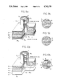
- the conventional facial light emitting device of this kind particularly, the conventional facial light emitting semiconductor laser device is constructed as shown in FIG. 1, that is, as operated as a laser device by basically forming an optical resonator in a manner such as clad layers and a reflector layer are provided on an upper and a lower surfaces of an active region of a facial light emitting type light emitting diode, the latter being sandwiched by the formers.
- an intermediate layer 1 having thickness d is sandwiched by clad layers 2 and 3 consisting of a material having a wide energy gap, so as to form a sandwich structure.
- the thicker clad layer 2 as shown in FIG. 1 is formed as of n-type, meanwhile the other clad layer 3 is formed as of p-type.
- an annular electrode 8 and a circular electrode 6 are provided, respectively, as shown in FIG.
- the circular electrode 6 provided on the lower surface of the sandwich structure is operated as a reflective mirror, as well as a translucent mirror 7 is provided in a central blank of the annular electrode 8 provided on the upper surface of the sandwich structure, so as to form the optical resonator PR.
- the laser oscillation is effected, the output laser light PO resulted therefrom being taken out through the translucent mirror 7.
- the conventional facial light emitting device of this kind for instance, in the conventional facial light emitting semiconductor laser device, the pn junction, through which the carriers are injected, is formed in the vertical direction, that is, in the direction of thickness of the sandwich structure and hence the thickness of the active region is restricted by the diffusion length of the carriers.
- an extremely large injection current density is necessitated. So that, the conventional facial light emitting semiconductor laser device essentially has such a fatal defect over the merit of facial light emission that it is difficult to realize the continuous oscilation at room temperature as an unavoidable condition of the semiconductor laser device for practical use.
- An object of the present invention is to provide a junction-type semiconductor light emitting device which has a pn junction perpendicular to a plate portion such as a substrate and which is adapted for perpendicular radiation.
- Another object of the present invention is to provide a junction-type semiconductor light emitting device which can be fabricated easily by the planar process and which has a large gain effectively perpendicular to its substrate or plate portion.
- Another object of the invention is to provide a junction-type semiconductor light emitting device which can be fabricated by facilitated two-dimensional integration and is therefore adapted to have the desired emission pattern for use as a surface emitting light source.
- Another object of the invention is to provide a junction-type semiconductor light emitting device which can be coupled to communication optical fibers easily with high efficiency.
- Another object of the invention is to provide a junction-type semiconductor light emitting device which includes optical resonating means comprising amplifying means and a reflecting element for optical feedback, and is usable as a laser diode with a low threshold current value required for continuous oscillation at room temperature.
- Still another object of the invention is to provide a junction-type semiconductor light emitting device which is useful as a laser diode, light emitting diode, optical amplifier, optical logic device, optical memory element, optical computer, optical audio disk, optical video disk, POS, light-pen or the like and which is suitable as a component of systems for optical measurement, optical communication, optical information processing, etc.
- the present invention provides a junction type semiconductor light emitting device comprising a plate portion, a column formed on one surface of the plate portion and electrodes provided on each of opposite surfaces of the plate portion, the column having a tubular pn junction formed therein and extending perpendicular to the plate portion, the plate portion having a pn junction formed therein and extending in parallel with the plate portion, the current density of a circuit through the pn junction in the column being greater than 0.1 times the current density of a circuit through the pn junction in the plate portion, when a predetermined voltage is applied across the electrodes.
- FIG. 1 is a sectional view of an example of the conventional light emitting device as described earlier;
- FIGS. 2(a), (b) and (c) are sectional views of light emitting devices for illustrating the basic feature of the present invention
- FIGS. 3-4, 5A-5B, 6A-6B, 7A-7B, 8A-8B, 9A-9C, 10A-10B and 11 are perspective views partly in section and showing different embodiments of the invention.
- FIG. 12 is a sectional view showing another embodiment of the invention.
- FIG. 13 is a perspective view showing still another embodiment of the invention.
- the light emitting device of the present invention comprises a plate portion B, a column P formed on one surface of the plate portion B, an electrode E1 provided on the peripheral side surface of the column P and on the upper surface of the plate portion B, and an electrode E2 provided on the lower surface of the plate portion B.
- the column P has a tubular pn junction PN1 formed therein and extending perpendicular to the plate portion B.
- the plate portion B has a pn junction PN2 formed therein and extending in parallel with the plate portion B.
- the pn junction PN1 may be continuous with the pn junction PN2 as shown in FIG. 2(a), or they may be separate junctions.
- the pn junction PN1 In order to produce an emission perpendicular to the plate portion B, the pn junction PN1 only of the two junctions is of use, and the presence of the pn junction PN2 is essentially objectionable. Nevertheless, the presence of the pn junction, if allowed, eliminates all the preparations and ingenuities that would otherwise be needed for the fabrication of the present device so as not to form the pn junction, consequently assuring commercial quantity production of the device at a reduced cost. According to the present invention, however, it is essential to fulfill the following requirement as to a current density difference in order to realize useful perpendicular emission in the presence of the pn junction PN2.
- the present device has the relation of
- the current density J1 is preferably less than 100 kA/cm 2 , more preferably less than 20 kA/cm 2 , most preferably less than 10 kA/cm 2
- the current density J2 is preferably less than 10 kA/cm 2 , more preferably less than 1 kA/cm 2 .
- the plate portion is cut one only locally immediately below the column P to reduce the electric resistance of the circuit C1.
- the electrodes E1 and E2 need not always be provided over the entire area of the front surface and rear surface, respectively, of the plate portion B but may be formed only at the required locations. The foregoing relation of the current densities can therefore be realized also by giving consideration to the shape or position of the electrodes E1 and E2.
- the above relation can be established by providing the electrode E2 over the entire rear surface of the plate portion B and forming the electrode E1 only on the peripheral side surface of the column P or, conversely, by providing the electrode E1 over the peripheral side surface of the column P and over the entire front surface of the plate portion B as shown in FIG. 2(a) and forming the electrode E2 on the rear surface of the plate portion B only locally immediately below the column P or in the vicinity of this location.
- the current densities J1, J2 can be measured, for example, by the following method.
- an annular incision is formed in the plate portion B around the column P by reactive ion etching or other suitable method, to a depth sufficient to disconnect the pn junction PN1 from the pn junction PN2 to separate the circuits C1 and C2 from each other.
- the incision divides the electrode E1 into one electrode portion E11 positioned close to the pn junction PN1 and the other electrode portion E12.
- a voltage for operating the present device i.e.
- a predetermined voltage for example, in the range of 1 to 10 V, is impressed across the electrode portion E11 and the electrode E2 and also across the electrode portion E12 and the electrode E2, and the values of currents, I1, I2 through the circuits C1, C2 are measured individually.
- the current density J1 is calculated by dividing the current value I1 by the total area S1 of the pn junction present within the solid cylindrical portion formed by the annular incision.
- the current density J2 is obtained by dividing the current value I2 by the entire area S2 (or S2/n when n columns P are provided on the plate portion B), other than the sectional area of the above solid cylindrical portion of the pn junction PN2 present within the plate portion B.
- the method of forming the pn junction is not limited particularly.
- the junction may be formed, for example, by the diffusion of impurities, vapor-phase epitaxy of a p- or n-type semiconductor and an n- or p-type semiconductor (in this case, it is also possible to form a hetero-junction), or other method.
- the pn junction While light emitting diodes in which the pn junction has a length of several microns have linear I-L characteristics, a stimulated emission produces an enhanced spontaneous emission, i.e. so-called amplified spontaneous emission, while the light advances through the active layer if is longer.
- the pn junction contributing to perpendicular emission, can be lengthened by increasing the height of the column P.
- the column P is preferably at least 2 ⁇ m, more preferably at least 10 ⁇ m, in height.
- the column can be formed on the surface of a semiconductor wafer, for example, by reactive ion etching.
- the light emitting device can be fabricated easily with a column having a height of several to hundred of microns.
- the pn junction PN1 extending perpendicular to the plate portion B is formed within the column P.
- the term "perpendicular" need not be interpreted limitedly as meaning a direction at right angles to the plate portion B but refers also to a direction having an angle of inclination which is slightly larger or smaller than 90 degrees with respect to the plate portion B.
- the whole column P or only the tubular pn junction PN1 formed within the column coaxially therewith may be formed in a frustoconical shape having an increasing diameter toward the base to converge output rays so that the device can be coupled to an optical fiber with greater ease.
- the whole column or the pn junction may be in an inverted frustoconical shape to diffuse the light suitable in conformity with the contemplated use.
- the column P or the tubular pn junction PN1 which is generally circular in cross section, may have an elliptical, rectangular, square, triangular or some other desired cross section.
- Examples of light emitting materials useful for the present device are semiconductor compounds of elements in Groups III to V, such as GaAs, AlGaAs, InP, InGaAsP, InGaP, InAlP, GaAsP, GaN, InAsP, InAsSb, etc., those of elements in Groups II to IV, such as ZnSe, ZnS, ZnO, CdSe, CdTe, etc., and those of elements from Groups IV to VI, such as PbTe, PbSnTe, PbSnSe, etc. These materials are usable making use of the advantage of each.
- the material for forming the column P and the plate portion B is optionally selectable insofar as the relation of the foregoing Inequalities (I) to (III) can be fulfilled.
- the plate portion B has a multi-layer structure including a substrate B3, but the plate portion need not always be of multi-layer structure.
- the substrate B3 may be omitted or, conversely, the plate portion B may be in the form of a single layer.
- This embodiment comprises a column P, a plate portion B, an electrode E1 provided over the peripheral side surface of the column P and over the upper surface of the plate portion B, and an electrode E2 formed over the lower surface of the plate portion B.
- the plate portion B comprises an upper layer B1 formed of the same material as the column P, a barrier layer B2 made of a material having a wider energy gap than the material of the upper layer B1, and a substrate B3.
- the column P and the plate portion B have a heavily doped p + (or n + ) region R1 and a lightly doped p (or n) region R2 which are formed therein by the diffusion of impurities.
- the other regions of the column P and the plate portion B are not doped and are composed of a material of n-type or p-type in conductivity.
- the region R2 is present within the barrier layer B2 as shown in the drawing.
- the column P has in its interior of tubular pn junction PN1 formed coaxially therewith at the interface between the R2 and a region having no impurities diffused therein.
- the pn junction PN1 has a narrower energy gap than the pn junction PN2, with the result that the circuit C1 through the former junction has a greater current density than the circuit C2 through the latter when a predetermined voltage is applied across the electrodes E1 and E2.
- the material forming the column P has an energy gap value Eg A and the material of the barrier layer B2 has an energy gap value of Eg B .
- the relation of Inequality (II) can be satisfied when
- the requirements of Inequalitites (IV), (V) and (VI) can be fulfilled if the value x relating to the Al content is greater than zero, at least about 0.115 and at least about 0.23, respectively.
- a heterowafer is prepared by epitaxially forming an n-type Al x Ga 1-x As layer B2 over an n-type GaAs substrate B3 and an n-type GaAs layer over the layer B2 for forming a column P and an upper layer B1.
- the layer B2 is 2 to 50 ⁇ m
- the uppermost layer is 2 to 200 ⁇ m.
- the uppermost n-type GaAs layer of the heterowafer is then etched, for example, by the reactive ion etching process to form the column P having, for example, a diameter of 5 to 100 ⁇ m and a height of 2 to 200 ⁇ m.
- the portion of the uppermost layer remaining after etching away to obtain the column P serves as the upper layer B1.
- an impurity element such as Zn
- Zn for forming a p-type semiconductor
- the diffusion front toward the substrate B3 is caused to penetrate into the barrier layer B2. Consequently, a pn junction PN1 which is a GaAs homojunction and a pn junction PN2 which is an AlGaAs homojunction are formed.
- an electrode E1 is formed over the peripheral side surface of the column P and over the surface of the upper layer B1, while an electrode E2 is provided over the surface of the substrate B3 and then the electrode material and the mask layer, which remain on the top of the column P, are removed.
- the uppermost layer may be etched to a greater extent to leave no upper layer B1.
- the barrier layer B2 may be partially etched away to expose the barrier layer B2 over the surface of the plate portion B. This results in the advantage that the pn junction PN2 can be formed in the barrier layer B2 by a shorter period of impurity diffusion treatment.
- the above process provides a junction-type semi-conductor light emitting device of the invention which is usable as a light emitting diode.
- the device is also usable as a laser diode when equipped with an optical resonator which comprises an electrode having the function of a reflecting mirror and serving as the electrode E2 and a semitransparent reflecting mirror provided over the top surface of the column P.
- an optical resonator which comprises an electrode having the function of a reflecting mirror and serving as the electrode E2 and a semitransparent reflecting mirror provided over the top surface of the column P.
- FIGS. 4 to 13 like parts as in FIG. 3 are referred to by like reference numerals and will now be described unless necessary.
- FIG. 4 shows an embodiment useful as a laser diode.
- the portion of the substrate B3 immediately below the column P is etched away, and the exposed surface of the barrier layer B2 is covered with a reflecting mirror M1.
- a semitransparent reflecting mirror M2 is provided over the top surface of the column P.
- the embodiment has a optical resonator.
- an electrically insulating material or a semiconductor having a high volume resistivity may be used for the substrate B3, with the reflecting mirror M1 made serviceable also as an electrode.
- a great current density difference can then be realized between the circuit C1 and the circuit C2 owing to the difference in electric resistance due to the presence or absence of the substrate B3 and, in addition, owing to the foregoing effect afforded by the barrier layer B2.
- the barrier layer need not be formed from a material having a wide energy gap.
- the portion corresponding to the barrier layer B2 may be made of the same material as the column P.
- the present invention includes various modifications such as those described below and obtained by modifying or developing the embodiments shown in FIGS. 3 and 4.
- FIG. 5 shows an embodiment wherein the column P comprises layers 1 formed of a semiconductor material having a high refractive index, such as GaAs, and layers 2 made of a semiconductor material having a low refractive index. As shown in the enlarged diagram attached, the layers 1 and 2 are grown and arranged alternatively into a multilayer structure. Each of the layers 1 and 2 has such an optical length that the product of the refractive index by the thickness of the layer is 1/4 of the emission wavelength. Accordingly, the column P itself has a distributed feedback laser structure and acts as a reflecting mirror of optical resonator which is required for realizing a laser diode.
- a semiconductor material having a high refractive index such as GaAs
- a pn junction PN1 can be formed in the column P having the multilayer structure by the foregoing usual method, i.e. by diffusing an impurity element such as Zn.
- the enlarged diagram attached to FIG. 5 shows a part of the pn junction PN1 of this embodiment in greater detail.
- the part comprises layers 1, portion 11 formed by diffusing an impurity element into the layers 1, layers 2, and portion 21 formed by diffusing the impurity element into the layers 2.
- the embodiment of FIG. 6 has a Bragg reflector M3 betwwen the substrate B3 and the barrier layer B2.
- the reflector M3 acts as a reflecting mirror of optical resonator which is required to realize a laser diode.
- the reflector M3 comprises layers 3 of a semiconductor material having a high refractive index, such as GaAs, and layers 4 of a semiconductor material having a low refractive index, such as AlGaAs, the layers 3 and 4 being grown and arranged alternately into a multilayer structure of the embodiment shown in FIG. 5, the layers 3 and 4 each have an optical length which is 1/4 of the emission wavelength and act to reflect light of specific wavelength.
- the distributed Bragg reflector M3 may be positioned within or on the upper surface of the barrier layer B2. According to the embodiment of FIG. 6, the reflector M3 and a semitransparent reflecting mirror M2 on the top surface of the column P constitute an optical resonator.
- the column P comprises layers 5 of a semiconductor material having a narrow energy gap, such as GaAs, and layers 6 of a semiconductor material having a wide energy gap, such as AlGaAs.
- the enlarged diagram attached shows that the layers 5 and 6 are grown and arranged alternately into a multilayer structure.
- the layer 5 has a thickness smaller than de Broglie length of electrons, e.g. a thickness of up to 200 to 300 ⁇ .
- the column P itself therefore has a multiquantum well structure wherein each of many layers 5 with a narrow energy gap is sandwiched between layers 6 of a wide energy gap from above and below.
- the column P has discrete energy gaps due to the quantum effect of this structure, possessing the advantage that electrons can be confined in the layers 5 and injected into the pn junction PN1 with increased energy. This gives an increased gain to the active region, enabling the device to produce an intensified emission output perpendicular to the base plate.
- the quantum well structure of the portion containing impurity atoms diffused therethrough assumes the form of mixed crystals to give a heterostructure to the pn junction PN1, which is therefore expected to exhibit the effect of confining light and carriers more efficiently.
- the pn junction PN1 of the present embodiment is formed by the aforementioned method, i.e. by diffusing an impurity element such as Zn into the column P having the above multiquantum well structure.
- FIG. 8 shows an embodiment which comprises a combination of the embodiment of FIG. 4 and the embodiment of FIG. 7.
- the column P has a multiquantum well structure, the portion of the substrate B3 immediately below the column P is cut out, and a reflecting mirror M1 is provided over this portion.
- the enlarged diagram attached to FIG. 8 shows a part of the pn junction PN1 of this embodiment in greater detail.
- the part comprises layers 5 of narrow energy gap, portion 51 formed by diffusing an impurity element into the layers 5, layers 6 of wide energy gap, and portions 61 formed by diffusing the impurity element into the layers 6.
- FIG. 9 shows an embodiment which comprises a combination of the embodiment of FIG. 7 and the embodiment of FIG. 6. Accordingly, the column P has a multiquantum well structure, and a distributed Bragg reflector M3 is interposed between the substrate B3 and the barrier layer B2.
- FIG. 10 shows an embodiment which comprises a combination of the embodiment of FIG. 5 and the embodiment of FIG. 7.
- the column P in its entirety, has a distributed feedback laser structure comprising two kinds of layers of different refractive indexes, i.e. layers 1 and layers 2 which are arranged alternately.
- Each layer 1 of higher refractive index has a multiquantum well structure composed of layers 5 and 6 which are arranged alternately.
- the embodiment has the feature of a distributed feedback laser and the feature of multiquantum well structure in combination.
- the embodiment of FIG. 11, which is an improvement over the embodiment of FIG. 4, has a saturable absorbing layer B4 between the substrate B3 and the barrier layer B2.
- the layer B4 assures oscillation control with very high reproducibility. Stated more specifically, it is possible to control the emission of light pulses having an extremely narrow pulse width, for example, of about 10 -10 to about 10 -13 second. Furthermore, this embodiment is expected to achieve improvements in bistability, differential gain, stabilization of oscillation mode, output, noise reduction, S/N ratio, etc.
- the saturable absorbing layer may be provided also in the embodiments of FIGS. 6, 8, 9 and 10 and other embodiments.
- the embodiment of FIG. 12 has a semitransparent reflecting mirror M2 provided on the top of the column P and comprising a coating of dielectric material, and a laser diode LD included in the plate portion B and comprising a barrier layer B2 and a distributed Bragg reflector M3.
- the reflector M3 is composed of GaAs layers and AlGaAs layers arranged alternately into a multilayer structure.
- the plate portion B further comprises an optical detector PD provided on the rear surface of the laser diode LD.
- An example of useful optical detector PD is a GaAs phototransistor comprising a base layer PT1, for example, of p-GaAs, a collector layer PT2 for example of n-GaAs formed on the upper side of the base layer, and an emitter layer PT3 for example of n-AlGaAs formed on the lower side of the base layer.
- the present embodiment functions as a bistable laser diode based on the principle disclosed in our U.S. patent application Ser. No. 361,816, "Laser Functional Device” or in U.S. patent application Ser. No. 381,842, "Optical Function Semiconductor Device.” More specifically, a portion LT of the optical output from the laser diode LD is received by the optical detector PD, which in turn electrically positively feeds back the input to the laser diode LD. Hysteresis and a differential gain is obtained between an optical input LI to the optical detector PD from below and an upward optical output LO from the laser diode LD.
- the embodiment shown in FIG. 12 functions as a bistable light emitting diode when incorporating light emitting diode in place of the laser diode LD. Further, if the output of the optical detector PD is electrically negatively fed back to the laser diode LD (or light emitting diode), the emission output of the laser diode LD (or light emitting diode) can be controlled or stabilized as is already known.
- Optical bistable functional devices having hysteresis or differential gain are available also when an optical component or an electronic component, such as the above phototransistor, is provided on and/or beneath the plate portion B.
- the embodiment shown in FIG. 13 is an example of surface emitting light source having a multiplicity of columns P which are integrated two-dimensionally on the plate portion A.
- a pn junction PN2 is formed within the plate portion B, while a tubular pn junction PN1 is formed within each column P.
- An electrode E1 is formed over the upper surface of the plate portion B and over the peripheral side surface of each column P.
- An electrode E2 is provided over the lower surface of the plate portion B. (The portions PN2, PN1, E1 and E2 are not shown).
- the electrodes E1 and E2 need not be provided over the entire surface of the plate portion B but may be formed locally where necessary so that the current to be injected into the pn junction PN1 can be increased to the greatest possible extent.
- Some or all of the individual junction-type light emitting elements, each comprising part of the plate portion B and one column P formed thereon, may have the same structure as any of the embodiments shown in FIGS. 3 to 12, or other structure.
- the light emitting devices of the two-dimensionally integrated type can be commercially fabricated with ease by combinations of unit procedures (epitaxy, etching, diffusion of impurities, etc.) which are conventional in the art, for example, by the combination of unit procedures including the planar process and already described for fabricating the embodiment of FIG. 3.
- the junction-type semiconductor light emitting device of the present invention embodies the superiority of surface emitting devices and gives a high emission output with high efficiency based on the principle.
- the conventional surface emitting devices including a perpendicular pn junction has limitations on the emission region in the direction of its thickness
- the present device is completely free of such limitation.
- the light emitting device of the present invention wherein the active region has a sufficient length e.g. several to hundreds of microns, in the direction of emission has the outstanding feature that intensified output light is available utilizing the amplification by stimulated emission. By making use of this feature, it is possible to provide laser diodes, super-luminescent diodes, high-output light emitting diodes, etc.
- the column of the device where emission occurs can be prepared with a desired cross sectional form and desired dimensions.
- the column can be coupled directly to the optical fiber with a low loss and without using any condenser means.
- optical means such as a microlens or Fresnel lens, or in the case of the convergent light emitting device shown in FIGS. 2(b) and 2(c)
- the column can be coupled to optical fibers with a greatly improved efficiency.
- the present device itself achieves a remarkably increased convergence efficiency because of its satisfactory spatial coherence characteristics.
- the present device has outstanding advantages which are not available with the conventional light emitting devices.
- the light emitting diodes, as well as the laser diodes, of the present invention produce good spatial coherence characteristics, are serviceable as light sources of high output and are therefore usable for video disks, printers and POS, and also for a wide variety of applications in technical fields where quantity production is required.
- junction-type laser diode of the invention which has an optical resonator and an elongated active region, it is substantially easy to obtain continuous oscillation at room temperature, because the device has a longer active region than the conventional surface emitting laser diode which encounters extreme difficulties in affording this mode of oscillation since it is adapted for oscillation perpendicular to the substrate.
- the structure of the present device is amenable to the two-dimensional arrangement of components or a high degree of integration thereof, making it possible to provide various sophisticated light function devices by integrating optical detectors or saturable absorbing layers in the direction of thickness.
Abstract
Description
J1>0.1 J2 (I)
J1>J2 (II)
J1>1.5 J2 (III)
Eg.sup.B >Eg.sup.A (IV)
Eg.sup.B >1.1 Eg.sup.A (V)
Eg.sup.B >1.2 Eg.sup.A (VI)
Claims (28)
Applications Claiming Priority (2)
| Application Number | Priority Date | Filing Date | Title |
|---|---|---|---|
| JP59-58159 | 1984-03-28 | ||
| JP5815984A JPH0750807B2 (en) | 1984-03-28 | 1984-03-28 | Junction type semiconductor light emitting device |
Publications (1)
| Publication Number | Publication Date |
|---|---|
| US4742378A true US4742378A (en) | 1988-05-03 |
Family
ID=13076206
Family Applications (1)
| Application Number | Title | Priority Date | Filing Date |
|---|---|---|---|
| US06/784,890 Expired - Lifetime US4742378A (en) | 1984-03-28 | 1985-03-28 | Junction-type semiconductor light emitting device with mesa |
Country Status (5)
| Country | Link |
|---|---|
| US (1) | US4742378A (en) |
| EP (1) | EP0177617B1 (en) |
| JP (1) | JPH0750807B2 (en) |
| DE (1) | DE3578722D1 (en) |
| WO (1) | WO1985004531A1 (en) |
Cited By (12)
| Publication number | Priority date | Publication date | Assignee | Title |
|---|---|---|---|---|
| US4840446A (en) * | 1986-09-16 | 1989-06-20 | Hitachi Cable, Ltd. | Photo semiconductor device having a multi-quantum well structure |
| US4897846A (en) * | 1987-03-03 | 1990-01-30 | Fumio Inaba | Surface emission type semiconductor light-emitting device |
| US5247168A (en) * | 1990-09-21 | 1993-09-21 | Thomson-Csf | Light frequency converter having laser device connected in series with photodetector |
| US5289018A (en) * | 1990-08-14 | 1994-02-22 | Canon Kabushiki Kaisha | Light emitting device utilizing cavity quantum electrodynamics |
| US5357124A (en) * | 1992-07-22 | 1994-10-18 | Mitsubishi Precision Co. Ltd | Superluminescent diode with stripe shaped doped region |
| WO2000045443A1 (en) * | 1999-01-28 | 2000-08-03 | Nova Crystals, Inc. | High performance light emitting diodes |
| US20020142506A1 (en) * | 2001-03-30 | 2002-10-03 | Seiko Epson Corporation | Surface emission type semiconductor light-emitting device and method of manufacturing the same |
| US6528827B2 (en) | 2000-11-10 | 2003-03-04 | Optolynx, Inc. | MSM device and method of manufacturing same |
| DE19963550B4 (en) * | 1999-12-22 | 2004-05-06 | Epigap Optoelektronik Gmbh | Bipolar illumination source from a self-bundling semiconductor body contacted on one side |
| US20080265357A1 (en) * | 2007-04-20 | 2008-10-30 | Takashi Toyonaka | Semiconductor optical receiver device, optical receiver module, and method for manufacturing semiconductor optical receiver device |
| US20090135877A1 (en) * | 2007-11-28 | 2009-05-28 | Chun-Chu Yang | Lighting Device Equipped with Coaxial Line Laser Diodes and Fabrication Method Thereof |
| US8792528B2 (en) * | 2012-05-09 | 2014-07-29 | Wisconsin Alumni Research Foundation | Semiconductor microtube lasers |
Families Citing this family (9)
| Publication number | Priority date | Publication date | Assignee | Title |
|---|---|---|---|---|
| JPS6179280A (en) * | 1984-09-27 | 1986-04-22 | Agency Of Ind Science & Technol | Surface light-emitting type semiconductor laser device and manufacture thereof |
| CA1271550C (en) * | 1985-12-24 | 1990-07-10 | Semiconductor light emitting device with vertical light emission | |
| DE69009329T2 (en) * | 1989-07-20 | 1994-10-13 | Canon Kk | Light-emitting device and method for its production. |
| FR2671238B1 (en) * | 1990-12-28 | 1993-03-12 | Thomson Csf | METHOD FOR PRODUCING SURFACE EMITTING SEMICONDUCTOR LASERS, AND LASERS OBTAINED BY THE PROCESS. |
| US5136603A (en) * | 1991-04-29 | 1992-08-04 | At&T Bell Laboratories | Self-monitoring semiconductor laser device |
| JP2812024B2 (en) * | 1991-10-17 | 1998-10-15 | 日本電気株式会社 | Manufacturing method of surface emitting element |
| US5475701A (en) * | 1993-12-29 | 1995-12-12 | Honeywell Inc. | Integrated laser power monitor |
| CN1182590C (en) * | 2000-10-20 | 2004-12-29 | 中田仗祐 | Light-emitting or light-receiving semiconductor device and method for fabricating same |
| EP2802046B1 (en) * | 2013-05-08 | 2022-11-23 | Camlin Technologies (Switzerland) Limited | Light guiding for vertical external cavity surface emitting laser |
Citations (4)
| Publication number | Priority date | Publication date | Assignee | Title |
|---|---|---|---|---|
| JPS5791574A (en) * | 1980-11-28 | 1982-06-07 | Nec Corp | Light emitting diode |
| JPS57152178A (en) * | 1981-03-17 | 1982-09-20 | Nippon Telegr & Teleph Corp <Ntt> | Semiconductor light emitting device with super lattice structure |
| US4503540A (en) * | 1981-04-22 | 1985-03-05 | Hitachi, Ltd. | Phase-locked semiconductor laser device |
| US4611222A (en) * | 1979-10-12 | 1986-09-09 | Westinghouse Electric Corp. | Solid-state switch |
Family Cites Families (8)
| Publication number | Priority date | Publication date | Assignee | Title |
|---|---|---|---|---|
| JPS4947995A (en) * | 1972-07-10 | 1974-05-09 | ||
| JPS5367391A (en) * | 1976-11-29 | 1978-06-15 | Nippon Telegr & Teleph Corp <Ntt> | Semiconductor laser device |
| US4309670A (en) * | 1979-09-13 | 1982-01-05 | Xerox Corporation | Transverse light emitting electroluminescent devices |
| JPS57199288A (en) * | 1981-06-01 | 1982-12-07 | Mitsubishi Electric Corp | Laser diode |
| JPS58135690A (en) * | 1981-11-07 | 1983-08-12 | Agency Of Ind Science & Technol | Vertical oscillation type semiconductor laser |
| JPS5936988A (en) * | 1982-08-26 | 1984-02-29 | Agency Of Ind Science & Technol | Vertical oscillation type semiconductor laser |
| JPS59154087A (en) * | 1983-02-22 | 1984-09-03 | Nec Corp | Distributed feedback type surface light emitting semiconductor laser |
| JPS59152684A (en) * | 1983-02-21 | 1984-08-31 | Nec Corp | Quantum well type surface light emitting semiconductor laser |
-
1984
- 1984-03-28 JP JP5815984A patent/JPH0750807B2/en not_active Expired - Lifetime
-
1985
- 1985-03-28 WO PCT/JP1985/000152 patent/WO1985004531A1/en active IP Right Grant
- 1985-03-28 DE DE8585901581T patent/DE3578722D1/en not_active Expired - Fee Related
- 1985-03-28 EP EP85901581A patent/EP0177617B1/en not_active Expired - Fee Related
- 1985-03-28 US US06/784,890 patent/US4742378A/en not_active Expired - Lifetime
Patent Citations (4)
| Publication number | Priority date | Publication date | Assignee | Title |
|---|---|---|---|---|
| US4611222A (en) * | 1979-10-12 | 1986-09-09 | Westinghouse Electric Corp. | Solid-state switch |
| JPS5791574A (en) * | 1980-11-28 | 1982-06-07 | Nec Corp | Light emitting diode |
| JPS57152178A (en) * | 1981-03-17 | 1982-09-20 | Nippon Telegr & Teleph Corp <Ntt> | Semiconductor light emitting device with super lattice structure |
| US4503540A (en) * | 1981-04-22 | 1985-03-05 | Hitachi, Ltd. | Phase-locked semiconductor laser device |
Non-Patent Citations (7)
| Title |
|---|
| Japanese Journal of Applied Physics, vol. 18, No. 12, 1979. * |
| Japanese Journal of Applied Physics, vol. 20, No. 8, Aug. 1981. pp. L563 L566. * |
| Japanese Journal of Applied Physics, vol. 20, No. 8, Aug. 1981. pp. L563-L566. |
| Official Communication, ECOC 84, Tenth Europea Conference on Optical Communication, 3rd 6th Sep. 1984, Stuttgart, pp. 56 57. * |
| Official Communication, ECOC '84, Tenth Europea Conference on Optical Communication, 3rd-6th Sep. 1984, Stuttgart, pp. 56-57. |
| Patents Abstracts of Japan, vol. 6, No. 176 (E 130) 1054 , 10th Sep. 1982; & JP A 57 91 574 (Nippon Denki K.K.) 07 06 82. * |
| Patents Abstracts of Japan, vol. 6, No. 176 (E-130) [1054], 10th Sep. 1982; & JP-A 57 91 574 (Nippon Denki K.K.) 07-06-82. |
Cited By (15)
| Publication number | Priority date | Publication date | Assignee | Title |
|---|---|---|---|---|
| US4840446A (en) * | 1986-09-16 | 1989-06-20 | Hitachi Cable, Ltd. | Photo semiconductor device having a multi-quantum well structure |
| US4897846A (en) * | 1987-03-03 | 1990-01-30 | Fumio Inaba | Surface emission type semiconductor light-emitting device |
| US5289018A (en) * | 1990-08-14 | 1994-02-22 | Canon Kabushiki Kaisha | Light emitting device utilizing cavity quantum electrodynamics |
| US5247168A (en) * | 1990-09-21 | 1993-09-21 | Thomson-Csf | Light frequency converter having laser device connected in series with photodetector |
| US5357124A (en) * | 1992-07-22 | 1994-10-18 | Mitsubishi Precision Co. Ltd | Superluminescent diode with stripe shaped doped region |
| WO2000045443A1 (en) * | 1999-01-28 | 2000-08-03 | Nova Crystals, Inc. | High performance light emitting diodes |
| DE19963550B4 (en) * | 1999-12-22 | 2004-05-06 | Epigap Optoelektronik Gmbh | Bipolar illumination source from a self-bundling semiconductor body contacted on one side |
| US6528827B2 (en) | 2000-11-10 | 2003-03-04 | Optolynx, Inc. | MSM device and method of manufacturing same |
| US6660550B2 (en) * | 2001-03-30 | 2003-12-09 | Seiko Epson Corporation | Surface emission type semiconductor light-emitting device and method of manufacturing the same |
| US20020142506A1 (en) * | 2001-03-30 | 2002-10-03 | Seiko Epson Corporation | Surface emission type semiconductor light-emitting device and method of manufacturing the same |
| US20080265357A1 (en) * | 2007-04-20 | 2008-10-30 | Takashi Toyonaka | Semiconductor optical receiver device, optical receiver module, and method for manufacturing semiconductor optical receiver device |
| US7875905B2 (en) * | 2007-04-20 | 2011-01-25 | Opnext Japan, Inc. | Semiconductor optical receiver device, optical receiver module, and method for manufacturing semiconductor optical receiver device |
| US20090135877A1 (en) * | 2007-11-28 | 2009-05-28 | Chun-Chu Yang | Lighting Device Equipped with Coaxial Line Laser Diodes and Fabrication Method Thereof |
| US8005125B2 (en) * | 2007-11-28 | 2011-08-23 | Chun-Chu Yang | Lighting device equipped with coaxial line laser diodes and fabrication method thereof |
| US8792528B2 (en) * | 2012-05-09 | 2014-07-29 | Wisconsin Alumni Research Foundation | Semiconductor microtube lasers |
Also Published As
| Publication number | Publication date |
|---|---|
| JPS60202979A (en) | 1985-10-14 |
| DE3578722D1 (en) | 1990-08-23 |
| EP0177617B1 (en) | 1990-07-18 |
| EP0177617A4 (en) | 1986-11-04 |
| EP0177617A1 (en) | 1986-04-16 |
| JPH0750807B2 (en) | 1995-05-31 |
| WO1985004531A1 (en) | 1985-10-10 |
Similar Documents
| Publication | Publication Date | Title |
|---|---|---|
| US4742378A (en) | Junction-type semiconductor light emitting device with mesa | |
| US5287376A (en) | Independently addressable semiconductor diode lasers with integral lowloss passive waveguides | |
| US5212706A (en) | Laser diode assembly with tunnel junctions and providing multiple beams | |
| US5563902A (en) | Semiconductor ridge waveguide laser with lateral current injection | |
| US5455429A (en) | Semiconductor devices incorporating p-type and n-type impurity induced layer disordered material | |
| US4597085A (en) | Double-channel planar heterostructure semiconductor laser | |
| EP0261262B1 (en) | Transverse junction stripe laser | |
| JP2980435B2 (en) | Semiconductor device | |
| JP2851318B2 (en) | Tunable DFB laser | |
| US5608753A (en) | Semiconductor devices incorporating p-type and n-type impurity induced layer disordered material | |
| JPH04225588A (en) | Semiconductor laser structure | |
| US5084892A (en) | Wide gain region laser diode | |
| US5323026A (en) | Semiconductor laser with integrated phototransistor for dynamic power stabilization | |
| US5331659A (en) | Optical semiconductor device | |
| US5257276A (en) | Strained layer InP/InGaAs quantum well laser | |
| US5574745A (en) | Semiconductor devices incorporating P-type and N-type impurity induced layer disordered material | |
| JPS63116489A (en) | Optical integrated circuit | |
| JP2757633B2 (en) | Surface emitting semiconductor laser | |
| CA1249651A (en) | Semiconductor light emitting device | |
| US5309464A (en) | Semiconductor laser and method for manufacturing the same | |
| JPH04144182A (en) | Optical semiconductor device array | |
| JPH0478036B2 (en) | ||
| US4698821A (en) | Integrated light emitting/receiving amplifier element | |
| JPS6257259A (en) | Light emitting semiconductor element | |
| JPS6148277B2 (en) |
Legal Events
| Date | Code | Title | Description |
|---|---|---|---|
| AS | Assignment |
Owner name: JAPAN REPRESENTED BY PRESIDENT OF TOHOKU UNIVERSIT Free format text: ASSIGNMENT OF ASSIGNORS INTEREST.;ASSIGNORS:ITO, HIROMASA;INABA, HUMIO;REEL/FRAME:004547/0563 Effective date: 19850716 Owner name: JAPAN REPRESENTED BY PRESIDENT OF TOHOKU UNIVERSIT Free format text: ASSIGNMENT OF ASSIGNORS INTEREST;ASSIGNORS:ITO, HIROMASA;INABA, HUMIO;REEL/FRAME:004547/0563 Effective date: 19850716 |
|
| STCF | Information on status: patent grant |
Free format text: PATENTED CASE |
|
| FEPP | Fee payment procedure |
Free format text: PAYOR NUMBER ASSIGNED (ORIGINAL EVENT CODE: ASPN); ENTITY STATUS OF PATENT OWNER: SMALL ENTITY |
|
| FPAY | Fee payment |
Year of fee payment: 4 |
|
| FEPP | Fee payment procedure |
Free format text: PAYER NUMBER DE-ASSIGNED (ORIGINAL EVENT CODE: RMPN); ENTITY STATUS OF PATENT OWNER: SMALL ENTITY Free format text: PAYOR NUMBER ASSIGNED (ORIGINAL EVENT CODE: ASPN); ENTITY STATUS OF PATENT OWNER: SMALL ENTITY |
|
| FPAY | Fee payment |
Year of fee payment: 8 |
|
| REFU | Refund |
Free format text: REFUND PROCESSED. MAINTENANCE FEE HAS ALREADY BEEN PAID (ORIGINAL EVENT CODE: R160); ENTITY STATUS OF PATENT OWNER: SMALL ENTITY |
|
| FEPP | Fee payment procedure |
Free format text: PAYOR NUMBER ASSIGNED (ORIGINAL EVENT CODE: ASPN); ENTITY STATUS OF PATENT OWNER: SMALL ENTITY Free format text: PAYER NUMBER DE-ASSIGNED (ORIGINAL EVENT CODE: RMPN); ENTITY STATUS OF PATENT OWNER: SMALL ENTITY |
|
| FPAY | Fee payment |
Year of fee payment: 12 |