US4733074A - Sample surface structure measuring method - Google Patents
Sample surface structure measuring method Download PDFInfo
- Publication number
- US4733074A US4733074A US06/852,741 US85274186A US4733074A US 4733074 A US4733074 A US 4733074A US 85274186 A US85274186 A US 85274186A US 4733074 A US4733074 A US 4733074A
- Authority
- US
- United States
- Prior art keywords
- sem
- sample
- etching
- measuring
- depth
- Prior art date
- Legal status (The legal status is an assumption and is not a legal conclusion. Google has not performed a legal analysis and makes no representation as to the accuracy of the status listed.)
- Expired - Lifetime
Links
Images


Classifications
-
- G—PHYSICS
- G01—MEASURING; TESTING
- G01B—MEASURING LENGTH, THICKNESS OR SIMILAR LINEAR DIMENSIONS; MEASURING ANGLES; MEASURING AREAS; MEASURING IRREGULARITIES OF SURFACES OR CONTOURS
- G01B15/00—Measuring arrangements characterised by the use of electromagnetic waves or particle radiation, e.g. by the use of microwaves, X-rays, gamma rays or electrons
- G01B15/04—Measuring arrangements characterised by the use of electromagnetic waves or particle radiation, e.g. by the use of microwaves, X-rays, gamma rays or electrons for measuring contours or curvatures
-
- H—ELECTRICITY
- H01—ELECTRIC ELEMENTS
- H01J—ELECTRIC DISCHARGE TUBES OR DISCHARGE LAMPS
- H01J37/00—Discharge tubes with provision for introducing objects or material to be exposed to the discharge, e.g. for the purpose of examination or processing thereof
- H01J37/26—Electron or ion microscopes; Electron or ion diffraction tubes
- H01J37/28—Electron or ion microscopes; Electron or ion diffraction tubes with scanning beams
Definitions
- This invention relates to a method of measuring minute three-dimensional structure on surfaces of materials with a Scanning Electron Microscope (referred to as "SEM” hereinafter) and more specifically to a method of measuring the depth of holes or grooves on surfaces of semiconductors and the magnitude of side-etching non-destructively with SEM.
- SEM Scanning Electron Microscope
- FIG. 13 shows an example of a section near the VLSI surface after etching.
- the etched layer 202 on the substrate 204 and insulating layer 203 is etched according to the resist 201.
- x indicates the side-etching magnitude. Ideally it is desirable that x is zero, however, even if the sample stand is inclined, the side-etching area is in the shadow and cannot be observed. Therefore, the stereo method cannot be employed. For this reason, in the prior art, when measuring the magnitude of a side-etching, the VLSI was cut and the section was observed with SEM. However, the VLSI was destroyed and the preparation of the cut samples required much time.
- the object of this invention is to provide a method of measuring minute three-dimensional structures on the surface of a material by observation from the above direction with a SEM.
- Another object of this invention is to provide a method of measuring the depth of holes or grooves on semiconductor surfaces by observing them from the above direction with a SEM.
- a further object of this invention is to provide a method of measuring side-etching magnitudes by obtaining it from SEM signals obtained as the result of observations from the above direction.
- this invention provides a surface structure measuring method consisting of applying an electron beam from above to a sample surface, measuring with a SEM the secondary electron amount discharged according to the three-dimensional structure, and deciding the three-dimensional structure of the sample surface from the secondary electron amount measured as described above based on the relation between pre-established three-dimensional structures and the amount of the discharged secondary electrons.
- FIGS. 1(a) and (b) indicate the principle of the effect of the inclination of the surface.
- FIG. 2 shows a type of SEM image.
- FIGS. 3(a) and (b) describe the shadowless illumination.
- FIGS. 4 and 5 are sectional views of samples discharging the secondary electron.
- FIGS. 6, 7, 8, and 9 show the relation between groove, square hole, wall and hole of any contour and a coordinate system respectively
- FIGS. 10(a) and (b) are a sample sectional view and related SEM signal waveform.
- FIG. 11 is a block diagram of hardware of an embodiment of this invention.
- FIG. 12 is a flow chart for depth measurement by this embodiment.
- FIG. 13 shows the concept of a VLSI surface after etching.
- FIGS. 14(a), (b), and (c) describe the discharged secondary electron.
- FIGS. 15(a), (b) and (c) show the concept of magnitude of side etching on VLSI surface and corresponding SEM image.
- FIG. 16 shows an example of a graph for the relation between the width of the bright band and side-etching magnitude
- FIG. 17 is a block diagram of another embodiment of this invention.
- FIG. 1(a) shows a case where the incident electron beam 1 enters the surface of the sample 2 vertically, and FIG. 1(b), at a slant. Since the secondary electron has very low energy, only the ones generated near the surface of the sample leave the surface and reach the detector. The diffusion domain in FIG. 1(b) is nearer to the sample surface than in (a) and therefore more electrons are discharged resulting in higher brightness. This is an explanation of the effect of the inclination of the surface. Generally, however, the sample surface structure and relative position of the detection also have an influence on the detector.
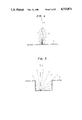
- FIG. 2 shows a model of image when micro-vickers printing, i.e., indentations in square pyramid shapes, is observed with SEM.
- a detector is positioned on the right side in the figure.
- the angle of the incident electron beam to the 4 sides of the indentation is the same but the brightness is different.
- a shadowless illumination concept that no shadow is generated as an electric field is applied to the secondary electron 3 and is being discharged when the incident electron beam 1 discharged from the electron gun 5 as shown in FIG. 3 enters the sample 2 and the secondary electron 3 is collected with the detector 6 has been prevailing for SEM so far.
- this is equivalent to the fact that, as is shown in FIG.
- FIG. 2 indicates that the above concept of the shadowless illumination should be changed.
- the effect of the shadow in SEM images should be considered when determining at what rate electrons discharged from the surface reach the detector from each place.
- the effect of the electric field applied is supposedly not large and the effect of the shadow is important.
- the effect of the shadow reflects the three-dimensional structure such as the depth of holes, shape of opening of holes, etc.
- the basic principle of the embodiment makes use of the effect of a shadow which has been used little so far.
- the brightness and variation of the brightness of the holes, grooves, etc. vary depending on the depth.
- the depth can be obtained.
- a method to collect data on the depth measured by cutting samples and the brightness distribution obtained by observing the samples from above and a method to calculate theoretically are available.
- FIG. 6 is a sectional view of a groove. Taking the horizontal direction as the abscissa and the vertical direction as the ordinate, the groove width of the sample 2 is L and the depth is d.
- the rate of electrons which go out of the groove, f g (x) is expressed by the following equations. ##EQU1## FIG.
- FIG. 7 is a bird's-eye view of a hole with an opening of a rectangle with the side length of Lx and Ly, respectively, and the depth d and the coordinate system for it
- FIG. 8 is a bird's-eye view of a wall with a level difference of d and the coordinate system for it.
- the rate of electrons discharged which reach the detector, f h (x,y) and f.sub. ⁇ (x), respectively, for FIG. 7 and FIG. 8 is described as follows.
- FIG. 9 is a bird's-eye view of a hole with any opening contour and a coordinate system for it. As in the cases in FIGS.
- FIG. 10(a) is a sectional view of the groove which was explained referring to FIG. 6 and FIG. 10(b) is an equivalent line profile of the SEM corresponding to it.
- conspicuous peak 102 is observed, which is not described here.
- the bottom of the groove it is bright at the center and dark at corners.
- the depth can be obtained by measuring the curvature of the line profile at the center of the groove and obtaining its relation to the depth. It is also possible to know the depth by obtaining the relation between the brightness on the outside and the one at the center of the groove, for example, beforehand instead of connecting the depth and brightness by the theoretical consideration as described above.
- FIG. 11 is a block diagram of a hardware composition for this embodiment.
- the electron beam 1 discharged from the electron gun 5 in the SEM system 14 is converged and deflected by the electron lens system 13 and scans the surface of the sample 2 on the sample table 15. Accordingly, the secondary electrons 3 are discharged and detected by the detector 6.
- the detected signal is indicated on the display 16 as it is or after undergoing a proper noise removal treatment by the computer 17.
- the computer 17 processes the signal sent from the detector 6 and, according to the instructions of the key board 18, produces information on depth and indicates it on the display 16.
- FIG. 12 is a flowchart to show the processing procedure of this embodiment, though it is limited to the groove depth. In this figure, the operator moves the field of view to the area interested first at the step 19.
- the image is processed and then it is selected whether the depth is measured or not.
- the line profile at the area of interest is memorized and at the step 23, the groove width is measured from the memorized line profile. From this line profile and groove width value, the depth is calculated at the step 24 and the result is displayed at the step 25.
- depth measurement free from noise is possible by the image processing for improving picture quality.
- the depth of holes, grooves, etc. can be obtained by observing them from above and therefore the depth measurement is possible even if the sample table has no rotating function. Also, this method has such an advantage that deep holes and grooves for which measurement was impossible before can be measured.
- FIG. 14 shows a type of generation of the secondary electron in a SEM.
- the incident electron 205 generates the secondary electron while repeating dispersion in the solid sample and expanding to the diffusion domain 206 after incidence.
- the secondary electron has an energy less than 50 eV usually and therefore only those generated in the layer 207 up to several tens of A below the sample surface can go out of the sample surface. Residual electrons are absorbed in the sample. From this, the discharged secondary electrons are those generated at the common area 208 of the diffusion domain 206 and layer 207.
- the sizes of the secondary electron signals in SEM can be described qualitatively by such a concept. Especially in cases such as in FIG.
- the secondary electrons are generated not only on the top surface of the sample, but also from the layer near the side. Also the secondary electrons are generated from the surface below the level difference by the incident electrons after passing through the sample and going out of the side surface. When the electrons enter near the edge, many secondary electrons are generated and the area near the edge looks bright in the SEM image. This effect is known as an edge effect.
- the basic principle of this embodiment was obtained by applying the above concept to the VLSI surface after the side-etching. In FIG. 14(c), the common area 208 of the diffusion domain 206 and layer 207 of the incident electron 205 becomes larger with the side-etching surface added also in addition to the edge in FIG. 14(b).
- FIGS. 15(a)-(c) show the SEM images when the side-etching magnitude varies.
- the concept of the relation between the width l of the bright band 210 and x in FIG. 15 is shown in FIG. 16. This relation depends on the materials of samples, accelerating voltage of electrons, etc. and can be obtained theoretically also.
- the side-etching magnitude can be presumed only from the observation from above by actually cutting a sample and obtaining the relation between the side-etching magnitude and width of the bright band, or the SEM signals corresponding to 1 scanning experimentally.
- FIG. 17 shows an example of the hardware composition for side-etching amount measurement.
- a VLSI to be measured is placed on the sample table 215 and observed by the electron beam 205 discharged from the body tube 223 of SEM.
- the secondary electron generated by the incidence of electron beam 205 formed with the electron gun 211, converging lens 212, scanning coil 213, and object lens 214 has a directional property when discharged and is therefore measured with the sensors 216 and 217 from 2 directions. These signals are converted to a voltage with the current-voltage converter 218 and detected as a total signal and difference signal with the inverter 219 and adder 220 when necessary.
- the scanning coil 213 is synchronized with the brightness modulation signals on the display 222, thus producing SEM images.
- the side-etching magnitude is presumed from this value of the width of the bright band using the relation between the width of the bright band and side-etching magnitude which was determined beforehand using a cut sample.
- the side-etching magnitude is presumed by storing SEM scanning signals of 1 line which was obtained by measuring a cut sample in the computer 221 shown in FIG. 17 and matching them as a template with measured signals. As described above, the side-etching magnitude can be presumed non-destructively and at high speed according to this embodiment.
- This method can use a normal SEM economically.
Landscapes
- Physics & Mathematics (AREA)
- Chemical & Material Sciences (AREA)
- Analytical Chemistry (AREA)
- Electromagnetism (AREA)
- General Physics & Mathematics (AREA)
- Length-Measuring Devices Using Wave Or Particle Radiation (AREA)
Abstract
Description
Claims (3)
Applications Claiming Priority (4)
| Application Number | Priority Date | Filing Date | Title |
|---|---|---|---|
| JP60-80130 | 1985-04-17 | ||
| JP60080130A JPS61239107A (en) | 1985-04-17 | 1985-04-17 | Depth measuring system |
| JP60-80129 | 1985-04-17 | ||
| JP60080129A JPS61239634A (en) | 1985-04-17 | 1985-04-17 | Measuring system for amount of side etching |
Publications (1)
| Publication Number | Publication Date |
|---|---|
| US4733074A true US4733074A (en) | 1988-03-22 |
Family
ID=26421186
Family Applications (1)
| Application Number | Title | Priority Date | Filing Date |
|---|---|---|---|
| US06/852,741 Expired - Lifetime US4733074A (en) | 1985-04-17 | 1986-04-16 | Sample surface structure measuring method |
Country Status (1)
| Country | Link |
|---|---|
| US (1) | US4733074A (en) |
Cited By (22)
| Publication number | Priority date | Publication date | Assignee | Title |
|---|---|---|---|---|
| US4835385A (en) * | 1986-07-25 | 1989-05-30 | Hitachi, Ltd. | Method of measuring sectional shape and a system therefor |
| US5028780A (en) * | 1988-12-01 | 1991-07-02 | Seiko Instruments, Inc. | Preparation and observation method of micro-section |
| US5412210A (en) * | 1990-10-12 | 1995-05-02 | Hitachi, Ltd. | Scanning electron microscope and method for production of semiconductor device by using the same |
| US5458731A (en) * | 1994-02-04 | 1995-10-17 | Fujitsu Limited | Method for fast and non-destructive examination of etched features |
| US5528033A (en) * | 1995-03-29 | 1996-06-18 | International Business Machines Corporation | Automatic surface profiling for submicron device |
| US5594245A (en) * | 1990-10-12 | 1997-01-14 | Hitachi, Ltd. | Scanning electron microscope and method for dimension measuring by using the same |
| US5780852A (en) * | 1996-03-25 | 1998-07-14 | Texas Instruments Incorporated | Dimension measurement of a semiconductor device |
| US5798529A (en) * | 1996-05-28 | 1998-08-25 | International Business Machines Corporation | Focused ion beam metrology |
| US5866904A (en) * | 1990-10-12 | 1999-02-02 | Hitachi, Ltd. | Scanning electron microscope and method for dimension measuring by using the same |
| US6054710A (en) * | 1997-12-18 | 2000-04-25 | Cypress Semiconductor Corp. | Method and apparatus for obtaining two- or three-dimensional information from scanning electron microscopy |
| US6140655A (en) * | 1995-04-13 | 2000-10-31 | North Carolina State University | Method for water vapor enhanced charged-particle-beam machining |
| US6472662B1 (en) * | 2000-08-30 | 2002-10-29 | International Business Machines Corporation | Automated method for determining several critical dimension properties from scanning electron microscope by using several tilted beam or sample scans |
| US6538249B1 (en) * | 1999-07-09 | 2003-03-25 | Hitachi, Ltd. | Image-formation apparatus using charged particle beams under various focus conditions |
| US6627887B1 (en) * | 2000-06-20 | 2003-09-30 | Advanced Micro Devices, Inc. | System and method for constructing a profile of a structure in an integrated circuit |
| US6660655B2 (en) | 1999-10-12 | 2003-12-09 | Taiwan Semiconductor Manufacturing Company | Method and solution for preparing SEM samples for low-K materials |
| US6738503B1 (en) * | 1999-08-27 | 2004-05-18 | Renesas Technology Corp. | Notch inspection apparatus and method based on shading pattern matching |
| US20050056793A1 (en) * | 1998-12-01 | 2005-03-17 | Hiroshi Fudoji | Process for precise arrangement of micro-bodies |
| US20130248706A1 (en) * | 2012-03-26 | 2013-09-26 | Haruko Akutsu | Sample analyzing apparatus and sample analyzing method |
| CN104406537A (en) * | 2014-12-05 | 2015-03-11 | 重庆材料研究院有限公司 | Method for measuring micron-order depths of pits of component |
| US20190378679A1 (en) * | 2018-06-06 | 2019-12-12 | Hitachi High-Technologies Corporation | Pattern Measuring Method, Pattern Measuring Tool and Computer Readable Medium |
| CN111640375A (en) * | 2019-07-24 | 2020-09-08 | 友达光电股份有限公司 | Flexible display device |
| CN112635342A (en) * | 2019-09-24 | 2021-04-09 | 应用材料公司 | Use of an electron beam scanning electron microscope for characterizing a sidewall obscured from view by an electron beam |
Citations (8)
| Publication number | Priority date | Publication date | Assignee | Title |
|---|---|---|---|---|
| US3329813A (en) * | 1964-08-25 | 1967-07-04 | Jeol Ltd | Backscatter electron analysis apparatus to determine elemental content or surface topography of a specimen |
| US3597607A (en) * | 1967-02-16 | 1971-08-03 | Cambridge Instr Co | Electron probe employing three secondary emission detectors whose outputs are combined to minimize error |
| US3876879A (en) * | 1973-11-09 | 1975-04-08 | Calspan Corp | Method and apparatus for determining surface characteristics incorporating a scanning electron microscope |
| US4221965A (en) * | 1977-08-23 | 1980-09-09 | Hitachi, Ltd. | Scanning type electron microscope |
| JPS5954160A (en) * | 1982-09-22 | 1984-03-28 | Jeol Ltd | Charged corpuscular ray device |
| JPS60741A (en) * | 1983-06-16 | 1985-01-05 | Toshiba Mach Co Ltd | Exposure by electron beam |
| WO1985004250A1 (en) * | 1984-03-20 | 1985-09-26 | Nixon, Larry, Sheldon | Method and apparatus for precision sem measurements |
| US4556797A (en) * | 1982-09-09 | 1985-12-03 | Hitachi, Ltd. | Method and apparatus for detecting edge of fine pattern on specimen |
-
1986
- 1986-04-16 US US06/852,741 patent/US4733074A/en not_active Expired - Lifetime
Patent Citations (8)
| Publication number | Priority date | Publication date | Assignee | Title |
|---|---|---|---|---|
| US3329813A (en) * | 1964-08-25 | 1967-07-04 | Jeol Ltd | Backscatter electron analysis apparatus to determine elemental content or surface topography of a specimen |
| US3597607A (en) * | 1967-02-16 | 1971-08-03 | Cambridge Instr Co | Electron probe employing three secondary emission detectors whose outputs are combined to minimize error |
| US3876879A (en) * | 1973-11-09 | 1975-04-08 | Calspan Corp | Method and apparatus for determining surface characteristics incorporating a scanning electron microscope |
| US4221965A (en) * | 1977-08-23 | 1980-09-09 | Hitachi, Ltd. | Scanning type electron microscope |
| US4556797A (en) * | 1982-09-09 | 1985-12-03 | Hitachi, Ltd. | Method and apparatus for detecting edge of fine pattern on specimen |
| JPS5954160A (en) * | 1982-09-22 | 1984-03-28 | Jeol Ltd | Charged corpuscular ray device |
| JPS60741A (en) * | 1983-06-16 | 1985-01-05 | Toshiba Mach Co Ltd | Exposure by electron beam |
| WO1985004250A1 (en) * | 1984-03-20 | 1985-09-26 | Nixon, Larry, Sheldon | Method and apparatus for precision sem measurements |
Cited By (39)
| Publication number | Priority date | Publication date | Assignee | Title |
|---|---|---|---|---|
| US4835385A (en) * | 1986-07-25 | 1989-05-30 | Hitachi, Ltd. | Method of measuring sectional shape and a system therefor |
| US5028780A (en) * | 1988-12-01 | 1991-07-02 | Seiko Instruments, Inc. | Preparation and observation method of micro-section |
| US5866904A (en) * | 1990-10-12 | 1999-02-02 | Hitachi, Ltd. | Scanning electron microscope and method for dimension measuring by using the same |
| US5412210A (en) * | 1990-10-12 | 1995-05-02 | Hitachi, Ltd. | Scanning electron microscope and method for production of semiconductor device by using the same |
| US5594245A (en) * | 1990-10-12 | 1997-01-14 | Hitachi, Ltd. | Scanning electron microscope and method for dimension measuring by using the same |
| US6114695A (en) * | 1990-10-12 | 2000-09-05 | Hitachi, Ltd. | Scanning electron microscope and method for dimension measuring by using the same |
| US5969357A (en) * | 1990-10-12 | 1999-10-19 | Hitachi, Ltd. | Scanning electron microscope and method for dimension measuring by using the same |
| US5458731A (en) * | 1994-02-04 | 1995-10-17 | Fujitsu Limited | Method for fast and non-destructive examination of etched features |
| US5528033A (en) * | 1995-03-29 | 1996-06-18 | International Business Machines Corporation | Automatic surface profiling for submicron device |
| US6140655A (en) * | 1995-04-13 | 2000-10-31 | North Carolina State University | Method for water vapor enhanced charged-particle-beam machining |
| US5780852A (en) * | 1996-03-25 | 1998-07-14 | Texas Instruments Incorporated | Dimension measurement of a semiconductor device |
| US5798529A (en) * | 1996-05-28 | 1998-08-25 | International Business Machines Corporation | Focused ion beam metrology |
| US6054710A (en) * | 1997-12-18 | 2000-04-25 | Cypress Semiconductor Corp. | Method and apparatus for obtaining two- or three-dimensional information from scanning electron microscopy |
| US20050056793A1 (en) * | 1998-12-01 | 2005-03-17 | Hiroshi Fudoji | Process for precise arrangement of micro-bodies |
| US7323227B2 (en) | 1998-12-01 | 2008-01-29 | Japan As Represented By Director General Of National Research Institute Of Metals | Process for precise arrangement of micro-bodies |
| US20060231755A1 (en) * | 1998-12-01 | 2006-10-19 | Hiroshi Fudoji | Process for precise arrangement of micro-bodies |
| US20080116376A1 (en) * | 1999-07-09 | 2008-05-22 | Hitachi, Ltd. | Charged particle beam apparatus |
| US7642514B2 (en) | 1999-07-09 | 2010-01-05 | Hitachi, Ltd. | Charged particle beam apparatus |
| US6653633B2 (en) | 1999-07-09 | 2003-11-25 | Hitachi, Ltd. | Charged particle beam apparatus |
| US20050184237A1 (en) * | 1999-07-09 | 2005-08-25 | Hitachi, Ltd. | Charged particle beam apparatus |
| US6936818B2 (en) | 1999-07-09 | 2005-08-30 | Hitachi, Ltd. | Charged particle beam apparatus |
| US7109485B2 (en) | 1999-07-09 | 2006-09-19 | Hitachi, Ltd. | Charged particle beam apparatus |
| US20070023657A1 (en) * | 1999-07-09 | 2007-02-01 | Hitachi, Ltd. | Charged particle beam apparatus |
| US6538249B1 (en) * | 1999-07-09 | 2003-03-25 | Hitachi, Ltd. | Image-formation apparatus using charged particle beams under various focus conditions |
| US7329868B2 (en) | 1999-07-09 | 2008-02-12 | Hitachi, Ltd. | Charged particle beam apparatus |
| US6738503B1 (en) * | 1999-08-27 | 2004-05-18 | Renesas Technology Corp. | Notch inspection apparatus and method based on shading pattern matching |
| US6660655B2 (en) | 1999-10-12 | 2003-12-09 | Taiwan Semiconductor Manufacturing Company | Method and solution for preparing SEM samples for low-K materials |
| US6627887B1 (en) * | 2000-06-20 | 2003-09-30 | Advanced Micro Devices, Inc. | System and method for constructing a profile of a structure in an integrated circuit |
| US6472662B1 (en) * | 2000-08-30 | 2002-10-29 | International Business Machines Corporation | Automated method for determining several critical dimension properties from scanning electron microscope by using several tilted beam or sample scans |
| US20130248706A1 (en) * | 2012-03-26 | 2013-09-26 | Haruko Akutsu | Sample analyzing apparatus and sample analyzing method |
| US8748844B2 (en) * | 2012-03-26 | 2014-06-10 | Kabushiki Kaisha Toshiba | Sample analyzing apparatus and sample analyzing method |
| CN104406537A (en) * | 2014-12-05 | 2015-03-11 | 重庆材料研究院有限公司 | Method for measuring micron-order depths of pits of component |
| CN104406537B (en) * | 2014-12-05 | 2017-03-01 | 重庆材料研究院有限公司 | The method of measurement part pit micrometer level depth |
| US20190378679A1 (en) * | 2018-06-06 | 2019-12-12 | Hitachi High-Technologies Corporation | Pattern Measuring Method, Pattern Measuring Tool and Computer Readable Medium |
| US10903041B2 (en) * | 2018-06-06 | 2021-01-26 | Hitachi High-Tech Corporation | Pattern measuring method, pattern measuring tool and computer readable medium |
| TWI744644B (en) * | 2018-06-06 | 2021-11-01 | 日商日立全球先端科技股份有限公司 | Pattern measuring method, pattern measuring tool, and computer readable medium |
| CN111640375A (en) * | 2019-07-24 | 2020-09-08 | 友达光电股份有限公司 | Flexible display device |
| CN112635342A (en) * | 2019-09-24 | 2021-04-09 | 应用材料公司 | Use of an electron beam scanning electron microscope for characterizing a sidewall obscured from view by an electron beam |
| CN112635342B (en) * | 2019-09-24 | 2023-08-15 | 应用材料公司 | Use of an electron beam scanning electron microscope for characterizing a sidewall that is blocked from view by an electron beam |
Similar Documents
| Publication | Publication Date | Title |
|---|---|---|
| US4733074A (en) | Sample surface structure measuring method | |
| US5438413A (en) | Process for measuring overlay misregistration during semiconductor wafer fabrication | |
| EP0244781B1 (en) | Method and apparatus of using a two beam interference microscope for inspection of integrated circuits and the like | |
| US6353222B1 (en) | Determining defect depth and contour information in wafer structures using multiple SEM images | |
| EP0345772B1 (en) | Pattern configuration measuring apparatus | |
| JP3959355B2 (en) | Measuring method of three-dimensional shape of fine pattern | |
| EP0641020A2 (en) | Multiple-scan method for wafer particle analysis | |
| US5159643A (en) | Method and apparatus for measuring pattern dimension | |
| US4725730A (en) | System of automatically measuring sectional shape | |
| EP0312083B1 (en) | Pattern measurement method | |
| US5161201A (en) | Method of and apparatus for measuring pattern profile | |
| WO1998054612A1 (en) | High speed, high detection sensitivity inspection of repetitive and random specimen patterns | |
| US7209596B2 (en) | Method of precision calibration of a microscope and the like | |
| US4835402A (en) | Method for quantitatively determining the shape of small size protruding patterns | |
| Vartanian et al. | TSV reveal height and dimension metrology by the TSOM method | |
| JPH0445047B2 (en) | ||
| US4556797A (en) | Method and apparatus for detecting edge of fine pattern on specimen | |
| JP2701764B2 (en) | Apparatus and method for measuring size of charged particle beam | |
| Ammann et al. | Characterization of self-affine surfaces from 3D digital reconstruction | |
| Lindow et al. | Scanned laser imaging for integrated circuit metrology | |
| JPS61239107A (en) | Depth measuring system | |
| Lorincik et al. | Scanning scattering microscope for surface microtopography and defect imaging | |
| Wells et al. | Top-down topography of deeply etched silicon in the scanning electron microscope | |
| Komatsu et al. | Measurement of geometrical dimensions using scanning electron microscopy | |
| Breton et al. | A contactless 3-D measuring technique for IC inspection |
Legal Events
| Date | Code | Title | Description |
|---|---|---|---|
| AS | Assignment |
Owner name: HITACHI, LTD., 6, KANDA SURUGADAI 4-CHOME, CHIYODA Free format text: ASSIGNMENT OF ASSIGNORS INTEREST.;ASSIGNORS:KATO, MAKOTO;YOKOYAMA, TETSUO;ARIMA, JYUNTARO;AND OTHERS;REEL/FRAME:004766/0367 Effective date: 19860317 Owner name: HITACHI, LTD., A CORP. OF JAPAN,JAPAN Free format text: ASSIGNMENT OF ASSIGNORS INTEREST;ASSIGNORS:KATO, MAKOTO;YOKOYAMA, TETSUO;ARIMA, JYUNTARO;AND OTHERS;REEL/FRAME:004766/0367 Effective date: 19860317 |
|
| STCF | Information on status: patent grant |
Free format text: PATENTED CASE |
|
| FPAY | Fee payment |
Year of fee payment: 4 |
|
| FEPP | Fee payment procedure |
Free format text: PAYOR NUMBER ASSIGNED (ORIGINAL EVENT CODE: ASPN); ENTITY STATUS OF PATENT OWNER: LARGE ENTITY |
|
| FPAY | Fee payment |
Year of fee payment: 8 |
|
| FPAY | Fee payment |
Year of fee payment: 12 |