US4726035A - Analog/digital adaptive line enhancer - Google Patents
Analog/digital adaptive line enhancer Download PDFInfo
- Publication number
- US4726035A US4726035A US07/030,301 US3030187A US4726035A US 4726035 A US4726035 A US 4726035A US 3030187 A US3030187 A US 3030187A US 4726035 A US4726035 A US 4726035A
- Authority
- US
- United States
- Prior art keywords
- signal
- analog
- mixing
- adaptive
- local oscillator
- Prior art date
- Legal status (The legal status is an assumption and is not a legal conclusion. Google has not performed a legal analysis and makes no representation as to the accuracy of the status listed.)
- Expired - Lifetime
Links
Images
Classifications
-
- H—ELECTRICITY
- H03—ELECTRONIC CIRCUITRY
- H03H—IMPEDANCE NETWORKS, e.g. RESONANT CIRCUITS; RESONATORS
- H03H21/00—Adaptive networks
- H03H21/0001—Analogue adaptive filters
Definitions
- Both digital and analog adaptive line enhancers act as narrowband filters to enhance the narrowband frequency components present in a broadband noise field.
- Adaptive line enhancers are constructed so that they automatically adjust to variations in the input signal in order to provide a least mean square (LMS) approximation of a WienerHopf filter.
- LMS least mean square
- WienerHopf filter This device uses a number of stored weight values which are continuously adjusted so that the device automatically filters out the components of the signal which are not correlated in time in order to pass correlated stable spectral lines.
- the present invention provides a digital adaptive processor which operates with analog signals that are supplied on the reference and the error feedback channels and which provides an analog narrowband channel output signal.
- the invention includes up/down conversion, and lowpass and bandpass filtering in order to process any preset frequency band.
- adaptive line enhancers may be extended to frequency bands beyond the range of currently available digital components, while retaining the advantages of digital adaptive processors.
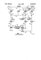
- FIGURE shows a block diagram of an analog/digital adaptive line enhancer constructed in accordance with the present invention.
- the adaptive line enhancer 10 receives an analog input signal on the line 12. This signal is passed on the line 14 which is labeled "ANALOG CHANNEL" to the non-inverting input of an analog summer.
- the Analog signal on the line 14 contains both wideband and narrowband components.
- the WIDEBAND CHANNEL output signal is supplied by the analog summer 16 on the output line 18 after the NARROWBAND CHANNEL signal has been subtracted from the ANALOG CHANNEL signal in the analog summer due to the application of the NARROWBAND CHANNEL signal to the inverting input terminal of the analog summer 16.
- the analog input signal is coupled on the line 20 to a bandpass filter 22.
- the output of the bandpass filter 22 is coupled on the line 24 to a mixer, or signal multiplier, 26.
- Another input of the multiplier 26 receives the output of a stable local oscillator 28 on the line 30.
- the bandpass filter 22 is ideally constructed so that it passes a flatband of signals, with the frequency of the local oscillator being at the lowermost end of the frequency band.
- the output of the mixer supplied on the line 32 contains the mixed signals supplied by the bandpass filter which extends from the local oscillator frequency to the upper frequency of the present frequency band to be processed by the adaptive filter.
- the lowpass filter 34 which receives the signal on the line 32 ideally will pass signals on the line 36 to the analog/digital converter 38 from D.C. to a frequency which is well below that of the local oscillator.
- the power tapped from the input signal is bandpass filtered and down converted to baseband.
- a lowpass filter is then used to further restrict the bandwidth of the mixed reference signal to the Nyquist frequency of the digital adaptive filter.
- the digital output of the A/D converter 38 is supplied on the line 40 to the adaptive filter 42.
- an adaptive filter there are a number of weight accumulators which store weight values.
- the signal from the A/D converter is supplied through a decorrelation delay to a number of taps of a tapped delay line.
- the digital NARROWBAND CHANNEL signal of the adaptive filter is provided on the line 44 to a digital/analog output converter 46.
- the output of the D/A converter 46 is supplied on the line 48 to derive the narrowband signal. While the delay may be adjusted in an integral number of clock cycles by adding more taps and by shifting the narrowband output taps from the weight update taps, it may be found that the time delay through the feedback loop is not exactly an integral number of clock cycles.
- Adjustments for time variations less than one clock cycle period may be provided by relative timing differences between clock ⁇ 1 for D/A converter 46 and clock ⁇ 2 for A/D converter 38. For example, this may be done by triggering the A/D converter 38 off of the rising edges of clock ⁇ 1 and ⁇ 2 triggering the D/A converter 46 off of the following edges of clock ⁇ 2 wherein clock ⁇ 2 is delayed in time from clock ⁇ 1 sufficiently to provide the appropriate timing adjustment. For example, if it is assumed that the actual delay through the feedback loop is 2.7 clock cycles, and three additional taps have been added to provide three additional clock delay cycles in triggering the D/A converter 46, then the timing of the A/D converter 38 will be early by 0.3 clock cycles. This 0.3 clock cycle difference may be adjusted by controlling the timing of the D/A converter 46 and the A/D converters 38 and 50.
- the NARROWBAND CHANNEL signal on line 48 is supplied to the lowpass filter 51 which is used to eliminate the high frequency transition components from the D/A converters.
- the signal is then passed on line 52 to the mixer 54.
- the mixer 54 receives the local oscillator signal on the line 56 and the NARROWBAND CHANNEL mixed output signal is supplied on the line 58 to the bandpass filter 60.
- the output of the bandpass filter 60 is supplied on the line 62 to the inverting input terminal of the analog summer 16.
- the bandpass filter 60 is used to eliminate the lower sideband generated by the up conversion that occurred at the mixer 54.
- the NARROWBAND CHANNEL output may be supplied on the line 64.
- the error signal to update the accumulator weights is split off from the WIDEBAND CHANNEL on the line 66 through the bandpass filter 68.
- the signal on the line 66 is passed through bandpass filter 68 to the line 70.
- the bandpass filter 68 has a frequency band identical to that of the bandpass filter 22 so that its band extends at the lower end from the frequency of the local oscillator to a higher frequency.
- the output of the bandpass filter is supplied on the line 70 to the mixer 72 which also receives the local oscillator signal on line 74.
- the mixer 72 receives the local oscillator signal on line 74.
- the resulting signal is supplied on the line 76 of the FEEDBACK CHANNEL.
- the lowpass filter 78 like the lowpass filter 34, is constructed to pass a flatband from D.C. to a frequency well below the local oscillator frequency.
- the lowpass filters 34 and 78 in both the reference and error feedback channels are used to band limit the reference and error feedback signals to the Nyquist rate of the digital adaptive processor.
- the digitized output of the A/D converter 50 is supplied to the adaptive filter 42 as an error signal which controls the updating of the weights of the adaptive filter 42.
- adaptive line enhancer of the present invention in which analog components are utilized, to allow the narrowband interference to be directly subtracted from the input signal without further distortion being introduced.
- This adaptive line enhancer also represents a constant group delay to the input signal which is important to communication applications.
Landscapes
- Analogue/Digital Conversion (AREA)
- Filters That Use Time-Delay Elements (AREA)
- Noise Elimination (AREA)
Abstract
Description
Claims (4)
Priority Applications (6)
| Application Number | Priority Date | Filing Date | Title |
|---|---|---|---|
| US07/030,301 US4726035A (en) | 1987-03-26 | 1987-03-26 | Analog/digital adaptive line enhancer |
| DE8888903539T DE3867005D1 (en) | 1987-03-26 | 1988-03-14 | ANALOG / DIGITAL ADAPTIVE LINE EQUALIZER. |
| PCT/US1988/000784 WO1988007789A1 (en) | 1987-03-26 | 1988-03-14 | Analog/digital adaptive line enhancer |
| JP63503179A JPH0716149B2 (en) | 1987-03-26 | 1988-03-14 | Analog / digital adaptive line enhancer |
| EP88903539A EP0307455B1 (en) | 1987-03-26 | 1988-03-14 | Analog/digital adaptive line enhancer |
| CA000562589A CA1285999C (en) | 1987-03-26 | 1988-03-25 | Analog/digital adaptive line enhancer |
Applications Claiming Priority (1)
| Application Number | Priority Date | Filing Date | Title |
|---|---|---|---|
| US07/030,301 US4726035A (en) | 1987-03-26 | 1987-03-26 | Analog/digital adaptive line enhancer |
Publications (1)
| Publication Number | Publication Date |
|---|---|
| US4726035A true US4726035A (en) | 1988-02-16 |
Family
ID=21853554
Family Applications (1)
| Application Number | Title | Priority Date | Filing Date |
|---|---|---|---|
| US07/030,301 Expired - Lifetime US4726035A (en) | 1987-03-26 | 1987-03-26 | Analog/digital adaptive line enhancer |
Country Status (6)
| Country | Link |
|---|---|
| US (1) | US4726035A (en) |
| EP (1) | EP0307455B1 (en) |
| JP (1) | JPH0716149B2 (en) |
| CA (1) | CA1285999C (en) |
| DE (1) | DE3867005D1 (en) |
| WO (1) | WO1988007789A1 (en) |
Cited By (7)
| Publication number | Priority date | Publication date | Assignee | Title |
|---|---|---|---|---|
| US4788652A (en) * | 1987-03-26 | 1988-11-29 | Unisys Corporation | I-Q channel adaptive line enhancer |
| EP0496797A1 (en) * | 1989-10-16 | 1992-08-05 | Noise Cancellation Technologies, Inc. | In-wire selective cancellation system |
| US5210712A (en) * | 1990-09-29 | 1993-05-11 | Anritsu Corporation | Waveform shaping circuit and digital signal analyzing apparatus using the same |
| US5263191A (en) * | 1991-12-11 | 1993-11-16 | Westinghouse Electric Corp. | Method and circuit for processing and filtering signals |
| US5272663A (en) * | 1992-05-05 | 1993-12-21 | The Board Of Trustees Of The University Of Illinois | Apparatus and method for wide bandwidth adaptive filtering |
| US5428834A (en) * | 1991-12-11 | 1995-06-27 | Xetron Corporation | Method and circuit for processing and filtering signals |
| US20050249273A1 (en) * | 2004-05-05 | 2005-11-10 | Ashley Jonathan J | Method and apparatus for generating filter tap weights and biases for signal dependent branch metric computation |
Citations (4)
| Publication number | Priority date | Publication date | Assignee | Title |
|---|---|---|---|---|
| US4236224A (en) * | 1978-12-26 | 1980-11-25 | Rockwell International Corporation | Low roundoff noise digital filter |
| US4238746A (en) * | 1978-03-20 | 1980-12-09 | The United States Of America As Represented By The Secretary Of The Navy | Adaptive line enhancer |
| US4266204A (en) * | 1979-09-04 | 1981-05-05 | Sperry Rand Corporation | Delay line signal equalizer for magnetic recording signal detection circuits |
| US4351060A (en) * | 1980-10-23 | 1982-09-21 | International Telephone And Telegraph Corporation | Automatic, digitally synthesized matching line terminating impedance |
Family Cites Families (3)
| Publication number | Priority date | Publication date | Assignee | Title |
|---|---|---|---|---|
| US4791390A (en) * | 1982-07-01 | 1988-12-13 | Sperry Corporation | MSE variable step adaptive filter |
| DE3417776A1 (en) * | 1983-06-01 | 1985-11-21 | Manfred Dipl.-Ing. 7000 Stuttgart Horn | Method and circuit arrangements for cancelling non-linear amplitude and/or phase distortions |
| GB2187064B (en) * | 1986-02-21 | 1990-01-31 | Stc Plc | Adaptive filter |
-
1987
- 1987-03-26 US US07/030,301 patent/US4726035A/en not_active Expired - Lifetime
-
1988
- 1988-03-14 EP EP88903539A patent/EP0307455B1/en not_active Expired - Lifetime
- 1988-03-14 WO PCT/US1988/000784 patent/WO1988007789A1/en active IP Right Grant
- 1988-03-14 JP JP63503179A patent/JPH0716149B2/en not_active Expired - Lifetime
- 1988-03-14 DE DE8888903539T patent/DE3867005D1/en not_active Expired - Fee Related
- 1988-03-25 CA CA000562589A patent/CA1285999C/en not_active Expired - Fee Related
Patent Citations (4)
| Publication number | Priority date | Publication date | Assignee | Title |
|---|---|---|---|---|
| US4238746A (en) * | 1978-03-20 | 1980-12-09 | The United States Of America As Represented By The Secretary Of The Navy | Adaptive line enhancer |
| US4236224A (en) * | 1978-12-26 | 1980-11-25 | Rockwell International Corporation | Low roundoff noise digital filter |
| US4266204A (en) * | 1979-09-04 | 1981-05-05 | Sperry Rand Corporation | Delay line signal equalizer for magnetic recording signal detection circuits |
| US4351060A (en) * | 1980-10-23 | 1982-09-21 | International Telephone And Telegraph Corporation | Automatic, digitally synthesized matching line terminating impedance |
Cited By (9)
| Publication number | Priority date | Publication date | Assignee | Title |
|---|---|---|---|---|
| US4788652A (en) * | 1987-03-26 | 1988-11-29 | Unisys Corporation | I-Q channel adaptive line enhancer |
| EP0496797A1 (en) * | 1989-10-16 | 1992-08-05 | Noise Cancellation Technologies, Inc. | In-wire selective cancellation system |
| EP0496797A4 (en) * | 1989-10-16 | 1993-12-15 | Noise Cancellation Technologies, Inc. | In-wire selective cancellation system |
| US5210712A (en) * | 1990-09-29 | 1993-05-11 | Anritsu Corporation | Waveform shaping circuit and digital signal analyzing apparatus using the same |
| US5263191A (en) * | 1991-12-11 | 1993-11-16 | Westinghouse Electric Corp. | Method and circuit for processing and filtering signals |
| US5428834A (en) * | 1991-12-11 | 1995-06-27 | Xetron Corporation | Method and circuit for processing and filtering signals |
| US5272663A (en) * | 1992-05-05 | 1993-12-21 | The Board Of Trustees Of The University Of Illinois | Apparatus and method for wide bandwidth adaptive filtering |
| US20050249273A1 (en) * | 2004-05-05 | 2005-11-10 | Ashley Jonathan J | Method and apparatus for generating filter tap weights and biases for signal dependent branch metric computation |
| US8223827B2 (en) * | 2004-05-05 | 2012-07-17 | Agere Systems Inc. | Method and apparatus for generating filter tap weights and biases for signal dependent branch metric computation |
Also Published As
| Publication number | Publication date |
|---|---|
| CA1285999C (en) | 1991-07-09 |
| EP0307455B1 (en) | 1991-12-18 |
| EP0307455A1 (en) | 1989-03-22 |
| JPH02501789A (en) | 1990-06-14 |
| JPH0716149B2 (en) | 1995-02-22 |
| DE3867005D1 (en) | 1992-01-30 |
| WO1988007789A1 (en) | 1988-10-06 |
Similar Documents
| Publication | Publication Date | Title |
|---|---|---|
| CA2277756C (en) | Flexible and programmable delta-sigma analog signal converter | |
| US4890107A (en) | Analogue-to-digital converter | |
| US5617090A (en) | Multi-channel sigma-delta A/D converters with improved throughput | |
| US7046749B2 (en) | Narrowband gain control of receiver with digital post filtering | |
| US5892472A (en) | Processor controlled analog-to-digital converter circuit | |
| US4649507A (en) | Segmented transversal filter | |
| MXPA04012483A (en) | Method and system for all digital gain control. | |
| US5798724A (en) | Interpolating digital to analog converter architecture for improved spurious signal suppression | |
| US5561660A (en) | Offset and phase correction for delta-sigma modulators | |
| US4726035A (en) | Analog/digital adaptive line enhancer | |
| US4843390A (en) | Oversampled A/D converter having digital error correction | |
| GB2233518A (en) | Analogue to digital converters | |
| US6097443A (en) | Method and arrangement for the analog/digital conversion of a picture signal | |
| US4547888A (en) | Recursive adaptive equalizer for SMSK data links | |
| US4726036A (en) | Digital adaptive filter for a high throughput digital adaptive processor | |
| KR850000140B1 (en) | Subscriber line audio processing circuit apparatus | |
| US4983975A (en) | A/D converter | |
| US4963881A (en) | Method and apparatus for enhancing the signal resolution of an analog-to-digital converter | |
| US5555272A (en) | Signal processing device using several different filterings, especially for audio-frequency coding of voice signals | |
| US4788652A (en) | I-Q channel adaptive line enhancer | |
| JPH04291822A (en) | A/d converter | |
| US11611350B2 (en) | Analog-to-digital converter, wireless communication apparatus, and analog-to-digital conversion method | |
| JPH01103013A (en) | Digital clip circuit | |
| JPS6367888A (en) | Automatic digital color control circuit | |
| JPS57160220A (en) | Analog to digital converter |
Legal Events
| Date | Code | Title | Description |
|---|---|---|---|
| AS | Assignment |
Owner name: UNISYS CORPORATION, P.O. BOX 500, BLUE BELL, PENNS Free format text: ASSIGNMENT OF ASSIGNORS INTEREST.;ASSIGNORS:BULLOCK, SCOTT R.;SMITH, PATRICK J.;REEL/FRAME:004791/0502 Effective date: 19870312 Owner name: UNISYS CORPORATION, P.O. BOX 500, BLUE BELL, PENNS Free format text: ASSIGNMENT OF ASSIGNORS INTEREST;ASSIGNORS:BULLOCK, SCOTT R.;SMITH, PATRICK J.;REEL/FRAME:004791/0502 Effective date: 19870312 |
|
| STCF | Information on status: patent grant |
Free format text: PATENTED CASE |
|
| FPAY | Fee payment |
Year of fee payment: 4 |
|
| FEPP | Fee payment procedure |
Free format text: PAYOR NUMBER ASSIGNED (ORIGINAL EVENT CODE: ASPN); ENTITY STATUS OF PATENT OWNER: LARGE ENTITY |
|
| FPAY | Fee payment |
Year of fee payment: 8 |
|
| FPAY | Fee payment |
Year of fee payment: 12 |