US4724611A - Method for producing semiconductor module - Google Patents
Method for producing semiconductor module Download PDFInfo
- Publication number
- US4724611A US4724611A US06/898,428 US89842886A US4724611A US 4724611 A US4724611 A US 4724611A US 89842886 A US89842886 A US 89842886A US 4724611 A US4724611 A US 4724611A
- Authority
- US
- United States
- Prior art keywords
- heat
- conductive material
- chamber
- substrate
- holding member
- Prior art date
- Legal status (The legal status is an assumption and is not a legal conclusion. Google has not performed a legal analysis and makes no representation as to the accuracy of the status listed.)
- Expired - Fee Related
Links
Images

Classifications
-
- H—ELECTRICITY
- H01—ELECTRIC ELEMENTS
- H01L—SEMICONDUCTOR DEVICES NOT COVERED BY CLASS H10
- H01L21/00—Processes or apparatus adapted for the manufacture or treatment of semiconductor or solid state devices or of parts thereof
- H01L21/02—Manufacture or treatment of semiconductor devices or of parts thereof
- H01L21/04—Manufacture or treatment of semiconductor devices or of parts thereof the devices having at least one potential-jump barrier or surface barrier, e.g. PN junction, depletion layer or carrier concentration layer
- H01L21/50—Assembly of semiconductor devices using processes or apparatus not provided for in a single one of the subgroups H01L21/06 - H01L21/326, e.g. sealing of a cap to a base of a container
-
- H—ELECTRICITY
- H01—ELECTRIC ELEMENTS
- H01L—SEMICONDUCTOR DEVICES NOT COVERED BY CLASS H10
- H01L23/00—Details of semiconductor or other solid state devices
- H01L23/34—Arrangements for cooling, heating, ventilating or temperature compensation ; Temperature sensing arrangements
- H01L23/42—Fillings or auxiliary members in containers or encapsulations selected or arranged to facilitate heating or cooling
- H01L23/433—Auxiliary members in containers characterised by their shape, e.g. pistons
-
- H—ELECTRICITY
- H01—ELECTRIC ELEMENTS
- H01L—SEMICONDUCTOR DEVICES NOT COVERED BY CLASS H10
- H01L25/00—Assemblies consisting of a plurality of individual semiconductor or other solid state devices ; Multistep manufacturing processes thereof
- H01L25/03—Assemblies consisting of a plurality of individual semiconductor or other solid state devices ; Multistep manufacturing processes thereof all the devices being of a type provided for in the same subgroup of groups H01L27/00 - H01L33/00, or in a single subclass of H10K, H10N, e.g. assemblies of rectifier diodes
- H01L25/04—Assemblies consisting of a plurality of individual semiconductor or other solid state devices ; Multistep manufacturing processes thereof all the devices being of a type provided for in the same subgroup of groups H01L27/00 - H01L33/00, or in a single subclass of H10K, H10N, e.g. assemblies of rectifier diodes the devices not having separate containers
- H01L25/065—Assemblies consisting of a plurality of individual semiconductor or other solid state devices ; Multistep manufacturing processes thereof all the devices being of a type provided for in the same subgroup of groups H01L27/00 - H01L33/00, or in a single subclass of H10K, H10N, e.g. assemblies of rectifier diodes the devices not having separate containers the devices being of a type provided for in group H01L27/00
- H01L25/0655—Assemblies consisting of a plurality of individual semiconductor or other solid state devices ; Multistep manufacturing processes thereof all the devices being of a type provided for in the same subgroup of groups H01L27/00 - H01L33/00, or in a single subclass of H10K, H10N, e.g. assemblies of rectifier diodes the devices not having separate containers the devices being of a type provided for in group H01L27/00 the devices being arranged next to each other
-
- H—ELECTRICITY
- H01—ELECTRIC ELEMENTS
- H01L—SEMICONDUCTOR DEVICES NOT COVERED BY CLASS H10
- H01L2924/00—Indexing scheme for arrangements or methods for connecting or disconnecting semiconductor or solid-state bodies as covered by H01L24/00
- H01L2924/0001—Technical content checked by a classifier
- H01L2924/0002—Not covered by any one of groups H01L24/00, H01L24/00 and H01L2224/00
-
- Y—GENERAL TAGGING OF NEW TECHNOLOGICAL DEVELOPMENTS; GENERAL TAGGING OF CROSS-SECTIONAL TECHNOLOGIES SPANNING OVER SEVERAL SECTIONS OF THE IPC; TECHNICAL SUBJECTS COVERED BY FORMER USPC CROSS-REFERENCE ART COLLECTIONS [XRACs] AND DIGESTS
- Y10—TECHNICAL SUBJECTS COVERED BY FORMER USPC
- Y10T—TECHNICAL SUBJECTS COVERED BY FORMER US CLASSIFICATION
- Y10T29/00—Metal working
- Y10T29/49—Method of mechanical manufacture
- Y10T29/49002—Electrical device making
- Y10T29/49117—Conductor or circuit manufacturing
- Y10T29/49124—On flat or curved insulated base, e.g., printed circuit, etc.
- Y10T29/4913—Assembling to base an electrical component, e.g., capacitor, etc.
- Y10T29/49144—Assembling to base an electrical component, e.g., capacitor, etc. by metal fusion
Definitions
- the present invention relates to a semiconductor module having a high cooling capability and a producing method thereof.
- the substrate, chip, cap, and the like as constituents for the semiconductor module have dimensional errors, and a total of these errors and assembly errors amounts to 100 to 200 ⁇ m. If the small gap is designed to be smaller than the total errors, the chip is undesirably brought into contact with the cap and they may be damaged. Therefore, in the conventional semiconductor module, it is difficult to reduce the small gap to be smaller than the total errors to attain reduced heat resistance, and hence, the module has a low cooling capability for the chip.
- a producing method of a semiconductor module comprising the steps of: fixing a substrate, on a lower surface of which a plurality of semiconductor chips are mounted, to a substrate holding member for holding the substrate at its periphery; filling a melt of a heat-conductive material, in a dish-like chamber having an upper, outer peripheral surface opposite the lower surface of the substrate holding member; assembling the substrate and the chamber, such that the lower surface of the substrate holding member is brought into contact with the upper, outer peripheral surface of the chamber, thereby dipping a lower portion of each of the semiconductor chip in the melt of the heat-conductive material; solidifying the melt of the heat-conductive material to contract it, thereby forming a small gap between the surface of the solidified heat-conductive material and the lower surface of each of the semiconductor chips; separating the substrate holding member and the substrate from the chamber and inserting a spacer having a predetermined thickness between the lower surface of the substrate holding member and the upper, outer peripheral surface of the chamber; and assembling the assembly and the chamber through
- a semiconductor module comprising: a substrate, on a lower surface of which a plurality of semiconductor chips are mounted; a substrate holding member fixed to the periphery of the substrate, a dish-like chamber having an upper, peripheral surface opposite the substrate holding member; a heat-conductive material which is contracted due to cooling and solidification, the heat-conductive material initially representing a molten state in the chamber, the substrate holding member and the chamber being assembled such that the lower surface of the substrate holding member and the upper, outer peripheral surface of the chamber are brought into contact with each other, thereby dipping the lower portion of each of the semiconductor chip into the molten heat-conductive material, and the heat-conductive material being cooled to be solidified and contracted, thereby forming a gap h 1 between the surface of each of the semiconductor chips and the surface of the solidified heat-conductive material; and a spacer having a thickness t and inserted between the lower surface of the substrate holding member and the upper, outer peripheral surface of the chamber, the semiconductor module being assembled to finally have a
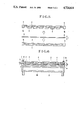
- FIGS. 1 to 5 are side sectional views for explaining the steps in a method of producing a semiconductor module according to an embodiment of the present invention.
- FIG. 6 is a side sectional view of a semiconductor module according to an embodiment of the present invention.
- FIGS. 1 to 5 are side sectional views sequentially showing the steps in the manufacture of the semiconductor module.
- a substrate frame 5 which has a substantially L-shaped section is fixed to the outer periphery of a substrate 4.
- a plurality of LSI semiconductor chips 3 are mounted on the lower surface of the substrate 4. The substrate frame 5 and the substrate 4 mounting the semiconductor chips 3 are thus capable of being integrally moved.
- a heat-conductive material 2 (in this embodiment, solder) which is melted by heating and solidified and contracted when cooled, is melted by heating and filled in a predetermined amount (to be described later) in a dish-like cooling chamber 1 having an outer periphery opposing a lower surface 5a of the substrate frame 5.
- the substrate frame 5 is mounted on and fixed to the cooling chamber 1, so that a lower surface 5a of the frame 5 abuts against an upper, outer peripheral surface 1a of chamber 1.
- the amount of molten solder 2 is predetermined, such that the surfaces of the chips 3 are sufficiently brought into contact with the surface of the molten solder 2 when the substrate frame 5 abuts against the cooling chamber 1.
- each of the chips 3 is subjected to a solder wet-prevention process. However, if each chip 3 is housed in a ceramic casing, the solder wet-prevention process need not be performed.
- Heating of the molten solder 2 is interrupted in the state shown in FIG. 3. Upon interruption of heating, the temperature of the molten solder 2 gradually decreases, and the molten solder is solidified while being contracted due to a decrease in temperature. Since each chip 3 is subjected to the solder wet-prevention process, a small gap 10 having a size h 1 is formed between the surface of the solidified solder 2 and the chips 3 due to contraction of the molten solder 2, as shown in FIG. 4.
- the substrate frame 5 is temporarily separated from the cooling chamber 1, thereby separating the chips 3 from the solder 2. Since the solder 2 has been solidified, it maintains the sectional shape shown in FIG. 4.
- the separated upper and lower portions are washed to remove foreign materials, e.g., flux.
- a spacer 6 having a thickness t is inserted between the lower surface 5a of the substrate frame 5 and the upper, outer peripheral surface 1a of the cooling chamber 1, and the resultant structure is then assembled.
- the thickness of the spacer 6 can be arbitrarily selected.
- the molten solder is charged in the cooling chamber 1.
- a predetermined amount of solder can be attached in advance to the cooling chamber 1, and the attached solder can be heated to be melted.
- the solder 2 is used.
- the present invention is not limited to solder, and other materials, i.e., heat-conductive materials which are contracted upon solidification, can also be used. Not only the materials which are melted by heating and solidified by cooling, but also such materials as EPO-TEK H 35-175 paste (produced by Epoxy Technology Inc.) which is in fluid state at normal temperature but solidified and contracted at a higher temperature than 180° C., can be used.
- FIG. 6 shows a side sectional view of an embodiment of a semiconductor module manufactured by the above-mentioned method.
- the same reference numerals in FIG. 6 denote the same parts as in FIGS. 1 to 5.
- Reference numeral 7 denotes an assembling screw extending through the substrate frame 5, the spacer 6, and the cooling chamber 1.
- Reference numeral 8 denotes a water-cooled jacket, which is fixed to the cooling chamber 1 and has a hollow portion 8a, through which water flows to perform a water cooling operation.
- This embodiment adopts a water-cooling structure, but can adopt an air-cooling structure if a fin is mounted on the cooling chamber 1.
- a spacer having a predetermined thickness t is inserted between a cooling chamber and a substrate holding member and the resultant structure is assembled. Therefore, if the thickness t of the spacer is appropriately selected, a small gap (h 1 +t) of an optimal size can be set between the chips and the heat-conductive material surface.
- the small gap can be reduced to be smaller than a total of dimensional errors and assembly errors of constituents, thus greatly reducing a heat resistance when compared with a conventional semiconductor module.
- a cooling capability can be noticeably improved.
Abstract
Description
Claims (5)
Applications Claiming Priority (2)
| Application Number | Priority Date | Filing Date | Title |
|---|---|---|---|
| JP18388985 | 1985-08-23 | ||
| JP60-183889 | 1985-08-23 |
Publications (1)
| Publication Number | Publication Date |
|---|---|
| US4724611A true US4724611A (en) | 1988-02-16 |
Family
ID=16143585
Family Applications (1)
| Application Number | Title | Priority Date | Filing Date |
|---|---|---|---|
| US06/898,428 Expired - Fee Related US4724611A (en) | 1985-08-23 | 1986-08-20 | Method for producing semiconductor module |
Country Status (3)
| Country | Link |
|---|---|
| US (1) | US4724611A (en) |
| JP (1) | JPS62122156A (en) |
| FR (1) | FR2586510B1 (en) |
Cited By (48)
| Publication number | Priority date | Publication date | Assignee | Title |
|---|---|---|---|---|
| US4945980A (en) * | 1988-09-09 | 1990-08-07 | Nec Corporation | Cooling unit |
| US4975766A (en) * | 1988-08-26 | 1990-12-04 | Nec Corporation | Structure for temperature detection in a package |
| US5014777A (en) * | 1988-09-20 | 1991-05-14 | Nec Corporation | Cooling structure |
| US5023695A (en) * | 1988-05-09 | 1991-06-11 | Nec Corporation | Flat cooling structure of integrated circuit |
| US5036384A (en) * | 1987-12-07 | 1991-07-30 | Nec Corporation | Cooling system for IC package |
| US5263245A (en) * | 1992-01-27 | 1993-11-23 | International Business Machines Corporation | Method of making an electronic package with enhanced heat sinking |
| US5360993A (en) * | 1991-10-21 | 1994-11-01 | Nec Corporation | Cooling unit capable of speedily cooling an integrated circuit chip |
| US5517753A (en) * | 1995-04-06 | 1996-05-21 | International Business Machines Corporation | Adjustable spacer for flat plate cooling applications |
| US5604978A (en) * | 1994-12-05 | 1997-02-25 | International Business Machines Corporation | Method for cooling of chips using a plurality of materials |
| US5978220A (en) * | 1996-10-23 | 1999-11-02 | Asea Brown Boveri Ag | Liquid cooling device for a high-power semiconductor module |
| US6049975A (en) * | 1992-09-16 | 2000-04-18 | Clayton; James E. | Method of forming a thin multichip module |
| US20040235222A1 (en) * | 2001-10-26 | 2004-11-25 | Staktek Group, L.P. | Integrated circuit stacking system and method |
| US20050139980A1 (en) * | 1992-12-11 | 2005-06-30 | Burns Carmen D. | High density integrated circuit module |
| US20050146011A1 (en) * | 2001-10-26 | 2005-07-07 | Staktek Group, L.P. | Pitch change and chip scale stacking system and method |
| US20050242423A1 (en) * | 2001-10-26 | 2005-11-03 | Staktek Group, L.P. | Stacked module systems and methods |
| US20060050498A1 (en) * | 2004-09-03 | 2006-03-09 | Staktek Group L.P. | Die module system and method |
| US20060049513A1 (en) * | 2004-09-03 | 2006-03-09 | Staktek Group L.P. | Thin module system and method with thermal management |
| US20060050492A1 (en) * | 2004-09-03 | 2006-03-09 | Staktek Group, L.P. | Thin module system and method |
| US20060050488A1 (en) * | 2004-09-03 | 2006-03-09 | Staktel Group, L.P. | High capacity thin module system and method |
| US20060050592A1 (en) * | 2004-09-03 | 2006-03-09 | Staktek Group L.P. | Compact module system and method |
| US20060049500A1 (en) * | 2004-09-03 | 2006-03-09 | Staktek Group L.P. | Thin module system and method |
| US20060050497A1 (en) * | 2004-09-03 | 2006-03-09 | Staktek Group L.P. | Buffered thin module system and method |
| US20060055024A1 (en) * | 2004-09-14 | 2006-03-16 | Staktek Group, L.P. | Adapted leaded integrated circuit module |
| US20060072297A1 (en) * | 2004-10-01 | 2006-04-06 | Staktek Group L.P. | Circuit Module Access System and Method |
| US7033861B1 (en) | 2005-05-18 | 2006-04-25 | Staktek Group L.P. | Stacked module systems and method |
| US20060092614A1 (en) * | 2001-10-26 | 2006-05-04 | Staktek Group, L.P. | Stacked module systems and methods |
| US20060118936A1 (en) * | 2004-12-03 | 2006-06-08 | Staktek Group L.P. | Circuit module component mounting system and method |
| US20060131716A1 (en) * | 2001-10-26 | 2006-06-22 | Cady James W | Stacking system and method |
| US20060175693A1 (en) * | 2005-02-04 | 2006-08-10 | Staktek Group, L.P. | Systems, methods, and apparatus for generating ball-out matrix configuration output for a flex circuit |
| US20060198238A1 (en) * | 2004-09-03 | 2006-09-07 | Staktek Group L.P. | Modified core for circuit module system and method |
| US20060203442A1 (en) * | 2004-09-03 | 2006-09-14 | Staktek Group, L.P. | Memory module system and method |
| US20060244114A1 (en) * | 2005-04-28 | 2006-11-02 | Staktek Group L.P. | Systems, methods, and apparatus for connecting a set of contacts on an integrated circuit to a flex circuit via a contact beam |
| US20060250780A1 (en) * | 2005-05-06 | 2006-11-09 | Staktek Group L.P. | System component interposer |
| US20060255446A1 (en) * | 2001-10-26 | 2006-11-16 | Staktek Group, L.P. | Stacked modules and method |
| US20060261449A1 (en) * | 2005-05-18 | 2006-11-23 | Staktek Group L.P. | Memory module system and method |
| US7193310B2 (en) | 2001-12-14 | 2007-03-20 | Stuktek Group L.P. | Stacking system and method |
| US20070176286A1 (en) * | 2006-02-02 | 2007-08-02 | Staktek Group L.P. | Composite core circuit module system and method |
| US20070201208A1 (en) * | 2006-02-27 | 2007-08-30 | Staktek Group L.P. | Active cooling methods and apparatus for modules |
| US20070258217A1 (en) * | 2004-09-03 | 2007-11-08 | Roper David L | Split Core Circuit Module |
| US20080067662A1 (en) * | 2001-10-26 | 2008-03-20 | Staktek Group L.P. | Modularized Die Stacking System and Method |
| US7443023B2 (en) | 2004-09-03 | 2008-10-28 | Entorian Technologies, Lp | High capacity thin module system |
| US7446410B2 (en) | 2004-09-03 | 2008-11-04 | Entorian Technologies, Lp | Circuit module with thermal casing systems |
| US7542297B2 (en) | 2004-09-03 | 2009-06-02 | Entorian Technologies, Lp | Optimized mounting area circuit module system and method |
| US7579687B2 (en) | 2004-09-03 | 2009-08-25 | Entorian Technologies, Lp | Circuit module turbulence enhancement systems and methods |
| US7606049B2 (en) | 2004-09-03 | 2009-10-20 | Entorian Technologies, Lp | Module thermal management system and method |
| US20090273069A1 (en) * | 2001-10-26 | 2009-11-05 | Cady James W | Low profile chip scale stacking system and method |
| US7616452B2 (en) | 2004-09-03 | 2009-11-10 | Entorian Technologies, Lp | Flex circuit constructions for high capacity circuit module systems and methods |
| US11240910B2 (en) * | 2020-04-27 | 2022-02-01 | Fu Tai Hua Industry (Shenzhen) Co., Ltd. | Heat dissipation structure and electronic device |
Families Citing this family (3)
| Publication number | Priority date | Publication date | Assignee | Title |
|---|---|---|---|---|
| DE69112389T2 (en) * | 1991-06-06 | 1996-03-21 | Ibm | Electronic packing module. |
| FR2766967A1 (en) * | 1997-07-31 | 1999-02-05 | Scps | Heat sink and electromagnetic protection device for pcb |
| DE102007041419B4 (en) * | 2007-08-31 | 2022-03-31 | Sew-Eurodrive Gmbh & Co Kg | Arrangement for cooling electrical components and converter and compact drive with it |
Citations (5)
| Publication number | Priority date | Publication date | Assignee | Title |
|---|---|---|---|---|
| US2999034A (en) * | 1960-10-21 | 1961-09-05 | Wenczler & Heidenhain | Method of manufacture of line plates, scales, and the like |
| JPS5586130A (en) * | 1978-12-25 | 1980-06-28 | Hitachi Ltd | Connection of semiconductor element |
| JPS5670655A (en) * | 1979-11-15 | 1981-06-12 | Matsushita Electric Ind Co Ltd | Manufacture of electronic circuit mounting device |
| US4439918A (en) * | 1979-03-12 | 1984-04-03 | Western Electric Co., Inc. | Methods of packaging an electronic device |
| US4467522A (en) * | 1981-04-11 | 1984-08-28 | Giuseppe Marchisi | Process for manufacturing plastic containers incorporating a heat disperser for integrated circuits |
-
1986
- 1986-08-20 US US06/898,428 patent/US4724611A/en not_active Expired - Fee Related
- 1986-08-21 FR FR8611948A patent/FR2586510B1/en not_active Expired - Fee Related
- 1986-08-22 JP JP61195539A patent/JPS62122156A/en active Granted
Patent Citations (5)
| Publication number | Priority date | Publication date | Assignee | Title |
|---|---|---|---|---|
| US2999034A (en) * | 1960-10-21 | 1961-09-05 | Wenczler & Heidenhain | Method of manufacture of line plates, scales, and the like |
| JPS5586130A (en) * | 1978-12-25 | 1980-06-28 | Hitachi Ltd | Connection of semiconductor element |
| US4439918A (en) * | 1979-03-12 | 1984-04-03 | Western Electric Co., Inc. | Methods of packaging an electronic device |
| JPS5670655A (en) * | 1979-11-15 | 1981-06-12 | Matsushita Electric Ind Co Ltd | Manufacture of electronic circuit mounting device |
| US4467522A (en) * | 1981-04-11 | 1984-08-28 | Giuseppe Marchisi | Process for manufacturing plastic containers incorporating a heat disperser for integrated circuits |
Non-Patent Citations (4)
| Title |
|---|
| Electrical Design and Analysis of the Air Cooled Module (ACM) in IBM System/4381, Nov. 1, 1983. * |
| Electrical Design and Analysis of the Air-Cooled Module (ACM) in IBM System/4381, Nov. 1, 1983. |
| New International and External Cooling Enhancements for the Air Cooled IBM 4381 Module, Nov. 1, 1983. * |
| New International and External Cooling Enhancements for the Air-Cooled IBM 4381 Module, Nov. 1, 1983. |
Cited By (80)
| Publication number | Priority date | Publication date | Assignee | Title |
|---|---|---|---|---|
| US5036384A (en) * | 1987-12-07 | 1991-07-30 | Nec Corporation | Cooling system for IC package |
| US5023695A (en) * | 1988-05-09 | 1991-06-11 | Nec Corporation | Flat cooling structure of integrated circuit |
| US4975766A (en) * | 1988-08-26 | 1990-12-04 | Nec Corporation | Structure for temperature detection in a package |
| US4945980A (en) * | 1988-09-09 | 1990-08-07 | Nec Corporation | Cooling unit |
| US5014777A (en) * | 1988-09-20 | 1991-05-14 | Nec Corporation | Cooling structure |
| US5360993A (en) * | 1991-10-21 | 1994-11-01 | Nec Corporation | Cooling unit capable of speedily cooling an integrated circuit chip |
| US5263245A (en) * | 1992-01-27 | 1993-11-23 | International Business Machines Corporation | Method of making an electronic package with enhanced heat sinking |
| US6049975A (en) * | 1992-09-16 | 2000-04-18 | Clayton; James E. | Method of forming a thin multichip module |
| US20050139980A1 (en) * | 1992-12-11 | 2005-06-30 | Burns Carmen D. | High density integrated circuit module |
| US5604978A (en) * | 1994-12-05 | 1997-02-25 | International Business Machines Corporation | Method for cooling of chips using a plurality of materials |
| US5724729A (en) * | 1994-12-05 | 1998-03-10 | International Business Machines Corporation | Method and apparatus for cooling of chips using a plurality of customized thermally conductive materials |
| US5517753A (en) * | 1995-04-06 | 1996-05-21 | International Business Machines Corporation | Adjustable spacer for flat plate cooling applications |
| US5719443A (en) * | 1995-04-06 | 1998-02-17 | International Business Machines Corporation | Adjustable spacer for flat plate cooling applications |
| US5978220A (en) * | 1996-10-23 | 1999-11-02 | Asea Brown Boveri Ag | Liquid cooling device for a high-power semiconductor module |
| US20060092614A1 (en) * | 2001-10-26 | 2006-05-04 | Staktek Group, L.P. | Stacked module systems and methods |
| US20090273069A1 (en) * | 2001-10-26 | 2009-11-05 | Cady James W | Low profile chip scale stacking system and method |
| US20050242423A1 (en) * | 2001-10-26 | 2005-11-03 | Staktek Group, L.P. | Stacked module systems and methods |
| US20050263872A1 (en) * | 2001-10-26 | 2005-12-01 | Cady James W | Flex-based circuit module |
| US7656678B2 (en) | 2001-10-26 | 2010-02-02 | Entorian Technologies, Lp | Stacked module systems |
| US20090298230A1 (en) * | 2001-10-26 | 2009-12-03 | Staktek Group, L.P. | Stacked Module Systems and Methods |
| US20040235222A1 (en) * | 2001-10-26 | 2004-11-25 | Staktek Group, L.P. | Integrated circuit stacking system and method |
| US20050146011A1 (en) * | 2001-10-26 | 2005-07-07 | Staktek Group, L.P. | Pitch change and chip scale stacking system and method |
| US7595550B2 (en) | 2001-10-26 | 2009-09-29 | Entorian Technologies, Lp | Flex-based circuit module |
| US20080067662A1 (en) * | 2001-10-26 | 2008-03-20 | Staktek Group L.P. | Modularized Die Stacking System and Method |
| US7202555B2 (en) | 2001-10-26 | 2007-04-10 | Staktek Group L.P. | Pitch change and chip scale stacking system and method |
| US20060131716A1 (en) * | 2001-10-26 | 2006-06-22 | Cady James W | Stacking system and method |
| US20060255446A1 (en) * | 2001-10-26 | 2006-11-16 | Staktek Group, L.P. | Stacked modules and method |
| US7193310B2 (en) | 2001-12-14 | 2007-03-20 | Stuktek Group L.P. | Stacking system and method |
| US20060050492A1 (en) * | 2004-09-03 | 2006-03-09 | Staktek Group, L.P. | Thin module system and method |
| US20060050488A1 (en) * | 2004-09-03 | 2006-03-09 | Staktel Group, L.P. | High capacity thin module system and method |
| US7768796B2 (en) | 2004-09-03 | 2010-08-03 | Entorian Technologies L.P. | Die module system |
| US7760513B2 (en) | 2004-09-03 | 2010-07-20 | Entorian Technologies Lp | Modified core for circuit module system and method |
| US7737549B2 (en) | 2004-09-03 | 2010-06-15 | Entorian Technologies Lp | Circuit module with thermal casing systems |
| US20060198238A1 (en) * | 2004-09-03 | 2006-09-07 | Staktek Group L.P. | Modified core for circuit module system and method |
| US20060203442A1 (en) * | 2004-09-03 | 2006-09-14 | Staktek Group, L.P. | Memory module system and method |
| US20060050498A1 (en) * | 2004-09-03 | 2006-03-09 | Staktek Group L.P. | Die module system and method |
| US20060049513A1 (en) * | 2004-09-03 | 2006-03-09 | Staktek Group L.P. | Thin module system and method with thermal management |
| US7626259B2 (en) | 2004-09-03 | 2009-12-01 | Entorian Technologies, Lp | Heat sink for a high capacity thin module system |
| US7616452B2 (en) | 2004-09-03 | 2009-11-10 | Entorian Technologies, Lp | Flex circuit constructions for high capacity circuit module systems and methods |
| US20060050497A1 (en) * | 2004-09-03 | 2006-03-09 | Staktek Group L.P. | Buffered thin module system and method |
| US20060049500A1 (en) * | 2004-09-03 | 2006-03-09 | Staktek Group L.P. | Thin module system and method |
| US20060050496A1 (en) * | 2004-09-03 | 2006-03-09 | Staktek Group L.P. | Thin module system and method |
| US7606040B2 (en) | 2004-09-03 | 2009-10-20 | Entorian Technologies, Lp | Memory module system and method |
| US7606042B2 (en) | 2004-09-03 | 2009-10-20 | Entorian Technologies, Lp | High capacity thin module system and method |
| US7606049B2 (en) | 2004-09-03 | 2009-10-20 | Entorian Technologies, Lp | Module thermal management system and method |
| US7606050B2 (en) | 2004-09-03 | 2009-10-20 | Entorian Technologies, Lp | Compact module system and method |
| US20070258217A1 (en) * | 2004-09-03 | 2007-11-08 | Roper David L | Split Core Circuit Module |
| US7324352B2 (en) | 2004-09-03 | 2008-01-29 | Staktek Group L.P. | High capacity thin module system and method |
| US20080030966A1 (en) * | 2004-09-03 | 2008-02-07 | Staktek Group L.P. | High Capacity Thin Module System and Method |
| US20060050592A1 (en) * | 2004-09-03 | 2006-03-09 | Staktek Group L.P. | Compact module system and method |
| US7423885B2 (en) | 2004-09-03 | 2008-09-09 | Entorian Technologies, Lp | Die module system |
| US7443023B2 (en) | 2004-09-03 | 2008-10-28 | Entorian Technologies, Lp | High capacity thin module system |
| US7446410B2 (en) | 2004-09-03 | 2008-11-04 | Entorian Technologies, Lp | Circuit module with thermal casing systems |
| US20080278901A9 (en) * | 2004-09-03 | 2008-11-13 | Staktek Group, L.P. | Memory module system and method |
| US20080278924A1 (en) * | 2004-09-03 | 2008-11-13 | Entorian Technologies, L.P. (Formerly Staktek Group L.P.) | Die module system |
| US7459784B2 (en) | 2004-09-03 | 2008-12-02 | Entorian Technologies, Lp | High capacity thin module system |
| US7468893B2 (en) | 2004-09-03 | 2008-12-23 | Entorian Technologies, Lp | Thin module system and method |
| US7480152B2 (en) | 2004-09-03 | 2009-01-20 | Entorian Technologies, Lp | Thin module system and method |
| US20090052124A1 (en) * | 2004-09-03 | 2009-02-26 | Entorian Technologies, L.P. (Formerly Staktek Group, L.P) | Circuit Module with Thermal Casing Systems |
| US7602613B2 (en) | 2004-09-03 | 2009-10-13 | Entorian Technologies, Lp | Thin module system and method |
| US7511968B2 (en) | 2004-09-03 | 2009-03-31 | Entorian Technologies, Lp | Buffered thin module system and method |
| US7522421B2 (en) | 2004-09-03 | 2009-04-21 | Entorian Technologies, Lp | Split core circuit module |
| US7522425B2 (en) | 2004-09-03 | 2009-04-21 | Entorian Technologies, Lp | High capacity thin module system and method |
| US7542297B2 (en) | 2004-09-03 | 2009-06-02 | Entorian Technologies, Lp | Optimized mounting area circuit module system and method |
| US7579687B2 (en) | 2004-09-03 | 2009-08-25 | Entorian Technologies, Lp | Circuit module turbulence enhancement systems and methods |
| US20060055024A1 (en) * | 2004-09-14 | 2006-03-16 | Staktek Group, L.P. | Adapted leaded integrated circuit module |
| US20060072297A1 (en) * | 2004-10-01 | 2006-04-06 | Staktek Group L.P. | Circuit Module Access System and Method |
| US20060118936A1 (en) * | 2004-12-03 | 2006-06-08 | Staktek Group L.P. | Circuit module component mounting system and method |
| US20060175693A1 (en) * | 2005-02-04 | 2006-08-10 | Staktek Group, L.P. | Systems, methods, and apparatus for generating ball-out matrix configuration output for a flex circuit |
| US20060244114A1 (en) * | 2005-04-28 | 2006-11-02 | Staktek Group L.P. | Systems, methods, and apparatus for connecting a set of contacts on an integrated circuit to a flex circuit via a contact beam |
| US20060250780A1 (en) * | 2005-05-06 | 2006-11-09 | Staktek Group L.P. | System component interposer |
| US20070126125A1 (en) * | 2005-05-18 | 2007-06-07 | Staktek Group L.P. | Memory Module System and Method |
| US20060261449A1 (en) * | 2005-05-18 | 2006-11-23 | Staktek Group L.P. | Memory module system and method |
| US7033861B1 (en) | 2005-05-18 | 2006-04-25 | Staktek Group L.P. | Stacked module systems and method |
| US20070126124A1 (en) * | 2005-05-18 | 2007-06-07 | Staktek Group L.P. | Memory Module System and Method |
| US20070176286A1 (en) * | 2006-02-02 | 2007-08-02 | Staktek Group L.P. | Composite core circuit module system and method |
| US7511969B2 (en) | 2006-02-02 | 2009-03-31 | Entorian Technologies, Lp | Composite core circuit module system and method |
| US20070201208A1 (en) * | 2006-02-27 | 2007-08-30 | Staktek Group L.P. | Active cooling methods and apparatus for modules |
| US7289327B2 (en) | 2006-02-27 | 2007-10-30 | Stakick Group L.P. | Active cooling methods and apparatus for modules |
| US11240910B2 (en) * | 2020-04-27 | 2022-02-01 | Fu Tai Hua Industry (Shenzhen) Co., Ltd. | Heat dissipation structure and electronic device |
Also Published As
| Publication number | Publication date |
|---|---|
| JPH0573263B2 (en) | 1993-10-14 |
| FR2586510A1 (en) | 1987-02-27 |
| FR2586510B1 (en) | 1990-06-15 |
| JPS62122156A (en) | 1987-06-03 |
Similar Documents
| Publication | Publication Date | Title |
|---|---|---|
| US4724611A (en) | Method for producing semiconductor module | |
| US5821161A (en) | Cast metal seal for semiconductor substrates and process thereof | |
| US5982038A (en) | Cast metal seal for semiconductor substrates | |
| US4654966A (en) | Method of making a dimensionally stable semiconductor device | |
| US5219794A (en) | Semiconductor integrated circuit device and method of fabricating same | |
| EP0104204B1 (en) | Cast solder leads for leadless semiconductor circuits | |
| KR940001283B1 (en) | Seramic pack type semiconductor device and assembling method of the same | |
| EP0875932B1 (en) | Manufacturing methods for a semiconductor | |
| US5639696A (en) | Microelectronic integrated circuit mounted on circuit board with solder column grid array interconnection, and method of fabricating the solder column grid array | |
| US6162659A (en) | Method for manufacturing a package structure having a heat spreader for integrated circuit chips | |
| JPS6054785B2 (en) | Method of manufacturing integrated circuit assembly | |
| JPH07147466A (en) | Electronic component unit and manufacture thereof | |
| US6472305B1 (en) | Method of manufacturing bonded structure of film substrate and semiconductor chip | |
| US5894984A (en) | Structure of electronic parts and method of soldering electronic parts to substrate | |
| EP0482812B1 (en) | Method for manufacturing semiconductor-mounting heat-radiative substrates and semiconductor package using the same | |
| US6773966B2 (en) | Method of manufacturing semiconductor device | |
| JP5343334B2 (en) | Welded structure and manufacturing method thereof | |
| JP3113400B2 (en) | Electronic circuit device | |
| US20030134452A1 (en) | Method for manufacturing semiconductor device packages | |
| JPS5987843A (en) | Manufacture of semiconductor cooling device | |
| JP2003258172A (en) | Method for assembling multi-chip module | |
| JPS60175433A (en) | Manufacture of resin-sealed semiconductor device and lead frame | |
| JPH098185A (en) | Package with electronic-component cooling structure and its manufacture | |
| JPH09148636A (en) | Manufacture of thermoelectric device | |
| JPH0426550B2 (en) |
Legal Events
| Date | Code | Title | Description |
|---|---|---|---|
| AS | Assignment |
Owner name: NEC CORPORATION, 33-1, SHIBA 5-CHOME, MINATO-KU, T Free format text: ASSIGNMENT OF ASSIGNORS INTEREST.;ASSIGNOR:HAGIHARA, TAKASHI;REEL/FRAME:004593/0718 Effective date: 19860808 Owner name: NEC CORPORATION, A CORP. OF JAPAN,JAPAN Free format text: ASSIGNMENT OF ASSIGNORS INTEREST;ASSIGNOR:HAGIHARA, TAKASHI;REEL/FRAME:004593/0718 Effective date: 19860808 |
|
| FEPP | Fee payment procedure |
Free format text: PAYOR NUMBER ASSIGNED (ORIGINAL EVENT CODE: ASPN); ENTITY STATUS OF PATENT OWNER: LARGE ENTITY |
|
| FPAY | Fee payment |
Year of fee payment: 4 |
|
| FPAY | Fee payment |
Year of fee payment: 8 |
|
| FEPP | Fee payment procedure |
Free format text: PAYOR NUMBER ASSIGNED (ORIGINAL EVENT CODE: ASPN); ENTITY STATUS OF PATENT OWNER: LARGE ENTITY Free format text: PAYER NUMBER DE-ASSIGNED (ORIGINAL EVENT CODE: RMPN); ENTITY STATUS OF PATENT OWNER: LARGE ENTITY |
|
| REMI | Maintenance fee reminder mailed | ||
| LAPS | Lapse for failure to pay maintenance fees | ||
| FP | Lapsed due to failure to pay maintenance fee |
Effective date: 20000216 |
|
| STCH | Information on status: patent discontinuation |
Free format text: PATENT EXPIRED DUE TO NONPAYMENT OF MAINTENANCE FEES UNDER 37 CFR 1.362 |