US4562538A - Microprocessor having decision pointer to process restore position - Google Patents
Microprocessor having decision pointer to process restore position Download PDFInfo
- Publication number
- US4562538A US4562538A US06/494,776 US49477683A US4562538A US 4562538 A US4562538 A US 4562538A US 49477683 A US49477683 A US 49477683A US 4562538 A US4562538 A US 4562538A
- Authority
- US
- United States
- Prior art keywords
- bit
- point
- interruption
- block
- beginning
- Prior art date
- Legal status (The legal status is an assumption and is not a legal conclusion. Google has not performed a legal analysis and makes no representation as to the accuracy of the status listed.)
- Expired - Lifetime
Links
Images


Classifications
-
- G—PHYSICS
- G06—COMPUTING; CALCULATING OR COUNTING
- G06F—ELECTRIC DIGITAL DATA PROCESSING
- G06F9/00—Arrangements for program control, e.g. control units
- G06F9/06—Arrangements for program control, e.g. control units using stored programs, i.e. using an internal store of processing equipment to receive or retain programs
- G06F9/46—Multiprogramming arrangements
- G06F9/461—Saving or restoring of program or task context
- G06F9/463—Program control block organisation
Definitions
- This invention is directed at a data processing system and, more particularly, at a system for carrying out context (or process) switch operations in a multiprogramming environment.
- program defines a stream of both instructions and data that a user can request an operating system to transfer, link, and execute.
- An "executable” program in memory is called an "image”.
- image An "executable” program in memory
- process The (hardware) context in which an image is executed is called a “process” and the term “process” thus characterizes the complete unit of execution in the computer system.
- a context (or process) switch operation can be understood to occur in a multiprogramming environment where several processes (individual streams of code) are ready for execution at any one time.
- the term "process switch operation” thus refers to the procedure for reassigning the processor from a currently running process to a successor process.
- a processor In order to achieve a high performance system, a processor has to be structured to enable the operating system to switch execution rapidly between individual processes. Since a process is a stream of instructions and data defined by a hardware context, each process has a unique identification in the computer system, the stream of code being executed at any instant being determined by its hardware context.
- the term "hardware context" refers to the information loaded in the processor's registers that identifies where the stream of instructions and data are located, which instruction to execute next, and what the processor status is during execution.
- the computer's operating system switches between processes by requesting the processor to save one process hardware context and load another via a specific set of instructions.
- a microprocessor typically includes one or more programmed logic arrays (PLAs) each with word lines along which a pattern of transistors are defined in a manner determinative of output codes operative to control various other elements of the microprocessor.
- the pattern of transistors along each word line is called "microcode", the totality of microcode lines defined by a PLA being referred to as a "microprogram”.
- Each word line specifically, defines a particular set of output bits representative of a line of microcode. Sequences of microcode instructions are generated at the output register of the PLA and applied to various registers, inter alia, to control data flow and processing on the chip, often responsive to a single instruction at the input to the PLA.
- An input instruction to a PLA is referred to as an "opcode", a sequence of such instructions being referred to as “macrocode”. It is common during operation for instructions to be introduced to the chip from a memory which is external to the chip. Such instructions often are latched in an on-chip instruction register for processing under the control of the PLA.
- a “process switch operation”, in this context, is controlled by a sequence of microcode instructions generated at the output register of a PLA.
- the processor When a process switch operation occurs in a prior art system, the processor operates in two phases: the first phase is to save (store) the current state of the interrupted process for resumption at a later time. The second phase is to set up (restore) the new state for the successor process. At the conclusion of the successor process, the processor operates to re-establish the state of the previous (or some other) process.
- SP stack pointer
- PC program counter
- PSW process status word
- the invention is based on the realization that an "initializing" or "I" bit may be stored to an advantage in the PSW to indicate whether an interrupted process is to be restored, at a later time, at the beginning of the process or at the point of interruption.
- This I bit is employed in conjunction with a process control block (PCB) in memory.
- the PCB contains initial process context information (PSW, PC and SP) in the first 12 bytes or in the second 12 bytes. If the I bit is a binary one, the PCB pointer is set to the first address in the PCB and the contents of the PSW, PC and SP registers of the interrupted process are stored in the second 12-byte addresses. If the I bit is a binary zero, the pointer points to the 13th address in the PCB when a process switch occurs.
- a process requires initial values for the SP, the PC and the PSW so the process can be started in the correct state, as indicated in steps 3 and 4 of Table I.
- a process once started, may itself be interrupted by another.
- the state of the first process somewhere in the middle of its execution, is saved in memory, as indicated in steps 1 and 2 of Table I. If the first process must, at some later time, be started with its initial values, the memory used for storing the intermediate state must be different from the memory where the initial state is stored.
- a processor using the principles of the invention includes means responsive to a request for a process switch to a process that will use different memory for steps 3 and 4 than for steps 1 and 2.
- each process includes means for controlling the adjustment of the area used for saving the process state. Significant improvement in the (average) time required to perform a process switch operation is achieved as a result.
- an I bit is added to the PSW register and additional hardware is included in the datapath portion of the microprocessor for testing the value of that bit.
- the additional hardware is operative in cooperation with a microprogam stored in on-chip ROM (read only memory) to interconnect means responsive to a process switch command for instructing a PLA to execute the desired operation.
- the process switch operation is accomplished by a second microprogram in the absence of additional hardware.
- the microprogram in this instance also, is stored in ROM and is responsive, for example, to macrocode via an instruction register (and PLAs) for executing an operation.
- the PCBs are of lengths N and N+M where M is allocated to accommodate initialization information for those processes which are restored to process at the beginning position.
- the "I" bit determines whether or not the PCBP should be adjusted to point to a different area of memory to provide space for saving the PC, the PSW and the SP on a process switch. Specifically, during a process switch operation, the I bit in the PSW is saved, and possibly modified, in a manner to control the adjustment of the PCBP.
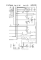
- FIGS. 1, 2 and 3 are block diagrams of an illustrative semiconductor microprocessor chip
- FIGS. 4 and 5 are schematic representations of the organization of the microprocessor of FIGS. 2 and 3;
- FIGS. 6 and 7 are circuit schematics of portions of the microprocessor of FIG. 1;
- FIG. 8 is a flow diagram of the operation of a portion of the microprocessor of FIGS. 1, 2 and 3;
- FIGS. 9-16 are block diagrams of memory sections and registers in the microprocessor of FIG. 1 showing data control therein during operation;
- FIG. 17 is a block diagram of the relationship between FIGS. 1, 2 and 3.
- FIGS. 1, 2 and 3 show a block diagram of a semiconductor microprocessor chip 10.
- the chip has defined in it a plurality of programmable logic arrays (PLAs) represented by blocks 12, 13, 14, 15 and 16.
- PLAs programmable logic arrays
- the various PLAs are interconnected into a control hierarchy in accordance with the teachings of U.S. Pat. No. 4,399,516.
- the blocks are labeled according to function as MAIN control, ACCESS control, ADDRESS control, DISTRIBUTION control and ARITHMETIC logic unit (ALU) control, respectively.
- the various PLAs are interconnected to interact with one another to control the operation of the datapath portion of the chip as is described more fully hereinafter.
- the datapath portion of the chip comprises the elements which carry out operations on data from memory.
- the datapath typically includes user registers, temporary registers, an arithmetic logic unit (ALU), address arithmetic unit (AAU), counters, etc.
- ALU arithmetic logic unit
- AAU address arithmetic unit
- the datapath portion of chip 10 includes specifically, an ALU 30 along with two temporary registers 31 and 32, TA and TB, as shown in FIG. 3.
- the outputs of the registers are connected to inputs to the ALU.
- the ALU carries out operations on data applied by the registers to the ALU according to the microcode applied to the ALU from the ALU control PLA over lines represented by symbolic line 33.
- the output of the ALU is applied to temporary register 35 to be applied to the "C-BUS" by means of tri-state buffer 37.
- the data in the temporary registers originates from selected ones of user registers 40 or from memory locations.
- a PSW (process status word) register 42 is connected to the C-BUS via a tri-state buffer 43.
- the PSW register is a special purpose register that a program uses to check its status and to control synchronous error conditions.
- the process status word contains two sets of bit fields, the condition codes and the trap enable flags similar to those described in the VAX 11-780 Hardware Handbook, 1978 edition by Digital Equipment Corporation on page 43, et seq.
- a program counter (PC) 45 of FIG. 2 is connected between the A-BUS at its input and the output of the access control PLA 13.
- the output of the program counter is connected to the R-BUS via tri-state buffer 48.
- the output of PLA 13 also is connected to the gate input of buffer 48.
- a program counter master latch 49 is connected between the output of the program counter and the A-BUS.
- the output of latch 49 is connected to the input of a slave latch 50.
- Slave latch 50 is connected to the A-BUS via a tri-state buffer 51.
- the gate input to buffer 51 is connected to the output of Access Control PLA 13.
- Program counter 45 contains the address of the next instruction to be executed as described on page 41 of the above-mentioned VAX-11 handbook and permits a programmer to write position independent code as is well understood in the art.
- An Address Arithmetic Unit 60 and associated address latch 61 are connected serially between the output of Address Control PLA 14 and the A-BUS via tri-state buffer 62.
- the tri-state buffer gate input is connected via AND circuit 65 to the output of PLA 13.
- Another input to circuit 65 is connected to the output of distribution control PLA 15.
- Outputs from Q latch and R latch 66 and 67, respectively, are connected to inputs to ALU 60.
- Queue 70 applies its output to latch 66 via tri-state buffer 71 and, via the I-BUS, to instruction registers (latches) at the inputs to MAIN, ADDRESS, and DISTRIBUTION PLAs 12, 14 and 15.
- Each of the outputs represents an opcode from the macroprogram stream.
- Latch 67 accepts data from a selected user register.
- the AAU forms the address of the operand from the two inputs.
- the microprocessor is operative to execute operations in ALU 30 under control of ALU control PLA 16 on data determined and organized by PLAs 14 and 15.
- Distribution PLA 15 controls the A- and C-BUS multiplexer 100 by controlling the data path from memory and the address arithmetic unit controls the loading of data into temporary registers 31 and 32 via output buffer 62 if the AAU result represents data (not an address).
- PLA 16 controls the ALU operation.
- the access control PLA 13 performs access of memory 72 using addresses formed by AAU 60 under control of PLA 14 under the control of MAIN PLA 12 as described in the above-mentioned patent application of Blahut et al.
- Example unit The foregoing portion of the microprocessor is commonly referred to as the "Execute" unit and is shown in more simplified block diagram form in FIG. 4.
- Data from memory are stored selectively in user register array 40 via the A-BUS and A- and C-BUS multiplexer 100.
- Data are moved to the temporary registers 31 and 32 of FIG. 3 shown collectively as 101 in FIG. 4 via a barrel switch 102 described in U.S. Pat. No. 4,396,994.
- PLAs 13 and 14 of FIG. 5 control the movement of instructions (opcode) and data from memory. Data is moved to user registers or other destinations on chip; opcodes go to the queue 70. Program counter 49 increments to point to the next memory address.
- AAU 60 which contains an adder, controls more complex address changes as is well understood.
- Memory 72 stores a number of processes in association with process control blocks.
- the processes are designated P 1 , P 2 . . . P n and the associated process control blocks are designated PCB1, PCB2 . . . PCBM.
- the process control block contains all of the switchable process information collected into compact form for ease of movement to and from the internal (user visible) registers as described in the above-noted VAX-11 780 Hardware Handbook starting on page 59.
- ROM Read only memory
- PLA 12 When a process switch command is moved from memory to queue 70 as part of a program, command signals are applied to MAIN control PLA 12 which recognizes the command as a process switch instruction.
- Read only memory (ROM) 103 indicates a set of process switch instructions to be applied to PLA 12 for organizing the operation of the processor for carrying out the process switch operation. Those instructions are in addresses in ROM and are accessed by PLA 12 in response to the signals applied to PLA 12.
- the instructions are included in a computer program along with comments identified as Appendix A herein.
- the program is a fragment written in a form of assembly language similar to that used with the above-mentioned VAX computer. Sufficient comments are provided to enable one skilled in assembly languages to understand the fragment.
- a process control block pointer is located in one of the user registers 40.
- the PCBP is changed from that of the current process to that of the new process.
- the stack pointer SP--located in one of the user registers of array 40
- the program counter PC
- the process status word PSW
- main control PLA 12 performs operations which copy the data in the PC, the SP and the PSW registers into the PCB (in memory) of the currently running process.
- Whether or not the data in the general registers is to be copied into the PCB of the currently running process is determined by the R bit in the PSW. Specifically, during a process switch operation, the R bit in the PSW is used, and possibly modified, in a manner to control the copying of the contents of the general purpose registers into the PCB. The function of the R bit is described in detail in U.S. Pat. No. 4,484,274. The determination as to whether the interrupted process later restarts at the point of interruption or at the beginning of the process is made in response to the I bit.
- the fetch unit operates in the traditional mode to fetch data and instructions from memory 72. That is, when a program which is being executed currently calls for instructions or data or both from memory, PLAs 12, 13 and 14 operate to access the corresponding addresses in memory and to apply the contents of the address (or sequence of addresses) to the address and data BUS 90 for storage in queue 70. Data are also moved along the A-BUS and via the multiplexer 100 to the C-BUS for storage in user register 40 or in temporary registers 31 and 32. As the instructions are executed, program counter 49 is incremented in the usual fashion under the control of address control PLA 14. When the program calls for a subroutine stored in ROM 103, address control PLA 14 responds to clear the queue and to move the contents of the corresponding addresses in ROM to the queue for execution.
- the memory block, say P 2 of FIG. 1 representing the new process is accompanied by a process control block, say PCB2 of FIG. 1.
- the process control block includes data for reorganizing the hardware for providing the necessary context for the new process--all the data needed to load the processor's programmable registers when a process switch operation is called for.
- PCBP process control block base register
- the I bit determines whether the new process is initiated at its beginning or at a point at which it was previously interrupted.
- FIGS. 6 and 7 show hardware added to a microprocessor (in one particular embodiment) for determining the value of the I bit in the process status word (PSW).
- the hardware is operative with the program of Appendix A.
- FIG. 6 shows the PSW register 42 including a latch 200.
- Data from a selected process control block (i.e., PCB2) in memory 72 is applied in parallel to the data input (D) of the latches of the register via the C-BUS as indicated in the Figure.
- Appropriate timing is applied to the clock input (C) of the latches of the register by the distribution control PLA 15.
- An OR circuit 201 is provided with inputs connected to the C-BUS and to outputs from PLA 15.
- the output (Q) 202 of latch 200 is connected to the C-BUS and to an input to PLA 15.
- the former connection is for storing the bit, along with others of the PSW, in the current PCB reflecting the instantaneous status of the current process.
- the latter connection is for the purpose of reading the I bit and for making a decision.
- the organization and operation of the illustrative embodiments herein are consistent with the description in the above-noted VAX-11 780 Hardware Handbook with the exception that an I bit is added and that a decision is made on the basis of that bit as to the point at which a restored process is initiated when a process switch operation is called for.
- FIG. 7 shows the logic circuitry associated with using the I bit (latch 200).
- the I-BUS is connected to the data inputs of 8-bit latch 250.
- the c inputs to the latch are connected to the ⁇ 1 output of the clock (not shown).
- the output (Q) of latch 250 is connected to an input of decoder 251.
- the output of ROM 103 of FIG. 2 is connected to a second input of decoder 251.
- the output of decoder 251 is connected to the data (D) inputs to 8-bit latch 252.
- the output of AND circuit 253 is connected to the clock inputs of latch 252.
- the inputs to AND circuit 253 are connected to the ⁇ 3 clock output of the clock circuit and to the output of MAIN PLA 12 for receiving signal SIG-1.
- Latch 257 is a tristatable clocked buffer having a floating output except during phase ⁇ 1 .
- the output of latch 257 is connected to one input of AND circuit 260.
- the ⁇ 3 output of the clock circuit is connected to a second output of circuit 260.
- the output of circuit 260 is connected to the input of buffer 261.
- the output of buffer 261 is connected to the clock input (c) of latch 200.
- Line 263 connects the C-BUS (FIG. 3) to the data input of latch 200.
- the output (202) of latch 200 is connected to the C-BUS (FIG. 1) via bus drivers and to PLA 15.
- the data on the I-BUS is latched onto latch 250 by clock signal ⁇ 1 .
- the content of latch 250 is decoded along with signal MMACN, a ROM-ON signal which indicates that code is being executed out of ROM 103. If the content of latch 250 and signal MMACN indicate that an I bit reference is desired, the signal MIBR (the I bit reference signal) is asserted, as shown, at the output of decoder 251.
- Signal MIBR is latched by signal SIG 1 from MAIN PLA 12 enabled by clock signal ⁇ 3 .
- Signal MCBR indicates that a data value is to be written from the C-BUS into a register.
- the resulting bit of the signal on line 255 is combined with signal MCBR from distribution PLA (15).
- the resulting signal is delayed to phase ⁇ 1 at latch 257.
- phase ⁇ 3 if the output of latch 257 is high, the corresponding data bit on the C-BUS is latched into the I bit latch 200 of PSW register 42.
- FIG. 8 shows a flow chart of the sequence of operations when an interrupt is invoked in the ordinary sequence of events.
- An interrupt causes one (current) process to be suspended and a new process to be initiated on the processor.
- Block B1 in the Figure represents the initialization of the sequence. This includes fetching an interrupt identifier from an external device and fetching a PCBP for the interrupt process.
- Block B3 in the Figure represents the storing of the PCBP of the current process on the interrupt stack.
- the register array 40 of FIG. 3 includes an interrupt stack pointer which supplies the memory location for storing the PCBP.
- Block B4 represents the action where the PC, SP and PSW registers are stored into the PCB (Process Control Block) of the current process, in memory pointed to by the PCBP.
- the PCBP is then set to the PCBP of the interrupt process, and the PC, SP and PSW registers are loaded from the PCB of the interrupt process.
- Block B5 represents the evaluation of the I bit of the new PSW. If the bit is a binary 1, the PCBP register is incremented by 12, as indicated in Block B6. The PCBP will then point past the memory which contained the initial values of the PC, SP and PSW registers for the interrupt process. In addition, the I bit of the PSW will be set to 0. If the I bit is a binary 0, no action is taken.
- Block B7 represents the completion of the interrupt sequence process switch, and the initiation of the process execution.
- Block B2 represents the initiation of this sequence, which includes fetching a PCBP for the new process. After Block B2 the sequence continues with Block B3, and proceeds in exactly the same manner as the interrupt sequence described above.
- the I bit is particularly useful for processes initiated by an interrupt sequence, since it is likely that an interrupt process will be executed many times, once for each time a device causes an interrupt, and each time the process generated should execute in the same way. If the I bit of the interrupt process is set, the initial values of the control registers will be preserved for the next invocation of the process, even if the current process is itself interrupted.
- FIGS. 9-16 depict the registers PSW and PCBP along with the contents of memory representing the Process Control Block (PCB) of a process.
- the PCB provides memory space to save the processor state when a process is interrupted and the I bit function assures that the initial PCB is not corrupted by the interrupt. If the function was not provided, another means of initiating a process would be necessary, and the adjustment of the PCB would have to take place separately.
- FIGS. 9 and 10 show the initial state of the pertinent section of memory and the two registers.
- FIG. 9 designates the pertinent section of memory as the "PCB" in which the first three control registers are stored, as well as space for other data.
- the pertinent section of memory in FIG. 9 also includes the image of the PSW register with the I bit set to 1. Note that the section of memory shown in FIG. 9 is labeled "PCB of process to be executed", which may, for example, correspond to PCB1 of memory 72 of FIG. 2.
- FIG. 10 shows the registers PSW and PCBP in their initial state.
- the I bit is initially in an unknown state, as is the PCBP.
- FIGS. 11 and 12 represent the state of the microprocessor after the new process has been initiated, either after response to an interrupt or by executing a "call process” (CALLPS) instruction.
- FIG. 11 represents the PCB of the process, as in FIG. 9, and
- FIG. 12 represents the registers PSW and PCBP. Note that the I bit of he PSW has been set to 0, while the I bit of the PCB has remained at 1. Because of this, the I bit initialization function will not be reexecuted for the process if it is interrupted at a later time by another process. The I bit of the "space reserved for the PSW" is unknown; it will be set to that of the PSW if the process is interrupted. Also, the PCBP points to the "space reserved for the PSW", not the "old PSW.”
- FIGS. 13 and 14 The initial state in the instance where the I bit of the new process equals 0 is shown in FIGS. 13 and 14.
- the individual Figures are designated as were their counterparts in FIGS. 9 and 10.
- FIGS. 15 and 16 represent the state of the microprocessor after the new process has been initiated when the initial state of the I bit of the PSW in the PCB was 0. Note that the I bit of both the PSW and the memory image of the PSW in the PCB is 0. Also, the PCBP points to "initial PSW.”
- FIG. 8 and FIGS. 9-16 The operation indicated in FIG. 8 and FIGS. 9-16 is implemented with special circuitry as shown in FIGS. 6 and 7 and with microcode stored in ROM.
- This special circuitry enables testing for the I bit to be more efficient than it would be in its absence.
- the microcode above is modified to test the I bit with ordinary microinstructions.
- the microprogram for this embodiment is shown with comments in Appendix B.
- the lines of code indicated by the notation #**# are changed from the program of Appendix A to enable the processor to operate without the special circuitry.
- a third embodiment would not use an I bit at all, but instead would perform the operation with a regular instruction executed as the first instruction of the process.
- This instruction would add 12 (the number of bytes in the three words of memory required to store the PSW, the PC and the SP) to the PCBP.
- the microprogram for this embodiment is shown in Appendix C.
- the program of Appendix C is a modification of that shown in Appendix A where lines of the former are deleted.
- each process with the additional instruction constitutes a control means for controllably restoring an interrupted process at the beginning or at the point of interruption when a process switch operation occurs. ##SPC1##
Abstract
Description
              TABLE I
______________________________________
1.  save SP, PC, and PSW registers of current
                             STORE
    process
2.  save general purpose registers of current
    process
3.  set up SP, PC and PSW registers for new
                             RESTORE
    process
4.  set up general purpose registers for new
    process
______________________________________
Claims (4)
Priority Applications (1)
| Application Number | Priority Date | Filing Date | Title |
|---|---|---|---|
| US06/494,776 US4562538A (en) | 1983-05-16 | 1983-05-16 | Microprocessor having decision pointer to process restore position |
Applications Claiming Priority (1)
| Application Number | Priority Date | Filing Date | Title |
|---|---|---|---|
| US06/494,776 US4562538A (en) | 1983-05-16 | 1983-05-16 | Microprocessor having decision pointer to process restore position |
Publications (1)
| Publication Number | Publication Date |
|---|---|
| US4562538A true US4562538A (en) | 1985-12-31 |
Family
ID=23965915
Family Applications (1)
| Application Number | Title | Priority Date | Filing Date |
|---|---|---|---|
| US06/494,776 Expired - Lifetime US4562538A (en) | 1983-05-16 | 1983-05-16 | Microprocessor having decision pointer to process restore position |
Country Status (1)
| Country | Link |
|---|---|
| US (1) | US4562538A (en) |
Cited By (21)
| Publication number | Priority date | Publication date | Assignee | Title |
|---|---|---|---|---|
| US4876640A (en) * | 1986-02-07 | 1989-10-24 | Advanced Micro Devices, Inc. | Logic controller having programmable logic "and" array using a programmable gray-code counter |
| US4972312A (en) * | 1985-11-04 | 1990-11-20 | U.S. Philips Corporation | Multiprocess computer and method for operating same having context switching in response to a peripheral interrupt |
| US5043879A (en) * | 1989-01-12 | 1991-08-27 | International Business Machines Corporation | PLA microcode controller |
| US5168566A (en) * | 1983-11-25 | 1992-12-01 | Sharp Kabushiki Kaisha | Multi-task control device for central processor task execution control provided as a peripheral device and capable of prioritizing and timesharing the tasks |
| US5226122A (en) * | 1987-08-21 | 1993-07-06 | Compaq Computer Corp. | Programmable logic system for filtering commands to a microprocessor |
| US5280615A (en) * | 1990-03-23 | 1994-01-18 | Unisys Corporation | Out of order job processing method and apparatus |
| US5363503A (en) * | 1992-01-22 | 1994-11-08 | Unisys Corporation | Fault tolerant computer system with provision for handling external events |
| US5428779A (en) * | 1992-11-09 | 1995-06-27 | Seiko Epson Corporation | System and method for supporting context switching within a multiprocessor system having functional blocks that generate state programs with coded register load instructions |
| US5450349A (en) * | 1992-10-27 | 1995-09-12 | Digital Equipment Corporation | Computer system performance evaluation system and method |
| US5490272A (en) * | 1994-01-28 | 1996-02-06 | International Business Machines Corporation | Method and apparatus for creating multithreaded time slices in a multitasking operating system |
| US5526521A (en) * | 1993-02-24 | 1996-06-11 | International Business Machines Corporation | Method and system for process scheduling from within a current context and switching contexts only when the next scheduled context is different |
| US5815651A (en) * | 1991-10-17 | 1998-09-29 | Digital Equipment Corporation | Method and apparatus for CPU failure recovery in symmetric multi-processing systems |
| US5864346A (en) * | 1994-09-12 | 1999-01-26 | Nintendo Co., Ltd. | Picture display unit and image display system |
| WO1999004333A1 (en) * | 1997-07-15 | 1999-01-28 | Mikhail Kirillovich Kozlov | Formula processor comprising command-type logic control elements |
| US5872962A (en) * | 1995-05-24 | 1999-02-16 | Fuji Xerox Co., Ltd. | Program control system |
| US6216218B1 (en) * | 1997-11-03 | 2001-04-10 | Donald L. Sollars | Processor having a datapath and control logic constituted with basis execution blocks |
| WO2002033560A1 (en) * | 2000-10-18 | 2002-04-25 | Gennadiy Ivanovich Bacherikov | Processor for homogeneous computing environment |
| US20040193967A1 (en) * | 2001-08-10 | 2004-09-30 | Michel Nicolaidis | Electronic circuit assembly comprising at least a storage unit with error correcting means |
| US20040219739A1 (en) * | 2001-08-10 | 2004-11-04 | Michel Nicolaidis | Electronic circuit assembly comprising means for decontaminating error-contaminated parts |
| RU2449347C2 (en) * | 2010-02-12 | 2012-04-27 | Государственное Образовательное Учреждение Высшего Профессионального Образования "Дагестанский Государственный Технический Университет" (Дгту) | Programmable structure homogeneous register media |
| US20130318333A1 (en) * | 2005-09-27 | 2013-11-28 | Tatsuya Iwamoto | Operating processors over a network |
Citations (6)
| Publication number | Priority date | Publication date | Assignee | Title |
|---|---|---|---|---|
| US3614742A (en) * | 1968-07-09 | 1971-10-19 | Texas Instruments Inc | Automatic context switching in a multiprogrammed multiprocessor system |
| US4084224A (en) * | 1973-11-30 | 1978-04-11 | Compagnie Honeywell Bull | System of controlling procedure execution using process control blocks |
| US4123795A (en) * | 1971-09-07 | 1978-10-31 | Texas Instruments Incorporated | Control system for a stored program multiprocessor computer |
| US4351024A (en) * | 1975-04-21 | 1982-09-21 | Honeywell Information Systems Inc. | Switch system base mechanism |
| US4447874A (en) * | 1974-04-25 | 1984-05-08 | Compagnie Honeywell Bull | Apparatus and method for communication of information between processes in an information system |
| US4484274A (en) * | 1982-09-07 | 1984-11-20 | At&T Bell Laboratories | Computer system with improved process switch routine |
-
1983
- 1983-05-16 US US06/494,776 patent/US4562538A/en not_active Expired - Lifetime
Patent Citations (6)
| Publication number | Priority date | Publication date | Assignee | Title |
|---|---|---|---|---|
| US3614742A (en) * | 1968-07-09 | 1971-10-19 | Texas Instruments Inc | Automatic context switching in a multiprogrammed multiprocessor system |
| US4123795A (en) * | 1971-09-07 | 1978-10-31 | Texas Instruments Incorporated | Control system for a stored program multiprocessor computer |
| US4084224A (en) * | 1973-11-30 | 1978-04-11 | Compagnie Honeywell Bull | System of controlling procedure execution using process control blocks |
| US4447874A (en) * | 1974-04-25 | 1984-05-08 | Compagnie Honeywell Bull | Apparatus and method for communication of information between processes in an information system |
| US4351024A (en) * | 1975-04-21 | 1982-09-21 | Honeywell Information Systems Inc. | Switch system base mechanism |
| US4484274A (en) * | 1982-09-07 | 1984-11-20 | At&T Bell Laboratories | Computer system with improved process switch routine |
Cited By (24)
| Publication number | Priority date | Publication date | Assignee | Title |
|---|---|---|---|---|
| US5168566A (en) * | 1983-11-25 | 1992-12-01 | Sharp Kabushiki Kaisha | Multi-task control device for central processor task execution control provided as a peripheral device and capable of prioritizing and timesharing the tasks |
| US4972312A (en) * | 1985-11-04 | 1990-11-20 | U.S. Philips Corporation | Multiprocess computer and method for operating same having context switching in response to a peripheral interrupt |
| US4876640A (en) * | 1986-02-07 | 1989-10-24 | Advanced Micro Devices, Inc. | Logic controller having programmable logic "and" array using a programmable gray-code counter |
| US5226122A (en) * | 1987-08-21 | 1993-07-06 | Compaq Computer Corp. | Programmable logic system for filtering commands to a microprocessor |
| US5381530A (en) * | 1987-08-21 | 1995-01-10 | Compaq Computer Corporation | Programmable logic system for filtering commands to a microprocessor |
| US5043879A (en) * | 1989-01-12 | 1991-08-27 | International Business Machines Corporation | PLA microcode controller |
| US5280615A (en) * | 1990-03-23 | 1994-01-18 | Unisys Corporation | Out of order job processing method and apparatus |
| US5815651A (en) * | 1991-10-17 | 1998-09-29 | Digital Equipment Corporation | Method and apparatus for CPU failure recovery in symmetric multi-processing systems |
| US5363503A (en) * | 1992-01-22 | 1994-11-08 | Unisys Corporation | Fault tolerant computer system with provision for handling external events |
| US5450349A (en) * | 1992-10-27 | 1995-09-12 | Digital Equipment Corporation | Computer system performance evaluation system and method |
| US5428779A (en) * | 1992-11-09 | 1995-06-27 | Seiko Epson Corporation | System and method for supporting context switching within a multiprocessor system having functional blocks that generate state programs with coded register load instructions |
| US5526521A (en) * | 1993-02-24 | 1996-06-11 | International Business Machines Corporation | Method and system for process scheduling from within a current context and switching contexts only when the next scheduled context is different |
| US5490272A (en) * | 1994-01-28 | 1996-02-06 | International Business Machines Corporation | Method and apparatus for creating multithreaded time slices in a multitasking operating system |
| US5864346A (en) * | 1994-09-12 | 1999-01-26 | Nintendo Co., Ltd. | Picture display unit and image display system |
| US5872962A (en) * | 1995-05-24 | 1999-02-16 | Fuji Xerox Co., Ltd. | Program control system |
| WO1999004333A1 (en) * | 1997-07-15 | 1999-01-28 | Mikhail Kirillovich Kozlov | Formula processor comprising command-type logic control elements |
| US6216218B1 (en) * | 1997-11-03 | 2001-04-10 | Donald L. Sollars | Processor having a datapath and control logic constituted with basis execution blocks |
| WO2002033560A1 (en) * | 2000-10-18 | 2002-04-25 | Gennadiy Ivanovich Bacherikov | Processor for homogeneous computing environment |
| US20040193967A1 (en) * | 2001-08-10 | 2004-09-30 | Michel Nicolaidis | Electronic circuit assembly comprising at least a storage unit with error correcting means |
| US20040219739A1 (en) * | 2001-08-10 | 2004-11-04 | Michel Nicolaidis | Electronic circuit assembly comprising means for decontaminating error-contaminated parts |
| US7380165B2 (en) * | 2001-08-10 | 2008-05-27 | Iroc Technologies | Assembly of electronic circuits comprising means for decontaminating error-contaminated parts |
| US7493549B2 (en) * | 2001-08-10 | 2009-02-17 | Iroc Technologies | Electronic circuits assembly comprising at least one memory with error correcting means |
| US20130318333A1 (en) * | 2005-09-27 | 2013-11-28 | Tatsuya Iwamoto | Operating processors over a network |
| RU2449347C2 (en) * | 2010-02-12 | 2012-04-27 | Государственное Образовательное Учреждение Высшего Профессионального Образования "Дагестанский Государственный Технический Университет" (Дгту) | Programmable structure homogeneous register media |
Similar Documents
| Publication | Publication Date | Title |
|---|---|---|
| US4562538A (en) | Microprocessor having decision pointer to process restore position | |
| US4734852A (en) | Mechanism for performing data references to storage in parallel with instruction execution on a reduced instruction-set processor | |
| JP3120152B2 (en) | Computer system | |
| US4740893A (en) | Method for reducing the time for switching between programs | |
| US4484274A (en) | Computer system with improved process switch routine | |
| JPS5911943B2 (en) | Trap mechanism for data processing equipment | |
| JPH0731603B2 (en) | FORTH specific language microprocessor | |
| JPH03116233A (en) | System and method for processing instruc- tion of data processor | |
| JPH0429093B2 (en) | ||
| JP2006079652A (en) | Data processing by multiple instruction sets | |
| US5617553A (en) | Computer system which switches bus protocols and controls the writing of a dirty page bit of an address translation buffer | |
| JPH03116235A (en) | Data processor branch processing method | |
| JPH03116236A (en) | Method and system for processing exception | |
| US5812809A (en) | Data processing system capable of execution of plural instructions in parallel | |
| EP1034472A2 (en) | An instruction decoder | |
| US5761491A (en) | Data processing system and method for storing and restoring a stack pointer | |
| EP0094535B1 (en) | Pipe-line data processing system | |
| US6591359B1 (en) | Speculative renaming of data-processor registers | |
| EP0378415A2 (en) | Multiple instruction dispatch mechanism | |
| EP0644481A1 (en) | Back-up logic for dual execution unit processor | |
| JPH10301778A (en) | Method and device for managing name change of register | |
| US6012138A (en) | Dynamically variable length CPU pipeline for efficiently executing two instruction sets | |
| EP0010196A1 (en) | Control circuit and process for digital storage devices | |
| JPH096612A (en) | Method and apparatus for processing of multiple branch instruction for execution of write to count register and link register | |
| EP1039376B1 (en) | Sub-instruction emulation in a VLIW processor |
Legal Events
| Date | Code | Title | Description |
|---|---|---|---|
| AS | Assignment |
Owner name: BELL TELEPHONE LABORATORES, INCORPORATED, 600 MOUN Free format text: ASSIGNMENT OF ASSIGNORS INTEREST.;ASSIGNORS:BERENBAUM, ALAN D.;JAGANNATHAN, ANAND;MOLINELLI, JOHN J.;AND OTHERS;REEL/FRAME:004130/0212;SIGNING DATES FROM 19830503 TO 19830511 Owner name: BELL TELEPHONE LABORATORES, INCORPORATED, 600 MOUN Free format text: ASSIGNMENT OF ASSIGNORS INTEREST;ASSIGNORS:BERENBAUM, ALAN D.;JAGANNATHAN, ANAND;MOLINELLI, JOHN J.;AND OTHERS;SIGNING DATES FROM 19830503 TO 19830511;REEL/FRAME:004130/0212 |
|
| STCF | Information on status: patent grant |
Free format text: PATENTED CASE |
|
| FEPP | Fee payment procedure |
Free format text: PAYOR NUMBER ASSIGNED (ORIGINAL EVENT CODE: ASPN); ENTITY STATUS OF PATENT OWNER: LARGE ENTITY |
|
| FPAY | Fee payment |
Year of fee payment: 4 |
|
| FPAY | Fee payment |
Year of fee payment: 8 |
|
| FEPP | Fee payment procedure |
Free format text: PAYER NUMBER DE-ASSIGNED (ORIGINAL EVENT CODE: RMPN); ENTITY STATUS OF PATENT OWNER: LARGE ENTITY Free format text: PAYOR NUMBER ASSIGNED (ORIGINAL EVENT CODE: ASPN); ENTITY STATUS OF PATENT OWNER: LARGE ENTITY |
|
| FPAY | Fee payment |
Year of fee payment: 12 |