US4550357A - Interconnected printed circuit boards and method of connecting circuit boards - Google Patents
Interconnected printed circuit boards and method of connecting circuit boards Download PDFInfo
- Publication number
- US4550357A US4550357A US06/508,281 US50828183A US4550357A US 4550357 A US4550357 A US 4550357A US 50828183 A US50828183 A US 50828183A US 4550357 A US4550357 A US 4550357A
- Authority
- US
- United States
- Prior art keywords
- circuit board
- circuit pattern
- base material
- printed circuit
- circuit
- Prior art date
- Legal status (The legal status is an assumption and is not a legal conclusion. Google has not performed a legal analysis and makes no representation as to the accuracy of the status listed.)
- Expired - Fee Related
Links
- 238000000034 method Methods 0.000 title claims abstract description 26
- 239000000853 adhesive Substances 0.000 claims abstract description 20
- 230000001070 adhesive effect Effects 0.000 claims abstract description 20
- 239000000463 material Substances 0.000 claims description 28
- 238000005452 bending Methods 0.000 claims 2
- 238000000926 separation method Methods 0.000 description 4
- 230000002787 reinforcement Effects 0.000 description 3
- 238000004519 manufacturing process Methods 0.000 description 2
- 229910000679 solder Inorganic materials 0.000 description 2
- 239000002390 adhesive tape Substances 0.000 description 1
- 230000003247 decreasing effect Effects 0.000 description 1
- 230000000694 effects Effects 0.000 description 1
- 238000007689 inspection Methods 0.000 description 1
- 238000012986 modification Methods 0.000 description 1
- 230000004048 modification Effects 0.000 description 1
- 238000003825 pressing Methods 0.000 description 1
- 230000008439 repair process Effects 0.000 description 1
- 238000005476 soldering Methods 0.000 description 1
- 238000006467 substitution reaction Methods 0.000 description 1
- 230000000007 visual effect Effects 0.000 description 1
Images
Classifications
-
- H—ELECTRICITY
- H05—ELECTRIC TECHNIQUES NOT OTHERWISE PROVIDED FOR
- H05K—PRINTED CIRCUITS; CASINGS OR CONSTRUCTIONAL DETAILS OF ELECTRIC APPARATUS; MANUFACTURE OF ASSEMBLAGES OF ELECTRICAL COMPONENTS
- H05K3/00—Apparatus or processes for manufacturing printed circuits
- H05K3/36—Assembling printed circuits with other printed circuits
- H05K3/361—Assembling flexible printed circuits with other printed circuits
-
- H—ELECTRICITY
- H01—ELECTRIC ELEMENTS
- H01R—ELECTRICALLY-CONDUCTIVE CONNECTIONS; STRUCTURAL ASSOCIATIONS OF A PLURALITY OF MUTUALLY-INSULATED ELECTRICAL CONNECTING ELEMENTS; COUPLING DEVICES; CURRENT COLLECTORS
- H01R4/00—Electrically-conductive connections between two or more conductive members in direct contact, i.e. touching one another; Means for effecting or maintaining such contact; Electrically-conductive connections having two or more spaced connecting locations for conductors and using contact members penetrating insulation
- H01R4/04—Electrically-conductive connections between two or more conductive members in direct contact, i.e. touching one another; Means for effecting or maintaining such contact; Electrically-conductive connections having two or more spaced connecting locations for conductors and using contact members penetrating insulation using electrically conductive adhesives
-
- H—ELECTRICITY
- H05—ELECTRIC TECHNIQUES NOT OTHERWISE PROVIDED FOR
- H05K—PRINTED CIRCUITS; CASINGS OR CONSTRUCTIONAL DETAILS OF ELECTRIC APPARATUS; MANUFACTURE OF ASSEMBLAGES OF ELECTRICAL COMPONENTS
- H05K3/00—Apparatus or processes for manufacturing printed circuits
- H05K3/30—Assembling printed circuits with electric components, e.g. with resistor
- H05K3/32—Assembling printed circuits with electric components, e.g. with resistor electrically connecting electric components or wires to printed circuits
- H05K3/321—Assembling printed circuits with electric components, e.g. with resistor electrically connecting electric components or wires to printed circuits by conductive adhesives
-
- H—ELECTRICITY
- H01—ELECTRIC ELEMENTS
- H01R—ELECTRICALLY-CONDUCTIVE CONNECTIONS; STRUCTURAL ASSOCIATIONS OF A PLURALITY OF MUTUALLY-INSULATED ELECTRICAL CONNECTING ELEMENTS; COUPLING DEVICES; CURRENT COLLECTORS
- H01R12/00—Structural associations of a plurality of mutually-insulated electrical connecting elements, specially adapted for printed circuits, e.g. printed circuit boards [PCB], flat or ribbon cables, or like generally planar structures, e.g. terminal strips, terminal blocks; Coupling devices specially adapted for printed circuits, flat or ribbon cables, or like generally planar structures; Terminals specially adapted for contact with, or insertion into, printed circuits, flat or ribbon cables, or like generally planar structures
- H01R12/50—Fixed connections
- H01R12/51—Fixed connections for rigid printed circuits or like structures
- H01R12/55—Fixed connections for rigid printed circuits or like structures characterised by the terminals
- H01R12/57—Fixed connections for rigid printed circuits or like structures characterised by the terminals surface mounting terminals
-
- H—ELECTRICITY
- H01—ELECTRIC ELEMENTS
- H01R—ELECTRICALLY-CONDUCTIVE CONNECTIONS; STRUCTURAL ASSOCIATIONS OF A PLURALITY OF MUTUALLY-INSULATED ELECTRICAL CONNECTING ELEMENTS; COUPLING DEVICES; CURRENT COLLECTORS
- H01R12/00—Structural associations of a plurality of mutually-insulated electrical connecting elements, specially adapted for printed circuits, e.g. printed circuit boards [PCB], flat or ribbon cables, or like generally planar structures, e.g. terminal strips, terminal blocks; Coupling devices specially adapted for printed circuits, flat or ribbon cables, or like generally planar structures; Terminals specially adapted for contact with, or insertion into, printed circuits, flat or ribbon cables, or like generally planar structures
- H01R12/50—Fixed connections
- H01R12/59—Fixed connections for flexible printed circuits, flat or ribbon cables or like structures
- H01R12/62—Fixed connections for flexible printed circuits, flat or ribbon cables or like structures connecting to rigid printed circuits or like structures
-
- H—ELECTRICITY
- H01—ELECTRIC ELEMENTS
- H01R—ELECTRICALLY-CONDUCTIVE CONNECTIONS; STRUCTURAL ASSOCIATIONS OF A PLURALITY OF MUTUALLY-INSULATED ELECTRICAL CONNECTING ELEMENTS; COUPLING DEVICES; CURRENT COLLECTORS
- H01R4/00—Electrically-conductive connections between two or more conductive members in direct contact, i.e. touching one another; Means for effecting or maintaining such contact; Electrically-conductive connections having two or more spaced connecting locations for conductors and using contact members penetrating insulation
- H01R4/02—Soldered or welded connections
-
- H—ELECTRICITY
- H01—ELECTRIC ELEMENTS
- H01R—ELECTRICALLY-CONDUCTIVE CONNECTIONS; STRUCTURAL ASSOCIATIONS OF A PLURALITY OF MUTUALLY-INSULATED ELECTRICAL CONNECTING ELEMENTS; COUPLING DEVICES; CURRENT COLLECTORS
- H01R4/00—Electrically-conductive connections between two or more conductive members in direct contact, i.e. touching one another; Means for effecting or maintaining such contact; Electrically-conductive connections having two or more spaced connecting locations for conductors and using contact members penetrating insulation
- H01R4/70—Insulation of connections
-
- H—ELECTRICITY
- H05—ELECTRIC TECHNIQUES NOT OTHERWISE PROVIDED FOR
- H05K—PRINTED CIRCUITS; CASINGS OR CONSTRUCTIONAL DETAILS OF ELECTRIC APPARATUS; MANUFACTURE OF ASSEMBLAGES OF ELECTRICAL COMPONENTS
- H05K2201/00—Indexing scheme relating to printed circuits covered by H05K1/00
- H05K2201/03—Conductive materials
- H05K2201/0332—Structure of the conductor
- H05K2201/0388—Other aspects of conductors
- H05K2201/0397—Tab
-
- H—ELECTRICITY
- H05—ELECTRIC TECHNIQUES NOT OTHERWISE PROVIDED FOR
- H05K—PRINTED CIRCUITS; CASINGS OR CONSTRUCTIONAL DETAILS OF ELECTRIC APPARATUS; MANUFACTURE OF ASSEMBLAGES OF ELECTRICAL COMPONENTS
- H05K2201/00—Indexing scheme relating to printed circuits covered by H05K1/00
- H05K2201/05—Flexible printed circuits [FPCs]
- H05K2201/055—Folded back on itself
-
- H—ELECTRICITY
- H05—ELECTRIC TECHNIQUES NOT OTHERWISE PROVIDED FOR
- H05K—PRINTED CIRCUITS; CASINGS OR CONSTRUCTIONAL DETAILS OF ELECTRIC APPARATUS; MANUFACTURE OF ASSEMBLAGES OF ELECTRICAL COMPONENTS
- H05K2201/00—Indexing scheme relating to printed circuits covered by H05K1/00
- H05K2201/09—Shape and layout
- H05K2201/09145—Edge details
- H05K2201/09172—Notches between edge pads
-
- H—ELECTRICITY
- H05—ELECTRIC TECHNIQUES NOT OTHERWISE PROVIDED FOR
- H05K—PRINTED CIRCUITS; CASINGS OR CONSTRUCTIONAL DETAILS OF ELECTRIC APPARATUS; MANUFACTURE OF ASSEMBLAGES OF ELECTRICAL COMPONENTS
- H05K2201/00—Indexing scheme relating to printed circuits covered by H05K1/00
- H05K2201/10—Details of components or other objects attached to or integrated in a printed circuit board
- H05K2201/10613—Details of electrical connections of non-printed components, e.g. special leads
- H05K2201/10954—Other details of electrical connections
- H05K2201/10992—Using different connection materials, e.g. different solders, for the same connection
-
- H—ELECTRICITY
- H05—ELECTRIC TECHNIQUES NOT OTHERWISE PROVIDED FOR
- H05K—PRINTED CIRCUITS; CASINGS OR CONSTRUCTIONAL DETAILS OF ELECTRIC APPARATUS; MANUFACTURE OF ASSEMBLAGES OF ELECTRICAL COMPONENTS
- H05K3/00—Apparatus or processes for manufacturing printed circuits
- H05K3/36—Assembling printed circuits with other printed circuits
- H05K3/361—Assembling flexible printed circuits with other printed circuits
- H05K3/363—Assembling flexible printed circuits with other printed circuits by soldering
-
- H—ELECTRICITY
- H05—ELECTRIC TECHNIQUES NOT OTHERWISE PROVIDED FOR
- H05K—PRINTED CIRCUITS; CASINGS OR CONSTRUCTIONAL DETAILS OF ELECTRIC APPARATUS; MANUFACTURE OF ASSEMBLAGES OF ELECTRICAL COMPONENTS
- H05K3/00—Apparatus or processes for manufacturing printed circuits
- H05K3/40—Forming printed elements for providing electric connections to or between printed circuits
- H05K3/403—Edge contacts; Windows or holes in the substrate having plural connections on the walls thereof
-
- H—ELECTRICITY
- H05—ELECTRIC TECHNIQUES NOT OTHERWISE PROVIDED FOR
- H05K—PRINTED CIRCUITS; CASINGS OR CONSTRUCTIONAL DETAILS OF ELECTRIC APPARATUS; MANUFACTURE OF ASSEMBLAGES OF ELECTRICAL COMPONENTS
- H05K3/00—Apparatus or processes for manufacturing printed circuits
- H05K3/40—Forming printed elements for providing electric connections to or between printed circuits
- H05K3/4092—Integral conductive tabs, i.e. conductive parts partly detached from the substrate
Definitions
- This invention relates to the structure of interconnected printed circuit boards of different kinds, and to a method of connecting different kinds of printed circuit boards. More particularly, this invention relates to a new and improved structure and method of connecting the circuit patterns of a flexible printed circuit board to the corresponding circuit patterns of a hard or rigid printed circuit board utilizing an electroconductive adhesive.
- an improved structure and method of connecting the circuit patterns of a flexible printed circuit board to the corresponding circuit patterns of a hard printed circuit board is achieved by use of an electroconductive adhesive.
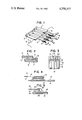
- FIG. 1 is a perspective view of a connection between a flexible printed circuit board and a hard printed circuit board in accordance with the present invention.
- FIG. 2 is an enlarged cross-sectional elevation view of one interconnection of the circuit boards of FIG. 1.
- FIG. 3 is a planar view of a flexible printed circuit board in accordance with another embodiment of the present invention.
- FIG. 4 is an enlarged cross-sectional view of the circuit board of FIG. 3 connected to a hard printed circuit board in accordance with a second embodiment of the method of the present invention.
- FIG. 5 is a cross-sectional elevation view of a connection, similar to FIG. 4, incorporating a reinforcement.
- a flexible printed circuit board shown generally at 1 is comprised of an insulating base material 2 with a printed circuit pattern 3 thereon.
- a rigid or hard circuit board shown generally at 6, is comprised of an insulating base material 7 with a circuit pattern 8 thereon.
- the circuit patterns are adhesively, mechanically and electrically interconnected by an electroconductive adhesive 4, as best seen in FIG. 2.
- the circuit elements 3 extend beyond the insulating base material 2, and the adhesive is initially applied to the underside of the elements 3.
- electroconductive adhesive 4 is applied to that portion of one or both circuit patterns to be connected.
- a visual alignment of the corresponding patterns is made and finally the circuit patterns 3 and 8 are physically brought together and pressed so as to physically join and electrically connect the circuit patterns of the two different printed circuit boards to each other.
- novel structure and connecting method of the present invention provides a simple and inexpensive approach to connecting flexible circuit boards to hardboards which has heretofore been accomplished only by sophisticated and/or technical procedures. Furthermore, unlike the prior connection techniques, with proper selection of adhesive material, the present invention allows for relatively easy removal of the adhesively connected circuit boards by various means of disengagement well known to those skilled in the art.
- FIGS. 3 and 4 a second embodiment of the present invention is shown wherein the end portion of the insulating base material 11 of flexible printed circuit board 10 is shaped like the teeth of a comb.
- the circuit patterns 12 which are attached to the base 11 extend out to the end of each particular tooth 11A at the end of the base 11.
- An electroconductive adhesive 13 is applied to both the top surface of the ends of the circuit pattern 12 and to the bottom base material surface of each tooth 11A of the base 11.
- the tooth structure of the base 11 of FIG. 3 is provided in order to prevent the adhesive 13 from short-circuiting adjoining circuit patterns 12.
- the teeth 11A are bent back upon themselves, as shown in FIG. 4, so that the adhesive applied to the bottom surface of the teeth 11A overlap and form a single integrated or overlapping structure.
- a hard circuit board 14 having an insulating base material 15 with circuit patterns 16 thereon can then be adhesively connected to the flexible circuit board 10.
- the respective circuit patterns 12 and 16 must be corresponding patterns. The connection is accomplished by visually matching up the respective circuit patterns 12 and 16 and subsequently pressing the patterns 12 and the patterns 16 into physical and electrical contact through the electroconductive adhesive 13.
- the present invention provides a structure and method of connection having low production cost, also being characterized by ease of separation if a problem arises in one of the connected circuit boards.
- the method of the present invention permits the connection between the respective, corresponding patterns to be reinforced by application of a nonelectroconductive adhesive tape over the adhesively connected patterns. This added reinforcement results in increased durability of the connection against vibration and other fatigue factors.
- FIG. 5 a connection according to FIG. 4 has been subsequently reinforced with solder 25.
- the circuit pattern 20 applied to insulating base material 19 of flexible circuit board 18 is adhesively connected by electroconductive adhesive 24 to the circuit pattern 23 on base material 22 of hardboard 21.
- the solder 25 acts to completely and more permanently connect the corresponding patterns 20 and 23.
- the circuit patterns of flexible and hard circuit boards can be simply and easily connected at low cost and little labor using an electroconductive adhesive. These adhesively connected patterns are then easily separable after the connection is obtained thereby providing an improved efficiency during inspections, part exchanges and repairs.
Abstract
Description
Claims (5)
Applications Claiming Priority (2)
| Application Number | Priority Date | Filing Date | Title |
|---|---|---|---|
| JP57113009A JPS594096A (en) | 1982-06-30 | 1982-06-30 | Method of connecting different type circuit boards to each other |
| JP57-113009 | 1982-06-30 |
Publications (1)
| Publication Number | Publication Date |
|---|---|
| US4550357A true US4550357A (en) | 1985-10-29 |
Family
ID=14601147
Family Applications (1)
| Application Number | Title | Priority Date | Filing Date |
|---|---|---|---|
| US06/508,281 Expired - Fee Related US4550357A (en) | 1982-06-30 | 1983-06-27 | Interconnected printed circuit boards and method of connecting circuit boards |
Country Status (5)
| Country | Link |
|---|---|
| US (1) | US4550357A (en) |
| JP (1) | JPS594096A (en) |
| CA (1) | CA1193370A (en) |
| DE (1) | DE3323469A1 (en) |
| GB (1) | GB2123224B (en) |
Cited By (16)
| Publication number | Priority date | Publication date | Assignee | Title |
|---|---|---|---|---|
| US4815981A (en) * | 1986-12-22 | 1989-03-28 | Teikoku Tsushin Kogyo Co., Ltd. | Flexible printed circuit board terminal structure |
| US4961806A (en) * | 1986-12-10 | 1990-10-09 | Sanders Associates, Inc. | Method of making a printed circuit |
| US5093761A (en) * | 1989-08-21 | 1992-03-03 | O.K Print Corporation | Circuit board device |
| US5097390A (en) * | 1986-12-10 | 1992-03-17 | Interflex Corporation | Printed circuit and fabrication of same |
| US5107078A (en) * | 1989-08-18 | 1992-04-21 | Commissariat A L'energie Atomique | Electric connection or disconnection element, integrated circuit including such elements and the corresponding connection or disconnection method |
| US5214571A (en) * | 1986-12-10 | 1993-05-25 | Miraco, Inc. | Multilayer printed circuit and associated multilayer material |
| US5278724A (en) * | 1992-07-06 | 1994-01-11 | International Business Machines Corporation | Electronic package and method of making same |
| US5283947A (en) * | 1992-02-10 | 1994-02-08 | Matsushita Electric Industrial Co., Inc. | Method of mounting electronic components on a circuit board |
| US5382829A (en) * | 1992-07-21 | 1995-01-17 | Mitsubishi Denki Kabushiki Kaisha | Packaged microwave semiconductor device |
| US5461202A (en) * | 1992-10-05 | 1995-10-24 | Matsushita Electric Industrial Co., Ltd. | Flexible wiring board and its fabrication method |
| US6353188B1 (en) * | 1997-02-05 | 2002-03-05 | Lear Corporation | Printed circuit assembly with flexible support |
| US6814588B1 (en) * | 2001-12-05 | 2004-11-09 | Adaptec, Inc. | Overmold cable terminator |
| US20050128717A1 (en) * | 2003-12-16 | 2005-06-16 | Toppoly Optoelectronics Corp. | Flexible printed circuit board(FPC) for liquid crystal display(LCD) module |
| US20090050354A1 (en) * | 2007-08-24 | 2009-02-26 | Foxconn Advanced Technology Inc. | Printed circuit board substrate and printed circuit board having the same |
| US20100054514A1 (en) * | 2008-08-27 | 2010-03-04 | Siemens Medical Instruments Pte. Ltd. | Electrical Circuit, Electrical Small Appliance, in Particular a Hearing Aid, Having the Electrical Circuit, and Use of the Electrical Circuit for Producing the Electrical Small Appliance |
| CN107359426A (en) * | 2017-06-29 | 2017-11-17 | 业成科技(成都)有限公司 | Electric connection structure and flexible circuit board |
Families Citing this family (11)
| Publication number | Priority date | Publication date | Assignee | Title |
|---|---|---|---|---|
| GB2155382B (en) * | 1982-08-03 | 1986-07-23 | Burroughs Corp | Stitch welding of wire to a printed circuit board |
| GB2155368B (en) * | 1982-08-03 | 1986-07-23 | Burroughs Corp | Method and apparatus for correcting printed circuit boards |
| DE3709306A1 (en) * | 1987-03-21 | 1988-09-29 | Mueller Rolf K Dr | PRESSURE SWITCHES, ESPECIALLY A KEYBOARD |
| DE3717306A1 (en) * | 1987-05-22 | 1988-12-01 | Ruf Kg Wilhelm | METHOD FOR PRODUCING AN ELECTRICAL CONTACT, AND CIRCUIT BOARD PRODUCED BY THE METHOD |
| US5502889A (en) * | 1988-06-10 | 1996-04-02 | Sheldahl, Inc. | Method for electrically and mechanically connecting at least two conductive layers |
| DE3905657A1 (en) * | 1989-02-24 | 1990-08-30 | Telefunken Electronic Gmbh | Flexible supporting film |
| US5727310A (en) * | 1993-01-08 | 1998-03-17 | Sheldahl, Inc. | Method of manufacturing a multilayer electronic circuit |
| US5428190A (en) * | 1993-07-02 | 1995-06-27 | Sheldahl, Inc. | Rigid-flex board with anisotropic interconnect and method of manufacture |
| US5527998A (en) | 1993-10-22 | 1996-06-18 | Sheldahl, Inc. | Flexible multilayer printed circuit boards and methods of manufacture |
| DE10011595A1 (en) * | 2000-03-10 | 2001-09-13 | Delphi Tech Inc | Joining a flexible printed circuit to a circuit of a circuit carrier used in the production of molded interconnected devices comprises using a conducting adhesive |
| JP5066779B2 (en) * | 2001-09-28 | 2012-11-07 | 日立化成工業株式会社 | Conductive paste and circuit connection method |
Citations (9)
| Publication number | Priority date | Publication date | Assignee | Title |
|---|---|---|---|---|
| US2854502A (en) * | 1956-12-05 | 1958-09-30 | Tape Cable Corp | Termination strip for electric cable |
| US3772776A (en) * | 1969-12-03 | 1973-11-20 | Thomas & Betts Corp | Method of interconnecting memory plane boards |
| US3836824A (en) * | 1972-10-24 | 1974-09-17 | Gen Electric | Mounting arrangement for flexible circuit |
| US4113981A (en) * | 1974-08-14 | 1978-09-12 | Kabushiki Kaisha Seikosha | Electrically conductive adhesive connecting arrays of conductors |
| US4180711A (en) * | 1976-09-14 | 1979-12-25 | Canon Kabushiki Kaisha | Desk-top calculator keyboard switch |
| US4203053A (en) * | 1978-01-24 | 1980-05-13 | Shepard Franziska M | Low voltage distribution system for miniature structure |
| US4251683A (en) * | 1979-04-23 | 1981-02-17 | Oak Industries, Inc. | Interconnect tail for a membrane switch |
| US4302065A (en) * | 1980-03-28 | 1981-11-24 | Western Electric Company, Incorporated | Flat cable assembly and methods of terminating and connectorizing the cable of same |
| US4457796A (en) * | 1981-06-25 | 1984-07-03 | Itt Industries | Permanently connecting a set of conductive tracks on a substrate with a co-operating set on a printed circuit |
Family Cites Families (7)
| Publication number | Priority date | Publication date | Assignee | Title |
|---|---|---|---|---|
| US3573345A (en) * | 1969-05-23 | 1971-04-06 | Rogers Corp | Connection of flexible printed circuit to connector board and method of making same |
| GB1477780A (en) * | 1974-08-14 | 1977-06-29 | Seikosha Kk | Assembly incorporating electrically conductive adhesive |
| JPS6044787B2 (en) * | 1977-11-09 | 1985-10-05 | 第一電子工業株式会社 | Conductive part connection method and conductive pressure sensitive adhesive |
| JPS5652885A (en) * | 1979-10-03 | 1981-05-12 | Shinetsu Polymer Co | Pressure nipping type connector |
| JPS5670529A (en) * | 1979-11-14 | 1981-06-12 | Hitachi Ltd | Liquid crystal display unit |
| GB2068645A (en) * | 1980-01-31 | 1981-08-12 | Rogers Corp | Electrical interconnection |
| NL8103303A (en) * | 1981-07-10 | 1983-02-01 | Philips Nv | COMPOSITE BODY. |
-
1982
- 1982-06-30 JP JP57113009A patent/JPS594096A/en active Pending
-
1983
- 1983-06-27 US US06/508,281 patent/US4550357A/en not_active Expired - Fee Related
- 1983-06-28 CA CA000431299A patent/CA1193370A/en not_active Expired
- 1983-06-29 DE DE19833323469 patent/DE3323469A1/en not_active Withdrawn
- 1983-06-30 GB GB08317809A patent/GB2123224B/en not_active Expired
Patent Citations (9)
| Publication number | Priority date | Publication date | Assignee | Title |
|---|---|---|---|---|
| US2854502A (en) * | 1956-12-05 | 1958-09-30 | Tape Cable Corp | Termination strip for electric cable |
| US3772776A (en) * | 1969-12-03 | 1973-11-20 | Thomas & Betts Corp | Method of interconnecting memory plane boards |
| US3836824A (en) * | 1972-10-24 | 1974-09-17 | Gen Electric | Mounting arrangement for flexible circuit |
| US4113981A (en) * | 1974-08-14 | 1978-09-12 | Kabushiki Kaisha Seikosha | Electrically conductive adhesive connecting arrays of conductors |
| US4180711A (en) * | 1976-09-14 | 1979-12-25 | Canon Kabushiki Kaisha | Desk-top calculator keyboard switch |
| US4203053A (en) * | 1978-01-24 | 1980-05-13 | Shepard Franziska M | Low voltage distribution system for miniature structure |
| US4251683A (en) * | 1979-04-23 | 1981-02-17 | Oak Industries, Inc. | Interconnect tail for a membrane switch |
| US4302065A (en) * | 1980-03-28 | 1981-11-24 | Western Electric Company, Incorporated | Flat cable assembly and methods of terminating and connectorizing the cable of same |
| US4457796A (en) * | 1981-06-25 | 1984-07-03 | Itt Industries | Permanently connecting a set of conductive tracks on a substrate with a co-operating set on a printed circuit |
Cited By (21)
| Publication number | Priority date | Publication date | Assignee | Title |
|---|---|---|---|---|
| US4961806A (en) * | 1986-12-10 | 1990-10-09 | Sanders Associates, Inc. | Method of making a printed circuit |
| US5097390A (en) * | 1986-12-10 | 1992-03-17 | Interflex Corporation | Printed circuit and fabrication of same |
| US5214571A (en) * | 1986-12-10 | 1993-05-25 | Miraco, Inc. | Multilayer printed circuit and associated multilayer material |
| US4815981A (en) * | 1986-12-22 | 1989-03-28 | Teikoku Tsushin Kogyo Co., Ltd. | Flexible printed circuit board terminal structure |
| US5107078A (en) * | 1989-08-18 | 1992-04-21 | Commissariat A L'energie Atomique | Electric connection or disconnection element, integrated circuit including such elements and the corresponding connection or disconnection method |
| US5093761A (en) * | 1989-08-21 | 1992-03-03 | O.K Print Corporation | Circuit board device |
| US5283947A (en) * | 1992-02-10 | 1994-02-08 | Matsushita Electric Industrial Co., Inc. | Method of mounting electronic components on a circuit board |
| US5278724A (en) * | 1992-07-06 | 1994-01-11 | International Business Machines Corporation | Electronic package and method of making same |
| US5534727A (en) * | 1992-07-21 | 1996-07-09 | Mitsubishi Denki Kabushiki Kaisha | Semiconductor device |
| US5382829A (en) * | 1992-07-21 | 1995-01-17 | Mitsubishi Denki Kabushiki Kaisha | Packaged microwave semiconductor device |
| US5461202A (en) * | 1992-10-05 | 1995-10-24 | Matsushita Electric Industrial Co., Ltd. | Flexible wiring board and its fabrication method |
| US6353188B1 (en) * | 1997-02-05 | 2002-03-05 | Lear Corporation | Printed circuit assembly with flexible support |
| US6814588B1 (en) * | 2001-12-05 | 2004-11-09 | Adaptec, Inc. | Overmold cable terminator |
| US20050128717A1 (en) * | 2003-12-16 | 2005-06-16 | Toppoly Optoelectronics Corp. | Flexible printed circuit board(FPC) for liquid crystal display(LCD) module |
| US7529100B2 (en) * | 2003-12-16 | 2009-05-05 | Tpo Displays Corp. | Flexible printed circuit board (FPC) for liquid crystal display (LCD) module |
| US20090050354A1 (en) * | 2007-08-24 | 2009-02-26 | Foxconn Advanced Technology Inc. | Printed circuit board substrate and printed circuit board having the same |
| US8089003B2 (en) * | 2007-08-24 | 2012-01-03 | Zhen Ding Technology Co., Ltd. | Printed circuit board assembly |
| US20100054514A1 (en) * | 2008-08-27 | 2010-03-04 | Siemens Medical Instruments Pte. Ltd. | Electrical Circuit, Electrical Small Appliance, in Particular a Hearing Aid, Having the Electrical Circuit, and Use of the Electrical Circuit for Producing the Electrical Small Appliance |
| EP2207406A3 (en) * | 2008-08-27 | 2010-09-08 | Siemens Medical Instruments Pte. Ltd. | Electrical switch, small electrical device, especially a hearing aid, with the electrical switch and use of the electrical switch to manufacture the small electrical device |
| CN107359426A (en) * | 2017-06-29 | 2017-11-17 | 业成科技(成都)有限公司 | Electric connection structure and flexible circuit board |
| CN107359426B (en) * | 2017-06-29 | 2021-12-07 | 业成科技(成都)有限公司 | Electric connection structure and flexible circuit board |
Also Published As
| Publication number | Publication date |
|---|---|
| GB2123224A (en) | 1984-01-25 |
| CA1193370A (en) | 1985-09-10 |
| JPS594096A (en) | 1984-01-10 |
| GB2123224B (en) | 1985-11-27 |
| GB8317809D0 (en) | 1983-08-03 |
| DE3323469A1 (en) | 1984-01-05 |
Similar Documents
| Publication | Publication Date | Title |
|---|---|---|
| US4550357A (en) | Interconnected printed circuit boards and method of connecting circuit boards | |
| EP0272707B1 (en) | Flexible printed circuit board terminal structure | |
| EP0658960A2 (en) | Cavity and bump interconnection structure for electronic packages | |
| JPS61140199A (en) | Manufacture of multilayer printed circuit board and multilayer printed circuit board manufacture thereby | |
| US4188714A (en) | Rigid termination for flexible printed circuits | |
| US5295838A (en) | Raised feature/gold dot pressure interconnections of rigid-flex circuits and rigid circuit boards | |
| US20040047136A1 (en) | Wiring board having terminal | |
| US5216358A (en) | Device for testing a printed circuit board | |
| US6739878B1 (en) | Pressure point contact for flexible cable | |
| JPH07288041A (en) | Flexible flat cable | |
| US3315133A (en) | Integrated circuit interconnect and method | |
| US6508664B2 (en) | Connectors for circuit boards configured with foil on both sides | |
| US5030110A (en) | Case assembly for stacking integrated circuit packages | |
| JPS6148997A (en) | Sheet having conductors printed on both sides and method of producing same | |
| JPH104248A (en) | Board connection structure | |
| US6291780B1 (en) | Method and device for connecting FPCs | |
| DE3641353C2 (en) | ||
| JPH05232142A (en) | Electric circuit having elastic gasket supporting body for uplifted contact | |
| JPH04116176U (en) | Connection structure of flexible printed wiring board | |
| JPH0342692Y2 (en) | ||
| JP3661261B2 (en) | Flat cable | |
| JPH0447905Y2 (en) | ||
| JPS63301587A (en) | Board connection structure | |
| JPS63273391A (en) | Coupling device for printed circuit board | |
| JP2517653Y2 (en) | Reinforcement structure for connecting terminals of flexible wiring board |
Legal Events
| Date | Code | Title | Description |
|---|---|---|---|
| AS | Assignment |
Owner name: NIPPON MEKTRON, LTD., 12-15, SHIBA DAIMON 1-CHOME, Free format text: ASSIGNMENT OF ASSIGNORS INTEREST.;ASSIGNOR:MATSUMOTO, HIROFUMI;REEL/FRAME:004147/0294 Effective date: 19830609 |
|
| FEPP | Fee payment procedure |
Free format text: PAYOR NUMBER ASSIGNED (ORIGINAL EVENT CODE: ASPN); ENTITY STATUS OF PATENT OWNER: LARGE ENTITY |
|
| REMI | Maintenance fee reminder mailed | ||
| FPAY | Fee payment |
Year of fee payment: 4 |
|
| SULP | Surcharge for late payment | ||
| REMI | Maintenance fee reminder mailed | ||
| LAPS | Lapse for failure to pay maintenance fees | ||
| FP | Lapsed due to failure to pay maintenance fee |
Effective date: 19931031 |
|
| FEPP | Fee payment procedure |
Free format text: PAYER NUMBER DE-ASSIGNED (ORIGINAL EVENT CODE: RMPN); ENTITY STATUS OF PATENT OWNER: LARGE ENTITY Free format text: PAYOR NUMBER ASSIGNED (ORIGINAL EVENT CODE: ASPN); ENTITY STATUS OF PATENT OWNER: LARGE ENTITY |
|
| STCH | Information on status: patent discontinuation |
Free format text: PATENT EXPIRED DUE TO NONPAYMENT OF MAINTENANCE FEES UNDER 37 CFR 1.362 |