US4535536A - Method of assembling adaptor for automatic testing equipment - Google Patents
Method of assembling adaptor for automatic testing equipment Download PDFInfo
- Publication number
- US4535536A US4535536A US06/548,422 US54842283A US4535536A US 4535536 A US4535536 A US 4535536A US 54842283 A US54842283 A US 54842283A US 4535536 A US4535536 A US 4535536A
- Authority
- US
- United States
- Prior art keywords
- plate
- apertures
- probes
- pattern
- ones
- Prior art date
- Legal status (The legal status is an assumption and is not a legal conclusion. Google has not performed a legal analysis and makes no representation as to the accuracy of the status listed.)
- Expired - Fee Related
Links
Images


Classifications
-
- H—ELECTRICITY
- H01—ELECTRIC ELEMENTS
- H01R—ELECTRICALLY-CONDUCTIVE CONNECTIONS; STRUCTURAL ASSOCIATIONS OF A PLURALITY OF MUTUALLY-INSULATED ELECTRICAL CONNECTING ELEMENTS; COUPLING DEVICES; CURRENT COLLECTORS
- H01R31/00—Coupling parts supported only by co-operation with counterpart
- H01R31/06—Intermediate parts for linking two coupling parts, e.g. adapter
-
- G—PHYSICS
- G01—MEASURING; TESTING
- G01R—MEASURING ELECTRIC VARIABLES; MEASURING MAGNETIC VARIABLES
- G01R1/00—Details of instruments or arrangements of the types included in groups G01R5/00 - G01R13/00 and G01R31/00
- G01R1/02—General constructional details
- G01R1/06—Measuring leads; Measuring probes
- G01R1/067—Measuring probes
- G01R1/073—Multiple probes
- G01R1/07307—Multiple probes with individual probe elements, e.g. needles, cantilever beams or bump contacts, fixed in relation to each other, e.g. bed of nails fixture or probe card
- G01R1/07364—Multiple probes with individual probe elements, e.g. needles, cantilever beams or bump contacts, fixed in relation to each other, e.g. bed of nails fixture or probe card with provisions for altering position, number or connection of probe tips; Adapting to differences in pitch
- G01R1/07371—Multiple probes with individual probe elements, e.g. needles, cantilever beams or bump contacts, fixed in relation to each other, e.g. bed of nails fixture or probe card with provisions for altering position, number or connection of probe tips; Adapting to differences in pitch using an intermediate card or back card with apertures through which the probes pass
-
- Y—GENERAL TAGGING OF NEW TECHNOLOGICAL DEVELOPMENTS; GENERAL TAGGING OF CROSS-SECTIONAL TECHNOLOGIES SPANNING OVER SEVERAL SECTIONS OF THE IPC; TECHNICAL SUBJECTS COVERED BY FORMER USPC CROSS-REFERENCE ART COLLECTIONS [XRACs] AND DIGESTS
- Y10—TECHNICAL SUBJECTS COVERED BY FORMER USPC
- Y10T—TECHNICAL SUBJECTS COVERED BY FORMER US CLASSIFICATION
- Y10T29/00—Metal working
- Y10T29/49—Method of mechanical manufacture
- Y10T29/49002—Electrical device making
- Y10T29/49117—Conductor or circuit manufacturing
- Y10T29/49124—On flat or curved insulated base, e.g., printed circuit, etc.
- Y10T29/49147—Assembling terminal to base
- Y10T29/49151—Assembling terminal to base by deforming or shaping
- Y10T29/49153—Assembling terminal to base by deforming or shaping with shaping or forcing terminal into base aperture
Definitions
- This invention is directed to the field of automatic testing equipment, and more particularly, to a novel adaptor for automatic testing equipment and method.
- Universal test fixtures for automatic testing equipment are commonly employed to removably retain an electronic circuit device in electrical communication with automatic testing equipment.
- the testing equipment is operative to ascertain whether the electronic circuit device conforms to a predetermined standard of quality whereby functional devices may be readily identified and separated from defective ones.
- the test fixtures usually include a regular array of upstanding signal contacts.
- the geometry defined by the electrical terminals of the electronic circuit device to be tested and the geometry defined by the regular array of upstanding signal contacts of the test fixture is often such that one or more of the electrical terminals of the circuit device are out of coaxial alignment with corresponding ones of the upstanding signal contacts of the test fixture.
- an adaptor is provided for electrically connecting the circuit device to the test head.
- One known adaptor includes an array of signal contacts aligned with the electrical terminals of the electronic circuit device to be tested that are individually hand-wired and soldered to preselected ones of an array of signal contacts having a geometry that corresponds to the geometry of the test fixture.
- hand-wired adaptors are disadvantageous, among other things, due to the considerable time and labor costs involved in hand-wiring the adaptors, and due to the possibility of erroneous results produced by a failure of one or more of the soldered electrical connections.
- an adaptor having an upper plate having apertures provided therethrough in alignment with the electrical terminals of an electronic circuit device to be tested, a lower plate having apertures provided therethrough corresponding to the regular array of signal contacts of the test fixture, and a plurality of flexible probes manually inserted between the plates such that the heads of the flexible probes define an array of contacts in alignment with the electrical terminals of the electronic circuit device to be tested and the tails of the flexible probes define a second array of signal contacts in alignment with the regular array of upstanding signal contacts on the test fixture.
- This type of adaptor is disadvantageous, among other things, due to the comparatively high cost of flexible probes.
- the tails of corresponding ones of the flexible probes are received in random ones of the apertures of the lower plate which necessitates that a particular adaptor configuration be "learned” by the automatic testing equipment on a known “good” device prior to testing for defective devices.
- the novel adaptor for automatic testing equipment of the present invention includes a plurality of rigid probes each having head and tail portions, and contemplates a probe support assembly and method that so disposes the rigid probes that the heads of the probes define a first array of signal contacts in alignment with the electrical terminals of a particular electronic circuit device and the tails of the probes define a second array of signal contacts in alignment with predetermined ones of the upstanding signal contacts of a universal test fixture.
- costly and time-consuming hand soldering, comparatively expensive flexible probes, as well as the "learning" procedure of the heretofore known adaptors are obviated.
- the novel adaptor for automatic testing equipment and method of the present invention preferably includes a top plate having apertures of a pre-selected size provided therethrough in a first pattern that conforms to the pattern of the electrical terminals of a particular electronic circuit device to be tested, a bottom plate having apertures having substantially the same size provided therethrough in a second pattern that conforms to the pattern of the upstanding signal contacts of a universal test head, and an alignment plate intermediate the top and bottom plate having apertures having an enlarged size in a third pattern that conforms to the first pattern of the electrical terminals of the electronic circuit device to be tested. Individual ones of the rigid probes are slidably received in confronting adjacent apertures through the several plates.
- the alignment plate is so positioned intermediate the top and bottom plates that those probes that are slidably received in coaxially aligned apertures of the top and bottom plates pass freely through the corresponding enlarged apertures of the intermediate plate into corresponding ones of the aligned apertures of the lower plate, while those probes that are slidably received in non-coaxially aligned apertures of the top and bottom plates are guided by the walls defining the corresponding apertures in the alignment plate into predetermined ones of the apertures in the lower plate.
- the novel method for fabricating the adaptor for automatic testing equipment includes the steps of spacing the top and alignment plates apart with each of the apertures of the top plate coaxially aligned with corresponding ones of the apertures of the alignment plate; inserting rigid probes through individual ones of the aligned apertures such that the head portions of each of the probes are disposed on the top plate and the tail portions thereof extend through the alignment plate; displacing the intermediate plate by a distance along a direction selected to align the tails of each of the rigid probes to be physically adjacent pre-selected ones of the apertures of the bottom plate; and controllably vibrating the alignment plate to allow the tails of each of the rigid probes to be received in the corresponding pre-selected ones of the apertures in the bottom plate.
- the rigid probe insertion step preferably includes the steps of placing a so-called egg crate assembly over the aligned top and alignment plates; disposing a plurality of rigid probes into the egg crate, and vibrating the egg crate and top and alignment plates in unison until such time as the probes are received in corresponding ones of the aligned apertures of the top and alignment plates.
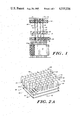
- FIG. 1 is a not-to-scale sectional view illustrating an adaptor for automatic testing equipment according to the present invention
- FIG. 2A is a not-to-scale exploded perspective view illustrating one step in the method of fabricating the adaptor for automatic testing equipment of the present invention
- FIG. 2B is a not-to-scale sectional view illustrating another step in the method of fabricating the adaptor for automatic testing equipment of the present invention
- FIG. 2C is a not-to-scale sectional view illustrating another step in the method of fabricating the adaptor for automatic testing equipment according to the present invention.
- FIG. 2D is a not-to-scale sectional view illustrating still another step in the method of fabricating the adaptor for automatic testing equipment according to the present invention.
- FIG. 2E is a not-to-scale sectional view illustrating another step in the method of fabricating the adapter for automatic testing equipment according to the present invention.
- FIG. 1 generally designated at 10 is a not-to-scale sectional view illustrating an adaptor for automatic testing equipment according to the present invention.
- the adaptor 10 electrically connects an electronic circuit device to be tested such as a printed circuit board 12 having a plurality of electrical terminals 14 to a test head 16 having a regular array of upstanding signal contacts 18.
- the contacts 18 are spring loaded POGO contacts.
- the adaptor 10 includes a top plate 20, an alignment plate 22, and a bottom plate 124 in vertically spaced relation.
- the top plate 20 includes a plurality of apertures 26 therethrough, five being specifically illustrated, each of which is coaxially aligned with a corresponding one of the electrical terminals 14 of the electronic circuit device 12 to be tested.
- the apertures 26 generally define a 2 ⁇ 2 array pattern that matches the 2 ⁇ 2 array pattern defined by the electrical terminals 14 of a particular device 12.
- the bottom plate 24 includes a plurality of apertures 28 therethrough, fourteen being specifically illustrated, each of which is coaxially aligned with a corresponding one of the upstanding signal contacts 18 of the test head 16 of the automatic testing equipment.
- the apertures 28 generally define a 2 ⁇ 2 array pattern that conforms to the 2 ⁇ 2 array pattern defined by the signal contacts 18 of the test head 16.
- the size of each of the apertures 26, 28 through the plates 20, 24 are preferably the same.
- the alignment plate 22 includes a plurality of apertures 30 therethrough, four being specifically illustrated, each of which is aligned with a corresponding one of the apertures 26 of the top plate 22.
- the apertures 30 each have a size selected to be larger than the size of the apertures 26, 28, and generally define a 2 ⁇ 2 array pattern that matches the 2 ⁇ 2 array pattern defined by the apertures 26 of the top plate 22.
- a plurality of rigid probes 32 are individually slidably received in corresponding pre-selected apertures 26, 28, 30 of the top, bottom, and alignment plates 20, 24, 22. Rigid probes are preferred although other probes, such as POGO probes can also be used.
- Each of the rigid probes 32 include an enlarged head portion 34 that is adapted to electrically contact corresponding ones of the electrical terminal 14 of the device 12, and a tail portion 36 that is adapted to electrically contact corresponding pre-selected ones of the corresponding signal contacts 18 of the head 16.
- Each of the rigid probes 32 pass through a corresponding one of the plurality of apertures 30 provided therefor in the allignment plate 22.
- the alignment plate 22 is so disposed intermediate the top plate 20 and the bottom plate 24 as to guide the tails 36 of the rigid probes 32 into pre-selected ones of the apertures 28 of the bottom plate 24.
- the alignment plate 22 In the case where a probe is received in aligned ones of the apertures 26, 28, as illustrated by the rigid probe 38, the alignment plate 22 so guides the probe that it is slidably received through the coaxially aligned aperture in the bottom plate. In the case where a probe is received in non-aligned ones of the apertures 26, 28, as illustrated by the rigid probe 40, the alignment plate 22 so guides the rigid probe that it is slidably received in a preselected one of the apertures in the bottom plate.
- the corresponding aperture pair of the top and bottom plates are aligned, and the rigid probes thereby pass through the aligned pairs in a generally vertical orientation; in the latter case, the corresponding aperture pairs of the top and bottom plates are not coaxially aligned, and the rigid probes are deflected by the walls of the corresponding apertures of the alignment plate out of vertical alignment such that the probes are selectively received in preselected apertures of the bottom plate.
- the assembly 42 includes a top plate 44 having a plurality of apertures 46 therethrough in a pattern that corresponds to the pattern defined by the electrical terminals of an electronic circuit device to be tested.
- An alignment plate 48 is provided below the top plate 44 having a plurality of apertures 50 therethrough that are coaxially aligned with the apertures 46 of the top plate 44.
- the apertures 46 of the top plate 44 are sized to be slightly larger than the cross-sectional diameter of the stems 45 (FIG.
- the rigid probes and the apertures 50 of the alignment plate 48 are sized to be larger than the apertures 46 to allow those rigid probes that extend between non-aligned aperture pairs of the top and bottom plates to deflect from the vertical.
- the top plate 44 and the alignment plate 48 are held in vertically spaced relation by any suitable means with individual ones of the openings 46 coaxially aligned with confronting corresponding ones of the openings 50.
- Alignment posts, illustrated by the dashed line 52 are preferably passed through aligned apertures 54 provided therefor on the corners of the top plate 44 and the alignment plate 48 for alignment of the assembly.
- An egg-crate generally designated 56 is positioned on the top plate 44.
- the egg-crate 56 includes a plurality of laterally and transversely extending spaced walls 58 and a plurality of laterally and transversely extending half-walls 60 spaced apart in the inter-spacing between the walls 58 along the width and length of the top plate 42.
- the walls 58 are preferably spaced apart a distance that is larger than the linear extension of the probes.
- the walls 58, 60 define a plurality of chambers generally designated 62 that are uniformly disposed over the top surface of the plate 44.
- a plurality of rigid probes 68 are poured into each of the chambers 66 in relative random orientation as shown in FIG. 2B.
- the spacing of the walls 58 and the height of the half-walls 60 prevents bridging of the probes therebetween so that all probes are received in corresponding chambers 66.
- the assembly 42 is vibrated in the horizontal plane as illustrated by the arrows 70 until each of the probes 68 are slidably received in corresponding ones of the aligned apertures of the top and alignment plate 44, 48.
- the egg-crate is then removed, and the excess probes are removed from the top plate.
- FIG. 2C generally designated at 68 in an assembly of components useful in illustrating another step in the method of fabricating the adaptor for automatic testing equipment according to the present invention.
- the alignment plate is displaced relative to the top plate in a generally downward direction by a distance "V,” and is moved generally horizontally by a distance "H” and in a direction selected to bring the tails of the probes 68 in position to be received in pre-selected ones of the apertures 70 provided in a bottom plate 72.
- the distance "H” is selected to correspond to the difference between the outside dimension of the stems of the probes 68 and the dimension of the apertures of the alignment plate.
- the direction preferably is selected to be 45°. In this manner, as appears below, the tail of a rigid probe designated 74 is selectively insertable in an aperture designated 76 in the bottom plate.
- the top plate 44 is lowered allowing the tails of the probes to contact the bottom plate 72.
- the alignment plate 48 is then vibrated for a controlled displacement in a generally circular pattern in the plane defined by the alignment plate as illustrated at 74 in FIG. 2E.
- the rigid probes 66 are thereby guided by the alignment plate 48 into pre-selected ones of the apertures provided therefor in the bottom plate 72.
- the probes slidably received in coxially aligned apertures of the top and bottom plates remain vertical, while the probes received in non-coaxially aligned apertures of the top and bottom plates are selectively guided by the intermediate plate into pre-selected apertures of the bottom plate.
- the rigid probes are received in pre-determined ones of the apertures of the bottom plate in a manner not requiring hand-soldering, flexible probes, nor the testing of a known "good” board to "learn” the configuration of a particular adaptor as in the heretofore known devices.
Abstract
Description
Claims (3)
Priority Applications (6)
| Application Number | Priority Date | Filing Date | Title |
|---|---|---|---|
| US06/548,422 US4535536A (en) | 1983-11-03 | 1983-11-03 | Method of assembling adaptor for automatic testing equipment |
| CA000466860A CA1209277A (en) | 1983-11-03 | 1984-11-01 | Adaptor for automatic testing equipment and method |
| EP84402202A EP0141747B1 (en) | 1983-11-03 | 1984-11-02 | Adaptor for automatic testing equipment and method |
| DE8484402202T DE3469116D1 (en) | 1983-11-03 | 1984-11-02 | Adaptor for automatic testing equipment and method |
| JP59233038A JPS60117579A (en) | 1983-11-03 | 1984-11-05 | Connecting adapter for electric circuit mechanism |
| US06/743,404 US4609243A (en) | 1983-11-03 | 1985-06-11 | Adaptor for automatic testing equipment |
Applications Claiming Priority (1)
| Application Number | Priority Date | Filing Date | Title |
|---|---|---|---|
| US06/548,422 US4535536A (en) | 1983-11-03 | 1983-11-03 | Method of assembling adaptor for automatic testing equipment |
Related Child Applications (1)
| Application Number | Title | Priority Date | Filing Date |
|---|---|---|---|
| US06/743,404 Division US4609243A (en) | 1983-11-03 | 1985-06-11 | Adaptor for automatic testing equipment |
Publications (1)
| Publication Number | Publication Date |
|---|---|
| US4535536A true US4535536A (en) | 1985-08-20 |
Family
ID=24188787
Family Applications (1)
| Application Number | Title | Priority Date | Filing Date |
|---|---|---|---|
| US06/548,422 Expired - Fee Related US4535536A (en) | 1983-11-03 | 1983-11-03 | Method of assembling adaptor for automatic testing equipment |
Country Status (5)
| Country | Link |
|---|---|
| US (1) | US4535536A (en) |
| EP (1) | EP0141747B1 (en) |
| JP (1) | JPS60117579A (en) |
| CA (1) | CA1209277A (en) |
| DE (1) | DE3469116D1 (en) |
Cited By (34)
| Publication number | Priority date | Publication date | Assignee | Title |
|---|---|---|---|---|
| US4633176A (en) * | 1984-06-20 | 1986-12-30 | Gte Communication Systems Corp. | Test fixture including deflectable probes |
| US4686465A (en) * | 1984-06-12 | 1987-08-11 | Feinmetall Gmbh | Probe assembly for circuit-board tester |
| US4686467A (en) * | 1984-03-21 | 1987-08-11 | Dit-Mco International Corp. | Circuit board testing system |
| US4707655A (en) * | 1984-06-12 | 1987-11-17 | Feinmetall Gmbh | Contact for multicontact probe assembly |
| US4736522A (en) * | 1985-08-08 | 1988-04-12 | Holaday Circuits, Inc. | Process for loading test pins |
| US4749943A (en) * | 1984-06-11 | 1988-06-07 | Thomas Black | Automatic test system |
| US4757254A (en) * | 1987-05-27 | 1988-07-12 | Augat Inc. | High-speed side access edge connector testing assembly |
| US4774459A (en) * | 1985-11-08 | 1988-09-27 | Martin Maelzer | Adapter for a printed circuit board testing apparatus |
| US4774462A (en) * | 1984-06-11 | 1988-09-27 | Black Thomas J | Automatic test system |
| US4788496A (en) * | 1982-11-05 | 1988-11-29 | Martin Maelzer | Adapter for a printed circuit board testing device |
| US4823079A (en) * | 1986-03-03 | 1989-04-18 | Siemens Aktiengesellschaft | Device for equipping an adapter with contact pins used with a circuit board test equipment |
| US4866375A (en) * | 1984-06-22 | 1989-09-12 | Malloy James T | Universal test fixture |
| US4899104A (en) * | 1986-11-18 | 1990-02-06 | Erich Luther | Adapter for a printed circuit board testing device |
| US4920636A (en) * | 1988-05-11 | 1990-05-01 | E. I. Du Pont De Nemours And Company | Pin alignment apparatus and method |
| US4926119A (en) * | 1988-03-04 | 1990-05-15 | Manfred Prokopp | Contact device for the testing of printed circuit boards or the like |
| US5285149A (en) * | 1990-02-16 | 1994-02-08 | Martin Maelzer | Method for loading an adapter for a device for testing printed circuit boards |
| US5394099A (en) * | 1992-02-04 | 1995-02-28 | Nhk Spring Co., Ltd. | Electroconductive contact probe with intermediately supported, spring urged converging needles having parallel free ends |
| US5414369A (en) * | 1992-11-09 | 1995-05-09 | Nhk Spring Co., Ltd. | Coil spring-pressed needle contact probe modules with offset needles |
| WO1995017681A1 (en) * | 1993-12-22 | 1995-06-29 | Methode Electronics, Inc. | Automatic probe fixture loading apparatus with gimballing compensation |
| US5511304A (en) * | 1992-07-30 | 1996-04-30 | Aksu; Allen | Automated test pin loading apparatus |
| US5600259A (en) * | 1993-12-17 | 1997-02-04 | International Business Machines Corporation | Method and apparatus for reducing interference in a pin array |
| US5694049A (en) * | 1993-09-17 | 1997-12-02 | Texas Instruments Incorporated | Socketless burn-in board |
| US5767692A (en) * | 1996-02-26 | 1998-06-16 | Circuit Line Spa | Device for converting the test point grid of a machine for electrically testing unassembled printed circuit boards |
| WO1999049325A1 (en) * | 1998-03-24 | 1999-09-30 | Nit Systems Ltd. | Automatic fixture building for electrical testing |
| US6407565B1 (en) | 1996-10-29 | 2002-06-18 | Agilent Technologies, Inc. | Loaded-board, guided-probe test fixture |
| US6414502B1 (en) | 1996-10-29 | 2002-07-02 | Agilent Technologies, Inc. | Loaded-board, guided-probe test fixture |
| US6437587B1 (en) | 1999-11-04 | 2002-08-20 | Agilent Technologies, Inc. | ICT test fixture for fine pitch testing |
| US20030234656A1 (en) * | 2002-06-25 | 2003-12-25 | Stephen Willard | Wireless test fixture adapter for printed circuit assembly tester |
| US20030234640A1 (en) * | 2002-06-24 | 2003-12-25 | Gregory Miczek | Method for producing a captive wired test fixture and fixture therefor |
| US20040128817A1 (en) * | 2002-12-13 | 2004-07-08 | Werner Lange | Method for the manufacture of fillings for utilization in the mechanical processing of aqueous paper fiber stock |
| US20040172816A1 (en) * | 2003-03-03 | 2004-09-09 | Youngman William Dale | Interconnect validation instruments |
| US20060129955A1 (en) * | 2004-12-10 | 2006-06-15 | Jacobsen Chris R | Printed circuit board development cycle using probe location automation and bead probe technology |
| KR100730390B1 (en) | 2006-06-15 | 2007-06-19 | (주) 현대테크 | Examination apparatus for Printed Circuit Board |
| US10060949B2 (en) * | 2016-08-24 | 2018-08-28 | Chunghwa Precision Test Tech. Co., Ltd. | Probe device of vertical probe card |
Families Citing this family (1)
| Publication number | Priority date | Publication date | Assignee | Title |
|---|---|---|---|---|
| EP0849599A1 (en) * | 1996-12-20 | 1998-06-24 | Lsi Logic Corporation | Apparatus for contacting semiconductor die |
Citations (7)
| Publication number | Priority date | Publication date | Assignee | Title |
|---|---|---|---|---|
| GB720908A (en) * | 1953-04-10 | 1954-12-29 | Kohnstam Ltd J | Improvements in or relating to electrical connectors |
| DE1800657A1 (en) * | 1968-10-02 | 1970-05-27 | Siemens Ag | Contact device, in particular for the electrical testing of the lines of printed or etched circuit boards in telecommunications technology |
| DE2063198A1 (en) * | 1969-12-22 | 1971-06-24 | Ibm | Electrical test equipment |
| DE2427118A1 (en) * | 1973-06-05 | 1975-01-23 | Siemens Ag | Adapter for testing printed circuit boards - has slotted contacting insert block and dowelled frame for board |
| DE2920226A1 (en) * | 1979-05-18 | 1980-11-20 | Siemens Ag | Coupling adaptor for testing circuit boards etc. - has perforated plate with loose contact needles, which has connecting template on side away from specimen |
| DE2933862A1 (en) * | 1979-08-21 | 1981-03-12 | Paul Mang | DEVICE FOR ELECTRONICALLY CHECKING CIRCUIT BOARDS. |
| DE3033717A1 (en) * | 1980-09-08 | 1982-03-18 | Siemens AG, 1000 Berlin und 8000 München | Printed circuit board test contact adaptor - has contacts overlapping four adjacent matrix points and eliminates adaptor adjustment |
Family Cites Families (2)
| Publication number | Priority date | Publication date | Assignee | Title |
|---|---|---|---|---|
| FR2524649A1 (en) * | 1982-04-02 | 1983-10-07 | Thomson Csf | Multiple contact printed circuit board testing system - uses set of feeler probes to form electrical contact with circuit board and second set of removable feeler probes |
| CH661129A5 (en) * | 1982-10-21 | 1987-06-30 | Feinmetall Gmbh | CONTACT DEVICE. |
-
1983
- 1983-11-03 US US06/548,422 patent/US4535536A/en not_active Expired - Fee Related
-
1984
- 1984-11-01 CA CA000466860A patent/CA1209277A/en not_active Expired
- 1984-11-02 EP EP84402202A patent/EP0141747B1/en not_active Expired
- 1984-11-02 DE DE8484402202T patent/DE3469116D1/en not_active Expired
- 1984-11-05 JP JP59233038A patent/JPS60117579A/en active Pending
Patent Citations (8)
| Publication number | Priority date | Publication date | Assignee | Title |
|---|---|---|---|---|
| GB720908A (en) * | 1953-04-10 | 1954-12-29 | Kohnstam Ltd J | Improvements in or relating to electrical connectors |
| DE1800657A1 (en) * | 1968-10-02 | 1970-05-27 | Siemens Ag | Contact device, in particular for the electrical testing of the lines of printed or etched circuit boards in telecommunications technology |
| DE2063198A1 (en) * | 1969-12-22 | 1971-06-24 | Ibm | Electrical test equipment |
| DE2427118A1 (en) * | 1973-06-05 | 1975-01-23 | Siemens Ag | Adapter for testing printed circuit boards - has slotted contacting insert block and dowelled frame for board |
| DE2920226A1 (en) * | 1979-05-18 | 1980-11-20 | Siemens Ag | Coupling adaptor for testing circuit boards etc. - has perforated plate with loose contact needles, which has connecting template on side away from specimen |
| DE2933862A1 (en) * | 1979-08-21 | 1981-03-12 | Paul Mang | DEVICE FOR ELECTRONICALLY CHECKING CIRCUIT BOARDS. |
| EP0026824A1 (en) * | 1979-08-21 | 1981-04-15 | Paul Mang | Adaptes for a device for electronically testing printed circuit boards |
| DE3033717A1 (en) * | 1980-09-08 | 1982-03-18 | Siemens AG, 1000 Berlin und 8000 München | Printed circuit board test contact adaptor - has contacts overlapping four adjacent matrix points and eliminates adaptor adjustment |
Non-Patent Citations (2)
| Title |
|---|
| IBM Tech. Discl. Bull., vol. 19, No. 1, Jun. 1976, p. 125 by J. Arnhart et al. * |
| IBM Tech. Discl. Bull., vol. 26, No. 1, Jun. 1983, p. 218 by M. Apgar et al. * |
Cited By (44)
| Publication number | Priority date | Publication date | Assignee | Title |
|---|---|---|---|---|
| US4788496A (en) * | 1982-11-05 | 1988-11-29 | Martin Maelzer | Adapter for a printed circuit board testing device |
| US4686467A (en) * | 1984-03-21 | 1987-08-11 | Dit-Mco International Corp. | Circuit board testing system |
| US4749943A (en) * | 1984-06-11 | 1988-06-07 | Thomas Black | Automatic test system |
| US4774462A (en) * | 1984-06-11 | 1988-09-27 | Black Thomas J | Automatic test system |
| US4686465A (en) * | 1984-06-12 | 1987-08-11 | Feinmetall Gmbh | Probe assembly for circuit-board tester |
| US4707655A (en) * | 1984-06-12 | 1987-11-17 | Feinmetall Gmbh | Contact for multicontact probe assembly |
| US4633176A (en) * | 1984-06-20 | 1986-12-30 | Gte Communication Systems Corp. | Test fixture including deflectable probes |
| US4866375A (en) * | 1984-06-22 | 1989-09-12 | Malloy James T | Universal test fixture |
| US4736522A (en) * | 1985-08-08 | 1988-04-12 | Holaday Circuits, Inc. | Process for loading test pins |
| US4774459A (en) * | 1985-11-08 | 1988-09-27 | Martin Maelzer | Adapter for a printed circuit board testing apparatus |
| US4823079A (en) * | 1986-03-03 | 1989-04-18 | Siemens Aktiengesellschaft | Device for equipping an adapter with contact pins used with a circuit board test equipment |
| US4899104A (en) * | 1986-11-18 | 1990-02-06 | Erich Luther | Adapter for a printed circuit board testing device |
| US4757254A (en) * | 1987-05-27 | 1988-07-12 | Augat Inc. | High-speed side access edge connector testing assembly |
| US4926119A (en) * | 1988-03-04 | 1990-05-15 | Manfred Prokopp | Contact device for the testing of printed circuit boards or the like |
| US4920636A (en) * | 1988-05-11 | 1990-05-01 | E. I. Du Pont De Nemours And Company | Pin alignment apparatus and method |
| US5285149A (en) * | 1990-02-16 | 1994-02-08 | Martin Maelzer | Method for loading an adapter for a device for testing printed circuit boards |
| US5357671A (en) * | 1990-02-16 | 1994-10-25 | Luther & Maelzer Gmbh | Device for loading an adapter for a device for testing printed circuit boards |
| US5394099A (en) * | 1992-02-04 | 1995-02-28 | Nhk Spring Co., Ltd. | Electroconductive contact probe with intermediately supported, spring urged converging needles having parallel free ends |
| US5511304A (en) * | 1992-07-30 | 1996-04-30 | Aksu; Allen | Automated test pin loading apparatus |
| US5414369A (en) * | 1992-11-09 | 1995-05-09 | Nhk Spring Co., Ltd. | Coil spring-pressed needle contact probe modules with offset needles |
| US5694049A (en) * | 1993-09-17 | 1997-12-02 | Texas Instruments Incorporated | Socketless burn-in board |
| US5600259A (en) * | 1993-12-17 | 1997-02-04 | International Business Machines Corporation | Method and apparatus for reducing interference in a pin array |
| US5453702A (en) * | 1993-12-22 | 1995-09-26 | Methode Electronics, Inc. | Automatic probe fixture loading apparatus with gimballing compensation |
| WO1995017681A1 (en) * | 1993-12-22 | 1995-06-29 | Methode Electronics, Inc. | Automatic probe fixture loading apparatus with gimballing compensation |
| US5767692A (en) * | 1996-02-26 | 1998-06-16 | Circuit Line Spa | Device for converting the test point grid of a machine for electrically testing unassembled printed circuit boards |
| US6407565B1 (en) | 1996-10-29 | 2002-06-18 | Agilent Technologies, Inc. | Loaded-board, guided-probe test fixture |
| US6414502B1 (en) | 1996-10-29 | 2002-07-02 | Agilent Technologies, Inc. | Loaded-board, guided-probe test fixture |
| US6469531B1 (en) | 1996-10-29 | 2002-10-22 | Agilent Technologies, Inc. | Loaded-board, guided-probe test fixture |
| WO1999049325A1 (en) * | 1998-03-24 | 1999-09-30 | Nit Systems Ltd. | Automatic fixture building for electrical testing |
| US6437587B1 (en) | 1999-11-04 | 2002-08-20 | Agilent Technologies, Inc. | ICT test fixture for fine pitch testing |
| US20060143909A1 (en) * | 2002-06-24 | 2006-07-06 | Gregory Miczek | Method for producing a captive wired test fixture and fixture therefor |
| US7424775B2 (en) | 2002-06-24 | 2008-09-16 | Delaware Capital Formation, Inc. | Captive wired test fixture |
| US20030234640A1 (en) * | 2002-06-24 | 2003-12-25 | Gregory Miczek | Method for producing a captive wired test fixture and fixture therefor |
| US7059046B2 (en) * | 2002-06-24 | 2006-06-13 | Delaware Capital Formation, Inc. | Method for producing a captive wired test fixture and fixture therefor |
| US20030234656A1 (en) * | 2002-06-25 | 2003-12-25 | Stephen Willard | Wireless test fixture adapter for printed circuit assembly tester |
| US6784675B2 (en) | 2002-06-25 | 2004-08-31 | Agilent Technologies, Inc. | Wireless test fixture adapter for printed circuit assembly tester |
| US7263755B2 (en) * | 2002-12-13 | 2007-09-04 | Voith Patent Gmbh | Method for the manufacture of fillings for utilization in the mechanical processing of aqueous paper fiber stock |
| US20040128817A1 (en) * | 2002-12-13 | 2004-07-08 | Werner Lange | Method for the manufacture of fillings for utilization in the mechanical processing of aqueous paper fiber stock |
| US7100273B2 (en) * | 2003-03-03 | 2006-09-05 | Hewlett-Packard Development Company, L.P. | Interconnect validation instruments |
| US20040172816A1 (en) * | 2003-03-03 | 2004-09-09 | Youngman William Dale | Interconnect validation instruments |
| US20060129955A1 (en) * | 2004-12-10 | 2006-06-15 | Jacobsen Chris R | Printed circuit board development cycle using probe location automation and bead probe technology |
| US20080148208A1 (en) * | 2004-12-10 | 2008-06-19 | Jacobsen Chris R | Method for improving a printed circuit board development cycle |
| KR100730390B1 (en) | 2006-06-15 | 2007-06-19 | (주) 현대테크 | Examination apparatus for Printed Circuit Board |
| US10060949B2 (en) * | 2016-08-24 | 2018-08-28 | Chunghwa Precision Test Tech. Co., Ltd. | Probe device of vertical probe card |
Also Published As
| Publication number | Publication date |
|---|---|
| JPS60117579A (en) | 1985-06-25 |
| EP0141747B1 (en) | 1988-01-27 |
| CA1209277A (en) | 1986-08-05 |
| DE3469116D1 (en) | 1988-03-03 |
| EP0141747A1 (en) | 1985-05-15 |
Similar Documents
| Publication | Publication Date | Title |
|---|---|---|
| US4535536A (en) | Method of assembling adaptor for automatic testing equipment | |
| CA1069598A (en) | Universally programmable shorting plug for an integrated circuit socket | |
| JPH022547B2 (en) | ||
| US4700132A (en) | Integrated circuit test site | |
| US4609243A (en) | Adaptor for automatic testing equipment | |
| US4744140A (en) | Alignment and insertion tool for connectors | |
| EP0135384B1 (en) | Probe head assembly | |
| JPS62182678A (en) | Test sight system | |
| US6012929A (en) | IC socket structure | |
| US4701703A (en) | Bed-of-pins test fixture | |
| CN212749137U (en) | Test apparatus with configurable probe fixture | |
| US5652523A (en) | Structure of IC device interface unit | |
| US5813869A (en) | IC socket and guide member | |
| US5276395A (en) | Bed-of-pins test fixture | |
| US4573756A (en) | Electrical interface arrangements | |
| JP2705332B2 (en) | IC device electrical characteristics measurement device | |
| JP3307166B2 (en) | Circuit board inspection equipment | |
| JP3094779B2 (en) | Circuit board inspection apparatus and inspection method | |
| JPH0631434Y2 (en) | Mounted board test jig | |
| KR19980081120A (en) | Electronic device and measuring method of the electronic device | |
| CA1169979A (en) | Multipin coupler | |
| US20020089322A1 (en) | Modular high parallelism interface for integrated circuit testing, method of assembly, and use of same | |
| JP2609860B2 (en) | Printed circuit board inspection jig pin | |
| JPH0138531Y2 (en) | ||
| JP3259355B2 (en) | IC device electrical characteristics measurement device |
Legal Events
| Date | Code | Title | Description |
|---|---|---|---|
| AS | Assignment |
Owner name: AUGAT INC., 89 FORBES BLVD., MANSFIELD, MA 02048 Free format text: ASSIGNMENT OF ASSIGNORS INTEREST.;ASSIGNOR:WYSS, ROBERT P.;REEL/FRAME:004192/0703 Effective date: 19831101 |
|
| AS | Assignment |
Owner name: ELECTRNIC SYSTEMS AND PROGRAMMING, INC., A MO CORP Free format text: ASSIGNMENT OF ASSIGNORS INTEREST.;ASSIGNOR:AUGAT, INC., A MA CORP;REEL/FRAME:004830/0844 Effective date: 19870630 Owner name: ELECTRNIC SYSTEMS AND PROGRAMMING, INC., A MO CORP Free format text: ASSIGNMENT OF ASSIGNORS INTEREST;ASSIGNOR:AUGAT, INC., A MA CORP;REEL/FRAME:004830/0844 Effective date: 19870630 |
|
| FEPP | Fee payment procedure |
Free format text: PAYOR NUMBER ASSIGNED (ORIGINAL EVENT CODE: ASPN); ENTITY STATUS OF PATENT OWNER: SMALL ENTITY |
|
| FPAY | Fee payment |
Year of fee payment: 4 |
|
| FEPP | Fee payment procedure |
Free format text: PAT HOLDER CLAIMS SMALL ENTITY STATUS - SMALL BUSINESS (ORIGINAL EVENT CODE: SM02); ENTITY STATUS OF PATENT OWNER: SMALL ENTITY Free format text: PAYER NUMBER DE-ASSIGNED (ORIGINAL EVENT CODE: RMPN); ENTITY STATUS OF PATENT OWNER: SMALL ENTITY Free format text: PAYOR NUMBER ASSIGNED (ORIGINAL EVENT CODE: ASPN); ENTITY STATUS OF PATENT OWNER: SMALL ENTITY |
|
| FPAY | Fee payment |
Year of fee payment: 8 |
|
| REMI | Maintenance fee reminder mailed | ||
| LAPS | Lapse for failure to pay maintenance fees | ||
| FP | Lapsed due to failure to pay maintenance fee |
Effective date: 19970820 |
|
| STCH | Information on status: patent discontinuation |
Free format text: PATENT EXPIRED DUE TO NONPAYMENT OF MAINTENANCE FEES UNDER 37 CFR 1.362 |