US4358890A - Process for making a dual implanted drain extension for bucket brigade device tetrode structure - Google Patents
Process for making a dual implanted drain extension for bucket brigade device tetrode structure Download PDFInfo
- Publication number
- US4358890A US4358890A US06/293,903 US29390381A US4358890A US 4358890 A US4358890 A US 4358890A US 29390381 A US29390381 A US 29390381A US 4358890 A US4358890 A US 4358890A
- Authority
- US
- United States
- Prior art keywords
- region
- diffusion
- threshold voltage
- bucket brigade
- channel region
- Prior art date
- Legal status (The legal status is an assumption and is not a legal conclusion. Google has not performed a legal analysis and makes no representation as to the accuracy of the status listed.)
- Expired - Fee Related
Links
- 238000000034 method Methods 0.000 title claims abstract description 19
- 230000008569 process Effects 0.000 title claims abstract description 18
- 230000009977 dual effect Effects 0.000 title description 14
- 238000009792 diffusion process Methods 0.000 claims abstract description 31
- 239000003990 capacitor Substances 0.000 claims abstract description 15
- 239000002019 doping agent Substances 0.000 claims abstract description 5
- VYPSYNLAJGMNEJ-UHFFFAOYSA-N Silicium dioxide Chemical compound O=[Si]=O VYPSYNLAJGMNEJ-UHFFFAOYSA-N 0.000 claims description 18
- 239000000758 substrate Substances 0.000 claims description 13
- 235000012239 silicon dioxide Nutrition 0.000 claims description 9
- 239000000377 silicon dioxide Substances 0.000 claims description 9
- 238000000151 deposition Methods 0.000 claims description 7
- 238000005468 ion implantation Methods 0.000 claims description 7
- 150000002500 ions Chemical class 0.000 claims description 6
- 239000004065 semiconductor Substances 0.000 claims description 6
- XUIMIQQOPSSXEZ-UHFFFAOYSA-N Silicon Chemical compound [Si] XUIMIQQOPSSXEZ-UHFFFAOYSA-N 0.000 claims description 3
- 229910052710 silicon Inorganic materials 0.000 claims description 3
- 239000010703 silicon Substances 0.000 claims description 3
- 230000000903 blocking effect Effects 0.000 claims 3
- 230000000873 masking effect Effects 0.000 claims 2
- 239000012212 insulator Substances 0.000 claims 1
- 238000012546 transfer Methods 0.000 abstract description 31
- 108091006146 Channels Proteins 0.000 abstract description 30
- 230000035945 sensitivity Effects 0.000 abstract description 5
- 108010075750 P-Type Calcium Channels Proteins 0.000 abstract description 3
- 210000004027 cell Anatomy 0.000 description 63
- 239000007943 implant Substances 0.000 description 21
- 238000003860 storage Methods 0.000 description 11
- 230000008901 benefit Effects 0.000 description 5
- 230000000694 effects Effects 0.000 description 5
- 230000006872 improvement Effects 0.000 description 5
- 229910052698 phosphorus Inorganic materials 0.000 description 5
- 239000011574 phosphorus Substances 0.000 description 5
- 239000005360 phosphosilicate glass Substances 0.000 description 5
- OAICVXFJPJFONN-UHFFFAOYSA-N Phosphorus Chemical compound [P] OAICVXFJPJFONN-UHFFFAOYSA-N 0.000 description 4
- 238000005530 etching Methods 0.000 description 4
- 238000004519 manufacturing process Methods 0.000 description 4
- 229910052751 metal Inorganic materials 0.000 description 4
- 239000002184 metal Substances 0.000 description 4
- 230000003071 parasitic effect Effects 0.000 description 4
- 229910052785 arsenic Inorganic materials 0.000 description 3
- RQNWIZPPADIBDY-UHFFFAOYSA-N arsenic atom Chemical compound [As] RQNWIZPPADIBDY-UHFFFAOYSA-N 0.000 description 3
- 238000010586 diagram Methods 0.000 description 3
- 230000005669 field effect Effects 0.000 description 3
- 230000003647 oxidation Effects 0.000 description 3
- 238000007254 oxidation reaction Methods 0.000 description 3
- 229920002120 photoresistant polymer Polymers 0.000 description 3
- 230000000644 propagated effect Effects 0.000 description 3
- 230000004888 barrier function Effects 0.000 description 2
- 230000008878 coupling Effects 0.000 description 2
- 238000010168 coupling process Methods 0.000 description 2
- 238000005859 coupling reaction Methods 0.000 description 2
- 238000002513 implantation Methods 0.000 description 2
- 229920006395 saturated elastomer Polymers 0.000 description 2
- 238000000926 separation method Methods 0.000 description 2
- 238000004904 shortening Methods 0.000 description 2
- 210000004460 N cell Anatomy 0.000 description 1
- WPPDFTBPZNZZRP-UHFFFAOYSA-N aluminum copper Chemical compound [Al].[Cu] WPPDFTBPZNZZRP-UHFFFAOYSA-N 0.000 description 1
- 238000013459 approach Methods 0.000 description 1
- 230000015556 catabolic process Effects 0.000 description 1
- 230000008859 change Effects 0.000 description 1
- 239000004020 conductor Substances 0.000 description 1
- 230000007423 decrease Effects 0.000 description 1
- 230000007547 defect Effects 0.000 description 1
- 238000006731 degradation reaction Methods 0.000 description 1
- 230000001419 dependent effect Effects 0.000 description 1
- 230000008021 deposition Effects 0.000 description 1
- 238000013461 design Methods 0.000 description 1
- 230000001627 detrimental effect Effects 0.000 description 1
- 238000005516 engineering process Methods 0.000 description 1
- 238000010884 ion-beam technique Methods 0.000 description 1
- 238000002955 isolation Methods 0.000 description 1
- 230000002093 peripheral effect Effects 0.000 description 1
- -1 phosphorus ions Chemical class 0.000 description 1
- 238000000206 photolithography Methods 0.000 description 1
- 229910021420 polycrystalline silicon Inorganic materials 0.000 description 1
- 238000012545 processing Methods 0.000 description 1
Images


Classifications
-
- H—ELECTRICITY
- H01—ELECTRIC ELEMENTS
- H01L—SEMICONDUCTOR DEVICES NOT COVERED BY CLASS H10
- H01L27/00—Devices consisting of a plurality of semiconductor or other solid-state components formed in or on a common substrate
- H01L27/02—Devices consisting of a plurality of semiconductor or other solid-state components formed in or on a common substrate including semiconductor components specially adapted for rectifying, oscillating, amplifying or switching and having at least one potential-jump barrier or surface barrier; including integrated passive circuit elements with at least one potential-jump barrier or surface barrier
- H01L27/04—Devices consisting of a plurality of semiconductor or other solid-state components formed in or on a common substrate including semiconductor components specially adapted for rectifying, oscillating, amplifying or switching and having at least one potential-jump barrier or surface barrier; including integrated passive circuit elements with at least one potential-jump barrier or surface barrier the substrate being a semiconductor body
- H01L27/10—Devices consisting of a plurality of semiconductor or other solid-state components formed in or on a common substrate including semiconductor components specially adapted for rectifying, oscillating, amplifying or switching and having at least one potential-jump barrier or surface barrier; including integrated passive circuit elements with at least one potential-jump barrier or surface barrier the substrate being a semiconductor body including a plurality of individual components in a repetitive configuration
- H01L27/105—Devices consisting of a plurality of semiconductor or other solid-state components formed in or on a common substrate including semiconductor components specially adapted for rectifying, oscillating, amplifying or switching and having at least one potential-jump barrier or surface barrier; including integrated passive circuit elements with at least one potential-jump barrier or surface barrier the substrate being a semiconductor body including a plurality of individual components in a repetitive configuration including field-effect components
- H01L27/1055—Devices consisting of a plurality of semiconductor or other solid-state components formed in or on a common substrate including semiconductor components specially adapted for rectifying, oscillating, amplifying or switching and having at least one potential-jump barrier or surface barrier; including integrated passive circuit elements with at least one potential-jump barrier or surface barrier the substrate being a semiconductor body including a plurality of individual components in a repetitive configuration including field-effect components comprising charge coupled devices of the so-called bucket brigade type
-
- H—ELECTRICITY
- H01—ELECTRIC ELEMENTS
- H01L—SEMICONDUCTOR DEVICES NOT COVERED BY CLASS H10
- H01L21/00—Processes or apparatus adapted for the manufacture or treatment of semiconductor or solid state devices or of parts thereof
- H01L21/70—Manufacture or treatment of devices consisting of a plurality of solid state components formed in or on a common substrate or of parts thereof; Manufacture of integrated circuit devices or of parts thereof
- H01L21/77—Manufacture or treatment of devices consisting of a plurality of solid state components or integrated circuits formed in, or on, a common substrate
- H01L21/78—Manufacture or treatment of devices consisting of a plurality of solid state components or integrated circuits formed in, or on, a common substrate with subsequent division of the substrate into plural individual devices
- H01L21/82—Manufacture or treatment of devices consisting of a plurality of solid state components or integrated circuits formed in, or on, a common substrate with subsequent division of the substrate into plural individual devices to produce devices, e.g. integrated circuits, each consisting of a plurality of components
- H01L21/822—Manufacture or treatment of devices consisting of a plurality of solid state components or integrated circuits formed in, or on, a common substrate with subsequent division of the substrate into plural individual devices to produce devices, e.g. integrated circuits, each consisting of a plurality of components the substrate being a semiconductor, using silicon technology
- H01L21/8232—Field-effect technology
- H01L21/8234—MIS technology, i.e. integration processes of field effect transistors of the conductor-insulator-semiconductor type
- H01L21/823406—Combination of charge coupled devices, i.e. CCD, or BBD
-
- H—ELECTRICITY
- H01—ELECTRIC ELEMENTS
- H01L—SEMICONDUCTOR DEVICES NOT COVERED BY CLASS H10
- H01L27/00—Devices consisting of a plurality of semiconductor or other solid-state components formed in or on a common substrate
- H01L27/02—Devices consisting of a plurality of semiconductor or other solid-state components formed in or on a common substrate including semiconductor components specially adapted for rectifying, oscillating, amplifying or switching and having at least one potential-jump barrier or surface barrier; including integrated passive circuit elements with at least one potential-jump barrier or surface barrier
- H01L27/04—Devices consisting of a plurality of semiconductor or other solid-state components formed in or on a common substrate including semiconductor components specially adapted for rectifying, oscillating, amplifying or switching and having at least one potential-jump barrier or surface barrier; including integrated passive circuit elements with at least one potential-jump barrier or surface barrier the substrate being a semiconductor body
- H01L27/06—Devices consisting of a plurality of semiconductor or other solid-state components formed in or on a common substrate including semiconductor components specially adapted for rectifying, oscillating, amplifying or switching and having at least one potential-jump barrier or surface barrier; including integrated passive circuit elements with at least one potential-jump barrier or surface barrier the substrate being a semiconductor body including a plurality of individual components in a non-repetitive configuration
- H01L27/07—Devices consisting of a plurality of semiconductor or other solid-state components formed in or on a common substrate including semiconductor components specially adapted for rectifying, oscillating, amplifying or switching and having at least one potential-jump barrier or surface barrier; including integrated passive circuit elements with at least one potential-jump barrier or surface barrier the substrate being a semiconductor body including a plurality of individual components in a non-repetitive configuration the components having an active region in common
- H01L27/0705—Devices consisting of a plurality of semiconductor or other solid-state components formed in or on a common substrate including semiconductor components specially adapted for rectifying, oscillating, amplifying or switching and having at least one potential-jump barrier or surface barrier; including integrated passive circuit elements with at least one potential-jump barrier or surface barrier the substrate being a semiconductor body including a plurality of individual components in a non-repetitive configuration the components having an active region in common comprising components of the field effect type
- H01L27/0727—Devices consisting of a plurality of semiconductor or other solid-state components formed in or on a common substrate including semiconductor components specially adapted for rectifying, oscillating, amplifying or switching and having at least one potential-jump barrier or surface barrier; including integrated passive circuit elements with at least one potential-jump barrier or surface barrier the substrate being a semiconductor body including a plurality of individual components in a non-repetitive configuration the components having an active region in common comprising components of the field effect type in combination with diodes, or capacitors or resistors
- H01L27/0733—Devices consisting of a plurality of semiconductor or other solid-state components formed in or on a common substrate including semiconductor components specially adapted for rectifying, oscillating, amplifying or switching and having at least one potential-jump barrier or surface barrier; including integrated passive circuit elements with at least one potential-jump barrier or surface barrier the substrate being a semiconductor body including a plurality of individual components in a non-repetitive configuration the components having an active region in common comprising components of the field effect type in combination with diodes, or capacitors or resistors in combination with capacitors only
-
- H—ELECTRICITY
- H01—ELECTRIC ELEMENTS
- H01L—SEMICONDUCTOR DEVICES NOT COVERED BY CLASS H10
- H01L29/00—Semiconductor devices adapted for rectifying, amplifying, oscillating or switching, or capacitors or resistors with at least one potential-jump barrier or surface barrier, e.g. PN junction depletion layer or carrier concentration layer; Details of semiconductor bodies or of electrodes thereof ; Multistep manufacturing processes therefor
- H01L29/02—Semiconductor bodies ; Multistep manufacturing processes therefor
- H01L29/06—Semiconductor bodies ; Multistep manufacturing processes therefor characterised by their shape; characterised by the shapes, relative sizes, or dispositions of the semiconductor regions ; characterised by the concentration or distribution of impurities within semiconductor regions
- H01L29/08—Semiconductor bodies ; Multistep manufacturing processes therefor characterised by their shape; characterised by the shapes, relative sizes, or dispositions of the semiconductor regions ; characterised by the concentration or distribution of impurities within semiconductor regions with semiconductor regions connected to an electrode carrying current to be rectified, amplified or switched and such electrode being part of a semiconductor device which comprises three or more electrodes
- H01L29/0843—Source or drain regions of field-effect devices
- H01L29/0847—Source or drain regions of field-effect devices of field-effect transistors with insulated gate
-
- H—ELECTRICITY
- H01—ELECTRIC ELEMENTS
- H01L—SEMICONDUCTOR DEVICES NOT COVERED BY CLASS H10
- H01L29/00—Semiconductor devices adapted for rectifying, amplifying, oscillating or switching, or capacitors or resistors with at least one potential-jump barrier or surface barrier, e.g. PN junction depletion layer or carrier concentration layer; Details of semiconductor bodies or of electrodes thereof ; Multistep manufacturing processes therefor
- H01L29/02—Semiconductor bodies ; Multistep manufacturing processes therefor
- H01L29/06—Semiconductor bodies ; Multistep manufacturing processes therefor characterised by their shape; characterised by the shapes, relative sizes, or dispositions of the semiconductor regions ; characterised by the concentration or distribution of impurities within semiconductor regions
- H01L29/10—Semiconductor bodies ; Multistep manufacturing processes therefor characterised by their shape; characterised by the shapes, relative sizes, or dispositions of the semiconductor regions ; characterised by the concentration or distribution of impurities within semiconductor regions with semiconductor regions connected to an electrode not carrying current to be rectified, amplified or switched and such electrode being part of a semiconductor device which comprises three or more electrodes
- H01L29/1025—Channel region of field-effect devices
- H01L29/1029—Channel region of field-effect devices of field-effect transistors
- H01L29/1033—Channel region of field-effect devices of field-effect transistors with insulated gate, e.g. characterised by the length, the width, the geometric contour or the doping structure
- H01L29/1041—Channel region of field-effect devices of field-effect transistors with insulated gate, e.g. characterised by the length, the width, the geometric contour or the doping structure with a non-uniform doping structure in the channel region surface
- H01L29/1045—Channel region of field-effect devices of field-effect transistors with insulated gate, e.g. characterised by the length, the width, the geometric contour or the doping structure with a non-uniform doping structure in the channel region surface the doping structure being parallel to the channel length, e.g. DMOS like
Landscapes
- Engineering & Computer Science (AREA)
- Power Engineering (AREA)
- Microelectronics & Electronic Packaging (AREA)
- Physics & Mathematics (AREA)
- Condensed Matter Physics & Semiconductors (AREA)
- General Physics & Mathematics (AREA)
- Computer Hardware Design (AREA)
- Ceramic Engineering (AREA)
- Manufacturing & Machinery (AREA)
- Solid State Image Pick-Up Elements (AREA)
Abstract
The invention is the structure and process for making a bucket brigade device which comprises the merger of an MOS capacitor with an MOSFET device to form the charge transfer cell. A first thin N-type region is implanted at a first concentration in a portion of the P-type channel region of an FET device adjacent to the drain diffusion. A second region is implanted with N-type dopant at a second concentration less than the first concentration, adjacent to and continuous with the first implanted region. The N-type concentration in the second region is just sufficient to compensate for the P-type background doping in the channel region. This structure increases the charge transfer efficiency for the cell and reduces its sensitivity of the threshold voltage to the source-drain voltage. The gate for the device has a substantial overlap over the drain and a minimal overlap over the source and the gate to drain capacitance per unit area is maximized by maintaining a uniformly thin oxide layer across the gate region.
Description
This is a division of application Ser. No. 99,362 filed Dec. 3, 1979, now abandoned, which is a continuation of application Ser. No. 938,679, filed Aug. 31, 1978, now abandoned.
The invention disclosed relates to semiconductor devices and fabrication processes and more particularly relates to an improvement in bucket brigade devices and processes for making same.
A bucket brigade circuit is a sequence of switching transistors interconnecting capacitive storage nodes, with the gates of alternate transistors in the sequence being driven by non-overlapping clock pulses. Bucket brigade circuits may be embodied advantageously in field effect transistor technology providing a bucket brigade cell which is simple in structure and manufacture. A voltage (charge) signal representative of the unit of binary information is introduced at the source of a first one of the FET bucket brigade cells. When the clock pulse on the gate of the first bucket brigade cell appears it bootstraps the previously restored drain node, causing current to flow through the FET device, and the unit of binary information is transferred to the storage capacitance between the first cell and the second cell. Thereafter, when the clock pulse on the gate of the second bucket brigade cell appears, the unit of binary information stored at the capacitive node between the first cell and the second cell is then transferred through the second cell to the restored capacitive node between the second cell and the third cell. In this manner, a voltage (charge) signal may be transferred through a string of bucket brigade cells using a two-phase clock to accomplish a serial storage, signal transfer, or signal processing operation. This operation is shown schematically in FIG. 1d. For each transfer there is always one cell which was initially empty of propagated charge. This empty cell is restored to a reference potential at the last device in a string and is essentially propagated in the reverse direction of information flow. Thus, for a two-phase clock, one needs 2 N cells to store N bits of information. The number of cells can be reduced to ##EQU1## for a multi (m) phase clock storing N bits of information.
A successful bucket brigade cell design must possess a number of attributes. Since bucket brigade cells are not used in isolation but are used in chain-like configurations, employing large numbers thereof, the cell must be of small dimension and be amenable to fabrication in high density integrated circuit arrangements. Since long chains of these cells are required for many applications, the transfer efficiency of each cell must be very close to unity and that transfer efficiency must not be different between that for the transfer of a binary zero signal and that for the transfer of a binary one signal.
A typical prior art implementation of a bucket brigade cell is shown in FIG. 1a with a cross-section of the cell along line 1b shown in FIG. 1b and a cross-section of the cell along the line 1c shown in FIG. 1c. The bucket brigade cell shown in FIGS. 1a-1c is of the metal gate type, which, although not having a self-aligned gate, utilizes a more simplified fabrication process than polycrystalline silicon self-aligned gate devices do, resulting in a more planar surface contour on which finer resolution photolithography can be performed. The prior art bucket brigade cell is formed as part of an integrated circuit in a P-type semiconductor substrate 2 and has an n+ type diffusion 4 which serves as its capacitive storage node. Under the thick oxide layer 6 in FIG. 1b, is the diffusion 4' whose right hand side serves as the source in the bucket brigade device 12 and whose left hand side serves as a portion of the drain for the bucket brigade device to the left of device 12. Generally, the prior art bucket brigade cell shown in FIG. 1b has a thick layer 6 of silicon dioxide which serves to separate the gates 12 and 14 of adjacent bucket brigade cells. Formed between the thick layers 6 of silicon dioxide is a thinner layer of silicon dioxide which consists of a relatively thinner portion 8 having a thickness typically on the order of 500 A to 1000 A and a relatively thicker portion 10 having a thickness generally on the order of 1000 A to 1500 A. The gate metal 12 of the bucket brigade cell is deposited and photolithographically delineated between the thick layers 6 of silicon dioxide over the thin oxide layers 8 and 10. Differential oxide thickness beneath the gate electrode 12 of a nonself-aligned gate FET device, in the region 3 between regions 6 and 8 of FIG. 1b, is desirable as taught in the prior art, to reduce parasitic capacitive coupling between the gate 12 and source 4' diffusion. Indeed, such devices are desired to be present on the LSI chip, which may also contain a bucket brigade chain, in order to perform other logical and input/output operations. The prior art process for forming the thicker region 3 relies on the enhanced oxidation rate of heavily doped silicon, such as the diffusion 4'. However, with this benefit comes the detriment of the growth of a corresponding thicker oxide layer 10 over the diffusion 4, which also reduces the capacitance between the gate 12 and the diffusion 4. The detrimental effect of this occurs when the FET device is employed as an element in a bucket brigade chain, since the charge storage node of the cell formed between the gate and diffusion will have a reduced capacitance per unit area.
The capacitive storage portion of the bucket brigade cell generally is located at the portion of the thin oxide layer 10 and the field effect switching portion of the bucket brigade cell is generally localized at the portion 8 of the thin oxide layer. This prior art bucket brigade cell suffers defects which are typical of the prior art. The prior art has not recognized nor solved the problem of including on the same IC chip both differential oxide FET logic devices and bucket brigade devices having a minimized thickness of the silicon dioxide layer 10 in the capacitive storage region, to maximize the capacitance per unit area thereof while at the same time maximizing the thickness of the oxide in region 3, in FIG. 1b, to minimize capacitive coupling to the source. Charge propagation along a bucket brigade chain as shown in FIG. 1d, is the result of a capacitive bootstrapping operation, where the magnitude of charge propagated from node-to-node is a function of the difference in magnitude between the gate-to-source capacitance Cgs and the gate-to-drain capacitance Cgd. The larger Cgd is with respect to Cgs, the larger will be the magnitude of the charge transferred. Since the minimum capacitance per bucket brigade cell is required to achieve a detectable output signal for a particular application, the cell must be made larger in area to meet the capacitance requirement.
Still other problems with the prior art bucket brigade cell, as is typified by that shown in FIG. 1a-1c, revolve about the inability to provide for self-alignment of the structural elements of the bucket brigade cell so that the spacing "X", which is required for alignment tolerance between the diffusion 4 and the gate oxide etching levels force the designer to make the separation distance "Y" wider between the diffusions 4a and 9 of devices in adjacent chains of bucket brigade cells. Still another set of problems associated with the prior art bucket brigade device cells concerns channel shortening effects which occur when adjacent cells within the same bucket brigade chain are brought too closely together. Because of the substantial vertical depth of the diffusion 4 in FIG. 1b as it faces the channel region between the diffusion 4 and the diffusion 4', as the separation distance between the diffusions 4 and 4' is reduced, the threshold voltage of the field effect transistor portion of the bucket brigade device beneath the thin oxide layer 8 becomes sensitive to the magnitude of the voltage difference between the diffusions 4 and 4'. This causes the threshold voltage, and therefore the charge transfer efficiency of the device to be different for binary one signals than it would be for binary zero signals. Since the threshold voltage and charge transfer efficiency has become dependent upon the logical value of the signal transferred, long chains of such bucket brigade cells will introduce a degradation in the signal transferred especially apparent in the first different bit in a sequence.
It is therefore an object of the invention to increase the circuit density of a bucket brigade device circuit.
It is another object of the invention to reduce the sensitivity of the threshold voltage of a bucket brigade device to the source-to-drain voltage magnitude.
It is yet another object of the invention to minimize the overlap capacitance of the gate to the source and maximize the overlap capacitance of the gate to the drain in the bucket brigade device.
It is still another object of the invention to reduce the short channel effect problems in a bucket brigade device.
It is yet a further object of the invention to provide, on the same IC chip, FET logic devices having reduced parasitic capacitances and bucket brigade devices having a maximized gate-to-drain capacitance per unit area.
These and other objects, features and advantages are accomplished by the improved bucket brigade device and process disclosed herein. The invention is the structure and process for making a bucket brigade device which comprises the merger of an MOS capacitor with an MOSFET device to form the charge transfer cell. A first thin N-type region 107 is implanted at a first concentration in a portion of the P-type channel region of an FET device adjacent to the drain diffusion. A second region 113 is implanted with N-type dopant at a second concentration less than the first concentration, adjacent to and continuous with the first implanted region. The N-type concentration in the second region is just sufficient to compensate for the P-type background doping in the channel region. This structure increases the charge transfer efficiency for the cell and reduces its sensitivity of the threshold voltage to the source-drain voltage. The gate for the device has a substantial overlap over the drain and a minimal overlap over the source and the gate to drain capacitance per unit area is maximized by maintaining a uniformly thin oxide layer across the gate region.
These and other objects, features and advantages of the invention will be more readily appreciated with reference to the accompanying figures.
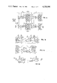
FIG. 1a is a plan view of a prior art bucket brigade device.
FIG. 1b is a cross-sectional view of FIG. 1a along line 1b.
FIG. 1c is a cross-sectional view of FIG. 1a along line 1c.
FIG. 1d is an electrical schematic diagram of the bucket brigade device chain of FIG. 1a.
FIG. 2a is a plan view of the invention showing the improved dual implant bucket brigade device with a double implanted drain extension.
FIG. 2b is a cross-sectional view of FIG. 2a along line 2b.
FIG. 2c is a cross-sectional view of FIG. 2a along line 2c.
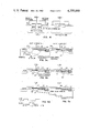
FIGS. 3a-3f illustrate the sequence of process steps necessary to fabricate the invention shown in FIG. 2a.
FIG. 4 illustrates high and low threshold voltage portions of FET device channel and bootstrap capacitor formed over ion-implanted storage node and electrical schematic of two cells in a bucket brigade device serial chain.
FIGS. 5a-5c illustrates, using potential well diagrams, the improvement in charge transfer efficiency due to dual implant structure.
FIG. 5d illustrates clock voltage waveform in charge transfer sequence of FIGS. 5a-5c.
FIG. 6 is a graphical representation of the relationship between transfer loss per stage versus the effective channel length for the dual implant bucket brigade device of FIG. 2a.
The invention is the structure and process for making a bucket brigade device which comprises the merger of an MOS capacitor with an MOSFET device to form the charge transfer cell. A first thin N-type region 107 in FIGS. 2a-2c, is implanted at a first concentration in a portion of the P-type channel region of an FET device adjacent to the drain diffusion. A second region 113 is implanted with N-type dopant at a second concentration less than the first concentration, adjacent to and continuous with the first implanted region. The N-type concentration in the second region is just sufficient to compensate for the P-type background doping in the channel region. This structure increases the charge transfer efficiency for the cell and reduces its sensitivity of the threshold voltage to the source-drain voltage. The gate for the device has a substantial overlap over the drain and a minimal overlap over the source and the gate to drain capacitance per unit area is maximized by maintaining a uniformly thin oxide layer across the gate region. The cell structure for the dual implant bucket brigade device invention is shown in FIGS. 2a-2c in two serially connected sequences of such cells, a first sequence of cells with first region 107 and second region 113 and a second sequence of cells with first region 111 and second region 115.
The cells are formed, as shown in FIGS. 3a-3f, as elements of an integrated circuit in a P-type semiconductor substrate 102 having a doping between 7-10×1015 /cm3. A source region 104 of opposite conductivity type (N-type) is formed by diffusion of phosphorus or arsenic in the surface of the substrate to a depth of 1-2 μm. A second similar drain region 104' for a second cell, is simultaneously formed spaced from the first source region 104. A thick silicon dioxide layer 106 is formed over the source regions 104 and 104' of thickness 8000 Angstroms. A thin oxide layer 110 having a uniform thickness of 500 A to 700 A is formed over the semiconductor substrate 102 in the region between the thick oxide layers 106 to form a serial chain of devices.
A portion of the thin oxide region 110 in each cell is subjected to the first ion-implantation of phosphorus or arsenic 133 in FIG. 3d which forms the drain electrode 107 of the FET device and the storage node of one plate of the thin oxide bootstrap capacitor. An implanted ion dose of 1-5×10¹³ /cm2 is sufficient to form the N-type layer 107 at less than 0.2 μm depth from the surface. This implanted region forms the drain 107 of the FET device, while the remaining portion of the substrate beneath the thin oxide region, between the implant 107 and the source diffusion 104' forms the FET device channel 105.
A second ion-implant 135 of FIG. 3e overlaps the first implanted region 107 and extends further into the thin oxide FET device channel region 105, forming the low threshold region 113. The second implantation 135 has a lower implant dose of 0.5-1×10¹² /cm2 of phosphorus or arsenic to compensate the substrate doping. The resulting device structure of FIG. 3f consists of two merged FET devices with different threshold voltages. The unimplanted region 109 of the channel 105 nearest the source 104' has a threshold voltage around 1 volt while the implanted region 113 near the implanted drain 107 has a lower threshold voltage between 0 and -1 volts.
A gate conductor 112 lies over the thin insulating layer 110 to complete the bucket brigade device structure of FIG. 3f.
Ions in the second ion-implant 135 can be used elsewhere in peripheral circuitry on the integrated circuit chip for well-known depletion load FET devices, for example.
The dual implant bucket brigade device cell formed with a merged charge storage capacitor and FET structure has several advantages: (1) The cell has a threshold voltage whose sensitivity to the source-to-drain potential is reduced yielding a high charge transfer efficiency. (2) The cell is very dense due to the superposition of the drain and thin oxide region which serves as the capacitor. And (3) The cell provides a large signal charge resulting from the maximum bootstrap capacitance due to the thin insulating layer in the implanted drain region and minimum parasitic capacitance due to thicker layers over the diffused regions. The process for making the dual implant bucket brigade device of FIGS. 2a-2c is shown in the FIGS. 3a-3f.
The process begins in the same manner as for the single implant device described in U.S. Pat. No. 4,142,199 by V. M. Simi, et al. entitled "Bucket Brigade Device and Process." The process commences in FIG. 3a by starting with a P-type silicon substrate 102 of approximately 1.5 ohm-centimeters (a doping concentration of 7-10×1015 /cm3) and growing an initial oxide layer 103 of 3000 A thickness, denoted as "a" in FIG. 3a, by a conventional thermal oxidation process. Windows 132 and 134 are then etched in the oxide layer 103. The source diffusions 104 and 104' are then formed in FIG. 3b by depositing phosphosilicate glass (PSG) over the thermal oxide layer 103 and the exposed windows 132 and 134 at a temperature of 870° C. for approximately twenty-five minutes. A source drive-in cycle of approximately 250 minutes in steam at 900° C. results in a 9500 A thickness of phosphosilicate glass over the source regions 104 and 104', denoted as "c", and a 7500 A thickness of silicon dioxide 136 over the remaining areas, denoted by "b", which results in a nearly planar surface for the resultant layer 136 of the phosphosilicate glass and silicon dioxide as shown in FIG. 3b.
Thereafter, a photo-oxide etching step is employed to form windows in the thick oxide structures between adjacent diffused regions, as shown in FIG. 3c. There is some intentionally introduced overlap of these windows over the diffusions to insure continuity between a diffusion and the thin oxide FET device channel to account for photoresist mask-to-mask alignments and tolerances. This overlap on the source diffusion defines the parasitic capacitance Cgs. The next step is an additional oxide growth step comprising 900° C.-250 minutes dry oxidation, 850° C.-10 minutes phosphosilicate glass deposition, and 1000° C.-20 minutes anneal to form the thin oxide layer 110, of thickness, 500 A, denoted as "d" in FIG. 3c.
The next step involves depositing a layer of photoresist 130 over a portion of the thin oxide layer 110 and the portion of an adjacent thick oxide structure 106 as shown in FIG. 3d, to serve as an ion-implantation mask for the implantation of phosphorus ions at 65 Kev. For a thin oxide layer 110 having a thickness of 500 Angstroms, a 65 Kev phosphorus ion beam exposure with 1013 /cm2 dose level will yield the N-type drain extension 107. This drain extension serves as the capacitive storage node for the device. For a 25fF bootstrap capacitor which is to store a typical 100fC signal charge, it occupies an area of 5×6 μm.
After the first ion-implantation mask 130 is removed, a second photoresist ion-implantation mask 140 is formed which exposes a larger area of thin oxide as shown in FIG. 3e. This second implant overlaps the drain extension 107 and exposes an additional 2-4 μm of the remaining thin oxide channel 105 between the diffusion 104' and drain 107.
FIG. 3e shows the second ion-implant of phosphorusions 135, forming the low threshold portion 113 of the FET device channel 105.
The second implant 135 as a dose level is substantially lower than the dose level of the first implant 133 such that the surface 113 forms a selectively invertible drain extension.
After removing the second mask 140 and forming a gate electrode 112 in the window, the improved bucket brigade device isformed having a dual implant as shown in FIG. 3f.
The final steps of the photo-oxide etching for contacts and depositing the metal gates 112 of aluminum-copper and etching the metal structures, completes the process.
This dual ion-implant device structure and process configuration permits substantial improvement in bucket brigade device shift register operation. The single implanted structure of copending U.S. Pat. No. 4,142,199 by V. M. Simi et al. assigned to the instant assignee, exhibits a density improvement due to the N-type drain extension aligned to the thin oxide bootstrap capacitor. The transfer efficiency of the single implanted device was also improved by the shallow depth of the drain extension which results in less short channel threshold voltage modulation with drain voltage. However, the new dual ion-implant structure disclosed herein provides the still further significant advantage ofa substantially better transfer efficiency due to even less threshold voltage variation of the combined high threshold voltage portion 109 and low threshold voltage portion 113 of the FET device channel 105. This can be represented as two serial FET devices as shown in FIG. 4. At high drain voltages the low threshold portion 113 of the channel 105 is depleted and the majority of the source-drain voltage is dropped across this portion as in standard pinch off operation (saturated mode). The threshold voltage for the combined devices is then governed by the high threshold portion 109 of the channel 105. Thus, any change in source-drain voltage does not appreciably effect the total device channel length and threshold as in uniform channel devices which suffer the well-known voltage induced channel shortening and short channel effect.
FIG. 5 shows another approach to illustrate the improvement in transfer efficiency with a dual implant bucket brigade device. The potential cell diagrams of two cells at various times in the transfer sequence are shown in FIGS. 5a-5c for non-overlapping two clock phases (FIG. 5d). Initially, (FIG. 5a) with clock 1 at a high voltage the signal charge (electrons) are concentrated in the high potential implanted drain extension 107 and N-type diffused region 104. During the transfer process the clock 1 voltage is reduced (FIG. 5b), lowering the potential of the signal charge. The high threshold portion 109 of the FET channel 105 acts as a barrier preventing charge from spilling into the previous cell. When clock 2 is at a high voltage (FIG. 5c) a deep potential well is formed in the drain extension of this second bucket brigade device cell and the high threshold portion of the channel is reduced allowing the signal charge to propagate into this next cell. It is desirable for high transfer efficiency, to keep this barrier region as narrow as possible to allow all the signal charge to diffuse and drift into the next cell independent of the source-drain potential. However, the well-known channel length modulation and short channel effects on threshold voltage can cause incomplete charge transfer on standard uniform channel devices. The dual implant structure essentially reduces this dependency, and as shown in FIG. 5c it allows the signal charge to transfer in several smaller steps with a more constant gradient which decreases the possibility of some residual charge becoming stuck in a corner of the previous cell.
FIG. 6 is a graphical representation of the relationship between the low frequency (100 KHz) transfer loss per stage versus the effective channel length for the dual implant bucket brigade device. This transfer loss is in reasonable agreement with the (αth) loss calculated from the measured variation in threshold voltage with drain-source voltage when operated in saturated mode. The gradient in potential across the dual FET structure also improves the transfer efficiency at high frequencies. With the shorter high threshold voltage portion of the channel required for good low frequency transfer efficiency, the conductance through the FET channel is increased which increases the rate of charge transfer for good efficiency at higher operating frequencies.
While the invention has been particularly shown and described with reference to the preferred embodiment thereof, it will be understood by those skilled in the art that the foregoing and other changes in form and detail may be made therein without departing from the spirit and scope of the invention.
Claims (1)
1. A process for making a serially connected plurality of bucket brigade devices in a silicon semiconductor substrate of P-type conductivity and a dopant concentration of from 7 to 10×1015 /cm3, each of said devices occupying a device area bounded on opposed ends by a first and a second diffusion of N-type conductivity, the first diffusion of a first device serving as the second diffusion of a next serially connected device, with a thick insulating layer overlying said semiconductor substrate having a plurality of windows therethrough, each said window juxtaposed over and exposing a corresponding one of said device areas, comprising the steps of:
growing a thin insulating layer of silicon dioxide on the surface of said substrate in each of said device areas, to a thickness of from 500 A to 700 A;
depositing a first ion implantation blocking mask over a first portion of each of said device areas, masking a channel region adjacent to said first diffusion and exposing a capacitor plate region adjacent to said second diffusion, said first mask having an edge defining the boundary between said channel region and said capacitor plate region;
ion implanting N-type conductivity dopant ions at an energy of 65 Kev and a first dose of from 1 to 5×10¹³ /cm2 through said thin insulating layer and into said substrate in said capacitor plate region of each of said device areas, forming an N-type conductivity capacitor plate in said substrate which has a terminal edge at said boundary between said channel region and said plate region and which electrically contacts said second diffusion;
removing said first ion implantation blocking mask and depositing a second ion implantation blocking mask over a second portion of each of said device areas, masking a first, high threshold voltage portion of said channel region adjacent to said first diffusion and exposing a second, low threshold voltage portion of said channel region adjacent to said terminal edge of said capacitor plate;
ion implanting said N-type conductivity ions at a second dose of from 0.5 to 1×10¹² /cm2, which is lower than said first dose, through said thin insulating layer and into said substrate in said low threshold voltage portion of said channel region, forming an N-type conductivity doped low threshold voltage region having a threshold voltage of between 0 and -1 volts;
said high threshold voltage portion of said channel region having a threshold voltage of approximately +1 volts;
removing said second mask and depositing a gate electrode on said thin insulator layer over said channel region and said capacitor plate region in each of said device areas;
whereby an improved, serially connected plurality of bucket brigade devices is formed.
Priority Applications (1)
| Application Number | Priority Date | Filing Date | Title |
|---|---|---|---|
| US06/293,903 US4358890A (en) | 1978-08-31 | 1981-08-18 | Process for making a dual implanted drain extension for bucket brigade device tetrode structure |
Applications Claiming Priority (2)
| Application Number | Priority Date | Filing Date | Title |
|---|---|---|---|
| US93867978A | 1978-08-31 | 1978-08-31 | |
| US06/293,903 US4358890A (en) | 1978-08-31 | 1981-08-18 | Process for making a dual implanted drain extension for bucket brigade device tetrode structure |
Related Parent Applications (1)
| Application Number | Title | Priority Date | Filing Date |
|---|---|---|---|
| US06099362 Division | 1979-12-03 |
Publications (1)
| Publication Number | Publication Date |
|---|---|
| US4358890A true US4358890A (en) | 1982-11-16 |
Family
ID=26968222
Family Applications (1)
| Application Number | Title | Priority Date | Filing Date |
|---|---|---|---|
| US06/293,903 Expired - Fee Related US4358890A (en) | 1978-08-31 | 1981-08-18 | Process for making a dual implanted drain extension for bucket brigade device tetrode structure |
Country Status (1)
| Country | Link |
|---|---|
| US (1) | US4358890A (en) |
Cited By (6)
| Publication number | Priority date | Publication date | Assignee | Title |
|---|---|---|---|---|
| JPS60170968A (en) * | 1984-02-15 | 1985-09-04 | Sony Corp | Vertical type overflow image sensor |
| US4956311A (en) * | 1989-06-27 | 1990-09-11 | National Semiconductor Corporation | Double-diffused drain CMOS process using a counterdoping technique |
| US5065203A (en) * | 1988-07-07 | 1991-11-12 | Tektronix, Inc. | Trench structured charge-coupled device |
| US5399513A (en) * | 1989-06-27 | 1995-03-21 | National Semiconductor Corporation | Salicide compatible CMOS process with a differential oxide implant mask |
| US5496761A (en) * | 1992-04-17 | 1996-03-05 | Sgs-Thomson Microelectronics S.R.L. | Method of making junction-isolated high voltage MOS integrated device |
| US20170170311A1 (en) * | 2015-12-10 | 2017-06-15 | Taiwan Semiconductor Manufacturing Company Ltd. | High voltage ldmos transistor and methods for manufacturing the same |
Citations (6)
| Publication number | Priority date | Publication date | Assignee | Title |
|---|---|---|---|---|
| US3767983A (en) * | 1972-08-23 | 1973-10-23 | Bell Telephone Labor Inc | Charge transfer device with improved transfer efficiency |
| US3789267A (en) * | 1971-06-28 | 1974-01-29 | Bell Telephone Labor Inc | Charge coupled devices employing nonuniform concentrations of immobile charge along the information channel |
| US4087832A (en) * | 1976-07-02 | 1978-05-02 | International Business Machines Corporation | Two-phase charge coupled device structure |
| US4100513A (en) * | 1975-09-18 | 1978-07-11 | Reticon Corporation | Semiconductor filtering apparatus |
| US4142199A (en) * | 1977-06-24 | 1979-02-27 | International Business Machines Corporation | Bucket brigade device and process |
| US4771229A (en) * | 1986-06-13 | 1988-09-13 | Siemens Aktiengesellschaft | Circuit arrangement for automatic connection of the remote feed current paths of a remote feed loop |
-
1981
- 1981-08-18 US US06/293,903 patent/US4358890A/en not_active Expired - Fee Related
Patent Citations (6)
| Publication number | Priority date | Publication date | Assignee | Title |
|---|---|---|---|---|
| US3789267A (en) * | 1971-06-28 | 1974-01-29 | Bell Telephone Labor Inc | Charge coupled devices employing nonuniform concentrations of immobile charge along the information channel |
| US3767983A (en) * | 1972-08-23 | 1973-10-23 | Bell Telephone Labor Inc | Charge transfer device with improved transfer efficiency |
| US4100513A (en) * | 1975-09-18 | 1978-07-11 | Reticon Corporation | Semiconductor filtering apparatus |
| US4087832A (en) * | 1976-07-02 | 1978-05-02 | International Business Machines Corporation | Two-phase charge coupled device structure |
| US4142199A (en) * | 1977-06-24 | 1979-02-27 | International Business Machines Corporation | Bucket brigade device and process |
| US4771229A (en) * | 1986-06-13 | 1988-09-13 | Siemens Aktiengesellschaft | Circuit arrangement for automatic connection of the remote feed current paths of a remote feed loop |
Cited By (13)
| Publication number | Priority date | Publication date | Assignee | Title |
|---|---|---|---|---|
| JPS60170968A (en) * | 1984-02-15 | 1985-09-04 | Sony Corp | Vertical type overflow image sensor |
| US5065203A (en) * | 1988-07-07 | 1991-11-12 | Tektronix, Inc. | Trench structured charge-coupled device |
| US4956311A (en) * | 1989-06-27 | 1990-09-11 | National Semiconductor Corporation | Double-diffused drain CMOS process using a counterdoping technique |
| US5399513A (en) * | 1989-06-27 | 1995-03-21 | National Semiconductor Corporation | Salicide compatible CMOS process with a differential oxide implant mask |
| US5496761A (en) * | 1992-04-17 | 1996-03-05 | Sgs-Thomson Microelectronics S.R.L. | Method of making junction-isolated high voltage MOS integrated device |
| CN106876462A (en) * | 2015-12-10 | 2017-06-20 | 台湾积体电路制造股份有限公司 | High-voltage LDMOS transistor and its manufacture method |
| US20170170311A1 (en) * | 2015-12-10 | 2017-06-15 | Taiwan Semiconductor Manufacturing Company Ltd. | High voltage ldmos transistor and methods for manufacturing the same |
| US9911845B2 (en) * | 2015-12-10 | 2018-03-06 | Taiwan Semiconductor Manufacturing Company, Ltd. | High voltage LDMOS transistor and methods for manufacturing the same |
| TWI635542B (en) * | 2015-12-10 | 2018-09-11 | 台灣積體電路製造股份有限公司 | High voltage ldmos transistor and methods for manufacturing the same |
| DE102016100128B4 (en) * | 2015-12-10 | 2020-04-09 | Taiwan Semiconductor Manufacturing Company, Ltd. | High-voltage LDMOS transistor and method for its production |
| US10790387B2 (en) * | 2015-12-10 | 2020-09-29 | Taiwan Semiconductor Manufacturing Company Ltd. | High voltage LDMOS transistor and methods for manufacturing the same |
| CN106876462B (en) * | 2015-12-10 | 2020-11-13 | 台湾积体电路制造股份有限公司 | High-voltage LDMOS transistor and manufacturing method thereof |
| US10930776B2 (en) | 2015-12-10 | 2021-02-23 | Taiwan Semiconductor Manufacturing Company Ltd. | High voltage LDMOS transistor and methods for manufacturing the same |
Similar Documents
| Publication | Publication Date | Title |
|---|---|---|
| US4825278A (en) | Radiation hardened semiconductor devices | |
| US4899202A (en) | High performance silicon-on-insulator transistor with body node to source node connection | |
| US4701776A (en) | MOS floating gate memory cell and process for fabricating same | |
| US4822750A (en) | MOS floating gate memory cell containing tunneling diffusion region in contact with drain and extending under edges of field oxide | |
| US4065783A (en) | Self-aligned double implanted short channel V-groove MOS device | |
| US4160987A (en) | Field effect transistors with polycrystalline silicon gate self-aligned to both conductive and non-conductive regions and fabrication of integrated circuits containing the transistors | |
| US4047215A (en) | Uniphase charge coupled devices | |
| US4280855A (en) | Method of making a dual DMOS device by ion implantation and diffusion | |
| US4101921A (en) | Memory type insulating gate field effect semiconductor device | |
| WO1981000931A1 (en) | Cmos p-well selective implant method,and a device made therefrom | |
| US4454524A (en) | Device having implantation for controlling gate parasitic action | |
| US4316203A (en) | Insulated gate field effect transistor | |
| US6656803B2 (en) | Radiation hardened semiconductor memory | |
| US4229756A (en) | Ultra high speed complementary MOS device | |
| US4131907A (en) | Short-channel V-groove complementary MOS device | |
| KR100394425B1 (en) | A channel stop method for use in a thick field isolation region in a triple well structure | |
| JP3470133B2 (en) | Method for manufacturing semiconductor device | |
| GB1563863A (en) | Igfet inverters and methods of fabrication thereof | |
| US4484209A (en) | SOS Mosfet with thinned channel contact region | |
| US4481527A (en) | High density MNOS transistor with ion implant into nitride layer adjacent gate electrode | |
| US4358890A (en) | Process for making a dual implanted drain extension for bucket brigade device tetrode structure | |
| US4142199A (en) | Bucket brigade device and process | |
| US3852119A (en) | Metal-insulator-semiconductor structures having reduced junction capacitance and method of fabrication | |
| US3906542A (en) | Conductively connected charge coupled devices | |
| EP0070744B1 (en) | Insulated gate field effect transistor |
Legal Events
| Date | Code | Title | Description |
|---|---|---|---|
| MAFP | Maintenance fee payment |
Free format text: PAYMENT OF MAINTENANCE FEE, 4TH YEAR, PL 96-517 (ORIGINAL EVENT CODE: M170); ENTITY STATUS OF PATENT OWNER: LARGE ENTITY Year of fee payment: 4 |
|
| FEPP | Fee payment procedure |
Free format text: MAINTENANCE FEE REMINDER MAILED (ORIGINAL EVENT CODE: REM.); ENTITY STATUS OF PATENT OWNER: LARGE ENTITY |
|
| LAPS | Lapse for failure to pay maintenance fees | ||
| STCH | Information on status: patent discontinuation |
Free format text: PATENT EXPIRED DUE TO NONPAYMENT OF MAINTENANCE FEES UNDER 37 CFR 1.362 |
|
| FP | Lapsed due to failure to pay maintenance fee |
Effective date: 19901118 |