US4309225A - Method of crystallizing amorphous material with a moving energy beam - Google Patents
Method of crystallizing amorphous material with a moving energy beam Download PDFInfo
- Publication number
- US4309225A US4309225A US06/123,745 US12374580A US4309225A US 4309225 A US4309225 A US 4309225A US 12374580 A US12374580 A US 12374580A US 4309225 A US4309225 A US 4309225A
- Authority
- US
- United States
- Prior art keywords
- amorphous
- film
- crystallization
- laser
- energy
- Prior art date
- Legal status (The legal status is an assumption and is not a legal conclusion. Google has not performed a legal analysis and makes no representation as to the accuracy of the status listed.)
- Expired - Lifetime
Links
- 238000000034 method Methods 0.000 title claims abstract description 70
- 239000000463 material Substances 0.000 title claims abstract description 66
- 238000002425 crystallisation Methods 0.000 claims abstract description 67
- 230000008025 crystallization Effects 0.000 claims abstract description 67
- 239000004065 semiconductor Substances 0.000 claims description 82
- 239000000758 substrate Substances 0.000 claims description 34
- GNPVGFCGXDBREM-UHFFFAOYSA-N germanium atom Chemical compound [Ge] GNPVGFCGXDBREM-UHFFFAOYSA-N 0.000 claims description 23
- 229910052732 germanium Inorganic materials 0.000 claims description 20
- 230000000737 periodic effect Effects 0.000 claims description 18
- 238000002844 melting Methods 0.000 claims description 14
- 230000009466 transformation Effects 0.000 claims description 14
- 230000008018 melting Effects 0.000 claims description 13
- 238000004519 manufacturing process Methods 0.000 claims description 10
- VYPSYNLAJGMNEJ-UHFFFAOYSA-N Silicium dioxide Chemical compound O=[Si]=O VYPSYNLAJGMNEJ-UHFFFAOYSA-N 0.000 claims description 9
- 238000010894 electron beam technology Methods 0.000 claims description 9
- 238000010438 heat treatment Methods 0.000 claims description 8
- 239000007790 solid phase Substances 0.000 claims description 8
- JBRZTFJDHDCESZ-UHFFFAOYSA-N AsGa Chemical compound [As]#[Ga] JBRZTFJDHDCESZ-UHFFFAOYSA-N 0.000 claims description 7
- 229910001218 Gallium arsenide Inorganic materials 0.000 claims description 7
- 229910021417 amorphous silicon Inorganic materials 0.000 claims description 7
- 239000002178 crystalline material Substances 0.000 claims description 7
- 238000000151 deposition Methods 0.000 claims description 7
- 238000010884 ion-beam technique Methods 0.000 claims description 6
- 230000006872 improvement Effects 0.000 claims description 5
- 239000007787 solid Substances 0.000 claims description 3
- 229910000927 Ge alloy Inorganic materials 0.000 claims description 2
- 229910000676 Si alloy Inorganic materials 0.000 claims description 2
- 239000011248 coating agent Substances 0.000 claims description 2
- 238000000576 coating method Methods 0.000 claims description 2
- TWNQGVIAIRXVLR-UHFFFAOYSA-N oxo(oxoalumanyloxy)alumane Chemical compound O=[Al]O[Al]=O TWNQGVIAIRXVLR-UHFFFAOYSA-N 0.000 claims description 2
- 239000000377 silicon dioxide Substances 0.000 claims description 2
- 235000012239 silicon dioxide Nutrition 0.000 claims description 2
- 229910010272 inorganic material Inorganic materials 0.000 claims 3
- 239000011147 inorganic material Substances 0.000 claims 3
- 230000008016 vaporization Effects 0.000 claims 1
- 239000010408 film Substances 0.000 description 104
- 239000010410 layer Substances 0.000 description 24
- 239000012071 phase Substances 0.000 description 17
- XUIMIQQOPSSXEZ-UHFFFAOYSA-N Silicon Chemical compound [Si] XUIMIQQOPSSXEZ-UHFFFAOYSA-N 0.000 description 11
- 229910052710 silicon Inorganic materials 0.000 description 11
- 239000010703 silicon Substances 0.000 description 11
- 238000010586 diagram Methods 0.000 description 9
- 238000001000 micrograph Methods 0.000 description 9
- 239000013078 crystal Substances 0.000 description 7
- 238000005499 laser crystallization Methods 0.000 description 7
- 230000008569 process Effects 0.000 description 7
- 230000005540 biological transmission Effects 0.000 description 6
- 238000002474 experimental method Methods 0.000 description 6
- 229910052751 metal Inorganic materials 0.000 description 6
- 239000002184 metal Substances 0.000 description 6
- 238000006243 chemical reaction Methods 0.000 description 5
- 239000005350 fused silica glass Substances 0.000 description 5
- 230000010355 oscillation Effects 0.000 description 5
- 238000004093 laser heating Methods 0.000 description 4
- 230000003287 optical effect Effects 0.000 description 4
- 238000010791 quenching Methods 0.000 description 4
- 238000004627 transmission electron microscopy Methods 0.000 description 4
- 229910017817 a-Ge Inorganic materials 0.000 description 3
- 238000013459 approach Methods 0.000 description 3
- 238000004364 calculation method Methods 0.000 description 3
- 230000007423 decrease Effects 0.000 description 3
- 238000002524 electron diffraction data Methods 0.000 description 3
- 229910003437 indium oxide Inorganic materials 0.000 description 3
- PJXISJQVUVHSOJ-UHFFFAOYSA-N indium(iii) oxide Chemical compound [O-2].[O-2].[O-2].[In+3].[In+3] PJXISJQVUVHSOJ-UHFFFAOYSA-N 0.000 description 3
- 238000011835 investigation Methods 0.000 description 3
- 230000000171 quenching effect Effects 0.000 description 3
- 230000005855 radiation Effects 0.000 description 3
- 238000000844 transformation Methods 0.000 description 3
- OKTJSMMVPCPJKN-UHFFFAOYSA-N Carbon Chemical compound [C] OKTJSMMVPCPJKN-UHFFFAOYSA-N 0.000 description 2
- KRHYYFGTRYWZRS-UHFFFAOYSA-N Fluorane Chemical compound F KRHYYFGTRYWZRS-UHFFFAOYSA-N 0.000 description 2
- ZOKXTWBITQBERF-UHFFFAOYSA-N Molybdenum Chemical compound [Mo] ZOKXTWBITQBERF-UHFFFAOYSA-N 0.000 description 2
- 238000010521 absorption reaction Methods 0.000 description 2
- 230000004888 barrier function Effects 0.000 description 2
- 230000015572 biosynthetic process Effects 0.000 description 2
- 238000001816 cooling Methods 0.000 description 2
- 230000001419 dependent effect Effects 0.000 description 2
- 239000002019 doping agent Substances 0.000 description 2
- 238000005566 electron beam evaporation Methods 0.000 description 2
- 229910002804 graphite Inorganic materials 0.000 description 2
- 239000010439 graphite Substances 0.000 description 2
- 238000005259 measurement Methods 0.000 description 2
- 239000000203 mixture Substances 0.000 description 2
- 229910052750 molybdenum Inorganic materials 0.000 description 2
- 239000011733 molybdenum Substances 0.000 description 2
- 238000000399 optical microscopy Methods 0.000 description 2
- 230000002123 temporal effect Effects 0.000 description 2
- 239000010409 thin film Substances 0.000 description 2
- 238000004857 zone melting Methods 0.000 description 2
- WUPHOULIZUERAE-UHFFFAOYSA-N 3-(oxolan-2-yl)propanoic acid Chemical compound OC(=O)CCC1CCCO1 WUPHOULIZUERAE-UHFFFAOYSA-N 0.000 description 1
- MARUHZGHZWCEQU-UHFFFAOYSA-N 5-phenyl-2h-tetrazole Chemical compound C1=CC=CC=C1C1=NNN=N1 MARUHZGHZWCEQU-UHFFFAOYSA-N 0.000 description 1
- 239000005046 Chlorosilane Substances 0.000 description 1
- RYGMFSIKBFXOCR-UHFFFAOYSA-N Copper Chemical compound [Cu] RYGMFSIKBFXOCR-UHFFFAOYSA-N 0.000 description 1
- 229910005540 GaP Inorganic materials 0.000 description 1
- 238000004971 IR microspectroscopy Methods 0.000 description 1
- GPXJNWSHGFTCBW-UHFFFAOYSA-N Indium phosphide Chemical compound [In]#P GPXJNWSHGFTCBW-UHFFFAOYSA-N 0.000 description 1
- BQCADISMDOOEFD-UHFFFAOYSA-N Silver Chemical compound [Ag] BQCADISMDOOEFD-UHFFFAOYSA-N 0.000 description 1
- 238000003917 TEM image Methods 0.000 description 1
- 229910052771 Terbium Inorganic materials 0.000 description 1
- ATJFFYVFTNAWJD-UHFFFAOYSA-N Tin Chemical compound [Sn] ATJFFYVFTNAWJD-UHFFFAOYSA-N 0.000 description 1
- 230000009102 absorption Effects 0.000 description 1
- 229910052782 aluminium Inorganic materials 0.000 description 1
- XAGFODPZIPBFFR-UHFFFAOYSA-N aluminium Chemical compound [Al] XAGFODPZIPBFFR-UHFFFAOYSA-N 0.000 description 1
- 229910003481 amorphous carbon Inorganic materials 0.000 description 1
- 229910052980 cadmium sulfide Inorganic materials 0.000 description 1
- 239000000969 carrier Substances 0.000 description 1
- 238000005229 chemical vapour deposition Methods 0.000 description 1
- KOPOQZFJUQMUML-UHFFFAOYSA-N chlorosilane Chemical compound Cl[SiH3] KOPOQZFJUQMUML-UHFFFAOYSA-N 0.000 description 1
- 150000001875 compounds Chemical class 0.000 description 1
- 239000004020 conductor Substances 0.000 description 1
- 229910052802 copper Inorganic materials 0.000 description 1
- 239000010949 copper Substances 0.000 description 1
- 230000008878 coupling Effects 0.000 description 1
- 238000010168 coupling process Methods 0.000 description 1
- 238000005859 coupling reaction Methods 0.000 description 1
- 230000003247 decreasing effect Effects 0.000 description 1
- 230000008021 deposition Effects 0.000 description 1
- 238000005137 deposition process Methods 0.000 description 1
- 238000009795 derivation Methods 0.000 description 1
- 230000000694 effects Effects 0.000 description 1
- 239000002803 fossil fuel Substances 0.000 description 1
- HZXMRANICFIONG-UHFFFAOYSA-N gallium phosphide Chemical compound [Ga]#P HZXMRANICFIONG-UHFFFAOYSA-N 0.000 description 1
- 239000011521 glass Substances 0.000 description 1
- PCHJSUWPFVWCPO-UHFFFAOYSA-N gold Chemical compound [Au] PCHJSUWPFVWCPO-UHFFFAOYSA-N 0.000 description 1
- 229910052737 gold Inorganic materials 0.000 description 1
- 239000010931 gold Substances 0.000 description 1
- 230000006698 induction Effects 0.000 description 1
- 238000013383 initial experiment Methods 0.000 description 1
- 230000000977 initiatory effect Effects 0.000 description 1
- 229910052809 inorganic oxide Inorganic materials 0.000 description 1
- 230000010354 integration Effects 0.000 description 1
- 238000001659 ion-beam spectroscopy Methods 0.000 description 1
- 238000013178 mathematical model Methods 0.000 description 1
- 150000002739 metals Chemical class 0.000 description 1
- 150000004767 nitrides Chemical class 0.000 description 1
- 230000003534 oscillatory effect Effects 0.000 description 1
- 229920003023 plastic Polymers 0.000 description 1
- 229910021420 polycrystalline silicon Inorganic materials 0.000 description 1
- 230000000063 preceeding effect Effects 0.000 description 1
- 238000002360 preparation method Methods 0.000 description 1
- 230000001902 propagating effect Effects 0.000 description 1
- 230000010349 pulsation Effects 0.000 description 1
- 238000000746 purification Methods 0.000 description 1
- 238000012113 quantitative test Methods 0.000 description 1
- 238000001552 radio frequency sputter deposition Methods 0.000 description 1
- 230000009103 reabsorption Effects 0.000 description 1
- 238000011160 research Methods 0.000 description 1
- 229910052594 sapphire Inorganic materials 0.000 description 1
- 239000010980 sapphire Substances 0.000 description 1
- 229910052709 silver Inorganic materials 0.000 description 1
- 239000004332 silver Substances 0.000 description 1
- 239000002344 surface layer Substances 0.000 description 1
- 230000001360 synchronised effect Effects 0.000 description 1
- 229910052718 tin Inorganic materials 0.000 description 1
- 239000011135 tin Substances 0.000 description 1
- 230000001052 transient effect Effects 0.000 description 1
- 229910052724 xenon Inorganic materials 0.000 description 1
- FHNFHKCVQCLJFQ-UHFFFAOYSA-N xenon atom Chemical compound [Xe] FHNFHKCVQCLJFQ-UHFFFAOYSA-N 0.000 description 1
Images


Classifications
-
- C—CHEMISTRY; METALLURGY
- C30—CRYSTAL GROWTH
- C30B—SINGLE-CRYSTAL GROWTH; UNIDIRECTIONAL SOLIDIFICATION OF EUTECTIC MATERIAL OR UNIDIRECTIONAL DEMIXING OF EUTECTOID MATERIAL; REFINING BY ZONE-MELTING OF MATERIAL; PRODUCTION OF A HOMOGENEOUS POLYCRYSTALLINE MATERIAL WITH DEFINED STRUCTURE; SINGLE CRYSTALS OR HOMOGENEOUS POLYCRYSTALLINE MATERIAL WITH DEFINED STRUCTURE; AFTER-TREATMENT OF SINGLE CRYSTALS OR A HOMOGENEOUS POLYCRYSTALLINE MATERIAL WITH DEFINED STRUCTURE; APPARATUS THEREFOR
- C30B1/00—Single-crystal growth directly from the solid state
- C30B1/02—Single-crystal growth directly from the solid state by thermal treatment, e.g. strain annealing
- C30B1/023—Single-crystal growth directly from the solid state by thermal treatment, e.g. strain annealing from solids with amorphous structure
-
- H—ELECTRICITY
- H01—ELECTRIC ELEMENTS
- H01L—SEMICONDUCTOR DEVICES NOT COVERED BY CLASS H10
- H01L21/00—Processes or apparatus adapted for the manufacture or treatment of semiconductor or solid state devices or of parts thereof
- H01L21/02—Manufacture or treatment of semiconductor devices or of parts thereof
- H01L21/02104—Forming layers
- H01L21/02365—Forming inorganic semiconducting materials on a substrate
- H01L21/02367—Substrates
- H01L21/0237—Materials
- H01L21/02422—Non-crystalline insulating materials, e.g. glass, polymers
-
- H—ELECTRICITY
- H01—ELECTRIC ELEMENTS
- H01L—SEMICONDUCTOR DEVICES NOT COVERED BY CLASS H10
- H01L21/00—Processes or apparatus adapted for the manufacture or treatment of semiconductor or solid state devices or of parts thereof
- H01L21/02—Manufacture or treatment of semiconductor devices or of parts thereof
- H01L21/02104—Forming layers
- H01L21/02365—Forming inorganic semiconducting materials on a substrate
- H01L21/02436—Intermediate layers between substrates and deposited layers
- H01L21/02439—Materials
- H01L21/02491—Conductive materials
-
- H—ELECTRICITY
- H01—ELECTRIC ELEMENTS
- H01L—SEMICONDUCTOR DEVICES NOT COVERED BY CLASS H10
- H01L21/00—Processes or apparatus adapted for the manufacture or treatment of semiconductor or solid state devices or of parts thereof
- H01L21/02—Manufacture or treatment of semiconductor devices or of parts thereof
- H01L21/02104—Forming layers
- H01L21/02365—Forming inorganic semiconducting materials on a substrate
- H01L21/02518—Deposited layers
- H01L21/02521—Materials
- H01L21/02524—Group 14 semiconducting materials
- H01L21/02532—Silicon, silicon germanium, germanium
-
- H—ELECTRICITY
- H01—ELECTRIC ELEMENTS
- H01L—SEMICONDUCTOR DEVICES NOT COVERED BY CLASS H10
- H01L21/00—Processes or apparatus adapted for the manufacture or treatment of semiconductor or solid state devices or of parts thereof
- H01L21/02—Manufacture or treatment of semiconductor devices or of parts thereof
- H01L21/02104—Forming layers
- H01L21/02365—Forming inorganic semiconducting materials on a substrate
- H01L21/02518—Deposited layers
- H01L21/02521—Materials
- H01L21/02538—Group 13/15 materials
- H01L21/02546—Arsenides
-
- H—ELECTRICITY
- H01—ELECTRIC ELEMENTS
- H01L—SEMICONDUCTOR DEVICES NOT COVERED BY CLASS H10
- H01L21/00—Processes or apparatus adapted for the manufacture or treatment of semiconductor or solid state devices or of parts thereof
- H01L21/02—Manufacture or treatment of semiconductor devices or of parts thereof
- H01L21/02104—Forming layers
- H01L21/02365—Forming inorganic semiconducting materials on a substrate
- H01L21/02656—Special treatments
- H01L21/02664—Aftertreatments
- H01L21/02667—Crystallisation or recrystallisation of non-monocrystalline semiconductor materials, e.g. regrowth
- H01L21/02675—Crystallisation or recrystallisation of non-monocrystalline semiconductor materials, e.g. regrowth using laser beams
- H01L21/02678—Beam shaping, e.g. using a mask
-
- H—ELECTRICITY
- H01—ELECTRIC ELEMENTS
- H01L—SEMICONDUCTOR DEVICES NOT COVERED BY CLASS H10
- H01L21/00—Processes or apparatus adapted for the manufacture or treatment of semiconductor or solid state devices or of parts thereof
- H01L21/02—Manufacture or treatment of semiconductor devices or of parts thereof
- H01L21/02104—Forming layers
- H01L21/02365—Forming inorganic semiconducting materials on a substrate
- H01L21/02656—Special treatments
- H01L21/02664—Aftertreatments
- H01L21/02667—Crystallisation or recrystallisation of non-monocrystalline semiconductor materials, e.g. regrowth
- H01L21/02675—Crystallisation or recrystallisation of non-monocrystalline semiconductor materials, e.g. regrowth using laser beams
- H01L21/02683—Continuous wave laser beam
-
- H—ELECTRICITY
- H01—ELECTRIC ELEMENTS
- H01L—SEMICONDUCTOR DEVICES NOT COVERED BY CLASS H10
- H01L21/00—Processes or apparatus adapted for the manufacture or treatment of semiconductor or solid state devices or of parts thereof
- H01L21/02—Manufacture or treatment of semiconductor devices or of parts thereof
- H01L21/02104—Forming layers
- H01L21/02365—Forming inorganic semiconducting materials on a substrate
- H01L21/02656—Special treatments
- H01L21/02664—Aftertreatments
- H01L21/02667—Crystallisation or recrystallisation of non-monocrystalline semiconductor materials, e.g. regrowth
- H01L21/02689—Crystallisation or recrystallisation of non-monocrystalline semiconductor materials, e.g. regrowth using particle beams
-
- H—ELECTRICITY
- H01—ELECTRIC ELEMENTS
- H01L—SEMICONDUCTOR DEVICES NOT COVERED BY CLASS H10
- H01L21/00—Processes or apparatus adapted for the manufacture or treatment of semiconductor or solid state devices or of parts thereof
- H01L21/02—Manufacture or treatment of semiconductor devices or of parts thereof
- H01L21/02104—Forming layers
- H01L21/02365—Forming inorganic semiconducting materials on a substrate
- H01L21/02656—Special treatments
- H01L21/02664—Aftertreatments
- H01L21/02667—Crystallisation or recrystallisation of non-monocrystalline semiconductor materials, e.g. regrowth
- H01L21/02691—Scanning of a beam
-
- H—ELECTRICITY
- H01—ELECTRIC ELEMENTS
- H01L—SEMICONDUCTOR DEVICES NOT COVERED BY CLASS H10
- H01L21/00—Processes or apparatus adapted for the manufacture or treatment of semiconductor or solid state devices or of parts thereof
- H01L21/02—Manufacture or treatment of semiconductor devices or of parts thereof
- H01L21/04—Manufacture or treatment of semiconductor devices or of parts thereof the devices having at least one potential-jump barrier or surface barrier, e.g. PN junction, depletion layer or carrier concentration layer
- H01L21/18—Manufacture or treatment of semiconductor devices or of parts thereof the devices having at least one potential-jump barrier or surface barrier, e.g. PN junction, depletion layer or carrier concentration layer the devices having semiconductor bodies comprising elements of Group IV of the Periodic System or AIIIBV compounds with or without impurities, e.g. doping materials
- H01L21/26—Bombardment with radiation
- H01L21/263—Bombardment with radiation with high-energy radiation
- H01L21/2636—Bombardment with radiation with high-energy radiation for heating, e.g. electron beam heating
-
- H—ELECTRICITY
- H01—ELECTRIC ELEMENTS
- H01L—SEMICONDUCTOR DEVICES NOT COVERED BY CLASS H10
- H01L21/00—Processes or apparatus adapted for the manufacture or treatment of semiconductor or solid state devices or of parts thereof
- H01L21/02—Manufacture or treatment of semiconductor devices or of parts thereof
- H01L21/04—Manufacture or treatment of semiconductor devices or of parts thereof the devices having at least one potential-jump barrier or surface barrier, e.g. PN junction, depletion layer or carrier concentration layer
- H01L21/18—Manufacture or treatment of semiconductor devices or of parts thereof the devices having at least one potential-jump barrier or surface barrier, e.g. PN junction, depletion layer or carrier concentration layer the devices having semiconductor bodies comprising elements of Group IV of the Periodic System or AIIIBV compounds with or without impurities, e.g. doping materials
- H01L21/26—Bombardment with radiation
- H01L21/263—Bombardment with radiation with high-energy radiation
- H01L21/268—Bombardment with radiation with high-energy radiation using electromagnetic radiation, e.g. laser radiation
-
- H—ELECTRICITY
- H01—ELECTRIC ELEMENTS
- H01L—SEMICONDUCTOR DEVICES NOT COVERED BY CLASS H10
- H01L31/00—Semiconductor devices sensitive to infrared radiation, light, electromagnetic radiation of shorter wavelength or corpuscular radiation and specially adapted either for the conversion of the energy of such radiation into electrical energy or for the control of electrical energy by such radiation; Processes or apparatus specially adapted for the manufacture or treatment thereof or of parts thereof; Details thereof
- H01L31/18—Processes or apparatus specially adapted for the manufacture or treatment of these devices or of parts thereof
- H01L31/186—Particular post-treatment for the devices, e.g. annealing, impurity gettering, short-circuit elimination, recrystallisation
-
- Y—GENERAL TAGGING OF NEW TECHNOLOGICAL DEVELOPMENTS; GENERAL TAGGING OF CROSS-SECTIONAL TECHNOLOGIES SPANNING OVER SEVERAL SECTIONS OF THE IPC; TECHNICAL SUBJECTS COVERED BY FORMER USPC CROSS-REFERENCE ART COLLECTIONS [XRACs] AND DIGESTS
- Y02—TECHNOLOGIES OR APPLICATIONS FOR MITIGATION OR ADAPTATION AGAINST CLIMATE CHANGE
- Y02E—REDUCTION OF GREENHOUSE GAS [GHG] EMISSIONS, RELATED TO ENERGY GENERATION, TRANSMISSION OR DISTRIBUTION
- Y02E10/00—Energy generation through renewable energy sources
- Y02E10/50—Photovoltaic [PV] energy
-
- Y—GENERAL TAGGING OF NEW TECHNOLOGICAL DEVELOPMENTS; GENERAL TAGGING OF CROSS-SECTIONAL TECHNOLOGIES SPANNING OVER SEVERAL SECTIONS OF THE IPC; TECHNICAL SUBJECTS COVERED BY FORMER USPC CROSS-REFERENCE ART COLLECTIONS [XRACs] AND DIGESTS
- Y02—TECHNOLOGIES OR APPLICATIONS FOR MITIGATION OR ADAPTATION AGAINST CLIMATE CHANGE
- Y02P—CLIMATE CHANGE MITIGATION TECHNOLOGIES IN THE PRODUCTION OR PROCESSING OF GOODS
- Y02P70/00—Climate change mitigation technologies in the production process for final industrial or consumer products
- Y02P70/50—Manufacturing or production processes characterised by the final manufactured product
-
- Y—GENERAL TAGGING OF NEW TECHNOLOGICAL DEVELOPMENTS; GENERAL TAGGING OF CROSS-SECTIONAL TECHNOLOGIES SPANNING OVER SEVERAL SECTIONS OF THE IPC; TECHNICAL SUBJECTS COVERED BY FORMER USPC CROSS-REFERENCE ART COLLECTIONS [XRACs] AND DIGESTS
- Y10—TECHNICAL SUBJECTS COVERED BY FORMER USPC
- Y10S—TECHNICAL SUBJECTS COVERED BY FORMER USPC CROSS-REFERENCE ART COLLECTIONS [XRACs] AND DIGESTS
- Y10S148/00—Metal treatment
- Y10S148/092—Laser beam processing-diodes or transistor
-
- Y—GENERAL TAGGING OF NEW TECHNOLOGICAL DEVELOPMENTS; GENERAL TAGGING OF CROSS-SECTIONAL TECHNOLOGIES SPANNING OVER SEVERAL SECTIONS OF THE IPC; TECHNICAL SUBJECTS COVERED BY FORMER USPC CROSS-REFERENCE ART COLLECTIONS [XRACs] AND DIGESTS
- Y10—TECHNICAL SUBJECTS COVERED BY FORMER USPC
- Y10S—TECHNICAL SUBJECTS COVERED BY FORMER USPC CROSS-REFERENCE ART COLLECTIONS [XRACs] AND DIGESTS
- Y10S148/00—Metal treatment
- Y10S148/093—Laser beam treatment in general
Definitions
- This invention is in the field of materials, and more specifically relates to the conversion of amorphous materials, including amorphous semiconductor films, to crystalline materials.
- Maserjian describes the production of single-crystal germanium films on sapphire substrates by heating the substrates to an elevated temperature and subsequently employing the electron beam to melt a small zone of polycrystalline germanium film thereon which forms single crystal germanium upon cooling. The substrate is heated to minimize the energy required by the electron beam which scans at a maximum frequency of 7 cm/sec. This process is stated by the author to be analogous to zone melting of semiconductor material. See Maserjian, J., "Single-Crystal Germanium Films By Micro-Zone Melting", Solid State Electronics, 6, Pergammon Press, 1963, pp. 477-84.
- the Nd:YAG laser has been found to be particularly desirable with silicon films because of its relatively high overall power efficiency, its high power output, and because it is well matched to the absorption characteristics of an amorphous silicon film since radiation is absorbed substantially uniformly across a thickness of about 10 ⁇ m.
- Large silicon crystallites are obtained after scanning, and it is even possible by out method to use a shaped laser spot, such as a slit, to provide a preferred crystalline orientation within the film.
- other semiconductors and other lasers can be used in our method, as long as the laser wavelength and semiconductor are suitably matched and as long as the laser beam provides sufficient energy to improve the crystalline properties of the scanned film. It is particularly noteworthy that our method does not require that the semiconductor material be heated to a temperature above the melting point of the crystalline material to achieve crystallization. It is in fact preferred to carry this method out completely as a solid phase transformation.
- our invention comprises the improvement in converting amorphous material to a more crystalline state by moving an energy beam across the material under conditions which provide continuous, controlled motion of the crystallization front.
- One aspect of controlling the crystallization front relates to the scanning rate of the energy beam, which in the case of this invention is typically higher for most materials than scan rates previously employed with the same materials.
- the crystallization efficiency of these increased scan rates is surprising particularly in view of those prior art teachings in which the beam energy was employed to heat local areas of an amorphous or polycrystalline material to a molten state.
- the crystallizations achieved by this invention are done in the solid phase. Such solid phase transformations allow lower temperatures to be employed, are extremely rapid, and result in crystallized materials having exceptionally smooth surfaces.
- Another aspect of controlling the crystallization front relates to modulation of the energy beam, and in particular, spatial and/or temporal modulation of the beam intensity.
- any modulation is sufficient that provides a crystallization front which advances fast enough to avoid quenching and periodic structure while also avoiding crystallization front runaway.
- this invention offers many advantages over prior techniques for crystallizing amorphous materials, and in general, permits the rapid, uniform, solid-phase conversion of a wide variety of amorphous material to a more crystalline state.
- FIG. 1 is a schematic view of an apparatus suitable for scanning amorphous material with a laser beam as described herein;
- FIG. 2 is an optical transmission micrograph of a laser-crystallized germanium film having periodic structural features
- FIG. 3 is an exploded view of a small area of the micrograph of FIG. 2;
- FIG. 4 is a bright-field transmission electron micrograph of a laser-crystallized germanium film
- FIGS. 5 and 6 are transmission electron diffraction patterns for fine-grained and large-grained regions of a laser-crystallized germanium film
- FIG. 7 is a schematic diagram illustrating the crystallization of an amorphous semiconductor film by a scanned slit laser image
- FIG. 8 is a plot of normalized position of amorphous-crystalline phase boundary with respect to a laser image as a function of normalized time obtained from the theoretical model for various given parameters;
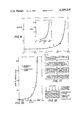
- FIG. 9 is a plot of theoretical and experimental data for spatial periodicity ratio vs. temperature ratio for laser-crystallization of a germanium film
- FIG. 10 is a plot of theoretical and experimental data for the spatial period structural features of laser-crystallized germanium films as a function of background temperature
- FIG. 11 is a block diagram which illustrates one method for fabricating a photovoltaic cell employing laser beam scanning of a semiconductor film as described herein;
- FIG. 12 is a cross-sectional view of a photovoltaic cell which could be prepared by the method illustrated in FIG. 11;
- FIG. 13 is a block diagram which illustrates an alternative method for fabricating a photovoltaic cell employing laser beam scanning of the semiconductor film as described herein;
- FIG. 14 is a cross-sectional view of a photovoltaic cell which could be prepared by the method illustrated in FIG. 13;
- FIG. 15 is a block diagram which illustrates still another alternative method for fabricating a photovoltaic cell employing laser beam scanning of a semiconductor film as described herein;
- FIG. 16 is a block diagram of a photovoltaic cell prepared by the method illustrated in FIG. 15;
- FIG. 17 is a schematic diagram illustrating crystallization according to this invention with a spatially and temporarily modulated energy beam
- FIG. 18 is a schematic diagram of an apparatus suitable for crystallizing amorphous materials according to this invention by employing an electron beam or an ion beam;
- FIG. 19 is a schematic diagram of an apparatus for crystallizing amorphous materials according to this invention employing a train of electrical pulses simulating a moving energy beam.
- Laser 10 which is a high power, high efficiency laser, such as a Nd:YAG laser, emits laser beam 12 which is focused to a spot having the shape and size desired by focusing lens 14.
- a preferred shape is one which has a large aspect ratio, such as an elongated slit, because such shapes can be used to align semiconductor crystallites as well as to enlarge them. This is apparently because the slit produces thermal gradients in the semiconductor film transverse to its long axis. Because of these temperature gradients, crystallization of the film results in a preferred alignment and growing, aligned domains then tend to coalesce as the scanning continues producing larger, more aligned grains.
- the exact size and shape of the focused laser spot will depend upon factors such as laser power, scanning rate, area to be scanned, crystalline properties desired, etc. Various shapes are obtainable by employing beam expanders, cylindrical lenses, mirrors, or other optical or mechanical elements known to those skilled in the art. For reasons of practicality, it is preferred to use a spot size having an area of at least about 10 -4 cm 2 . It is also particularly preferred, as mentioned above, to employ a laser image having a large aspect ratio. For example, if the beam is rectangular in shape, it is preferred to have the aspect ratio (l/w) greater than 10. Large aspect ratios provide uniform temperature gradients which, in turn, promote aligned crystallites.
- Beam splitter 16 is used to divide focused beam 12 so that a first portion is reflected to power detector 18 and a second portion is transmitted to electro-optical scanner 20.
- Power detector 18 serves to measure the exact beam power so that any desired changes in laser power, scanning rate, etc., can be made.
- Electro-optical scanner 20 is one convenient means for scanning focused beam 12. After passing scanner 20, focused beam 12 enters sample chamber 22 through transparent window 24 and strikes the surface of semiconductor 26.
- Scanning of semiconductor 26 can be achieved by mounting sample chamber 22 upon three translational stages, 28, 30 and 32.
- Translational stages 28, 30 and 32 provide the capability to move chamber 22, and thus semiconductor 26, in the x, y and z directions, respectively.
- Each stage can be independently driven by connecting rotatable arms 34, 36 and 38 to electric motors (not shown).
- Each stage can be driven separately, or any combination can be driven simultaneously. Also, the rate at which each stage can be driven is variable. Thus, a great variety of scan patterns and rates is achievable.
- electro-optic or acousto-optical beam deflectors or other means to raster the laser beam can also be used, and these are known to those skilled in the art.
- scanning can be achieved by moving either the sample or the beam, or both.
- the scan rate is set, of course, by the dwell time required. As a general rule, however, the scan rates used with this invention are higher than those used with prior methods.
- Radiant heating lamp 40 can be used to help heat the semiconductor 26. Induction heaters, resistance heaters, or other means to heat semiconductor 26 could, of course, also be employed.
- FIG. 1 is typical of that employed in our previous patent, U.S. Pat. No. 4,059,461.
- the teachings of our prior patent are hereby incorporated by reference, particularly in regard to other suitable apparatus for carrying out a laser-crystallization process and for matching the characteristics of the laser to the amorphous material to be scanned as well as the determination of other appropriate parameters for the method.
- Amorphous germanium (a-Ge) films were deposited by either electron-beam evaporation, rf sputtering, or ion-beam sputtering on molybdenum, graphite, or fused-silica substrates.
- the maximum temperature reached by the film during scanning estimated from its color, was about 700° C., far below the melting point of crystalline Ge, which is about 937° C. Because of this, the transformations from amorphous to crystalline described herein are referred to as "solid phase transformations". This means that the maximum temperature reached by the material as a result of the energy beam is below the melting point of the crystalline phase of the material.
- FIG. 2 shows an optical transmission micrograph of one such film, obtained with visible radiation from a xenon lamp.
- the dark areas in the micrograph are regions of untransformed a-Ge, which for the film thickness used was almost opaque to visible and near-infrared radiation, while the bright areas are regions of crystalline Ge, which had significant transmission in the red and near-infrared. Similar contrast was also obtained using infrared microscopy.
- Each periodic feature consisted of four different regions, as shown in FIG. 3. These were a narrow amorphous region, followed by another region containing a mixture of amorphous material and fine grains, and then a broad region of fine crystallites, and finally another broad region of much larger, elongated crystallites having dimensions of about 1-2 ⁇ 20 micrometers, generally aligned parallel to each other but at an angle of about 55° to the laser scan direction.
- the large crystallites within each periodic feature formed a roughly chevron-like pattern, with the two halves of the pattern symmetrical about an axis parallel to the scan direction and located near the center of the laser slit image.
- the angles between the long axes of the crystallites and the scan direction were similar in magnitude but of opposite sense for the two halves of the pattern.
- the symmetry axis lies close to or just below the bottom of the micrograph, so that only half the chevron pattern can be seen.
- FIG. 4 is a TEM bright-field micrograph of a portion of a film that was laser-scanned with T b equal to room temperature. The micrograph illustrates the same sequence of regions found by optical microscopy and shown in FIG. 2: amorphous (the dark area), amorphous-plus-crystalline, fine-grain and large-grain. The fine-grain region yields a transmission electron diffraction pattern like the one shown in FIG. 5, with the rings typical of polycrystalline material.
- the grain size gradually increases until it reaches about 0.3 ⁇ m, the thickness of the film, then increases abruptly to give the large, well-aligned crystallites of the final region, which are clearly visible as ribbon-like structures in the lower left corner of the micrograph of FIG. 4. This is the end portion of the preceeding periodic feature. It has been demonstrated by bright-field and dark-field TEM that each of these structures is a single grain, and that they yield characteristic single-crystal transmission electron diffraction patterns. FIG. 6 is an example of such a diffraction pattern.
- FIG. 7 is a schematic diagram illustrating the geometry considered.
- the film is deposited on a thick substrate that is heated to T b , and the laser image is scanned from left to right at velocity v.
- the approximation was made that the amorphous-crystalline (a-c) transformation occurs instantaneously when the film reaches a critical temperature T c .
- T c critical temperature
- the basis for this approximation is that the rate of transformation increases exponentially with temperature. See Blum, N. A. and Feldman, C., J. Non-Cryst. Solids, 22, 29 (1976). This means that over a narrow temperature interval the ratio of the time required for transformation to the time required for laser scan changes from >>1 to ⁇ 1.
- the a-c boundary therefore coincides with a T c isotherm, and the motion of the boundary can be found by calculating the motion of the isotherm.
- Crystallization of the amorphous film begins when the film temperature reaches T c along a line at the left edge of the film that is parallel to the long axis of the laser image. Because the film temperature ahead of the image is then increased by conduction of the latent heat as well as by laser heating, the T c isotherm, and therefore the a-c boundary, move to the right at a velocity v ac that is initially much higher than v. As the boundary moves away from the laser image, the contribution of laser heating to the temperature at the boundary decreases rapidly.
- T b With increasing T b , this distance increases, since less heat is required to increase the film temperature to T c , so that the a-c boundary moves farther beyond the laser image before it comes to rest. If T b exceeds T r , the continuing release of latent heat is sufficient to maintain the propagation of the T c isotherm indefinitely, resulting in self-sustaining crystallization. Such self-sustaining crystallization does not result in large, aligned crystallites.
- the semiconductor film which is deposited on a thick substrate of poor thermal conductivity, is of infinite extent in the y and z directions and so thin that its temperature is constant in the x direction.
- the laser slit image is of infinite length in the z direction and moves at a velocity v from left to right in the y direction.
- the phase boundary is located at y o , with the crystalline phase to the left (y ⁇ y o ) and the untransformed amorphous phase to the right (y>y o ).
- the laser image carries with it a steady temperature profile T 1 (y-vt).
- the temperature at the phase boundary reaches T c and the boundary begins to move toward the right, with heat being liberated at a rate per boundary unit cross-sectional area of fL ⁇ Y(t), where L is the latent heat of a-c transformation of the semiconductor, ⁇ is the semiconductor density, Y(t) is the position of the boundary at time t, and f is a factor less than 1 that accounts in an approximate way for the loss of latent heat to the substrate.
- An integral equation for Y(t) can be obtained by using the condition that the temperature at the phase boundary is T c or
- Equation (3) is not in itself sufficient to give physically acceptable solutions for the motion of the phase boundary, since it allows negative values of [S( ⁇ ')+V], which imply a motion of the phase boundary back toward the laser image, with the reconversion of crystalline material to the amorphous state, accompanied by the reabsorption of latent heat.
- Equation (3) is required that, when the numerical solution of Eq. (3) yields [S( ⁇ ')+V] ⁇ 0, this quantity is to be set equal to zero, with the phase boundary remaining stationary.
- the spatial period of the structural features of laser-crystallized Ge films was determined as a function of T b .
- each film was heated to a successively higher value of T b , the laser scanned at the same power level, and the spacing measured after crystallization. This procedure was continued until T b approached the value resulting in runaway.
- this period was assumed to be equal to the distance ⁇ Y traversed by the a-c phase boundary during each of its successive jumps, from the point where crystallization is initiated by the approaching laser to the point where the boundary comes to rest ahead of the laser.
- T b and T c are expressed in °C., room temperature is much less than T c , so that ⁇ o ⁇ at room temperature, and ⁇ Y o corresponds to ⁇ o .
- the value obtained for the front velocity, V ac is dependent upon the time interval ⁇ for numerical integration, and represents a lower limit, since smaller values of St lead to higher values of V ac .
- the values obtained from the calculation for the spatial period of the oscillations are, however, independent of ⁇ .
- Results of preliminary measurements of V ac for a 0.3 ⁇ m film of amorphous germanium indicate that the value for V ac is between 150 and 400 cm/sec. The exact V ac value will depend upon such variables as film thickness, the particular semiconductor, and the substrate material and temperature. In all cases, the front velocity, V ac , is much higher than the scan velocity.
- FIG. 10 presents the experimental and theoretical data obtained in a slightly different manner. The points shown are the experimental data whereas the computer solution of Eq. 3 is plotted as a continuous curve. From these data, it can be appreciated that larger, aligned crystallites are produced by longer spatial periods.
- the scan rate of the laser beam or other energy beam can be used itself or in conjunction with the background temperature to achieve continuous, controlled motion of the crystallization front.
- the scan rate can be much more rapid than has traditionally been employed which is possible because of the solid phase nature of the amorphous--crystalline transformation.
- the scan rate of the laser beam or other energy beam need not be continuous, but may itself be pulsed in a manner which applies a pulse of energy to the crystallization front prior to the time that the front would quench to a temperature which would result in periodic structure.
- FIG. 11 illustrates diagrammatically the fabrication of a photovoltaic cell employing the laser scanning procedure described herein
- FIG. 12 illustrates a cell produced thereby.
- the first step in this fabrication is the formation of a conductive layer 52 on a substrate 50. This could be acheived, for example, by vacuum depositing a metal layer such as copper, silver, tin, gold or other metal onto substrate 50.
- Substrate 50 need not be transparent, but certainly could be. Also, substrate 50 itself could be conducting, which satisfies the first step in this fabrication.
- a film of amorphous semiconductor 54 is deposited onto conducting layer 52 or directly onto substrate 50 if it is conducting.
- An example is a depositon of a thin film of silicon during the final step in the preparation of pure silicon by a method such as the chlorosilane process.
- the cost of the amorphous silicon film could be covered in the silicon purification step.
- Any suitable semiconductor deposition process which provided the purity required could be used, of course, since the usual crystalline perfection requirements are not present because the semiconductor film will undergo laser beam or other energy beam scanning.
- Amorphous semiconductor film 54 is then scanned with a focused laser beam from a high power laser to improve its crystalline properties. This might be acheived, for example, in the case of an amorphous silicon film by the mechanical linear sweep of the silicon sheet under a slit image from a Nd:YAG laser and/or with the slit image scanned laterally back and forth by an acousto-optic or electro-optic scanner.
- a transparent rectifying contact 56 is formed with a laser-scanned semiconductor film 54. This could be done, for example, by depositing a transparent, highly conducting tin-doped indium oxide film over a thin transparent metallic layer to form a Schottky barrier. Suitable tin-doped indium oxide films are described in Fan, J.C.C., and Bachner, F.J., J. Electro Chem. Soc., 122, 1719 (1975), the teachings of which are hereby incorporated by reference. Alternatively, a rectifying contact would be formed by laser scanning in a doping atmosphere to form a p-n junction at the surface of the laser-scanned film.
- sunlight enters the photovoltaic cell through the transparent, rectifying contact 56 and passes to the laser scanned semiconductor film 54 where a photovoltaic current is generated.
- FIG. 13 illustrates diagrammatically an alternative procedure for fabricating a photovoltaic cell employing the laser scanning procedures described herein
- FIG. 14 illustrates the cell itself.
- a transparent, conductive substrate 60 is used which can be formed by depositing on transparent support 62 a conductive layer 64.
- Transparent support 62 can be glass or transparent plastic and conductive layer 64 can be a thin layer of a conductive metal.
- a conductive layer 64 is a material which will also form a recitfying contact with a semiconductor layer subsequently deposited thereon.
- a layer of tin-doped indium oxide, as previously mentioned, would serve as a conductor and would also form a Schottky barrier with some semiconductors such as silicon.
- conductive layer 64 another layer which is capable of forming a rectifying contact with the semiconductor could be deposited on to conductive layer 64.
- conductive layer 64 another layer which is capable of forming a rectifying contact with the semiconductor could be deposited on to conductive layer 64.
- one material which is transparent, conductive and capable of forming a rectifying contact with the semiconductor layer could also be used.
- the rectifying contact required can be formed upon deposition of the semiconductor film, or alternatively, in a post treatment of the film. In fact, one suitable post treatment is the laser scanning of the semiconductor film.
- a semiconductor film 66 such as a thin film of amorphous silicon, is then deposited on top of transparent, conductive substrate 60.
- a semiconductor film 66 such as a thin film of amorphous silicon
- the semiconductor film 66 is then scanned with a focused laser beam from a high power laser to improve the film's crystalline properties.
- a conductive layer 68 such as aluminum or other metal, is formed on top of laser-scanned semiconductor film 66. As can be seen in FIG. 14, sunlight enters this photovoltaic cell through the transparent, conductive substrate 60.
- FIG. 15 illustrates diagrammatically still another alternative procedure for fabricating a photovoltaic cell employing the laser scanning procedures described herein
- FIG. 16 illustrates the cell produced thereby.
- an amorphous semiconductor layer 70 is deposited on a substrate 72 which could be a metal or heavily-doped semiconductor.
- This deposited layer 70 might comprise, for example, a p + germanium layer having a thickness between 0.1 and 500 ⁇ m and being formed from amorphous germanium doped with p-dopants to a carrier level of about 10 18 carriers/cm 3 or greater.
- the amorphous germanium layer 70 is then scanned with a high power laser beam as described herein to provide a crystalline semiconductor layer 70.
- a gallium arsenide layer 74 is applied to the germanium substrate by chemical vapor deposition or other deposition technique.
- the p layer of gallium arsenide 74 can then be diffused with n-type dopant to form a shallow homojunction therein, or a separate n + GaAs layer 76 can be deposited.
- An ohmic contact 78 is then attached, and an anti-reflection coating 80 can be deposited upon the light receiving surface of the cell.
- Shallow homojunction devices of this type are described in detail in copending application Ser. No. 22,405, filed March 21, 1979, and the teachings of this application are hereby incorporated by reference.
- amorphous germanium films Although much of the actual experimental work described herein was performed employing amorphous germanium films, similar effects were observed in gallium arsenide and silicon films. It is also believed that other semiconductors could be crystallized by the method of this invention, including, but not limited to, indium phosphide, cadmium sulfide, cadmium telluride, gallium phosphide, germanium/silicon alloy, etc. Moreover, the invention described herein can also be employed in the crystallization of amorphous materials which are not semiconductor materials. These include: inorganic oxides or nitrides such as aluminum oxide or silicon dioxide; amorphous carbon; and even amorphous metals.
- the invention is suitable with materials which are not 100 percent amorphous, including mixtures of amorphous and crystalline materials. In certain cases, the latent heat liberated upon crystallization might even cause further reaction of materials.
- laser beams from a Nd:YAG laser could be employed, as well as other energy beams.
- suitable energy beams include ion beams, electron beams, or trains of electrical pulses which simulate moving energy beams.
- the energy beam then supplies sufficient energy to heat the amorphous material above T c .
- one possible method is to scan the energy beam at a velocity as fast as the crystallization front velocity V ac in order to maintain the control of the front propagation.
- the energy beam initially has a high intensity causing initiation of crystallization and advancement of the crystallization front to a position in front of the beam.
- the beam intensity is lowered but the crystallization front advances further ahead of the beam, as in FIG. 17(b).
- the beam is advanced and almost catches the crystallization front, as shown in FIG. 17(c).
- FIG. 18 illustrates an apparatus suitable for crystallizing amorphous materials by an electron or ion beam.
- This apparatus is contained within a vacuum chamber 80.
- Gun 82 can be an electron or ion beam gun, which produces energy beam 84.
- Beam 84 is focused by focusing means 86 and caused to scan by scanning means 88.
- Sample 90 is the amorphous material to be crystallized and is supported on sample holder 92 which has resistance heater 94 therein to heat sample 90.
- gun 82 is an ion beam gum, simultaneous doping of a semiconductor is possible.
- FIG. 19 illustrates still another embodiment of apparatus suitable for carrying out the invention.
- a series of voltage sources 100, 100', 100", 100''' are employed to consecutively apply electrical pulses to conducting pad sets 102, 102', 102'', 102'''. This simulates a moving beam of energy thereby causing a crystallization front to move along amorphous material 104, if the appropriate conditions are chosen.
- the invention described herein has industrial applicability in the conversion of amorphous materials, such as semiconductor films, to crystalline materials. As described above, such crystalline semiconductor films are employed in photovoltaic devices. It also has industrial applicability in the very rapid conversion of amorphous materials other than semiconductor materials to a crystalline state.
Abstract
An improved method for crystallizing amorphous material with a moving beam of energy is disclosed. In this method, the energy beam is scanned in a manner to provide controlled, continuous motion of the crystallization front.
Description
This invention was partially supported by funds from the United States Air Force.
This is a continuation-in-part of Ser. No. 75,010, filed Sept. 13, 1979, now abandoned.
This invention is in the field of materials, and more specifically relates to the conversion of amorphous materials, including amorphous semiconductor films, to crystalline materials.
It has long been recognized that the efficiency of photovoltaic cells is lowered when the semiconductor material contains a high density of grain boundaries, which are present in polycrystalline semiconductors with small grains. Thus, the attainment of high cell efficiencies is dependent on the use of crystalline semiconductor materials which eliminate all or many of these grain boundaries, such as single crystal materials or polycrystalline materials which have large, preferentially aligned crystallines. On the other hand, the production of single crystal or large-grain polycrystalline semiconductor materials has heretofore been inordinately expensive, which has detracted from the economic competitiveness of energy produced from photovoltaic cells compared with energy from other sources, such as fossil fuel generated energy.
Because of this, much research has been directed to forming semiconductor films in an amorphous state and subsequently converting these amorphous materials to a crystalline state by rapid, inexpensive techniques. Many of these techniques have involved scanning amorphous semiconductors with a high power beam of energy, such as an electron beam or laser beam. Generally, such high power beams of energy cause localized heating and melting on the semiconductor material with subsequent cooling and crystallization as the beam advances.
An example of the use of a focused beam of electrons to recrystallize small areas on the surface layer of materials is described by Steigerwald in U.S. Pat. No. 2,968,723. In a more specific application of an electron beam, Maserjian describes the production of single-crystal germanium films on sapphire substrates by heating the substrates to an elevated temperature and subsequently employing the electron beam to melt a small zone of polycrystalline germanium film thereon which forms single crystal germanium upon cooling. The substrate is heated to minimize the energy required by the electron beam which scans at a maximum frequency of 7 cm/sec. This process is stated by the author to be analogous to zone melting of semiconductor material. See Maserjian, J., "Single-Crystal Germanium Films By Micro-Zone Melting", Solid State Electronics, 6, Pergammon Press, 1963, pp. 477-84.
A two-step process and technique employing transient laser heating and melting to produce isolated regions of larger-grain polycrystalline silicon in films of fine-grain silicon on substrates such as fused silica has been described by Laff et al. See Laff, R. A. and Hutchins, G. L., IEEE Transactions On Electron Devices, Vol. ED-21, No. 11, Nov. 1974, p. 743. Because of certain disadvantages of such a laser-melting technique, others have employed radiant heating from a hot filament ribbon to give efficient thermal coupling to an amorphous silicon film in place of laser heating. See Von Gutfeld, "Crystallization of Silicon For Solar Cell Application", IBM Technical Disclosure Bulletin, 19, No. 10, March, 1977, pp. 3955-6.
Another method for improving the crystallinity of semiconductor materials by scanning them with a focused laser beam from a high-power laser suitably matched to the optical absorption properties of the semiconductor has previously been disclosed in our prior U.S. Pat. No. 4,059,461, issued on Nov. 22, 1977. An example of the use of our patented method involves the use of a focused beam from a Nd:YAG laser which is scanned across an amorphous silicon film at a rate sufficient to allow the film to heat to a temperature at which crystallization occurs. The Nd:YAG laser has been found to be particularly desirable with silicon films because of its relatively high overall power efficiency, its high power output, and because it is well matched to the absorption characteristics of an amorphous silicon film since radiation is absorbed substantially uniformly across a thickness of about 10 μm. Large silicon crystallites are obtained after scanning, and it is even possible by out method to use a shaped laser spot, such as a slit, to provide a preferred crystalline orientation within the film. Of course, other semiconductors and other lasers can be used in our method, as long as the laser wavelength and semiconductor are suitably matched and as long as the laser beam provides sufficient energy to improve the crystalline properties of the scanned film. It is particularly noteworthy that our method does not require that the semiconductor material be heated to a temperature above the melting point of the crystalline material to achieve crystallization. It is in fact preferred to carry this method out completely as a solid phase transformation.
Although our patented method has proven to be satisfactory for the crystallization of many semiconductor films, further experimentation did produce some unusual phenomena in certain cases. These included the formation of periodic structural features on semiconductor film surfaces, pulsations of film temperature during scanning, and runaway crystallization of an entire film following first contact with a laser image. Such phenomena were initially not well understood.
The invention described herein arises out of our further investigation into the unusual phenomena which sometimes occur with the laser crystallization techniques disclosed in U.S. Pat. No. 4,059,461. These further investigations include the generation of a theoretical model which can be used to predict the unusual phenomena previously observed with some film crystallizations. Because of such investigations, we have now discovered how to provide continuous, controlled motion of the crystallization front in an amorphous material by controlling parameters such as the rate at which the laser beam or other beam of energy is moved across an amorphous material and the temperature of the substrate.
In the most general sense, our invention comprises the improvement in converting amorphous material to a more crystalline state by moving an energy beam across the material under conditions which provide continuous, controlled motion of the crystallization front. One aspect of controlling the crystallization front relates to the scanning rate of the energy beam, which in the case of this invention is typically higher for most materials than scan rates previously employed with the same materials. The crystallization efficiency of these increased scan rates is surprising particularly in view of those prior art teachings in which the beam energy was employed to heat local areas of an amorphous or polycrystalline material to a molten state. Unlike crystallizations achieved by heating the material to a temperature above the melting point of the crystalline material, the crystallizations achieved by this invention are done in the solid phase. Such solid phase transformations allow lower temperatures to be employed, are extremely rapid, and result in crystallized materials having exceptionally smooth surfaces.
Another aspect of controlling the crystallization front relates to modulation of the energy beam, and in particular, spatial and/or temporal modulation of the beam intensity. In general, any modulation is sufficient that provides a crystallization front which advances fast enough to avoid quenching and periodic structure while also avoiding crystallization front runaway.
Thus, this invention offers many advantages over prior techniques for crystallizing amorphous materials, and in general, permits the rapid, uniform, solid-phase conversion of a wide variety of amorphous material to a more crystalline state.
FIG. 1 is a schematic view of an apparatus suitable for scanning amorphous material with a laser beam as described herein;
FIG. 2 is an optical transmission micrograph of a laser-crystallized germanium film having periodic structural features;
FIG. 3 is an exploded view of a small area of the micrograph of FIG. 2;
FIG. 4 is a bright-field transmission electron micrograph of a laser-crystallized germanium film;
FIGS. 5 and 6 are transmission electron diffraction patterns for fine-grained and large-grained regions of a laser-crystallized germanium film;
FIG. 7 is a schematic diagram illustrating the crystallization of an amorphous semiconductor film by a scanned slit laser image;
FIG. 8 is a plot of normalized position of amorphous-crystalline phase boundary with respect to a laser image as a function of normalized time obtained from the theoretical model for various given parameters;
FIG. 9 is a plot of theoretical and experimental data for spatial periodicity ratio vs. temperature ratio for laser-crystallization of a germanium film;
FIG. 10 is a plot of theoretical and experimental data for the spatial period structural features of laser-crystallized germanium films as a function of background temperature;
FIG. 11 is a block diagram which illustrates one method for fabricating a photovoltaic cell employing laser beam scanning of a semiconductor film as described herein;
FIG. 12 is a cross-sectional view of a photovoltaic cell which could be prepared by the method illustrated in FIG. 11;
FIG. 13 is a block diagram which illustrates an alternative method for fabricating a photovoltaic cell employing laser beam scanning of the semiconductor film as described herein;
FIG. 14 is a cross-sectional view of a photovoltaic cell which could be prepared by the method illustrated in FIG. 13;
FIG. 15 is a block diagram which illustrates still another alternative method for fabricating a photovoltaic cell employing laser beam scanning of a semiconductor film as described herein;
FIG. 16 is a block diagram of a photovoltaic cell prepared by the method illustrated in FIG. 15;
FIG. 17 is a schematic diagram illustrating crystallization according to this invention with a spatially and temporarily modulated energy beam;
FIG. 18 is a schematic diagram of an apparatus suitable for crystallizing amorphous materials according to this invention by employing an electron beam or an ion beam; and,
FIG. 19 is a schematic diagram of an apparatus for crystallizing amorphous materials according to this invention employing a train of electrical pulses simulating a moving energy beam.
The invention will now be further described with particular reference to the Figures.
An apparatus suitable for scanning semiconductor films with a focused laser beam is illustrated in FIG. 1. Laser 10, which is a high power, high efficiency laser, such as a Nd:YAG laser, emits laser beam 12 which is focused to a spot having the shape and size desired by focusing lens 14. A preferred shape is one which has a large aspect ratio, such as an elongated slit, because such shapes can be used to align semiconductor crystallites as well as to enlarge them. This is apparently because the slit produces thermal gradients in the semiconductor film transverse to its long axis. Because of these temperature gradients, crystallization of the film results in a preferred alignment and growing, aligned domains then tend to coalesce as the scanning continues producing larger, more aligned grains.
The exact size and shape of the focused laser spot will depend upon factors such as laser power, scanning rate, area to be scanned, crystalline properties desired, etc. Various shapes are obtainable by employing beam expanders, cylindrical lenses, mirrors, or other optical or mechanical elements known to those skilled in the art. For reasons of practicality, it is preferred to use a spot size having an area of at least about 10-4 cm2. It is also particularly preferred, as mentioned above, to employ a laser image having a large aspect ratio. For example, if the beam is rectangular in shape, it is preferred to have the aspect ratio (l/w) greater than 10. Large aspect ratios provide uniform temperature gradients which, in turn, promote aligned crystallites.
Scanning of semiconductor 26 can be achieved by mounting sample chamber 22 upon three translational stages, 28, 30 and 32. Translational stages 28, 30 and 32 provide the capability to move chamber 22, and thus semiconductor 26, in the x, y and z directions, respectively. Each stage can be independently driven by connecting rotatable arms 34, 36 and 38 to electric motors (not shown). Each stage can be driven separately, or any combination can be driven simultaneously. Also, the rate at which each stage can be driven is variable. Thus, a great variety of scan patterns and rates is achievable.
Of course, electro-optic or acousto-optical beam deflectors or other means to raster the laser beam can also be used, and these are known to those skilled in the art. In fact, scanning can be achieved by moving either the sample or the beam, or both.
The scan rate is set, of course, by the dwell time required. As a general rule, however, the scan rates used with this invention are higher than those used with prior methods.
The apparatus illustrated in FIG. 1 is typical of that employed in our previous patent, U.S. Pat. No. 4,059,461. The teachings of our prior patent are hereby incorporated by reference, particularly in regard to other suitable apparatus for carrying out a laser-crystallization process and for matching the characteristics of the laser to the amorphous material to be scanned as well as the determination of other appropriate parameters for the method.
To investigate some of the unusual phenomena sometimes observed in laser crystallizations, a crystallization system utilizing a cw Nd:YAG laser beam focused to a slit image with power density that is uniform to ±3% over a central area about 50 μm by 1.5 mm was employed. The samples were placed in an Ar/H2 atmosphere on a resistively-heated platform that permitted them to be scanned at various rates obtained by using synchronous motors, under the laser beam in the focal plane and normal to the long axis of the slit image. This apparatus is described in more detail in the following references, the teachings of which are hereby incorporated by reference: J. C. C. Fan, H. J. Zeiger, and P. M. Zavracky, Proc. Nat. Workshop on Low Cost Polychrystalline Silicon Solar Cells, Dallas, 1976, edited by T. L. Chu and S. S. Chu (Southern Methodist University, Dallas, 1976), p. 89; and J. C. C. Fan, J. P. Donnelly, C. O. Bozler, and R. L. Chapman, Proc. 7th Int. Symp. on GaAs and Related Compounds, St. Louis, 1978, Institute of Phys. Conf. Ser. No. 45, Chapter 6, p. 472 (1979). Amorphous germanium (a-Ge) films were deposited by either electron-beam evaporation, rf sputtering, or ion-beam sputtering on molybdenum, graphite, or fused-silica substrates.
In initial experiments on a-Ge films 2-4 micrometers thick on molybdenum and graphite substrates, the platform was heated to maintain the temperature of the film before laser irradiation (Tb) at 400°-500° C. Once crystallization was initiated by momentary irradiation at a single point, the transformation was found to be self-sustaining, with the crystallization front rapidly propagating radially outward from the irradiated spot. Films as large as 2.5 cm×2.5 cm were entirely crystallized in this manner. At lower values of Tb self-sustaining crystallization did not occur, but laser scanning yielded areas of elongated, well-aligned grains. The surface of the scanned films remained smooth, regardless of Tb. The maximum temperature reached by the film during scanning, estimated from its color, was about 700° C., far below the melting point of crystalline Ge, which is about 937° C. Because of this, the transformations from amorphous to crystalline described herein are referred to as "solid phase transformations". This means that the maximum temperature reached by the material as a result of the energy beam is below the melting point of the crystalline phase of the material.
A series of laser scanning experiments on films about 0.3 μm thick deposited by electron-beam evaporation on 1-mm thick fused silica substrates was then performed. The power density of the central area of the laser image was kept at about 5 kW/cm2, and the scan rate at 0.5 cm/sec. The background temperature Tb, which was found to be critical in crystallization behavior, was varied from room temperature to 500° C. For Tb equal to room temperature, after laser scanning, the films exhibited periodic structural features. Within each film the spatial period initially increased, but after several periods, it reached a steady-state value of about 50 μm. FIG. 2 shows an optical transmission micrograph of one such film, obtained with visible radiation from a xenon lamp. The dark areas in the micrograph are regions of untransformed a-Ge, which for the film thickness used was almost opaque to visible and near-infrared radiation, while the bright areas are regions of crystalline Ge, which had significant transmission in the red and near-infrared. Similar contrast was also obtained using infrared microscopy. Each periodic feature consisted of four different regions, as shown in FIG. 3. These were a narrow amorphous region, followed by another region containing a mixture of amorphous material and fine grains, and then a broad region of fine crystallites, and finally another broad region of much larger, elongated crystallites having dimensions of about 1-2×20 micrometers, generally aligned parallel to each other but at an angle of about 55° to the laser scan direction. In the films examined in detail, it was noted that the large crystallites within each periodic feature formed a roughly chevron-like pattern, with the two halves of the pattern symmetrical about an axis parallel to the scan direction and located near the center of the laser slit image. Thus, the angles between the long axes of the crystallites and the scan direction were similar in magnitude but of opposite sense for the two halves of the pattern. In the micrograph of FIG. 2, the symmetry axis lies close to or just below the bottom of the micrograph, so that only half the chevron pattern can be seen.
The optical microscopy results were confirmed by transmission electron microscopy (TEM) using 125 keV electrons. The TEM samples were removed from their substrates using hydrofluoric acid to partially dissolve the fused silica. FIG. 4 is a TEM bright-field micrograph of a portion of a film that was laser-scanned with Tb equal to room temperature. The micrograph illustrates the same sequence of regions found by optical microscopy and shown in FIG. 2: amorphous (the dark area), amorphous-plus-crystalline, fine-grain and large-grain. The fine-grain region yields a transmission electron diffraction pattern like the one shown in FIG. 5, with the rings typical of polycrystalline material. Within this region, the grain size gradually increases until it reaches about 0.3 μm, the thickness of the film, then increases abruptly to give the large, well-aligned crystallites of the final region, which are clearly visible as ribbon-like structures in the lower left corner of the micrograph of FIG. 4. This is the end portion of the preceeding periodic feature. It has been demonstrated by bright-field and dark-field TEM that each of these structures is a single grain, and that they yield characteristic single-crystal transmission electron diffraction patterns. FIG. 6 is an example of such a diffraction pattern. This pattern indicates that the crystallites are oriented with the normal to the plane of the substrate in a <110> direction, their long axis in a <001> direction, and a <112> direction parallel to the long axis of the laser slit image. These orientations are clearly characteristic of the solidphase growth process described herein. Since they are the same for the large crystallites throughout the film, even though these crystallites in successive periodic features are separated by regions of amorphous and randomly oriented, fine-grain material. The above experiments were repeated using values of background temperature Tb that were above room temperature but not high enough to result in self-sustaining crystallization, and the resulting scanned films exhibited periodic structural features similar to those described above.
In an effort to explain the periodic structural features formed as a result of laser scanning, the dependence of the spatial period on Tb, and the occurrence of self-sustaining crystallization at values of Tb greater than the runaway temperature Tr, a theoretical model for the dynamics of the scanned laser crystallization of an amorphous film was developed. Although the following discussion is set forth in terms of a specific system, i.e., laser scanning an amorphous semiconductor film, it should be recognized that the mathematical model produced applies very generally to other systems, and specifically to moving energy beams other than lasers and amorphous materials other than semiconductor films.
FIG. 7 is a schematic diagram illustrating the geometry considered. The film is deposited on a thick substrate that is heated to Tb, and the laser image is scanned from left to right at velocity v. The approximation was made that the amorphous-crystalline (a-c) transformation occurs instantaneously when the film reaches a critical temperature Tc. The basis for this approximation is that the rate of transformation increases exponentially with temperature. See Blum, N. A. and Feldman, C., J. Non-Cryst. Solids, 22, 29 (1976). This means that over a narrow temperature interval the ratio of the time required for transformation to the time required for laser scan changes from >>1 to <<1. The a-c boundary therefore coincides with a Tc isotherm, and the motion of the boundary can be found by calculating the motion of the isotherm.
Crystallization of the amorphous film, accompanied by liberation of latent heat, begins when the film temperature reaches Tc along a line at the left edge of the film that is parallel to the long axis of the laser image. Because the film temperature ahead of the image is then increased by conduction of the latent heat as well as by laser heating, the Tc isotherm, and therefore the a-c boundary, move to the right at a velocity vac that is initially much higher than v. As the boundary moves away from the laser image, the contribution of laser heating to the temperature at the boundary decreases rapidly. The continuing liberation of latent heat tends to maintain the forward motion of the boundary, but if Tb is less than Tr, heat conduction within the film eventually reduces the boundary temperature below Tc, and the boundary abruptly stops moving. At this time, there is a region of crystallized material between the laser image and the left edge of the untransformed film. The boundary then remains at rest until its temperature is increased to Tc by the approaching laser image, and the whole process is repeated. Thus, although the laser image is scanned at a constant velocity, the a-c boundary moves in a series of rapid jumps between rest positions. According to the model, the periodic structural features of the laser-scanned film are due to this periodic motion of the boundary, and the spatial period of these features is the distance between successive rest positions. With increasing Tb, this distance increases, since less heat is required to increase the film temperature to Tc, so that the a-c boundary moves farther beyond the laser image before it comes to rest. If Tb exceeds Tr, the continuing release of latent heat is sufficient to maintain the propagation of the Tc isotherm indefinitely, resulting in self-sustaining crystallization. Such self-sustaining crystallization does not result in large, aligned crystallites.
The actual derivation of the theoretical model will now be given.
The semiconductor film, which is deposited on a thick substrate of poor thermal conductivity, is of infinite extent in the y and z directions and so thin that its temperature is constant in the x direction. The laser slit image is of infinite length in the z direction and moves at a velocity v from left to right in the y direction. At t=0, the phase boundary is located at yo, with the crystalline phase to the left (y<yo) and the untransformed amorphous phase to the right (y>yo). The laser image carries with it a steady temperature profile T1 (y-vt). At t=0, the temperature at the phase boundary reaches Tc and the boundary begins to move toward the right, with heat being liberated at a rate per boundary unit cross-sectional area of fLρY(t), where L is the latent heat of a-c transformation of the semiconductor, ρ is the semiconductor density, Y(t) is the position of the boundary at time t, and f is a factor less than 1 that accounts in an approximate way for the loss of latent heat to the substrate. Then the temperature T(y,t) at any point y along the film at time t is given by the one-dimensional integral relation ##EQU1## where C is the specific heat of the film, κ=K/Cρ defines its thermal diffusivity, and K is its thermal conductivity. An integral equation for Y(t) can be obtained by using the condition that the temperature at the phase boundary is Tc or
T[Y(t),t]=T.sub.c (2)
For purposes of calculation, it is convenient to rewrite Eq. (2) in the frame of reference moving with the laser image. For this purpose, the position variable u(t)=y(t)-vt is introduced, where u(t) is measured from the center of the laser image as origin. The temperature T1 is modeled in the form T1 (u)=Tb +ΔTl exp[-(u/a2)], where Tb is a uniform, time-independent background temperature and the temperature contribution due to the laser is described by a Gaussian of width a and magnitude ΔTl. Finally, introducing normalized quantities, the integral equation for the motion of the phase boundary can be written as ##EQU2## where
α=ΔT.sub.l /(T.sub.c -T.sub.b) (4a)
η=fL/Cπ.sup.1/2 (T.sub.c -T.sub.b) (4b)
τ.tbd.4κt/a.sup.2, V.tbd.av/4κ, S.tbd.U/a, S(τ').tbd.[dS(τ')/dτ']=(1/a)[dU(τ')/dt')]dt'/dτ', and U is the position of the phase boundary measured from the center of the laser image.
Equation (3) is not in itself sufficient to give physically acceptable solutions for the motion of the phase boundary, since it allows negative values of [S(γ')+V], which imply a motion of the phase boundary back toward the laser image, with the reconversion of crystalline material to the amorphous state, accompanied by the reabsorption of latent heat. To constrain Eq. (3) to physically acceptable solutions it is required that, when the numerical solution of Eq. (3) yields [S(τ')+V]≦0, this quantity is to be set equal to zero, with the phase boundary remaining stationary.
Equation (3) has been solved numerically to obtain S as a function of τ for representative values of α, η, and V, with the boundary conditions that S(τ)=0 t τ=0 and that S(0) is given by 1=αexp {-[S(0)2 ]}. The inset of FIG. 8 calculated for α=3.6, η=0.6, and V=0.3, depicts the approach to the steady state oscillatory type of solution characteristic of Eq. (3). FIG. 8 shows plots of S vs τ for V=0.3 and three increasing values of η, with α increasing in proportion to η (which corresponds, from Eqs. (4a) and (4b), to increasing Tb toward Tc while holding ΔTl fixed). For each value of η, S initially increases rapidly because the latent heat liberated by the phase transformation raises the temperature ahead of the boundary, accelerating its forward motion. As the boundary moves away from the laser image, the contribution of the laser to the temperature ahead of the boundary decreases rapidly. For η=0.3 the boundary motion soon decelerates, and the boundary comes to rest, remaining fixed for a time interval during which its temperature initially drops rapidly below Tc and S decreases with velocity S=-V. With the approach of the laser image, the boundary temperature gradually increases to Tc, the boundary once more moves forward, and S again increases. This cycle is repeated indefinitely, resulting in the oscillations in S seen for η=0.3 in FIG. 8.
When η is increased by increasing Tb, less latent heat is required to heat the film to Tc ahead of the laser image, and the phase boundary moves farther beyond the laser before it decelerates and comes to rest. This trend is illustrated by the calculated curve for η=0.6 in FIG. 8, and leads to periodic motion with a longer period. When η becomes large enough, the heat liberated during crystallization is sufficient to sustain the transformation, causing the boundary to "run away" from the laser image. This situation, which is illustrated by the curve for η=0.8 in FIG. 8, accounts for the observation that the entire film is crystallized following momentary contact with the laser image.
For the three curves shown in FIG. 8, the average value of S(τ) during each of the times when the phase boundary is moving ahead of the laser image is seen to be approximately the same and essentially independent of η.
In addition to explaining runaway crystallization, the proposed model can also explain other qualitative observations on laser crystallization. For example, different regions of such films can be expected to differ in microstructure depending on their rates of transformation and therefore on their thermal history. This suggests that the periodic structural features observed on laser-crystallized films, such as that seen in FIG. 2, can be attributed to oscillations in S like those implied by the curves for η=0.3 and 0.6 in FIG. 8. Furthermore, for sufficiently high values of η these oscillations produce large fluctuations in the rate of heat liberation and therefore in temperature. This can explain the periodic fluctuations in color temperature observed during some laser crystallization experiments.
In order to carry out a semi-quantitative test of the model, the spatial period of the structural features of laser-crystallized Ge films was determined as a function of Tb. Experiments were performed on amorphous films 0.3 μm thick, deposited on fused silica substrates and scanned at v=0.5 cm/sec with the slit image of a cw Nd:YAG laser. Initially, a film at room temperature was irradiated at a laser power level just high enough to produce crystallization, which yielded structure in the transformed film with a spatial period of ˜50 μm. In the following experiments each film was heated to a successively higher value of Tb, the laser scanned at the same power level, and the spacing measured after crystallization. This procedure was continued until Tb approached the value resulting in runaway.
To use the model to calculate the spatial period in the film, it was assumed that this period was equal to the distance ΔY traversed by the a-c phase boundary during each of its successive jumps, from the point where crystallization is initiated by the approaching laser to the point where the boundary comes to rest ahead of the laser. This distance is just equal to (aVΔτ), where V is the normalized laser scanning velocity and Δτ is the normalized time interval between the beginnings of two successive jumps, i.e., the period of the oscillations in S illustrated by the curves for η=0.3 and 0.6 in FIG. 8.
To obtain a relationship between ΔY and Tb, Eq. (3) was first used to calculate VΔτ as a function of η for representative values of α and V. The calculated curve for α=6η (corresponding to fixed ΔTl) and V=0.3 is shown in the inset of FIG. 9. With increasing η, Δτ and therefore VΔτ increase rapidly, leading to boundary runaway by η=0.65. For a given value of η, VΔτ was found to be quite insensitive to either α or V, showing that the boundary jump distance is determined primarily by the properties of the film and by Tb, and does not depend strongly on either the power or velocity of the laser.
In order to compare theory with experiment, the curve of VΔτ vs η shown in the inset of FIG. 9 was used to obtain curves relating the ratios ΔY/ΔYo and Tb /Tc, where ΔYo is the spatial period in the film (i.e., the boundary jump distance) for Tb of room temperature. To calculate these curves, Eq. (4b) was rewritten in the lumped-parameter form η=ηo /(1-Tb /Tc), where ηo .tbd.fL/π1/2 CTc. If Tb and Tc are expressed in °C., room temperature is much less than Tc, so that ηo ≈η at room temperature, and ΔYo corresponds to ηo. Curves of ΔY/ΔYo vs Tb /Tc =1-ηo /η were calculated by adopting pairs of numerical values of ηo and Tc, then compared with the experimental points (for each point, the adopted value of Tc was used to determine Tb /Tc). A reasonable overall fit has been obtained, as shown in FIG. 9, for ηo =0.14 and Tc =685° C. The abrupt increase in ΔY/ΔYo when Tb /Tc exceeds about 0.7 is associated with the approach of Tb to the value Tr above which laser irradiation results in boundary runaway. From the calculations, Tr is about 0.775 Tc =530° C.
From the definition of ηo, fL=π1/2 CTc ηo. Taking C=0.08 cal/g°C. for amorphous Ge and the values of Tc and ηo used for FIG. 9, fL=13.6 cal/g. In calorimetric measurements made during the rapid heating of amorphous Ge films, Chen and Turnbull observed a sharp transistion at ˜500° C. and measured L=37.1 cal/g. See H. S. Chen and D. Turnbull, J. Appl. Phys., 40, 4214 (1969). Using the model result for fL gave a value of only about 1/3 for f.
The Gaussian width of the laser temperature profile can be determined from the relationship a=ΔY/VΔτ. From the measured ΔYo =50 μm at room temperature and VΔτ.tbd.0.25 correspondong to ηo in the inset of FIG. 9, a˜200 μm. The phase boundary velocity vac can then be determined from the normalized boundary velocity Vac ˜1.9 by using the relation vac =4κVac /a. For κ=KρC, a value of 0.09 cm2 /sec is estimated by taking K=0.035 cal/cm sec°C., ρ≈5 g/cm3, and C=0.08 cal/g°C. The valued obtained for Vac is then ˜ 35 cm/sec, much higher than the laser scan velocity v=0.5 cm/sec.
The value obtained for the front velocity, Vac, is dependent upon the time interval δτ for numerical integration, and represents a lower limit, since smaller values of St lead to higher values of Vac. The values obtained from the calculation for the spatial period of the oscillations are, however, independent of δτ. Results of preliminary measurements of Vac for a 0.3 μm film of amorphous germanium indicate that the value for Vac is between 150 and 400 cm/sec. The exact Vac value will depend upon such variables as film thickness, the particular semiconductor, and the substrate material and temperature. In all cases, the front velocity, Vac, is much higher than the scan velocity.
FIG. 10 presents the experimental and theoretical data obtained in a slightly different manner. The points shown are the experimental data whereas the computer solution of Eq. 3 is plotted as a continuous curve. From these data, it can be appreciated that larger, aligned crystallites are produced by longer spatial periods.
From the above, it can be seen that the scan rate of the laser beam or other energy beam, can be used itself or in conjunction with the background temperature to achieve continuous, controlled motion of the crystallization front. The scan rate can be much more rapid than has traditionally been employed which is possible because of the solid phase nature of the amorphous--crystalline transformation. Of course, the scan rate of the laser beam or other energy beam need not be continuous, but may itself be pulsed in a manner which applies a pulse of energy to the crystallization front prior to the time that the front would quench to a temperature which would result in periodic structure.
FIG. 11 illustrates diagrammatically the fabrication of a photovoltaic cell employing the laser scanning procedure described herein, and FIG. 12 illustrates a cell produced thereby. The first step in this fabrication is the formation of a conductive layer 52 on a substrate 50. This could be acheived, for example, by vacuum depositing a metal layer such as copper, silver, tin, gold or other metal onto substrate 50. Substrate 50 need not be transparent, but certainly could be. Also, substrate 50 itself could be conducting, which satisfies the first step in this fabrication.
Then, a film of amorphous semiconductor 54 is deposited onto conducting layer 52 or directly onto substrate 50 if it is conducting. An example is a depositon of a thin film of silicon during the final step in the preparation of pure silicon by a method such as the chlorosilane process. Thus, the cost of the amorphous silicon film could be covered in the silicon purification step. Any suitable semiconductor deposition process which provided the purity required could be used, of course, since the usual crystalline perfection requirements are not present because the semiconductor film will undergo laser beam or other energy beam scanning.
Finally, a transparent rectifying contact 56 is formed with a laser-scanned semiconductor film 54. This could be done, for example, by depositing a transparent, highly conducting tin-doped indium oxide film over a thin transparent metallic layer to form a Schottky barrier. Suitable tin-doped indium oxide films are described in Fan, J.C.C., and Bachner, F.J., J. Electro Chem. Soc., 122, 1719 (1975), the teachings of which are hereby incorporated by reference. Alternatively, a rectifying contact would be formed by laser scanning in a doping atmosphere to form a p-n junction at the surface of the laser-scanned film.
As illustrated in FIG. 12, sunlight enters the photovoltaic cell through the transparent, rectifying contact 56 and passes to the laser scanned semiconductor film 54 where a photovoltaic current is generated.
FIG. 13 illustrates diagrammatically an alternative procedure for fabricating a photovoltaic cell employing the laser scanning procedures described herein, and FIG. 14 illustrates the cell itself. In this fabrication procedure, a transparent, conductive substrate 60 is used which can be formed by depositing on transparent support 62 a conductive layer 64. Transparent support 62 can be glass or transparent plastic and conductive layer 64 can be a thin layer of a conductive metal. Prefereably, a conductive layer 64 is a material which will also form a recitfying contact with a semiconductor layer subsequently deposited thereon. A layer of tin-doped indium oxide, as previously mentioned, would serve as a conductor and would also form a Schottky barrier with some semiconductors such as silicon. Alternatively, another layer which is capable of forming a rectifying contact with the semiconductor could be deposited on to conductive layer 64. Of course, one material which is transparent, conductive and capable of forming a rectifying contact with the semiconductor layer could also be used. Also, the rectifying contact required can be formed upon deposition of the semiconductor film, or alternatively, in a post treatment of the film. In fact, one suitable post treatment is the laser scanning of the semiconductor film.
A semiconductor film 66, such as a thin film of amorphous silicon, is then deposited on top of transparent, conductive substrate 60. As noted previously, many of the known processes for depositing semiconductor films can be used since the usual limitations on crystal perfection are obviated with subsequent laser scanning of the film.
The semiconductor film 66 is then scanned with a focused laser beam from a high power laser to improve the film's crystalline properties. Lastly, a conductive layer 68, such as aluminum or other metal, is formed on top of laser-scanned semiconductor film 66. As can be seen in FIG. 14, sunlight enters this photovoltaic cell through the transparent, conductive substrate 60.
FIG. 15 illustrates diagrammatically still another alternative procedure for fabricating a photovoltaic cell employing the laser scanning procedures described herein, and FIG. 16 illustrates the cell produced thereby. In this procedure, an amorphous semiconductor layer 70 is deposited on a substrate 72 which could be a metal or heavily-doped semiconductor. This deposited layer 70 might comprise, for example, a p+ germanium layer having a thickness between 0.1 and 500 μm and being formed from amorphous germanium doped with p-dopants to a carrier level of about 1018 carriers/cm3 or greater. The amorphous germanium layer 70 is then scanned with a high power laser beam as described herein to provide a crystalline semiconductor layer 70. Subsequently, a gallium arsenide layer 74 is applied to the germanium substrate by chemical vapor deposition or other deposition technique. The p layer of gallium arsenide 74 can then be diffused with n-type dopant to form a shallow homojunction therein, or a separate n+ GaAs layer 76 can be deposited. An ohmic contact 78 is then attached, and an anti-reflection coating 80 can be deposited upon the light receiving surface of the cell. Shallow homojunction devices of this type are described in detail in copending application Ser. No. 22,405, filed March 21, 1979, and the teachings of this application are hereby incorporated by reference.
Although much of the actual experimental work described herein was performed employing amorphous germanium films, similar effects were observed in gallium arsenide and silicon films. It is also believed that other semiconductors could be crystallized by the method of this invention, including, but not limited to, indium phosphide, cadmium sulfide, cadmium telluride, gallium phosphide, germanium/silicon alloy, etc. Moreover, the invention described herein can also be employed in the crystallization of amorphous materials which are not semiconductor materials. These include: inorganic oxides or nitrides such as aluminum oxide or silicon dioxide; amorphous carbon; and even amorphous metals.
It should also be recognized that the invention is suitable with materials which are not 100 percent amorphous, including mixtures of amorphous and crystalline materials. In certain cases, the latent heat liberated upon crystallization might even cause further reaction of materials.
Similarly, although the work described above was performed with laser beams from a Nd:YAG laser, other lasers could be employed, as well as other energy beams. Examples of other suitable energy beams include ion beams, electron beams, or trains of electrical pulses which simulate moving energy beams.
Often, it is desirable to heat the substrate to an elevated temperature, but this must always be below Tc. The energy beam then supplies sufficient energy to heat the amorphous material above Tc. In addition, one possible method is to scan the energy beam at a velocity as fast as the crystallization front velocity Vac in order to maintain the control of the front propagation.
In certain cases, it would be advantageous to modulate the rapidly scanning beam to maintain even better control of the front propagation. In some of these cases; it is preferable to employ a spatially and temporally modulated beam, as is schematically illustrated in FIG. 17. As illustrated in FIG. 17(a), the energy beam initially has a high intensity causing initiation of crystallization and advancement of the crystallization front to a position in front of the beam. At a later time, the beam intensity is lowered but the crystallization front advances further ahead of the beam, as in FIG. 17(b). At a still later time and before the film quenches to cause periodic structure, the beam is advanced and almost catches the crystallization front, as shown in FIG. 17(c). In FIG. 17(d), the laser intensity is increased and the crystallization front again moves away from the beam. In FIG. 17(e), the laser intensity is decreased, but before quenching can occur, the beam is moved towards the front, as in FIG. 17(f). Such spatial and temporal modulation is continued, as shown in FIG. 17(g)-FIG. 17(k), until the desired crystallization has been completed. In this manner, the quenching of the film to a temperature below Tc is avoided at one extreme whereas runaway crystallization is avoided at the other extreme.
FIG. 18 illustrates an apparatus suitable for crystallizing amorphous materials by an electron or ion beam. This apparatus is contained within a vacuum chamber 80. Gun 82 can be an electron or ion beam gun, which produces energy beam 84. Beam 84 is focused by focusing means 86 and caused to scan by scanning means 88. Sample 90 is the amorphous material to be crystallized and is supported on sample holder 92 which has resistance heater 94 therein to heat sample 90. In the case where gun 82 is an ion beam gum, simultaneous doping of a semiconductor is possible.
FIG. 19 illustrates still another embodiment of apparatus suitable for carrying out the invention. In this apparatus, a series of voltage sources 100, 100', 100", 100''' are employed to consecutively apply electrical pulses to conducting pad sets 102, 102', 102'', 102'''. This simulates a moving beam of energy thereby causing a crystallization front to move along amorphous material 104, if the appropriate conditions are chosen.
The invention described herein has industrial applicability in the conversion of amorphous materials, such as semiconductor films, to crystalline materials. As described above, such crystalline semiconductor films are employed in photovoltaic devices. It also has industrial applicability in the very rapid conversion of amorphous materials other than semiconductor materials to a crystalline state.
There are many equivalents to the embodiments specifically described herein and such equivalents are intended to be covered by the following claims. For example, although amorphous films or amorphous layers are referred to in many instances, films and layers are meant to be interchangeable.
Claims (34)
1. A method of converting solid amorphous material to a more crystalline state comprising the steps of:
(a) heating a portion of said material with energy from an energy beam to bring such portion to its crystallization temperature while maintaining the temperature below the melting temperature of the crystalline state of the material; and
(b) moving said energy beam in relation to said material at a velocity V, which is less than or equal to Vac but fast enough to provide continuous controlled motion of the crystallization front; wherein Vac is the normalized boundary velocity of the transformation of the amorphous material to crystalline.
2. The method of claim 1 wherein said material comprises a semiconductor film.
3. The method of claim 2 wherein said energy beam is a laser beam, electron beam, ion beam, train of electrical pulses, or a combination thereof.
4. The method of claim 3 wherein said beam is shaped to a focused image having a large aspect ratio.
5. The method of claim 2 wherein said energy beam comprises a focused, shaped laser beam.
6. The method of claim 5 wherein said laser beam has an aspect ratio of greater than about 10.
7. The method of claim 6 wherein said semiconductor film comprises a germanium film and the laser beam employed originates from a continuous wave Nd:YAG laser.
8. The method of claim 5 wherein said laser beam is modulated spatially and temporally.
9. The method of claim 8 wherein said laser beam is focused to a slit image.
10. The method of claim 2 wherein said film is preheated with a source of heat other than said laser beam.
11. The method of claim 10 wherein said semiconductor film is supported on a substrate.
12. In the method of crystallizing an amorphous material by scanning it with an energy beam:
providing continuous controlled motion of the crystallization front by (a) maintaining the background temperature of the amorphous material at a value which is between the temperature at which periodic structure occurs and the temperature which produces runaway crystallization and (b) modulating the beam and scanning a surface of the material with the beam at a rate less than or equal to the normalized boundary velocity of the crystallization front.
13. The improvement of claim 12 wherein said energy beam is a laser beam.
14. A method for producing a crystalline semiconductor film, comprising:
a. forming an amorphous film of a semiconductor on a substrate; and,
b. scanning said amorphous film to crystallize it with a laser beam, said laser beam being modulated to provide continuous, controlled motion of the crystallization front, the scanning rate being less than or equal to the velocity of the crystallization front and the modulation of the laser beam being at an energy level to crystallize the material without achieving a temperature equal to or greater than the crystalline melting point of the material.
15. A method of claim 14 wherein said laser is a Nd:YAG laser.
16. A method of claim 15 wherein said amorphous film comprises an amorphous silicon film.
17. A method of claim 15 wherein said amorphous film comprises an amorphous germanium film.
18. A method of claim 15 wherein said amorphous film comprises an amorphous germanium/silicon alloy film.
19. A method of claim 15 wherein said amorphous film comprises an amorphous gallium arsenide film.
20. A method of crystallizing an amorphous inorganic material in the solid phase comprising scanning said material with an energy beam sufficient to provide continuous, controlled motion of the crystallization front velocity but insufficient energy to reach the melting point of the crystalline material; the scanning rate being less than or equal to the crystallization front velocity.
21. A method of claim 20 wherein said inorganic material comprises aluminum oxide.
22. A method of claim 20 wherein said inorganic material comprises silicon dioxide.
23. A method of fabricating a photovoltaic cell, comprising:
a. forming a conductive layer on a substrate;
b. forming an amorphous semiconductor film on said conductive layer;
c. scanning said amorphous semiconductor film with an energy beam at a rate which is less than or equal to the crystallization wavefront velocity and at an energy level high enough to provide continuous, controlled motion of the crystallization front to improve the crystallinity of said semiconductor film but below the melting temperature of the crystalline state of the film; and,
d. forming a transparent rectifying contact with the scanned film.
24. A method of claim 23 wherein said beam comprises a laser beam.
25. A method of fabricated a photovoltaic cell, comprising:
a. forming an amorphous semiconductor film on a transparent, conductive substrate;
b. forming a rectifying contact between the amorphous semiconductor film and substrate;
c. scanning said amorphous semiconductor film with an energy beam at a rate which is less than or equal to the crystallization wavefront velocity but at an energy level low enough to prevent reaching the crystalline melting point of the film to provide continuous, controlled motion of the crystallization front to improve the crystallinity of said semiconductor film; and,
d. forming a conductive layer on the scanned film.
26. A method of claim 25 wherein said beam comprises a laser beam.
27. A method of fabricating a photovoltaic cell, comprising:
a. depositing an amorphous semiconductor layer;
b. scanning said amorphous semiconductor layer with an energy beam at a rate which is less than or equal to the crystallization wavefront velocity and at an energy level low enough to avoid the crystalline melting point of the layer thereby to provide a continuous, controlled motion of a crystallization front to form a crystalline semiconductor substrate;
c. forming an active semiconductor film on said substrate;
d. forming a p-n junction in said active film; and,
e. forming an ohmic contact to said active semiconductor film.
28. A method of claim 27 wherein said amorphous semiconductor layer comprises germanium.
29. A method of claim 28 wherein said active semiconductor layer comprises gallium arsenide.
30. A method of claim 29 wherein said p-n junction comprises a shallow homojunction.
31. A method of claim 30 including the additional step of applying an antireflection coating over said active semiconductor layer.
32. In the fabrication of a shallow homojunction solar cell from a semiconductor layer:
The improvement wherein said layer is formed from an amorphous semiconductor layer scanned with an energy beam at a rate which is less than or equal to the crystallization wavefront velocity and at an energy level low enough to prevent the temperature of the layer to reach its crystalline melting point thereby to provide continuous, controlled motion of the crystallization front to form a crystalline semiconductor layer for said shallow homojunction solar cell.
33. The improvement of claim 32 wherein said amorphous substrate comprises germanium.
34. In the method of crystallizing an amorphous material with a moving energy beam:
The improvement of modulating said energy beam in conjunction with heating said material to an elevated temperature at a rate which is less than or equal to the crystallization wavefront velocity and at an energy level low enough to prevent liquifying or vaporizing the material thereby to provide a controlled, continuous crystallization front.
Priority Applications (5)
| Application Number | Priority Date | Filing Date | Title |
|---|---|---|---|
| US06/123,745 US4309225A (en) | 1979-09-13 | 1980-02-22 | Method of crystallizing amorphous material with a moving energy beam |
| PCT/US1980/001151 WO1981000789A1 (en) | 1979-09-13 | 1980-09-08 | Improved method of crystallizing amorphous material with a moving energy beam |
| JP50226780A JPS56501508A (en) | 1979-09-13 | 1980-09-08 | |
| DE8080901915T DE3072022D1 (en) | 1979-09-13 | 1980-09-08 | Improved method of crystallizing amorphous material with a moving energy beam |
| EP80901915A EP0035561B1 (en) | 1979-09-13 | 1981-03-23 | Improved method of crystallizing amorphous material with a moving energy beam |
Applications Claiming Priority (2)
| Application Number | Priority Date | Filing Date | Title |
|---|---|---|---|
| US7501079A | 1979-09-13 | 1979-09-13 | |
| US06/123,745 US4309225A (en) | 1979-09-13 | 1980-02-22 | Method of crystallizing amorphous material with a moving energy beam |
Related Parent Applications (1)
| Application Number | Title | Priority Date | Filing Date |
|---|---|---|---|
| US7501079A Continuation-In-Part | 1979-09-13 | 1979-09-13 |
Publications (1)
| Publication Number | Publication Date |
|---|---|
| US4309225A true US4309225A (en) | 1982-01-05 |
Family
ID=26756323
Family Applications (1)
| Application Number | Title | Priority Date | Filing Date |
|---|---|---|---|
| US06/123,745 Expired - Lifetime US4309225A (en) | 1979-09-13 | 1980-02-22 | Method of crystallizing amorphous material with a moving energy beam |
Country Status (5)
| Country | Link |
|---|---|
| US (1) | US4309225A (en) |
| EP (1) | EP0035561B1 (en) |
| JP (1) | JPS56501508A (en) |
| DE (1) | DE3072022D1 (en) |
| WO (1) | WO1981000789A1 (en) |
Cited By (157)
| Publication number | Priority date | Publication date | Assignee | Title |
|---|---|---|---|---|
| US4385937A (en) * | 1980-05-20 | 1983-05-31 | Tokyo Shibaura Denki Kabushiki Kaisha | Regrowing selectively formed ion amorphosized regions by thermal gradient |
| US4406709A (en) * | 1981-06-24 | 1983-09-27 | Bell Telephone Laboratories, Incorporated | Method of increasing the grain size of polycrystalline materials by directed energy-beams |
| US4409724A (en) * | 1980-11-03 | 1983-10-18 | Texas Instruments Incorporated | Method of fabricating display with semiconductor circuits on monolithic structure and flat panel display produced thereby |
| US4436557A (en) | 1982-02-19 | 1984-03-13 | The United States Of America As Represented By The United States Department Of Energy | Modified laser-annealing process for improving the quality of electrical P-N junctions and devices |
| US4439245A (en) * | 1982-01-25 | 1984-03-27 | Rca Corporation | Electromagnetic radiation annealing of semiconductor material |
| US4473433A (en) * | 1982-06-18 | 1984-09-25 | At&T Bell Laboratories | Process for producing dielectrically isolated single crystal silicon devices |
| US4529617A (en) * | 1983-04-25 | 1985-07-16 | Commissariat A L'energie Atomique | Process for the amorphous growth of an element with crystallization under radiation |
| US4536231A (en) * | 1982-10-19 | 1985-08-20 | Harris Corporation | Polysilicon thin films of improved electrical uniformity |
| US4564403A (en) * | 1984-01-27 | 1986-01-14 | Sony Corporation Research Center | Single-crystal semiconductor devices and method for making them |
| US4581814A (en) * | 1984-12-13 | 1986-04-15 | At&T Bell Laboratories | Process for fabricating dielectrically isolated devices utilizing heating of the polycrystalline support layer to prevent substrate deformation |
| US4592799A (en) * | 1983-05-09 | 1986-06-03 | Sony Corporation | Method of recrystallizing a polycrystalline, amorphous or small grain material |
| US4604159A (en) * | 1983-06-13 | 1986-08-05 | Hitachi, Ltd. | Method of forming a large number of monocrystalline semiconductor regions on the surface of an insulator |
| US4659422A (en) * | 1983-03-31 | 1987-04-21 | Fujitsu Limited | Process for producing monocrystalline layer on insulator |
| US4743567A (en) * | 1987-08-11 | 1988-05-10 | North American Philips Corp. | Method of forming thin, defect-free, monocrystalline layers of semiconductor materials on insulators |
| US4746803A (en) * | 1985-02-15 | 1988-05-24 | Agency Of Industrial Science And Technology | Method of forming a single crystal semiconductor layer from a non-single-crystalline material and apparatus for forming the same |
| US4757030A (en) * | 1985-06-20 | 1988-07-12 | Cornell Research Foundation, Inc. | Method of making group IV single crystal layers on group III-V substrates using solid phase epitaxial growth |
| US4780590A (en) * | 1985-11-21 | 1988-10-25 | Penn Research Corporation | Laser furnace and method for zone refining of semiconductor wafers |
| US4790871A (en) * | 1983-03-31 | 1988-12-13 | Bayer Aktiengesellschaft | Strip-shaped films of metals, a process and an apparatus for the production thereof and the use thereof |
| US4822752A (en) * | 1986-03-07 | 1989-04-18 | Agency Of Industrial Science And Technology | Process for producing single crystal semiconductor layer and semiconductor device produced by said process |
| US5091018A (en) * | 1989-04-17 | 1992-02-25 | The Boeing Company | Tandem photovoltaic solar cell with III-V diffused junction booster cell |
| US5123968A (en) * | 1989-04-17 | 1992-06-23 | The Boeing Company | Tandem photovoltaic solar cell with III-V diffused junction booster cell |
| US5221365A (en) * | 1990-10-22 | 1993-06-22 | Sanyo Electric Co., Ltd. | Photovoltaic cell and method of manufacturing polycrystalline semiconductive film |
| US5259917A (en) * | 1992-07-28 | 1993-11-09 | The United States Of America As Represented By The Secretary Of The Air Force | Transparent semiconductor crystals |
| US5346850A (en) * | 1992-10-29 | 1994-09-13 | Regents Of The University Of California | Crystallization and doping of amorphous silicon on low temperature plastic |
| US5372836A (en) * | 1992-03-27 | 1994-12-13 | Tokyo Electron Limited | Method of forming polycrystalling silicon film in process of manufacturing LCD |
| US5405659A (en) * | 1993-03-05 | 1995-04-11 | University Of Puerto Rico | Method and apparatus for removing material from a target by use of a ring-shaped elliptical laser beam and depositing the material onto a substrate |
| US5413958A (en) * | 1992-11-16 | 1995-05-09 | Tokyo Electron Limited | Method for manufacturing a liquid crystal display substrate |
| US5432122A (en) * | 1992-11-03 | 1995-07-11 | Gold Star Co., Ltd. | Method of making a thin film transistor by overlapping annealing using lasers |
| US5456763A (en) * | 1994-03-29 | 1995-10-10 | The Regents Of The University Of California | Solar cells utilizing pulsed-energy crystallized microcrystalline/polycrystalline silicon |
| US5549747A (en) * | 1980-04-10 | 1996-08-27 | Massachusetts Institute Of Technology | Method of producing sheets of crystalline material and devices made therefrom |
| WO1998024118A1 (en) * | 1996-11-28 | 1998-06-04 | Philips Electronics N.V. | Electronic device manufacture by energy beam crystallisation |
| US5858473A (en) * | 1992-06-26 | 1999-01-12 | Semiconductor Energy Laboratory Co., Ltd. | Laser process |
| US5861337A (en) * | 1991-05-28 | 1999-01-19 | Semiconductor Energy Laboratory Co., Ltd. | Method for annealing a semiconductor |
| US5891764A (en) * | 1992-11-06 | 1999-04-06 | Semiconductor Energy Laboratory Co., Ltd. | Laser processing apparatus and laser processing process |
| US5891241A (en) * | 1995-07-02 | 1999-04-06 | Research Development Corporation Of Japan | Synthesis of diamond single crystal from hydrogenated amorphous carbon |
| US5893990A (en) * | 1995-05-31 | 1999-04-13 | Semiconductor Energy Laboratory Co. Ltd. | Laser processing method |
| US5930606A (en) * | 1996-01-04 | 1999-07-27 | U.S. Philips Corporation | Electronic device manufacture with a laser beam |
| US5959779A (en) * | 1997-03-04 | 1999-09-28 | Semiconductor Energy Laboratory Co., Ltd. | Laser irradiation apparatus |
| US6054739A (en) * | 1994-12-16 | 2000-04-25 | Semiconductor Energy Laboratory Co., Ltd. | Semiconductor device having channel refractive index in first and second directions |
| US6149988A (en) * | 1986-09-26 | 2000-11-21 | Semiconductor Energy Laboratory Co., Ltd. | Method and system of laser processing |
| US6160827A (en) * | 1997-02-28 | 2000-12-12 | Semiconductor Energy Laboratory, Co., Ltd. | Laser irradiating device and laser irradiating method |
| US6169014B1 (en) * | 1998-09-04 | 2001-01-02 | U.S. Philips Corporation | Laser crystallization of thin films |
| US6194023B1 (en) * | 1997-09-25 | 2001-02-27 | Kabushiki Kaisha Toshiba | Method of manufacturing a poly-crystalline silicon film |
| US6193796B1 (en) * | 1998-01-24 | 2001-02-27 | Lg. Philips Lcd Co, Ltd. | Method of crystallizing silicon layer |
| US6204099B1 (en) | 1995-02-21 | 2001-03-20 | Semiconductor Energy Laboratory Co., Ltd. | Method for producing insulated gate thin film semiconductor device |
| EP1087429A1 (en) * | 1999-03-10 | 2001-03-28 | Mitsubishi Denki Kabushiki Kaisha | Method and apparatus for laser heat treatment, and semiconductor device |
| US6212012B1 (en) * | 1997-03-10 | 2001-04-03 | Semiconductor Energy Laboratory Co., Ltd. | Laser optical apparatus |
| US6236061B1 (en) * | 1999-01-08 | 2001-05-22 | Lakshaman Mahinda Walpita | Semiconductor crystallization on composite polymer substrates |
| US6261856B1 (en) | 1987-09-16 | 2001-07-17 | Semiconductor Energy Laboratory Co., Ltd. | Method and system of laser processing |
| US6312979B1 (en) | 1998-04-28 | 2001-11-06 | Lg.Philips Lcd Co., Ltd. | Method of crystallizing an amorphous silicon layer |
| US6326226B1 (en) | 1997-07-15 | 2001-12-04 | Lg. Philips Lcd Co., Ltd. | Method of crystallizing an amorphous film |
| US6337109B1 (en) * | 1995-06-07 | 2002-01-08 | Semiconductor Energy Laboratory Co., Ltd. | Method of producing crystalline semiconductor |
| US6342409B1 (en) | 1999-05-21 | 2002-01-29 | Lg. Philips Lcd Co., Ltd. | Polysilicon thin film transistor and method of manufacturing the same |
| US6368945B1 (en) * | 2000-03-16 | 2002-04-09 | The Trustees Of Columbia University In The City Of New York | Method and system for providing a continuous motion sequential lateral solidification |
| US6387779B1 (en) * | 1999-04-16 | 2002-05-14 | Lg. Philips Lcd Co., Ltd | Method of crystallizing a silicon film and thin film transistor and fabricating method thereof using the same |
| US6410374B1 (en) | 1992-12-26 | 2002-06-25 | Semiconductor Energy Laborartory Co., Ltd. | Method of crystallizing a semiconductor layer in a MIS transistor |
| US20020114745A1 (en) * | 2001-01-08 | 2002-08-22 | Elliott David J. | Photocatalytic reactor system for treating flue effluents |
| US6444506B1 (en) * | 1995-10-25 | 2002-09-03 | Semiconductor Energy Laboratory Co., Ltd. | Method of manufacturing silicon thin film devices using laser annealing in a hydrogen mixture gas followed by nitride formation |
| US20020171080A1 (en) * | 2001-05-18 | 2002-11-21 | Faris Sadeg M. | Thin films and production methods thereof |
| FR2827707A1 (en) * | 2001-07-20 | 2003-01-24 | Fr De Detecteurs Infrarouges S | Bolometric detector production comprises use of sacrificial auxiliary layer to connect reading circuit to bolometric substrate of polycrystalline silicon to detect infrared radiation |
| US6521492B2 (en) * | 2000-06-12 | 2003-02-18 | Seiko Epson Corporation | Thin-film semiconductor device fabrication method |
| US6524662B2 (en) * | 1998-07-10 | 2003-02-25 | Jin Jang | Method of crystallizing amorphous silicon layer and crystallizing apparatus thereof |
| US6537835B2 (en) * | 2000-10-25 | 2003-03-25 | Sony Corporation | Method of manufacturing semiconductor device and apparatus of automatically adjusting semiconductor pattern |
| US20030059990A1 (en) * | 2001-08-30 | 2003-03-27 | Shunpei Yamazaki | Method for manufacturing semiconductor device |
| US20030060026A1 (en) * | 1995-07-25 | 2003-03-27 | Semiconductor Energy Laboratory Co. Ltd., A Japanese Corporation | Laser annealing method and apparatus |
| US20030064571A1 (en) * | 2001-10-02 | 2003-04-03 | Hitachi, Ltd. | Process for producing polysilicon film |
| US6544825B1 (en) | 1992-12-26 | 2003-04-08 | Semiconductor Energy Laboratory Co., Ltd. | Method of fabricating a MIS transistor |
| US20030075733A1 (en) * | 2001-09-10 | 2003-04-24 | Semiconductor Energy Laboratory Co., Ltd. | Light emitting device and method of manufacturing a semiconductor device |
| US20030094585A1 (en) * | 2000-08-25 | 2003-05-22 | Fujitsu Limited, | Semiconductor device, manufacturing method therefor, and semiconductor manufacturing apparatus |
| US20030096489A1 (en) * | 1999-09-03 | 2003-05-22 | Im James S. | Methods for producing uniform large-grained and grain boundary location manipulated polycrystalline thin film semiconductors using sequential lateral solidification |
| US6576534B1 (en) | 1991-09-21 | 2003-06-10 | Semiconductor Energy Laboratory Co., Ltd. | Method for forming a semiconductor |
| US20030139066A1 (en) * | 1996-12-12 | 2003-07-24 | Semiconductor Energy Laboratory Co., Ltd. | Laser annealing method and laser annealing device |
| US20030170939A1 (en) * | 1990-11-09 | 2003-09-11 | Semiconductor Energy Laboratory Co., Ltd. | Method of manufacturing gate insulated field effects transistors |
| US20030171007A1 (en) * | 2002-03-11 | 2003-09-11 | Apostolos Voutsas | 1:1 Projection system and method for laser irradiating semiconductor films |
| US20040000802A1 (en) * | 1998-10-13 | 2004-01-01 | Xsci, Inc. | Child safety seat |
| US20040031961A1 (en) * | 1990-05-29 | 2004-02-19 | Semiconductor Energy Laboratory Co., Ltd. | Thin-film transistor |
| WO2004017381A2 (en) * | 2002-08-19 | 2004-02-26 | The Trustees Of Columbia University In The City Of New York | Process and system for laser crystallization processing of film regions on a substrate to minimize edge areas, and structure of such film regions |
| US20040053450A1 (en) * | 2001-04-19 | 2004-03-18 | Sposili Robert S. | Method and system for providing a single-scan, continous motion sequential lateral solidification |
| US20040058513A1 (en) * | 2002-09-23 | 2004-03-25 | Adrian Murrell | Method of implanting a substrate and an ion implanter for performing the method |
| US20040061843A1 (en) * | 2000-11-27 | 2004-04-01 | Im James S. | Process and mask projection system for laser crystallization processing of semiconductor film regions on a substrate |
| US20040060515A1 (en) * | 1996-05-31 | 2004-04-01 | Nec Corporation | Semiconductor manufacturing apparatus and manufacturing method of thin film semiconductor device |
| US20040063290A1 (en) * | 2002-09-30 | 2004-04-01 | Applied Materials, Inc. | Thermal flux annealing influence of buried species |
| US20040106237A1 (en) * | 2001-08-17 | 2004-06-03 | Shunpei Yamazaki | Method for fabricating semiconductor device |
| US20040142543A1 (en) * | 1994-08-26 | 2004-07-22 | Semiconductor Energy Laboratory Co., Ltd. | Method of fabricating a semiconductor device utilizing a catalyst material solution |
| US6784034B1 (en) | 1998-10-13 | 2004-08-31 | Lg. Philips Lcd Co., Ltd. | Method for fabricating a thin film transistor |
| US20040253794A1 (en) * | 2001-05-18 | 2004-12-16 | Faris Sadeg M. | MEMS and method of manufacturing MEMS |
| US20050032249A1 (en) * | 2000-03-21 | 2005-02-10 | Im James S. | Surface planarization of thin silicon films during and after processing by the sequential lateral solidification method |
| US20050034653A1 (en) * | 2001-08-27 | 2005-02-17 | James Im | Polycrystalline tft uniformity through microstructure mis-alignment |
| US20050059224A1 (en) * | 2003-09-16 | 2005-03-17 | The Trustees Of Columbia University In The City Of New York | Systems and methods for inducing crystallization of thin films using multiple optical paths |
| US20050059265A1 (en) * | 2003-09-16 | 2005-03-17 | The Trustees Of Columbia University In The City Of New York | Systems and methods for processing thin films |
| US20050059223A1 (en) * | 2003-09-16 | 2005-03-17 | The Trustees Of Columbia University | Laser-irradiated thin films having variable thickness |
| US20050061981A1 (en) * | 2003-09-23 | 2005-03-24 | Allen Paul C. | Apparatus for multiple beam deflection and intensity stabilization |
| US20050079664A1 (en) * | 2001-09-12 | 2005-04-14 | Faris Sadeg M. | Method of fabricating multi layer devices on buried oxide layer substrates |
| US20050079736A1 (en) * | 2003-10-14 | 2005-04-14 | Ji-Yong Park | Fabrication method for polycrystalline silicon thin film and display device fabricated using the same |
| US20050106508A1 (en) * | 2003-09-25 | 2005-05-19 | Toshimichi Shintani | Method of fabricating devices and observing the same |
| US20050112848A1 (en) * | 2001-09-12 | 2005-05-26 | Reveo, Inc. | Method of fabricating vertical integrated circuits |
| US20050202654A1 (en) * | 2002-08-19 | 2005-09-15 | Im James S. | Process and system for laser crystallization processing of film regions on a substrate to provide substantial uniformity, and a structure of such film regions |
| US20050235903A1 (en) * | 2003-09-19 | 2005-10-27 | The Trustees Of Columbia University In The City Of New York | Single scan irradiation for crystallization of thin films |
| US20060005902A1 (en) * | 2002-04-22 | 2006-01-12 | Hans-Joachim Barth | Method for production of thin metal-containing layers having low electrical resistance |
| US20060006464A1 (en) * | 2002-04-01 | 2006-01-12 | Im James S | Method and system for providing a thin film with a controlled crystal orientation using pulsed laser induced melting and nucleation-initiated crystallization |
| US20060019473A1 (en) * | 2004-07-21 | 2006-01-26 | Samsung Electronics Co., Ltd. | Method of crystallizing amorphous Si film |
| US20060040512A1 (en) * | 2002-08-19 | 2006-02-23 | Im James S | Single-shot semiconductor processing system and method having various irradiation patterns |
| US20060060130A1 (en) * | 2002-08-19 | 2006-03-23 | Im James S | Process and system for laser crystallization processing of film regions on a substrate to provide substantial uniformity within arears in such regions and edge areas thereof, and a structure of film regions |
| US20060102901A1 (en) * | 2004-11-18 | 2006-05-18 | The Trustees Of Columbia University In The City Of New York | Systems and methods for creating crystallographic-orientation controlled poly-Silicon films |
| US20060134890A1 (en) * | 2003-02-19 | 2006-06-22 | Im James S | System and process for processing a plurality of semiconductor thin films which are crystallized using sequential lateral solidification techniques |
| US20060197016A1 (en) * | 2002-09-23 | 2006-09-07 | Adrian Murrell | Method of implanting a substrate and an ion implanter for performing the method |
| US7112517B2 (en) | 2001-09-10 | 2006-09-26 | Semiconductor Energy Laboratory Co., Ltd. | Laser treatment device, laser treatment method, and semiconductor device fabrication method |
| US7115503B2 (en) | 2000-10-10 | 2006-10-03 | The Trustees Of Columbia University In The City Of New York | Method and apparatus for processing thin metal layers |
| US20060228897A1 (en) * | 2005-04-08 | 2006-10-12 | Timans Paul J | Rapid thermal processing using energy transfer layers |
| US20060254500A1 (en) * | 2005-04-06 | 2006-11-16 | The Trustees Of Columbia University In The City Of New York | Line scan sequential lateral solidification of thin films |
| US20070007242A1 (en) * | 2003-09-16 | 2007-01-11 | The Trustees Of Columbia University In The City Of New York | Method and system for producing crystalline thin films with a uniform crystalline orientation |
| US20070010074A1 (en) * | 2003-09-16 | 2007-01-11 | Im James S | Method and system for facilitating bi-directional growth |
| US20070012664A1 (en) * | 2003-09-16 | 2007-01-18 | Im James S | Enhancing the width of polycrystalline grains with mask |
| US20070020942A1 (en) * | 2003-09-16 | 2007-01-25 | Im James S | Method and system for providing a continuous motion sequential lateral solidification for reducing or eliminating artifacts, and a mask for facilitating such artifact reduction/elimination |
| US20070032096A1 (en) * | 2003-09-16 | 2007-02-08 | Im James S | System and process for providing multiple beam sequential lateral solidification |
| US20070105339A1 (en) * | 2001-09-12 | 2007-05-10 | Faris Sadeg M | Method of fabricating multi layer MEMS and microfluidic devices |
| US20070108166A1 (en) * | 2002-04-18 | 2007-05-17 | Applied Materials, Inc. | Thermal flux processing by scanning a focused line beam |
| US20070117288A1 (en) * | 2005-11-23 | 2007-05-24 | Hidekazu Miyairi | Laser irradiation apparatus |
| US7270724B2 (en) | 2000-12-13 | 2007-09-18 | Uvtech Systems, Inc. | Scanning plasma reactor |
| US7282427B1 (en) | 2006-05-04 | 2007-10-16 | Applied Materials, Inc. | Method of implanting a substrate and an ion implanter for performing the method |
| US20080023452A1 (en) * | 2005-02-09 | 2008-01-31 | Ultratech, Inc. | CO2 laser stabilization systems and methods |
| US20080072953A1 (en) * | 2006-09-27 | 2008-03-27 | Thinsilicon Corp. | Back contact device for photovoltaic cells and method of manufacturing a back contact device |
| US20080295882A1 (en) * | 2007-05-31 | 2008-12-04 | Thinsilicon Corporation | Photovoltaic device and method of manufacturing photovoltaic devices |
| US20090001523A1 (en) * | 2005-12-05 | 2009-01-01 | Im James S | Systems and Methods for Processing a Film, and Thin Films |
| US20090065471A1 (en) * | 2003-02-10 | 2009-03-12 | Faris Sadeg M | Micro-nozzle, nano-nozzle, manufacturing methods therefor, applications therefor |
| US20090130795A1 (en) * | 2007-11-21 | 2009-05-21 | Trustees Of Columbia University | Systems and methods for preparation of epitaxially textured thick films |
| US20090218577A1 (en) * | 2005-08-16 | 2009-09-03 | Im James S | High throughput crystallization of thin films |
| US20100282314A1 (en) * | 2009-05-06 | 2010-11-11 | Thinsilicion Corporation | Photovoltaic cells and methods to enhance light trapping in semiconductor layer stacks |
| US20100313952A1 (en) * | 2009-06-10 | 2010-12-16 | Thinsilicion Corporation | Photovoltaic modules and methods of manufacturing photovoltaic modules having multiple semiconductor layer stacks |
| US20110089420A1 (en) * | 2009-08-14 | 2011-04-21 | Venkatraman Prabhakar | Backside only contact thin-film solar cells and devices, systems and methods of fabricating same, and products produced by processes thereof |
| US20110089429A1 (en) * | 2009-07-23 | 2011-04-21 | Venkatraman Prabhakar | Systems, methods and materials involving crystallization of substrates using a seed layer, as well as products produced by such processes |
| US20110101364A1 (en) * | 2009-07-28 | 2011-05-05 | Venkatraman Prabhakar | Systems, methods and materials including crystallization of substrates via sub-melt laser anneal, as well as products produced by such processes |
| US20110101368A1 (en) * | 2008-02-29 | 2011-05-05 | The Trustees Of Columbia University In The City Of New York | Flash lamp annealing crystallization for large area thin films |
| US20110108843A1 (en) * | 2007-09-21 | 2011-05-12 | The Trustees Of Columbia University In The City Of New York | Collections of laterally crystallized semiconductor islands for use in thin film transistors |
| US20110108108A1 (en) * | 2008-02-29 | 2011-05-12 | The Trustees Of Columbia University In The City Of | Flash light annealing for thin films |
| US20110114156A1 (en) * | 2009-06-10 | 2011-05-19 | Thinsilicon Corporation | Photovoltaic modules having a built-in bypass diode and methods for manufacturing photovoltaic modules having a built-in bypass diode |
| US20110121306A1 (en) * | 2009-11-24 | 2011-05-26 | The Trustees Of Columbia University In The City Of New York | Systems and Methods for Non-Periodic Pulse Sequential Lateral Solidification |
| US20110165721A1 (en) * | 2009-11-25 | 2011-07-07 | Venkatraman Prabhakar | Systems, methods and products including features of laser irradiation and/or cleaving of silicon with other substrates or layers |
| US20110175099A1 (en) * | 2008-02-29 | 2011-07-21 | The Trustees Of Columbia University In The City Of New York | Lithographic method of making uniform crystalline si films |
| US8012861B2 (en) | 2007-11-21 | 2011-09-06 | The Trustees Of Columbia University In The City Of New York | Systems and methods for preparing epitaxially textured polycrystalline films |
| US20110309370A1 (en) * | 2008-11-14 | 2011-12-22 | The Trustees Of Columbia University In The City Of New York | Systems and methods for the crystallization of thin films |
| US8415670B2 (en) | 2007-09-25 | 2013-04-09 | The Trustees Of Columbia University In The City Of New York | Methods of producing high uniformity in thin film transistor devices fabricated on laterally crystallized thin films |
| US8426296B2 (en) | 2007-11-21 | 2013-04-23 | The Trustees Of Columbia University In The City Of New York | Systems and methods for preparing epitaxially textured polycrystalline films |
| US20140087089A1 (en) * | 2012-09-21 | 2014-03-27 | International Business Machines Corporation | Methods for hardening amorphous dielectric films in a magnetic head and other structures |
| US8796159B2 (en) | 2003-09-16 | 2014-08-05 | The Trustees Of Columbia University In The City Of New York | Processes and systems for laser crystallization processing of film regions on a substrate utilizing a line-type beam, and structures of such film regions |
| US20150069028A1 (en) * | 2005-04-13 | 2015-03-12 | Applied Materials, Inc. | Annealing apparatus using two wavelengths of radiation |
| US9018108B2 (en) | 2013-01-25 | 2015-04-28 | Applied Materials, Inc. | Low shrinkage dielectric films |
| US9036297B2 (en) | 2012-08-31 | 2015-05-19 | International Business Machines Corporation | Magnetic recording head having protected reader sensors and near zero recession writer poles |
| US9053723B2 (en) | 2012-04-27 | 2015-06-09 | International Business Machines Corporation | Magnetic recording head having quilted-type coating |
| US9087696B2 (en) | 2009-11-03 | 2015-07-21 | The Trustees Of Columbia University In The City Of New York | Systems and methods for non-periodic pulse partial melt film processing |
| US20160168679A1 (en) * | 2013-05-24 | 2016-06-16 | Saint-Gobain Glass France | Process for obtaining a substrate provided with a coating |
| US20160240407A9 (en) * | 2012-06-11 | 2016-08-18 | Ultratech, Inc. | Laser annealing systems and methods with ultra-short dwell times |
| US9646831B2 (en) | 2009-11-03 | 2017-05-09 | The Trustees Of Columbia University In The City Of New York | Advanced excimer laser annealing for thin films |
| US20170244005A1 (en) * | 2014-09-04 | 2017-08-24 | Newsouth Innovations Pty Limited | A method for forming a virtual germanium substrate using a laser |
| US10083843B2 (en) | 2014-12-17 | 2018-09-25 | Ultratech, Inc. | Laser annealing systems and methods with ultra-short dwell times |
| US10343945B2 (en) * | 2013-05-24 | 2019-07-09 | Saint-Gobain Glass France | Process for obtaining a substrate |
| WO2020106958A1 (en) * | 2018-11-21 | 2020-05-28 | Massachusetts Institute Of Technology | Amorphous germanium waveguides for spectroscopic sensing and data communication applications |
Families Citing this family (8)
| Publication number | Priority date | Publication date | Assignee | Title |
|---|---|---|---|---|
| US5322589A (en) * | 1989-02-09 | 1994-06-21 | Fujitsu Limited | Process and apparatus for recrystallization of semiconductor layer |
| JPH02290014A (en) * | 1989-02-09 | 1990-11-29 | Fujitsu Ltd | Beam annealing method and its equipment and manufacture of semiconductor device |
| DE19802131B4 (en) | 1998-01-21 | 2007-03-15 | Robert Bosch Gmbh | Process for producing a monocrystalline layer of a conductive or semiconductive material |
| JP4403599B2 (en) * | 1999-04-19 | 2010-01-27 | ソニー株式会社 | Semiconductor thin film crystallization method, laser irradiation apparatus, thin film transistor manufacturing method, and display apparatus manufacturing method |
| CN1975567A (en) | 2002-04-23 | 2007-06-06 | 株式会社液晶先端技术开发中心 | Phase shift mask |
| DE102009005297B4 (en) * | 2009-01-16 | 2013-05-08 | Von Ardenne Anlagentechnik Gmbh | Method and device for coating substrates by means of vacuum deposition |
| DE102009059193B4 (en) | 2009-12-17 | 2024-02-15 | Innolas Solutions Gmbh | Process for doping semiconductor materials |
| WO2014065464A1 (en) * | 2012-10-25 | 2014-05-01 | 한국생산기술연구원 | Method for manufacturing polycrystalline silicon thin-film solar cells by means method for crystallizing large-area amorphous silicon thin film using linear electron beam |
Citations (11)
| Publication number | Priority date | Publication date | Assignee | Title |
|---|---|---|---|---|
| US2968723A (en) * | 1957-04-11 | 1961-01-17 | Zeiss Carl | Means for controlling crystal structure of materials |
| US3585088A (en) * | 1968-10-18 | 1971-06-15 | Ibm | Methods of producing single crystals on supporting substrates |
| US4045674A (en) * | 1974-12-04 | 1977-08-30 | Leon Ampeir Vermeulen | Diamonds |
| US4059461A (en) * | 1975-12-10 | 1977-11-22 | Massachusetts Institute Of Technology | Method for improving the crystallinity of semiconductor films by laser beam scanning and the products thereof |
| US4087695A (en) * | 1977-01-17 | 1978-05-02 | The United States Of America As Represented By The Secretary Of The Army | Method for producing optical baffling material using pulsed electron beams |
| US4147563A (en) * | 1978-08-09 | 1979-04-03 | The United States Of America As Represented By The United States Department Of Energy | Method for forming p-n junctions and solar-cells by laser-beam processing |
| US4155779A (en) * | 1978-08-21 | 1979-05-22 | Bell Telephone Laboratories, Incorporated | Control techniques for annealing semiconductors |
| US4187126A (en) * | 1978-07-28 | 1980-02-05 | Conoco, Inc. | Growth-orientation of crystals by raster scanning electron beam |
| US4203781A (en) * | 1978-12-27 | 1980-05-20 | Bell Telephone Laboratories, Incorporated | Laser deformation of semiconductor junctions |
| US4229232A (en) * | 1978-12-11 | 1980-10-21 | Spire Corporation | Method involving pulsed beam processing of metallic and dielectric materials |
| US4234358A (en) * | 1979-04-05 | 1980-11-18 | Western Electric Company, Inc. | Patterned epitaxial regrowth using overlapping pulsed irradiation |
Family Cites Families (3)
| Publication number | Priority date | Publication date | Assignee | Title |
|---|---|---|---|---|
| GB1393337A (en) * | 1972-12-29 | 1975-05-07 | Ibm | Method of growing a single crystal film |
| DE2837750A1 (en) * | 1978-08-30 | 1980-03-13 | Philips Patentverwaltung | METHOD FOR PRODUCING SEMICONDUCTOR COMPONENTS |
| US4198246A (en) * | 1978-11-27 | 1980-04-15 | Rca Corporation | Pulsed laser irradiation for reducing resistivity of a doped polycrystalline silicon film |
-
1980
- 1980-02-22 US US06/123,745 patent/US4309225A/en not_active Expired - Lifetime
- 1980-09-08 JP JP50226780A patent/JPS56501508A/ja active Pending
- 1980-09-08 WO PCT/US1980/001151 patent/WO1981000789A1/en active IP Right Grant
- 1980-09-08 DE DE8080901915T patent/DE3072022D1/en not_active Expired
-
1981
- 1981-03-23 EP EP80901915A patent/EP0035561B1/en not_active Expired
Patent Citations (11)
| Publication number | Priority date | Publication date | Assignee | Title |
|---|---|---|---|---|
| US2968723A (en) * | 1957-04-11 | 1961-01-17 | Zeiss Carl | Means for controlling crystal structure of materials |
| US3585088A (en) * | 1968-10-18 | 1971-06-15 | Ibm | Methods of producing single crystals on supporting substrates |
| US4045674A (en) * | 1974-12-04 | 1977-08-30 | Leon Ampeir Vermeulen | Diamonds |
| US4059461A (en) * | 1975-12-10 | 1977-11-22 | Massachusetts Institute Of Technology | Method for improving the crystallinity of semiconductor films by laser beam scanning and the products thereof |
| US4087695A (en) * | 1977-01-17 | 1978-05-02 | The United States Of America As Represented By The Secretary Of The Army | Method for producing optical baffling material using pulsed electron beams |
| US4187126A (en) * | 1978-07-28 | 1980-02-05 | Conoco, Inc. | Growth-orientation of crystals by raster scanning electron beam |
| US4147563A (en) * | 1978-08-09 | 1979-04-03 | The United States Of America As Represented By The United States Department Of Energy | Method for forming p-n junctions and solar-cells by laser-beam processing |
| US4155779A (en) * | 1978-08-21 | 1979-05-22 | Bell Telephone Laboratories, Incorporated | Control techniques for annealing semiconductors |
| US4229232A (en) * | 1978-12-11 | 1980-10-21 | Spire Corporation | Method involving pulsed beam processing of metallic and dielectric materials |
| US4203781A (en) * | 1978-12-27 | 1980-05-20 | Bell Telephone Laboratories, Incorporated | Laser deformation of semiconductor junctions |
| US4234358A (en) * | 1979-04-05 | 1980-11-18 | Western Electric Company, Inc. | Patterned epitaxial regrowth using overlapping pulsed irradiation |
Non-Patent Citations (21)
| Title |
|---|
| Blum et al., J. Non-Cryst. Solids, 22 (1976) 29. * |
| Bomke et al., Appl. Phys. Letts. 33 (1978) 955. * |
| Campisano et al., Solid St. Electronics, 21 (1978) 485. * |
| Celler et al., Jour. Appl. Phys. 32 (8) (1978) 464. * |
| Chen et al., J. Appl. Phys. 40 (1969) 4214. * |
| Cohen et al., Appl. Phys. Letts. 33 (1978) 751. * |
| Fan et al., in Proc. 7th Int. Symp. on GaAs (p. 89), St. Louis 1978, Inst. Phys. Conf. #45 (1979) 472. * |
| Fan et al., J. Electrochem. Soc., 122 (1975) 1719. * |
| Fan et al., Proc. Nat. Workshop on Low Cost _Si Solar Cells, ed., Chu et al., S.M.U. Dallas, 1976. * |
| Fan et al., Proc. Nat. Workshop on Low Cost Poly-Crystalline Si Solar Cells, Dallas, 1976, NSF, Paper #5A. * |
| Fang et al., IBM-TDB, 22 (1979) 1236. * |
| Gat et al., Appl. Phys. Letts. 33 (1978) 389, 775. * |
| Kirkpatrick et al., IEEE-Trans. Electron Devices, Ed.-24 (1977) 429. * |
| Laff, IEEE-Trans. Electron Devices, Ed.-21 (1974) 743. * |
| Lav et al. Appl. Phys. Letts. 32(2) (1978) 130. * |
| Maserjian, J. Solid Stat. Electronics, 6 (1963) 477. * |
| Narayan et al., Appl. Phys. Letts. 34 (1979) 312. * |
| Von Gutfeld, R. J., IBM-Tech. Disl. Bull, 19 (1977) 3955. * |
| Wang et al., Appl. Phys. Letts. 33 (1978) 455. * |
| White et al., Appl. Phys. Letts. 33 (1978) 662. * |
| Young et al., Appl. Phys. Letts. 32 (1978) 139. * |
Cited By (353)
| Publication number | Priority date | Publication date | Assignee | Title |
|---|---|---|---|---|
| US5549747A (en) * | 1980-04-10 | 1996-08-27 | Massachusetts Institute Of Technology | Method of producing sheets of crystalline material and devices made therefrom |
| US4385937A (en) * | 1980-05-20 | 1983-05-31 | Tokyo Shibaura Denki Kabushiki Kaisha | Regrowing selectively formed ion amorphosized regions by thermal gradient |
| US4409724A (en) * | 1980-11-03 | 1983-10-18 | Texas Instruments Incorporated | Method of fabricating display with semiconductor circuits on monolithic structure and flat panel display produced thereby |
| US4406709A (en) * | 1981-06-24 | 1983-09-27 | Bell Telephone Laboratories, Incorporated | Method of increasing the grain size of polycrystalline materials by directed energy-beams |
| US4439245A (en) * | 1982-01-25 | 1984-03-27 | Rca Corporation | Electromagnetic radiation annealing of semiconductor material |
| US4436557A (en) | 1982-02-19 | 1984-03-13 | The United States Of America As Represented By The United States Department Of Energy | Modified laser-annealing process for improving the quality of electrical P-N junctions and devices |
| US4473433A (en) * | 1982-06-18 | 1984-09-25 | At&T Bell Laboratories | Process for producing dielectrically isolated single crystal silicon devices |
| US4536231A (en) * | 1982-10-19 | 1985-08-20 | Harris Corporation | Polysilicon thin films of improved electrical uniformity |
| US4659422A (en) * | 1983-03-31 | 1987-04-21 | Fujitsu Limited | Process for producing monocrystalline layer on insulator |
| US4790871A (en) * | 1983-03-31 | 1988-12-13 | Bayer Aktiengesellschaft | Strip-shaped films of metals, a process and an apparatus for the production thereof and the use thereof |
| US4529617A (en) * | 1983-04-25 | 1985-07-16 | Commissariat A L'energie Atomique | Process for the amorphous growth of an element with crystallization under radiation |
| US4592799A (en) * | 1983-05-09 | 1986-06-03 | Sony Corporation | Method of recrystallizing a polycrystalline, amorphous or small grain material |
| US4604159A (en) * | 1983-06-13 | 1986-08-05 | Hitachi, Ltd. | Method of forming a large number of monocrystalline semiconductor regions on the surface of an insulator |
| US4564403A (en) * | 1984-01-27 | 1986-01-14 | Sony Corporation Research Center | Single-crystal semiconductor devices and method for making them |
| US4581814A (en) * | 1984-12-13 | 1986-04-15 | At&T Bell Laboratories | Process for fabricating dielectrically isolated devices utilizing heating of the polycrystalline support layer to prevent substrate deformation |
| US4746803A (en) * | 1985-02-15 | 1988-05-24 | Agency Of Industrial Science And Technology | Method of forming a single crystal semiconductor layer from a non-single-crystalline material and apparatus for forming the same |
| US4757030A (en) * | 1985-06-20 | 1988-07-12 | Cornell Research Foundation, Inc. | Method of making group IV single crystal layers on group III-V substrates using solid phase epitaxial growth |
| US4780590A (en) * | 1985-11-21 | 1988-10-25 | Penn Research Corporation | Laser furnace and method for zone refining of semiconductor wafers |
| US4822752A (en) * | 1986-03-07 | 1989-04-18 | Agency Of Industrial Science And Technology | Process for producing single crystal semiconductor layer and semiconductor device produced by said process |
| US6149988A (en) * | 1986-09-26 | 2000-11-21 | Semiconductor Energy Laboratory Co., Ltd. | Method and system of laser processing |
| US4743567A (en) * | 1987-08-11 | 1988-05-10 | North American Philips Corp. | Method of forming thin, defect-free, monocrystalline layers of semiconductor materials on insulators |
| US6261856B1 (en) | 1987-09-16 | 2001-07-17 | Semiconductor Energy Laboratory Co., Ltd. | Method and system of laser processing |
| US5091018A (en) * | 1989-04-17 | 1992-02-25 | The Boeing Company | Tandem photovoltaic solar cell with III-V diffused junction booster cell |
| US5123968A (en) * | 1989-04-17 | 1992-06-23 | The Boeing Company | Tandem photovoltaic solar cell with III-V diffused junction booster cell |
| US7355202B2 (en) | 1990-05-29 | 2008-04-08 | Semiconductor Energy Co., Ltd. | Thin-film transistor |
| US20090101910A1 (en) * | 1990-05-29 | 2009-04-23 | Hongyong Zhang | Thin-film transistor |
| US20040031961A1 (en) * | 1990-05-29 | 2004-02-19 | Semiconductor Energy Laboratory Co., Ltd. | Thin-film transistor |
| US5221365A (en) * | 1990-10-22 | 1993-06-22 | Sanyo Electric Co., Ltd. | Photovoltaic cell and method of manufacturing polycrystalline semiconductive film |
| US7507615B2 (en) | 1990-11-09 | 2009-03-24 | Semiconductor Energy Laboratory Co., Ltd. | Method of manufacturing gate insulated field effect transistors |
| US20030170939A1 (en) * | 1990-11-09 | 2003-09-11 | Semiconductor Energy Laboratory Co., Ltd. | Method of manufacturing gate insulated field effects transistors |
| US6770143B2 (en) | 1991-05-28 | 2004-08-03 | Semiconductor Energy Laboratory Co., Ltd. | Method for annealing a semiconductor |
| US5861337A (en) * | 1991-05-28 | 1999-01-19 | Semiconductor Energy Laboratory Co., Ltd. | Method for annealing a semiconductor |
| US6174374B1 (en) | 1991-05-28 | 2001-01-16 | Semiconductor Energy Laboratory Co., Ltd. | Method for annealing a semiconductor |
| US6494162B1 (en) | 1991-05-28 | 2002-12-17 | Semiconductor Energy Laboratory Co., Ltd. | Method for annealing a semiconductor |
| US6576534B1 (en) | 1991-09-21 | 2003-06-10 | Semiconductor Energy Laboratory Co., Ltd. | Method for forming a semiconductor |
| US7368367B2 (en) | 1991-09-21 | 2008-05-06 | Semiconductor Energy Laboratory Co., Ltd. | Method for forming a semiconductor |
| US6924212B2 (en) | 1991-09-21 | 2005-08-02 | Semiconductor Energy Laboratory Co., Ltd. | Method for forming a semiconductor |
| US20030207524A1 (en) * | 1991-09-21 | 2003-11-06 | Semiconductor Energy Laboratory Co., Ltd. | Method for forming a semiconductor |
| US20050260834A1 (en) * | 1991-09-21 | 2005-11-24 | Semiconductor Energy Laboratory Co., Ltd. | Method for forming a semiconductor |
| US5372836A (en) * | 1992-03-27 | 1994-12-13 | Tokyo Electron Limited | Method of forming polycrystalling silicon film in process of manufacturing LCD |
| USRE36371E (en) * | 1992-03-27 | 1999-11-02 | Tokyo Electron Limited | Method of forming polycrystalline silicon film in process of manufacturing LCD |
| US5858473A (en) * | 1992-06-26 | 1999-01-12 | Semiconductor Energy Laboratory Co., Ltd. | Laser process |
| US6440785B1 (en) | 1992-06-26 | 2002-08-27 | Semiconductor Energy Laboratory Co., Ltd | Method of manufacturing a semiconductor device utilizing a laser annealing process |
| US20060194377A1 (en) * | 1992-06-26 | 2006-08-31 | Semiconductor Energy Laboratory Co., Ltd. | Laser process |
| US6002101A (en) * | 1992-06-26 | 1999-12-14 | Semiconductor Energy Laboratory Co., Ltd. | Method of manufacturing a semiconductor device by using a homogenized rectangular laser beam |
| US7985635B2 (en) | 1992-06-26 | 2011-07-26 | Semiconductor Energy Laboratory Co., Ltd. | Laser process |
| US6991975B1 (en) | 1992-06-26 | 2006-01-31 | Semiconductor Energy Laboratory Co., Ltd. | Laser process |
| US5259917A (en) * | 1992-07-28 | 1993-11-09 | The United States Of America As Represented By The Secretary Of The Air Force | Transparent semiconductor crystals |
| US5346850A (en) * | 1992-10-29 | 1994-09-13 | Regents Of The University Of California | Crystallization and doping of amorphous silicon on low temperature plastic |
| US5432122A (en) * | 1992-11-03 | 1995-07-11 | Gold Star Co., Ltd. | Method of making a thin film transistor by overlapping annealing using lasers |
| US6638800B1 (en) * | 1992-11-06 | 2003-10-28 | Semiconductor Energy Laboratory Co., Ltd. | Laser processing apparatus and laser processing process |
| US7799665B2 (en) | 1992-11-06 | 2010-09-21 | Semiconductor Energy Laboratory Co., Ltd. | Laser processing apparatus and laser processing process |
| US5891764A (en) * | 1992-11-06 | 1999-04-06 | Semiconductor Energy Laboratory Co., Ltd. | Laser processing apparatus and laser processing process |
| US20030153167A1 (en) * | 1992-11-06 | 2003-08-14 | Semiconductor Energy Laboratory Co., Ltd. | Laser processing apparatus and laser processing process |
| US7179726B2 (en) | 1992-11-06 | 2007-02-20 | Semiconductor Energy Laboratory Co., Ltd. | Laser processing apparatus and laser processing process |
| US20070141859A1 (en) * | 1992-11-06 | 2007-06-21 | Semiconductor Energy Laboratory Co., Ltd. | Laser processing apparatus and laser processing process |
| US5529630A (en) * | 1992-11-16 | 1996-06-25 | Tokyo Electron Limited | Apparatus for manufacturing a liquid crystal display substrate, and apparatus for evaluating semiconductor crystals |
| US5413958A (en) * | 1992-11-16 | 1995-05-09 | Tokyo Electron Limited | Method for manufacturing a liquid crystal display substrate |
| US7351615B2 (en) | 1992-12-26 | 2008-04-01 | Semiconductor Energy Laboratory Co., Ltd. | Method of fabricating a MIS transistor |
| US6544825B1 (en) | 1992-12-26 | 2003-04-08 | Semiconductor Energy Laboratory Co., Ltd. | Method of fabricating a MIS transistor |
| US6410374B1 (en) | 1992-12-26 | 2002-06-25 | Semiconductor Energy Laborartory Co., Ltd. | Method of crystallizing a semiconductor layer in a MIS transistor |
| US20030207511A1 (en) * | 1992-12-26 | 2003-11-06 | Semiconductor Energy Laboratory Co., Ltd. | Method of fabricating a MIS transistor |
| US5557471A (en) * | 1993-03-05 | 1996-09-17 | University Of Puerto Rico | Lens for depositing target material on a substrate |
| US5405659A (en) * | 1993-03-05 | 1995-04-11 | University Of Puerto Rico | Method and apparatus for removing material from a target by use of a ring-shaped elliptical laser beam and depositing the material onto a substrate |
| US5456763A (en) * | 1994-03-29 | 1995-10-10 | The Regents Of The University Of California | Solar cells utilizing pulsed-energy crystallized microcrystalline/polycrystalline silicon |
| US20040142543A1 (en) * | 1994-08-26 | 2004-07-22 | Semiconductor Energy Laboratory Co., Ltd. | Method of fabricating a semiconductor device utilizing a catalyst material solution |
| US7186601B2 (en) | 1994-08-26 | 2007-03-06 | Semiconductor Energy Laboratory Co., Ltd. | Method of fabricating a semiconductor device utilizing a catalyst material solution |
| US6054739A (en) * | 1994-12-16 | 2000-04-25 | Semiconductor Energy Laboratory Co., Ltd. | Semiconductor device having channel refractive index in first and second directions |
| US6274885B1 (en) | 1994-12-16 | 2001-08-14 | Semiconductor Energy Laboratory Co., Ltd. | Active matrix display device with TFTs of different refractive index |
| US6242292B1 (en) | 1994-12-16 | 2001-06-05 | Semiconductor Energy Laboratory Co., Ltd. | Method of producing a semiconductor device with overlapped scanned linear lasers |
| US6613619B2 (en) | 1994-12-16 | 2003-09-02 | Semiconductor Energy Laboratory Co., Ltd. | Semiconductor device and method for producing the same |
| US7615423B2 (en) | 1995-02-21 | 2009-11-10 | Semiconductor Energy Laboratory Co., Ltd. | Method for producing insulated gate thin film semiconductor device |
| US20060141688A1 (en) * | 1995-02-21 | 2006-06-29 | Semiconductor Energy Laboratory Co., Ltd. | Method for producing insulated gate thin film semiconductor device |
| US7045403B2 (en) | 1995-02-21 | 2006-05-16 | Semiconductor Energy Laboratory Co., Ltd. | Method for producing insulated gate thin film semiconductor device |
| US6204099B1 (en) | 1995-02-21 | 2001-03-20 | Semiconductor Energy Laboratory Co., Ltd. | Method for producing insulated gate thin film semiconductor device |
| US6921686B2 (en) | 1995-02-21 | 2005-07-26 | Semiconductor Energy Laboratory Co., Ltd. | Method for producing insulated gate thin film semiconductor device |
| US6709905B2 (en) | 1995-02-21 | 2004-03-23 | Semiconductor Energy Laboratory Co., Ltd. | Method for producing insulated gate thin film semiconductor device |
| US6265745B1 (en) | 1995-02-21 | 2001-07-24 | Semiconductor Energy Laboratory Co., Ltd. | Method for producing insulated gate thin film semiconductor device |
| US6919533B2 (en) | 1995-05-31 | 2005-07-19 | Semiconductor Energy Laboratory Co., Ltd. | Method for manufacturing a display device including irradiating overlapping regions |
| US20040232116A1 (en) * | 1995-05-31 | 2004-11-25 | Semiconductor Energy Laboratory Co., Ltd., A Japan Corporation | Method for manufacturing a display device including irradiating overlapping regions |
| US8835801B2 (en) | 1995-05-31 | 2014-09-16 | Semiconductor Energy Laboratory Co., Ltd. | Laser processing method |
| US20070212826A1 (en) * | 1995-05-31 | 2007-09-13 | Semiconductor Energy Laboratory Co., Ltd. | Laser Processing Method and Laser Processing Apparatus |
| US6156997A (en) * | 1995-05-31 | 2000-12-05 | Semiconductor Energy Laboratory Co., Ltd. | Laser processing method and laser processing apparatus |
| US6982396B2 (en) * | 1995-05-31 | 2006-01-03 | Semiconductor Energy Laboratory Co., Ltd. | Method for manufacturing a display device including irradiating overlapping regions |
| US7223938B2 (en) | 1995-05-31 | 2007-05-29 | Semiconductor Energy Laboratory Co., Ltd. | Method for manufacturing a display device including irradiating overlapping regions |
| US6534744B1 (en) * | 1995-05-31 | 2003-03-18 | Semiconductor Energy Laboratory Co. | Method for manufacturing a display device |
| US5893990A (en) * | 1995-05-31 | 1999-04-13 | Semiconductor Energy Laboratory Co. Ltd. | Laser processing method |
| US20050239299A1 (en) * | 1995-05-31 | 2005-10-27 | Semiconductor Energy Laboratory Co., Ltd., A Japan Corporation | Method for manufacturing a display device including irradiating overlapping regions |
| US6337109B1 (en) * | 1995-06-07 | 2002-01-08 | Semiconductor Energy Laboratory Co., Ltd. | Method of producing crystalline semiconductor |
| US5891241A (en) * | 1995-07-02 | 1999-04-06 | Research Development Corporation Of Japan | Synthesis of diamond single crystal from hydrogenated amorphous carbon |
| US20070141768A1 (en) * | 1995-07-25 | 2007-06-21 | Semiconductor Energy Laboratory Co., Ltd. | Method of laser annealing using linear beam having quasi-trapezoidal energy profile for increased depth of focus |
| US7303980B2 (en) * | 1995-07-25 | 2007-12-04 | Semiconductor Energy Laboratory Co., Ltd. | Laser annealing method and apparatus |
| US20030060026A1 (en) * | 1995-07-25 | 2003-03-27 | Semiconductor Energy Laboratory Co. Ltd., A Japanese Corporation | Laser annealing method and apparatus |
| US7452788B2 (en) | 1995-07-25 | 2008-11-18 | Semiconductor Energy Laboratory Co., Ltd. | Method of laser annealing using linear beam having quasi-trapezoidal energy profile for increased depth of focus |
| US6444506B1 (en) * | 1995-10-25 | 2002-09-03 | Semiconductor Energy Laboratory Co., Ltd. | Method of manufacturing silicon thin film devices using laser annealing in a hydrogen mixture gas followed by nitride formation |
| US5930606A (en) * | 1996-01-04 | 1999-07-27 | U.S. Philips Corporation | Electronic device manufacture with a laser beam |
| US8680427B2 (en) * | 1996-05-28 | 2014-03-25 | The Trustees Of Columbia University In The City Of New York | Uniform large-grained and gain boundary location manipulated polycrystalline thin film semiconductors formed using sequential lateral solidification and devices formed thereon |
| US20070202668A1 (en) * | 1996-05-28 | 2007-08-30 | Im James S | Methods for producing uniform large-grained and grain boundary location manipulated polycrystalline thin film semiconductors using sequential laterial solidification |
| US20100032586A1 (en) * | 1996-05-28 | 2010-02-11 | Im James S | Uniform Large-Grained And Grain Boundary Location Manipulated Polycrystalline Thin Film Semiconductors Formed Using Sequential Lateral Solidification And Devices Formed Thereon |
| US8278659B2 (en) | 1996-05-28 | 2012-10-02 | The Trustees Of Columbia University In The City Of New York | Uniform large-grained and grain boundary location manipulated polycrystalline thin film semiconductors formed using sequential lateral solidification and devices formed thereon |
| US7679028B2 (en) | 1996-05-28 | 2010-03-16 | The Trustees Of Columbia University In The City Of New York | Methods for producing uniform large-grained and grain boundary location manipulated polycrystalline thin film semiconductors using sequential lateral solidification |
| US7319056B2 (en) | 1996-05-28 | 2008-01-15 | The Trustees Of Columbia University In The City Of New York | Methods for producing uniform large-grained and grain boundary location manipulated polycrystalline thin film semiconductors using sequential lateral solidification |
| US8859436B2 (en) | 1996-05-28 | 2014-10-14 | The Trustees Of Columbia University In The City Of New York | Uniform large-grained and grain boundary location manipulated polycrystalline thin film semiconductors formed using sequential lateral solidification and devices formed thereon |
| US20050255640A1 (en) * | 1996-05-28 | 2005-11-17 | Im James S | Methods for producing uniform large-grained and grain boundary location manipulated polycrystalline thin film semiconductors using sequential lateral solidification |
| US20090189164A1 (en) * | 1996-05-28 | 2009-07-30 | Im James S | Uniform large-grained and grain boundary location manipulated polycrystalline thin film semiconductors formed using sequential lateral solidification and devices formed thereon |
| US20090173948A1 (en) * | 1996-05-28 | 2009-07-09 | Im James S | Uniform large-grained and grain boundary location manipulated polycrystalline thin film semiconductors formed using sequential lateral solidification and devices formed thereon |
| US20040060515A1 (en) * | 1996-05-31 | 2004-04-01 | Nec Corporation | Semiconductor manufacturing apparatus and manufacturing method of thin film semiconductor device |
| WO1998024118A1 (en) * | 1996-11-28 | 1998-06-04 | Philips Electronics N.V. | Electronic device manufacture by energy beam crystallisation |
| US7351646B2 (en) | 1996-12-12 | 2008-04-01 | Semiconductor Energy Laboratory Co., Ltd. | Laser annealing method and laser annealing device |
| US7687380B2 (en) | 1996-12-12 | 2010-03-30 | Semiconductor Energy Laboratory Co., Ltd. | Laser annealing method and laser annealing device |
| US20030139066A1 (en) * | 1996-12-12 | 2003-07-24 | Semiconductor Energy Laboratory Co., Ltd. | Laser annealing method and laser annealing device |
| US20080213986A1 (en) * | 1996-12-12 | 2008-09-04 | Semiconductor Energy Laboratory Co., Ltd. | Laser annealing method and laser annealing device |
| US6160827A (en) * | 1997-02-28 | 2000-12-12 | Semiconductor Energy Laboratory, Co., Ltd. | Laser irradiating device and laser irradiating method |
| US6516009B1 (en) | 1997-02-28 | 2003-02-04 | Semiconductor Energy Laboratory Co., Ltd. | Laser irradiating device and laser irradiating method |
| US6249385B1 (en) | 1997-03-04 | 2001-06-19 | Semiconductor Energy Laboratory Co., Ltd. | Laser irradiation apparatus |
| US5959779A (en) * | 1997-03-04 | 1999-09-28 | Semiconductor Energy Laboratory Co., Ltd. | Laser irradiation apparatus |
| US20080206969A1 (en) * | 1997-03-10 | 2008-08-28 | Semiconductor Energy Laboratory Co., Ltd. | Laser Optical Apparatus |
| US6212012B1 (en) * | 1997-03-10 | 2001-04-03 | Semiconductor Energy Laboratory Co., Ltd. | Laser optical apparatus |
| US7479420B2 (en) * | 1997-03-10 | 2009-01-20 | Semiconductor Energy Laboratory Co., Ltd. | Laser optical apparatus |
| US6538819B2 (en) * | 1997-03-10 | 2003-03-25 | Semiconductor Energy Laboratory Co., Ltd. | Laser optical apparatus |
| US7092415B2 (en) | 1997-03-10 | 2006-08-15 | Semiconductor Energy Laboratory Co., Ltd. | Laser optical apparatus |
| US6728039B2 (en) | 1997-03-10 | 2004-04-27 | Semiconductor Energy Laboratory Co., Ltd | Laser optical apparatus |
| US6239913B1 (en) | 1997-03-10 | 2001-05-29 | Semiconductor Energy Laboratory Co., Ltd. | Laser optical apparatus |
| US20040196561A1 (en) * | 1997-03-10 | 2004-10-07 | Semiconductor Energy Laboratory Co., Ltd., A Japan Corporation | Laser optical apparatus |
| US6326226B1 (en) | 1997-07-15 | 2001-12-04 | Lg. Philips Lcd Co., Ltd. | Method of crystallizing an amorphous film |
| US6194023B1 (en) * | 1997-09-25 | 2001-02-27 | Kabushiki Kaisha Toshiba | Method of manufacturing a poly-crystalline silicon film |
| US6193796B1 (en) * | 1998-01-24 | 2001-02-27 | Lg. Philips Lcd Co, Ltd. | Method of crystallizing silicon layer |
| US6312979B1 (en) | 1998-04-28 | 2001-11-06 | Lg.Philips Lcd Co., Ltd. | Method of crystallizing an amorphous silicon layer |
| US6524662B2 (en) * | 1998-07-10 | 2003-02-25 | Jin Jang | Method of crystallizing amorphous silicon layer and crystallizing apparatus thereof |
| US6169014B1 (en) * | 1998-09-04 | 2001-01-02 | U.S. Philips Corporation | Laser crystallization of thin films |
| US20040000802A1 (en) * | 1998-10-13 | 2004-01-01 | Xsci, Inc. | Child safety seat |
| US6784034B1 (en) | 1998-10-13 | 2004-08-31 | Lg. Philips Lcd Co., Ltd. | Method for fabricating a thin film transistor |
| US6236061B1 (en) * | 1999-01-08 | 2001-05-22 | Lakshaman Mahinda Walpita | Semiconductor crystallization on composite polymer substrates |
| EP1087429A4 (en) * | 1999-03-10 | 2001-07-04 | Mitsubishi Electric Corp | Method and apparatus for laser heat treatment, and semiconductor device |
| US6566683B1 (en) | 1999-03-10 | 2003-05-20 | Mitsubishi Denki Kabushiki Kaisha | Laser heat treatment method, laser heat treatment apparatus, and semiconductor device |
| EP1087429A1 (en) * | 1999-03-10 | 2001-03-28 | Mitsubishi Denki Kabushiki Kaisha | Method and apparatus for laser heat treatment, and semiconductor device |
| US20030201466A1 (en) * | 1999-03-10 | 2003-10-30 | Mitsubishi Denki Kabushiki Kaisha | Laser heat treatment method, laser heat treatment apparatus, and semiconductor device |
| US6753548B2 (en) * | 1999-03-10 | 2004-06-22 | Mitsubishi Denki Kabushiki Kaisha | Laser heat treatment method, laser heat treatment apparatus, and semiconductor device |
| US6387779B1 (en) * | 1999-04-16 | 2002-05-14 | Lg. Philips Lcd Co., Ltd | Method of crystallizing a silicon film and thin film transistor and fabricating method thereof using the same |
| US6342409B1 (en) | 1999-05-21 | 2002-01-29 | Lg. Philips Lcd Co., Ltd. | Polysilicon thin film transistor and method of manufacturing the same |
| US7029996B2 (en) | 1999-09-03 | 2006-04-18 | The Trustees Of Columbia University In The City Of New York | Methods for producing uniform large-grained and grain boundary location manipulated polycrystalline thin film semiconductors using sequential lateral solidification |
| US20030096489A1 (en) * | 1999-09-03 | 2003-05-22 | Im James S. | Methods for producing uniform large-grained and grain boundary location manipulated polycrystalline thin film semiconductors using sequential lateral solidification |
| US6368945B1 (en) * | 2000-03-16 | 2002-04-09 | The Trustees Of Columbia University In The City Of New York | Method and system for providing a continuous motion sequential lateral solidification |
| US6563077B2 (en) * | 2000-03-16 | 2003-05-13 | The Trustees Of Columbia University | System for providing a continuous motion sequential lateral solidification |
| US7704862B2 (en) | 2000-03-21 | 2010-04-27 | The Trustees Of Columbia University | Surface planarization of thin silicon films during and after processing by the sequential lateral solidification method |
| US7220660B2 (en) | 2000-03-21 | 2007-05-22 | The Trustees Of Columbia University In The City Of New York | Surface planarization of thin silicon films during and after processing by the sequential lateral solidification method |
| US20050032249A1 (en) * | 2000-03-21 | 2005-02-10 | Im James S. | Surface planarization of thin silicon films during and after processing by the sequential lateral solidification method |
| US20070145017A1 (en) * | 2000-03-21 | 2007-06-28 | The Trustees Of Columbia University | Surface planarization of thin silicon films during and after processing by the sequential lateral solidification method |
| US6521492B2 (en) * | 2000-06-12 | 2003-02-18 | Seiko Epson Corporation | Thin-film semiconductor device fabrication method |
| US20030094585A1 (en) * | 2000-08-25 | 2003-05-22 | Fujitsu Limited, | Semiconductor device, manufacturing method therefor, and semiconductor manufacturing apparatus |
| US6861328B2 (en) * | 2000-08-25 | 2005-03-01 | Fujitsu Limited | Semiconductor device, manufacturing method therefor, and semiconductor manufacturing apparatus |
| US6737672B2 (en) | 2000-08-25 | 2004-05-18 | Fujitsu Limited | Semiconductor device, manufacturing method thereof, and semiconductor manufacturing apparatus |
| US6821343B2 (en) | 2000-08-25 | 2004-11-23 | Fujitsu Limited | Semiconductor device, manufacturing method therefor, and semiconductor manufacturing apparatus |
| US7709378B2 (en) | 2000-10-10 | 2010-05-04 | The Trustees Of Columbia University In The City Of New York | Method and apparatus for processing thin metal layers |
| US7115503B2 (en) | 2000-10-10 | 2006-10-03 | The Trustees Of Columbia University In The City Of New York | Method and apparatus for processing thin metal layers |
| US20090140173A1 (en) * | 2000-10-10 | 2009-06-04 | Im James S | Method and apparatus for processing thin metal layers |
| US6537835B2 (en) * | 2000-10-25 | 2003-03-25 | Sony Corporation | Method of manufacturing semiconductor device and apparatus of automatically adjusting semiconductor pattern |
| US6961117B2 (en) | 2000-11-27 | 2005-11-01 | The Trustees Of Columbia University In The City Of New York | Process and mask projection system for laser crystallization processing of semiconductor film regions on a substrate |
| US20040061843A1 (en) * | 2000-11-27 | 2004-04-01 | Im James S. | Process and mask projection system for laser crystallization processing of semiconductor film regions on a substrate |
| US7270724B2 (en) | 2000-12-13 | 2007-09-18 | Uvtech Systems, Inc. | Scanning plasma reactor |
| US20020114745A1 (en) * | 2001-01-08 | 2002-08-22 | Elliott David J. | Photocatalytic reactor system for treating flue effluents |
| US6773683B2 (en) | 2001-01-08 | 2004-08-10 | Uvtech Systems, Inc. | Photocatalytic reactor system for treating flue effluents |
| US20040053450A1 (en) * | 2001-04-19 | 2004-03-18 | Sposili Robert S. | Method and system for providing a single-scan, continous motion sequential lateral solidification |
| US6908835B2 (en) | 2001-04-19 | 2005-06-21 | The Trustees Of Columbia University In The City Of New York | Method and system for providing a single-scan, continuous motion sequential lateral solidification |
| US7045878B2 (en) | 2001-05-18 | 2006-05-16 | Reveo, Inc. | Selectively bonded thin film layer and substrate layer for processing of useful devices |
| US20050059218A1 (en) * | 2001-05-18 | 2005-03-17 | Faris Sadeg M. | Thin films and production methods thereof |
| US20040253794A1 (en) * | 2001-05-18 | 2004-12-16 | Faris Sadeg M. | MEMS and method of manufacturing MEMS |
| US20020171080A1 (en) * | 2001-05-18 | 2002-11-21 | Faris Sadeg M. | Thin films and production methods thereof |
| US7081657B2 (en) | 2001-05-18 | 2006-07-25 | Reveo, Inc. | MEMS and method of manufacturing MEMS |
| FR2827707A1 (en) * | 2001-07-20 | 2003-01-24 | Fr De Detecteurs Infrarouges S | Bolometric detector production comprises use of sacrificial auxiliary layer to connect reading circuit to bolometric substrate of polycrystalline silicon to detect infrared radiation |
| US7393729B2 (en) | 2001-08-17 | 2008-07-01 | Semiconductor Energy Laboratory Co., Ltd. | Method for fabricating semiconductor device |
| US20040106237A1 (en) * | 2001-08-17 | 2004-06-03 | Shunpei Yamazaki | Method for fabricating semiconductor device |
| US20060292761A1 (en) * | 2001-08-17 | 2006-12-28 | Semiconductor Energy Laboratory Co., Ltd. | Method for fabricating semiconductor device |
| US7109073B2 (en) | 2001-08-17 | 2006-09-19 | Semiconductor Energy Laboratory Co., Ltd. | Method for fabricating semiconductor device |
| US7160763B2 (en) | 2001-08-27 | 2007-01-09 | The Trustees Of Columbia University In The City Of New York | Polycrystalline TFT uniformity through microstructure mis-alignment |
| US20050034653A1 (en) * | 2001-08-27 | 2005-02-17 | James Im | Polycrystalline tft uniformity through microstructure mis-alignment |
| US7132375B2 (en) * | 2001-08-30 | 2006-11-07 | Semiconductor Energy Laboratory Co., Ltd. | Method of manufacturing a semiconductor device by crystallization of a semiconductor region by use of a continuous wave laser beam through the substrate |
| US20070020826A1 (en) * | 2001-08-30 | 2007-01-25 | Semiconductor Energy Laboratory Co., Ltd. | Method for manufacturing semiconductor device |
| US7422987B2 (en) | 2001-08-30 | 2008-09-09 | Semiconductor Energy Laboratory Co., Ltd. | Method for manufacturing semiconductor device |
| US20030059990A1 (en) * | 2001-08-30 | 2003-03-27 | Shunpei Yamazaki | Method for manufacturing semiconductor device |
| US7112517B2 (en) | 2001-09-10 | 2006-09-26 | Semiconductor Energy Laboratory Co., Ltd. | Laser treatment device, laser treatment method, and semiconductor device fabrication method |
| US7317205B2 (en) | 2001-09-10 | 2008-01-08 | Semiconductor Energy Laboratory Co., Ltd. | Light emitting device and method of manufacturing a semiconductor device |
| US20030075733A1 (en) * | 2001-09-10 | 2003-04-24 | Semiconductor Energy Laboratory Co., Ltd. | Light emitting device and method of manufacturing a semiconductor device |
| US20070017907A1 (en) * | 2001-09-10 | 2007-01-25 | Semiconductor Energy Laboratory Co., Ltd. | Laser treatment device, laser treatment method, and semiconductor device fabrication method |
| US7682949B2 (en) | 2001-09-10 | 2010-03-23 | Semiconductor Energy Laboratory Co., Ltd. | Laser treatment device, laser treatment method, and semiconductor device fabrication method |
| US7163826B2 (en) | 2001-09-12 | 2007-01-16 | Reveo, Inc | Method of fabricating multi layer devices on buried oxide layer substrates |
| US7145219B2 (en) | 2001-09-12 | 2006-12-05 | Reveo, Inc. | Vertical integrated circuits |
| US20070105339A1 (en) * | 2001-09-12 | 2007-05-10 | Faris Sadeg M | Method of fabricating multi layer MEMS and microfluidic devices |
| US20050112848A1 (en) * | 2001-09-12 | 2005-05-26 | Reveo, Inc. | Method of fabricating vertical integrated circuits |
| US20050079664A1 (en) * | 2001-09-12 | 2005-04-14 | Faris Sadeg M. | Method of fabricating multi layer devices on buried oxide layer substrates |
| US20030064571A1 (en) * | 2001-10-02 | 2003-04-03 | Hitachi, Ltd. | Process for producing polysilicon film |
| US6806099B2 (en) * | 2001-10-02 | 2004-10-19 | Hitachi, Ltd. | Process for producing polycrystalline silicon film by crystallizing on amorphous silicon film by light irradiation |
| US20050051081A1 (en) * | 2001-10-02 | 2005-03-10 | Hitachi, Ltd. | Process for producing polysilicon film |
| US7413604B2 (en) | 2001-10-02 | 2008-08-19 | Hitachi, Ltd. | Process for producing polysilicon film |
| US20030171007A1 (en) * | 2002-03-11 | 2003-09-11 | Apostolos Voutsas | 1:1 Projection system and method for laser irradiating semiconductor films |
| US6809801B2 (en) * | 2002-03-11 | 2004-10-26 | Sharp Laboratories Of America, Inc. | 1:1 projection system and method for laser irradiating semiconductor films |
| US7399359B2 (en) | 2002-04-01 | 2008-07-15 | The Trustees of Columbia University in theCity of New York | Method and system for providing a thin film with a controlled crystal orientation using pulsed laser induced melting and nucleation-initiated crystallization |
| US20060006464A1 (en) * | 2002-04-01 | 2006-01-12 | Im James S | Method and system for providing a thin film with a controlled crystal orientation using pulsed laser induced melting and nucleation-initiated crystallization |
| US8288685B2 (en) | 2002-04-18 | 2012-10-16 | Applied Materials, Inc. | Thermal flux processing by scanning a focused line beam |
| US7875829B2 (en) | 2002-04-18 | 2011-01-25 | Applied Materials, Inc. | Thermal flux processing by scanning a focused line beam |
| US20070108166A1 (en) * | 2002-04-18 | 2007-05-17 | Applied Materials, Inc. | Thermal flux processing by scanning a focused line beam |
| US20080041831A1 (en) * | 2002-04-18 | 2008-02-21 | Applied Materials, Inc. | Thermal flux processing by scanning a focused line beam |
| US7872209B2 (en) | 2002-04-18 | 2011-01-18 | Applied Materials, Inc. | Thermal flux processing by scanning a focused line beam |
| US20110095007A1 (en) * | 2002-04-18 | 2011-04-28 | Applied Materials, Inc. | Thermal flux processing by scanning a focused line beam |
| US20060005902A1 (en) * | 2002-04-22 | 2006-01-12 | Hans-Joachim Barth | Method for production of thin metal-containing layers having low electrical resistance |
| US7259081B2 (en) | 2002-08-19 | 2007-08-21 | Im James S | Process and system for laser crystallization processing of film regions on a substrate to provide substantial uniformity, and a structure of such film regions |
| WO2004017381A2 (en) * | 2002-08-19 | 2004-02-26 | The Trustees Of Columbia University In The City Of New York | Process and system for laser crystallization processing of film regions on a substrate to minimize edge areas, and structure of such film regions |
| US7300858B2 (en) | 2002-08-19 | 2007-11-27 | The Trustees Of Columbia University In The City Of New York | Laser crystallization and selective patterning using multiple beamlets |
| US20060060130A1 (en) * | 2002-08-19 | 2006-03-23 | Im James S | Process and system for laser crystallization processing of film regions on a substrate to provide substantial uniformity within arears in such regions and edge areas thereof, and a structure of film regions |
| US7718517B2 (en) | 2002-08-19 | 2010-05-18 | Im James S | Single-shot semiconductor processing system and method having various irradiation patterns |
| US20100197147A1 (en) * | 2002-08-19 | 2010-08-05 | Im James S | Single-shot semiconductor processing system and method having various irradiation patterns |
| US20060040512A1 (en) * | 2002-08-19 | 2006-02-23 | Im James S | Single-shot semiconductor processing system and method having various irradiation patterns |
| CN100459041C (en) * | 2002-08-19 | 2009-02-04 | 纽约市哥伦比亚大学托管会 | Process and system for laser crystallization processing of film regions on a substrate to minimize edge areas, and structure of such film regions |
| US20100065853A1 (en) * | 2002-08-19 | 2010-03-18 | Im James S | Process and system for laser crystallization processing of film regions on a substrate to minimize edge areas, and structure of such film regions |
| US8411713B2 (en) | 2002-08-19 | 2013-04-02 | The Trustees Of Columbia University In The City Of New York | Process and system for laser crystallization processing of film regions on a substrate to minimize edge areas, and structure of such film regions |
| US20050202654A1 (en) * | 2002-08-19 | 2005-09-15 | Im James S. | Process and system for laser crystallization processing of film regions on a substrate to provide substantial uniformity, and a structure of such film regions |
| WO2004017381A3 (en) * | 2002-08-19 | 2004-05-13 | Univ Columbia | Process and system for laser crystallization processing of film regions on a substrate to minimize edge areas, and structure of such film regions |
| US7622370B2 (en) | 2002-08-19 | 2009-11-24 | The Trustees Of Columbia University In The City Of New York | Process and system for laser crystallization processing of film regions on a substrate to minimize edge areas, and a structure of such film regions |
| US8479681B2 (en) | 2002-08-19 | 2013-07-09 | The Trustees Of Columbia University In The City Of New York | Single-shot semiconductor processing system and method having various irradiation patterns |
| US7906414B2 (en) | 2002-08-19 | 2011-03-15 | The Trustees Of Columbia University In The City Of New York | Single-shot semiconductor processing system and method having various irradiation patterns |
| US20060030164A1 (en) * | 2002-08-19 | 2006-02-09 | Im James S | Process and system for laser crystallization processing of film regions on a substrate to minimize edge areas, and a structure of such film regions |
| US20110186854A1 (en) * | 2002-08-19 | 2011-08-04 | Im James S | Single-shot semiconductor processing system and method having various irradiation patterns |
| US8883656B2 (en) | 2002-08-19 | 2014-11-11 | The Trustees Of Columbia University In The City Of New York | Single-shot semiconductor processing system and method having various irradiation patterns |
| US20040058513A1 (en) * | 2002-09-23 | 2004-03-25 | Adrian Murrell | Method of implanting a substrate and an ion implanter for performing the method |
| US20060197016A1 (en) * | 2002-09-23 | 2006-09-07 | Adrian Murrell | Method of implanting a substrate and an ion implanter for performing the method |
| US7235797B2 (en) | 2002-09-23 | 2007-06-26 | Applied Materials, Inc. | Method of implanting a substrate and an ion implanter for performing the method |
| US20050269527A1 (en) * | 2002-09-23 | 2005-12-08 | Applied Materials, Inc. | Method of implanting a substrate and an ion implanter for performing the method |
| US7253424B2 (en) | 2002-09-23 | 2007-08-07 | Applied Materials, Inc. | Method of implanting a substrate and an ion implanter for performing the method |
| US6908836B2 (en) * | 2002-09-23 | 2005-06-21 | Applied Materials, Inc. | Method of implanting a substrate and an ion implanter for performing the method |
| US8288239B2 (en) * | 2002-09-30 | 2012-10-16 | Applied Materials, Inc. | Thermal flux annealing influence of buried species |
| US8796769B2 (en) | 2002-09-30 | 2014-08-05 | Applied Matierials, Inc. | Thermal flux annealing influence of buried species |
| US20040063290A1 (en) * | 2002-09-30 | 2004-04-01 | Applied Materials, Inc. | Thermal flux annealing influence of buried species |
| US20090065471A1 (en) * | 2003-02-10 | 2009-03-12 | Faris Sadeg M | Micro-nozzle, nano-nozzle, manufacturing methods therefor, applications therefor |
| US7902052B2 (en) | 2003-02-19 | 2011-03-08 | The Trustees Of Columbia University In The City Of New York | System and process for processing a plurality of semiconductor thin films which are crystallized using sequential lateral solidification techniques |
| US7341928B2 (en) | 2003-02-19 | 2008-03-11 | The Trustees Of Columbia University In The City Of New York | System and process for processing a plurality of semiconductor thin films which are crystallized using sequential lateral solidification techniques |
| US20060134890A1 (en) * | 2003-02-19 | 2006-06-22 | Im James S | System and process for processing a plurality of semiconductor thin films which are crystallized using sequential lateral solidification techniques |
| US20080124526A1 (en) * | 2003-02-19 | 2008-05-29 | Im James S | System and process for processing a plurality of semiconductor thin films which are crystallized using sequential lateral solidification techniques |
| US20070010074A1 (en) * | 2003-09-16 | 2007-01-11 | Im James S | Method and system for facilitating bi-directional growth |
| US8063338B2 (en) | 2003-09-16 | 2011-11-22 | The Trustees Of Columbia In The City Of New York | Enhancing the width of polycrystalline grains with mask |
| US20090045181A1 (en) * | 2003-09-16 | 2009-02-19 | The Trustees Of Columbia University In The City Of New York | Systems and methods for processing thin films |
| US8476144B2 (en) | 2003-09-16 | 2013-07-02 | The Trustees Of Columbia University In The City Of New York | Method for providing a continuous motion sequential lateral solidification for reducing or eliminating artifacts in edge regions, and a mask for facilitating such artifact reduction/elimination |
| US8663387B2 (en) | 2003-09-16 | 2014-03-04 | The Trustees Of Columbia University In The City Of New York | Method and system for facilitating bi-directional growth |
| US8034698B2 (en) | 2003-09-16 | 2011-10-11 | The Trustees Of Columbia University In The City Of New York | Systems and methods for inducing crystallization of thin films using multiple optical paths |
| US8715412B2 (en) | 2003-09-16 | 2014-05-06 | The Trustees Of Columbia University In The City Of New York | Laser-irradiated thin films having variable thickness |
| US7638728B2 (en) | 2003-09-16 | 2009-12-29 | The Trustees Of Columbia University In The City Of New York | Enhancing the width of polycrystalline grains with mask |
| US20070007242A1 (en) * | 2003-09-16 | 2007-01-11 | The Trustees Of Columbia University In The City Of New York | Method and system for producing crystalline thin films with a uniform crystalline orientation |
| US8796159B2 (en) | 2003-09-16 | 2014-08-05 | The Trustees Of Columbia University In The City Of New York | Processes and systems for laser crystallization processing of film regions on a substrate utilizing a line-type beam, and structures of such film regions |
| US20050059223A1 (en) * | 2003-09-16 | 2005-03-17 | The Trustees Of Columbia University | Laser-irradiated thin films having variable thickness |
| US7364952B2 (en) | 2003-09-16 | 2008-04-29 | The Trustees Of Columbia University In The City Of New York | Systems and methods for processing thin films |
| US20050059265A1 (en) * | 2003-09-16 | 2005-03-17 | The Trustees Of Columbia University In The City Of New York | Systems and methods for processing thin films |
| US20050059224A1 (en) * | 2003-09-16 | 2005-03-17 | The Trustees Of Columbia University In The City Of New York | Systems and methods for inducing crystallization of thin films using multiple optical paths |
| US7318866B2 (en) | 2003-09-16 | 2008-01-15 | The Trustees Of Columbia University In The City Of New York | Systems and methods for inducing crystallization of thin films using multiple optical paths |
| US7691687B2 (en) | 2003-09-16 | 2010-04-06 | The Trustees Of Columbia University In The City Of New York | Method for processing laser-irradiated thin films having variable thickness |
| US7164152B2 (en) | 2003-09-16 | 2007-01-16 | The Trustees Of Columbia University In The City Of New York | Laser-irradiated thin films having variable thickness |
| US20100099273A1 (en) * | 2003-09-16 | 2010-04-22 | The Trustees Of Columbia University In The City Of New York | Enhancing the width of polycrystalline grains with mask |
| US9466402B2 (en) | 2003-09-16 | 2016-10-11 | The Trustees Of Columbia University In The City Of New York | Processes and systems for laser crystallization processing of film regions on a substrate utilizing a line-type beam, and structures of such film regions |
| US20070012664A1 (en) * | 2003-09-16 | 2007-01-18 | Im James S | Enhancing the width of polycrystalline grains with mask |
| US20070020942A1 (en) * | 2003-09-16 | 2007-01-25 | Im James S | Method and system for providing a continuous motion sequential lateral solidification for reducing or eliminating artifacts, and a mask for facilitating such artifact reduction/elimination |
| US20070032096A1 (en) * | 2003-09-16 | 2007-02-08 | Im James S | System and process for providing multiple beam sequential lateral solidification |
| US7759230B2 (en) | 2003-09-16 | 2010-07-20 | The Trustees Of Columbia University In The City Of New York | System for providing a continuous motion sequential lateral solidification for reducing or eliminating artifacts in overlap regions, and a mask for facilitating such artifact reduction/elimination |
| US20100187529A1 (en) * | 2003-09-16 | 2010-07-29 | Columbia University | Laser-irradiated thin films having variable thickness |
| US20070111349A1 (en) * | 2003-09-16 | 2007-05-17 | James Im | Laser-irradiated thin films having variable thickness |
| US20100233888A1 (en) * | 2003-09-16 | 2010-09-16 | Im James S | Method And System For Providing A Continuous Motion Sequential Lateral Solidification For Reducing Or Eliminating Artifacts In Edge Regions, And A Mask For Facilitating Such Artifact Reduction/Elimination |
| US8445365B2 (en) | 2003-09-19 | 2013-05-21 | The Trustees Of Columbia University In The City Of New York | Single scan irradiation for crystallization of thin films |
| US20050235903A1 (en) * | 2003-09-19 | 2005-10-27 | The Trustees Of Columbia University In The City Of New York | Single scan irradiation for crystallization of thin films |
| US7311778B2 (en) | 2003-09-19 | 2007-12-25 | The Trustees Of Columbia University In The City Of New York | Single scan irradiation for crystallization of thin films |
| US7964480B2 (en) | 2003-09-19 | 2011-06-21 | Trustees Of Columbia University In The City Of New York | Single scan irradiation for crystallization of thin films |
| CN101137927B (en) * | 2003-09-23 | 2010-11-10 | 应用材料公司 | Apparatus for multiple beam deflection and intensity stabilization |
| WO2005031801A3 (en) * | 2003-09-23 | 2007-02-08 | Applied Materials Inc | Apparatus for multiple beam deflection and intensity stabilization |
| US20050061981A1 (en) * | 2003-09-23 | 2005-03-24 | Allen Paul C. | Apparatus for multiple beam deflection and intensity stabilization |
| US7483196B2 (en) * | 2003-09-23 | 2009-01-27 | Applied Materials, Inc. | Apparatus for multiple beam deflection and intensity stabilization |
| US20050106508A1 (en) * | 2003-09-25 | 2005-05-19 | Toshimichi Shintani | Method of fabricating devices and observing the same |
| US20050079736A1 (en) * | 2003-10-14 | 2005-04-14 | Ji-Yong Park | Fabrication method for polycrystalline silicon thin film and display device fabricated using the same |
| US8486812B2 (en) * | 2003-10-14 | 2013-07-16 | Samsung Display Co., Ltd. | Fabrication method for polycrystalline silicon thin film and display device fabricated using the same |
| US20060019473A1 (en) * | 2004-07-21 | 2006-01-26 | Samsung Electronics Co., Ltd. | Method of crystallizing amorphous Si film |
| US20060102901A1 (en) * | 2004-11-18 | 2006-05-18 | The Trustees Of Columbia University In The City Of New York | Systems and methods for creating crystallographic-orientation controlled poly-Silicon films |
| US20090309104A1 (en) * | 2004-11-18 | 2009-12-17 | Columbia University | SYSTEMS AND METHODS FOR CREATING CRYSTALLOGRAPHIC-ORIENTATION CONTROLLED poly-SILICON FILMS |
| US7645337B2 (en) | 2004-11-18 | 2010-01-12 | The Trustees Of Columbia University In The City Of New York | Systems and methods for creating crystallographic-orientation controlled poly-silicon films |
| US8734584B2 (en) | 2004-11-18 | 2014-05-27 | The Trustees Of Columbia University In The City Of New York | Systems and methods for creating crystallographic-orientation controlled poly-silicon films |
| US20080023452A1 (en) * | 2005-02-09 | 2008-01-31 | Ultratech, Inc. | CO2 laser stabilization systems and methods |
| US8221544B2 (en) | 2005-04-06 | 2012-07-17 | The Trustees Of Columbia University In The City Of New York | Line scan sequential lateral solidification of thin films |
| US20060254500A1 (en) * | 2005-04-06 | 2006-11-16 | The Trustees Of Columbia University In The City Of New York | Line scan sequential lateral solidification of thin films |
| US8617313B2 (en) | 2005-04-06 | 2013-12-31 | The Trustees Of Columbia University In The City Of New York | Line scan sequential lateral solidification of thin films |
| US20100099268A1 (en) * | 2005-04-08 | 2010-04-22 | Timans Paul J | Rapid Thermal Processing using Energy Transfer Layers |
| US8557721B2 (en) | 2005-04-08 | 2013-10-15 | Mattson Technology, Inc. | Rapid thermal processing using energy transfer layers |
| US7642205B2 (en) | 2005-04-08 | 2010-01-05 | Mattson Technology, Inc. | Rapid thermal processing using energy transfer layers |
| US8138105B2 (en) | 2005-04-08 | 2012-03-20 | Mattson Technology, Inc. | Rapid thermal processing using energy transfer layers |
| US20060228897A1 (en) * | 2005-04-08 | 2006-10-12 | Timans Paul J | Rapid thermal processing using energy transfer layers |
| US11945045B2 (en) | 2005-04-13 | 2024-04-02 | Applied Materials, Inc. | Annealing apparatus using two wavelengths of radiation |
| US10857623B2 (en) | 2005-04-13 | 2020-12-08 | Applied Materials, Inc. | Annealing apparatus using two wavelengths of radiation |
| US20150069028A1 (en) * | 2005-04-13 | 2015-03-12 | Applied Materials, Inc. | Annealing apparatus using two wavelengths of radiation |
| US9839976B2 (en) * | 2005-04-13 | 2017-12-12 | Applied Materials, Inc. | Annealing apparatus using two wavelengths of radiation |
| US20090218577A1 (en) * | 2005-08-16 | 2009-09-03 | Im James S | High throughput crystallization of thin films |
| US20070117288A1 (en) * | 2005-11-23 | 2007-05-24 | Hidekazu Miyairi | Laser irradiation apparatus |
| US7714251B2 (en) * | 2005-11-23 | 2010-05-11 | Semiconductor Energy Laboratory Co., Ltd | Laser irradiation apparatus |
| US8598588B2 (en) | 2005-12-05 | 2013-12-03 | The Trustees Of Columbia University In The City Of New York | Systems and methods for processing a film, and thin films |
| US20090001523A1 (en) * | 2005-12-05 | 2009-01-01 | Im James S | Systems and Methods for Processing a Film, and Thin Films |
| US20070259511A1 (en) * | 2006-05-04 | 2007-11-08 | Adrian Murrell | Method of implanting a substrate and an ion implanter for performing the method |
| US7282427B1 (en) | 2006-05-04 | 2007-10-16 | Applied Materials, Inc. | Method of implanting a substrate and an ion implanter for performing the method |
| US20080072953A1 (en) * | 2006-09-27 | 2008-03-27 | Thinsilicon Corp. | Back contact device for photovoltaic cells and method of manufacturing a back contact device |
| US20080295882A1 (en) * | 2007-05-31 | 2008-12-04 | Thinsilicon Corporation | Photovoltaic device and method of manufacturing photovoltaic devices |
| US20110189811A1 (en) * | 2007-05-31 | 2011-08-04 | Thinsilicon Corporation | Photovoltaic device and method of manufacturing photovoltaic devices |
| US9012309B2 (en) | 2007-09-21 | 2015-04-21 | The Trustees Of Columbia University In The City Of New York | Collections of laterally crystallized semiconductor islands for use in thin film transistors |
| US20110108843A1 (en) * | 2007-09-21 | 2011-05-12 | The Trustees Of Columbia University In The City Of New York | Collections of laterally crystallized semiconductor islands for use in thin film transistors |
| US8614471B2 (en) | 2007-09-21 | 2013-12-24 | The Trustees Of Columbia University In The City Of New York | Collections of laterally crystallized semiconductor islands for use in thin film transistors |
| US8415670B2 (en) | 2007-09-25 | 2013-04-09 | The Trustees Of Columbia University In The City Of New York | Methods of producing high uniformity in thin film transistor devices fabricated on laterally crystallized thin films |
| US8871022B2 (en) | 2007-11-21 | 2014-10-28 | The Trustees Of Columbia University In The City Of New York | Systems and methods for preparation of epitaxially textured thick films |
| US8557040B2 (en) | 2007-11-21 | 2013-10-15 | The Trustees Of Columbia University In The City Of New York | Systems and methods for preparation of epitaxially textured thick films |
| US8426296B2 (en) | 2007-11-21 | 2013-04-23 | The Trustees Of Columbia University In The City Of New York | Systems and methods for preparing epitaxially textured polycrystalline films |
| US8012861B2 (en) | 2007-11-21 | 2011-09-06 | The Trustees Of Columbia University In The City Of New York | Systems and methods for preparing epitaxially textured polycrystalline films |
| US20090130795A1 (en) * | 2007-11-21 | 2009-05-21 | Trustees Of Columbia University | Systems and methods for preparation of epitaxially textured thick films |
| US8569155B2 (en) | 2008-02-29 | 2013-10-29 | The Trustees Of Columbia University In The City Of New York | Flash lamp annealing crystallization for large area thin films |
| US20110101368A1 (en) * | 2008-02-29 | 2011-05-05 | The Trustees Of Columbia University In The City Of New York | Flash lamp annealing crystallization for large area thin films |
| US20110108108A1 (en) * | 2008-02-29 | 2011-05-12 | The Trustees Of Columbia University In The City Of | Flash light annealing for thin films |
| US20110175099A1 (en) * | 2008-02-29 | 2011-07-21 | The Trustees Of Columbia University In The City Of New York | Lithographic method of making uniform crystalline si films |
| US8802580B2 (en) * | 2008-11-14 | 2014-08-12 | The Trustees Of Columbia University In The City Of New York | Systems and methods for the crystallization of thin films |
| US20110309370A1 (en) * | 2008-11-14 | 2011-12-22 | The Trustees Of Columbia University In The City Of New York | Systems and methods for the crystallization of thin films |
| US20100282314A1 (en) * | 2009-05-06 | 2010-11-11 | Thinsilicion Corporation | Photovoltaic cells and methods to enhance light trapping in semiconductor layer stacks |
| US20100313952A1 (en) * | 2009-06-10 | 2010-12-16 | Thinsilicion Corporation | Photovoltaic modules and methods of manufacturing photovoltaic modules having multiple semiconductor layer stacks |
| US20110114156A1 (en) * | 2009-06-10 | 2011-05-19 | Thinsilicon Corporation | Photovoltaic modules having a built-in bypass diode and methods for manufacturing photovoltaic modules having a built-in bypass diode |
| US20110089429A1 (en) * | 2009-07-23 | 2011-04-21 | Venkatraman Prabhakar | Systems, methods and materials involving crystallization of substrates using a seed layer, as well as products produced by such processes |
| US20110101364A1 (en) * | 2009-07-28 | 2011-05-05 | Venkatraman Prabhakar | Systems, methods and materials including crystallization of substrates via sub-melt laser anneal, as well as products produced by such processes |
| WO2011017179A3 (en) * | 2009-07-28 | 2011-05-19 | Gigasi Solar, Inc. | Systems, methods and materials including crystallization of substrates via sub-melt laser anneal, as well as products produced by such processes |
| US8859403B2 (en) | 2009-07-28 | 2014-10-14 | Gigasi Solar, Inc. | Systems, methods and materials including crystallization of substrates via sub-melt laser anneal, as well as products produced by such processes |
| US8361890B2 (en) | 2009-07-28 | 2013-01-29 | Gigasi Solar, Inc. | Systems, methods and materials including crystallization of substrates via sub-melt laser anneal, as well as products produced by such processes |
| US20110089420A1 (en) * | 2009-08-14 | 2011-04-21 | Venkatraman Prabhakar | Backside only contact thin-film solar cells and devices, systems and methods of fabricating same, and products produced by processes thereof |
| US8629436B2 (en) | 2009-08-14 | 2014-01-14 | Gigasi Solar, Inc. | Backside only contact thin-film solar cells and devices, systems and methods of fabricating same, and products produced by processes thereof |
| US9087696B2 (en) | 2009-11-03 | 2015-07-21 | The Trustees Of Columbia University In The City Of New York | Systems and methods for non-periodic pulse partial melt film processing |
| US9646831B2 (en) | 2009-11-03 | 2017-05-09 | The Trustees Of Columbia University In The City Of New York | Advanced excimer laser annealing for thin films |
| US8889569B2 (en) | 2009-11-24 | 2014-11-18 | The Trustees Of Columbia University In The City Of New York | Systems and methods for non-periodic pulse sequential lateral soldification |
| US8440581B2 (en) | 2009-11-24 | 2013-05-14 | The Trustees Of Columbia University In The City Of New York | Systems and methods for non-periodic pulse sequential lateral solidification |
| US20110121306A1 (en) * | 2009-11-24 | 2011-05-26 | The Trustees Of Columbia University In The City Of New York | Systems and Methods for Non-Periodic Pulse Sequential Lateral Solidification |
| US20110165721A1 (en) * | 2009-11-25 | 2011-07-07 | Venkatraman Prabhakar | Systems, methods and products including features of laser irradiation and/or cleaving of silicon with other substrates or layers |
| US9053723B2 (en) | 2012-04-27 | 2015-06-09 | International Business Machines Corporation | Magnetic recording head having quilted-type coating |
| US20160240407A9 (en) * | 2012-06-11 | 2016-08-18 | Ultratech, Inc. | Laser annealing systems and methods with ultra-short dwell times |
| US9558973B2 (en) * | 2012-06-11 | 2017-01-31 | Ultratech, Inc. | Laser annealing systems and methods with ultra-short dwell times |
| US9036297B2 (en) | 2012-08-31 | 2015-05-19 | International Business Machines Corporation | Magnetic recording head having protected reader sensors and near zero recession writer poles |
| US10199058B2 (en) | 2012-08-31 | 2019-02-05 | International Business Machines Corporation | Method of forming magnetic recording head having protected reader sensors and near zero recession writer poles |
| US9659583B2 (en) | 2012-08-31 | 2017-05-23 | International Business Machines Corporation | Magnetic recording head having protected reader sensors and near zero recession writer poles |
| US9449620B2 (en) | 2012-08-31 | 2016-09-20 | International Business Machines Corporation | Magnetic recording head having protected reader sensors and near zero recession writer poles |
| US9343097B2 (en) | 2012-08-31 | 2016-05-17 | International Business Machines Corporation | Method of forming magnetic recording head having protected reader sensors and near zero recession writer poles |
| US20140087089A1 (en) * | 2012-09-21 | 2014-03-27 | International Business Machines Corporation | Methods for hardening amorphous dielectric films in a magnetic head and other structures |
| US9018108B2 (en) | 2013-01-25 | 2015-04-28 | Applied Materials, Inc. | Low shrinkage dielectric films |
| US10301712B2 (en) * | 2013-05-24 | 2019-05-28 | Saint-Gobain Glass France | Process for obtaining a substrate provided with a coating |
| US10343945B2 (en) * | 2013-05-24 | 2019-07-09 | Saint-Gobain Glass France | Process for obtaining a substrate |
| US20160168679A1 (en) * | 2013-05-24 | 2016-06-16 | Saint-Gobain Glass France | Process for obtaining a substrate provided with a coating |
| US10115854B2 (en) * | 2014-09-04 | 2018-10-30 | Newsouth Innovations Pty Limited | Method for forming a virtual germanium substrate using a laser |
| TWI699817B (en) * | 2014-09-04 | 2020-07-21 | 澳大利亞商新南創新私人有限公司 | A method for forming a virtual germanium substrate using a laser |
| US20170244005A1 (en) * | 2014-09-04 | 2017-08-24 | Newsouth Innovations Pty Limited | A method for forming a virtual germanium substrate using a laser |
| US10083843B2 (en) | 2014-12-17 | 2018-09-25 | Ultratech, Inc. | Laser annealing systems and methods with ultra-short dwell times |
| WO2020106958A1 (en) * | 2018-11-21 | 2020-05-28 | Massachusetts Institute Of Technology | Amorphous germanium waveguides for spectroscopic sensing and data communication applications |
| US11204327B2 (en) | 2018-11-21 | 2021-12-21 | Massachusetts Institute Of Technology | Amorphous germanium waveguides for spectroscopic sensing and data communication applications |
| US11604147B2 (en) | 2018-11-21 | 2023-03-14 | Massachusetts Institute Of Technology | Amorphous germanium waveguides for spectroscopic sensing and data communication applications |
Also Published As
| Publication number | Publication date |
|---|---|
| EP0035561A1 (en) | 1981-09-16 |
| EP0035561A4 (en) | 1984-08-08 |
| JPS56501508A (en) | 1981-10-15 |
| EP0035561B1 (en) | 1987-09-02 |
| WO1981000789A1 (en) | 1981-03-19 |
| DE3072022D1 (en) | 1987-10-08 |
Similar Documents
| Publication | Publication Date | Title |
|---|---|---|
| US4309225A (en) | Method of crystallizing amorphous material with a moving energy beam | |
| US4059461A (en) | Method for improving the crystallinity of semiconductor films by laser beam scanning and the products thereof | |
| US5627081A (en) | Method for processing silicon solar cells | |
| EP0037685B1 (en) | Method of producing a semiconductor device | |
| US4751193A (en) | Method of making SOI recrystallized layers by short spatially uniform light pulses | |
| US4187126A (en) | Growth-orientation of crystals by raster scanning electron beam | |
| US20100024865A1 (en) | Continuous coating installation, methods for producing crystalline solar cells, and solar cell | |
| JPS5861622A (en) | Manufacture of single crystal thin film | |
| US4707217A (en) | Single crystal thin films | |
| Hawkins et al. | Growth of single‐crystal silicon islands on bulk fused silica by CO2 laser annealing | |
| US4719183A (en) | Forming single crystal silicon on insulator by irradiating a laser beam having dual peak energy distribution onto polysilicon on a dielectric substrate having steps | |
| US20110192461A1 (en) | Zone Melt Recrystallization of layers of polycrystalline silicon | |
| EP0225592A2 (en) | Recrystallizing conductive films | |
| Wood et al. | Laser processing of semiconductors: An overview | |
| EP0032920B1 (en) | Photo-induced temperature gradient zone melting | |
| US4542037A (en) | Laser induced flow of glass bonded materials | |
| Sasaki et al. | Melt‐width enhancement in the recrystallization of polycrystalline silicon‐on‐insulator by twin‐laser‐beam‐induced substrate interheating | |
| WO1980001121A1 (en) | Dual wavelength laser annealing of materials | |
| WO1986004619A1 (en) | Ribbon-to-ribbon conversion system method and apparatus | |
| Robinson | Laser Annealing: Processing Semiconductors Without a Furnace | |
| JPH0311727A (en) | Manufacture of semiconductor thin film | |
| EP0129159A1 (en) | Process and apparatus for production of monocrystalline and macrocrystalline layers, by example for photovoltaic cells | |
| JPH038101B2 (en) | ||
| Eisele et al. | Laser Crystallisation of Silicon-Germanium Alloys | |
| Gurtler et al. | Laser Growth Of Silicon Ribbon |
Legal Events
| Date | Code | Title | Description |
|---|---|---|---|
| STCF | Information on status: patent grant |
Free format text: PATENTED CASE |