US20120249558A1 - Pixel via and methods of forming the same - Google Patents
Pixel via and methods of forming the same Download PDFInfo
- Publication number
- US20120249558A1 US20120249558A1 US13/079,599 US201113079599A US2012249558A1 US 20120249558 A1 US20120249558 A1 US 20120249558A1 US 201113079599 A US201113079599 A US 201113079599A US 2012249558 A1 US2012249558 A1 US 2012249558A1
- Authority
- US
- United States
- Prior art keywords
- pixel
- layer
- black mask
- optical stack
- gap
- Prior art date
- Legal status (The legal status is an assumption and is not a legal conclusion. Google has not performed a legal analysis and makes no representation as to the accuracy of the status listed.)
- Granted
Links
Images


Classifications
-
- G—PHYSICS
- G02—OPTICS
- G02B—OPTICAL ELEMENTS, SYSTEMS OR APPARATUS
- G02B26/00—Optical devices or arrangements for the control of light using movable or deformable optical elements
- G02B26/001—Optical devices or arrangements for the control of light using movable or deformable optical elements based on interference in an adjustable optical cavity
-
- B—PERFORMING OPERATIONS; TRANSPORTING
- B81—MICROSTRUCTURAL TECHNOLOGY
- B81B—MICROSTRUCTURAL DEVICES OR SYSTEMS, e.g. MICROMECHANICAL DEVICES
- B81B7/00—Microstructural systems; Auxiliary parts of microstructural devices or systems
- B81B7/0006—Interconnects
-
- B—PERFORMING OPERATIONS; TRANSPORTING
- B81—MICROSTRUCTURAL TECHNOLOGY
- B81B—MICROSTRUCTURAL DEVICES OR SYSTEMS, e.g. MICROMECHANICAL DEVICES
- B81B2201/00—Specific applications of microelectromechanical systems
- B81B2201/04—Optical MEMS
- B81B2201/047—Optical MEMS not provided for in B81B2201/042 - B81B2201/045
-
- Y—GENERAL TAGGING OF NEW TECHNOLOGICAL DEVELOPMENTS; GENERAL TAGGING OF CROSS-SECTIONAL TECHNOLOGIES SPANNING OVER SEVERAL SECTIONS OF THE IPC; TECHNICAL SUBJECTS COVERED BY FORMER USPC CROSS-REFERENCE ART COLLECTIONS [XRACs] AND DIGESTS
- Y10—TECHNICAL SUBJECTS COVERED BY FORMER USPC
- Y10T—TECHNICAL SUBJECTS COVERED BY FORMER US CLASSIFICATION
- Y10T29/00—Metal working
- Y10T29/49—Method of mechanical manufacture
- Y10T29/49002—Electrical device making
Abstract
Description
- This disclosure is related to U.S. application Ser. No. ______, entitled “PIXEL VIA AND METHODS OF FORMING THE SAME”, Attorney Docket No. QCO.363A/101971U1 and filed on the same date herewith, the disclosure of which is incorporated herein by reference in its entirety.
- This disclosure relates to electromechanical systems.
- Electromechanical systems include devices having electrical and mechanical elements, actuators, transducers, sensors, optical components (e.g., mirrors) and electronics. Electromechanical systems can be manufactured at a variety of scales including, but not limited to, microscales and nanoscales. For example, microelectromechanical systems (MEMS) devices can include structures having sizes ranging from about a micron to hundreds of microns or more. Nanoelectromechanical systems (NEMS) devices can include structures having sizes smaller than a micron including, for example, sizes smaller than several hundred nanometers. Electromechanical elements may be created using deposition, etching, lithography, and/or other micromachining processes that etch away parts of substrates and/or deposited material layers, or that add layers to form electrical and electromechanical devices.
- One type of electromechanical systems device is called an interferometric modulator (IMOD). As used herein, the term interferometric modulator or interferometric light modulator refers to a device that selectively absorbs and/or reflects light using the principles of optical interference. In some implementations, an interferometric modulator may include a pair of conductive plates, one or both of which may be transparent and/or reflective, wholly or in part, and capable of relative motion upon application of an appropriate electrical signal. In an implementation, one plate may include a stationary layer deposited on a substrate and the other plate may include a reflective membrane separated from the stationary layer by an air gap. The position of one plate in relation to another can change the optical interference of light incident on the interferometric modulator. Interferometric modulator devices have a wide range of applications, and are anticipated to be used in improving existing products and creating new products, especially those with display capabilities.
- An interferometric device array can include a mechanical layer that is anchored at corners of each pixel. A black mask can be included at corners and between pixels to absorb light in optically inactive regions of each pixel. The black mask region can improve a contrast ratio of the display, while also reducing fill factor. There is a need for interferometric devices having smaller anchoring areas for the mechanical layer and improved fill factor.
- The systems, methods and devices of the disclosure each have several innovative aspects, no single one of which is solely responsible for the desirable attributes disclosed herein.
- One innovative aspect of the subject matter described in this disclosure can be implemented in a device including an array of pixels, each pixel having a substrate, an electrically conductive black mask disposed on the substrate and masking an optically non-active portion of the pixel at each of four corners of the pixel and along at least one edge region of the pixel, a dielectric layer disposed over the black mask, an optical stack including a stationary electrode disposed over the dielectric layer, and a mechanical layer positioned over the optical stack and defining a cavity between the mechanical layer and the optical stack. The mechanical layer is movable through the cavity between an actuated position and a relaxed position, and the mechanical layer is anchored over the optical stack at each corner of the pixel. The array of pixels includes a first pixel having a conductive via in the dielectric layer electrically connecting the stationary electrode to the black mask, the conductive via disposed in a position along an edge of the first pixel in an optically non-active area of the first pixel. The position of the conductive via is spaced offset from the edge of the first pixel in a direction towards the center of the first pixel.
- In some implementations, the array of pixels further includes a second pixel adjacent the first pixel along the edge of the first pixel, and the second pixel does not include a via in the dielectric layer for electrically connecting the stationary electrode to the black mask. According to some implementations, the first pixel is a high gap pixel and the second pixel is a mid gap pixel, and the array of pixels further includes a low gap pixel adjacent the high gap pixel on a side of the high gap pixel opposite the mid gap pixel, and the low gap pixel does not include a via in the dielectric layer for electrically connecting the stationary electrode to the black mask.
- Another innovative aspect of the subject matter described in this disclosure can be implemented in a method of forming a display device having a plurality of pixels. The method includes depositing an electrically conductive black mask on a substrate, the black mask masking an optically non-active portion of the pixel at each of four corners of each pixel and along at least one edge region of each pixel. The method further includes depositing a dielectric layer over the black mask, depositing an optical stack including a stationary electrode over the dielectric layer, and depositing the mechanical layer over the optical stack. The mechanical layer defines a cavity between the mechanical layer and the optical stack. The method further includes anchoring the mechanical layer over the optical stack at each corner of each pixel and providing a conductive via in a first pixel of the device, the via disposed in the dielectric layer and electrically connecting the stationary electrode to the black mask. The via is disposed in a position along an edge of the first pixel in an optically non-active area of the first pixel, and the position of the conductive via is spaced offset from the edge of the first pixel in a direction towards the center of the first pixel.
- Another innovative aspect of the subject matter described in this disclosure can be implemented in an electromechanical device that includes a plurality of pixels, each pixel including a substrate, a light absorbing means disposed on the substrate and masking an optically non-active portion of the pixel at each of four corners of the pixel and along at least one edge region of the pixel, a dielectric layer disposed over the light absorbing means, and an optical stack including a stationary electrode disposed over the dielectric layer, and a mechanical layer positioned over the optical stack to define a cavity between the mechanical layer and the optical stack. The mechanical layer is movable through the cavity between an actuated position and a relaxed position, and the mechanical layer is anchored over the optical stack at each corner of the pixel. The array of pixels includes a first pixel having a means in the dielectric layer for electrically connecting the stationary electrode to the light absorbing means, the connecting means disposed in a position along an edge of the first pixel in an optically non-active area of the first pixel. The position of the connecting means is spaced offset from the edge of the first pixel in a direction towards the center of the first pixel. In some implementations, a distance from a center of the via to the edge of the first pixel ranges between about 1 μm to about 3 μm. In some implementations, the first pixel is a high gap pixel, and wherein the plurality of pixels further includes a mid gap pixel adjacent the first pixel along the edge of the first pixel, and wherein the plurality of pixels further includes a low gap pixel adjacent the first pixel opposite the mid gap pixel, wherein the mid gap and low gap pixels do not include a means in the dielectric layer for electrically connecting the stationary electrode to the black mask.
- Details of one or more implementations of the subject matter described in this specification are set forth in the accompanying drawings and the description below. Other features, aspects, and advantages will become apparent from the description, the drawings, and the claims. Note that the relative dimensions of the following figures may not be drawn to scale.
-
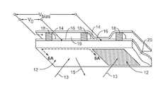
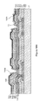
FIG. 1 shows an example of an isometric view depicting two adjacent pixels in a series of pixels of an interferometric modulator (IMOD) display device. -
FIG. 2 shows an example of a system block diagram illustrating an electronic device incorporating a 3×3 interferometric modulator display. -
FIG. 3 shows an example of a diagram illustrating movable reflective layer position versus applied voltage for the interferometric modulator ofFIG. 1 . -
FIG. 4 shows an example of a table illustrating various states of an interferometric modulator when various common and segment voltages are applied. -
FIG. 5A shows an example of a diagram illustrating a frame of display data in the 3×3 interferometric modulator display ofFIG. 2 . -
FIG. 5B shows an example of a timing diagram for common and segment signals that may be used to write the frame of display data illustrated inFIG. 5A . -
FIG. 6A shows an example of a partial cross-section of the interferometric modulator display ofFIG. 1 . -
FIGS. 6B-6E show examples of cross-sections of varying implementations of interferometric modulators. -
FIG. 7 shows an example of a flow diagram illustrating a manufacturing process for an interferometric modulator. -
FIGS. 8A-8E show examples of cross-sectional schematic illustrations of various stages in a method of making an interferometric modulator. -
FIG. 9 shows an example of a flow diagram illustrating a manufacturing process for an interferometric modulator. -
FIGS. 10A-10R show examples of cross-sectional schematic illustrations of various stages in a method of making an interferometric modulator. -
FIGS. 11A-11C show examples of plan view schematic illustrations of various interferometric modulator arrays. -
FIG. 12 shows an example of a flow diagram illustrating a manufacturing process for an interferometric modulator. -
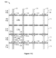
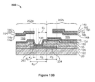
FIG. 13A shows an example of a plan view schematic illustration of an interferometric modulator array. -
FIG. 13B shows an example of a cross-sectional schematic illustration of the interferometric modulator array ofFIG. 13A taken along the line 13B-13B. -
FIG. 14 shows an example of a flow diagram illustrating a manufacturing process for an interferometric modulator. -
FIGS. 15A and 15B show examples of system block diagrams illustrating a display device that includes a plurality of interferometric modulators. - Like reference numbers and designations in the various drawings indicate like elements.
- The following detailed description is directed to certain implementations for the purposes of describing the innovative aspects. However, the teachings herein can be applied in a multitude of different ways. The described implementations may be implemented in any device that is configured to display an image, whether in motion (e.g., video) or stationary (e.g., still image), and whether textual, graphical or pictorial. More particularly, it is contemplated that the implementations may be implemented in or associated with a variety of electronic devices such as, but not limited to, mobile telephones, multimedia Internet enabled cellular telephones, mobile television receivers, wireless devices, smartphones, Bluetooth devices, personal data assistants (PDAs), wireless electronic mail receivers, hand-held or portable computers, netbooks, notebooks, smartbooks, tablets, printers, copiers, scanners, facsimile devices, GPS receivers/navigators, cameras, MP3 players, camcorders, game consoles, wrist watches, clocks, calculators, television monitors, flat panel displays, electronic reading devices (e.g., e-readers), computer monitors, auto displays (e.g., odometer display, etc.), cockpit controls and/or displays, camera view displays (e.g., display of a rear view camera in a vehicle), electronic photographs, electronic billboards or signs, projectors, architectural structures, microwaves, refrigerators, stereo systems, cassette recorders or players, DVD players, CD players, VCRs, radios, portable memory chips, washers, dryers, washer/dryers, parking meters, packaging (e.g., electromechanical systems (EMS), MEMS and non-MEMS), aesthetic structures (e.g., display of images on a piece of jewelry) and a variety of electromechanical systems devices. The teachings herein also can be used in non-display applications such as, but not limited to, electronic switching devices, radio frequency filters, sensors, accelerometers, gyroscopes, motion-sensing devices, magnetometers, inertial components for consumer electronics, parts of consumer electronics products, varactors, liquid crystal devices, electrophoretic devices, drive schemes, manufacturing processes, electronic test equipment. Thus, the teachings are not intended to be limited to the implementations depicted solely in the Figures, but instead have wide applicability as will be readily apparent to one having ordinary skill in the art.
- Electromechanical devices having improved fill factor are disclosed. The fill factor of an electromechanical device, or ratio of optically active area of the device relative to the total area of the electromechanical device, can be limited by the area of a light absorbing black mask. The electromechanical device can be an interferometric modulator device including a plurality of pixels and a mechanical layer anchored to an optical stack over the black mask at corners of each pixel. In some implementations, a conductive via is used for electrically connecting a stationary electrode of the device to the black mask. The via is offset from where the mechanical layer is anchored over the optical stack to aid in reducing the area of the black mask. For example, offsetting the via from an anchoring region used to anchor the mechanical layer over the optical stack at a pixel corner can reduce the size of the black mask at the pixel corner, since the anchoring region need not be sized to account for misalignment between the pixel via and the anchoring region. By reducing the area of the black mask at pixel corners, the optically non-active area of the array can be reduced, thereby improving fill factor. In some implementations, a via is not included in the dielectric layer of every pixel. Rather, the via can be located periodically throughout an interferometric modulator device, for example, near a corner of a pixel configured with a high gap (or cavity) height to reduce the total area of the black mask and to improve fill factor. For example, a via can be located only near a corner of a pixel (or sub-pixel) having the highest gap in a configuration that includes pixels (or sub-pixels) having various gap heights.
- In some other implementations, a conductive via is disposed in a position along an edge of a pixel in an optically non-active area of the pixel, and the via is spaced offset from the edge of the pixel in a direction towards the center of the pixel. The black mask can include a channel extending from a corner of the pixel to the via along the edge of the pixel. A side of the channel can include a widened portion (or a bulge) that is generally wider than the rest of the channel width. The bulge surrounds the footprint of the via which aids in increasing robustness of the via to process variations. In some implementations, the via need not be included along each edge of each pixel. Rather, the via can be provided for only certain edges of certain pixels, for example, in a high gap pixel along an edge shared by the high gap and a mid gap pixel, to reduce the total area of the black mask.
- Particular implementations of the subject matter described in this disclosure can be implemented to realize one or more of the following potential advantages. In some implementations, a pixel array can include improved fill factor and/or a black mask having reduced area. Additionally, some implementations can increase process robustness of a via used for electrically connecting a black mask to a stationary electrode in an interferometric device. Furthermore, some implementations can improve yield of an interferometric device by improving tolerance of the device to manufacturing variation. Moreover, some implementations can be used to reduce the number of vias in a pixel array and/or provide a pixel array having vias over only a fraction of the array.
- An example of a suitable electromechanical systems (EMS) or MEMS device, to which the described implementations may apply, is a reflective display device. Reflective display devices can incorporate interferometric modulators (IMODs) to selectively absorb and/or reflect light incident thereon using principles of optical interference. IMODs can include an absorber, a reflector that is movable with respect to the absorber, and an optical resonant cavity defined between the absorber and the reflector. The reflector can be moved to two or more different positions, which can change the size of the optical resonant cavity and thereby affect the reflectance of the interferometric modulator. The reflectance spectrums of IMODs can create fairly broad spectral bands which can be shifted across the visible wavelengths to generate different colors. The position of the spectral band can be adjusted by changing the thickness of the optical resonant cavity, i.e., by changing the position of the reflector.
-
FIG. 1 shows an example of an isometric view depicting two adjacent pixels in a series of pixels of an interferometric modulator (IMOD) display device. The IMOD display device includes one or more interferometric MEMS display elements. In these devices, the pixels of the MEMS display elements can be in either a bright or dark state. In the bright (“relaxed,” “open” or “on”) state, the display element reflects a large portion of incident visible light, e.g., to a user. Conversely, in the dark (“actuated,” “closed” or “off”) state, the display element reflects little incident visible light. In some implementations, the light reflectance properties of the on and off states may be reversed. MEMS pixels can be configured to reflect predominantly at particular wavelengths allowing for a color display in addition to black and white. - The IMOD display device can include a row/column array of IMODs. Each IMOD can include a pair of reflective layers, i.e., a movable reflective layer and a fixed partially reflective layer, positioned at a variable and controllable distance from each other to form an air gap (also referred to as an optical gap or cavity). The movable reflective layer may be moved between at least two positions. In a first position, i.e., a relaxed position, the movable reflective layer can be positioned at a relatively large distance from the fixed partially reflective layer. In a second position, i.e., an actuated position, the movable reflective layer can be positioned more closely to the partially reflective layer. Incident light that reflects from the two layers can interfere constructively or destructively depending on the position of the movable reflective layer, producing either an overall reflective or non-reflective state for each pixel. In some implementations, the IMOD may be in a reflective state when unactuated, reflecting light within the visible spectrum, and may be in a dark state when unactuated, reflecting light outside of the visible range (e.g., infrared light). In some other implementations, however, an IMOD may be in a dark state when unactuated, and in a reflective state when actuated. In some implementations, the introduction of an applied voltage can drive the pixels to change states. In some other implementations, an applied charge can drive the pixels to change states.
- The depicted portion of the pixel array in
FIG. 1 includes twoadjacent interferometric modulators 12. In theIMOD 12 on the left (as illustrated), a mechanical layer or movablereflective layer 14 is illustrated in a relaxed position at a predetermined distance from anoptical stack 16, which includes a partially reflective layer. The voltage V0 applied across theIMOD 12 on the left is insufficient to cause actuation of the movablereflective layer 14. In theIMOD 12 on the right, the movablereflective layer 14 is illustrated in an actuated position near or adjacent theoptical stack 16. The voltage Vbias applied across theIMOD 12 on the right is sufficient to maintain the movablereflective layer 14 in the actuated position. - In
FIG. 1 , the reflective properties ofpixels 12 are generally illustrated witharrows 13 indicating light incident upon thepixels 12, and light 15 reflecting from thepixel 12 on the left. Although not illustrated in detail, most of the light 13 incident upon thepixels 12 will be transmitted through thetransparent substrate 20, toward theoptical stack 16. A portion of the light incident upon theoptical stack 16 will be transmitted through the partially reflective layer of theoptical stack 16, and a portion will be reflected back through thetransparent substrate 20. The portion of light 13 that is transmitted through theoptical stack 16 will be reflected at the movablereflective layer 14, back toward (and through) thetransparent substrate 20. Interference (constructive or destructive) between the light reflected from the partially reflective layer of theoptical stack 16 and the light reflected from the movablereflective layer 14 will determine the wavelength(s) oflight 15 reflected from thepixel 12. - The
optical stack 16 can include a single layer or several layers. The layer(s) can include one or more of an electrode layer, a partially reflective and partially transmissive layer and a transparent dielectric layer. In some implementations, theoptical stack 16 is electrically conductive, partially transparent and partially reflective, and may be fabricated, for example, by depositing one or more of the above layers onto atransparent substrate 20. The electrode layer can be formed from a variety of materials, such as various metals, for example indium tin oxide (ITO). The partially reflective layer can be formed from a variety of materials that are partially reflective, such as various metals, e.g., chromium (Cr), semiconductors, and dielectrics. The partially reflective layer can be formed of one or more layers of materials, and each of the layers can be formed of a single material or a combination of materials. In some implementations, theoptical stack 16 can include a single semi-transparent thickness of metal or semiconductor which serves as both an optical absorber and conductor, while different, more conductive layers or portions (e.g., of theoptical stack 16 or of other structures of the IMOD) can serve to bus signals between IMOD pixels. Theoptical stack 16 also can include one or more insulating or dielectric layers covering one or more conductive layers or a conductive/absorptive layer. - In some implementations, the layer(s) of the
optical stack 16 can be patterned into parallel strips, and may form row electrodes in a display device as described further below. As will be understood by one having skill in the art, the term “patterned” is used herein to refer to masking as well as etching processes. In some implementations, a highly conductive and reflective material, such as aluminum (Al), may be used for the movablereflective layer 14, and these strips may form column electrodes in a display device. The movablereflective layer 14 may be formed as a series of parallel strips of a deposited metal layer or layers (orthogonal to the row electrodes of the optical stack 16) to form columns deposited on top ofposts 18 and an intervening sacrificial material deposited between theposts 18. When the sacrificial material is etched away, a definedgap 19, or optical cavity, can be formed between the movablereflective layer 14 and theoptical stack 16. In some implementations, the spacing betweenposts 18 may be approximately 1-1000 um, while thegap 19 may be on the order of less than 10,000 Angstroms (Å). - In some implementations, each pixel of the IMOD, whether in the actuated or relaxed state, is essentially a capacitor formed by the fixed and moving reflective layers. When no voltage is applied, the movable
reflective layer 14 remains in a mechanically relaxed state, as illustrated by thepixel 12 on the left inFIG. 1 , with thegap 19 between the movablereflective layer 14 andoptical stack 16. However, when a potential difference, e.g., voltage, is applied to at least one of a selected row and column, the capacitor formed at the intersection of the row and column electrodes at the corresponding pixel becomes charged, and electrostatic forces pull the electrodes together. If the applied voltage exceeds a threshold, the movablereflective layer 14 can deform and move near or against theoptical stack 16. A dielectric layer (not shown) within theoptical stack 16 may prevent shorting and control the separation distance between thelayers pixel 12 on the right inFIG. 1 . The behavior is the same regardless of the polarity of the applied potential difference. Though a series of pixels in an array may be referred to in some instances as “rows” or “columns,” a person having ordinary skill in the art will readily understand that referring to one direction as a “row” and another as a “column” is arbitrary. Restated, in some orientations, the rows can be considered columns, and the columns considered to be rows. Furthermore, the display elements may be evenly arranged in orthogonal rows and columns (an “array”), or arranged in non-linear configurations, for example, having certain positional offsets with respect to one another (a “mosaic”). The terms “array” and “mosaic” may refer to either configuration. Thus, although the display is referred to as including an “array” or “mosaic,” the elements themselves need not be arranged orthogonally to one another, or disposed in an even distribution, in any instance, but may include arrangements having asymmetric shapes and unevenly distributed elements. -
FIG. 2 shows an example of a system block diagram illustrating an electronic device incorporating a 3×3 interferometric modulator display. The electronic device includes aprocessor 21 that may be configured to execute one or more software modules. In addition to executing an operating system, theprocessor 21 may be configured to execute one or more software applications, including a web browser, a telephone application, an email program, or any other software application. - The
processor 21 can be configured to communicate with anarray driver 22. Thearray driver 22 can include arow driver circuit 24 and acolumn driver circuit 26 that provide signals to, e.g., a display array orpanel 30. The cross section of the IMOD display device illustrated inFIG. 1 is shown by the lines 1-1 inFIG. 2 . AlthoughFIG. 2 illustrates a 3×3 array of IMODs for the sake of clarity, thedisplay array 30 may contain a very large number of IMODs, and may have a different number of IMODs in rows than in columns, and vice versa. -
FIG. 3 shows an example of a diagram illustrating movable reflective layer position versus applied voltage for the interferometric modulator ofFIG. 1 . For MEMS interferometric modulators, the row/column (i.e., common/segment) write procedure may take advantage of a hysteresis property of these devices as illustrated inFIG. 3 . An interferometric modulator may use, for example, about a 10-volt potential difference to cause the movable reflective layer, or mirror, to change from the relaxed state to the actuated state. When the voltage is reduced from that value, the movable reflective layer maintains its state as the voltage drops back below, e.g., 10-volts, however, the movable reflective layer does not relax completely until the voltage drops below 2-volts. Thus, a range of voltage, approximately 3 to 7-volts, as shown inFIG. 3 , exists where there is a window of applied voltage within which the device is stable in either the relaxed or actuated state. This is referred to herein as the “hysteresis window” or “stability window.” For adisplay array 30 having the hysteresis characteristics ofFIG. 3 , the row/column write procedure can be designed to address one or more rows at a time, such that during the addressing of a given row, pixels in the addressed row that are to be actuated are exposed to a voltage difference of about 10-volts, and pixels that are to be relaxed are exposed to a voltage difference of near zero volts. After addressing, the pixels are exposed to a steady state or bias voltage difference of approximately 5-volts such that they remain in the previous strobing state. In this example, after being addressed, each pixel sees a potential difference within the “stability window” of about 3-7-volts. This hysteresis property feature enables the pixel design, e.g., illustrated inFIG. 1 , to remain stable in either an actuated or relaxed pre-existing state under the same applied voltage conditions. Since each IMOD pixel, whether in the actuated or relaxed state, is essentially a capacitor formed by the fixed and moving reflective layers, this stable state can be held at a steady voltage within the hysteresis window without substantially consuming or losing power. Moreover, essentially little or no current flows into the IMOD pixel if the applied voltage potential remains substantially fixed. - In some implementations, a frame of an image may be created by applying data signals in the form of “segment” voltages along the set of column electrodes, in accordance with the desired change (if any) to the state of the pixels in a given row. Each row of the array can be addressed in turn, such that the frame is written one row at a time. To write the desired data to the pixels in a first row, segment voltages corresponding to the desired state of the pixels in the first row can be applied on the column electrodes, and a first row pulse in the form of a specific “common” voltage or signal can be applied to the first row electrode. The set of segment voltages can then be changed to correspond to the desired change (if any) to the state of the pixels in the second row, and a second common voltage can be applied to the second row electrode. In some implementations, the pixels in the first row are unaffected by the change in the segment voltages applied along the column electrodes, and remain in the state they were set to during the first common voltage row pulse. This process may be repeated for the entire series of rows, or alternatively, columns, in a sequential fashion to produce the image frame. The frames can be refreshed and/or updated with new image data by continually repeating this process at some desired number of frames per second.
- The combination of segment and common signals applied across each pixel (that is, the potential difference across each pixel) determines the resulting state of each pixel.
FIG. 4 shows an example of a table illustrating various states of an interferometric modulator when various common and segment voltages are applied. As will be readily understood by one having ordinary skill in the art, the “segment” voltages can be applied to either the column electrodes or the row electrodes, and the “common” voltages can be applied to the other of the column electrodes or the row electrodes. - As illustrated in
FIG. 4 (as well as in the timing diagram shown inFIG. 5B ), when a release voltage VCREL is applied along a common line, all interferometric modulator elements along the common line will be placed in a relaxed state, alternatively referred to as a released or unactuated state, regardless of the voltage applied along the segment lines, i.e., high segment voltage VSH and low segment voltage VSL. In particular, when the release voltage VCREL is applied along a common line, the potential voltage across the modulator (alternatively referred to as a pixel voltage) is within the relaxation window (seeFIG. 3 , also referred to as a release window) both when the high segment voltage VSH and the low segment voltage VSL are applied along the corresponding segment line for that pixel. - When a hold voltage is applied on a common line, such as a high hold voltage VCHOLD
— H or a low hold voltage VCHOLD— L, the state of the interferometric modulator will remain constant. For example, a relaxed IMOD will remain in a relaxed position, and an actuated IMOD will remain in an actuated position. The hold voltages can be selected such that the pixel voltage will remain within a stability window both when the high segment voltage VSH and the low segment voltage VSL are applied along the corresponding segment line. Thus, the segment voltage swing, i.e., the difference between the high VSH and low segment voltage VSL, is less than the width of either the positive or the negative stability window. - When an addressing, or actuation, voltage is applied on a common line, such as a high addressing voltage VCADD
— H or a low addressing voltage VCADD— L, data can be selectively written to the modulators along that line by application of segment voltages along the respective segment lines. The segment voltages may be selected such that actuation is dependent upon the segment voltage applied. When an addressing voltage is applied along a common line, application of one segment voltage will result in a pixel voltage within a stability window, causing the pixel to remain unactuated. In contrast, application of the other segment voltage will result in a pixel voltage beyond the stability window, resulting in actuation of the pixel. The particular segment voltage which causes actuation can vary depending upon which addressing voltage is used. In some implementations, when the high addressing voltage VCADD— H is applied along the common line, application of the high segment voltage VSH can cause a modulator to remain in its current position, while application of the low segment voltage VSL can cause actuation of the modulator. As a corollary, the effect of the segment voltages can be the opposite when a low addressing voltage VCADD— L is applied, with high segment voltage VSH causing actuation of the modulator, and low segment voltage VSL having no effect (i.e., remaining stable) on the state of the modulator. - In some implementations, hold voltages, address voltages, and segment voltages may be used which produce the same polarity potential difference across the modulators. In some other implementations, signals can be used which alternate the polarity of the potential difference of the modulators. Alternation of the polarity across the modulators (that is, alternation of the polarity of write procedures) may reduce or inhibit charge accumulation which could occur after repeated write operations of a single polarity.
-
FIG. 5A shows an example of a diagram illustrating a frame of display data in the 3×3 interferometric modulator display ofFIG. 2 .FIG. 5B shows an example of a timing diagram for common and segment signals that may be used to write the frame of display data illustrated inFIG. 5A . The signals can be applied to the, e.g., 3×3 array ofFIG. 2 , which will ultimately result in the line time 60 e display arrangement illustrated inFIG. 5A . The actuated modulators inFIG. 5A are in a dark-state, i.e., where a substantial portion of the reflected light is outside of the visible spectrum so as to result in a dark appearance to, e.g., a viewer. Prior to writing the frame illustrated inFIG. 5A , the pixels can be in any state, but the write procedure illustrated in the timing diagram ofFIG. 5B presumes that each modulator has been released and resides in an unactuated state before the first line time 60 a. - During the first line time 60 a: a
release voltage 70 is applied oncommon line 1; the voltage applied oncommon line 2 begins at ahigh hold voltage 72 and moves to arelease voltage 70; and alow hold voltage 76 is applied alongcommon line 3. Thus, the modulators (common 1, segment 1), (1,2) and (1,3) alongcommon line 1 remain in a relaxed, or unactuated, state for the duration of the first line time 60 a, the modulators (2,1), (2,2) and (2,3) alongcommon line 2 will move to a relaxed state, and the modulators (3,1), (3,2) and (3,3) alongcommon line 3 will remain in their previous state. With reference toFIG. 4 , the segment voltages applied alongsegment lines common lines - During the second line time 60 b, the voltage on
common line 1 moves to ahigh hold voltage 72, and all modulators alongcommon line 1 remain in a relaxed state regardless of the segment voltage applied because no addressing, or actuation, voltage was applied on thecommon line 1. The modulators alongcommon line 2 remain in a relaxed state due to the application of therelease voltage 70, and the modulators (3,1), (3,2) and (3,3) alongcommon line 3 will relax when the voltage alongcommon line 3 moves to arelease voltage 70. - During the
third line time 60 c,common line 1 is addressed by applying ahigh address voltage 74 oncommon line 1. Because alow segment voltage 64 is applied alongsegment lines high segment voltage 62 is applied alongsegment line 3, the pixel voltage across modulator (1,3) is less than that of modulators (1,1) and (1,2), and remains within the positive stability window of the modulator; modulator (1,3) thus remains relaxed. Also duringline time 60 c, the voltage alongcommon line 2 decreases to alow hold voltage 76, and the voltage alongcommon line 3 remains at arelease voltage 70, leaving the modulators alongcommon lines - During the fourth line time 60 d, the voltage on
common line 1 returns to ahigh hold voltage 72, leaving the modulators alongcommon line 1 in their respective addressed states. The voltage oncommon line 2 is decreased to alow address voltage 78. Because ahigh segment voltage 62 is applied alongsegment line 2, the pixel voltage across modulator (2,2) is below the lower end of the negative stability window of the modulator, causing the modulator (2,2) to actuate. Conversely, because alow segment voltage 64 is applied alongsegment lines common line 3 increases to ahigh hold voltage 72, leaving the modulators alongcommon line 3 in a relaxed state. - Finally, during the fifth line time 60 e, the voltage on
common line 1 remains athigh hold voltage 72, and the voltage oncommon line 2 remains at alow hold voltage 76, leaving the modulators alongcommon lines common line 3 increases to ahigh address voltage 74 to address the modulators alongcommon line 3. As alow segment voltage 64 is applied onsegment lines high segment voltage 62 applied alongsegment line 1 causes modulator (3,1) to remain in a relaxed position. Thus, at the end of the fifth line time 60 e, the 3×3 pixel array is in the state shown inFIG. 5A , and will remain in that state as long as the hold voltages are applied along the common lines, regardless of variations in the segment voltage which may occur when modulators along other common lines (not shown) are being addressed. - In the timing diagram of
FIG. 5B , a given write procedure (i.e., line times 60 a-60 e) can include the use of either high hold and address voltages, or low hold and address voltages. Once the write procedure has been completed for a given common line (and the common voltage is set to the hold voltage having the same polarity as the actuation voltage), the pixel voltage remains within a given stability window, and does not pass through the relaxation window until a release voltage is applied on that common line. Furthermore, as each modulator is released as part of the write procedure prior to addressing the modulator, the actuation time of a modulator, rather than the release time, may determine the line time. Specifically, in implementations in which the release time of a modulator is greater than the actuation time, the release voltage may be applied for longer than a single line time, as depicted inFIG. 5B . In some other implementations, voltages applied along common lines or segment lines may vary to account for variations in the actuation and release voltages of different modulators, such as modulators of different colors. - The details of the structure of interferometric modulators that operate in accordance with the principles set forth above may vary widely. For example,
FIGS. 6A-6E show examples of cross-sections of varying implementations of interferometric modulators, including the movablereflective layer 14 and its supporting structures.FIG. 6A shows an example of a partial cross-section of the interferometric modulator display ofFIG. 1 , where a strip of metal material, i.e., the movablereflective layer 14 is deposited onsupports 18 extending orthogonally from thesubstrate 20. InFIG. 6B , the movablereflective layer 14 of each IMOD is generally square or rectangular in shape and attached to supports at or near the corners, ontethers 32. InFIG. 6C , the movablereflective layer 14 is generally square or rectangular in shape and suspended from adeformable layer 34, which may include a flexible metal. Thedeformable layer 34 can connect, directly or indirectly, to thesubstrate 20 around the perimeter of the movablereflective layer 14. These connections are herein referred to as support posts. The implementation shown inFIG. 6C has additional benefits deriving from the decoupling of the optical functions of the movablereflective layer 14 from its mechanical functions, which are carried out by thedeformable layer 34. This decoupling allows the structural design and materials used for the movablereflective layer 14 and those used for thedeformable layer 34 to be optimized independently of one another. -
FIG. 6D shows another example of an IMOD, where the movablereflective layer 14 includes areflective sub-layer 14 a. The movablereflective layer 14 rests on a support structure, such as support posts 18. The support posts 18 provide separation of the movablereflective layer 14 from the lower stationary electrode (i.e., a portion of theoptical stack 16 in the illustrated IMOD) so that agap 19 is formed between the movablereflective layer 14 and theoptical stack 16, for example when the movablereflective layer 14 is in a relaxed position. The movablereflective layer 14 also can include aconductive layer 14 c, which may be configured to serve as an electrode, and asupport layer 14 b. In this example, theconductive layer 14 c is disposed on one side of thesupport layer 14 b, distal from thesubstrate 20, and thereflective sub-layer 14 a is disposed on the other side of thesupport layer 14 b, proximal to thesubstrate 20. In some implementations, thereflective sub-layer 14 a can be conductive and can be disposed between thesupport layer 14 b and theoptical stack 16. Thesupport layer 14 b can include one or more layers of a dielectric material, for example, silicon oxynitride (SiON) or silicon dioxide (SiO2). In some implementations, thesupport layer 14 b can be a stack of layers, such as, for example, a SiO2/SiON/SiO2 tri-layer stack. Either or both of thereflective sub-layer 14 a and theconductive layer 14 c can include, e.g., an aluminum (Al) alloy with about 0.5% copper (Cu), or another reflective metallic material. Employingconductive layers dielectric support layer 14 b can balance stresses and provide enhanced conduction. In some implementations, thereflective sub-layer 14 a and theconductive layer 14 c can be formed of different materials for a variety of design purposes, such as achieving specific stress profiles within the movablereflective layer 14. - As illustrated in
FIG. 6D , some implementations also can include ablack mask structure 23. Theblack mask structure 23 can be formed in optically inactive regions (e.g., between pixels or under posts 18) to absorb ambient or stray light. Theblack mask structure 23 also can improve the optical properties of a display device by inhibiting light from being reflected from or transmitted through inactive portions of the display, thereby increasing the contrast ratio. Additionally, theblack mask structure 23 can be conductive and be configured to function as an electrical bussing layer. In some implementations, the row electrodes can be connected to theblack mask structure 23 to reduce the resistance of the connected row electrode. Theblack mask structure 23 can be formed using a variety of methods, including deposition and patterning techniques. Theblack mask structure 23 can include one or more layers. For example, in some implementations, theblack mask structure 23 includes a molybdenum-chromium (MoCr) layer that serves as an optical absorber, a silicon dioxide (SiO2) layer, and an aluminum alloy that serves as a reflector and a bussing layer, with a thickness in the range of about 30-80 Å, 500-1000 Å, and 500-6000 Å, respectively. The one or more layers can be patterned using a variety of techniques, including photolithography and dry etching, including, for example, carbon tetrafluoromethane (CF4) and/or oxygen (O2) for the MoCr and SiO2 layers and chlorine (Cl2) and/or boron trichloride (BCl3) for the aluminum alloy layer. In some implementations, theblack mask 23 can be an etalon or interferometric stack structure. In such interferometric stackblack mask structures 23, the conductive reflectors can be used to transmit or bus signals between lower, stationary electrodes in theoptical stack 16 of each row or column. In some implementations, aspacer layer 35 can serve to generally electrically isolate theabsorber layer 16 a from the conductive layers in theblack mask 23. -
FIG. 6E shows another example of an IMOD, where the movablereflective layer 14 is self supporting. In contrast withFIG. 6D , the implementation ofFIG. 6E does not include support posts 18. Instead, the movablereflective layer 14 contacts the underlyingoptical stack 16 at multiple locations, and the curvature of the movablereflective layer 14 provides sufficient support that the movablereflective layer 14 returns to the unactuated position ofFIG. 6E when the voltage across the interferometric modulator is insufficient to cause actuation. Theoptical stack 16, which may contain a plurality of several different layers, is shown here for clarity including anoptical absorber 16 a, and a dielectric 16 b. In some implementations, theoptical absorber 16 a may serve both as a fixed electrode and as a partially reflective layer. - In implementations such as those shown in
FIGS. 6A-6E , the IMODs function as direct-view devices, in which images are viewed from the front side of thetransparent substrate 20, i.e., the side opposite to that upon which the modulator is arranged. In these implementations, the back portions of the device (that is, any portion of the display device behind the movablereflective layer 14, including, for example, thedeformable layer 34 illustrated inFIG. 6C ) can be configured and operated upon without impacting or negatively affecting the image quality of the display device, because thereflective layer 14 optically shields those portions of the device. For example, in some implementations a bus structure (not illustrated) can be included behind the movablereflective layer 14 which provides the ability to separate the optical properties of the modulator from the electromechanical properties of the modulator, such as voltage addressing and the movements that result from such addressing. Additionally, the implementations ofFIGS. 6A-6E can simplify processing, such as, e.g., patterning. -
FIG. 7 shows an example of a flow diagram illustrating amanufacturing process 80 for an interferometric modulator, andFIGS. 8A-8E show examples of cross-sectional schematic illustrations of corresponding stages of such amanufacturing process 80. In some implementations, themanufacturing process 80 can be implemented to manufacture, e.g., interferometric modulators of the general type illustrated inFIGS. 1 and 6 , in addition to other blocks not shown inFIG. 7 . With reference toFIGS. 1 , 6 and 7, theprocess 80 begins atblock 82 with the formation of theoptical stack 16 over thesubstrate 20.FIG. 8A illustrates such anoptical stack 16 formed over thesubstrate 20. Thesubstrate 20 may be a transparent substrate such as glass or plastic, it may be flexible or relatively stiff and unbending, and may have been subjected to prior preparation processes, e.g., cleaning, to facilitate efficient formation of theoptical stack 16. As discussed above, theoptical stack 16 can be electrically conductive, partially transparent and partially reflective and may be fabricated, for example, by depositing one or more layers having the desired properties onto thetransparent substrate 20. InFIG. 8A , theoptical stack 16 includes a multilayer structure having sub-layers 16 a and 16 b, although more or fewer sub-layers may be included in some other implementations. In some implementations, one of the sub-layers 16 a, 16 b can be configured with both optically absorptive and conductive properties, such as the combined conductor/absorber sub-layer 16 a. Additionally, one or more of the sub-layers 16 a, 16 b can be patterned into parallel strips, and may form row electrodes in a display device. Such patterning can be performed by a masking and etching process or another suitable process known in the art. In some implementations, one of the sub-layers 16 a, 16 b can be an insulating or dielectric layer, such assub-layer 16 b that is deposited over one or more metal layers (e.g., one or more reflective and/or conductive layers). In addition, theoptical stack 16 can be patterned into individual and parallel strips that form the rows of the display. - The
process 80 continues atblock 84 with the formation of asacrificial layer 25 over theoptical stack 16. Thesacrificial layer 25 is later removed (e.g., at block 90) to form thecavity 19 and thus thesacrificial layer 25 is not shown in the resultinginterferometric modulators 12 illustrated inFIG. 1 .FIG. 8B illustrates a partially fabricated device including asacrificial layer 25 formed over theoptical stack 16. The formation of thesacrificial layer 25 over theoptical stack 16 may include deposition of a xenon difluoride (XeF2)-etchable material such as molybdenum (Mo) or amorphous silicon (Si), in a thickness selected to provide, after subsequent removal, a gap or cavity 19 (see alsoFIGS. 1 and 8E ) having a desired design size. Deposition of the sacrificial material may be carried out using deposition techniques such as physical vapor deposition (PVD, e.g., sputtering), plasma-enhanced chemical vapor deposition (PECVD), thermal chemical vapor deposition (thermal CVD), or spin-coating. - The
process 80 continues atblock 86 with the formation of a support structure e.g., apost 18 as illustrated inFIGS. 1 , 6 and 8C. The formation of thepost 18 may include patterning thesacrificial layer 25 to form a support structure aperture, then depositing a material (e.g., a polymer or an inorganic material, e.g., silicon oxide) into the aperture to form thepost 18, using a deposition method such as PVD, PECVD, thermal CVD, or spin-coating. In some implementations, the support structure aperture formed in the sacrificial layer can extend through both thesacrificial layer 25 and theoptical stack 16 to theunderlying substrate 20, so that the lower end of thepost 18 contacts thesubstrate 20 as illustrated inFIG. 6A . Alternatively, as depicted inFIG. 8C , the aperture formed in thesacrificial layer 25 can extend through thesacrificial layer 25, but not through theoptical stack 16. For example,FIG. 8E illustrates the lower ends of the support posts 18 in contact with an upper surface of theoptical stack 16. Thepost 18, or other support structures, may be formed by depositing a layer of support structure material over thesacrificial layer 25 and patterning to remove portions of the support structure material located away from apertures in thesacrificial layer 25. The support structures may be located within the apertures, as illustrated inFIG. 8C , but also can, at least partially, extend over a portion of thesacrificial layer 25. As noted above, the patterning of thesacrificial layer 25 and/or the support posts 18 can be performed by a patterning and etching process, but also may be performed by alternative etching methods. - The
process 80 continues atblock 88 with the formation of a movable reflective layer or membrane such as the movablereflective layer 14 illustrated inFIGS. 1 , 6 and 8D. The movablereflective layer 14 may be formed by employing one or more deposition steps, e.g., reflective layer (e.g., aluminum, aluminum alloy) deposition, along with one or more patterning, masking, and/or etching steps. The movablereflective layer 14 can be electrically conductive, and referred to as an electrically conductive layer. In some implementations, the movablereflective layer 14 may include a plurality of sub-layers 14 a, 14 b, 14 c as shown inFIG. 8D . In some implementations, one or more of the sub-layers, such as sub-layers 14 a, 14 c, may include highly reflective sub-layers selected for their optical properties, and another sub-layer 14 b may include a mechanical sub-layer selected for its mechanical properties. Since thesacrificial layer 25 is still present in the partially fabricated interferometric modulator formed atblock 88, the movablereflective layer 14 is typically not movable at this stage. A partially fabricated IMOD that contains asacrificial layer 25 also may be referred to herein as an “unreleased” IMOD. As described above in connection withFIG. 1 , the movablereflective layer 14 can be patterned into individual and parallel strips that form the columns of the display. - The
process 80 continues atblock 90 with the formation of a cavity, e.g.,cavity 19 as illustrated inFIGS. 1 , 6 and 8E. Thecavity 19 may be formed by exposing the sacrificial material 25 (deposited at block 84) to an etchant. For example, an etchable sacrificial material such as molybdenum (Mo) or amorphous silicon (a-Si) may be removed by dry chemical etching, e.g., by exposing thesacrificial layer 25 to a gaseous or vaporous etchant, such as vapors derived from solid xenon difluoride (XeF2) for a period of time that is effective to remove the desired amount of material, typically selectively removed relative to the structures surrounding thecavity 19. Other etching methods, e.g. wet etching and/or plasma etching, also may be used. Since thesacrificial layer 25 is removed duringblock 90, the movablereflective layer 14 is typically movable after this stage. After removal of thesacrificial material 25, the resulting fully or partially fabricated IMOD may be referred to herein as a “released” IMOD. - Electromechanical devices having improved fill factor are disclosed. In some implementations, the electromechanical device can be an interferometric device including a pixel array and a mechanical layer that is anchored over an optical stack at each corner of each pixel. A via can be provided in a pixel of the array to electrically connect a stationary electrode to the black mask at a corner of the pixel. The via can be offset from where the mechanical layer is anchored over the optical stack at the corner of the pixel in an optically non-active area of the pixel. Offsetting the via can reduce the area of the black mask relative to a design in which the via overlaps with an anchoring hole used to anchor the mechanical layer over the optical stack, and thus the offset via can be employed in a pixel array to improve fill factor. For example, offsetting the via from the anchor hole can reduce the size of the anchor hole, thereby permitting the area of the black mask at pixel corners to be decreased. Thus, offsetting the via from the anchor hole can increase fill factor by reducing black mask area, thereby improving fill factor by increasing the ratio of optically active area in the pixel array relative to the total area of the array. In some implementations, the via is provided for only some of the pixels (or a fraction of the pixels), thereby further improving fill factor of the pixel array. For example, the via can only be provided at a corner of a pixel with the largest gap size.
-
FIG. 9 shows an example of a flow diagram illustrating amanufacturing process 100 for an interferometric modulator. Theprocess 100 starts at ablock 102. In ablock 104, a black mask is formed over a substrate. The substrate can be, for example, a transparent substrate including glass or plastic. The black mask can include a variety of materials and/or layers, including glass or a transparent polymeric material which permits images to be viewed through the substrate. - With continuing reference to
FIG. 9 , the black mask structure can be configured to absorb ambient or stray light in optically inactive regions, such as regions between pixels and/or regions near pixel corners where the mechanical layer bends so as to improve the optical properties of a display device. Additionally, the black mask structure can be conductive and be configured to function as an electrical bussing layer. The black mask structure can include a plurality of layers, as described above. - In a
block 106, a dielectric layer is provided over the black mask. The dielectric layer can be used to electrically isolate portions of the black mask from one or more subsequently deposited layers. The dielectric layer can be any suitable electrical insulator, including, for example, silicon dioxide (SiO2), silicon oxynitride (SiON) and/or tetraethyl orthosilicate (TEOS). - The
process 100 illustrated inFIG. 9 continues at ablock 108, in which a via is formed in the dielectric layer to the black mask. The via can permit a subsequently deposited layer to contact the black mask to aid in providing, for example, electrical connections for rows in the interferometric modulator array. As will be described in further detail below, vias need not be included for each pixel of the interferometric modulator array. Rather, vias can be provided only for a portion of the pixels of the array to aid in increasing fill factor. - In a
block 110, an optical stack is formed over the dielectric layer and via. The optical stack includes a stationary electrode, and the portion of the optical stack provided over the via can be used to make electrical connections between the stationary electrode and the black mask. - The
process 100 illustrated inFIG. 9 continues to ablock 112, in which a sacrificial layer is formed over the optical stack. The sacrificial layer is later removed to form a gap. The formation of the sacrificial layer over the optical stack may include deposition of a fluorine-etchable material such as molybdenum (Mo) or amorphous silicon (a-Si), in a thickness selected to provide, after subsequent removal, a gap having the desired size. Multiple sacrificial layers can be deposited to achieve a plurality of gap sizes. For example, for an IMOD array, each gap size can represent a different reflected color. - In a
block 114, an anchoring hole is formed in the sacrificial layer that is offset from the via. The anchoring hole can be formed by removing a portion of the sacrificial layer near a corner of a pixel. The anchoring hole can used to form a post for supporting a subsequently deposited mechanical layer and/or to permit a self-supporting mechanical layer to contact the optical stack and/or another layer, as will be described in detail below. The anchoring hole formed inblock 114 is not aligned with the via formed inblock 110. Rather, the anchoring hole and via are offset, thereby permitting the anchoring hole to have dimensions which are smaller relative to a scheme in which the via and the anchoring hole overlap, since the anchoring hole need not include additional margin to account for alignment with the via. Reducing the dimensions of the anchoring hole can aid in improving fill factor of the interferometric modulator array, since reducing the size of the anchoring hole permits the area of the optically non-active black mask disposed at the pixel corner to be decreased. - The
process 100 illustrated inFIG. 9 continues at ablock 116 with the formation of a mechanical layer. The mechanical layer can be formed by employing one or more deposition steps, along with one or more patterning, masking, and/or etching steps, as was described earlier. - The
process 100 illustrated inFIG. 9 continues at ablock 118 with the formation of a cavity or gap. The gap may be formed by exposing the sacrificial material, such as the sacrificial material deposited at theblock 112, to an etchant. For example, an etchable sacrificial material such as molybdenum (Mo), tungsten (W), tantalum (Ta) or polycrystalline silicon (poly-Si) or amorphous silicon (a-Si) may be removed by dry chemical etching. - After the sacrificial layer is removed, the mechanical layer is typically released and can be moved by electrostatic forces between an actuated and a relaxed position by application of a voltage between the stationary electrode and the mechanical layer. The mechanical layer can be anchored at the corner of a pixel to the optical stack over a portion of the black mask formed in the
block 104. - The
process 100 illustrated inFIG. 9 ends at a block 119. Additional details of the method can be as described below. Many additional steps may be employed before, in the middle of, or after the illustrated sequence, but are omitted for clarity. -
FIGS. 10A-10R show examples of cross-sectional schematic illustrations of various stages in a method of making an interferometric modulator. InFIG. 10A , ablack mask structure 23 has been provided over asubstrate 20. Thesubstrate 20 can include a variety of transparent materials, as was described above. One or more layers can be provided on the substrate before providing theblack mask structure 23. For example, as shown inFIG. 10A , an etch-stop layer 122 has been provided before providing theblack mask structure 23 to serve as an etch-stop when patterning the black mask. In some implementations, the etch-stop layer 122 is an aluminum oxide layer having a thickness in the range of about 50-250 Å, for example, about 160 Å. - The
black mask structure 23 can be configured to absorb ambient or stray light in optically inactive regions (e.g., between pixels) to improve the optical properties of a display device by increasing the contrast ratio. Additionally, theblack mask structure 23 can be conductive and be configured to function as an electrical bussing layer. - With continuing reference to
FIG. 10A , theblack mask structure 23 can include one or more layers. In some implementations, theblack mask structure 23 includes anoptical absorber layer 23 a, adielectric layer 23 b, and a bussing layer 23 c. In some implementations, a MoCr layer serves as theoptical absorber layer 23 a, a SiO2 layer serves as thedielectric layer 23 b, and an aluminum alloy layer serves as the bussing layer 23 c, with a thickness in the range of, for example, about 30-80 Å, 500-1000 Å, and 500-6000 Å, respectively. -
FIG. 10B illustrates providing ashaping structure 126 over thesubstrate 20. The shapingstructure 126 can include a buffer oxide layer, such as silicon dioxide (SiO2). The shapingstructure 126 can have, for example, a thickness in the range of about 500-6000 Å. The shapingstructure 126 can aid in maintaining a relatively planar profile across the substrate by filling in gaps between bussing orblack mask structures 23. However, the shapingstructure 126 can overlap a portion of theblack mask structure 23 to aid in forming a kink in the mechanical layer, as will be described in detail later below. In particular, one or more layers, including the mechanical layer, can be deposited over the shapingstructure 126, thereby substantially replicating one or more geometric features of the shapingstructure 126. For example, as illustrated inFIG. 10B , the shapingstructure 126 can overlap theblack mask structure 23 to form aprotrusion 129, which can produce an upwardly extending wave or kink in a subsequently deposited conformal layer, such as a mechanical layer. - Although various electromechanical systems devices illustrated herein are shown and described as including the shaping
structure 126, persons having ordinary skill in the art will recognize that the methods of forming a mechanical layer as described herein can be applicable to processes lacking the shapingstructure 126. -
FIG. 10C illustrates providing a spacer ordielectric layer 35. Thedielectric layer 35 can include, for example, silicon dioxide (SiO2), silicon oxynitride (SiON), and/or tetraethyl orthosilicate (TEOS). In some implementations, the thickness of thedielectric layer 35 is in the range of about 3000-6000 Å, however, thedielectric layer 35 can have a variety of thicknesses depending on desired optical properties. Thedielectric layer 35 can be removed over a portion above the black mask structure 23 (“above” here referring to the side of theblack mask structure 23 opposite the substrate 20), so as to permit formation of a via for electrically connecting a stationary electrode to theblack mask structure 23, as will be described in further detail below with reference toFIGS. 10E and 10F . -
FIG. 10D illustrates providing acolor enhancement structure 134 over thedielectric layer 35. Thecolor enhancement structure 134 can be selectively provided over various pixel structures. For example, in a multi-color interferometric modulator implementation employing multiple gap heights, thecolor enhancement structure 134 can be provided over modulators having a particular gap size. In some implementations, thecolor enhancement structure 134 is a silicon oxynitride (SiON) layer having a thickness ranging between about 1500 Å to about 2500 Å, for example, about 1900 Å. The SiON layer can be patterned using any suitable technique, including, for example, an etch process employing tetrafluoromethane (CF4) and/or oxygen (O2). - One or more layers can be provided on the
dielectric layer 35 before providing thecolor enhancement structure 134. For example, as shown inFIG. 10D , an etch-stop layer 135 has been provided before providing thecolor enhancement layer 134. In some implementations, theetch stop layer 135 is an aluminum oxide layer having a thickness in the range of about 50-250 Å, for example, about 160 Å. -
FIG. 10E illustrates forming a via 138 in thedielectric layer 35. The via 138 can permit a subsequently deposited layer to contact theblack mask structure 23, as will be described in detail below. As shown inFIG. 10E , vias need not be included over each region of theblack mask 23. Rather, vias can be placed periodically in the interferometric modulator so as to increase the fill factor of the array. -
FIGS. 10F and 10G illustrate forming anoptical stack 16 over thedielectric layer 35 and thevia 138. Theoptical stack 16 can include a plurality of layers. For example, theoptical stack 16 can include astationary electrode layer 140, such as molybdenum-chromium (MoCr), atransparent dielectric layer 141, such as silicon dioxide (SiO2), and an etch-stop layer 142, such as aluminum oxide (AlOx), for protecting thetransparent dielectric layer 141 during subsequent sacrificial layer etch processes and/or attack during sacrificial layer removal processes. The etch-stop layer 142 can be formed from a variety of materials that are partially reflective such as various metals, semiconductors, and dielectrics. The partially reflective layer can be formed of one or more sub-layers, and each of the sub-layers can be formed of a single material or a combination of materials. In some implementations, some or all of the layers of theoptical stack 16, including, for example, thestationary electrode 140, are patterned into parallel strips, and may form row electrodes in a display device. As illustrated inFIGS. 10F and 10G , one or more layers of theoptical stack 16 may physically and electrically contact theblack mask structure 23. For example, the via 138 permits thestationary electrode 140 to electrically contact theblack mask structure 23. -
FIGS. 10H-10J illustrate providing and patterning a plurality of sacrificial layers over theoptical stack 16. The sacrificial layers are later removed to form a gap or cavity, as will be discussed below. The use of a plurality of sacrificial layers can aid in the formation of a display device having a multitude of resonant optical gaps. For example, as illustrated, various gap sizes can be created by selectively providing a firstsacrificial layer 144, a secondsacrificial layer 145, and a thirdsacrificial layer 146. This can provide a first gap size (or “high gap”) equal to about a sum of the thicknesses of the first, second and third sacrificial layers 144-146, a second gap size (or “mid gap”) equal to about a sum of the thicknesses of the second and thirdsacrificial layers sacrificial layer 146. For an interferometric modulator array, a high gap can correspond to a high gap pixel, a mid gap can correspond to a mid gap pixel, and a low gap can correspond to a low gap pixel. Each of these pixels that are configured with different gap size can produce a different reflected color. Accordingly, such pixels may be referred to herein as high, mid, or low gap pixels. - The formation of the first, second and third sacrificial layers 144-146 over the
optical stack 16 may include deposition of molybdenum (Mo) or amorphous silicon (a-Si). In some implementations, the firstsacrificial layer 144 is a molybdenum (Mo) layer having a thickness ranging between about 200 Å to about 1,000 Å, for example, about 400 Å, the secondsacrificial layer 145 is a Mo layer having a thickness ranging between about 200 Å to about 1,000 Å, for example, about 400 Å, and the thirdsacrificial layer 146 is a Mo layer having a thickness ranging between about 600 Å to about 2,000 Å, for example, about 1,600 Å. - Although
FIGS. 10H-10J are illustrated for a configuration in which the secondsacrificial layer 145 is provided over the firstsacrificial layer 144 and the thirdsacrificial layer 146 is provided over the first and secondsacrificial layers -
FIG. 10K illustrates patterning the sacrificial layers 144-146 between pixels. The sacrificial layers can be patterned in a variety of ways, including using an etchant, such as chlorine (Cl2) and/or oxygen (O2). The portion of the sacrificial layers 144-146 removed between pixels, such as at the corners of pixels, can createanchor holes 150, which can be used to form a post for supporting a subsequently deposited mechanical layer and/or to aid in anchoring a self-supporting mechanical layer, as will be described below. - The anchor holes 150 of the illustrated partially fabricated interferometric modulator are not aligned with the via 138. This can permit the
anchor hole 150 to have a width w1 which is smaller relative to a scheme in which the via 138 and theanchor hole 150 overlap to form an anchor via, since theanchor hole 150 need not include additional margin to account for alignment with via 138. Additionally, by offsetting the via 138 and theanchor hole 150, non-uniformity across pixels related to anchor hole and via misalignment can be avoided. - Furthermore, as illustrated in
FIG. 10L , in some implementations the via 138 need not be included over each region of theblack mask 23. Rather, vias can be periodically provided over less than all of the pixels of an array. By reducing the width w1 of theanchor hole 150 and by reducing the total number ofvias 138 in the interferometric modulator array, the total area of theblack mask 23 can be reduced, thereby improving the fill factor. -
FIG. 10L illustrates providing and patterning areflective layer 14 a and asupport layer 14 b of a mechanical layer. Thereflective layer 14 a can be a reflective material including, for example, aluminum alloys. In some implementations, thereflective layer 14 a includes aluminum-copper (AlCu) having copper by weight in the range of about 0.3% to 1.0%, for example, about 0.5%. Thereflective layer 14 a can be any suitable thickness, such as a thickness in the range of about 200 Å to about 500 Å, for example, about 300 Å. - The
support layer 14 b can be used to assist a photolithography process by serving as an antireflection layer and/or to aid in obtaining a desired mechanical flexibility of a fully fabricated mechanical layer. In some implementations, thesupport layer 14 b is a silicon oxynitride (SiON) layer having a thickness in the range of about 50 Å to about 1,000 Å, for example, about 250 Å. -
FIG. 10M illustrates providing an etch-stop layer 154 over thesupport layer 14 b, over thetransparent dielectric layer 141 on the bottom of anchor holes 150, and over the sacrificial layers 144-146 on the sidewalls of the anchor holes 150. The etch-stop layer 154 can be, for instance, an aluminum oxide (AlOx) layer having a thickness in the range of about 100 Å to about 300 Å, for example, 200 Å. The etch-stop layer 154 can be employed to protect layers of the interferometric device from subsequent etching steps. For example, as will be described later below, when the sacrificial layers 144-146 are removed to release the mechanical layer, the etch-stop layer 154 can protect support layers from an etchant used to remove the sacrificial layers 144-146. -
FIGS. 10N-10P illustrate providing and patterning afirst support layer 160, asecond support layer 161, and athird support layer 162. The first, second, and third support layers 160-162 can be used for a variety of functions. For example, the first, second, and third support layers 160-162 can be used to form support structures, including posts and/or rivets. Furthermore, the first, second, and third support layers 160-162 can be incorporated into all or part of the mechanical layer to aid in achieving a structural rigidity corresponding to a desired actuation voltage and/or to aid in obtaining a self-supporting mechanical layer. - As illustrated in
FIG. 10P , aportion 160 a of thefirst support layer 160 can serve as a support post for a high gap pixel and a mid gap pixel, while aportion 160 b of thefirst support layer 160 can be included in the mechanical layer of a low gap pixel. By employing the first, second and third support layers 160-162 to serve a variety of functions across pixels of varying gap heights, flexibility in the design of the interferometric device can be improved. In some implementations, the mechanical layer can be self-supporting over certain pixels and can be supported by a support post or other structures over other pixels. - The sacrificial layers 144-146 can be later removed to form various pixels in the interferometric modulator array. The thickness of the mechanical layer formed above the sacrificial layers can be varied by selectively including the first, second and third support layers 160-162 in the mechanical layer over various pixels of the array. For example, the
third support layer 162 can be provided over high gap, mid gap and low gap pixels, thesecond support layer 161 can be provided over mid and low gap pixels, and thefirst support layer 160 can be provided over low gap pixels. By varying the thickness of the mechanical layer across pixels of different gap heights, the desired stiffness of the mechanical layer can be achieved for each gap height, which can aid in permitting the same pixel actuation voltage for different sized air-gaps for color display applications. - The first, second and third support layers 160-162 can be formed by a dielectric material, such as silicon oxynitride (SiON). In some implementations, the thickness of the first, second and third supporting layers 160-162 can each be in the range of about 600 Å to about 3,000 Å, for example, about 1,000 Å.
-
FIG. 10Q illustrates providing and patterning acap layer 14 c to form a completedmechanical layer 14. Thecap layer 14 c can be provided conformally over the supporting layers 160-162 and can have a pattern similar to that of thereflective layer 14 a. Patterning thecap layer 14 c similar to that of thereflective layer 14 a can aid in balancing stresses in themechanical layer 14. By balancing stresses in themechanical layer 14, the shaping and curvature of themechanical layer 14 upon removal of the sacrificial layers 144-146 can be controlled, as will be described below. Furthermore, balanced stresses in themechanical layer 14 can reduce the sensitivity of gap height of a released interferometric modulator to temperature. - The
cap layer 14 c can be a metallic material and can be, for example, the same material as thereflective layer 14 a. In some implementations, thecap layer 14 c includes aluminum-copper (AlCu) having copper by weight in the range of about 0.3% to 1.0%, for example, about 0.5%, and the thickness of thecap layer 14 c is selected to be in the range of about 200 Å to about 500 Å, for example, about 300 Å. - As was described above the
mechanical layer 14 can include a variety of layers across different pixels of the interferometric modulator array. Additional details of themechanical layer 14 can be as described below. -
FIG. 10R illustrates removal of the sacrificial layers 144-146 to form a first orhigh gap 19 a, a second ormid gap 19 b, and a third or low gap 19 c. Additional steps can be employed before forming first, second andthird gaps 19 a-19 c. For example, sacrificial release holes can be formed in themechanical layer 14 to aid in removing the sacrificial layers 144-146. - The
gaps 19 a-19 c can be formed by exposing the sacrificial layers 144-146 to an etchant, as was described above. The sacrificial layer can be exposed for a period of time that is effective to remove the material, typically selectively relative to the structures surrounding thegaps 19 a-19 c. Other selective etching methods, for example, wet etching and/or plasma etching, also can be used. - The etch-
stop layer 154 can protect thefirst support layer 160 from the sacrificial release chemistry used to remove the sacrificial layers 144-146. This can permit thefirst support layer 160 to be a structural material that would otherwise be etched by the release chemistry used to remove the sacrificial layers. - The
dielectric protection layer 142 can protect layers of theoptical stack 16, such as thedielectric layer 141, from the sacrificial release chemistry used to remove the sacrificial layers 144-146. Inclusion of thedielectric protection layer 142 can aid reducing or preventing damage to the optical stack during release, thereby improving optical performance. - The first, second and
third gaps 19 a-19 c can correspond to cavities that interferometrically enhance different colors. For example, the first, second andthird gaps 19 a-19 c can have heights selected to interferometrically enhance, for example, blue, red, and green, respectively. The first orhigh gap 19 a can be associated with a first orhigh gap pixel 172 a, the second ormid gap 19 b can be associated with a second ormid gap pixel 172 b, and the third or low gap 19 c can be associated with a third orlow gap pixel 172 c. - In order to permit approximately the same actuation voltage to collapse the mechanical layer for each gap size, the
mechanical layer 14 can include different materials, number of layers, or thicknesses over each of thegaps 19 a-19 c. Thus, as shown inFIG. 10R , a portion of themechanical layer 14 over thehigh gap 19 a can include thereflective layer 14 a, thesupport layer 14 b, the etch-stop layer 154, thethird support layer 162 and thecap layer 14 c, while a portion of themechanical layer 14 over themid gap 19 b can further include thesecond support layer 161. Similarly, in contrast to the portion of themechanical layer 14 over thehigh gap 19 a, a portion of themechanical layer 14 over the low gap 19 c can further include the first and second support layers 160, 161. - As described above, the first, second and third support layers 160-162 can serve different functions across different pixels of the interferometric modulator array. For example, the
first support layer 160 can be used for supporting themechanical layer 14 over high and mid gap pixels and for increasing the structural rigidity of low gap pixels. Additionally, thesecond support layer 161 can be used for supporting themechanical layer 14 over high gap pixels and for increasing the structural rigidity of mid gap pixels, and the third support layer can be used for increasing the structural rigidity of low, mid and high gap pixels. Thus, thefirst portion 160 a of thefirst support layer 160 serves as a post for supporting themechanical layer 14 over the high andmid gaps second portion 160 b of thefirst support layer 160 is included in themechanical layer 14 over the low gap 19 c. Using a plurality of support layers permits approximately the same actuation voltage to collapse the mechanical layer for each gap size. - After removal of the sacrificial layers 144-146, the
mechanical layer 14 can become displaced away from the substrate by a launch height and can change shape or curvature at this point for a variety of reasons, such as residual mechanical stresses. As described above, thecap layer 14 c can be used with thereflective layer 14 a to aid in balancing the stresses in the mechanical layer when released. Thus, thecap layer 14 c can have a thickness, composition, and/or stress selected to aid in tuning the launch and curvature of the mechanical layer upon removal of the sacrificial layers 144-146. Additionally, providing themechanical layer 14 over the shapingstructure 126, and particularly over theprotrusion 129 ofFIG. 10B , akink 171 is formed in themechanical layer 14. The geometric features of thekink 171 can be controlled by varying the thickness of the shapingstructure 126, thereby controlling the stresses in themechanical layer 14. Control of the launch height can allow the selection of a sacrificial layer thickness needed for a particular gap size which is desirable from a fabrication and optical performance standpoint. - As was described above, the anchor holes 150 of
FIG. 10K are not aligned with the via 138. Thus, as shown inFIG. 10R , themechanical layer 14 is anchored to theoptical stack 16 over theblack mask 23 at a point offset from thevia 138. As described above, anchoring themechanical layer 14 at a point offset from the via 138 can permit theblack mask 23 to be smaller relative to a design in which themechanical layer 14 is anchored over theblack mask 23 in the same region as the via is located. For example, by offsetting the via 138 from an anchoring hole used to anchor themechanical layer 14, the size of the anchor hole need not have increased area to account for process alignment with the via 138. Additionally, by offsetting the via 138 from the anchor hole used to secure themechanical layer 14, non-uniformity across pixels related to anchor hole and via misalignment can be avoided. Thus, by offsetting the via 138 from the anchor hole fill factor of the interferometric modulator array can be improved. - Furthermore, as illustrated in
FIG. 10R , the via 138 need not be included in each pixel. Rather, the vias can be provided over less than all of the pixels of an array. For example, as shown inFIG. 10R , the via 138 has been included near acorner 123 of thehigh gap pixel 172 a. Furthermore, vias have not been included at corners ofmid gap pixel 172 b orlow gap pixel 172 c. By providing vias for less than all of the pixels of the array, the total number of vias in the interferometric modulator array can be reduced, which in turn can reduce the total area of theblack mask 23. Since theblack mask 23 is optically opaque, reducing the total area of theblack mask 23 improves the fill factor of the pixel array. - As illustrated in
FIG. 10R , theblack mask 23 has a footprint larger than the footprint of the structures used to support themechanical layer 14. For example, theportion 160 a of thefirst support layer 160 operates as a support post for the portion of themechanical layer 14 associated with thehigh gap pixel 172 a, and has a width less than that of theblack mask 23 at thecorner 123 of thehigh gap pixel 172 a. The additional width of theblack mask 23 around the anchoring region of the mechanical layer can mask a bending portion of themechanical layer 14 during actuation. For example, when themechanical layer 14 is actuated, while most of themechanical layer 14 can be aligned in a plane and can be in contact with theoptical stack 16, a portion of the mechanical layer 14 (e.g., along edges of a pixel) may not be in contact with theoptical stack 16, and thus can interferometrically produce an undesired color if additional black mask is not provided. The portion of themechanical layer 14 out of contact with theoptical stack 16 during actuation can increase for pixels having larger gap heights. For example, the bending region of thehigh gap pixel 172 a can be greater than that of thelow gap pixel 172 c, because thegap 19 a is larger than the gap 19 c. - In some implementations, vias, such as the via 138, are included at one or more corners of pixels of the largest gap size. Positioning the
vias 138 near corners of pixels of the largest gap size can be advantageous because high gap pixels can have a larger bending region in the actuated state, and thus can have a larger optically inactive area at pixel corners relative to mid and low gap pixels. Thus, in some implementations, the black mask can be larger at corners of high gap sub-pixels to account for the larger bending region and to provide room for a via. However, since the vias need not be included for each pixel of the array, the total area of theblack mask 23 can be reduced, and the fill factor of the interferometric modulator array can be improved. - The vias, such as the via 138, can have a variety of shape and sizes. For example, the vias can be shaped as a circle, oval, octagon and/or any other suitable shape. The size of the vias can vary with process. In some implementations, each via 138 has a largest width in the range of about 1.5 μm to about 3.0 μm, for example, about 2.4 μm. Additional details of the vias can be as described below.
-
FIGS. 11A-11C show examples of plan view schematic illustrations of various interferometric modulator arrays. InFIG. 11A , aninterferometric modulator array 180 is illustrated. Theinterferometric modulator array 180 includes a plurality of pixels of different gap sizes, including a first gap orhigh gap pixel 174 a, a second gap ormid gap pixel 174 b, and a third gap or low gap pixel 174 c. The high, mid and low gap pixels 174 a-174 c can be similar to the high, mid, and low gap pixels 172 a-172 c ofFIG. 10R . However, the high, mid and low gap pixels 174 a-174 c need not be identical to the high, mid, and low gap pixels 172 a-172 c. - As shown in
FIG. 11A , an electrically conductive black mask is disposed on the substrate at each corner of the high, mid and low gap pixels 174 a-174 c. Although not illustrated inFIG. 11A , a dielectric layer has been provided over the black mask, and an optical stack including a stationary electrode has been provided over the dielectric layer. Thevias 138 are used to electrically contact the stationary electrode of the optical stack to various portions of theblack mask 23. - The
mechanical layer 14 is positioned over the optical stack to define the gap heights of the high, mid, and low gap pixels 174 a-174 c. Themechanical layer 14 is anchored over theblack mask 23 at each of the corners of the high, mid and low pixels 174 a-174 c. For example, thehigh gap pixel 174 a includes fourcorners 123 a-123 d, and the mechanical layer is anchored over the optical stack at each of the fourcorners holes mechanical layer 14 can be anchored over the black mask in a multitude of ways. - The area of the
black mask 23 surrounding each corner of each pixel need not be the same for each pixel of thearray 180. Rather, the area of black mask at a pixel corner can be larger for pixels having a relatively larger gap, such as pixels of the largest gap size, so as to account for increased mechanical layer bending during actuation. For example, the area of the black mask at each of thecorners 123 a-123 d of thehigh gap pixel 174 a is larger than the area of the black mask at acorner 123 e of themid gap pixel 174 b and area of the black mask at acorner 123 f of the low gap pixel 174 c. As shown inFIG. 11A , the increased portion or bulge of the black mask at thecorner 123 a of thehigh gap pixel 174 a can be used for providing the via 138. - With continuing reference to
FIG. 11A , in some implementations, the via 138 is positioned at a corner of thehigh gap pixel 174 a adjacent a mid gap pixel. However, as will be described below with reference toFIGS. 11B and 11C , the via 138 can be provided in other locations and/or at multiple corners of high gap pixels. - The distance to the edge of the black mask along a line from the center of the anchoring hole to the center of a pixel can vary depending on the gap height of the pixel. For example, the distance d1 from the edge of the black mask along a line to the center of the anchoring hole of a high gap pixel can be in the range of about 10 μm to about 12 μm, while the distance d2 from the edge of the black mask along a line to the center of the anchoring hole of a low or mid gap pixel can be in the range of about 7 μm to about 9 μm.
- With continuing reference to
FIG. 11A , theblack mask 23 can be included in other regions of a pixels, such as along pixel edges, in addition to being provided at pixel corners. The black mask regions along the edges of pixels also can be used to provide electrical connections along a row or column, and can include breaks along one or more edges of each pixel to provide the desired electrical connectivity. For example, theblack mask 23 includes a break along an edge bordering thehigh gap pixel 174 a and the low gap pixel 174 c. In some implementations, the breaks have a length in the range of about 2 μm to about 3 μm. - As described above, the
interferometric device array 180 includes vias offset from the anchoring holes or other structures used to secure themechanical layer 14. For example, a via 138 at thecorner 123 a of thehigh gap pixel 174 a is offset from theanchor hole 150 a. In some implementations, distance from the center of the via to the center of the anchoring hole to which the mechanical layer is secured ranges between about 6 μm to about 8 μm. - Offsetting the via 138 and the anchor hole can permit the anchor hole to have an area, when viewed from above, which is smaller relative to a scheme in which the via and the anchor hole overlap to form an anchor via. For example, the
anchor hole 150 a need not include additional margin to account for alignment with via 138 that is disposed at thecorner 123 a of thehigh gap pixel 174 a. In some implementations, employing circular vias and circular anchor holes, the radius of theanchor hole 150 a is in the range of about 4 μm to about 7 μm, and the radius of thevia 138 is in the range of about 2 μm to about 4 μm. - In
FIG. 11A , the vias are provided at one corner of each high gap pixel. For example, thehigh gap pixel 174 a includes the via 138 at afirst corner 123 a, but a via has not been included at second, third andfourth corners 123 b-123 d of thehigh gap pixel 174 a. -
FIG. 11B illustrates aninterferometric modulator array 182 in accordance with another implementation. Theinterferometric modulator array 182 ofFIG. 11B is similar to theinterferometric modulator array 180 ofFIG. 11A , except theinterferometric modulator array 182 includes vias at two corners of each high gap pixel. For example, thehigh gap pixel 174 a includesvias 138 at afirst corner 123 a and at asecond corner 123 b, but a via has not been included at the third andfourth corners 123 c, 123 d of thehigh gap pixel 174 a. -
FIG. 11C illustrates aninterferometric modulator array 184 in accordance with yet another implementation. Theinterferometric modulator array 184 ofFIG. 11C is similar to theinterferometric modulator array 180 ofFIG. 11A , except theinterferometric modulator array 184 includes vias at four corners of a high gap pixel. For example, thehigh gap pixel 174 a includesvias 138 at first, second, third andfourth corners 123 a-123 d. Persons having ordinary skill in the art will appreciate that other configurations of thevias 138 are possible in addition to those illustrated inFIGS. 11A-11C , including, for example, a configuration with three vias per high gap pixel, a configuration in which vias are included for both high gap and mid gap pixels, and/or any other suitable configuration. -
FIG. 12 shows an example of a flow diagram illustrating amanufacturing process 190 for an interferometric modulator. Theprocess 190 starts at ablock 191. In ablock 192, a black mask is formed over a substrate. The substrate can be, for example, a transparent substrate, and the black mask structure can be electrically conductive and configured to absorb ambient or stray light in optically inactive pixel regions. The black mask can mask each corner of each pixel in an array of pixels of the interferometric modulator. Additional details of the black mask can be as described above. - In a
block 193, a dielectric layer is provided over the black mask. The dielectric layer can be used to electrically isolate the black mask from one or more subsequently deposited layers. The dielectric layer can be any suitable electrical insulator, including, for example, silicon dioxide (SiO2), silicon oxynitride (SiON), and tetraethyl orthosilicate (TEOS). Additional details of the dielectric layer can be as described earlier. - The
process 190 illustrated inFIG. 12 continues at ablock 194, in which an optical stack is formed over the dielectric layer. As discussed above, the optical stack of an interferometric modulator can be electrically conductive, partially transparent and partially reflective, and can include a stationary electrode for providing the electrostatic operation for the interferometric modulator device. - In a
block 195, a mechanical layer is formed over the optical stack. Forming the mechanical layer can include providing a sacrificial layer, depositing one or more layers over the sacrificial layer, and removing the sacrificial layer to release the mechanical layer. - With continuing reference to
FIG. 12 , theprocess 190 continues at ablock 196, in which the mechanical layer is anchored over the optical stack at each corner of each pixel of the array. For example, a support post can be formed at corners of a pixel and can be used to anchor the mechanical layer over the optical stack at corners of the pixel. However, the mechanical layer can otherwise be anchored, as was described above. - In a
block 198, a conductive via is provided in a pixel of the array. The conductive via is in the dielectric layer and electrically connects the stationary electrode to the black mask. The via is disposed at a corner of the pixel, and is offset from where the mechanical layer is anchored over the optical stack in an optically non-active area of the pixel. Offsetting the via relative to where the mechanical layer is anchored at the corner of the pixel can permit the black mask to be smaller compared to a design in which a via and an anchoring region of the mechanical layer overlap. Additional details of the offset via can be as described earlier. The method ends at ablock 199. -
FIG. 13A shows an example of a plan view schematic illustration of aninterferometric modulator array 200. The illustratedinterferometric device array 200 includes a first orhigh gap pixel 202 a, a second ormid gap pixel 202 b, a third orlow gap pixel 202 c, amechanical layer 14, ablack mask 23, anchoringholes 150, andvias 138. - Although not illustrated to improve figure clarity, a dielectric layer has been provided over the
black mask 23, and an optical stack including a stationary electrode has been provided over the dielectric layer. Thevias 138 are used to electrically contact the stationary electrode of the optical stack to various portions of theblack mask 23. - The
black mask 23 is disposed at corners of each pixel, and along portions of pixel edges. Theblack mask 23 can be used to provide electrical connections along a row or column, and can include breaks along one or more edges of each pixel to provide the desired electrical connectivity. For example, theblack mask 23 includes a break along an edge bordering thehigh gap pixel 202 a and themid gap pixel 202 b. In some implementations, the breaks have a length d3 in the range of about 2 μm to about 4 μm. - In contrast to the pixel arrays of
FIGS. 11A-11C , thepixel array 200 ofFIG. 13A includes vias disposed along the edges of pixels. For example, a via 138 has been disposed in thehigh gap pixel 202 a in achannel 204 of theblack mask 23 along an edge ofhigh gap pixel 202 a that borders themid gap pixel 202 b. As shown inFIG. 13A , vias need not be included at pixel corners in this implementation. Rather, the via 138 can be included along the edge of a pixel, and can be offset from the edge of the pixel in a direction towards the center of the pixel. Providing vias 138 along the edges of pixels in this manner rather than at pixel corners can aid in improving fill factor of the interferometric device array by reducing the area of the black mask used to mask pixel corners. - As shown in
FIG. 13A , not all pixel edges need to include a via. For example, as shown inFIG. 13A , vias can be provided only in high gap pixels. In some implementations, vias are included in high gap pixels along edges of the high gap pixels that border mid gap pixels. - The
vias 138 can be disposed in channels of the black mask running along pixel edges, and a side of the channel including the via 138 can include a black mask patch orbulge 203 surrounding the footprint of thevia 138. By including thebulge 203 in the black mask channel, thevias 138 can become more robust against process variations. For example, theblack mask bulge 203 can reduce variation in topology in the area surrounding each via 138, thereby reducing manufacturing errors related to depositing conformal layers over the vias. As shown inFIG. 13A , the vias and bulges can be disposed in high gap pixels. Since high gap pixels can contribute less to reflectance less than low and mid gap pixels, providing a bulge in a high gap pixel can have less impact on brightness relative to a design having a bulge in a mid and/or low gap pixel. - In some implementations, such as the implementation illustrated in
FIG. 13A , the via 138 is positioned about half-way along a length of a pixel edge of thehigh gap pixel 202 a. However, the via 138 can be provided in other location along an edge of a pixel. In some implementations, the via 138 is positioned between about ⅓ to about ⅔ along a length of a pixel edge. -
FIG. 13B shows an example of a cross-sectional schematic illustration of the interferometric modulator array ofFIG. 13A taken along the line 13B-13B. The cross-section includes thehigh gap pixel 202 a, themid gap pixel 202 b, thesubstrate 20, theblack mask channel 204, theblack mask bulge 203, the via 138, etch-stop layer 122, the shapingstructure 126, thedielectric layer 35, thecolor enhancement structure 134, the etch-stop layer 135, theoptical stack 16, high andmid gaps reflective layer 14 a, thesupport layer 14 b, the etch-stop layer 154, the second and third support layers 161, 162, and thecap layer 14 c. Additional details of the high andmid gap pixels - In some implementations, the width d4 of the black mask from the edge of the
bulge 203 to the edge of thehigh gap pixel 202 a adjacent themid gap pixel 202 b is in the range of about 3 μm to about 4 μm, and the width d5 from the edge of the black mask to the same pixel edge in a region of the black mask not having thebulge 203 is in the range of about 2 μm to about 3 μm. Thebulge 203 can have any suitable area. In some implementations in which the bulge is a portion of a circle, the radius of the bulge is in the range of about 3 μm to about 5 μm. - The distance d6 from the edge of via 138 to the edge of the
black mask bulge 203 can be selected to reduce variation in topology in the area surrounding the via 138. For example, thevias 138 can cause topology changes in subsequently deposited conformal layers, such as the layers from theoptical stack 16 to thecap 14 c layer. By increasing the distance d6, variation in topology can be reduced. In some implementations, the distance d6 is selected to be in the range of about 2 μm to about 3 μm. The via 138 can be offset from the edge of the pixel in a direction towards the center of the pixel by any suitable distance. In some implementations, the distance d7 from the center of the via 138 to the edge of thehigh gap pixel 202 a bordering themid gap pixel 202 b is in the range of about 1 μm to about 3 μm. -
FIG. 14 shows an example of a flow diagram illustrating amanufacturing process 210 for an interferometric modulator. Theprocess 210 starts at ablock 211. In ablock 212, a black mask is formed over a substrate. The substrate can be, for example, a transparent substrate, and the black mask structure can be configured to absorb ambient or stray light in optically inactive regions, such as those between pixels, and can be electrically conductive. The black mask can mask each corner and at least one edge region of each pixel in an array of pixels of the interferometric modulator. Additional details of the black mask can be as described earlier. - In a
block 214, a dielectric layer is provided over the black mask. The dielectric layer can be used to electrically isolate the black mask from one or more subsequently deposited layers. The dielectric layer can be any suitable electrical insulator, including, for example, silicon dioxide (SiO2), silicon oxynitride (SiON), and tetraethyl orthosilicate (TEOS). Additional details of the dielectric layer can be as described earlier. - With continuing reference to
FIG. 14 , theprocess 210 continues at ablock 216, in which an optical stack is formed over the dielectric layer. As discussed above, the optical stack of an interferometric modulator can be electrically conductive, partially transparent and partially reflective, and can include a stationary electrode for providing the electrostatic operation for the interferometric modulator device. - In a
block 218, a mechanical layer is formed over the optical stack. Forming the mechanical layer can include providing a sacrificial layer, depositing one or more layers over the sacrificial layer, and removing the sacrificial layer to release the mechanical layer. - The
process 210 illustrated inFIG. 14 continues at ablock 220, in which the mechanical layer is anchored over the optical stack at each corner of each pixel of the array. For example, a support post can be formed at corners of a pixel and can be used to anchor the mechanical layer over the optical stack at corners of the pixel and/or the mechanical layer can be self-supporting, as was described above. - In a
block 222, a via is provided in a pixel of the array. The via is disposed in the dielectric layer and electrically connects the stationary electrode to the black mask. The via is disposed along an edge of the pixel and is offset from the edge of the pixel in a direction towards the center of the pixel. In some implementations, the via is formed in a channel of the black mask that extends along the edge of the pixel from a corner of the pixel to another corner of the pixel, and a side of the channel includes a bulge surrounding a footprint of the via. By including the bulge on a side of the black mask channel surrounding the footprint of the via, the via can become more robust against process variations. For example, the bulge can reduce variation in topology in the area surrounding the via, thereby reducing manufacturing errors related to depositing conformal layers over the via. The bulge can be any suitable shape, including, for example, a portion of a circle, hexagon, octagon, rectangle or trapezoid. In some implementations, the bulge can be included on both sides of the channel. The method ends at ablock 223. -
FIGS. 15A and 15B show examples of system block diagrams illustrating adisplay device 40 that includes a plurality of interferometric modulators. Thedisplay device 40 can be, for example, a cellular or mobile telephone. However, the same components of thedisplay device 40 or slight variations thereof are also illustrative of various types of display devices such as televisions, e-readers and portable media players. - The
display device 40 includes ahousing 41, adisplay 30, anantenna 43, aspeaker 45, aninput device 48, and amicrophone 46. Thehousing 41 can be formed from any of a variety of manufacturing processes, including injection molding, and vacuum forming. In addition, thehousing 41 may be made from any of a variety of materials, including, but not limited to: plastic, metal, glass, rubber, and ceramic, or a combination thereof. Thehousing 41 can include removable portions (not shown) that may be interchanged with other removable portions of different color, or containing different logos, pictures, or symbols. - The
display 30 may be any of a variety of displays, including a bi-stable or analog display, as described herein. Thedisplay 30 also can be configured to include a flat-panel display, such as plasma, EL, OLED, STN LCD, or TFT LCD, or a non-flat-panel display, such as a CRT or other tube device. In addition, thedisplay 30 can include an interferometric modulator display, as described herein. - The components of the
display device 40 are schematically illustrated inFIG. 15B . Thedisplay device 40 includes ahousing 41 and can include additional components at least partially enclosed therein. For example, thedisplay device 40 includes anetwork interface 27 that includes anantenna 43 which is coupled to atransceiver 47. Thetransceiver 47 is connected to aprocessor 21, which is connected toconditioning hardware 52. Theconditioning hardware 52 may be configured to condition a signal (e.g., filter a signal). Theconditioning hardware 52 is connected to aspeaker 45 and amicrophone 46. Theprocessor 21 is also connected to aninput device 48 and adriver controller 29. Thedriver controller 29 is coupled to aframe buffer 28, and to anarray driver 22, which in turn is coupled to adisplay array 30. Apower supply 50 can provide power to all components based on theparticular display device 40 design. - The
network interface 27 includes theantenna 43 and thetransceiver 47 so that thedisplay device 40 can communicate with one or more devices over a network. Thenetwork interface 27 also may have some processing capabilities to relieve, e.g., data processing requirements of theprocessor 21. Theantenna 43 can transmit and receive signals. In some implementations, theantenna 43 transmits and receives RF signals according to the IEEE 16.11 standard, including IEEE 16.11(a), (b), or (g), or the IEEE 802.11 standard, including IEEE 802.11a, b, g or n. In some other implementations, theantenna 43 transmits and receives RF signals according to the BLUETOOTH standard. In the case of a cellular telephone, theantenna 43 is designed to receive code division multiple access (CDMA), frequency division multiple access (FDMA), time division multiple access (TDMA), Global System for Mobile communications (GSM), GSM/General Packet Radio Service (GPRS), Enhanced Data GSM Environment (EDGE), Terrestrial Trunked Radio (TETRA), Wideband-CDMA (W-CDMA), Evolution Data Optimized (EV-DO), NEV-DO, EV-DO Rev A, EV-DO Rev B, High Speed Packet Access (HSPA), High Speed Downlink Packet Access (HSDPA), High Speed Uplink Packet Access (HSUPA), Evolved High Speed Packet Access (HSPA+), Long Term Evolution (LTE), AMPS, or other known signals that are used to communicate within a wireless network, such as a system utilizing 3G or 4G technology. Thetransceiver 47 can pre-process the signals received from theantenna 43 so that they may be received by and further manipulated by theprocessor 21. Thetransceiver 47 also can process signals received from theprocessor 21 so that they may be transmitted from thedisplay device 40 via theantenna 43. - In some implementations, the
transceiver 47 can be replaced by a receiver. In addition, thenetwork interface 27 can be replaced by an image source, which can store or generate image data to be sent to theprocessor 21. Theprocessor 21 can control the overall operation of thedisplay device 40. Theprocessor 21 receives data, such as compressed image data from thenetwork interface 27 or an image source, and processes the data into raw image data or into a format that is readily processed into raw image data. Theprocessor 21 can send the processed data to thedriver controller 29 or to theframe buffer 28 for storage. Raw data typically refers to the information that identifies the image characteristics at each location within an image. For example, such image characteristics can include color, saturation, and gray-scale level. - The
processor 21 can include a microcontroller, CPU, or logic unit to control operation of thedisplay device 40. Theconditioning hardware 52 may include amplifiers and filters for transmitting signals to thespeaker 45, and for receiving signals from themicrophone 46. Theconditioning hardware 52 may be discrete components within thedisplay device 40, or may be incorporated within theprocessor 21 or other components. - The
driver controller 29 can take the raw image data generated by theprocessor 21 either directly from theprocessor 21 or from theframe buffer 28 and can re-format the raw image data appropriately for high speed transmission to thearray driver 22. In some implementations, thedriver controller 29 can re-format the raw image data into a data flow having a raster-like format, such that it has a time order suitable for scanning across thedisplay array 30. Then thedriver controller 29 sends the formatted information to thearray driver 22. Although adriver controller 29, such as an LCD controller, is often associated with thesystem processor 21 as a stand-alone Integrated Circuit (IC), such controllers may be implemented in many ways. For example, controllers may be embedded in theprocessor 21 as hardware, embedded in theprocessor 21 as software, or fully integrated in hardware with thearray driver 22. - The
array driver 22 can receive the formatted information from thedriver controller 29 and can re-format the video data into a parallel set of waveforms that are applied many times per second to the hundreds, and sometimes thousands (or more), of leads coming from the display's x-y matrix of pixels. - In some implementations, the
driver controller 29, thearray driver 22, and thedisplay array 30 are appropriate for any of the types of displays described herein. For example, thedriver controller 29 can be a conventional display controller or a bi-stable display controller (e.g., an IMOD controller). Additionally, thearray driver 22 can be a conventional driver or a bi-stable display driver (e.g., an IMOD display driver). Moreover, thedisplay array 30 can be a conventional display array or a bi-stable display array (e.g., a display including an array of IMODs). In some implementations, thedriver controller 29 can be integrated with thearray driver 22. Such an implementation is common in highly integrated systems such as cellular phones, watches and other small-area displays. - In some implementations, the
input device 48 can be configured to allow, e.g., a user to control the operation of thedisplay device 40. Theinput device 48 can include a keypad, such as a QWERTY keyboard or a telephone keypad, a button, a switch, a rocker, a touch-sensitive screen, or a pressure- or heat-sensitive membrane. Themicrophone 46 can be configured as an input device for thedisplay device 40. In some implementations, voice commands through themicrophone 46 can be used for controlling operations of thedisplay device 40. - The
power supply 50 can include a variety of energy storage devices as are well known in the art. For example, thepower supply 50 can be a rechargeable battery, such as a nickel-cadmium battery or a lithium-ion battery. Thepower supply 50 also can be a renewable energy source, a capacitor, or a solar cell, including a plastic solar cell or solar-cell paint. Thepower supply 50 also can be configured to receive power from a wall outlet. - In some implementations, control programmability resides in the
driver controller 29 which can be located in several places in the electronic display system. In some other implementations, control programmability resides in thearray driver 22. The above-described optimization may be implemented in any number of hardware and/or software components and in various configurations. - The various illustrative logics, logical blocks, modules, circuits and algorithm steps described in connection with the implementations disclosed herein may be implemented as electronic hardware, computer software, or combinations of both. The interchangeability of hardware and software has been described generally, in terms of functionality, and illustrated in the various illustrative components, blocks, modules, circuits and steps described above. Whether such functionality is implemented in hardware or software depends upon the particular application and design constraints imposed on the overall system.
- The hardware and data processing apparatus used to implement the various illustrative logics, logical blocks, modules and circuits described in connection with the aspects disclosed herein may be implemented or performed with a general purpose single- or multi-chip processor, a digital signal processor (DSP), an application specific integrated circuit (ASIC), a field programmable gate array (FPGA) or other programmable logic device, discrete gate or transistor logic, discrete hardware components, or any combination thereof designed to perform the functions described herein. A general purpose processor may be a microprocessor, or, any conventional processor, controller, microcontroller, or state machine. A processor also may be implemented as a combination of computing devices, e.g., a combination of a DSP and a microprocessor, a plurality of microprocessors, one or more microprocessors in conjunction with a DSP core, or any other such configuration. In some implementations, particular steps and methods may be performed by circuitry that is specific to a given function.
- In one or more aspects, the functions described may be implemented in hardware, digital electronic circuitry, computer software, firmware, including the structures disclosed in this specification and their structural equivalents thereof, or in any combination thereof. Implementations of the subject matter described in this specification also can be implemented as one or more computer programs, i.e., one or more modules of computer program instructions, encoded on a computer storage media for execution by, or to control the operation of, data processing apparatus.
- Various modifications to the implementations described in this disclosure may be readily apparent to those skilled in the art, and the generic principles defined herein may be applied to other implementations without departing from the spirit or scope of this disclosure. Thus, the claims are not intended to be limited to the implementations shown herein, but are to be accorded the widest scope consistent with this disclosure, the principles and the novel features disclosed herein. The word “exemplary” is used exclusively herein to mean “serving as an example, instance, or illustration.” Any implementation described herein as “exemplary” or provided as examples is not necessarily to be construed as preferred or advantageous over other implementations. Additionally, a person having ordinary skill in the art will readily appreciate, the terms “upper” and “lower” are sometimes used for ease of describing the figures, and indicate relative positions corresponding to the orientation of the figure on a properly oriented page, and may not reflect the proper orientation of the IMOD as implemented.
- Certain features that are described in this specification in the context of separate implementations also can be implemented in combination in a single implementation. Conversely, various features that are described in the context of a single implementation also can be implemented in multiple implementations separately or in any suitable subcombination. Moreover, although features may be described above as acting in certain combinations and even initially claimed as such, one or more features from a claimed combination can in some cases be excised from the combination, and the claimed combination may be directed to a subcombination or variation of a subcombination.
- Similarly, while operations are depicted in the drawings in a particular order, this should not be understood as requiring that such operations be performed in the particular order shown or in sequential order, or that all illustrated operations be performed, to achieve desirable results. Further, the drawings may schematically depict one more example processes in the form of a flow diagram. However, other operations that are not depicted can be incorporated in the example processes that are schematically illustrated. For example, one or more additional operations can be performed before, after, simultaneously, or between any of the illustrated operations. In certain circumstances, multitasking and parallel processing may be advantageous. Moreover, the separation of various system components in the implementations described above should not be understood as requiring such separation in all implementations, and it should be understood that the described program components and systems can generally be integrated together in a single software product or packaged into multiple software products. Additionally, other implementations are within the scope of the following claims. In some cases, the actions recited in the claims can be performed in a different order and still achieve desirable results.
Claims (28)
Priority Applications (7)
| Application Number | Priority Date | Filing Date | Title |
|---|---|---|---|
| US13/079,599 US9134527B2 (en) | 2011-04-04 | 2011-04-04 | Pixel via and methods of forming the same |
| JP2014503703A JP5792373B2 (en) | 2011-04-04 | 2012-03-30 | Pixel via (PIXELVIA) and method of forming the same |
| PCT/US2012/031643 WO2012138577A1 (en) | 2011-04-04 | 2012-03-30 | Pixel via and methods of forming the same |
| KR1020137029188A KR20140027212A (en) | 2011-04-04 | 2012-03-30 | Pixel via and methods of forming the same |
| CN2012800169998A CN103460113A (en) | 2011-04-04 | 2012-03-30 | Pixel path and methods of forming same |
| TW101111940A TW201248291A (en) | 2011-04-04 | 2012-04-03 | Pixel via and methods of forming the same |
| JP2015018391A JP2015158670A (en) | 2011-04-04 | 2015-02-02 | Pixel via and method of forming the same |
Applications Claiming Priority (1)
| Application Number | Priority Date | Filing Date | Title |
|---|---|---|---|
| US13/079,599 US9134527B2 (en) | 2011-04-04 | 2011-04-04 | Pixel via and methods of forming the same |
Publications (2)
| Publication Number | Publication Date |
|---|---|
| US20120249558A1 true US20120249558A1 (en) | 2012-10-04 |
| US9134527B2 US9134527B2 (en) | 2015-09-15 |
Family
ID=46926596
Family Applications (1)
| Application Number | Title | Priority Date | Filing Date |
|---|---|---|---|
| US13/079,599 Expired - Fee Related US9134527B2 (en) | 2011-04-04 | 2011-04-04 | Pixel via and methods of forming the same |
Country Status (1)
| Country | Link |
|---|---|
| US (1) | US9134527B2 (en) |
Cited By (7)
| Publication number | Priority date | Publication date | Assignee | Title |
|---|---|---|---|---|
| US20120236009A1 (en) * | 2011-03-15 | 2012-09-20 | Qualcomm Mems Technologies, Inc. | Inactive dummy pixels |
| US20120242638A1 (en) * | 2011-03-24 | 2012-09-27 | Qualcomm Mems Technologies, Inc. | Dielectric spacer for display devices |
| JP2014519050A (en) * | 2011-04-25 | 2014-08-07 | クゥアルコム・メムス・テクノロジーズ・インコーポレイテッド | Mechanical layer and method of making it |
| US8817357B2 (en) | 2010-04-09 | 2014-08-26 | Qualcomm Mems Technologies, Inc. | Mechanical layer and methods of forming the same |
| US8963159B2 (en) | 2011-04-04 | 2015-02-24 | Qualcomm Mems Technologies, Inc. | Pixel via and methods of forming the same |
| US20150277099A1 (en) * | 2014-03-28 | 2015-10-01 | Qualcomm Mems Technologies, Inc. | Ems device having flexible support posts |
| US10825857B2 (en) * | 2016-09-29 | 2020-11-03 | Yantai Raytron Technology Co., Ltd | Pixel for uncooled infrared focal plane detector and preparation method therefor |
Families Citing this family (5)
| Publication number | Priority date | Publication date | Assignee | Title |
|---|---|---|---|---|
| JP5987573B2 (en) * | 2012-09-12 | 2016-09-07 | セイコーエプソン株式会社 | Optical module, electronic device, and driving method |
| US9181086B1 (en) | 2012-10-01 | 2015-11-10 | The Research Foundation For The State University Of New York | Hinged MEMS diaphragm and method of manufacture therof |
| KR102564805B1 (en) * | 2016-04-25 | 2023-08-10 | 에스케이하이닉스 주식회사 | Image Sensors Having Outer and Inner Address Markers |
| US10222265B2 (en) * | 2016-08-19 | 2019-03-05 | Obsidian Sensors, Inc. | Thermomechanical device for measuring electromagnetic radiation |
| US10830787B2 (en) * | 2018-02-20 | 2020-11-10 | General Electric Company | Optical accelerometers for use in navigation grade environments |
Citations (1)
| Publication number | Priority date | Publication date | Assignee | Title |
|---|---|---|---|---|
| US20120242638A1 (en) * | 2011-03-24 | 2012-09-27 | Qualcomm Mems Technologies, Inc. | Dielectric spacer for display devices |
Family Cites Families (784)
| Publication number | Priority date | Publication date | Assignee | Title |
|---|---|---|---|---|
| US2534846A (en) | 1946-06-20 | 1950-12-19 | Emi Ltd | Color filter |
| US2590906A (en) | 1946-11-22 | 1952-04-01 | Farrand Optical Co Inc | Reflection interference filter |
| US2677714A (en) | 1951-09-21 | 1954-05-04 | Alois Vogt Dr | Optical-electrical conversion device comprising a light-permeable metal electrode |
| US3037189A (en) | 1958-04-23 | 1962-05-29 | Sylvania Electric Prod | Visual display system |
| US3247392A (en) | 1961-05-17 | 1966-04-19 | Optical Coating Laboratory Inc | Optical coating and assembly used as a band pass interference filter reflecting in the ultraviolet and infrared |
| US3210757A (en) | 1962-01-29 | 1965-10-05 | Carlyle W Jacob | Matrix controlled light valve display apparatus |
| US3296530A (en) | 1962-09-28 | 1967-01-03 | Lockheed Aircraft Corp | Voltage controlled electroluminescent meter display |
| DE1288651B (en) | 1963-06-28 | 1969-02-06 | Siemens Ag | Arrangement of electrical dipoles for wavelengths below 1 mm and method for producing such an arrangement |
| FR1603131A (en) | 1968-07-05 | 1971-03-22 | ||
| US3653741A (en) | 1970-02-16 | 1972-04-04 | Alvin M Marks | Electro-optical dipolar material |
| US3813265A (en) | 1970-02-16 | 1974-05-28 | A Marks | Electro-optical dipolar material |
| US3728030A (en) | 1970-06-22 | 1973-04-17 | Cary Instruments | Polarization interferometer |
| US3679313A (en) | 1970-10-23 | 1972-07-25 | Bell Telephone Labor Inc | Dispersive element for optical pulse compression |
| US3701586A (en) | 1971-04-21 | 1972-10-31 | George G Goetz | Light modulating deflectable membrane |
| JPS4946974A (en) | 1972-09-11 | 1974-05-07 | ||
| DE2336930A1 (en) | 1973-07-20 | 1975-02-06 | Battelle Institut E V | INFRARED MODULATOR (II.) |
| US3886310A (en) | 1973-08-22 | 1975-05-27 | Westinghouse Electric Corp | Electrostatically deflectable light valve with improved diffraction properties |
| US4099854A (en) | 1976-10-12 | 1978-07-11 | The Unites States Of America As Represented By The Secretary Of The Navy | Optical notch filter utilizing electric dipole resonance absorption |
| US4196396A (en) | 1976-10-15 | 1980-04-01 | Bell Telephone Laboratories, Incorporated | Interferometer apparatus using electro-optic material with feedback |
| US4389096A (en) | 1977-12-27 | 1983-06-21 | Matsushita Electric Industrial Co., Ltd. | Image display apparatus of liquid crystal valve projection type |
| US4663083A (en) | 1978-05-26 | 1987-05-05 | Marks Alvin M | Electro-optical dipole suspension with reflective-absorptive-transmissive characteristics |
| US4445050A (en) | 1981-12-15 | 1984-04-24 | Marks Alvin M | Device for conversion of light power to electric power |
| US4228437A (en) | 1979-06-26 | 1980-10-14 | The United States Of America As Represented By The Secretary Of The Navy | Wideband polarization-transforming electromagnetic mirror |
| JPS5688111A (en) | 1979-12-19 | 1981-07-17 | Citizen Watch Co Ltd | Liquid crystal display device with solar battery |
| NL8001281A (en) | 1980-03-04 | 1981-10-01 | Philips Nv | DISPLAY DEVICE. |
| DE3012253A1 (en) | 1980-03-28 | 1981-10-15 | Hoechst Ag, 6000 Frankfurt | METHOD FOR VISIBLE MASKING OF CARGO IMAGES AND A DEVICE SUITABLE FOR THIS |
| DE3109653A1 (en) | 1980-03-31 | 1982-01-28 | Jenoptik Jena Gmbh, Ddr 6900 Jena | "RESONANCE ABSORBER" |
| US4421381A (en) | 1980-04-04 | 1983-12-20 | Yokogawa Hokushin Electric Corp. | Mechanical vibrating element |
| JPS56161676A (en) | 1980-05-16 | 1981-12-12 | Japan Electronic Ind Dev Assoc<Jeida> | Electrode structure for thin film transistor |
| US4377324A (en) | 1980-08-04 | 1983-03-22 | Honeywell Inc. | Graded index Fabry-Perot optical filter device |
| US4441791A (en) | 1980-09-02 | 1984-04-10 | Texas Instruments Incorporated | Deformable mirror light modulator |
| FR2506026A1 (en) | 1981-05-18 | 1982-11-19 | Radant Etudes | METHOD AND DEVICE FOR ANALYZING A HYPERFREQUENCY ELECTROMAGNETIC WAVE RADIATION BEAM |
| NL8103377A (en) | 1981-07-16 | 1983-02-16 | Philips Nv | DISPLAY DEVICE. |
| US4571603A (en) | 1981-11-03 | 1986-02-18 | Texas Instruments Incorporated | Deformable mirror electrostatic printer |
| NL8200354A (en) | 1982-02-01 | 1983-09-01 | Philips Nv | PASSIVE DISPLAY. |
| US4518959A (en) | 1982-05-13 | 1985-05-21 | Mitsubishi Denki Kabushiki Kaisha | Electronic analog display device |
| US4500171A (en) | 1982-06-02 | 1985-02-19 | Texas Instruments Incorporated | Process for plastic LCD fill hole sealing |
| EP0109160A3 (en) | 1982-10-14 | 1986-04-09 | The Secretary of State for Defence in Her Britannic Majesty's Government of the United Kingdom of Great Britain and | Electronic displays |
| US4497974A (en) | 1982-11-22 | 1985-02-05 | Exxon Research & Engineering Co. | Realization of a thin film solar cell with a detached reflector |
| US4482213A (en) | 1982-11-23 | 1984-11-13 | Texas Instruments Incorporated | Perimeter seal reinforcement holes for plastic LCDs |
| US4498953A (en) | 1983-07-27 | 1985-02-12 | At&T Bell Laboratories | Etching techniques |
| JPS60159731A (en) | 1984-01-30 | 1985-08-21 | Sharp Corp | Liquid crystal display body |
| US5633652A (en) | 1984-02-17 | 1997-05-27 | Canon Kabushiki Kaisha | Method for driving optical modulation device |
| US4566935A (en) | 1984-07-31 | 1986-01-28 | Texas Instruments Incorporated | Spatial light modulator and method |
| US4710732A (en) | 1984-07-31 | 1987-12-01 | Texas Instruments Incorporated | Spatial light modulator and method |
| US4662746A (en) | 1985-10-30 | 1987-05-05 | Texas Instruments Incorporated | Spatial light modulator and method |
| US5096279A (en) | 1984-08-31 | 1992-03-17 | Texas Instruments Incorporated | Spatial light modulator and method |
| US5061049A (en) | 1984-08-31 | 1991-10-29 | Texas Instruments Incorporated | Spatial light modulator and method |
| US4596992A (en) | 1984-08-31 | 1986-06-24 | Texas Instruments Incorporated | Linear spatial light modulator and printer |
| US4560435A (en) | 1984-10-01 | 1985-12-24 | International Business Machines Corporation | Composite back-etch/lift-off stencil for proximity effect minimization |
| US4615595A (en) | 1984-10-10 | 1986-10-07 | Texas Instruments Incorporated | Frame addressed spatial light modulator |
| US4655554A (en) | 1985-03-06 | 1987-04-07 | The United States Of America As Represented By The Secretary Of The Air Force | Spatial light modulator having a capacitively coupled photoconductor |
| US4672254A (en) | 1985-10-11 | 1987-06-09 | Massachusetts Institute Of Technology | Surface acoustic wave devices and method of manufacture thereof |
| US5172262A (en) | 1985-10-30 | 1992-12-15 | Texas Instruments Incorporated | Spatial light modulator and method |
| JPS6282454U (en) | 1985-11-13 | 1987-05-26 | ||
| GB2186708B (en) | 1985-11-26 | 1990-07-11 | Sharp Kk | A variable interferometric device and a process for the production of the same |
| US4705361A (en) | 1985-11-27 | 1987-11-10 | Texas Instruments Incorporated | Spatial light modulator |
| US4663181A (en) | 1986-02-24 | 1987-05-05 | Conoco Inc. | Method for applying protective coatings |
| FR2597621A1 (en) | 1986-04-22 | 1987-10-23 | Thomson Csf | NETWORK OF DIFFUSING ELEMENTS OF ELECTROMAGNETIC ENERGY WITH OPTICAL CONTROL |
| US5835255A (en) | 1986-04-23 | 1998-11-10 | Etalon, Inc. | Visible spectrum modulator arrays |
| GB8610129D0 (en) | 1986-04-25 | 1986-05-29 | Secr Defence | Electro-optical device |
| US4748366A (en) | 1986-09-02 | 1988-05-31 | Taylor George W | Novel uses of piezoelectric materials for creating optical effects |
| GB8621438D0 (en) | 1986-09-05 | 1986-10-15 | Secr Defence | Electro-optic device |
| GB8623240D0 (en) | 1986-09-26 | 1986-10-29 | Emi Plc Thorn | Display device |
| US4786128A (en) | 1986-12-02 | 1988-11-22 | Quantum Diagnostics, Ltd. | Device for modulating and reflecting electromagnetic radiation employing electro-optic layer having a variable index of refraction |
| JPS63194285A (en) | 1987-02-06 | 1988-08-11 | シャープ株式会社 | Color display device |
| US4822993A (en) | 1987-02-17 | 1989-04-18 | Optron Systems, Inc. | Low-cost, substantially cross-talk free high spatial resolution 2-D bistable light modulator |
| NL8701138A (en) | 1987-05-13 | 1988-12-01 | Philips Nv | ELECTROSCOPIC IMAGE DISPLAY. |
| DE3716485C1 (en) | 1987-05-16 | 1988-11-24 | Heraeus Gmbh W C | Xenon short-arc discharge lamp |
| JPH02503713A (en) | 1987-06-04 | 1990-11-01 | ルコツ バルター | Optical modulation and measurement methods |
| US4857978A (en) | 1987-08-11 | 1989-08-15 | North American Philips Corporation | Solid state light modulator incorporating metallized gel and method of metallization |
| US4900136A (en) | 1987-08-11 | 1990-02-13 | North American Philips Corporation | Method of metallizing silica-containing gel and solid state light modulator incorporating the metallized gel |
| GB2210540A (en) | 1987-09-30 | 1989-06-07 | Philips Electronic Associated | Method of and arrangement for modifying stored data,and method of and arrangement for generating two-dimensional images |
| US5014259A (en) | 1988-02-05 | 1991-05-07 | Tandy Corporation | Recording medium having an insulating layer |
| US4956619A (en) | 1988-02-19 | 1990-09-11 | Texas Instruments Incorporated | Spatial light modulator |
| DE68909075T2 (en) | 1988-03-16 | 1994-04-07 | Texas Instruments Inc | Spatial light modulator with application method. |
| SE8801299L (en) | 1988-04-08 | 1989-10-09 | Bertil Hoeoek | MICROMECHANICAL ONE-WAY VALVE |
| US4880493A (en) | 1988-06-16 | 1989-11-14 | The United States Of America As Represented By The United States Department Of Energy | Electronic-carrier-controlled photochemical etching process in semiconductor device fabrication |
| US4856863A (en) | 1988-06-22 | 1989-08-15 | Texas Instruments Incorporated | Optical fiber interconnection network including spatial light modulator |
| US4980775A (en) | 1988-07-21 | 1990-12-25 | Magnascreen Corporation | Modular flat-screen television displays and modules and circuit drives therefor |
| US5028939A (en) | 1988-08-23 | 1991-07-02 | Texas Instruments Incorporated | Spatial light modulator system |
| US4925259A (en) | 1988-10-20 | 1990-05-15 | The United States Of America As Represented By The United States Department Of Energy | Multilayer optical dielectric coating |
| JP2700903B2 (en) | 1988-09-30 | 1998-01-21 | シャープ株式会社 | Liquid crystal display |
| US4982184A (en) | 1989-01-03 | 1991-01-01 | General Electric Company | Electrocrystallochromic display and element |
| US4973131A (en) | 1989-02-03 | 1990-11-27 | Mcdonnell Douglas Corporation | Modulator mirror |
| US5170156A (en) | 1989-02-27 | 1992-12-08 | Texas Instruments Incorporated | Multi-frequency two dimensional display system |
| US5079544A (en) | 1989-02-27 | 1992-01-07 | Texas Instruments Incorporated | Standard independent digitized video system |
| US5162787A (en) | 1989-02-27 | 1992-11-10 | Texas Instruments Incorporated | Apparatus and method for digitized video system utilizing a moving display surface |
| US5214420A (en) | 1989-02-27 | 1993-05-25 | Texas Instruments Incorporated | Spatial light modulator projection system with random polarity light |
| KR100202246B1 (en) | 1989-02-27 | 1999-06-15 | 윌리엄 비. 켐플러 | Apparatus and method for digital video system |
| US5206629A (en) | 1989-02-27 | 1993-04-27 | Texas Instruments Incorporated | Spatial light modulator and memory for digitized video display |
| US5446479A (en) | 1989-02-27 | 1995-08-29 | Texas Instruments Incorporated | Multi-dimensional array video processor system |
| US5192946A (en) | 1989-02-27 | 1993-03-09 | Texas Instruments Incorporated | Digitized color video display system |
| US5287096A (en) | 1989-02-27 | 1994-02-15 | Texas Instruments Incorporated | Variable luminosity display system |
| US5214419A (en) | 1989-02-27 | 1993-05-25 | Texas Instruments Incorporated | Planarized true three dimensional display |
| US5272473A (en) | 1989-02-27 | 1993-12-21 | Texas Instruments Incorporated | Reduced-speckle display system |
| US4900395A (en) | 1989-04-07 | 1990-02-13 | Fsi International, Inc. | HF gas etching of wafers in an acid processor |
| US5022745A (en) | 1989-09-07 | 1991-06-11 | Massachusetts Institute Of Technology | Electrostatically deformable single crystal dielectrically coated mirror |
| DE3930259A1 (en) | 1989-09-11 | 1991-03-21 | Thomson Brandt Gmbh | CONTROL CIRCUIT FOR A LIQUID CRYSTAL DISPLAY |
| GB8921722D0 (en) | 1989-09-26 | 1989-11-08 | British Telecomm | Micromechanical switch |
| US4954789A (en) | 1989-09-28 | 1990-09-04 | Texas Instruments Incorporated | Spatial light modulator |
| US5381253A (en) | 1991-11-14 | 1995-01-10 | Board Of Regents Of University Of Colorado | Chiral smectic liquid crystal optical modulators having variable retardation |
| US5124834A (en) | 1989-11-16 | 1992-06-23 | General Electric Company | Transferrable, self-supporting pellicle for elastomer light valve displays and method for making the same |
| US5037173A (en) | 1989-11-22 | 1991-08-06 | Texas Instruments Incorporated | Optical interconnection network |
| JP2923656B2 (en) | 1989-12-11 | 1999-07-26 | 富士通株式会社 | Data driver for matrix display device |
| JP2910114B2 (en) | 1990-01-20 | 1999-06-23 | ソニー株式会社 | Electronics |
| US5500635A (en) | 1990-02-20 | 1996-03-19 | Mott; Jonathan C. | Products incorporating piezoelectric material |
| CH682523A5 (en) | 1990-04-20 | 1993-09-30 | Suisse Electronique Microtech | A modulation matrix addressed light. |
| GB9012099D0 (en) | 1990-05-31 | 1990-07-18 | Kodak Ltd | Optical article for multicolour imaging |
| US5216537A (en) | 1990-06-29 | 1993-06-01 | Texas Instruments Incorporated | Architecture and process for integrating DMD with control circuit substrates |
| US5099353A (en) | 1990-06-29 | 1992-03-24 | Texas Instruments Incorporated | Architecture and process for integrating DMD with control circuit substrates |
| US5018256A (en) | 1990-06-29 | 1991-05-28 | Texas Instruments Incorporated | Architecture and process for integrating DMD with control circuit substrates |
| US5083857A (en) | 1990-06-29 | 1992-01-28 | Texas Instruments Incorporated | Multi-level deformable mirror device |
| DE69113150T2 (en) | 1990-06-29 | 1996-04-04 | Texas Instruments Inc | Deformable mirror device with updated grid. |
| US5142405A (en) | 1990-06-29 | 1992-08-25 | Texas Instruments Incorporated | Bistable dmd addressing circuit and method |
| US5153771A (en) | 1990-07-18 | 1992-10-06 | Northrop Corporation | Coherent light modulation and detector |
| US5062689A (en) | 1990-08-21 | 1991-11-05 | Koehler Dale R | Electrostatically actuatable light modulating device |
| US5526688A (en) | 1990-10-12 | 1996-06-18 | Texas Instruments Incorporated | Digital flexure beam accelerometer and method |
| US5192395A (en) | 1990-10-12 | 1993-03-09 | Texas Instruments Incorporated | Method of making a digital flexure beam accelerometer |
| US5044736A (en) | 1990-11-06 | 1991-09-03 | Motorola, Inc. | Configurable optical filter or display |
| US5331454A (en) | 1990-11-13 | 1994-07-19 | Texas Instruments Incorporated | Low reset voltage process for DMD |
| US5602671A (en) | 1990-11-13 | 1997-02-11 | Texas Instruments Incorporated | Low surface energy passivation layer for micromechanical devices |
| JPH04276721A (en) | 1991-03-04 | 1992-10-01 | Fuji Photo Film Co Ltd | Liquid crystal display element |
| US5233459A (en) | 1991-03-06 | 1993-08-03 | Massachusetts Institute Of Technology | Electric display device |
| US5136669A (en) | 1991-03-15 | 1992-08-04 | Sperry Marine Inc. | Variable ratio fiber optic coupler optical signal processing element |
| DE4108966C2 (en) | 1991-03-19 | 1994-03-10 | Iot Entwicklungsgesellschaft F | Electro-optical interferometric light modulator |
| CA2063744C (en) | 1991-04-01 | 2002-10-08 | Paul M. Urbanus | Digital micromirror device architecture and timing for use in a pulse-width modulated display system |
| US5142414A (en) | 1991-04-22 | 1992-08-25 | Koehler Dale R | Electrically actuatable temporal tristimulus-color device |
| US5226099A (en) | 1991-04-26 | 1993-07-06 | Texas Instruments Incorporated | Digital micromirror shutter device |
| US5179274A (en) | 1991-07-12 | 1993-01-12 | Texas Instruments Incorporated | Method for controlling operation of optical systems and devices |
| US5287215A (en) | 1991-07-17 | 1994-02-15 | Optron Systems, Inc. | Membrane light modulation systems |
| US5170283A (en) | 1991-07-24 | 1992-12-08 | Northrop Corporation | Silicon spatial light modulator |
| US5168406A (en) | 1991-07-31 | 1992-12-01 | Texas Instruments Incorporated | Color deformable mirror device and method for manufacture |
| US5240818A (en) | 1991-07-31 | 1993-08-31 | Texas Instruments Incorporated | Method for manufacturing a color filter for deformable mirror device |
| US5254980A (en) | 1991-09-06 | 1993-10-19 | Texas Instruments Incorporated | DMD display system controller |
| US5358601A (en) | 1991-09-24 | 1994-10-25 | Micron Technology, Inc. | Process for isotropically etching semiconductor devices |
| US5315370A (en) | 1991-10-23 | 1994-05-24 | Bulow Jeffrey A | Interferometric modulator for optical signal processing |
| US5563398A (en) | 1991-10-31 | 1996-10-08 | Texas Instruments Incorporated | Spatial light modulator scanning system |
| US5367878A (en) | 1991-11-08 | 1994-11-29 | University Of Southern California | Transient energy release microdevices and methods |
| CA2081753C (en) | 1991-11-22 | 2002-08-06 | Jeffrey B. Sampsell | Dmd scanner |
| US5233385A (en) | 1991-12-18 | 1993-08-03 | Texas Instruments Incorporated | White light enhanced color field sequential projection |
| US5233456A (en) | 1991-12-20 | 1993-08-03 | Texas Instruments Incorporated | Resonant mirror and method of manufacture |
| US5228013A (en) | 1992-01-10 | 1993-07-13 | Bik Russell J | Clock-painting device and method for indicating the time-of-day with a non-traditional, now analog artistic panel of digital electronic visual displays |
| US6381022B1 (en) | 1992-01-22 | 2002-04-30 | Northeastern University | Light modulating device |
| CA2087625C (en) | 1992-01-23 | 2006-12-12 | William E. Nelson | Non-systolic time delay and integration printing |
| US5296950A (en) | 1992-01-31 | 1994-03-22 | Texas Instruments Incorporated | Optical signal free-space conversion board |
| US5231532A (en) | 1992-02-05 | 1993-07-27 | Texas Instruments Incorporated | Switchable resonant filter for optical radiation |
| US5212582A (en) | 1992-03-04 | 1993-05-18 | Texas Instruments Incorporated | Electrostatically controlled beam steering device and method |
| DE69310974T2 (en) | 1992-03-25 | 1997-11-06 | Texas Instruments Inc | Built-in optical calibration system |
| JPH05281479A (en) | 1992-03-31 | 1993-10-29 | Nippon Steel Corp | Display device |
| US5312513A (en) | 1992-04-03 | 1994-05-17 | Texas Instruments Incorporated | Methods of forming multiple phase light modulators |
| US5401983A (en) | 1992-04-08 | 1995-03-28 | Georgia Tech Research Corporation | Processes for lift-off of thin film materials or devices for fabricating three dimensional integrated circuits, optical detectors, and micromechanical devices |
| US6219015B1 (en) | 1992-04-28 | 2001-04-17 | The Board Of Directors Of The Leland Stanford, Junior University | Method and apparatus for using an array of grating light valves to produce multicolor optical images |
| US5311360A (en) | 1992-04-28 | 1994-05-10 | The Board Of Trustees Of The Leland Stanford, Junior University | Method and apparatus for modulating a light beam |
| TW245772B (en) | 1992-05-19 | 1995-04-21 | Akzo Nv | |
| JPH0651250A (en) | 1992-05-20 | 1994-02-25 | Texas Instr Inc <Ti> | Monolithic space optical modulator and memory package |
| US5638084A (en) | 1992-05-22 | 1997-06-10 | Dielectric Systems International, Inc. | Lighting-independent color video display |
| JPH06214169A (en) | 1992-06-08 | 1994-08-05 | Texas Instr Inc <Ti> | Controllable optical and periodic surface filter |
| US5818095A (en) | 1992-08-11 | 1998-10-06 | Texas Instruments Incorporated | High-yield spatial light modulator with light blocking layer |
| US5345328A (en) | 1992-08-12 | 1994-09-06 | Sandia Corporation | Tandem resonator reflectance modulator |
| US5293272A (en) | 1992-08-24 | 1994-03-08 | Physical Optics Corporation | High finesse holographic fabry-perot etalon and method of fabricating |
| US5327286A (en) | 1992-08-31 | 1994-07-05 | Texas Instruments Incorporated | Real time optical correlation system |
| US5325116A (en) | 1992-09-18 | 1994-06-28 | Texas Instruments Incorporated | Device for writing to and reading from optical storage media |
| US5296775A (en) | 1992-09-24 | 1994-03-22 | International Business Machines Corporation | Cooling microfan arrangements and process |
| US5285196A (en) | 1992-10-15 | 1994-02-08 | Texas Instruments Incorporated | Bistable DMD addressing method |
| US5659374A (en) | 1992-10-23 | 1997-08-19 | Texas Instruments Incorporated | Method of repairing defective pixels |
| US5374792A (en) | 1993-01-04 | 1994-12-20 | General Electric Company | Micromechanical moving structures including multiple contact switching system |
| JP3547160B2 (en) | 1993-01-11 | 2004-07-28 | テキサス インスツルメンツ インコーポレイテツド | Spatial light modulator |
| FI96450C (en) | 1993-01-13 | 1996-06-25 | Vaisala Oy | Single-channel gas concentration measurement method and equipment |
| US7830587B2 (en) | 1993-03-17 | 2010-11-09 | Qualcomm Mems Technologies, Inc. | Method and device for modulating light with semiconductor substrate |
| US6674562B1 (en) | 1994-05-05 | 2004-01-06 | Iridigm Display Corporation | Interferometric modulation of radiation |
| US5461411A (en) | 1993-03-29 | 1995-10-24 | Texas Instruments Incorporated | Process and architecture for digital micromirror printer |
| JP3524122B2 (en) | 1993-05-25 | 2004-05-10 | キヤノン株式会社 | Display control device |
| DE4317274A1 (en) | 1993-05-25 | 1994-12-01 | Bosch Gmbh Robert | Process for the production of surface-micromechanical structures |
| US5559358A (en) | 1993-05-25 | 1996-09-24 | Honeywell Inc. | Opto-electro-mechanical device or filter, process for making, and sensors made therefrom |
| US5324683A (en) | 1993-06-02 | 1994-06-28 | Motorola, Inc. | Method of forming a semiconductor structure having an air region |
| US5489952A (en) | 1993-07-14 | 1996-02-06 | Texas Instruments Incorporated | Method and device for multi-format television |
| US5673139A (en) | 1993-07-19 | 1997-09-30 | Medcom, Inc. | Microelectromechanical television scanning device and method for making the same |
| US5365283A (en) | 1993-07-19 | 1994-11-15 | Texas Instruments Incorporated | Color phase control for projection display using spatial light modulator |
| US5510824A (en) | 1993-07-26 | 1996-04-23 | Texas Instruments, Inc. | Spatial light modulator array |
| US5526172A (en) | 1993-07-27 | 1996-06-11 | Texas Instruments Incorporated | Microminiature, monolithic, variable electrical signal processor and apparatus including same |
| US5619061A (en) | 1993-07-27 | 1997-04-08 | Texas Instruments Incorporated | Micromechanical microwave switching |
| US5374346A (en) | 1993-08-09 | 1994-12-20 | Rohm And Haas Company | Electroplating process and composition |
| US5581272A (en) | 1993-08-25 | 1996-12-03 | Texas Instruments Incorporated | Signal generator for controlling a spatial light modulator |
| US5552925A (en) | 1993-09-07 | 1996-09-03 | John M. Baker | Electro-micro-mechanical shutters on transparent substrates |
| FR2710161B1 (en) | 1993-09-13 | 1995-11-24 | Suisse Electronique Microtech | Miniature array of light shutters. |
| US5457493A (en) | 1993-09-15 | 1995-10-10 | Texas Instruments Incorporated | Digital micro-mirror based image simulation system |
| US5629790A (en) | 1993-10-18 | 1997-05-13 | Neukermans; Armand P. | Micromachined torsional scanner |
| US5526051A (en) | 1993-10-27 | 1996-06-11 | Texas Instruments Incorporated | Digital television system |
| US5497197A (en) | 1993-11-04 | 1996-03-05 | Texas Instruments Incorporated | System and method for packaging data into video processor |
| US5459602A (en) | 1993-10-29 | 1995-10-17 | Texas Instruments | Micro-mechanical optical shutter |
| US5452024A (en) | 1993-11-01 | 1995-09-19 | Texas Instruments Incorporated | DMD display system |
| US5517347A (en) | 1993-12-01 | 1996-05-14 | Texas Instruments Incorporated | Direct view deformable mirror device |
| CA2137059C (en) | 1993-12-03 | 2004-11-23 | Texas Instruments Incorporated | Dmd architecture to improve horizontal resolution |
| US5583688A (en) | 1993-12-21 | 1996-12-10 | Texas Instruments Incorporated | Multi-level digital micromirror device |
| US5448314A (en) | 1994-01-07 | 1995-09-05 | Texas Instruments | Method and apparatus for sequential color imaging |
| US5500761A (en) | 1994-01-27 | 1996-03-19 | At&T Corp. | Micromechanical modulator |
| FI94804C (en) | 1994-02-17 | 1995-10-25 | Vaisala Oy | Electrically adjustable surface micromechanical Fabry-Perot interferometer for optical material analysis |
| US5444566A (en) | 1994-03-07 | 1995-08-22 | Texas Instruments Incorporated | Optimized electronic operation of digital micromirror devices |
| US5526327A (en) | 1994-03-15 | 1996-06-11 | Cordova, Jr.; David J. | Spatial displacement time display |
| US5665997A (en) | 1994-03-31 | 1997-09-09 | Texas Instruments Incorporated | Grated landing area to eliminate sticking of micro-mechanical devices |
| GB9407116D0 (en) | 1994-04-11 | 1994-06-01 | Secr Defence | Ferroelectric liquid crystal display with greyscale |
| US7550794B2 (en) | 2002-09-20 | 2009-06-23 | Idc, Llc | Micromechanical systems device comprising a displaceable electrode and a charge-trapping layer |
| US6710908B2 (en) | 1994-05-05 | 2004-03-23 | Iridigm Display Corporation | Controlling micro-electro-mechanical cavities |
| US6040937A (en) | 1994-05-05 | 2000-03-21 | Etalon, Inc. | Interferometric modulation |
| US7460291B2 (en) | 1994-05-05 | 2008-12-02 | Idc, Llc | Separable modulator |
| US6680792B2 (en) | 1994-05-05 | 2004-01-20 | Iridigm Display Corporation | Interferometric modulation of radiation |
| US7123216B1 (en) | 1994-05-05 | 2006-10-17 | Idc, Llc | Photonic MEMS and structures |
| US8081369B2 (en) | 1994-05-05 | 2011-12-20 | Qualcomm Mems Technologies, Inc. | System and method for a MEMS device |
| US7738157B2 (en) | 1994-05-05 | 2010-06-15 | Qualcomm Mems Technologies, Inc. | System and method for a MEMS device |
| US7826120B2 (en) | 1994-05-05 | 2010-11-02 | Qualcomm Mems Technologies, Inc. | Method and device for multi-color interferometric modulation |
| US7297471B1 (en) | 2003-04-15 | 2007-11-20 | Idc, Llc | Method for manufacturing an array of interferometric modulators |
| US7808694B2 (en) | 1994-05-05 | 2010-10-05 | Qualcomm Mems Technologies, Inc. | Method and device for modulating light |
| US7852545B2 (en) | 1994-05-05 | 2010-12-14 | Qualcomm Mems Technologies, Inc. | Method and device for modulating light |
| US20010003487A1 (en) | 1996-11-05 | 2001-06-14 | Mark W. Miles | Visible spectrum modulator arrays |
| KR950033432A (en) | 1994-05-12 | 1995-12-26 | 윌리엄 이. 힐러 | Spatial Light Modulator Display Pointing Device |
| US5497172A (en) | 1994-06-13 | 1996-03-05 | Texas Instruments Incorporated | Pulse width modulation for spatial light modulator with split reset addressing |
| US5673106A (en) | 1994-06-17 | 1997-09-30 | Texas Instruments Incorporated | Printing system with self-monitoring and adjustment |
| US5454906A (en) | 1994-06-21 | 1995-10-03 | Texas Instruments Inc. | Method of providing sacrificial spacer for micro-mechanical devices |
| US5920418A (en) | 1994-06-21 | 1999-07-06 | Matsushita Electric Industrial Co., Ltd. | Diffractive optical modulator and method for producing the same, infrared sensor including such a diffractive optical modulator and method for producing the same, and display device including such a diffractive optical modulator |
| US5499062A (en) | 1994-06-23 | 1996-03-12 | Texas Instruments Incorporated | Multiplexed memory timing with block reset and secondary memory |
| US5636052A (en) | 1994-07-29 | 1997-06-03 | Lucent Technologies Inc. | Direct view display based on a micromechanical modulation |
| US5485304A (en) | 1994-07-29 | 1996-01-16 | Texas Instruments, Inc. | Support posts for micro-mechanical devices |
| JP3363606B2 (en) | 1994-08-05 | 2003-01-08 | 三洋電機株式会社 | Photovoltaic module |
| US5544268A (en) | 1994-09-09 | 1996-08-06 | Deacon Research | Display panel with electrically-controlled waveguide-routing |
| US5703710A (en) | 1994-09-09 | 1997-12-30 | Deacon Research | Method for manipulating optical energy using poled structure |
| US6053617A (en) | 1994-09-23 | 2000-04-25 | Texas Instruments Incorporated | Manufacture method for micromechanical devices |
| US5619059A (en) | 1994-09-28 | 1997-04-08 | National Research Council Of Canada | Color deformable mirror device having optical thin film interference color coatings |
| US5528707A (en) | 1994-09-30 | 1996-06-18 | Honeywell Inc. | Bidirectional optical modulator having lightwave signal conservation |
| US5526951A (en) | 1994-09-30 | 1996-06-18 | Texas Instruments Incorporated | Fabrication method for digital micro-mirror devices using low temperature CVD |
| US5795208A (en) | 1994-10-11 | 1998-08-18 | Yamaha Corporation | Manufacture of electron emitter by replica technique |
| DE4437259C1 (en) | 1994-10-18 | 1995-10-19 | Siemens Ag | Micro-mechanical electrostatic relay with spiral contact spring bars |
| US6560018B1 (en) | 1994-10-27 | 2003-05-06 | Massachusetts Institute Of Technology | Illumination system for transmissive light valve displays |
| US5650881A (en) | 1994-11-02 | 1997-07-22 | Texas Instruments Incorporated | Support post architecture for micromechanical devices |
| FR2726960B1 (en) | 1994-11-10 | 1996-12-13 | Thomson Csf | PROCESS FOR PRODUCING MAGNETORESISTIVE TRANSDUCERS |
| US5552924A (en) | 1994-11-14 | 1996-09-03 | Texas Instruments Incorporated | Micromechanical device having an improved beam |
| US5474865A (en) | 1994-11-21 | 1995-12-12 | Sematech, Inc. | Globally planarized binary optical mask using buried absorbers |
| JPH08153700A (en) | 1994-11-25 | 1996-06-11 | Semiconductor Energy Lab Co Ltd | Anisotropic etching of electrically conductive coating |
| US5610624A (en) | 1994-11-30 | 1997-03-11 | Texas Instruments Incorporated | Spatial light modulator with reduced possibility of an on state defect |
| US6115014A (en) | 1994-12-26 | 2000-09-05 | Casio Computer Co., Ltd. | Liquid crystal display by means of time-division color mixing and voltage driving methods using birefringence |
| US5550373A (en) | 1994-12-30 | 1996-08-27 | Honeywell Inc. | Fabry-Perot micro filter-detector |
| US5726480A (en) | 1995-01-27 | 1998-03-10 | The Regents Of The University Of California | Etchants for use in micromachining of CMOS Microaccelerometers and microelectromechanical devices and method of making the same |
| US5567334A (en) | 1995-02-27 | 1996-10-22 | Texas Instruments Incorporated | Method for creating a digital micromirror device using an aluminum hard mask |
| US5610438A (en) | 1995-03-08 | 1997-03-11 | Texas Instruments Incorporated | Micro-mechanical device with non-evaporable getter |
| US5636185A (en) | 1995-03-10 | 1997-06-03 | Boit Incorporated | Dynamically changing liquid crystal display timekeeping apparatus |
| US5699074A (en) | 1995-03-24 | 1997-12-16 | Teletransaction, Inc. | Addressing device and method for rapid video response in a bistable liquid crystal display |
| US5535047A (en) | 1995-04-18 | 1996-07-09 | Texas Instruments Incorporated | Active yoke hidden hinge digital micromirror device |
| US5784190A (en) | 1995-04-27 | 1998-07-21 | John M. Baker | Electro-micro-mechanical shutters on transparent substrates |
| US7898722B2 (en) | 1995-05-01 | 2011-03-01 | Qualcomm Mems Technologies, Inc. | Microelectromechanical device with restoring electrode |
| US5641391A (en) | 1995-05-15 | 1997-06-24 | Hunter; Ian W. | Three dimensional microfabrication by localized electrodeposition and etching |
| US5661592A (en) | 1995-06-07 | 1997-08-26 | Silicon Light Machines | Method of making and an apparatus for a flat diffraction grating light valve |
| US6849471B2 (en) | 2003-03-28 | 2005-02-01 | Reflectivity, Inc. | Barrier layers for microelectromechanical systems |
| US6046840A (en) | 1995-06-19 | 2000-04-04 | Reflectivity, Inc. | Double substrate reflective spatial light modulator with self-limiting micro-mechanical elements |
| US5686979A (en) | 1995-06-26 | 1997-11-11 | Minnesota Mining And Manufacturing Company | Optical panel capable of switching between reflective and transmissive states |
| US8139050B2 (en) | 1995-07-20 | 2012-03-20 | E Ink Corporation | Addressing schemes for electronic displays |
| US6124851A (en) | 1995-07-20 | 2000-09-26 | E Ink Corporation | Electronic book with multiple page displays |
| KR100213026B1 (en) | 1995-07-27 | 1999-08-02 | 윤종용 | Dmd and fabrication method for dmd |
| US5963788A (en) | 1995-09-06 | 1999-10-05 | Sandia Corporation | Method for integrating microelectromechanical devices with electronic circuitry |
| US6324192B1 (en) | 1995-09-29 | 2001-11-27 | Coretek, Inc. | Electrically tunable fabry-perot structure utilizing a deformable multi-layer mirror and method of making the same |
| US5739945A (en) | 1995-09-29 | 1998-04-14 | Tayebati; Parviz | Electrically tunable optical filter utilizing a deformable multi-layer mirror |
| US5661591A (en) | 1995-09-29 | 1997-08-26 | Texas Instruments Incorporated | Optical switch having an analog beam for steering light |
| GB9522135D0 (en) | 1995-10-30 | 1996-01-03 | John Mcgavigan Holdings Limite | Display panels |
| JPH09127551A (en) | 1995-10-31 | 1997-05-16 | Sharp Corp | Semiconductor device and active matrix substrate |
| US5740150A (en) | 1995-11-24 | 1998-04-14 | Kabushiki Kaisha Toshiba | Galvanomirror and optical disk drive using the same |
| US5999306A (en) | 1995-12-01 | 1999-12-07 | Seiko Epson Corporation | Method of manufacturing spatial light modulator and electronic device employing it |
| US5933183A (en) | 1995-12-12 | 1999-08-03 | Fuji Photo Film Co., Ltd. | Color spatial light modulator and color printer using the same |
| WO1997022733A1 (en) | 1995-12-19 | 1997-06-26 | Fsi International | Electroless deposition of metal films with spray processor |
| US5825528A (en) | 1995-12-26 | 1998-10-20 | Lucent Technologies Inc. | Phase-mismatched fabry-perot cavity micromechanical modulator |
| JP3799092B2 (en) | 1995-12-29 | 2006-07-19 | アジレント・テクノロジーズ・インク | Light modulation device and display device |
| US5771321A (en) | 1996-01-04 | 1998-06-23 | Massachusetts Institute Of Technology | Micromechanical optical switch and flat panel display |
| US5638946A (en) | 1996-01-11 | 1997-06-17 | Northeastern University | Micromechanical switch with insulated switch contact |
| US5751469A (en) | 1996-02-01 | 1998-05-12 | Lucent Technologies Inc. | Method and apparatus for an improved micromechanical modulator |
| US6114862A (en) | 1996-02-14 | 2000-09-05 | Stmicroelectronics, Inc. | Capacitive distance sensor |
| US6624944B1 (en) | 1996-03-29 | 2003-09-23 | Texas Instruments Incorporated | Fluorinated coating for an optical element |
| US5815141A (en) | 1996-04-12 | 1998-09-29 | Elo Touch Systems, Inc. | Resistive touchscreen having multiple selectable regions for pressure discrimination |
| US5710656A (en) | 1996-07-30 | 1998-01-20 | Lucent Technologies Inc. | Micromechanical optical modulator having a reduced-mass composite membrane |
| US5793504A (en) | 1996-08-07 | 1998-08-11 | Northrop Grumman Corporation | Hybrid angular/spatial holographic multiplexer |
| US5838484A (en) | 1996-08-19 | 1998-11-17 | Lucent Technologies Inc. | Micromechanical optical modulator with linear operating characteristic |
| US5912758A (en) | 1996-09-11 | 1999-06-15 | Texas Instruments Incorporated | Bipolar reset for spatial light modulators |
| GB9619781D0 (en) | 1996-09-23 | 1996-11-06 | Secr Defence | Multi layer interference coatings |
| FI108581B (en) | 1996-10-03 | 2002-02-15 | Valtion Teknillinen | Electrically adjustable optical filter |
| US5771116A (en) | 1996-10-21 | 1998-06-23 | Texas Instruments Incorporated | Multiple bias level reset waveform for enhanced DMD control |
| US7830588B2 (en) | 1996-12-19 | 2010-11-09 | Qualcomm Mems Technologies, Inc. | Method of making a light modulating display device and associated transistor circuitry and structures thereof |
| JPH10188319A (en) | 1996-12-26 | 1998-07-21 | Sharp Corp | Deformable mirror and optical recording and reproducing device using the same |
| US6028689A (en) | 1997-01-24 | 2000-02-22 | The United States Of America As Represented By The Secretary Of The Air Force | Multi-motion micromirror |
| US5881449A (en) | 1997-02-28 | 1999-03-16 | Eastman Kodak Company | Method of making a microceramic electromagnetic light shutter |
| US5786927A (en) | 1997-03-12 | 1998-07-28 | Lucent Technologies Inc. | Gas-damped micromechanical structure |
| US6034752A (en) | 1997-03-22 | 2000-03-07 | Kent Displays Incorporated | Display device reflecting visible and infrared radiation |
| US6384952B1 (en) | 1997-03-27 | 2002-05-07 | Mems Optical Inc. | Vertical comb drive actuated deformable mirror device and method |
| US5880921A (en) | 1997-04-28 | 1999-03-09 | Rockwell Science Center, Llc | Monolithically integrated switched capacitor bank using micro electro mechanical system (MEMS) technology |
| EP0877272B1 (en) | 1997-05-08 | 2002-07-31 | Texas Instruments Incorporated | Improvements in or relating to spatial light modulators |
| EP0879991A3 (en) | 1997-05-13 | 1999-04-21 | Matsushita Electric Industrial Co., Ltd. | Illuminating system |
| WO1998052224A1 (en) | 1997-05-15 | 1998-11-19 | Formfactor, Inc. | Lithographically defined microelectronic contact structures |
| US6142358A (en) | 1997-05-31 | 2000-11-07 | The Regents Of The University Of California | Wafer-to-wafer transfer of microstructures using break-away tethers |
| US6147680A (en) | 1997-06-03 | 2000-11-14 | Koa T&T Corporation | Touchpad with interleaved traces |
| US6480177B2 (en) | 1997-06-04 | 2002-11-12 | Texas Instruments Incorporated | Blocked stepped address voltage for micromechanical devices |
| US5808780A (en) | 1997-06-09 | 1998-09-15 | Texas Instruments Incorporated | Non-contacting micromechanical optical switch |
| WO1998059382A1 (en) | 1997-06-23 | 1998-12-30 | Fed Corporation | Voltage controlled color organic light emitting device and method of producing the same |
| US6239777B1 (en) | 1997-07-22 | 2001-05-29 | Kabushiki Kaisha Toshiba | Display device |
| US5870221A (en) | 1997-07-25 | 1999-02-09 | Lucent Technologies, Inc. | Micromechanical modulator having enhanced performance |
| US5867302A (en) | 1997-08-07 | 1999-02-02 | Sandia Corporation | Bistable microelectromechanical actuator |
| KR19990016714A (en) | 1997-08-19 | 1999-03-15 | 윤종용 | Multi-sided image display type rear projection project device |
| US6031653A (en) | 1997-08-28 | 2000-02-29 | California Institute Of Technology | Low-cost thin-metal-film interference filters |
| US5994174A (en) | 1997-09-29 | 1999-11-30 | The Regents Of The University Of California | Method of fabrication of display pixels driven by silicon thin film transistors |
| US6285424B1 (en) | 1997-11-07 | 2001-09-04 | Sumitomo Chemical Company, Limited | Black mask, color filter and liquid crystal display |
| US6028690A (en) | 1997-11-26 | 2000-02-22 | Texas Instruments Incorporated | Reduced micromirror mirror gaps for improved contrast ratio |
| US6180428B1 (en) | 1997-12-12 | 2001-01-30 | Xerox Corporation | Monolithic scanning light emitting devices using micromachining |
| US6381381B1 (en) | 1998-01-20 | 2002-04-30 | Seiko Epson Corporation | Optical switching device and image display device |
| JPH11211999A (en) | 1998-01-28 | 1999-08-06 | Teijin Ltd | Optical modulating element and display device |
| US5914804A (en) | 1998-01-28 | 1999-06-22 | Lucent Technologies Inc | Double-cavity micromechanical optical modulator with plural multilayer mirrors |
| US6660656B2 (en) | 1998-02-11 | 2003-12-09 | Applied Materials Inc. | Plasma processes for depositing low dielectric constant films |
| US6100861A (en) | 1998-02-17 | 2000-08-08 | Rainbow Displays, Inc. | Tiled flat panel display with improved color gamut |
| US6195196B1 (en) | 1998-03-13 | 2001-02-27 | Fuji Photo Film Co., Ltd. | Array-type exposing device and flat type display incorporating light modulator and driving method thereof |
| US6262697B1 (en) | 1998-03-20 | 2001-07-17 | Eastman Kodak Company | Display having viewable and conductive images |
| US7532377B2 (en) | 1998-04-08 | 2009-05-12 | Idc, Llc | Movable micro-electromechanical device |
| US8928967B2 (en) | 1998-04-08 | 2015-01-06 | Qualcomm Mems Technologies, Inc. | Method and device for modulating light |
| WO1999052006A2 (en) | 1998-04-08 | 1999-10-14 | Etalon, Inc. | Interferometric modulation of radiation |
| JP4520545B2 (en) | 1998-04-17 | 2010-08-04 | セイコーインスツル株式会社 | Reflective liquid crystal display device and manufacturing method thereof |
| US6097145A (en) | 1998-04-27 | 2000-08-01 | Copytele, Inc. | Aerogel-based phase transition flat panel display |
| US5943158A (en) | 1998-05-05 | 1999-08-24 | Lucent Technologies Inc. | Micro-mechanical, anti-reflection, switched optical modulator array and fabrication method |
| US6160833A (en) | 1998-05-06 | 2000-12-12 | Xerox Corporation | Blue vertical cavity surface emitting laser |
| JP4651193B2 (en) | 1998-05-12 | 2011-03-16 | イー インク コーポレイション | Microencapsulated electrophoretic electrostatically addressed media for drawing device applications |
| US6282010B1 (en) | 1998-05-14 | 2001-08-28 | Texas Instruments Incorporated | Anti-reflective coatings for spatial light modulators |
| US6339417B1 (en) | 1998-05-15 | 2002-01-15 | Inviso, Inc. | Display system having multiple memory elements per pixel |
| US6046659A (en) | 1998-05-15 | 2000-04-04 | Hughes Electronics Corporation | Design and fabrication of broadband surface-micromachined micro-electro-mechanical switches for microwave and millimeter-wave applications |
| US6323982B1 (en) | 1998-05-22 | 2001-11-27 | Texas Instruments Incorporated | Yield superstructure for digital micromirror device |
| US6147790A (en) | 1998-06-02 | 2000-11-14 | Texas Instruments Incorporated | Spring-ring micromechanical device |
| US6430332B1 (en) | 1998-06-05 | 2002-08-06 | Fiber, Llc | Optical switching apparatus |
| US6496122B2 (en) | 1998-06-26 | 2002-12-17 | Sharp Laboratories Of America, Inc. | Image display and remote control system capable of displaying two distinct images |
| US6100477A (en) | 1998-07-17 | 2000-08-08 | Texas Instruments Incorporated | Recessed etch RF micro-electro-mechanical switch |
| US5949571A (en) | 1998-07-30 | 1999-09-07 | Lucent Technologies | Mars optical modulators |
| GB2341476A (en) | 1998-09-03 | 2000-03-15 | Sharp Kk | Variable resolution display device |
| US6113239A (en) | 1998-09-04 | 2000-09-05 | Sharp Laboratories Of America, Inc. | Projection display system for reflective light valves |
| US6242989B1 (en) | 1998-09-12 | 2001-06-05 | Agere Systems Guardian Corp. | Article comprising a multi-port variable capacitor |
| CN100343717C (en) | 1998-09-24 | 2007-10-17 | 反射公司 | Double-layer dielectric reflective space optical modulator with self-limiting micro-mechanical component |
| JP4074714B2 (en) | 1998-09-25 | 2008-04-09 | 富士フイルム株式会社 | Array type light modulation element and flat display driving method |
| US6972753B1 (en) | 1998-10-02 | 2005-12-06 | Semiconductor Energy Laboratory Co., Ltd. | Touch panel, display device provided with touch panel and electronic equipment provided with display device |
| US6323834B1 (en) | 1998-10-08 | 2001-11-27 | International Business Machines Corporation | Micromechanical displays and fabrication method |
| JP3919954B2 (en) | 1998-10-16 | 2007-05-30 | 富士フイルム株式会社 | Array type light modulation element and flat display driving method |
| US6171945B1 (en) | 1998-10-22 | 2001-01-09 | Applied Materials, Inc. | CVD nanoporous silica low dielectric constant films |
| US6288824B1 (en) | 1998-11-03 | 2001-09-11 | Alex Kastalsky | Display device based on grating electromechanical shutter |
| JP2000147262A (en) | 1998-11-11 | 2000-05-26 | Nobuyuki Higuchi | Converging device and photovoltaic power generation system utilizing the device |
| US6316289B1 (en) | 1998-11-12 | 2001-11-13 | Amerasia International Technology Inc. | Method of forming fine-pitch interconnections employing a standoff mask |
| US6335831B2 (en) | 1998-12-18 | 2002-01-01 | Eastman Kodak Company | Multilevel mechanical grating device |
| JP3119255B2 (en) | 1998-12-22 | 2000-12-18 | 日本電気株式会社 | Micromachine switch and method of manufacturing the same |
| US6154586A (en) | 1998-12-24 | 2000-11-28 | Jds Fitel Inc. | Optical switch mechanism |
| US6465956B1 (en) | 1998-12-28 | 2002-10-15 | Pioneer Corporation | Plasma display panel |
| US6215221B1 (en) | 1998-12-29 | 2001-04-10 | Honeywell International Inc. | Electrostatic/pneumatic actuators for active surfaces |
| US6358021B1 (en) | 1998-12-29 | 2002-03-19 | Honeywell International Inc. | Electrostatic actuators for active surfaces |
| US6188519B1 (en) | 1999-01-05 | 2001-02-13 | Kenneth Carlisle Johnson | Bigrating light valve |
| JP3864204B2 (en) | 1999-02-19 | 2006-12-27 | 株式会社日立プラズマパテントライセンシング | Plasma display panel |
| US6242932B1 (en) | 1999-02-19 | 2001-06-05 | Micron Technology, Inc. | Interposer for semiconductor components having contact balls |
| US6606175B1 (en) | 1999-03-16 | 2003-08-12 | Sharp Laboratories Of America, Inc. | Multi-segment light-emitting diode |
| US6449084B1 (en) | 1999-05-10 | 2002-09-10 | Yanping Guo | Optical deflector |
| US6323987B1 (en) | 1999-05-14 | 2001-11-27 | Agere Systems Optoelectronics Guardian Corp. | Controlled multi-wavelength etalon |
| US6297811B1 (en) | 1999-06-02 | 2001-10-02 | Elo Touchsystems, Inc. | Projective capacitive touchscreen |
| US6201633B1 (en) | 1999-06-07 | 2001-03-13 | Xerox Corporation | Micro-electromechanical based bistable color display sheets |
| US6535663B1 (en) | 1999-07-20 | 2003-03-18 | Memlink Ltd. | Microelectromechanical device with moving element |
| US6862029B1 (en) | 1999-07-27 | 2005-03-01 | Hewlett-Packard Development Company, L.P. | Color display system |
| US6713374B2 (en) | 1999-07-30 | 2004-03-30 | Formfactor, Inc. | Interconnect assemblies and methods |
| US6525310B2 (en) | 1999-08-05 | 2003-02-25 | Microvision, Inc. | Frequency tunable resonant scanner |
| US6331909B1 (en) | 1999-08-05 | 2001-12-18 | Microvision, Inc. | Frequency tunable resonant scanner |
| US6335235B1 (en) | 1999-08-17 | 2002-01-01 | Advanced Micro Devices, Inc. | Simplified method of patterning field dielectric regions in a semiconductor device |
| WO2003007049A1 (en) | 1999-10-05 | 2003-01-23 | Iridigm Display Corporation | Photonic mems and structures |
| US6351329B1 (en) | 1999-10-08 | 2002-02-26 | Lucent Technologies Inc. | Optical attenuator |
| US7015624B1 (en) | 1999-10-22 | 2006-03-21 | The United States Of America As Represented By The Administrator Of The National Aeronautics And Space Administration | Non-uniform thickness electroactive device |
| US6741383B2 (en) | 2000-08-11 | 2004-05-25 | Reflectivity, Inc. | Deflectable micromirrors with stopping mechanisms |
| US6960305B2 (en) | 1999-10-26 | 2005-11-01 | Reflectivity, Inc | Methods for forming and releasing microelectromechanical structures |
| US6822304B1 (en) | 1999-11-12 | 2004-11-23 | The Board Of Trustees Of The Leland Stanford Junior University | Sputtered silicon for microstructures and microcavities |
| US6549338B1 (en) | 1999-11-12 | 2003-04-15 | Texas Instruments Incorporated | Bandpass filter to reduce thermal impact of dichroic light shift |
| US6552840B2 (en) | 1999-12-03 | 2003-04-22 | Texas Instruments Incorporated | Electrostatic efficiency of micromechanical devices |
| US6548908B2 (en) | 1999-12-27 | 2003-04-15 | Xerox Corporation | Structure and method for planar lateral oxidation in passive devices |
| US6545335B1 (en) | 1999-12-27 | 2003-04-08 | Xerox Corporation | Structure and method for electrical isolation of optoelectronic integrated circuits |
| US6674090B1 (en) | 1999-12-27 | 2004-01-06 | Xerox Corporation | Structure and method for planar lateral oxidation in active |
| JP2001249287A (en) | 1999-12-30 | 2001-09-14 | Texas Instr Inc <Ti> | Method for operating bistabl micro mirror array |
| US6519073B1 (en) | 2000-01-10 | 2003-02-11 | Lucent Technologies Inc. | Micromechanical modulator and methods for fabricating the same |
| EP1849620B1 (en) | 2000-01-21 | 2016-03-23 | Viavi Solutions Inc. | Optically variable security devices |
| US6307663B1 (en) | 2000-01-26 | 2001-10-23 | Eastman Kodak Company | Spatial light modulator with conformal grating device |
| US6407851B1 (en) | 2000-08-01 | 2002-06-18 | Mohammed N. Islam | Micromechanical optical switch |
| JP2001221913A (en) | 2000-02-08 | 2001-08-17 | Yokogawa Electric Corp | Fabry-perot filter and ir gas analyzer |
| JP2002174721A (en) | 2000-12-06 | 2002-06-21 | Yokogawa Electric Corp | Fabry-perot filter |
| GB2359636B (en) | 2000-02-22 | 2002-05-01 | Marconi Comm Ltd | Wavelength selective optical filter |
| WO2001063588A1 (en) | 2000-02-24 | 2001-08-30 | Koninklijke Philips Electronics N.V. | Display device comprising a light guide |
| US6836366B1 (en) | 2000-03-03 | 2004-12-28 | Axsun Technologies, Inc. | Integrated tunable fabry-perot filter and method of making same |
| US6747775B2 (en) | 2000-03-20 | 2004-06-08 | Np Photonics, Inc. | Detunable Fabry-Perot interferometer and an add/drop multiplexer using the same |
| US6665109B2 (en) | 2000-03-20 | 2003-12-16 | Np Photonics, Inc. | Compliant mechanism and method of forming same |
| US6698295B1 (en) | 2000-03-31 | 2004-03-02 | Shipley Company, L.L.C. | Microstructures comprising silicon nitride layer and thin conductive polysilicon layer |
| US6400738B1 (en) | 2000-04-14 | 2002-06-04 | Agilent Technologies, Inc. | Tunable Fabry-Perot filters and lasers |
| FR2808919B1 (en) | 2000-05-15 | 2002-07-19 | Memscap | ELECTRONIC MICROCOMPONENT OF THE VARIABLE CAPACITY OR MICROSWITCH TYPE, OR METHOD FOR MANUFACTURING SUCH A COMPONENT |
| US6864882B2 (en) | 2000-05-24 | 2005-03-08 | Next Holdings Limited | Protected touch panel display system |
| US7008812B1 (en) | 2000-05-30 | 2006-03-07 | Ic Mechanics, Inc. | Manufacture of MEMS structures in sealed cavity using dry-release MEMS device encapsulation |
| JP2001356701A (en) | 2000-06-15 | 2001-12-26 | Fuji Photo Film Co Ltd | Optical element, light source unit and display device |
| US6466190B1 (en) | 2000-06-19 | 2002-10-15 | Koninklijke Philips Electronics N.V. | Flexible color modulation tables of ratios for generating color modulation patterns |
| US6473274B1 (en) | 2000-06-28 | 2002-10-29 | Texas Instruments Incorporated | Symmetrical microactuator structure for use in mass data storage devices, or the like |
| FR2811139B1 (en) | 2000-06-29 | 2003-10-17 | Centre Nat Rech Scient | OPTOELECTRONIC DEVICE WITH INTEGRATED WAVELENGTH FILTERING |
| TW535024B (en) | 2000-06-30 | 2003-06-01 | Minolta Co Ltd | Liquid display element and method of producing the same |
| EP1170618B1 (en) | 2000-07-03 | 2010-06-16 | Sony Corporation | Optical multilayer structure, optical switching device, and image display |
| EP1172681A3 (en) | 2000-07-13 | 2004-06-09 | Creo IL. Ltd. | Blazed micro-mechanical light modulator and array thereof |
| US6456420B1 (en) | 2000-07-27 | 2002-09-24 | Mcnc | Microelectromechanical elevating structures |
| US6853129B1 (en) | 2000-07-28 | 2005-02-08 | Candescent Technologies Corporation | Protected substrate structure for a field emission display device |
| KR20020010322A (en) | 2000-07-29 | 2002-02-04 | 구본준, 론 위라하디락사 | Display device using micro electro-mechanical system |
| US6778155B2 (en) | 2000-07-31 | 2004-08-17 | Texas Instruments Incorporated | Display operation with inserted block clears |
| US6867897B2 (en) | 2003-01-29 | 2005-03-15 | Reflectivity, Inc | Micromirrors and off-diagonal hinge structures for micromirror arrays in projection displays |
| JP2002062490A (en) | 2000-08-14 | 2002-02-28 | Canon Inc | Interferrometric modulation device |
| US6635919B1 (en) | 2000-08-17 | 2003-10-21 | Texas Instruments Incorporated | High Q-large tuning range micro-electro mechanical system (MEMS) varactor for broadband applications |
| US6376787B1 (en) | 2000-08-24 | 2002-04-23 | Texas Instruments Incorporated | Microelectromechanical switch with fixed metal electrode/dielectric interface with a protective cap layer |
| US6643069B2 (en) | 2000-08-31 | 2003-11-04 | Texas Instruments Incorporated | SLM-base color projection display having multiple SLM's and multiple projection lenses |
| JP4304852B2 (en) | 2000-09-04 | 2009-07-29 | コニカミノルタホールディングス株式会社 | Non-flat liquid crystal display element and method for manufacturing the same |
| US6466354B1 (en) | 2000-09-19 | 2002-10-15 | Silicon Light Machines | Method and apparatus for interferometric modulation of light |
| US6707594B2 (en) | 2000-09-20 | 2004-03-16 | General Nutronics, Inc. | Method and device for switching wavelength division multiplexed optical signals using two-dimensional micro-electromechanical mirrors |
| GB2371119A (en) | 2000-09-25 | 2002-07-17 | Marconi Caswell Ltd | Micro electro-mechanical systems |
| AU2001297790B2 (en) | 2000-10-25 | 2006-10-12 | Washington State University Research Foundation | Piezoelectric micro-transducers, methods of use and manufacturing methods for same |
| US6714565B1 (en) | 2000-11-01 | 2004-03-30 | Agilent Technologies, Inc. | Optically tunable Fabry Perot microelectromechanical resonator |
| JP3466148B2 (en) | 2000-11-02 | 2003-11-10 | 富士通株式会社 | Galvanometer mirror manufacturing method and galvanometer mirror |
| US6556338B2 (en) | 2000-11-03 | 2003-04-29 | Intpax, Inc. | MEMS based variable optical attenuator (MBVOA) |
| US6859218B1 (en) | 2000-11-07 | 2005-02-22 | Hewlett-Packard Development Company, L.P. | Electronic display devices and methods |
| WO2002063682A2 (en) | 2000-11-09 | 2002-08-15 | Formfactor, Inc. | Lithographic type microelectronic spring structures with improved contours |
| US6433917B1 (en) | 2000-11-22 | 2002-08-13 | Ball Semiconductor, Inc. | Light modulation device and system |
| US6353489B1 (en) | 2000-11-23 | 2002-03-05 | Digilens, Inc. | Optical retro-reflection device |
| US6647171B1 (en) | 2000-12-01 | 2003-11-11 | Corning Incorporated | MEMS optical switch actuator |
| US7307775B2 (en) | 2000-12-07 | 2007-12-11 | Texas Instruments Incorporated | Methods for depositing, releasing and packaging micro-electromechanical devices on wafer substrates |
| US6847752B2 (en) | 2000-12-07 | 2005-01-25 | Bluebird Optical Mems Ltd. | Integrated actuator for optical switch mirror array |
| US6906847B2 (en) | 2000-12-07 | 2005-06-14 | Reflectivity, Inc | Spatial light modulators with light blocking/absorbing areas |
| CA2430741A1 (en) | 2000-12-11 | 2002-06-20 | Rad H. Dabbaj | Electrostatic device |
| US6614576B2 (en) | 2000-12-15 | 2003-09-02 | Texas Instruments Incorporated | Surface micro-planarization for enhanced optical efficiency and pixel performance in SLM devices |
| US20020104990A1 (en) | 2000-12-19 | 2002-08-08 | Dereus Dana Richard | Across-wafer optical MEMS device and protective lid having across-wafer light-transmissive portions |
| DE10064616C2 (en) | 2000-12-22 | 2003-02-06 | Ovd Kinegram Ag Zug | Decorative film and method for labeling the decorative film |
| US20020149834A1 (en) | 2000-12-22 | 2002-10-17 | Ball Semiconductor, Inc. | Light modulation device and system |
| US6775174B2 (en) | 2000-12-28 | 2004-08-10 | Texas Instruments Incorporated | Memory architecture for micromirror cell |
| US6625047B2 (en) | 2000-12-31 | 2003-09-23 | Texas Instruments Incorporated | Micromechanical memory element |
| US6911891B2 (en) | 2001-01-19 | 2005-06-28 | Massachusetts Institute Of Technology | Bistable actuation techniques, mechanisms, and applications |
| JP2002221678A (en) | 2001-01-25 | 2002-08-09 | Seiko Epson Corp | Optical switching device, method of manufacturing for the same and image display device |
| EP1461802A4 (en) | 2001-02-07 | 2008-10-01 | Visible Tech Knowledgy Llc | Smart electronic label employing electronic ink |
| JP3858606B2 (en) | 2001-02-14 | 2006-12-20 | セイコーエプソン株式会社 | Method for manufacturing interference filter, interference filter, method for manufacturing variable wavelength interference filter, and variable wavelength interference filter |
| EP1373963A4 (en) | 2001-03-02 | 2006-04-26 | Massachusetts Inst Technology | Methods and apparatus for diffractive optical processing using an actuatable structure |
| US6768403B2 (en) | 2002-03-12 | 2004-07-27 | Hrl Laboratories, Llc | Torsion spring for electro-mechanical switches and a cantilever-type RF micro-electromechanical switch incorporating the torsion spring |
| WO2002079853A1 (en) | 2001-03-16 | 2002-10-10 | Corning Intellisense Corporation | Electrostatically actuated micro-electro-mechanical devices and method of manufacture |
| WO2002080255A1 (en) | 2001-03-16 | 2002-10-10 | Corning Intellisense Corporation | Electrostatically actuated micro-electro-mechanical devices and method of manufacture |
| JP2002277771A (en) | 2001-03-21 | 2002-09-25 | Ricoh Co Ltd | Optical modulator |
| JP3888075B2 (en) | 2001-03-23 | 2007-02-28 | セイコーエプソン株式会社 | Optical switching element, optical switching device, and image display apparatus |
| US6661561B2 (en) | 2001-03-26 | 2003-12-09 | Creo Inc. | High frequency deformable mirror device |
| US6630786B2 (en) | 2001-03-30 | 2003-10-07 | Candescent Technologies Corporation | Light-emitting device having light-reflective layer formed with, or/and adjacent to, material that enhances device performance |
| GB0108309D0 (en) | 2001-04-03 | 2001-05-23 | Koninkl Philips Electronics Nv | Matrix array devices with flexible substrates |
| US20020149850A1 (en) | 2001-04-17 | 2002-10-17 | E-Tek Dynamics, Inc. | Tunable optical filter |
| US6600587B2 (en) | 2001-04-23 | 2003-07-29 | Memx, Inc. | Surface micromachined optical system with reinforced mirror microstructure |
| US6657832B2 (en) | 2001-04-26 | 2003-12-02 | Texas Instruments Incorporated | Mechanically assisted restoring force support for micromachined membranes |
| US6465355B1 (en) | 2001-04-27 | 2002-10-15 | Hewlett-Packard Company | Method of fabricating suspended microstructures |
| GB2375184A (en) | 2001-05-02 | 2002-11-06 | Marconi Caswell Ltd | Wavelength selectable optical filter |
| FR2824643B1 (en) | 2001-05-10 | 2003-10-31 | Jean Pierre Lazzari | LIGHT MODULATION DEVICE |
| WO2002095800A2 (en) | 2001-05-22 | 2002-11-28 | Reflectivity, Inc. | A method for making a micromechanical device by removing a sacrificial layer with multiple sequential etchants |
| US7106307B2 (en) | 2001-05-24 | 2006-09-12 | Eastman Kodak Company | Touch screen for use with an OLED display |
| US6803534B1 (en) | 2001-05-25 | 2004-10-12 | Raytheon Company | Membrane for micro-electro-mechanical switch, and methods of making and using it |
| US6598985B2 (en) | 2001-06-11 | 2003-07-29 | Nanogear | Optical mirror system with multi-axis rotational control |
| US6822628B2 (en) | 2001-06-28 | 2004-11-23 | Candescent Intellectual Property Services, Inc. | Methods and systems for compensating row-to-row brightness variations of a field emission display |
| JP4718725B2 (en) | 2001-07-03 | 2011-07-06 | Nec液晶テクノロジー株式会社 | Manufacturing method of liquid crystal display device |
| AU2002309106A1 (en) | 2001-07-05 | 2003-02-24 | International Business Machines Coporation | Microsystem switches |
| JP3740444B2 (en) | 2001-07-11 | 2006-02-01 | キヤノン株式会社 | Optical deflector, optical equipment using the same, torsional oscillator |
| JP4032216B2 (en) | 2001-07-12 | 2008-01-16 | ソニー株式会社 | OPTICAL MULTILAYER STRUCTURE, ITS MANUFACTURING METHOD, OPTICAL SWITCHING DEVICE, AND IMAGE DISPLAY DEVICE |
| US6594059B2 (en) | 2001-07-16 | 2003-07-15 | Axsun Technologies, Inc. | Tilt mirror fabry-perot filter system, fabrication process therefor, and method of operation thereof |
| KR100452112B1 (en) | 2001-07-18 | 2004-10-12 | 한국과학기술원 | Electrostatic Actuator |
| US6862022B2 (en) | 2001-07-20 | 2005-03-01 | Hewlett-Packard Development Company, L.P. | Method and system for automatically selecting a vertical refresh rate for a video display monitor |
| US7057251B2 (en) | 2001-07-20 | 2006-06-06 | Reflectivity, Inc | MEMS device made of transition metal-dielectric oxide materials |
| US6589625B1 (en) | 2001-08-01 | 2003-07-08 | Iridigm Display Corporation | Hermetic seal and method to create the same |
| US6600201B2 (en) | 2001-08-03 | 2003-07-29 | Hewlett-Packard Development Company, L.P. | Systems with high density packing of micromachines |
| US6632698B2 (en) | 2001-08-07 | 2003-10-14 | Hewlett-Packard Development Company, L.P. | Microelectromechanical device having a stiffened support beam, and methods of forming stiffened support beams in MEMS |
| US6661562B2 (en) | 2001-08-17 | 2003-12-09 | Lucent Technologies Inc. | Optical modulator and method of manufacture thereof |
| US7015457B2 (en) | 2002-03-18 | 2006-03-21 | Honeywell International Inc. | Spectrally tunable detector |
| US20030053078A1 (en) | 2001-09-17 | 2003-03-20 | Mark Missey | Microelectromechanical tunable fabry-perot wavelength monitor with thermal actuators |
| WO2003028059A1 (en) | 2001-09-21 | 2003-04-03 | Hrl Laboratories, Llc | Mems switches and methods of making same |
| US6787438B1 (en) | 2001-10-16 | 2004-09-07 | Teravieta Technologies, Inc. | Device having one or more contact structures interposed between a pair of electrodes |
| US7004015B2 (en) | 2001-10-25 | 2006-02-28 | The Regents Of The University Of Michigan | Method and system for locally sealing a vacuum microcavity, methods and systems for monitoring and controlling pressure and method and system for trimming resonant frequency of a microstructure therein |
| US6870581B2 (en) | 2001-10-30 | 2005-03-22 | Sharp Laboratories Of America, Inc. | Single panel color video projection display using reflective banded color falling-raster illumination |
| WO2003041133A2 (en) | 2001-11-09 | 2003-05-15 | Wispry, Inc. | Electrothermal self-latching mems switch and method |
| ATE509272T1 (en) | 2001-11-09 | 2011-05-15 | 3Dbiosurfaces Technologies Llc | SUBSTRATES WITH HIGH SURFACE AREA FOR MICROARRAYS AND METHOD FOR PRODUCING SAME |
| TWI234157B (en) | 2001-12-07 | 2005-06-11 | Matsushita Electric Ind Co Ltd | Information recording medium and method for producing the same |
| JP2003177336A (en) | 2001-12-11 | 2003-06-27 | Fuji Photo Film Co Ltd | Optical modulating element, optical modulating element array, and exposure device using the same |
| JP3893421B2 (en) | 2001-12-27 | 2007-03-14 | 富士フイルム株式会社 | Light modulation element, light modulation element array, and exposure apparatus using the same |
| US6959990B2 (en) | 2001-12-31 | 2005-11-01 | Texas Instruments Incorporated | Prism for high contrast projection |
| US6791735B2 (en) | 2002-01-09 | 2004-09-14 | The Regents Of The University Of California | Differentially-driven MEMS spatial light modulator |
| US6608268B1 (en) | 2002-02-05 | 2003-08-19 | Memtronics, A Division Of Cogent Solutions, Inc. | Proximity micro-electro-mechanical system |
| US6794119B2 (en) | 2002-02-12 | 2004-09-21 | Iridigm Display Corporation | Method for fabricating a structure for a microelectromechanical systems (MEMS) device |
| US6643053B2 (en) | 2002-02-20 | 2003-11-04 | The Regents Of The University Of California | Piecewise linear spatial phase modulator using dual-mode micromirror arrays for temporal and diffractive fourier optics |
| US6574033B1 (en) | 2002-02-27 | 2003-06-03 | Iridigm Display Corporation | Microelectromechanical systems device and method for fabricating same |
| WO2003075617A1 (en) | 2002-03-01 | 2003-09-12 | Sharp Kabushiki Kaisha | Light emitting device and display unit using the light emitting device and reading device |
| US6891658B2 (en) | 2002-03-04 | 2005-05-10 | The University Of British Columbia | Wide viewing angle reflective display |
| EP1490721A4 (en) | 2002-03-11 | 2008-02-20 | Uni Pixel Displays Inc | Double-electret mems actuator |
| ES2675880T3 (en) | 2002-03-13 | 2018-07-13 | Dolby Laboratories Licensing Corporation | Failure compensation of light emitting element on a monitor |
| US7145143B2 (en) | 2002-03-18 | 2006-12-05 | Honeywell International Inc. | Tunable sensor |
| US6768555B2 (en) | 2002-03-21 | 2004-07-27 | Industrial Technology Research Institute | Fabry-Perot filter apparatus with enhanced optical discrimination |
| US6965468B2 (en) | 2003-07-03 | 2005-11-15 | Reflectivity, Inc | Micromirror array having reduced gap between adjacent micromirrors of the micromirror array |
| JP4799823B2 (en) | 2002-04-11 | 2011-10-26 | ジェノア・カラー・テクノロジーズ・リミテッド | Color display apparatus and method for improving attributes |
| EP1500137A1 (en) | 2002-04-11 | 2005-01-26 | Koninklijke Philips Electronics N.V. | Carrier, method of manufacturing a carrier and an electronic device |
| JP2003315732A (en) | 2002-04-25 | 2003-11-06 | Fuji Photo Film Co Ltd | Image display device |
| US6954297B2 (en) | 2002-04-30 | 2005-10-11 | Hewlett-Packard Development Company, L.P. | Micro-mirror device including dielectrophoretic liquid |
| US20030202264A1 (en) | 2002-04-30 | 2003-10-30 | Weber Timothy L. | Micro-mirror device |
| US6972882B2 (en) | 2002-04-30 | 2005-12-06 | Hewlett-Packard Development Company, L.P. | Micro-mirror device with light angle amplification |
| US6791441B2 (en) | 2002-05-07 | 2004-09-14 | Raytheon Company | Micro-electro-mechanical switch, and methods of making and using it |
| US20040212026A1 (en) | 2002-05-07 | 2004-10-28 | Hewlett-Packard Company | MEMS device having time-varying control |
| JP2003340795A (en) | 2002-05-20 | 2003-12-02 | Sony Corp | Electrostatic drive type mems element and manufacturing method therefor, optical mems element, optical modulator, glv device and laser display |
| JP3801099B2 (en) | 2002-06-04 | 2006-07-26 | 株式会社デンソー | Tunable filter, manufacturing method thereof, and optical switching device using the same |
| GB0214206D0 (en) | 2002-06-19 | 2002-07-31 | Filtronic Compound Semiconduct | A micro-electromechanical variable capacitor |
| US6813059B2 (en) | 2002-06-28 | 2004-11-02 | Silicon Light Machines, Inc. | Reduced formation of asperities in contact micro-structures |
| DE10228946B4 (en) | 2002-06-28 | 2004-08-26 | Universität Bremen | Optical modulator, display, use of an optical modulator and method for producing an optical modulator |
| US6741377B2 (en) | 2002-07-02 | 2004-05-25 | Iridigm Display Corporation | Device having a light-absorbing mask and a method for fabricating same |
| JP4001066B2 (en) | 2002-07-18 | 2007-10-31 | セイコーエプソン株式会社 | Electro-optical device, wiring board, and electronic equipment |
| US6738194B1 (en) | 2002-07-22 | 2004-05-18 | The United States Of America As Represented By The Secretary Of The Navy | Resonance tunable optical filter |
| FR2843230B1 (en) | 2002-08-02 | 2005-04-29 | Commissariat Energie Atomique | MAGNETIC ACTUATOR WITH LEVITATION |
| US6822798B2 (en) | 2002-08-09 | 2004-11-23 | Optron Systems, Inc. | Tunable optical filter |
| TW544787B (en) | 2002-09-18 | 2003-08-01 | Promos Technologies Inc | Method of forming self-aligned contact structure with locally etched gate conductive layer |
| US7508566B2 (en) | 2002-09-19 | 2009-03-24 | Koninklijke Philips Electronics N.V. | Switchable optical element |
| JP4057871B2 (en) | 2002-09-19 | 2008-03-05 | 東芝松下ディスプレイテクノロジー株式会社 | Liquid crystal display |
| KR100512960B1 (en) | 2002-09-26 | 2005-09-07 | 삼성전자주식회사 | Flexible MEMS transducer and its manufacturing method, and flexible MEMS wireless microphone |
| US6806557B2 (en) | 2002-09-30 | 2004-10-19 | Motorola, Inc. | Hermetically sealed microdevices having a single crystalline silicon getter for maintaining vacuum |
| US6986587B2 (en) | 2002-10-16 | 2006-01-17 | Olympus Corporation | Variable-shape reflection mirror and method of manufacturing the same |
| JP4347654B2 (en) | 2002-10-16 | 2009-10-21 | オリンパス株式会社 | Variable shape reflector and method of manufacturing the same |
| US7085121B2 (en) | 2002-10-21 | 2006-08-01 | Hrl Laboratories, Llc | Variable capacitance membrane actuator for wide band tuning of microstrip resonators and filters |
| JP2004141995A (en) | 2002-10-23 | 2004-05-20 | Sony Corp | Micro-machine and its method of manufacture |
| FR2846318B1 (en) | 2002-10-24 | 2005-01-07 | Commissariat Energie Atomique | INTEGRATED ELECTROMECHANICAL MICROSTRUCTURE HAVING MEANS FOR ADJUSTING THE PRESSURE IN A SEALED CAVITY AND A METHOD OF ADJUSTING THE PRESSURE |
| US6747785B2 (en) | 2002-10-24 | 2004-06-08 | Hewlett-Packard Development Company, L.P. | MEMS-actuated color light modulator and methods |
| US6666561B1 (en) | 2002-10-28 | 2003-12-23 | Hewlett-Packard Development Company, L.P. | Continuously variable analog micro-mirror device |
| US7370185B2 (en) | 2003-04-30 | 2008-05-06 | Hewlett-Packard Development Company, L.P. | Self-packaged optical interference display device having anti-stiction bumps, integral micro-lens, and reflection-absorbing layers |
| JP3796499B2 (en) | 2002-11-06 | 2006-07-12 | キヤノン株式会社 | Color display element, color display element driving method, and color display device |
| US6909589B2 (en) | 2002-11-20 | 2005-06-21 | Corporation For National Research Initiatives | MEMS-based variable capacitor |
| US6958846B2 (en) | 2002-11-26 | 2005-10-25 | Reflectivity, Inc | Spatial light modulators with light absorbing areas |
| US6844959B2 (en) | 2002-11-26 | 2005-01-18 | Reflectivity, Inc | Spatial light modulators with light absorbing areas |
| US6741503B1 (en) | 2002-12-04 | 2004-05-25 | Texas Instruments Incorporated | SLM display data address mapping for four bank frame buffer |
| US6813060B1 (en) | 2002-12-09 | 2004-11-02 | Sandia Corporation | Electrical latching of microelectromechanical devices |
| KR100501185B1 (en) | 2002-12-10 | 2005-07-18 | 삼성전기주식회사 | Method and apparatus for uniformizating output ac level in mems capacitive type sensor |
| TWI289708B (en) | 2002-12-25 | 2007-11-11 | Qualcomm Mems Technologies Inc | Optical interference type color display |
| JP2004212680A (en) | 2002-12-27 | 2004-07-29 | Fuji Photo Film Co Ltd | Optical modulator array and method of manufacturing same |
| TW594155B (en) | 2002-12-27 | 2004-06-21 | Prime View Int Corp Ltd | Optical interference type color display and optical interference modulator |
| JP2004212638A (en) | 2002-12-27 | 2004-07-29 | Fuji Photo Film Co Ltd | Optical modulator and plane display element |
| TW559686B (en) | 2002-12-27 | 2003-11-01 | Prime View Int Co Ltd | Optical interference type panel and the manufacturing method thereof |
| US6807892B2 (en) | 2002-12-30 | 2004-10-26 | Xerox Corporation | Pneumatic actuator with elastomeric membrane and low-power electrostatic flap valve arrangement |
| US6808953B2 (en) | 2002-12-31 | 2004-10-26 | Robert Bosch Gmbh | Gap tuning for surface micromachined structures in an epitaxial reactor |
| US7002719B2 (en) | 2003-01-15 | 2006-02-21 | Lucent Technologies Inc. | Mirror for an integrated device |
| JP2004219843A (en) | 2003-01-16 | 2004-08-05 | Seiko Epson Corp | Optical modulator, and display device and their manufacturing methods |
| US7079154B2 (en) | 2003-01-18 | 2006-07-18 | Hewlett-Packard Development Company, L.P. | Sub-pixel assembly with dithering |
| US20040140557A1 (en) | 2003-01-21 | 2004-07-22 | United Test & Assembly Center Limited | Wl-bga for MEMS/MOEMS devices |
| US7205675B2 (en) | 2003-01-29 | 2007-04-17 | Hewlett-Packard Development Company, L.P. | Micro-fabricated device with thermoelectric device and method of making |
| TW200413810A (en) | 2003-01-29 | 2004-08-01 | Prime View Int Co Ltd | Light interference display panel and its manufacturing method |
| TW557395B (en) | 2003-01-29 | 2003-10-11 | Yen Sun Technology Corp | Optical interference type reflection panel and the manufacturing method thereof |
| US20040147056A1 (en) | 2003-01-29 | 2004-07-29 | Mckinnell James C. | Micro-fabricated device and method of making |
| JP2004235465A (en) | 2003-01-30 | 2004-08-19 | Tokyo Electron Ltd | Bonding method, bonding device and sealant |
| US7250930B2 (en) | 2003-02-07 | 2007-07-31 | Hewlett-Packard Development Company, L.P. | Transparent active-matrix display |
| US7436573B2 (en) | 2003-02-12 | 2008-10-14 | Texas Instruments Incorporated | Electrical connections in microelectromechanical devices |
| US7459402B2 (en) | 2003-02-12 | 2008-12-02 | Texas Instruments Incorporated | Protection layers in micromirror array devices |
| US6903487B2 (en) | 2003-02-14 | 2005-06-07 | Hewlett-Packard Development Company, L.P. | Micro-mirror device with increased mirror tilt |
| JP3994885B2 (en) | 2003-02-17 | 2007-10-24 | ソニー株式会社 | MEMS element and manufacturing method thereof, diffractive MEMS element |
| TW200417806A (en) | 2003-03-05 | 2004-09-16 | Prime View Int Corp Ltd | A structure of a light-incidence electrode of an optical interference display plate |
| US6844953B2 (en) | 2003-03-12 | 2005-01-18 | Hewlett-Packard Development Company, L.P. | Micro-mirror device including dielectrophoretic liquid |
| TWI405196B (en) | 2003-03-13 | 2013-08-11 | Lg Electronics Inc | Optical recording medium and defective area management method and apparatus for write-once recording medium |
| KR100925195B1 (en) | 2003-03-17 | 2009-11-06 | 엘지전자 주식회사 | Method and apparatus of processing image data in an interactive disk player |
| JP2004286825A (en) | 2003-03-19 | 2004-10-14 | Fuji Photo Film Co Ltd | Flat panel display device |
| US6913942B2 (en) | 2003-03-28 | 2005-07-05 | Reflectvity, Inc | Sacrificial layers for use in fabrications of microelectromechanical devices |
| TW594360B (en) | 2003-04-21 | 2004-06-21 | Prime View Int Corp Ltd | A method for fabricating an interference display cell |
| TWI224235B (en) | 2003-04-21 | 2004-11-21 | Prime View Int Co Ltd | A method for fabricating an interference display cell |
| TWI226504B (en) | 2003-04-21 | 2005-01-11 | Prime View Int Co Ltd | A structure of an interference display cell |
| TW567355B (en) | 2003-04-21 | 2003-12-21 | Prime View Int Co Ltd | An interference display cell and fabrication method thereof |
| US7358966B2 (en) | 2003-04-30 | 2008-04-15 | Hewlett-Packard Development Company L.P. | Selective update of micro-electromechanical device |
| US7072093B2 (en) | 2003-04-30 | 2006-07-04 | Hewlett-Packard Development Company, L.P. | Optical interference pixel display with charge control |
| US6741384B1 (en) | 2003-04-30 | 2004-05-25 | Hewlett-Packard Development Company, L.P. | Control of MEMS and light modulator arrays |
| US7400489B2 (en) | 2003-04-30 | 2008-07-15 | Hewlett-Packard Development Company, L.P. | System and a method of driving a parallel-plate variable micro-electromechanical capacitor |
| US6829132B2 (en) | 2003-04-30 | 2004-12-07 | Hewlett-Packard Development Company, L.P. | Charge control of micro-electromechanical device |
| US6853476B2 (en) | 2003-04-30 | 2005-02-08 | Hewlett-Packard Development Company, L.P. | Charge control circuit for a micro-electromechanical device |
| US7447891B2 (en) | 2003-04-30 | 2008-11-04 | Hewlett-Packard Development Company, L.P. | Light modulator with concentric control-electrode structure |
| US6940630B2 (en) | 2003-05-01 | 2005-09-06 | University Of Florida Research Foundation, Inc. | Vertical displacement device |
| US6819469B1 (en) | 2003-05-05 | 2004-11-16 | Igor M. Koba | High-resolution spatial light modulator for 3-dimensional holographic display |
| JP4075678B2 (en) | 2003-05-06 | 2008-04-16 | ソニー株式会社 | Solid-state image sensor |
| US7218499B2 (en) | 2003-05-14 | 2007-05-15 | Hewlett-Packard Development Company, L.P. | Charge control circuit |
| JP4338442B2 (en) | 2003-05-23 | 2009-10-07 | 富士フイルム株式会社 | Manufacturing method of transmissive light modulation element |
| TW570896B (en) | 2003-05-26 | 2004-01-11 | Prime View Int Co Ltd | A method for fabricating an interference display cell |
| TW591716B (en) | 2003-05-26 | 2004-06-11 | Prime View Int Co Ltd | A structure of a structure release and manufacturing the same |
| US6917459B2 (en) | 2003-06-03 | 2005-07-12 | Hewlett-Packard Development Company, L.P. | MEMS device and method of forming MEMS device |
| US6811267B1 (en) | 2003-06-09 | 2004-11-02 | Hewlett-Packard Development Company, L.P. | Display system with nonvisible data projection |
| TWI223855B (en) | 2003-06-09 | 2004-11-11 | Taiwan Semiconductor Mfg | Method for manufacturing reflective spatial light modulator mirror devices |
| KR100513696B1 (en) | 2003-06-10 | 2005-09-09 | 삼성전자주식회사 | Seasaw type MEMS switch for radio frequency and method for manufacturing the same |
| EP1636853A4 (en) | 2003-06-12 | 2007-04-04 | Sirica Corp | Steady-state-non-equilibrium distribution of free carriers and photon energy up-conversion using same |
| US6822780B1 (en) | 2003-06-23 | 2004-11-23 | Northrop Grumman Corporation | Vertically stacked spatial light modulator with multi-bit phase resolution |
| JP2007027150A (en) | 2003-06-23 | 2007-02-01 | Hitachi Chem Co Ltd | Concentrating photovoltaic power generation system |
| US7221495B2 (en) | 2003-06-24 | 2007-05-22 | Idc Llc | Thin film precursor stack for MEMS manufacturing |
| FR2857153B1 (en) | 2003-07-01 | 2005-08-26 | Commissariat Energie Atomique | BISTABLE MICRO-SWITCH WITH LOW CONSUMPTION. |
| US7190337B2 (en) | 2003-07-02 | 2007-03-13 | Kent Displays Incorporated | Multi-configuration display driver |
| US6980347B2 (en) | 2003-07-03 | 2005-12-27 | Reflectivity, Inc | Micromirror having reduced space between hinge and mirror plate of the micromirror |
| US6862127B1 (en) | 2003-11-01 | 2005-03-01 | Fusao Ishii | High performance micromirror arrays and methods of manufacturing the same |
| US7190380B2 (en) | 2003-09-26 | 2007-03-13 | Hewlett-Packard Development Company, L.P. | Generating and displaying spatially offset sub-frames |
| JP3786106B2 (en) | 2003-08-11 | 2006-06-14 | セイコーエプソン株式会社 | Wavelength tunable optical filter and manufacturing method thereof |
| US7173314B2 (en) | 2003-08-13 | 2007-02-06 | Hewlett-Packard Development Company, L.P. | Storage device having a probe and a storage cell with moveable parts |
| TW200506479A (en) | 2003-08-15 | 2005-02-16 | Prime View Int Co Ltd | Color changeable pixel for an interference display |
| TWI251712B (en) | 2003-08-15 | 2006-03-21 | Prime View Int Corp Ltd | Interference display plate |
| TWI305599B (en) | 2003-08-15 | 2009-01-21 | Qualcomm Mems Technologies Inc | Interference display panel and method thereof |
| TW593127B (en) | 2003-08-18 | 2004-06-21 | Prime View Int Co Ltd | Interference display plate and manufacturing method thereof |
| TWI231865B (en) | 2003-08-26 | 2005-05-01 | Prime View Int Co Ltd | An interference display cell and fabrication method thereof |
| US20050057442A1 (en) | 2003-08-28 | 2005-03-17 | Olan Way | Adjacent display of sequential sub-images |
| TWI230801B (en) | 2003-08-29 | 2005-04-11 | Prime View Int Co Ltd | Reflective display unit using interferometric modulation and manufacturing method thereof |
| US6784069B1 (en) | 2003-08-29 | 2004-08-31 | Micron Technology, Inc. | Permeable capacitor electrode |
| JP3979982B2 (en) | 2003-08-29 | 2007-09-19 | シャープ株式会社 | Interferometric modulator and display device |
| TWI232333B (en) | 2003-09-03 | 2005-05-11 | Prime View Int Co Ltd | Display unit using interferometric modulation and manufacturing method thereof |
| US6982820B2 (en) | 2003-09-26 | 2006-01-03 | Prime View International Co., Ltd. | Color changeable pixel |
| US7027204B2 (en) | 2003-09-26 | 2006-04-11 | Silicon Light Machines Corporation | High-density spatial light modulator |
| TW593126B (en) | 2003-09-30 | 2004-06-21 | Prime View Int Co Ltd | A structure of a micro electro mechanical system and manufacturing the same |
| US20050068583A1 (en) | 2003-09-30 | 2005-03-31 | Gutkowski Lawrence J. | Organizing a digital image |
| US6861277B1 (en) | 2003-10-02 | 2005-03-01 | Hewlett-Packard Development Company, L.P. | Method of forming MEMS device |
| JP2005121906A (en) | 2003-10-16 | 2005-05-12 | Fuji Photo Film Co Ltd | Reflection type optical modulation array element and exposure device |
| JP2005118944A (en) | 2003-10-17 | 2005-05-12 | Sony Corp | Micromachine |
| US20050122306A1 (en) | 2003-10-29 | 2005-06-09 | E Ink Corporation | Electro-optic displays with single edge addressing and removable driver circuitry |
| US7545553B2 (en) | 2006-08-30 | 2009-06-09 | Silicon Quest Kabushiki-Kaisha | Display control system for spatial light modulators |
| US7782523B2 (en) | 2003-11-01 | 2010-08-24 | Fusao Ishii | Analog micromirror devices with continuous intermediate states |
| DE10352001A1 (en) | 2003-11-07 | 2005-06-09 | Robert Bosch Gmbh | Micromechanical component with a membrane and method for producing such a component |
| JP2005157133A (en) | 2003-11-27 | 2005-06-16 | Okayama Prefecture | Optical switching element and image display apparatus using optical switching element |
| TW200524236A (en) | 2003-12-01 | 2005-07-16 | Nl Nanosemiconductor Gmbh | Optoelectronic device incorporating an interference filter |
| US7161728B2 (en) | 2003-12-09 | 2007-01-09 | Idc, Llc | Area array modulation and lead reduction in interferometric modulators |
| ATE552521T1 (en) | 2003-12-19 | 2012-04-15 | Barco Nv | BROADBAND REFLECTIVE DISPLAY DEVICE |
| WO2005089098A2 (en) | 2004-01-14 | 2005-09-29 | The Regents Of The University Of California | Ultra broadband mirror using subwavelength grating |
| TWI235345B (en) | 2004-01-20 | 2005-07-01 | Prime View Int Co Ltd | A structure of an optical interference display unit |
| JP4166712B2 (en) | 2004-01-29 | 2008-10-15 | 株式会社デンソー | Fabry-Perot filter |
| US20050236260A1 (en) | 2004-01-29 | 2005-10-27 | Rolltronics Corporation | Micro-electromechanical switch array |
| JP2005235403A (en) | 2004-02-17 | 2005-09-02 | Hitachi Displays Ltd | Organic el display device |
| TWI256941B (en) | 2004-02-18 | 2006-06-21 | Qualcomm Mems Technologies Inc | A micro electro mechanical system display cell and method for fabricating thereof |
| US7119945B2 (en) | 2004-03-03 | 2006-10-10 | Idc, Llc | Altering temporal response of microelectromechanical elements |
| TW200530669A (en) | 2004-03-05 | 2005-09-16 | Prime View Int Co Ltd | Interference display plate and manufacturing method thereof |
| TWI261683B (en) | 2004-03-10 | 2006-09-11 | Qualcomm Mems Technologies Inc | Interference reflective element and repairing method thereof |
| JP4581453B2 (en) | 2004-03-29 | 2010-11-17 | ソニー株式会社 | MEMS element, optical MEMS element, diffractive optical MEMS element, and laser display |
| JP2005308871A (en) | 2004-04-19 | 2005-11-04 | Aterio Design Kk | Interference color filter |
| US7400041B2 (en) | 2004-04-26 | 2008-07-15 | Sriram Muthukumar | Compliant multi-composition interconnects |
| US7245285B2 (en) | 2004-04-28 | 2007-07-17 | Hewlett-Packard Development Company, L.P. | Pixel device |
| US7225674B2 (en) | 2004-04-30 | 2007-06-05 | The Regents Of The University Of California | Self-stabilizing, floating microelectromechanical device |
| US7476327B2 (en) | 2004-05-04 | 2009-01-13 | Idc, Llc | Method of manufacture for microelectromechanical devices |
| US7787170B2 (en) | 2004-06-15 | 2010-08-31 | Texas Instruments Incorporated | Micromirror array assembly with in-array pillars |
| US7075700B2 (en) | 2004-06-25 | 2006-07-11 | The Boeing Company | Mirror actuator position sensor systems and methods |
| TWI233916B (en) | 2004-07-09 | 2005-06-11 | Prime View Int Co Ltd | A structure of a micro electro mechanical system |
| CA2572952C (en) | 2004-07-09 | 2012-12-04 | The University Of Cincinnati | Display capable electrowetting light valve |
| TWI270722B (en) | 2004-07-23 | 2007-01-11 | Au Optronics Corp | Dual-side display panel |
| US7436389B2 (en) | 2004-07-29 | 2008-10-14 | Eugene J Mar | Method and system for controlling the output of a diffractive light device |
| KR101255691B1 (en) | 2004-07-29 | 2013-04-17 | 퀄컴 엠이엠에스 테크놀로지스, 인크. | System and method for micro-electromechanical operating of an interferometric modulator |
| US7126741B2 (en) | 2004-08-12 | 2006-10-24 | Hewlett-Packard Development Company, L.P. | Light modulator assembly |
| JP4009625B2 (en) | 2004-08-19 | 2007-11-21 | 株式会社神戸製鋼所 | Rolling load prediction method and rolling control method using the same |
| US7372348B2 (en) | 2004-08-20 | 2008-05-13 | Palo Alto Research Center Incorporated | Stressed material and shape memory material MEMS devices and methods for manufacturing |
| DE602005007299D1 (en) | 2004-09-01 | 2008-07-17 | Barco Nv | prism assembly |
| US7304784B2 (en) | 2004-09-27 | 2007-12-04 | Idc, Llc | Reflective display device having viewable display on both sides |
| WO2006035565A1 (en) | 2004-09-27 | 2006-04-06 | Asahi Glass Company, Limited | Method for manufacturing electrode and/or black stripe for plasma display substrate |
| US7302157B2 (en) | 2004-09-27 | 2007-11-27 | Idc, Llc | System and method for multi-level brightness in interferometric modulation |
| US7719500B2 (en) | 2004-09-27 | 2010-05-18 | Qualcomm Mems Technologies, Inc. | Reflective display pixels arranged in non-rectangular arrays |
| US7807488B2 (en) | 2004-09-27 | 2010-10-05 | Qualcomm Mems Technologies, Inc. | Display element having filter material diffused in a substrate of the display element |
| US20060065622A1 (en) | 2004-09-27 | 2006-03-30 | Floyd Philip D | Method and system for xenon fluoride etching with enhanced efficiency |
| US7289259B2 (en) | 2004-09-27 | 2007-10-30 | Idc, Llc | Conductive bus structure for interferometric modulator array |
| US7554714B2 (en) | 2004-09-27 | 2009-06-30 | Idc, Llc | Device and method for manipulation of thermal response in a modulator |
| US7630119B2 (en) | 2004-09-27 | 2009-12-08 | Qualcomm Mems Technologies, Inc. | Apparatus and method for reducing slippage between structures in an interferometric modulator |
| WO2006035698A1 (en) | 2004-09-27 | 2006-04-06 | Dueller Corporation | Sheet-like concentrator and solar cell sheet employing it |
| CN100439967C (en) | 2004-09-27 | 2008-12-03 | Idc公司 | Method and device for multistate interferometric light modulation |
| US8102407B2 (en) | 2004-09-27 | 2012-01-24 | Qualcomm Mems Technologies, Inc. | Method and device for manipulating color in a display |
| US7564612B2 (en) | 2004-09-27 | 2009-07-21 | Idc, Llc | Photonic MEMS and structures |
| US7372613B2 (en) | 2004-09-27 | 2008-05-13 | Idc, Llc | Method and device for multistate interferometric light modulation |
| US7420725B2 (en) | 2004-09-27 | 2008-09-02 | Idc, Llc | Device having a conductive light absorbing mask and method for fabricating same |
| US7130104B2 (en) | 2004-09-27 | 2006-10-31 | Idc, Llc | Methods and devices for inhibiting tilting of a mirror in an interferometric modulator |
| US7349141B2 (en) | 2004-09-27 | 2008-03-25 | Idc, Llc | Method and post structures for interferometric modulation |
| US7684104B2 (en) | 2004-09-27 | 2010-03-23 | Idc, Llc | MEMS using filler material and method |
| US7321456B2 (en) | 2004-09-27 | 2008-01-22 | Idc, Llc | Method and device for corner interferometric modulation |
| US20060103643A1 (en) | 2004-09-27 | 2006-05-18 | Mithran Mathew | Measuring and modeling power consumption in displays |
| US7373026B2 (en) | 2004-09-27 | 2008-05-13 | Idc, Llc | MEMS device fabricated on a pre-patterned substrate |
| US7612932B2 (en) | 2004-09-27 | 2009-11-03 | Idc, Llc | Microelectromechanical device with optical function separated from mechanical and electrical function |
| US7944599B2 (en) | 2004-09-27 | 2011-05-17 | Qualcomm Mems Technologies, Inc. | Electromechanical device with optical function separated from mechanical and electrical function |
| US7936497B2 (en) | 2004-09-27 | 2011-05-03 | Qualcomm Mems Technologies, Inc. | MEMS device having deformable membrane characterized by mechanical persistence |
| US7184202B2 (en) | 2004-09-27 | 2007-02-27 | Idc, Llc | Method and system for packaging a MEMS device |
| US7657242B2 (en) | 2004-09-27 | 2010-02-02 | Qualcomm Mems Technologies, Inc. | Selectable capacitance circuit |
| US7327510B2 (en) | 2004-09-27 | 2008-02-05 | Idc, Llc | Process for modifying offset voltage characteristics of an interferometric modulator |
| US7527995B2 (en) | 2004-09-27 | 2009-05-05 | Qualcomm Mems Technologies, Inc. | Method of making prestructure for MEMS systems |
| US7893919B2 (en) | 2004-09-27 | 2011-02-22 | Qualcomm Mems Technologies, Inc. | Display region architectures |
| US8008736B2 (en) | 2004-09-27 | 2011-08-30 | Qualcomm Mems Technologies, Inc. | Analog interferometric modulator device |
| JP2006099018A (en) | 2004-09-30 | 2006-04-13 | Kyokuhei Glass Kako Kk | Polarizing plate stripping system of liquid crystal display panel and recycling method of liquid crystal display panel |
| JP4384005B2 (en) | 2004-10-15 | 2009-12-16 | 株式会社東芝 | Display device |
| JP4907544B2 (en) | 2004-10-27 | 2012-03-28 | エプコス アクチエンゲゼルシャフト | Electronic devices |
| US20080068697A1 (en) | 2004-10-29 | 2008-03-20 | Haluzak Charles C | Micro-Displays and Their Manufacture |
| US20060132927A1 (en) | 2004-11-30 | 2006-06-22 | Yoon Frank C | Electrowetting chromatophore |
| US7199916B2 (en) | 2004-12-07 | 2007-04-03 | Hewlett-Packard Development Company, L.P. | Light modulator device |
| KR100659298B1 (en) | 2005-01-04 | 2006-12-20 | 삼성전자주식회사 | Micro Mechanical Electro System Switch and the Method of it |
| US7521666B2 (en) | 2005-02-17 | 2009-04-21 | Capella Microsystems Inc. | Multi-cavity Fabry-Perot ambient light filter apparatus |
| US20070205969A1 (en) | 2005-02-23 | 2007-09-06 | Pixtronix, Incorporated | Direct-view MEMS display devices and methods for generating images thereon |
| US8310442B2 (en) | 2005-02-23 | 2012-11-13 | Pixtronix, Inc. | Circuits for controlling display apparatus |
| US7405852B2 (en) | 2005-02-23 | 2008-07-29 | Pixtronix, Inc. | Display apparatus and methods for manufacture thereof |
| CA2817936A1 (en) | 2005-02-23 | 2006-08-31 | Pixtronix, Inc. | A display utilizing a control matrix to control movement of mems-based light modulators |
| US9158106B2 (en) | 2005-02-23 | 2015-10-13 | Pixtronix, Inc. | Display methods and apparatus |
| US7675665B2 (en) | 2005-02-23 | 2010-03-09 | Pixtronix, Incorporated | Methods and apparatus for actuating displays |
| JP2006269127A (en) | 2005-03-22 | 2006-10-05 | Toshiba Corp | Micromachine switch and electronic equipment |
| US7619805B2 (en) | 2005-03-29 | 2009-11-17 | Hewlett-Packard Development Company, L.P. | Light modulator device |
| US7375465B2 (en) | 2005-05-19 | 2008-05-20 | Chunghwa Picture Tubes, Ltd. | Plasma display panel with single sided driving circuit |
| US7884989B2 (en) | 2005-05-27 | 2011-02-08 | Qualcomm Mems Technologies, Inc. | White interferometric modulators and methods for forming the same |
| US7460292B2 (en) | 2005-06-03 | 2008-12-02 | Qualcomm Mems Technologies, Inc. | Interferometric modulator with internal polarization and drive method |
| US7184195B2 (en) | 2005-06-15 | 2007-02-27 | Miradia Inc. | Method and structure reducing parasitic influences of deflection devices in an integrated spatial light modulator |
| EP1910218A1 (en) | 2005-07-22 | 2008-04-16 | Qualcomm Mems Technologies, Inc. | Mems devices having support structures and methods of fabricating the same |
| EP2495212A3 (en) | 2005-07-22 | 2012-10-31 | QUALCOMM MEMS Technologies, Inc. | Mems devices having support structures and methods of fabricating the same |
| US7956428B2 (en) | 2005-08-16 | 2011-06-07 | Robert Bosch Gmbh | Microelectromechanical devices and fabrication methods |
| DE102005046156B3 (en) | 2005-09-27 | 2007-05-31 | Siemens Ag | Device with functional element and method for manufacturing the device |
| US8574823B2 (en) | 2005-10-05 | 2013-11-05 | Hewlett-Packard Development Company, L.P. | Multi-level layer |
| GB0521251D0 (en) | 2005-10-19 | 2005-11-30 | Qinetiq Ltd | Optical modulation |
| US7760197B2 (en) | 2005-10-31 | 2010-07-20 | Hewlett-Packard Development Company, L.P. | Fabry-perot interferometric MEMS electromagnetic wave modulator with zero-electric field |
| KR101146527B1 (en) | 2005-11-30 | 2012-05-25 | 엘지디스플레이 주식회사 | Gate in panel structure liquid crystal display device and method of fabricating the same |
| JP2007167998A (en) | 2005-12-20 | 2007-07-05 | Toshiba Corp | Device having beam structure and semiconductor device |
| TWI428642B (en) | 2005-12-21 | 2014-03-01 | Fujifilm Corp | Black-matrix-equipped filter and liquid crystal display |
| US7417746B2 (en) | 2005-12-29 | 2008-08-26 | Xerox Corporation | Fabry-perot tunable filter systems and methods |
| US7795061B2 (en) | 2005-12-29 | 2010-09-14 | Qualcomm Mems Technologies, Inc. | Method of creating MEMS device cavities by a non-etching process |
| US7916980B2 (en) | 2006-01-13 | 2011-03-29 | Qualcomm Mems Technologies, Inc. | Interconnect structure for MEMS device |
| US7652814B2 (en) | 2006-01-27 | 2010-01-26 | Qualcomm Mems Technologies, Inc. | MEMS device with integrated optical element |
| US7582952B2 (en) | 2006-02-21 | 2009-09-01 | Qualcomm Mems Technologies, Inc. | Method for providing and removing discharging interconnect for chip-on-glass output leads and structures thereof |
| US7550810B2 (en) | 2006-02-23 | 2009-06-23 | Qualcomm Mems Technologies, Inc. | MEMS device having a layer movable at asymmetric rates |
| JP5051123B2 (en) | 2006-03-28 | 2012-10-17 | 富士通株式会社 | Movable element |
| US7477440B1 (en) | 2006-04-06 | 2009-01-13 | Miradia Inc. | Reflective spatial light modulator having dual layer electrodes and method of fabricating same |
| US20070249078A1 (en) | 2006-04-19 | 2007-10-25 | Ming-Hau Tung | Non-planar surface structures and process for microelectromechanical systems |
| US7527996B2 (en) | 2006-04-19 | 2009-05-05 | Qualcomm Mems Technologies, Inc. | Non-planar surface structures and process for microelectromechanical systems |
| US7711239B2 (en) | 2006-04-19 | 2010-05-04 | Qualcomm Mems Technologies, Inc. | Microelectromechanical device and method utilizing nanoparticles |
| US7417784B2 (en) | 2006-04-19 | 2008-08-26 | Qualcomm Mems Technologies, Inc. | Microelectromechanical device and method utilizing a porous surface |
| US7623287B2 (en) | 2006-04-19 | 2009-11-24 | Qualcomm Mems Technologies, Inc. | Non-planar surface structures and process for microelectromechanical systems |
| US7405863B2 (en) | 2006-06-01 | 2008-07-29 | Qualcomm Mems Technologies, Inc. | Patterning of mechanical layer in MEMS to reduce stresses at supports |
| US7649671B2 (en) | 2006-06-01 | 2010-01-19 | Qualcomm Mems Technologies, Inc. | Analog interferometric modulator device with electrostatic actuation and release |
| US7321457B2 (en) | 2006-06-01 | 2008-01-22 | Qualcomm Incorporated | Process and structure for fabrication of MEMS device having isolated edge posts |
| US8243027B2 (en) | 2006-06-09 | 2012-08-14 | Apple Inc. | Touch screen liquid crystal display |
| US7471442B2 (en) | 2006-06-15 | 2008-12-30 | Qualcomm Mems Technologies, Inc. | Method and apparatus for low range bit depth enhancements for MEMS display architectures |
| US7385744B2 (en) | 2006-06-28 | 2008-06-10 | Qualcomm Mems Technologies, Inc. | Support structure for free-standing MEMS device and methods for forming the same |
| US7821010B2 (en) | 2006-06-28 | 2010-10-26 | Spatial Photonics, Inc. | Low temperature fabrication of conductive micro structures |
| US7835061B2 (en) | 2006-06-28 | 2010-11-16 | Qualcomm Mems Technologies, Inc. | Support structures for free-standing electromechanical devices |
| US7527998B2 (en) | 2006-06-30 | 2009-05-05 | Qualcomm Mems Technologies, Inc. | Method of manufacturing MEMS devices providing air gap control |
| US7593189B2 (en) | 2006-06-30 | 2009-09-22 | Seagate Technology Llc | Head gimbal assembly to reduce slider distortion due to thermal stress |
| US7566664B2 (en) | 2006-08-02 | 2009-07-28 | Qualcomm Mems Technologies, Inc. | Selective etching of MEMS using gaseous halides and reactive co-etchants |
| TWI331231B (en) | 2006-08-04 | 2010-10-01 | Au Optronics Corp | Color filter and frbricating method thereof |
| DE102006039071B4 (en) | 2006-08-09 | 2012-04-19 | Universität Kassel | Optical filter and method for its production |
| US20080043315A1 (en) | 2006-08-15 | 2008-02-21 | Cummings William J | High profile contacts for microelectromechanical systems |
| US7479785B2 (en) | 2006-08-17 | 2009-01-20 | Freescale Semiconductor, Inc. | Control and testing of a micro electromechanical switch |
| US7629197B2 (en) | 2006-10-18 | 2009-12-08 | Qualcomm Mems Technologies, Inc. | Spatial light modulator |
| US7545552B2 (en) | 2006-10-19 | 2009-06-09 | Qualcomm Mems Technologies, Inc. | Sacrificial spacer process and resultant structure for MEMS support structure |
| US7684106B2 (en) | 2006-11-02 | 2010-03-23 | Qualcomm Mems Technologies, Inc. | Compatible MEMS switch architecture |
| US20100053992A1 (en) | 2006-11-22 | 2010-03-04 | Koninklijke Philips Electronics N.V. | Illumination system and display device |
| US20080121270A1 (en) | 2006-11-28 | 2008-05-29 | General Electric Company | Photovoltaic roof tile system |
| US8138588B2 (en) | 2006-12-21 | 2012-03-20 | Texas Instruments Incorporated | Package stiffener and a packaged device using the same |
| US7535621B2 (en) | 2006-12-27 | 2009-05-19 | Qualcomm Mems Technologies, Inc. | Aluminum fluoride films for microelectromechanical system applications |
| US8115987B2 (en) | 2007-02-01 | 2012-02-14 | Qualcomm Mems Technologies, Inc. | Modulating the intensity of light from an interferometric reflector |
| US7916378B2 (en) | 2007-03-08 | 2011-03-29 | Qualcomm Mems Technologies, Inc. | Method and apparatus for providing a light absorbing mask in an interferometric modulator display |
| US7742220B2 (en) | 2007-03-28 | 2010-06-22 | Qualcomm Mems Technologies, Inc. | Microelectromechanical device and method utilizing conducting layers separated by stops |
| US7715085B2 (en) | 2007-05-09 | 2010-05-11 | Qualcomm Mems Technologies, Inc. | Electromechanical system having a dielectric movable membrane and a mirror |
| US7643202B2 (en) | 2007-05-09 | 2010-01-05 | Qualcomm Mems Technologies, Inc. | Microelectromechanical system having a dielectric movable membrane and a mirror |
| US7719752B2 (en) | 2007-05-11 | 2010-05-18 | Qualcomm Mems Technologies, Inc. | MEMS structures, methods of fabricating MEMS components on separate substrates and assembly of same |
| US8217738B2 (en) | 2007-05-17 | 2012-07-10 | Panasonic Corporation | Electromechanical element, driving method of the electromechanical element and electronic equipment provided with the same |
| US8111262B2 (en) | 2007-05-18 | 2012-02-07 | Qualcomm Mems Technologies, Inc. | Interferometric modulator displays with reduced color sensitivity |
| US7643199B2 (en) | 2007-06-19 | 2010-01-05 | Qualcomm Mems Technologies, Inc. | High aperture-ratio top-reflective AM-iMod displays |
| US7782517B2 (en) | 2007-06-21 | 2010-08-24 | Qualcomm Mems Technologies, Inc. | Infrared and dual mode displays |
| US7569488B2 (en) | 2007-06-22 | 2009-08-04 | Qualcomm Mems Technologies, Inc. | Methods of making a MEMS device by monitoring a process parameter |
| US7630121B2 (en) | 2007-07-02 | 2009-12-08 | Qualcomm Mems Technologies, Inc. | Electromechanical device with optical function separated from mechanical and electrical function |
| US8068268B2 (en) | 2007-07-03 | 2011-11-29 | Qualcomm Mems Technologies, Inc. | MEMS devices having improved uniformity and methods for making them |
| WO2009018287A1 (en) | 2007-07-31 | 2009-02-05 | Qualcomm Mems Technologies, Inc. | Devices for enhancing colour shift of interferometric modulators |
| KR101004691B1 (en) | 2007-09-12 | 2011-01-04 | 주식회사 하이닉스반도체 | Method for forming micropattern in semiconductor device |
| US7773286B2 (en) | 2007-09-14 | 2010-08-10 | Qualcomm Mems Technologies, Inc. | Periodic dimple array |
| US7847999B2 (en) | 2007-09-14 | 2010-12-07 | Qualcomm Mems Technologies, Inc. | Interferometric modulator display devices |
| JP5478493B2 (en) | 2007-09-17 | 2014-04-23 | クォルコム・メムズ・テクノロジーズ・インコーポレーテッド | Translucent / semi-transmissive light emitting interference device |
| US20090078316A1 (en) | 2007-09-24 | 2009-03-26 | Qualcomm Incorporated | Interferometric photovoltaic cell |
| US8058549B2 (en) | 2007-10-19 | 2011-11-15 | Qualcomm Mems Technologies, Inc. | Photovoltaic devices with integrated color interferometric film stacks |
| US8054527B2 (en) | 2007-10-23 | 2011-11-08 | Qualcomm Mems Technologies, Inc. | Adjustably transmissive MEMS-based devices |
| US20090293955A1 (en) | 2007-11-07 | 2009-12-03 | Qualcomm Incorporated | Photovoltaics with interferometric masks |
| US7729036B2 (en) | 2007-11-12 | 2010-06-01 | Qualcomm Mems Technologies, Inc. | Capacitive MEMS device with programmable offset voltage control |
| US8941631B2 (en) | 2007-11-16 | 2015-01-27 | Qualcomm Mems Technologies, Inc. | Simultaneous light collection and illumination on an active display |
| US7715079B2 (en) | 2007-12-07 | 2010-05-11 | Qualcomm Mems Technologies, Inc. | MEMS devices requiring no mechanical support |
| JP2011508430A (en) | 2007-12-21 | 2011-03-10 | クォルコム・メムズ・テクノロジーズ・インコーポレーテッド | Multi-junction photovoltaic cell |
| US8164821B2 (en) | 2008-02-22 | 2012-04-24 | Qualcomm Mems Technologies, Inc. | Microelectromechanical device with thermal expansion balancing layer or stiffening layer |
| US7944604B2 (en) | 2008-03-07 | 2011-05-17 | Qualcomm Mems Technologies, Inc. | Interferometric modulator in transmission mode |
| US7612933B2 (en) | 2008-03-27 | 2009-11-03 | Qualcomm Mems Technologies, Inc. | Microelectromechanical device with spacing layer |
| US7898723B2 (en) | 2008-04-02 | 2011-03-01 | Qualcomm Mems Technologies, Inc. | Microelectromechanical systems display element with photovoltaic structure |
| US7969638B2 (en) | 2008-04-10 | 2011-06-28 | Qualcomm Mems Technologies, Inc. | Device having thin black mask and method of fabricating the same |
| US7993950B2 (en) | 2008-04-30 | 2011-08-09 | Cavendish Kinetics, Ltd. | System and method of encapsulation |
| US8023167B2 (en) | 2008-06-25 | 2011-09-20 | Qualcomm Mems Technologies, Inc. | Backlight displays |
| US7746539B2 (en) | 2008-06-25 | 2010-06-29 | Qualcomm Mems Technologies, Inc. | Method for packing a display device and the device obtained thereof |
| US7768690B2 (en) | 2008-06-25 | 2010-08-03 | Qualcomm Mems Technologies, Inc. | Backlight displays |
| US7859740B2 (en) | 2008-07-11 | 2010-12-28 | Qualcomm Mems Technologies, Inc. | Stiction mitigation with integrated mech micro-cantilevers through vertical stress gradient control |
| US7855826B2 (en) | 2008-08-12 | 2010-12-21 | Qualcomm Mems Technologies, Inc. | Method and apparatus to reduce or eliminate stiction and image retention in interferometric modulator devices |
| US20100051089A1 (en) | 2008-09-02 | 2010-03-04 | Qualcomm Mems Technologies, Inc. | Light collection device with prismatic light turning features |
| US8358266B2 (en) | 2008-09-02 | 2013-01-22 | Qualcomm Mems Technologies, Inc. | Light turning device with prismatic light turning features |
| US7719754B2 (en) | 2008-09-30 | 2010-05-18 | Qualcomm Mems Technologies, Inc. | Multi-thickness layers for MEMS and mask-saving sequence for same |
| WO2010044901A1 (en) | 2008-10-16 | 2010-04-22 | Qualcomm Mems Technologies, Inc. | Monolithic imod color enhanced photovoltaic cell |
| US20100096011A1 (en) | 2008-10-16 | 2010-04-22 | Qualcomm Mems Technologies, Inc. | High efficiency interferometric color filters for photovoltaic modules |
| US7926598B2 (en) | 2008-12-09 | 2011-04-19 | Irobot Corporation | Mobile robotic vehicle |
| US8270056B2 (en) | 2009-03-23 | 2012-09-18 | Qualcomm Mems Technologies, Inc. | Display device with openings between sub-pixels and method of making same |
| US8270062B2 (en) | 2009-09-17 | 2012-09-18 | Qualcomm Mems Technologies, Inc. | Display device with at least one movable stop element |
| US7999995B2 (en) | 2009-09-28 | 2011-08-16 | Sharp Laboratories Of America, Inc. | Full color range interferometric modulation |
| US8488228B2 (en) | 2009-09-28 | 2013-07-16 | Qualcomm Mems Technologies, Inc. | Interferometric display with interferometric reflector |
| US20110169724A1 (en) | 2010-01-08 | 2011-07-14 | Qualcomm Mems Technologies, Inc. | Interferometric pixel with patterned mechanical layer |
| CN102834761A (en) | 2010-04-09 | 2012-12-19 | 高通Mems科技公司 | Mechanical layer and methods of forming the same |
| US8963159B2 (en) | 2011-04-04 | 2015-02-24 | Qualcomm Mems Technologies, Inc. | Pixel via and methods of forming the same |
-
2011
- 2011-04-04 US US13/079,599 patent/US9134527B2/en not_active Expired - Fee Related
Patent Citations (1)
| Publication number | Priority date | Publication date | Assignee | Title |
|---|---|---|---|---|
| US20120242638A1 (en) * | 2011-03-24 | 2012-09-27 | Qualcomm Mems Technologies, Inc. | Dielectric spacer for display devices |
Cited By (10)
| Publication number | Priority date | Publication date | Assignee | Title |
|---|---|---|---|---|
| US8817357B2 (en) | 2010-04-09 | 2014-08-26 | Qualcomm Mems Technologies, Inc. | Mechanical layer and methods of forming the same |
| US20120236009A1 (en) * | 2011-03-15 | 2012-09-20 | Qualcomm Mems Technologies, Inc. | Inactive dummy pixels |
| US8988440B2 (en) * | 2011-03-15 | 2015-03-24 | Qualcomm Mems Technologies, Inc. | Inactive dummy pixels |
| US20120242638A1 (en) * | 2011-03-24 | 2012-09-27 | Qualcomm Mems Technologies, Inc. | Dielectric spacer for display devices |
| US8963159B2 (en) | 2011-04-04 | 2015-02-24 | Qualcomm Mems Technologies, Inc. | Pixel via and methods of forming the same |
| JP2014519050A (en) * | 2011-04-25 | 2014-08-07 | クゥアルコム・メムス・テクノロジーズ・インコーポレイテッド | Mechanical layer and method of making it |
| US20150277099A1 (en) * | 2014-03-28 | 2015-10-01 | Qualcomm Mems Technologies, Inc. | Ems device having flexible support posts |
| WO2015148108A3 (en) * | 2014-03-28 | 2015-11-05 | Qualcomm Mems Technologies, Inc. | Ems device having a non-electrically active absorber |
| US9477076B2 (en) * | 2014-03-28 | 2016-10-25 | Qualcomm Mems Technologies, Inc. | EMS device having flexible support posts |
| US10825857B2 (en) * | 2016-09-29 | 2020-11-03 | Yantai Raytron Technology Co., Ltd | Pixel for uncooled infrared focal plane detector and preparation method therefor |
Also Published As
| Publication number | Publication date |
|---|---|
| US9134527B2 (en) | 2015-09-15 |
Similar Documents
| Publication | Publication Date | Title |
|---|---|---|
| US9134527B2 (en) | Pixel via and methods of forming the same | |
| US8963159B2 (en) | Pixel via and methods of forming the same | |
| US8817357B2 (en) | Mechanical layer and methods of forming the same | |
| US20120188215A1 (en) | Electromechanical devices with variable mechanical layers | |
| US20130021309A1 (en) | Methods and devices for driving a display using both an active matrix addressing scheme and a passive matrix addressing scheme | |
| US20130120476A1 (en) | Systems, devices, and methods for driving a plurality of display sections | |
| US20130057558A1 (en) | Mechanical layer and methods of making the same | |
| US20120194897A1 (en) | Backside patterning to form support posts in an electromechanical device | |
| US8803861B2 (en) | Electromechanical systems device | |
| US8902484B2 (en) | Holographic brightness enhancement film | |
| US20120249519A1 (en) | Dummy pixels made inactive | |
| US20130113810A1 (en) | Sidewall spacers along conductive lines | |
| US8659816B2 (en) | Mechanical layer and methods of making the same | |
| US8988440B2 (en) | Inactive dummy pixels | |
| US20130100090A1 (en) | Electromechanical systems variable capacitance device | |
| US20120274611A1 (en) | Thin film transistors (tft) active-matrix imod pixel layout | |
| WO2012138577A1 (en) | Pixel via and methods of forming the same | |
| US20120194496A1 (en) | Apparatus and method for supporting a mechanical layer | |
| US20130135184A1 (en) | Encapsulated arrays of electromechanical systems devices | |
| US20120081348A1 (en) | Method for eliminating row or column routing on array periphery | |
| US20130335808A1 (en) | Analog imod having high fill factor | |
| US20140071139A1 (en) | Imod pixel architecture for improved fill factor, frame rate and stiction performance | |
| US20130088498A1 (en) | Electromechanical systems device with non-uniform gap under movable element | |
| US20130016037A1 (en) | Reducing or eliminating the black mask in an optical stack | |
| US20130120416A1 (en) | Storage capacitor for electromechanical systems and methods of forming the same |
Legal Events
| Date | Code | Title | Description |
|---|---|---|---|
| AS | Assignment |
Owner name: QUALCOMM MEMS TECHNOLOGIES, INC., CALIFORNIA Free format text: ASSIGNMENT OF ASSIGNORS INTEREST;ASSIGNORS:LEE, HOJIN;ZHONG, FAN;TAO, YI;SIGNING DATES FROM 20110323 TO 20110330;REEL/FRAME:026087/0385 |
|
| STCF | Information on status: patent grant |
Free format text: PATENTED CASE |
|
| AS | Assignment |
Owner name: SNAPTRACK, INC., CALIFORNIA Free format text: ASSIGNMENT OF ASSIGNORS INTEREST;ASSIGNOR:QUALCOMM MEMS TECHNOLOGIES, INC.;REEL/FRAME:039891/0001 Effective date: 20160830 |
|
| FEPP | Fee payment procedure |
Free format text: MAINTENANCE FEE REMINDER MAILED (ORIGINAL EVENT CODE: REM.); ENTITY STATUS OF PATENT OWNER: LARGE ENTITY |
|
| LAPS | Lapse for failure to pay maintenance fees |
Free format text: PATENT EXPIRED FOR FAILURE TO PAY MAINTENANCE FEES (ORIGINAL EVENT CODE: EXP.); ENTITY STATUS OF PATENT OWNER: LARGE ENTITY |
|
| STCH | Information on status: patent discontinuation |
Free format text: PATENT EXPIRED DUE TO NONPAYMENT OF MAINTENANCE FEES UNDER 37 CFR 1.362 |
|
| FP | Expired due to failure to pay maintenance fee |
Effective date: 20190915 |