US20120249476A1 - Capacitive touch screen interference detection and operation - Google Patents
Capacitive touch screen interference detection and operation Download PDFInfo
- Publication number
- US20120249476A1 US20120249476A1 US13/434,713 US201213434713A US2012249476A1 US 20120249476 A1 US20120249476 A1 US 20120249476A1 US 201213434713 A US201213434713 A US 201213434713A US 2012249476 A1 US2012249476 A1 US 2012249476A1
- Authority
- US
- United States
- Prior art keywords
- mode
- sensing
- interference
- input
- touch screen
- Prior art date
- Legal status (The legal status is an assumption and is not a legal conclusion. Google has not performed a legal analysis and makes no representation as to the accuracy of the status listed.)
- Granted
Links
- 238000001514 detection method Methods 0.000 title description 28
- 238000012545 processing Methods 0.000 claims abstract description 103
- 230000004044 response Effects 0.000 claims abstract description 38
- 238000000034 method Methods 0.000 claims description 118
- 230000009471 action Effects 0.000 claims description 21
- 238000001914 filtration Methods 0.000 claims description 16
- 238000005259 measurement Methods 0.000 description 28
- 230000008878 coupling Effects 0.000 description 15
- 238000010168 coupling process Methods 0.000 description 15
- 238000005859 coupling reaction Methods 0.000 description 15
- 238000013459 approach Methods 0.000 description 8
- 230000007613 environmental effect Effects 0.000 description 8
- 230000008859 change Effects 0.000 description 7
- 230000033001 locomotion Effects 0.000 description 7
- 230000000694 effects Effects 0.000 description 6
- 230000005684 electric field Effects 0.000 description 5
- 230000006870 function Effects 0.000 description 5
- 238000010586 diagram Methods 0.000 description 4
- 238000005516 engineering process Methods 0.000 description 4
- 230000007246 mechanism Effects 0.000 description 4
- 230000002093 peripheral effect Effects 0.000 description 4
- 230000001360 synchronised effect Effects 0.000 description 3
- 238000004458 analytical method Methods 0.000 description 2
- 230000005540 biological transmission Effects 0.000 description 2
- 230000001413 cellular effect Effects 0.000 description 2
- 238000004891 communication Methods 0.000 description 2
- 230000003247 decreasing effect Effects 0.000 description 2
- 238000005401 electroluminescence Methods 0.000 description 2
- 230000000737 periodic effect Effects 0.000 description 2
- 238000001228 spectrum Methods 0.000 description 2
- 230000007704 transition Effects 0.000 description 2
- 241000699670 Mus sp. Species 0.000 description 1
- 230000001133 acceleration Effects 0.000 description 1
- 230000006978 adaptation Effects 0.000 description 1
- 230000004075 alteration Effects 0.000 description 1
- 230000003466 anti-cipated effect Effects 0.000 description 1
- 238000003491 array Methods 0.000 description 1
- 230000008901 benefit Effects 0.000 description 1
- 230000002301 combined effect Effects 0.000 description 1
- 239000002131 composite material Substances 0.000 description 1
- 230000003750 conditioning effect Effects 0.000 description 1
- 239000011810 insulating material Substances 0.000 description 1
- 230000001788 irregular Effects 0.000 description 1
- 239000004973 liquid crystal related substance Substances 0.000 description 1
- 238000013507 mapping Methods 0.000 description 1
- 230000003287 optical effect Effects 0.000 description 1
- 230000009467 reduction Effects 0.000 description 1
- 238000004904 shortening Methods 0.000 description 1
- 239000000758 substrate Substances 0.000 description 1
- 230000026676 system process Effects 0.000 description 1
- 238000012360 testing method Methods 0.000 description 1
- 230000000007 visual effect Effects 0.000 description 1
Images


Classifications
-
- G—PHYSICS
- G06—COMPUTING; CALCULATING OR COUNTING
- G06F—ELECTRIC DIGITAL DATA PROCESSING
- G06F3/00—Input arrangements for transferring data to be processed into a form capable of being handled by the computer; Output arrangements for transferring data from processing unit to output unit, e.g. interface arrangements
- G06F3/01—Input arrangements or combined input and output arrangements for interaction between user and computer
- G06F3/03—Arrangements for converting the position or the displacement of a member into a coded form
- G06F3/041—Digitisers, e.g. for touch screens or touch pads, characterised by the transducing means
- G06F3/0416—Control or interface arrangements specially adapted for digitisers
- G06F3/0418—Control or interface arrangements specially adapted for digitisers for error correction or compensation, e.g. based on parallax, calibration or alignment
-
- G—PHYSICS
- G06—COMPUTING; CALCULATING OR COUNTING
- G06F—ELECTRIC DIGITAL DATA PROCESSING
- G06F3/00—Input arrangements for transferring data to be processed into a form capable of being handled by the computer; Output arrangements for transferring data from processing unit to output unit, e.g. interface arrangements
- G06F3/01—Input arrangements or combined input and output arrangements for interaction between user and computer
- G06F3/03—Arrangements for converting the position or the displacement of a member into a coded form
- G06F3/041—Digitisers, e.g. for touch screens or touch pads, characterised by the transducing means
- G06F3/0416—Control or interface arrangements specially adapted for digitisers
- G06F3/04166—Details of scanning methods, e.g. sampling time, grouping of sub areas or time sharing with display driving
-
- G—PHYSICS
- G06—COMPUTING; CALCULATING OR COUNTING
- G06F—ELECTRIC DIGITAL DATA PROCESSING
- G06F3/00—Input arrangements for transferring data to be processed into a form capable of being handled by the computer; Output arrangements for transferring data from processing unit to output unit, e.g. interface arrangements
- G06F3/01—Input arrangements or combined input and output arrangements for interaction between user and computer
- G06F3/03—Arrangements for converting the position or the displacement of a member into a coded form
- G06F3/041—Digitisers, e.g. for touch screens or touch pads, characterised by the transducing means
- G06F3/044—Digitisers, e.g. for touch screens or touch pads, characterised by the transducing means by capacitive means
- G06F3/0443—Digitisers, e.g. for touch screens or touch pads, characterised by the transducing means by capacitive means using a single layer of sensing electrodes
-
- G—PHYSICS
- G06—COMPUTING; CALCULATING OR COUNTING
- G06F—ELECTRIC DIGITAL DATA PROCESSING
- G06F3/00—Input arrangements for transferring data to be processed into a form capable of being handled by the computer; Output arrangements for transferring data from processing unit to output unit, e.g. interface arrangements
- G06F3/01—Input arrangements or combined input and output arrangements for interaction between user and computer
- G06F3/03—Arrangements for converting the position or the displacement of a member into a coded form
- G06F3/041—Digitisers, e.g. for touch screens or touch pads, characterised by the transducing means
- G06F3/044—Digitisers, e.g. for touch screens or touch pads, characterised by the transducing means by capacitive means
- G06F3/0446—Digitisers, e.g. for touch screens or touch pads, characterised by the transducing means by capacitive means using a grid-like structure of electrodes in at least two directions, e.g. using row and column electrodes
Definitions
- proximity sensor devices also commonly called touchpads or touch sensor devices
- a proximity sensor device typically includes a sensing region, often demarked by a surface, in which the proximity sensor device determines the presence, location and/or motion of one or more input objects.
- Proximity sensor devices may be used to provide interfaces for the electronic system.
- proximity sensor devices are often used as input devices for larger computing systems (such as opaque touchpads integrated in, or peripheral to, notebook or desktop computers).
- proximity sensor devices are also often used in smaller computing systems (such as touch screens integrated in cellular phones and tablet computers). Such touch screen input devices are typically superimposed upon or otherwise collocated with a display of the electronic device.
- a processing system for a capacitive touch screen comprises sensor circuitry and control logic.
- the sensor circuitry is configured to be communicatively coupled with sensor electrodes of the capacitive touch screen.
- the control logic is configured to operate the capacitive touch screen in a first mode comprising interference sensing at a first level and input object sensing.
- the control logic is also configured to operate the capacitive touch screen in a second mode instead of in the first mode in response to: interference measured in the first mode meeting an interference condition; and a determination that input is in a sensing region of the capacitive touch screen. While operating in the first mode, interference sensing is performed during a non-display update time. While operating in the second mode, interference sensing with the capacitive touch screen is either not performed or else is performed at a second level that is lower in fidelity than the first level.
- FIG. 1 is a block diagram of an example input device, in accordance with embodiments
- FIG. 2A shows a portion of an example sensor electrode pattern which may be utilized in a sensor to generate all or part of the sensing region of an input device, such as a touch screen, according to some embodiments;
- FIG. 2B shows an input device comprising a sensor electrode pattern which includes a plurality of common electrodes, and which may be utilized in a sensor to generate all or part of the sensing region of an input device, such as a touch screen, according to some embodiments;
- FIG. 3 illustrates an example block diagram of a processing system that may be utilized with an input device, according to various embodiments
- FIGS. 4-6 show flow charts of an example methods of operating a capacitive input device configured to sense in a sensing region, in accordance with various embodiments
- FIGS. 7A-7F show an example of an integrated touch screen, according to an embodiment, where the capacitive frame rate is double that of the display update frame rate;
- FIGS. 8A-8F show another example of an integrated touch screen, according to an embodiment, where the capacitive frame rate is double that of the display update frame rate.
- FIGS. 9A and 9B show a flow chart of an example method of operating a capacitive input device configured to sense in a sensing region, in accordance with various embodiments.
- the input device may be a capacitive input device in the form of a touch screen that is associated with a display device and may or may not be integrated with the display device.
- capacitive touch screen interference detection and operation are described herein. Utilizing techniques described herein, efficiencies may be achieved by balancing noise detection and input detection operations of a capacitive touch screen based on various factors.
- Discussion begins with a description of an example input device with which or upon which various embodiments described herein may be implemented.
- Some example sensor electrode patterns are then described, including a sensor electrode pattern which comprises a common electrode used for both input sensing operations and display update operations in an integrated touch screen.
- the processing system may be utilized with an input device, such as a capacitive sensing touch screen.
- Various frame rates for sensing and update are described. Operation of the capacitive touch screen, processing system, and components thereof are then further described in conjunction with description of various methods of operating a capacitive touch screen configured to sense in a sensing region.
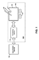
- FIG. 1 is a block diagram of an exemplary input device 100 , in accordance with embodiments.
- Input device 100 may be configured to provide input to an electronic system (not shown).
- electronic system broadly refers to any system capable of electronically processing information.
- electronic systems include personal computers of all sizes and shapes, such as desktop computers, laptop computers, netbook computers, tablets, web browsers, e-book readers, and personal digital assistants (PDAs).
- PDAs personal digital assistants
- Additional example electronic systems include composite input devices, such as physical keyboards that include input device 100 and separate joysticks or key switches.
- peripherals such as data input devices (including remote controls and mice), and data output devices (including display screens and printers).
- Other examples include remote terminals, kiosks, and video game machines (e.g., video game consoles, portable gaming devices, and the like).
- Other examples include communication devices (including cellular phones, such as smart phones), and media devices (including recorders, editors, and players such as televisions, set-top boxes, music players, digital photo frames, and digital cameras).
- the electronic system could be a host or a slave to the input device.
- Input device 100 can be implemented as a physical part of the electronic system, or can be physically separate from the electronic system. As appropriate, input device 100 may communicate with parts of the electronic system using any one or more of the following: buses, networks, and other wired or wireless interconnections. Examples include, but are not limited to: Inter-Integrated Circuit (I2C), Serial Peripheral Interface (SPI), Personal System 2 (PS/2), Universal Serial Bus (USB), Bluetooth®, Radio Frequency (RF), and Infrared Data Association (IrDA).
- I2C Inter-Integrated Circuit
- SPI Serial Peripheral Interface
- PS/2 Personal System 2
- USB Universal Serial Bus
- Bluetooth® Radio Frequency
- RF Radio Frequency
- IrDA Infrared Data Association
- input device 100 is shown as a proximity sensor device (also often referred to as a “touchpad” or a “touch sensor device”) configured to sense input provided by one or more input objects 140 in a sensing region 120 .
- Example input objects include fingers and styli, as shown in FIG. 1 .
- Sensing region 120 encompasses any space above, around, in and/or near the input device 100 in which the input device 100 is able to detect user input (e.g., user input provided by one or more input objects 140 ).
- the sizes, shapes, and locations of particular sensing regions may vary widely from embodiment to embodiment.
- sensing region 120 extends from a surface of input device 100 in one or more directions into space until signal-to-noise ratios prevent sufficiently accurate object detection.
- the distance to which this sensing region 120 extends in a particular direction in various embodiments, may be on the order of less than a millimeter, millimeters, centimeters, or more, and may vary significantly with the type of sensing technology used and the accuracy desired.
- some embodiments sense input that comprises no contact with any surfaces of input device 100 , contact with an input surface (e.g., a touch surface) of the input device 100 , contact with an input surface of input device 100 coupled with some amount of applied force or pressure, and/or a combination thereof.
- input surfaces may be provided by surfaces of casings within which the sensor electrodes reside, by face sheets applied over the sensor electrodes or any casings, etc.
- sensing region 120 has a rectangular shape when projected onto an input surface of input device 100 .
- Input device 100 may utilize any combination of sensor components and sensing technologies to detect user input in the sensing region 120 .
- Input device 100 comprises one or more sensing elements for detecting user input.
- input device 100 may use capacitive techniques.
- Some implementations are configured to provide images that span one, two, three, or higher dimensional spaces. Some implementations are configured to provide projections of input along particular axes or planes.
- voltage or current is applied to create an electric field. Nearby input objects cause changes in the electric field, and produce detectable changes in capacitive coupling that may be detected as changes in voltage, current, or the like.
- Some capacitive implementations utilize arrays or other regular or irregular patterns of capacitive sensing elements to create electric fields.
- separate sensing elements may be ohmically shorted together to form larger sensor electrodes.
- Some capacitive implementations utilize resistive sheets, which may be uniformly resistive.
- Some capacitive implementations utilize “self capacitance” (or “absolute capacitance”) sensing methods based on changes in the capacitive coupling between sensor electrodes and an input object.
- an input object near the sensor electrodes alters the electric field near the sensor electrodes, thus changing the measured capacitive coupling.
- an absolute capacitance sensing method operates by modulating sensor electrodes with respect to a reference voltage (e.g., system ground), and by detecting the capacitive coupling between the sensor electrodes and input objects.
- Some capacitive implementations utilize “mutual capacitance” (or “transcapacitance”) sensing methods based on changes in the capacitive coupling between sensor electrodes.
- an input object near the sensor electrodes alters the electric field between the sensor electrodes, thus changing the measured capacitive coupling.
- a transcapacitive sensing method operates by detecting the capacitive coupling between one or more transmitter sensor electrodes (also “transmitter electrodes” or “transmitters”) and one or more receiver sensor electrodes (also “receiver electrodes” or “receivers”).
- transmitters and receivers may be referred to as sensor electrodes or sensor elements.
- Transmitter sensor electrodes may be modulated relative to a reference voltage (e.g., system ground) to transmit transmitter signals. Receiver sensor electrodes may be held substantially constant relative to the reference voltage to facilitate receipt of resulting signals.
- a resulting signal may comprise effect(s) corresponding to one or more transmitter signals, and/or to one or more sources of environmental interference (e.g., other electromagnetic signals).
- Sensor electrodes may be dedicated transmitters or receivers, or may be configured to both transmit and receive.
- one or more receiver electrodes may be operated to receive a resulting signal when no transmitter electrodes are transmitting (e.g., the transmitters are disabled). In this manner, the resulting signal represents noise detected in the operating environment of sensing region 120 .
- a processing system 110 is shown as part of input device 100 .
- the processing system 110 is configured to operate the hardware of input device 100 to detect input in the sensing region 120 .
- Processing system 110 comprises parts of or all of one or more integrated circuits (ICs) and/or other circuitry components.
- ICs integrated circuits
- processing system 110 also comprises electronically-readable instructions, such as firmware code, software code, and/or the like.
- components composing processing system 110 are located together, such as near sensing element(s) of input device 100 .
- components of processing system 110 are physically separate with one or more components close to sensing element(s) of input device 100 , and one or more components elsewhere.
- input device 100 may be a peripheral coupled to a desktop computer, and processing system 110 may comprise software configured to run on a central processing unit of the desktop computer and one or more ICs (perhaps with associated firmware) separate from the central processing unit.
- input device 100 may be physically integrated in a phone, and processing system 110 may comprise circuits and firmware that are part of a main processor of the phone.
- processing system 110 is dedicated to implementing input device 100 .
- processing system 110 also performs other functions, such as operating display screens, driving haptic actuators, etc.
- Processing system 110 may be implemented as a set of modules that handle different functions of processing system 110 .
- Each module may comprise circuitry that is a part of processing system 110 , firmware, software, or a combination thereof.
- Example modules include hardware operation modules for operating hardware such as sensor electrodes and display screens, data processing modules for processing data such as sensor signals and positional information, and reporting modules for reporting information.
- Further example modules include sensor operation modules configured to operate sensing element(s) to detect input, identification modules configured to identify gestures such as mode changing gestures, and mode changing modules for changing operation modes.
- processing system 110 responds to user input (or lack of user input) in sensing region 120 directly by causing one or more actions.
- Example actions include changing operation modes, as well as GUI actions such as cursor movement, selection, menu navigation, and other functions.
- processing system 110 provides information about the input (or lack of input) to some part of the electronic system (e.g., to a central processing system of the electronic system that is separate from processing system 110 , if such a separate central processing system exists).
- some part of the electronic system processes information received from processing system 110 to act on user input, such as to facilitate a full range of actions, including mode changing actions and GUI actions.
- processing system 110 operates the sensing element(s) of input device 100 to produce electrical signals indicative of input (or lack of input) in sensing region 120 .
- Processing system 110 may perform any appropriate amount of processing on the electrical signals in producing the information provided to the electronic system.
- processing system 110 may digitize analog electrical signals obtained from the sensor electrodes.
- processing system 110 may perform filtering or other signal conditioning.
- processing system 110 may subtract or otherwise account for a baseline, such that the information reflects a difference between the electrical signals and the baseline.
- processing system 110 may determine positional information, recognize inputs as commands, recognize handwriting, and the like.
- Positional information as used herein broadly encompasses absolute position, relative position, velocity, acceleration, and other types of spatial information.
- Exemplary “zero-dimensional” positional information includes near/far or contact/no contact information.
- Exemplary “one-dimensional” positional information includes positions along an axis.
- Exemplary “two-dimensional” positional information includes motions in a plane.
- Exemplary “three-dimensional” positional information includes instantaneous or average velocities in space. Further examples include other representations of spatial information.
- Historical data regarding one or more types of positional information may also be determined and/or stored, including, for example, historical data that tracks position, motion, or instantaneous velocity over time.
- input device 100 is implemented with additional input components that are operated by processing system 110 or by some other processing system. These additional input components may provide redundant functionality for input in sensing region 120 , or some other functionality.
- FIG. 1 shows buttons 130 near sensing region 120 that can be used to facilitate selection of items using input device 100 .
- Other types of additional input components include sliders, balls, wheels, switches, and the like.
- input device 100 may be implemented with no other input components.
- input device 100 may be a touch screen, and sensing region 120 overlaps at least part of an active area of a display screen 160 .
- the input device 100 may comprise substantially transparent sensor electrodes overlaying the display screen 160 and provide a touch screen for the associated electronic system.
- the display screen 160 may be any type of dynamic display capable of displaying a visual interface to user, and may include any type of light emitting diode (LED), organic LED (OLED), cathode ray tube (CRT), liquid crystal display (LCD), plasma, electroluminescence (EL), or other display technology.
- the input device 100 and the display screen 160 may share physical elements.
- some embodiments may utilize some of the same electrical components for displaying and sensing.
- the display screen 160 may be operated in part or in total by processing system 110 .
- the mechanisms are capable of being distributed as a program product (e.g., software) in a variety of forms.
- the mechanisms that are described may be implemented and distributed as a software program on information bearing media that are readable by electronic processors (e.g., non-transitory computer-readable and/or recordable/writable information bearing media readable by processing system 110 ).
- the embodiments apply equally regardless of the particular type of medium used to carry out the distribution. Examples of non-transitory, electronically readable media include various discs, memory sticks, memory cards, memory modules, and the like.
- Electronically readable media may be based on flash, optical, magnetic, holographic, or any other tangible storage technology.
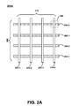
- FIG. 2A shows a portion of an example sensor electrode pattern 200 A which may be utilized in a sensor to generate all or part of the sensing region of a input device 100 , according to various embodiments.
- Input device 100 is configured as a capacitive input device when utilized with a capacitive sensor electrode pattern.
- a non-limiting simple rectangular sensor electrode pattern 200 A is illustrated. It is appreciated that numerous other sensor electrode patterns may be employed.
- the illustrated sensor electrode pattern is made up of a plurality of receiver electrodes 270 ( 270 - 0 , 270 - 1 , 270 - 2 . . .
- Capacitive pixel 290 illustrates one of the capacitive pixels generated by sensor electrode pattern 200 A. It is appreciated that in a crossing sensor electrode pattern, such as the illustrated example, some form of insulating material or substrate is typically disposed between transmitter electrodes 260 and receiver electrodes 270 .
- transmitter electrodes 260 and receiver electrodes 270 may be disposed on the same layer as one another through use of routing techniques and/or jumpers.
- a plurality of receiver electrodes 270 and/or a plurality of transmitter electrodes 260 may be formed of various shapes, such as pronged or tined electrodes, U-shaped electrodes or electrode elements having unique shapes (e.g., H or I shaped electrode elements).
- touch sensing includes sensing input objects anywhere in sensing region 120 and may comprise: no contact with any surfaces of the input device 100 , contact with an input surface (e.g., a touch surface) of the input device 100 , contact with an input surface of the input device 100 coupled with some amount of applied force or pressure, and/or a combination thereof.
- an input surface e.g., a touch surface
- Capacitive pixels such as capacitive pixel 290 are areas of localized capacitive coupling between transmitter electrodes 260 and receiver electrodes 270 .
- the capacitive coupling between transmitter electrodes 260 and receiver electrodes 270 changes with the proximity and motion of input objects in the sensing region associated with transmitter electrodes 260 and receiver electrodes 270 .
- sensor electrode pattern 200 A is “scanned” to determine these capacitive couplings. That is, the transmitter electrodes 260 are driven to transmit transmitter signals. Transmitters may be operated such that one transmitter electrode transmits at one time, or multiple transmitter electrodes transmit at the same time. Where multiple transmitter electrodes transmit simultaneously, these multiple transmitter electrodes may transmit the same transmitter signal and produce an effectively larger transmitter electrode, or these multiple transmitter electrodes may transmit different transmitter signals. For example, multiple transmitter electrodes may transmit different transmitter signals according to one or more coding schemes that enable their combined effects on the resulting signals of receiver electrodes 270 to be independently determined.
- the receiver electrodes 270 may be operated singly or multiply to acquire resulting signals.
- the resulting signals may be used to determine measurements of the capacitive couplings at the capacitive pixels.
- a set of measurements from the capacitive pixels form a “capacitive image” (also “capacitive frame”) representative of the capacitive couplings at the pixels.
- Capacitive image also “capacitive frame”
- Multiple capacitive images may be acquired over multiple time periods, and differences between them used to derive information about input in the sensing region. For example, successive capacitive images acquired over successive periods of time can be used to track the motion(s) of one or more input objects entering, exiting, and within the sensing region.
- the baseline capacitance of a sensor device is the capacitive image associated with no input object in the sensing region.
- the baseline capacitance changes with the environment and operating conditions, and may be estimated in various ways. For example, some embodiments take “baseline images” when no input object is determined to be in the sensing region, and use those baseline images as estimates of their baseline capacitances.
- Capacitive images can be adjusted for the baseline capacitance of the sensor device for more efficient processing. Some embodiments accomplish this by “baselining” measurements of the capacitive couplings at the capacitive pixels to produce a “baselined capacitive image.” That is, some embodiments compare the measurements forming a capacitance image with appropriate “baseline values” of a “baseline image” associated with those pixels, and determine changes from that baseline image.
- some embodiments are configured to measure environmental interference (e.g., ambient noise) during a time when no transmitter signals are being transmitted. In this way, resulting signals received by the receiver electrodes would not contain any effects due to the transmitter signals.
- environmental interference e.g., ambient noise
- FIG. 2B shows an input device comprising a sensor electrode pattern which includes a plurality of common electrodes, and which may be utilized in a sensor to generate all or part of the sensing region of an input device, such as a touch screen, according to some embodiments.
- FIG. 2B shows input device 100 B with a sensor electrode pattern 200 B (comprising common electrodes 260 and receiver electrodes 270 ), and a processing system 110 (illustrated in two portions, 110 - 1 and 110 - 2 ).
- processing system portion 110 - 1 is coupled with receiver electrodes 270 and configured to receive resulting signals from receiver electrodes 270 .
- Processing system portion 110 - 2 is coupled with common electrodes 260 , and comprises display circuitry (not shown) configured for displaying images on a combination display screen/touch screen 160 / 100 which may be referred to herein as an “integrated touch screen.”
- the display circuitry is configured to apply one or more pixel voltage(s) to the display pixel electrodes through pixel source drivers (not shown).
- the display circuitry is also configured to apply one or more common drive voltage(s) to the common electrodes 260 , and operate them as V-com electrodes of the display screen portion of the integrated touch screen.
- the display circuitry is also configured to invert the common drive voltage in synchronization with a drive cycle of the image display upon the display screen portion.
- the processing system portion 110 - 2 is also configured to operate common electrodes 260 as transmitter electrodes for capacitive sensing on the touch screen portion of integrated touch screen.
- the processing system for the device comprises two separate portions 110 - 1 and 110 - 2 .
- the processing system may be implemented as more or fewer portions.
- the functions of the processing system portion 110 - 1 and the processing system portion 110 - 2 may be implemented as one integrated circuitry. Synchronization between separate processing system portions 110 - 1 , 110 - 2 , etc., may be achieved by communicating between portions with synchronization mechanism 291 .
- synchronization mechanism 291 may synchronize display updating and capacitive sensing by providing a synchronized clock, information about display update state, information about the capacitive sensing state, direction to display circuitry to update (or not to update), direction to capacitive sensing circuitry to sense (or not to sense), and/or the like.
- the common electrodes transmit signals for display updating and capacitive sensing in the same time period, or in different time periods.
- the common electrodes may transmit signals for display updating during a display-update time of a row update cycle, and transmit signals for capacitive sensing during a non-display time of the row update cycle (e.g., sometimes called “horizontal blanking time”).
- the common electrodes may transmit signals for display updating during row update cycles with actual display row updates, and transmit signals for capacitive sensing during extra “row update cycles” without actual display row updates (e.g., the non-display times between updating sections of frames or entire frames, sometimes called “vertical blanking time”).
- the common electrodes may transmit signals simultaneously for display updating and capacitive sensing, but separate them spatially.
- the common electrodes may use the same transmission for both display updating and capacitive sensing.
- other components are shared in addition (or in place of) common electrodes.
- one processing system may be used to perform both capacitive sensing and display updating functions.
- Some embodiments are configured to measure environmental interference (e.g., ambient noise) during a time when no transmitter signals are being transmitted. In this way, resulting signals received by the receiver electrodes would not contain any effects due to the transmitter signals.
- environmental interference e.g., ambient noise
- Some touch screen embodiments also synchronize environmental interference detection with display screen operation, such that interference caused by display screen operation is avoided in part or in whole, is anticipated and accommodated in some other manner (e.g., operating at an unlike frequency or phase, filtering, etc.), and/or the like.
- Some touch screen embodiments with synchronized capacitive sensing and display updating are configured to detect environmental interference without changing the synchronization between display updating and capacitive sensing or disturbing the display updating sequence.
- some embodiments with common electrodes are configured to detect environmental interference by not driving the common electrodes to update the display or to transmit transmitter signals for capacitive sensing during a non-display time (e.g., horizontal blanking time, vertical blanking time).
- a non-display time e.g., horizontal blanking time, vertical blanking time.
- These embodiments may or may not sense input objects during another non-display time (e.g., vertical blanking time or another part of the horizontal blanking time if the embodiment senses interference during the horizontal blanking time, horizontal blanking time or another part of the vertical blanking time if the embodiment senses interference during the vertical blanking time).
- some embodiments are configured to detect environmental interference and not sense input objects during for one or more parts of a capacitive frame period, or even for an entire capacitive frame period, while display updating proceeds as usual.
- capacitive frame period is used to indicate the time period allotted for capacitive sensing, which usually corresponds with when a capacitive image is acquired (or would have been acquired if not measuring interference).
- the embodiments which detect interference for part of a capacitive frame period may or may not perform any input object detecting during another part of that same capacitive frame period. Where input object detection is performed, it may be to the same or a lower resolution than that of a frame without interference detection.
- some such embodiments may be configured to detect presence/no presence of input objects in the sensing region, or to detect positional information to a coarser resolution.
- Some touch screen embodiments with synchronized capacitive sensing and display updating are configured to detect environmental interference in a way that does change the display updating sequence. For example, some embodiments are configured to pause display updating while sensing interference. After interference has been sensed, display updating restarts.
- some embodiments detect interference by pausing the capacitive scanning associated with input object detection while continuing to update the display. This approach may change the synchronization of the capacitive sensing and the display updating. To accommodate these changes, these embodiments may be configured to track the relationship between the capacitive scanning associated with input object detection and the display updating, map portions of different frame types to portions of the capacitive measurements, and adjust the capacitive measurements appropriately. (“Frame type” is discussed further below in conjunction with FIGS. 7A-7F and 8 A- 8 F.)
- Some touch screens and/or input devices in accordance with various embodiments operate according to a method comprising: operating in an interference sensing state and separately operating in an input object sensing sate. While sensing interference in the interference sensing state, the touch screen/input device may not transmit transmitter signals. While sensing input objects in the input object sensing state, the touch screen/input device does transmit transmitter signals.
- the interference sensing state and the input object sensing state may each have any appropriate duration.
- a touch screen/input device may be in the interference sensing state (or the input object sensing state) for a portion of a capacitive frame, or last for many capacitive frames, before switching out of that state.
- a touch screen/input device may be in the interference sensing state (or the input object sensing state) until one or more criteria are met.
- Example criteria include interference level detected, the presence (or lack of presence) of input objects, the type of input detected, etc.
- Some touch screens/input devices in accordance with various embodiments operate according to a method that further comprises: operating in an interference avoidance state, wherein one or more interference avoidance actions is taken.
- the interference avoidance state may similarly last any appropriate duration.
- some touch screens/input devices may operate with interference avoidance states that occur between capacitive frames, for one or more portions of one or more capacitive frames, or for one or more entire capacitive frames.
- FIG. 3 illustrates a block diagram of some components of an example processing system 110 A that may be utilized with an input device (e.g., in place of processing system 110 as part of input device 100 ), according to various embodiments.
- Processing system 110 A may be implemented with one or more Application Specific Integrated Circuits (ASICSs), one or more Integrated Circuits (ICs), one or more controllers, or some combination thereof.
- ASICSs Application Specific Integrated Circuits
- ICs Integrated Circuits
- processing system 110 A is communicatively coupled with one or more transmitter electrode(s) and receiver electrode(s) that implement a sensing region 120 of an input device 100 .
- processing system 110 A and the input device 100 may be disposed in or communicatively coupled with an electronic device 150 , such as a display device, computer, or other electronic device.
- an electronic device 150 such as a display device, computer, or other electronic device.
- processing system 110 A includes, among other components: sensor circuitry 310 , control logic 320 , and display circuitry 330 .
- Processing system 110 A and/or components thereof may be coupled with sensor electrodes of a sensor electrode pattern, such as sensor electrode pattern 200 ( 200 A, 200 B).
- sensor circuitry 310 is coupled with one or more sensor electrodes of a sensor electrode pattern (e.g., sensor electrode pattern 200 A, 200 B, or the like).
- Sensor circuitry 310 operates to interact with receiver and transmitter sensor electrodes of a sensor pattern that is utilized to generate a sensing region 120 . This includes operating transmitter electrodes to be “silent” (e.g., not transmitting a received transmitter signal) or transmit a transmitter signal. This also includes utilizing receiver sensor electrodes to receive resulting signals and other signals which may be interference. Sensor circuitry 310 may also determine from received resulting signal(s) that an input has occurred in sensing region 120 , as well as determining a location of the input with respect to sensing region 120 . Sensor circuitry 310 may further determine that interference is occurring and/or determine the nature of the interference. As depicted in FIG. 3 , sensor circuitry 310 may include one or more of transmitter circuitry 311 , receiver circuitry 312 , computation circuitry 313 , and interference measurement circuitry 314 .
- Transmitter circuitry 311 operates to transmit received transmitter signals on one or more transmitter electrodes 260 .
- transmitter circuitry 311 may transmit or not transmit a transmitter signal (waveform) on one or more of a plurality of transmitter electrodes 260 .
- Transmitter circuitry 311 may also be utilized to couple one or more transmitter electrodes 260 (and respective transmitter path(s)) of a plurality of transmitter electrodes 260 to high impedance, ground, or to a constant voltage when not transmitting a waveform on such transmitter electrodes.
- the transmitter signal may be a square wave, trapezoidal wave, or some other waveform.
- Transmitter circuitry 311 may code a transmitter signal, such as in a code division multiplexing scheme.
- the code may be altered, such as lengthening or shortening the code, under direction of control logic 320 . Lengthening the code is one technique for avoiding interference.
- the waveforms of the transmitter signal may be of different frequency, phase, or amplitude. Code divisions may be temporally or spatially divided.
- Receiver circuitry 312 operates to receive resulting signals, via receiver electrodes.
- the received resulting signals correspond to and include some version of the transmitter signal(s) transmitted via the transmitter electrodes.
- These transmitted transmitter signals may be altered or changed in the resulting signal due to stray capacitance, noise, interference, and/or circuit imperfections among other factors, and thus may differ slightly or greatly from their transmitted versions.
- receiver circuitry 312 may be equipped to implement one or more filtering operations, which may include utilizing either or both of linear and non-linear filtering techniques.
- the filters may be analog or digital.
- Some non-limiting examples of filters include: low pass filters/demodulators, finite impulse response (FIR) filters, and infinite impulse response (IIR) filters.
- filtering operations may be implemented, not implemented, and/or modified under direction of control logic 320 .
- Resulting signals may be received on one or a plurality of receiver electrodes during a time interval.
- Receiver circuitry 312 includes a plurality of amplifiers, typically one per receiver electrode. Such amplifiers may be referred to herein as amplifiers, front-end amplifiers, integrating amplifiers, or the like, and receive a reference voltage at a first input and a resulting signal at a second input. The resulting signal is from a receiver electrode of a capacitive sensor device.
- Computation circuitry 313 operates to compute/determine a measurement of a change in a capacitive coupling between a transmitter electrode and a receiver electrode. Computation circuitry then uses this measurement to determine the position of an input object (if any) with respect to sensing region 120 . Computation circuitry 313 can provide an indication of the quality of a resulting signal. For example looking at the reported position of an input object to determine if it is representative of an intended user action; thus a reported position which appears to “jitter” or otherwise replicate an unrealistic user input can be an indication of interference in a resulting signal received and interference avoidance actions can be implemented. Computation circuitry 313 can further produce a confidence indication as to the quality of demodulated signal.
- Interference measurement circuitry 314 operates to measure when and to what extent interference is occurring. This can comprise actively sensing for and measuring interference using receiver sensor electrodes or sensing the effects of interference. Such sensing may be accomplished with one, some, or a combination of all receiver sensor electrodes. Active sensing for and measuring of interference can occur when one or more transmitter electrodes are transmitting or can occur when transmitter electrodes are not transmitting (this can include simply not transmitting or additionally being coupled to a high impedance). Typically, such active sensing for and measuring interference takes up time that might otherwise be used for sensing for an actual input from an input object.
- Effects which indicate interference is occurring include difficulty or impossibility of receiver circuitry 312 sensing a resulting signal when transmitter electrodes are transmitting (e.g., clipping), and receiver circuitry 312 experiencing corruption of a received resulting signal (e.g., interference typical of a known noise source, or calculated position/motion atypical of user input such as an input object appearing to jump back and forth quickly in the sensing region). While the transmitter electrodes may be “off” or “silent” with respect to transmitting signals for capacitive sensing, they may transmit other signals not used for capacitive sensing.
- the transmitter electrodes may transmit signals that cannot be picked up by the receiver electrodes, such signals are those that are out of band with the frequency band tracked by the receiver electrode, on a substantially orthogonal code, or below a threshold that is sensed.
- the transmitter electrodes may be utilized to transmit shield or ground signals or may be transmitting RFID or other communications signals that have nothing to do with capacitive sensing signals that can be received with the receiver electrodes.
- Certain aspects of signals received by receiver electrodes can be analyzed to determine if there is an interferer present when a transmitter is active. For example, one or a combination of the power, peak amplitude, or spectrum of a received signal (in response to transmitting a transmitter signal) can be analyzed.
- the presence of interference can be determined and it can be determined if the interference is within or outside of an acceptable bound for capacitive input sensing.
- interference when interference is measured during periods when the transmitter electrodes are not being driven by a transmitter signal (for capacitive sensing purposes), interference can be measured and analyzed directly from the receiver signal which would otherwise be quiet in the absence of interference. Many of the types of effects of interference can be measured passively.
- Interference measurement circuitry 314 may communicate information about interference determinations to control logic 320 and, under direction of control logic 320 , may also alter one or more aspects of how measuring interference and resulting signals takes place. Alternately, linear or non-linear filters based on interference models or a user input usage model may be applied to the capacitance image, the position reporting, or intermediate representations based on one or more measurements of interference.
- Control logic 320 comprises decision making logic which directs processing system 110 A and sensor circuitry 310 to operate in a selected one of a plurality of different operating modes based on various inputs. Some non-limiting examples of such inputs include one or more measurement(s) of interference and/or indication of an input being sensed or not sensed in sensing region 120 of input device 100 .
- Control logic may be implemented as hardware (e.g., hardware logic and/or other circuitry) and/or as a combination of hardware and instructions stored in a non-transitory manner in a computer readable storage medium.
- Display circuitry 330 when included, displays images on a combination display screen/touch screen (e.g., 160 / 100 of FIGS. 1 , 2 A, and 2 B) that may be referred to herein as an integrated touch screen.
- Display circuitry 330 applies one or more pixel voltage(s) or current(s) to the display pixel electrodes through pixel source drivers (not shown).
- Display circuitry 330 applies one or more common drive voltage(s) to the common electrodes (e.g., common electrodes 260 ), and operates them as V-com electrodes of the display screen portion of the integrated touch screen.
- display circuitry 330 inverts the common drive voltage in synchronization with a drive cycle of the image display (e.g., 160 ) upon the display screen of an integrated touch screen.
- a capacitive input device such as a touch screen
- noise interference that is present without a finger (or other object) touching or otherwise in proximity to the capacitive input device in the input region
- noise interference that is only present when a finger (or other object) is touching or otherwise in proximity to the input device in the input region.
- the first case is associated with noise interference from electronic devices in proximity to the capacitive input device.
- noise interference from electronic devices in proximity to the capacitive input device.
- back-coupled noise from an LCD underneath a sensor electrode pattern or disposed in conjunction with a sensor electrode pattern is a common source of noise interference.
- Such interference sources are often stationary in the sense that their frequency components are fairly constant over time.
- the second case can arise when noise interference in the environment of the input device is coupled into the sensor from an input object. This is often referred to as “input object coupled interference.”
- the second case can also happen when interference from a power supply charger causes the potential of a sensor electrode pattern (or one or more sensors thereof) to vary with respect to earth ground and an input object which is coupled to earth ground touches the input device.
- the conventional strategy is to try to quickly detect input object coupled interference and respond appropriately.
- observation number two suggests that if there is an interferer it will be present when the input object first touches the input device in the sensing region. The converse is also true: if the interference is not present when the input object first touches the input device in the sensing region, typically it will not spontaneously appear during the time the input object remains in contact within the sensing region of the input device.
- FIG. 4 shows a flow chart 400 for an example method of operating a capacitive input device that is configured to sense in a sensing region, according to various embodiments.
- noise detection will not suffer from false positives induced from input object signals, nor will the frame rate or signal to noise ration suffer from dedicating a portion of normal frame processing to noise processing.
- the transmitters are not transmitting transmitter signals, and interference is sensed.
- control logic 320 may instruct transmitter circuitry 311 not to transmit on transmitters (e.g., transmitter electrodes 260 ) of capacitive input device 100 .
- transmitters e.g., transmitter electrodes 260
- the receivers of capacitive input device 100 can be used to sense any interference that is present.
- the transmitter electrodes 260 are common electrodes utilized in both a touch screen and a display device
- the interference is sensed during a non-display update time so that that no transmissions, for either sensing or display updating, will be taking place with the common electrodes.
- control logic 320 determines if the interference is within appropriate parameters or outside of appropriate parameters (e.g., is there too much interference for effective input object sensing). For example, control logic 320 determines if an interference condition indicative of the interference being within acceptable bounds has been met. This determination can be made in various manners, such as by comparison with one or more interference thresholds, analysis of various heuristics and or analysis of spectrums or histograms associated with the interference, and/or other technique(s). If the interference condition is not met, then interference is deemed outside of bounds for acceptable conduct of input sensing.
- the determination by control logic 320 as to whether or not an interference condition has been met additionally or alternatively may involve one or more of detecting the power associated with the interference using a power detector (such as a square-law detector), filtering the interference signal (such as with a sum of absolute differences), or other interference determining techniques.
- a power detector such as a square-law detector
- filtering the interference signal such as with a sum of absolute differences
- control logic 320 instructs sensor circuitry 310 to perform one or more interference avoidance actions in procedure 430 and the system returns to procedure 410 after the interference avoidance action(s) have been performed.
- Some non-limiting examples of corrective actions that may be taken in procedure 430 include changing a sensing frequency, changing an order of filters applied, changing the frequency response(s) of the filter(s) used, lowering the report frame rate, changing a code or a code length of a transmitter signal, etc.
- the system proceeds to sense input objects in procedure 440 after performing interference avoidance actions in procedure 430 .
- control logic 320 instructs transmitter circuitry 311 to transmit transmitter signals and the capacitive input device 100 scans for input(s) in sensing region in procedure 440 .
- Computation circuitry 313 determines if an input from an input object has been detected in procedure 450 . This determination can be accomplished in any appropriate way. For example, processing system 110 A may use only the signals just acquired in procedure 440 , use the signals just acquired in procedure 440 along with signals acquired in earlier performances of procedure 440 , use signals 400 along with signals acquired earlier in performances of procedure 410 , etc. As another example, the computation circuitry 313 of processing system 110 A may use some or all of the signals acquired in any performance of procedure 440 . If one or more inputs are detected, then the processing system 110 A loops back to procedure 440 . In one embodiment, when no input(s) are detected, then processing system 110 A returns from procedure 450 to procedure 410 . This is illustrated in flow chart 400 by the return loop between procedure 450 and procedure 410 that occurs in response to an input object not being detected.
- Embodiments may also have different ordering of the procedures. For example, some embodiments may be configured to sense input from input objects before finishing a determination of whether the interference condition is within an acceptable bound. In such a case, the scanning for input objects may occur in parallel with processing for evaluating the amount of interference, and procedures such as taking an interference avoidance action may be linked differently with other procedures.
- interference sensing may be interleaved with sensing cycles. In some embodiments, some interference sensing may be performed during procedure 440 , however such sensing is accomplished at a lower fidelity that the interference sensing which is accomplished in procedure 410 .
- some lower fidelity interference sensing may be accomplished and then procedure 440 repeated without moving on to procedure 450 .
- Some interference avoidance actions e.g., applying filtering
- Some embodiment may be configured to perform interference avoidance actions 430 while an input object is detected during input object detection 440 .
- Some embodiments may be configured to sense interference during a non-display update time 410 while an input object is detected during input object detection 440 .
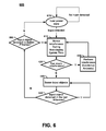
- FIG. 5 shows a flow chart 500 for an example method of operating a capacitive input device that is configured to sense in a sensing region, according to various embodiments.
- Flow chart 500 illustrates a variation on the method illustrated in flow chart 400 .
- flow chart 500 illustrates detection of an input object (in procedure 550 ) based on the last N frames.
- Procedures 410 - 440 of flow chart 500 are analogous to procedures 410 - 440 of flow chart 400
- procedure 550 is a variation of procedure 450
- Procedure 550 varies from procedure 450 by being configured to determine if an input associated with an input object was sensed in sensing region 120 for the last frame acquired, for a selected number of frames acquired, for the last N frames acquired, within a certain time period, etc. In one embodiment, when no input(s) are detected in the last N frames, then processing system 110 A returns from procedure 550 to procedure 410 . This is illustrated in flow chart 500 by the return loop between procedure 550 and procedure 410 that occurs in response to an input object not being detected in the last N frames. In one embodiment, control logic 320 makes the determination.
- transition from procedure 550 to procedure 410 is generally more immediate and very similar to the change between procedures 450 and 410 of flow chart 400 .
- determination is based on history (e.g., a longer time period; select frames from a time period prior to the current time; or including or not including the most recent sample, such as the last N frames where N>1)
- processing system 110 A generally changes from procedure 550 to procedure 410 more slowly than the change from procedure 450 to procedure 410 .
- the change is slower because processing system 110 A generally does not immediately start sensing interference in response to a determination of no input objects in the sensing region 120 . Both approaches have advantages.
- processing systems 100 A with input object detection periods in procedure 550 that are based on history may be more efficient in sensing and processing some gestures involving multiple sequential taps by input objects, as noise detection does not immediately begin after an input object is lifted. For example, fast finger taps are processed more efficiently after the first tap is detected if N>1.
- some embodiments are configured to sense interference even if input object(s) are detected in the sensing region, at a slower rate than if no input object(s) are detected in the sensing region. For example, some embodiments are configured to sense interference every M frames when input object(s) are detected in the sensing region. As a further example, some embodiments are configured to sense interference in response to a determination that the input object data acquired meets or does not meet some criteria or additional interference condition (e.g., received resulting signals appear corrupted because of a heuristic model, such as a calculated input object position being outside of an expected usage model, or sensor circuitry detecting non-linearity conditions with the receiver(s)).
- some criteria or additional interference condition e.g., received resulting signals appear corrupted because of a heuristic model, such as a calculated input object position being outside of an expected usage model, or sensor circuitry detecting non-linearity conditions with the receiver(s)).
- Heuristic models may be based on either the total image or the portion of the image near where an input object is sensed.
- various embodiments may sense interference if the input(s) detected in the sensing region are determined to have changed (e.g., input(s) not in contact with the input surface, hovering above the input surface, and/or added and/or removed from the sensing region).
- timing there is a choice for how to implement the timing of the sensing of procedures 410 and 440 .
- One option is to choose timing so that procedure 440 has the desired frame rate when an input object is present but additional time is allowed for noise detection when no input object is present. In this case there will be a slight increase in latency in detecting an input object. For instance, if the input object processing frame rate is 100 Hz and an additional 25% of time is spent on noise detection, then the input object detection latency can increase by 2.5 mS. However, once an input object is detected, the frame rate reaches its full rate. In the second case a lesser amount of time is spent in procedure 440 when no input object is present such that the frame rate is the same whether or not noise detection is active. In this case there might be a slight decrease in position accuracy for the initial input object position and some complications can be incurred because the filter settling will be different in the sensing carried out in procedures 410 and 440 .
- FIG. 6 shows a flow chart 600 for an example method of operating a capacitive input device that is configured to sense in a sensing region, according to various embodiments.
- Flow chart 600 illustrates some example variations and adaptations on the method illustrated in flow chart 500 .
- procedures 410 - 440 and 550 are analogous to procedures 410 - 440 and 550 of flow chart 500 .
- control logic 320 checks in procedure 660 if P frames have passed since input objects have moved or have been removed (where P is greater or equal to N).
- control logic 320 returns processing system 110 A to procedure 410 and directs processing system 110 A to sense interference. If no input has been detected in the last P frames, then control logic 320 causes processing system 110 A and input device 100 to enter a low power state in procedure 670 (e.g., a sleep mode where power utilized by capacitive input device 100 is lower than in normal operation of capacitive input device 100 ). In this low power state, processing system 110 A may be configured by control logic 320 to periodically sense for input in sensing region 120 using any appropriate method. In response to sensing such input, control logic 320 may direct processing system 110 A to procedure 410 . Where P equals N, procedures 550 and 660 may collapse into the same procedure. A longer time (e.g., multiple or narrower bandwidth) measurement(s) of an input signal (or interference) can improve the fidelity or confidence in that measurement.
- a longer time e.g., multiple or narrower bandwidth
- Some embodiments are configured to acquire full capacitive frames at the same fidelity regardless of whether or not input from one or more input objects is determined to be in sensing region 120 . This may be done by control logic 320 directing sensor circuitry 310 to vary the frame rate. For example, if input associated with one or more input objects is detected in sensing region 120 in a previous frame (or recent history), control logic 320 directs sensor circuitry 310 to spend less or no time on sensing interference (this is in accordance with the two observations described above); thus, input device 100 senses for inputs associated with input objects at a higher capacitive frame rate.
- control logic 320 directs sensor circuitry 310 to spend more time on sensing interference, and thus input device 100 senses for input objects at a lower capacitive frame rate or in less time at a lower fidelity.
- frame rate refers to the capacitive frame rate and represents how often new object detection reports (report rate) are provided by processing system 110 A.
- Part of a frame time may be dedicated to touch sensing and part of a frame time may be dedicated to noise or interference detection.
- the confidence in the input conditions (e.g., low/no interference) may allow measurements of resulting signals and interference to be traded off to improve performance based on the calculated current interference conditions being experienced.
- control logic 320 directs sensor circuitry 310 to sense at the same capacitive frame rate regardless of if input objects are determined to be in the sensing region. This may be accomplished in various ways.
- sensor circuitry 310 is directed to acquire full capacitive frames (e.g., at full fidelity) if input(s) associated with one or more input objects is determined to be in sensing region 120 , and to acquire less than full capacitive frames (e.g., at less than full fidelity and with a reduced scan time) if no input associated with an input object is determined to be in sensing region 120 .
- control logic 320 may direct sensor circuitry 310 to spend more time per scan (at the same frame rate) if input(s) associated with one or more input objects is determined to be in sensing region 120 , and spend less time per scan if no input associated with an input object is determined to be in sensing region 120 .
- control logic 320 may increase error (e.g., reduce the amount of time for settling, number of measurements, and/or the bandwidth selected).
- error e.g., reduce the amount of time for settling, number of measurements, and/or the bandwidth selected.
- the potential for increased error due to decreased settling time is somewhat unique to the sensor electrode pattern being utilized, and thus needs to be factored in to any reduction in scan time for a particular sensor electrode pattern.
- Reduced fidelity may correspond to less spatial resolution, lower frequency selectivity, lower dynamic range, fewer measurements, reduced confidence, or the like.
- control logic 320 is configured to direct sensor circuitry 310 to change both the capacitive frame rate and the sensing fidelity in response to input associated with an input object being detected in sensing region 120 .
- Metrics such as frequency, dynamic range, and resolution can be utilized to measure a level of sensing fidelity employed.
- the “capacitive frame rate” (the rate at which successive capacitive images are acquired) may be the same or be different from that of the “display frame rate” (the rate at which the display image is updated, including refreshing the screen to redisplay the same image).
- the two rates differ, successive capacitive images are acquired at different display updating states, and the different display updating states may affect the capacitive images that are acquired. That is, display updating affects, in particular, the baseline capacitive image.
- the first and second capacitive images may differ due to differences in the baseline capacitive image associated with the display updating states, and not due to user input changes in the sensing region. This is more likely where the capacitive sensing and display updating electrodes are in close proximity to each other, or when they are shared (e.g., common electrodes).
- a capacitive image that is taken during a particular display updating state is considered to be of a particular frame type. That is, a particular frame type is associated with a mapping of a particular capacitive sensing sequence (e.g., a transmitter frame scan) with a particular display sequence (e.g., half of display lines updated).
- a particular capacitive sensing sequence e.g., a transmitter frame scan
- a particular display sequence e.g., half of display lines updated.
- a first capacitive image taken during a first display updating state (e.g., quickly scanning all the transmitter electrodes and updating the top half of the display lines) is considered to be of a first frame type
- a second capacitive image taken during a second display updating state (e.g., quickly scanning all the transmitter electrodes and updating the bottom half of the display lines) is considered to be of a second frame type
- a third capacitive image taken during a first display updating state e.g., slowly scanning the top half of the transmitter electrodes and updating the top half of the display lines
- capacitive images acquired cycle through the frame types and then repeat.
- FIGS. 7A-7F show an example of such an integrated touch screen embodiment, where the capacitive frame rate is double that of the display update frame rate.
- each of the FIGS. 7A-7F represents the operation during one row update cycle, and the set of FIGS. 7A-7F spans the time needed to update a display frame.
- the light gray, dashed horizontal lines in the display screens 710 represent common electrodes (e.g., V-com electrodes) that are being used for both display updating and capacitive sensing; these common electrodes are may be implemented in the same fashion as, and interchangeable with, transmitter electrodes 260 in FIGS. 2A and 2B .
- the bold black horizontal lines 720 ( 720 a - 720 f ) represent the common electrodes that are used during that row update cycle to update the associated row
- the gray rectangles 760 ( 760 a - 760 c ) represent the pluralities of common electrodes that are used during those row update cycles to transmit transmitter signals for capacitive sensing.
- the pluralities of common electrodes represented by a single gray rectangle 760 a , 760 b , 760 c are driven together to produce larger effective electrodes.
- a first full capacitive frame is acquired during the first half of the display update period
- a second full capacitive frame is acquired during the second half of the display update period.
- FIGS. 8A-8F show another specific example of an integrated touch screen embodiment, where the capacitive frame rate is double that of the display update frame rate.
- each of the FIGS. 8A-8F represents the operation during one row update cycle, and FIGS. 8A-8F span half of the time needed to update a display frame.
- the light gray, horizontal lines in the display screens 810 represent common electrodes (e.g., V-com electrodes) that are being used for both display updating and capacitive sensing; these common electrodes are may be implemented in the same fashion as, and interchangeable with, transmitter electrodes 260 in FIGS. 2A and 2B .
- the bold black horizontal lines 820 ( 820 a - 820 c ) represent the common electrodes that are used during that row update cycle to update the associated row
- the gray rectangles 860 860 a - 860 c ) represent the pluralities of common electrodes that are used during those row update cycles to transmit transmitter signals for capacitive sensing.
- the pluralities of common electrodes represented by a single gray rectangle 860 a - c are driven together to produce larger effective electrodes.
- the common electrodes are driven only for display updating, and half of the display is updated by the end of 8 C.
- the common electrodes are driven only for capacitive sensing, and an entire capacitive frame is acquired. Not shown are the rest of the steps where the common electrodes are again driven only for display updating for the other half of the display; and then again driven only for capacitive sensing and another capacitive frame is acquired.
- the non-display time when capacitive frames are obtained may be matched to part or all of the non-display times used to keep display line update rates substantially the same between different display frame rates (sometimes also called “blanking times.”).
- the example of FIGS. 8A-8F acquires a first full capacitive frame during the first half of the display update period, and a second full capacitive frame during the second half of the display update period.
- FIGS. 7A-7F and FIGS. 8A-8F gather the capacitive images in a “raster scan” type way. That is, the capacitive image is captured line-by-line, from top to bottom.
- other embodiments may scan the capacitive images in other ways, including scanning from the middle outwards, scanning non-adjacent sections in order, scanning multiple simultaneous independent coded sequences, or temporally independent sequences (e.g., different phase, frequency, or amplitude codes), etc.
- FIGS. 7A-7F and FIGS. 8A-8F updates the displays in a raster scan type way, and other embodiments may scan the display in other ways.
- the relationship between the capacitive image scanning and the display update scanning are periodic.
- the capacitive images taken during the first parts of display update cycles face different display operating conditions than those faced by the capacitive images taken during the second parts of display update cycles.
- the capacitive images taken during the first parts of display update cycles all face a similar set of first display operating conditions
- the capacitive images taken during the second parts of display update cycles all face a similar set of second display operating conditions.
- the capacitive images taken during the first parts of display update cycles are of a first frame type
- the capacitive images taken during the second parts of display update cycles are of a second frame type.
- the differences between different frame types cause variances in the interference measurements. In such cases, comparing interference measurements taken in different frame types to each other or applying the same criterion to interference measurements taken in different frame types lead to inaccurate gauges of interference.
- Some embodiments facing this challenge take interference measurements only in one frame type. For example, some embodiments only take interference measurements in a first frame type, and use other frame types for sensing in the sensing region, interference avoidance operations, etc. Some embodiments keep different interference measurements and criteria for the different frame types; for example, some embodiment keep separate threshold levels of acceptable interference for different frame types. Some embodiments offset, normalize, or otherwise adjust the interference measurements of different frame types to similar references and scales.
- Some touch screen embodiments are configured with the assumption that interference due to coupling with the input object is only significant when an input object is sensed in the sensing region. Thus, if an input object arrives in the sensing region without significant interference, these embodiments would operate with the assumption that no significant interference from this input object will occur for the time period that this input object remains in the sensing region.
- FIGS. 9A and 9B illustrate a flow chart 900 of example methods of operating a capacitive touch screen configured to sense in a sensing region, in accordance with various embodiments.
- flow chart 700 For purposes of illustration, during the description of flow chart 700 , reference will be made to components of input device 100 of FIG. 1 , sensor electrodes of FIGS. 2A , 2 B and 3 , components of a processing system 110 that as illustrated in FIG. 3 (and as also depicted in FIGS. 1 , 2 A and 2 B), and procedures illustrated in flow charts 400 , 500 , and 600 .
- not all of the procedures described in flow chart 900 are implemented. In some embodiments, other procedures in addition to those described may be implemented. In some embodiments, procedures described in flow chart 900 may be implemented in a different order than illustrated and/or described.
- capacitive input device 100 which may be implemented as a touch screen, is operated in a first mode.
- control logic 320 may direct sensor circuitry 310 to operate in this first mode. Operation in this first mode is described in conjunction with procedures 410 and 420 of flow charts 400 , 500 , and 600 .
- the first mode comprises interference sensing at a first level and also comprises input sensing. The interference sensing is accomplished during a non-display update time of a display (e.g., display 160 ) that is associated with the touch screen 100 .
- the first mode may comprise control logic 320 directing sensor circuitry 310 to utilize a first frame rate in which a certain portion of a frame is dedicated to interference sensing and a certain portion of a frame is dedicated to input sensing.
- control logic 320 directs that some or all of the interference sensing performed in the first mode of operation is performed with transmitter electrodes of capacitive input device 100 in a non-transmitting state.
- the transmitter electrodes are common electrodes for a touch screen/display device, the interference sensing is accomplished when they are not transmitting and thus no input sensing or display updating is taking place.
- interference avoidance actions While in this first mode of operation, if interference is sensed which does not meet an interference condition (and is thus considered too high) one or more interference avoidance actions may be implemented. Conduct of this interference avoidance while in the first mode of operation is described in procedure 430 of flow charts 400 , 500 , and 600 .
- Some non-limiting examples of interference avoidance actions which may be implemented alone or in various combinations include: modifying a sensing frequency, modifying a filtering operation, increasing a code length utilized in a code division multiplexing sensing scheme, and implementing a non-linear filtering technique. It is also possible to increase overall signal quality by lowering the effective report rate or increasing latency (e.g., narrowing the receiver bandwidth, applying Infinite Impulse Response filtering, Finite Impulse Response filtering, or Kaiser filtering).
- the capacitive input device is switched to operating in a second mode, rather than in the first mode.
- This second mode and switching to this second mode are described in procedures 420 and 440 of flow charts 400 , 500 , and 600 .
- Control logic 320 directs sensor circuitry 310 to operate in the second mode.
- the switch to the second mode occurs in response to two conditions occurring.
- the first condition is that interference measured with capacitive input device 100 while in the first mode has met an interference condition, and is thus deemed not to be within an effective range for input sensing (e.g., interference is not too high).
- the second condition is a determination that an input is in the sensing region of capacitive input device 100 .
- interference sensing with capacitive input device 100 is either not performed or else is performed at a second level that is lower in fidelity than the first level of interference sensing.
- the lower fidelity may be due to a variety of factors. Some non-limiting examples of such factors include: different interference detection techniques being utilized, alteration of the frame rate, and a smaller portion of a frame being dedicated to interference sensing that the portion which is utilized for interference sensing in the first mode.
- the method as described in 910 and 920 further includes exiting the second mode in response to a second determination, where the second determination comprises determining that no input is sensed in sensing region 120 .
- This second determination is described in procedure 450 of flow chart 400 and in a modified fashion in procedure 550 of flow charts 500 and 600 .
- control logic utilizes information from computation circuitry 313 to make this second determination and direct that sensor circuitry 310 exit the second mode.
- the method as described in 910 and 920 further includes entering the first mode in response to a second determination, where the second determination comprises determining that no input is sensed in sensing region 120 .
- This second determination is described in procedure 450 of flow chart 400 and in a modified fashion in procedure 550 of flow charts 500 and 600 .
- control logic 320 utilizes information from computation circuitry 313 to make this second determination and direct that sensor circuitry 310 exit the second mode and enter the first mode.
- This entry into the first mode can be an initial entry into the first mode of operation or can be an exit from another mode of operation, such as the second mode, and a re-entry into the first mode of operation.
- the method as described in 910 and 920 further includes entering the first mode in response to experiencing signal corruption while in the second mode.
- This corruption detection is described above as an aspect of procedures 550 of flow charts 500 and 600 .
- control logic 320 utilizes information from computation circuitry 313 to determine if signal corruption is occurring and thus that the second mode should be exited and the first mode should be entered.
- This entry into the first mode can be an initial entry into the first mode of operation or can be an exit from another mode of operation, such as the second mode, and a re-entry into the first mode of operation.
- the method as described in 910 and 920 further includes entering a third mode of operation in response to a second determination.
- This third mode and the second determination are described above in conjunction with description of procedures 550 , 660 , and 670 of flow chart 600 .
- the second determination is made by control logic 320 , in some embodiments, and comprises a determination that no input has been sensed in sensing region 120 for a predetermined period. The period may be a period of time or a number of frames of capacitive input device 100 .
- input sensing is performed at a lower fidelity than in the second mode.
- the lower fidelity may be as a result of one or more factors. Some of the factors that may result in lower fidelity include, but are not limited to: using fewer sensor electrodes, sensing less frequently, sensing at a different rate, and using a smaller segment of a frame for conducting input sensing.
- the third mode is exited and the first mode is entered in response to a third determination.
- This third determination is made, in one embodiment, by control logic 230 based on input from computation circuitry 313 .
- the third determination comprises input being sensed in sensing region 120 while in capacitive input device 100 is operating in the third mode. This shift from the third, low power mode, back to the first mode is illustrated in transition from procedure 670 to procedure 410 in flow chart 600 .
Abstract
Description
- This application claims priority to the co-pending provisional patent application Ser. No. 61/469,065, Attorney Docket Number SYNA-20110209-A2.PRO, by Adam Schwartz, entitled “NOISE DETECTION FOR INTEGRATED DISPLAY AND SENSING,” with filing date Mar. 29, 2011, and assigned to the assignee of the present application.
- This application is related to U.S. patent application Ser. No. 13/240,377 by Adam Schwartz et al., filed on Sep. 22, 2011, entitled “CAPACITIVE INPUT DEVICE INTERFERENCE DETECTION AND OPERATION” with attorney docket number SYNA-20101025-A1 and assigned to the assignee of the present invention.
- Input devices including proximity sensor devices (also commonly called touchpads or touch sensor devices) are widely used in a variety of electronic systems. A proximity sensor device typically includes a sensing region, often demarked by a surface, in which the proximity sensor device determines the presence, location and/or motion of one or more input objects. Proximity sensor devices may be used to provide interfaces for the electronic system. For example, proximity sensor devices are often used as input devices for larger computing systems (such as opaque touchpads integrated in, or peripheral to, notebook or desktop computers). Proximity sensor devices are also often used in smaller computing systems (such as touch screens integrated in cellular phones and tablet computers). Such touch screen input devices are typically superimposed upon or otherwise collocated with a display of the electronic device.
- A processing system for a capacitive touch screen comprises sensor circuitry and control logic. The sensor circuitry is configured to be communicatively coupled with sensor electrodes of the capacitive touch screen. The control logic is configured to operate the capacitive touch screen in a first mode comprising interference sensing at a first level and input object sensing. The control logic is also configured to operate the capacitive touch screen in a second mode instead of in the first mode in response to: interference measured in the first mode meeting an interference condition; and a determination that input is in a sensing region of the capacitive touch screen. While operating in the first mode, interference sensing is performed during a non-display update time. While operating in the second mode, interference sensing with the capacitive touch screen is either not performed or else is performed at a second level that is lower in fidelity than the first level.
- The drawings referred to in this Brief Description of Drawings should not be understood as being drawn to scale unless specifically noted. The accompanying drawings, which are incorporated in and form a part of the Description of Embodiments, illustrate various embodiments and, together with the Description of Embodiments, serve to explain principles discussed below, where like designations denote like elements, and:
-
FIG. 1 is a block diagram of an example input device, in accordance with embodiments; -
FIG. 2A shows a portion of an example sensor electrode pattern which may be utilized in a sensor to generate all or part of the sensing region of an input device, such as a touch screen, according to some embodiments; -
FIG. 2B shows an input device comprising a sensor electrode pattern which includes a plurality of common electrodes, and which may be utilized in a sensor to generate all or part of the sensing region of an input device, such as a touch screen, according to some embodiments; -
FIG. 3 illustrates an example block diagram of a processing system that may be utilized with an input device, according to various embodiments; -
FIGS. 4-6 show flow charts of an example methods of operating a capacitive input device configured to sense in a sensing region, in accordance with various embodiments; -
FIGS. 7A-7F show an example of an integrated touch screen, according to an embodiment, where the capacitive frame rate is double that of the display update frame rate; -
FIGS. 8A-8F show another example of an integrated touch screen, according to an embodiment, where the capacitive frame rate is double that of the display update frame rate; and -
FIGS. 9A and 9B show a flow chart of an example method of operating a capacitive input device configured to sense in a sensing region, in accordance with various embodiments. - The following Description of Embodiments is merely provided by way of example and not of limitation. Furthermore, there is no intention to be bound by any expressed or implied theory presented in the preceding technical field, background, brief summary or the following detailed description.
- Herein, various embodiments are described that provide input devices (such as touch screens), processing systems, display devices, combined input devices/display devices (integrated touch screens), and methods that facilitate improved usability. In various embodiments described herein, the input device may be a capacitive input device in the form of a touch screen that is associated with a display device and may or may not be integrated with the display device. Embodiments associated with capacitive touch screen interference detection and operation, are described herein. Utilizing techniques described herein, efficiencies may be achieved by balancing noise detection and input detection operations of a capacitive touch screen based on various factors.
- Discussion begins with a description of an example input device with which or upon which various embodiments described herein may be implemented. Some example sensor electrode patterns are then described, including a sensor electrode pattern which comprises a common electrode used for both input sensing operations and display update operations in an integrated touch screen. This is followed by description of an example processing system and some components thereof. The processing system may be utilized with an input device, such as a capacitive sensing touch screen. Various frame rates for sensing and update are described. Operation of the capacitive touch screen, processing system, and components thereof are then further described in conjunction with description of various methods of operating a capacitive touch screen configured to sense in a sensing region.
- Turning now to the figures,
FIG. 1 is a block diagram of anexemplary input device 100, in accordance with embodiments.Input device 100 may be configured to provide input to an electronic system (not shown). As used in this document, the term “electronic system” (or “electronic device”) broadly refers to any system capable of electronically processing information. Some non-limiting examples of electronic systems include personal computers of all sizes and shapes, such as desktop computers, laptop computers, netbook computers, tablets, web browsers, e-book readers, and personal digital assistants (PDAs). Additional example electronic systems include composite input devices, such as physical keyboards that includeinput device 100 and separate joysticks or key switches. Further example electronic systems include peripherals such as data input devices (including remote controls and mice), and data output devices (including display screens and printers). Other examples include remote terminals, kiosks, and video game machines (e.g., video game consoles, portable gaming devices, and the like). Other examples include communication devices (including cellular phones, such as smart phones), and media devices (including recorders, editors, and players such as televisions, set-top boxes, music players, digital photo frames, and digital cameras). Additionally, the electronic system could be a host or a slave to the input device. -
Input device 100 can be implemented as a physical part of the electronic system, or can be physically separate from the electronic system. As appropriate,input device 100 may communicate with parts of the electronic system using any one or more of the following: buses, networks, and other wired or wireless interconnections. Examples include, but are not limited to: Inter-Integrated Circuit (I2C), Serial Peripheral Interface (SPI), Personal System 2 (PS/2), Universal Serial Bus (USB), Bluetooth®, Radio Frequency (RF), and Infrared Data Association (IrDA). - In
FIG. 1 ,input device 100 is shown as a proximity sensor device (also often referred to as a “touchpad” or a “touch sensor device”) configured to sense input provided by one ormore input objects 140 in asensing region 120. Example input objects include fingers and styli, as shown inFIG. 1 . -
Sensing region 120 encompasses any space above, around, in and/or near theinput device 100 in which theinput device 100 is able to detect user input (e.g., user input provided by one or more input objects 140). The sizes, shapes, and locations of particular sensing regions may vary widely from embodiment to embodiment. In some embodiments,sensing region 120 extends from a surface ofinput device 100 in one or more directions into space until signal-to-noise ratios prevent sufficiently accurate object detection. The distance to which thissensing region 120 extends in a particular direction, in various embodiments, may be on the order of less than a millimeter, millimeters, centimeters, or more, and may vary significantly with the type of sensing technology used and the accuracy desired. Thus, some embodiments sense input that comprises no contact with any surfaces ofinput device 100, contact with an input surface (e.g., a touch surface) of theinput device 100, contact with an input surface ofinput device 100 coupled with some amount of applied force or pressure, and/or a combination thereof. In various embodiments, input surfaces may be provided by surfaces of casings within which the sensor electrodes reside, by face sheets applied over the sensor electrodes or any casings, etc. In some embodiments,sensing region 120 has a rectangular shape when projected onto an input surface ofinput device 100. -
Input device 100 may utilize any combination of sensor components and sensing technologies to detect user input in thesensing region 120.Input device 100 comprises one or more sensing elements for detecting user input. As a non-limiting example,input device 100 may use capacitive techniques. - Some implementations are configured to provide images that span one, two, three, or higher dimensional spaces. Some implementations are configured to provide projections of input along particular axes or planes.
- In some capacitive implementations of the
input device 100, voltage or current is applied to create an electric field. Nearby input objects cause changes in the electric field, and produce detectable changes in capacitive coupling that may be detected as changes in voltage, current, or the like. - Some capacitive implementations utilize arrays or other regular or irregular patterns of capacitive sensing elements to create electric fields. In some capacitive implementations, separate sensing elements may be ohmically shorted together to form larger sensor electrodes. Some capacitive implementations utilize resistive sheets, which may be uniformly resistive.
- Some capacitive implementations utilize “self capacitance” (or “absolute capacitance”) sensing methods based on changes in the capacitive coupling between sensor electrodes and an input object. In various embodiments, an input object near the sensor electrodes alters the electric field near the sensor electrodes, thus changing the measured capacitive coupling. In one implementation, an absolute capacitance sensing method operates by modulating sensor electrodes with respect to a reference voltage (e.g., system ground), and by detecting the capacitive coupling between the sensor electrodes and input objects.
- Some capacitive implementations utilize “mutual capacitance” (or “transcapacitance”) sensing methods based on changes in the capacitive coupling between sensor electrodes. In various embodiments, an input object near the sensor electrodes alters the electric field between the sensor electrodes, thus changing the measured capacitive coupling. In one implementation, a transcapacitive sensing method operates by detecting the capacitive coupling between one or more transmitter sensor electrodes (also “transmitter electrodes” or “transmitters”) and one or more receiver sensor electrodes (also “receiver electrodes” or “receivers”). Collectively transmitters and receivers may be referred to as sensor electrodes or sensor elements. Transmitter sensor electrodes may be modulated relative to a reference voltage (e.g., system ground) to transmit transmitter signals. Receiver sensor electrodes may be held substantially constant relative to the reference voltage to facilitate receipt of resulting signals. A resulting signal may comprise effect(s) corresponding to one or more transmitter signals, and/or to one or more sources of environmental interference (e.g., other electromagnetic signals). Sensor electrodes may be dedicated transmitters or receivers, or may be configured to both transmit and receive. In some embodiments, one or more receiver electrodes may be operated to receive a resulting signal when no transmitter electrodes are transmitting (e.g., the transmitters are disabled). In this manner, the resulting signal represents noise detected in the operating environment of
sensing region 120. - In
FIG. 1 , aprocessing system 110 is shown as part ofinput device 100. Theprocessing system 110 is configured to operate the hardware ofinput device 100 to detect input in thesensing region 120.Processing system 110 comprises parts of or all of one or more integrated circuits (ICs) and/or other circuitry components. (For example, a processing system for a mutual capacitance sensor device may comprise transmitter circuitry configured to transmit signals with transmitter sensor electrodes, and/or receiver circuitry configured to receive signals with receiver sensor electrodes). In some embodiments,processing system 110 also comprises electronically-readable instructions, such as firmware code, software code, and/or the like. In some embodiments, components composingprocessing system 110 are located together, such as near sensing element(s) ofinput device 100. In other embodiments, components ofprocessing system 110 are physically separate with one or more components close to sensing element(s) ofinput device 100, and one or more components elsewhere. For example,input device 100 may be a peripheral coupled to a desktop computer, andprocessing system 110 may comprise software configured to run on a central processing unit of the desktop computer and one or more ICs (perhaps with associated firmware) separate from the central processing unit. As another example,input device 100 may be physically integrated in a phone, andprocessing system 110 may comprise circuits and firmware that are part of a main processor of the phone. In some embodiments,processing system 110 is dedicated to implementinginput device 100. In other embodiments,processing system 110 also performs other functions, such as operating display screens, driving haptic actuators, etc. -
Processing system 110 may be implemented as a set of modules that handle different functions ofprocessing system 110. Each module may comprise circuitry that is a part ofprocessing system 110, firmware, software, or a combination thereof. In various embodiments, different combinations of modules may be used. Example modules include hardware operation modules for operating hardware such as sensor electrodes and display screens, data processing modules for processing data such as sensor signals and positional information, and reporting modules for reporting information. Further example modules include sensor operation modules configured to operate sensing element(s) to detect input, identification modules configured to identify gestures such as mode changing gestures, and mode changing modules for changing operation modes. - In some embodiments,
processing system 110 responds to user input (or lack of user input) insensing region 120 directly by causing one or more actions. Example actions include changing operation modes, as well as GUI actions such as cursor movement, selection, menu navigation, and other functions. In some embodiments,processing system 110 provides information about the input (or lack of input) to some part of the electronic system (e.g., to a central processing system of the electronic system that is separate fromprocessing system 110, if such a separate central processing system exists). In some embodiments, some part of the electronic system processes information received fromprocessing system 110 to act on user input, such as to facilitate a full range of actions, including mode changing actions and GUI actions. - For example, in some embodiments,
processing system 110 operates the sensing element(s) ofinput device 100 to produce electrical signals indicative of input (or lack of input) insensing region 120.Processing system 110 may perform any appropriate amount of processing on the electrical signals in producing the information provided to the electronic system. For example,processing system 110 may digitize analog electrical signals obtained from the sensor electrodes. As another example,processing system 110 may perform filtering or other signal conditioning. As yet another example,processing system 110 may subtract or otherwise account for a baseline, such that the information reflects a difference between the electrical signals and the baseline. As yet further examples,processing system 110 may determine positional information, recognize inputs as commands, recognize handwriting, and the like. - “Positional information” as used herein broadly encompasses absolute position, relative position, velocity, acceleration, and other types of spatial information. Exemplary “zero-dimensional” positional information includes near/far or contact/no contact information. Exemplary “one-dimensional” positional information includes positions along an axis. Exemplary “two-dimensional” positional information includes motions in a plane. Exemplary “three-dimensional” positional information includes instantaneous or average velocities in space. Further examples include other representations of spatial information. Historical data regarding one or more types of positional information may also be determined and/or stored, including, for example, historical data that tracks position, motion, or instantaneous velocity over time.
- In some embodiments,
input device 100 is implemented with additional input components that are operated by processingsystem 110 or by some other processing system. These additional input components may provide redundant functionality for input insensing region 120, or some other functionality.FIG. 1 showsbuttons 130 nearsensing region 120 that can be used to facilitate selection of items usinginput device 100. Other types of additional input components include sliders, balls, wheels, switches, and the like. Conversely, in some embodiments,input device 100 may be implemented with no other input components. - In some embodiments,
input device 100 may be a touch screen, andsensing region 120 overlaps at least part of an active area of adisplay screen 160. For example, theinput device 100 may comprise substantially transparent sensor electrodes overlaying thedisplay screen 160 and provide a touch screen for the associated electronic system. Thedisplay screen 160 may be any type of dynamic display capable of displaying a visual interface to user, and may include any type of light emitting diode (LED), organic LED (OLED), cathode ray tube (CRT), liquid crystal display (LCD), plasma, electroluminescence (EL), or other display technology. Theinput device 100 and thedisplay screen 160 may share physical elements. For example, some embodiments may utilize some of the same electrical components for displaying and sensing. As another example, thedisplay screen 160 may be operated in part or in total by processingsystem 110. - It should be understood that while many embodiments are described in the context of a fully functioning apparatus, the mechanisms are capable of being distributed as a program product (e.g., software) in a variety of forms. For example, the mechanisms that are described may be implemented and distributed as a software program on information bearing media that are readable by electronic processors (e.g., non-transitory computer-readable and/or recordable/writable information bearing media readable by processing system 110). Additionally, the embodiments apply equally regardless of the particular type of medium used to carry out the distribution. Examples of non-transitory, electronically readable media include various discs, memory sticks, memory cards, memory modules, and the like. Electronically readable media may be based on flash, optical, magnetic, holographic, or any other tangible storage technology.
-
FIG. 2A shows a portion of an examplesensor electrode pattern 200A which may be utilized in a sensor to generate all or part of the sensing region of ainput device 100, according to various embodiments.Input device 100 is configured as a capacitive input device when utilized with a capacitive sensor electrode pattern. For purposes of clarity of illustration and description, a non-limiting simple rectangularsensor electrode pattern 200A is illustrated. It is appreciated that numerous other sensor electrode patterns may be employed. The illustrated sensor electrode pattern is made up of a plurality of receiver electrodes 270 (270-0, 270-1, 270-2 . . . 270-n) and a plurality of transmitter electrodes 260 (260-0, 260-1, 260-2 . . . 260-n) which overlay one another, in this example. In the illustrated example, touch sensing pixels are centered at locations where transmitter and receiver electrodes cross.Capacitive pixel 290 illustrates one of the capacitive pixels generated bysensor electrode pattern 200A. It is appreciated that in a crossing sensor electrode pattern, such as the illustrated example, some form of insulating material or substrate is typically disposed betweentransmitter electrodes 260 andreceiver electrodes 270. However, in some embodiments,transmitter electrodes 260 andreceiver electrodes 270 may be disposed on the same layer as one another through use of routing techniques and/or jumpers. Furthermore, in other embodiments a plurality ofreceiver electrodes 270 and/or a plurality oftransmitter electrodes 260 may be formed of various shapes, such as pronged or tined electrodes, U-shaped electrodes or electrode elements having unique shapes (e.g., H or I shaped electrode elements). In various embodiments, touch sensing includes sensing input objects anywhere insensing region 120 and may comprise: no contact with any surfaces of theinput device 100, contact with an input surface (e.g., a touch surface) of theinput device 100, contact with an input surface of theinput device 100 coupled with some amount of applied force or pressure, and/or a combination thereof. - Capacitive pixels, such as
capacitive pixel 290, are areas of localized capacitive coupling betweentransmitter electrodes 260 andreceiver electrodes 270. The capacitive coupling betweentransmitter electrodes 260 andreceiver electrodes 270 changes with the proximity and motion of input objects in the sensing region associated withtransmitter electrodes 260 andreceiver electrodes 270. - In some embodiments,
sensor electrode pattern 200A is “scanned” to determine these capacitive couplings. That is, thetransmitter electrodes 260 are driven to transmit transmitter signals. Transmitters may be operated such that one transmitter electrode transmits at one time, or multiple transmitter electrodes transmit at the same time. Where multiple transmitter electrodes transmit simultaneously, these multiple transmitter electrodes may transmit the same transmitter signal and produce an effectively larger transmitter electrode, or these multiple transmitter electrodes may transmit different transmitter signals. For example, multiple transmitter electrodes may transmit different transmitter signals according to one or more coding schemes that enable their combined effects on the resulting signals ofreceiver electrodes 270 to be independently determined. - The
receiver electrodes 270 may be operated singly or multiply to acquire resulting signals. The resulting signals may be used to determine measurements of the capacitive couplings at the capacitive pixels. - A set of measurements from the capacitive pixels form a “capacitive image” (also “capacitive frame”) representative of the capacitive couplings at the pixels. Multiple capacitive images may be acquired over multiple time periods, and differences between them used to derive information about input in the sensing region. For example, successive capacitive images acquired over successive periods of time can be used to track the motion(s) of one or more input objects entering, exiting, and within the sensing region.
- The baseline capacitance of a sensor device is the capacitive image associated with no input object in the sensing region. The baseline capacitance changes with the environment and operating conditions, and may be estimated in various ways. For example, some embodiments take “baseline images” when no input object is determined to be in the sensing region, and use those baseline images as estimates of their baseline capacitances.
- Capacitive images can be adjusted for the baseline capacitance of the sensor device for more efficient processing. Some embodiments accomplish this by “baselining” measurements of the capacitive couplings at the capacitive pixels to produce a “baselined capacitive image.” That is, some embodiments compare the measurements forming a capacitance image with appropriate “baseline values” of a “baseline image” associated with those pixels, and determine changes from that baseline image.
- As described herein, some embodiments are configured to measure environmental interference (e.g., ambient noise) during a time when no transmitter signals are being transmitted. In this way, resulting signals received by the receiver electrodes would not contain any effects due to the transmitter signals.
-
FIG. 2B shows an input device comprising a sensor electrode pattern which includes a plurality of common electrodes, and which may be utilized in a sensor to generate all or part of the sensing region of an input device, such as a touch screen, according to some embodiments.FIG. 2B showsinput device 100B with asensor electrode pattern 200B (comprisingcommon electrodes 260 and receiver electrodes 270), and a processing system 110 (illustrated in two portions, 110-1 and 110-2). - In
FIG. 2B , processing system portion 110-1 is coupled withreceiver electrodes 270 and configured to receive resulting signals fromreceiver electrodes 270. Processing system portion 110-2 is coupled withcommon electrodes 260, and comprises display circuitry (not shown) configured for displaying images on a combination display screen/touch screen 160/100 which may be referred to herein as an “integrated touch screen.” The display circuitry is configured to apply one or more pixel voltage(s) to the display pixel electrodes through pixel source drivers (not shown). The display circuitry is also configured to apply one or more common drive voltage(s) to thecommon electrodes 260, and operate them as V-com electrodes of the display screen portion of the integrated touch screen. (In some embodiments (e.g., line inversion embodiments), the display circuitry is also configured to invert the common drive voltage in synchronization with a drive cycle of the image display upon the display screen portion.) The processing system portion 110-2 is also configured to operatecommon electrodes 260 as transmitter electrodes for capacitive sensing on the touch screen portion of integrated touch screen. - In the embodiment of
FIG. 2B , the processing system for the device (e.g., an example of theprocessing system 110 ofFIG. 1 ), comprises two separate portions 110-1 and 110-2. In other embodiments, the processing system may be implemented as more or fewer portions. For example, the functions of the processing system portion 110-1 and the processing system portion 110-2 may be implemented as one integrated circuitry. Synchronization between separate processing system portions 110-1, 110-2, etc., may be achieved by communicating between portions withsynchronization mechanism 291. For example,synchronization mechanism 291 may synchronize display updating and capacitive sensing by providing a synchronized clock, information about display update state, information about the capacitive sensing state, direction to display circuitry to update (or not to update), direction to capacitive sensing circuitry to sense (or not to sense), and/or the like. - In various embodiments, the common electrodes transmit signals for display updating and capacitive sensing in the same time period, or in different time periods. For example, the common electrodes may transmit signals for display updating during a display-update time of a row update cycle, and transmit signals for capacitive sensing during a non-display time of the row update cycle (e.g., sometimes called “horizontal blanking time”). As another example, the common electrodes may transmit signals for display updating during row update cycles with actual display row updates, and transmit signals for capacitive sensing during extra “row update cycles” without actual display row updates (e.g., the non-display times between updating sections of frames or entire frames, sometimes called “vertical blanking time”). As a further example, the common electrodes may transmit signals simultaneously for display updating and capacitive sensing, but separate them spatially. As yet another example, the common electrodes may use the same transmission for both display updating and capacitive sensing.
- In some touch screen embodiments, other components are shared in addition (or in place of) common electrodes. For example, one processing system may be used to perform both capacitive sensing and display updating functions.
- Some embodiments are configured to measure environmental interference (e.g., ambient noise) during a time when no transmitter signals are being transmitted. In this way, resulting signals received by the receiver electrodes would not contain any effects due to the transmitter signals.
- Some touch screen embodiments also synchronize environmental interference detection with display screen operation, such that interference caused by display screen operation is avoided in part or in whole, is anticipated and accommodated in some other manner (e.g., operating at an unlike frequency or phase, filtering, etc.), and/or the like.
- Some touch screen embodiments with synchronized capacitive sensing and display updating are configured to detect environmental interference without changing the synchronization between display updating and capacitive sensing or disturbing the display updating sequence. For example, some embodiments with common electrodes are configured to detect environmental interference by not driving the common electrodes to update the display or to transmit transmitter signals for capacitive sensing during a non-display time (e.g., horizontal blanking time, vertical blanking time). These embodiments may or may not sense input objects during another non-display time (e.g., vertical blanking time or another part of the horizontal blanking time if the embodiment senses interference during the horizontal blanking time, horizontal blanking time or another part of the vertical blanking time if the embodiment senses interference during the vertical blanking time).
- As another example, some embodiments are configured to detect environmental interference and not sense input objects during for one or more parts of a capacitive frame period, or even for an entire capacitive frame period, while display updating proceeds as usual. Here, “capacitive frame period” is used to indicate the time period allotted for capacitive sensing, which usually corresponds with when a capacitive image is acquired (or would have been acquired if not measuring interference). The embodiments which detect interference for part of a capacitive frame period may or may not perform any input object detecting during another part of that same capacitive frame period. Where input object detection is performed, it may be to the same or a lower resolution than that of a frame without interference detection. For example, some such embodiments may be configured to detect presence/no presence of input objects in the sensing region, or to detect positional information to a coarser resolution.
- Some touch screen embodiments with synchronized capacitive sensing and display updating are configured to detect environmental interference in a way that does change the display updating sequence. For example, some embodiments are configured to pause display updating while sensing interference. After interference has been sensed, display updating restarts.
- As yet another example, some embodiments detect interference by pausing the capacitive scanning associated with input object detection while continuing to update the display. This approach may change the synchronization of the capacitive sensing and the display updating. To accommodate these changes, these embodiments may be configured to track the relationship between the capacitive scanning associated with input object detection and the display updating, map portions of different frame types to portions of the capacitive measurements, and adjust the capacitive measurements appropriately. (“Frame type” is discussed further below in conjunction with
FIGS. 7A-7F and 8A-8F.) - Some touch screens and/or input devices in accordance with various embodiments operate according to a method comprising: operating in an interference sensing state and separately operating in an input object sensing sate. While sensing interference in the interference sensing state, the touch screen/input device may not transmit transmitter signals. While sensing input objects in the input object sensing state, the touch screen/input device does transmit transmitter signals.
- The interference sensing state and the input object sensing state may each have any appropriate duration. For example, a touch screen/input device may be in the interference sensing state (or the input object sensing state) for a portion of a capacitive frame, or last for many capacitive frames, before switching out of that state. As another example, a touch screen/input device may be in the interference sensing state (or the input object sensing state) until one or more criteria are met. Example criteria include interference level detected, the presence (or lack of presence) of input objects, the type of input detected, etc.
- Some touch screens/input devices in accordance with various embodiments operate according to a method that further comprises: operating in an interference avoidance state, wherein one or more interference avoidance actions is taken. The interference avoidance state may similarly last any appropriate duration. For example, some touch screens/input devices may operate with interference avoidance states that occur between capacitive frames, for one or more portions of one or more capacitive frames, or for one or more entire capacitive frames.
-
FIG. 3 illustrates a block diagram of some components of anexample processing system 110A that may be utilized with an input device (e.g., in place ofprocessing system 110 as part of input device 100), according to various embodiments.Processing system 110A may be implemented with one or more Application Specific Integrated Circuits (ASICSs), one or more Integrated Circuits (ICs), one or more controllers, or some combination thereof. In one embodiment,processing system 110A is communicatively coupled with one or more transmitter electrode(s) and receiver electrode(s) that implement asensing region 120 of aninput device 100. In some embodiments,processing system 110A and theinput device 100, of which it is a part, may be disposed in or communicatively coupled with anelectronic device 150, such as a display device, computer, or other electronic device. - In one embodiment, of
input device 100,processing system 110A includes, among other components:sensor circuitry 310,control logic 320, anddisplay circuitry 330.Processing system 110A and/or components thereof may be coupled with sensor electrodes of a sensor electrode pattern, such as sensor electrode pattern 200 (200A, 200B). For example,sensor circuitry 310 is coupled with one or more sensor electrodes of a sensor electrode pattern (e.g.,sensor electrode pattern -
Sensor circuitry 310 operates to interact with receiver and transmitter sensor electrodes of a sensor pattern that is utilized to generate asensing region 120. This includes operating transmitter electrodes to be “silent” (e.g., not transmitting a received transmitter signal) or transmit a transmitter signal. This also includes utilizing receiver sensor electrodes to receive resulting signals and other signals which may be interference.Sensor circuitry 310 may also determine from received resulting signal(s) that an input has occurred insensing region 120, as well as determining a location of the input with respect tosensing region 120.Sensor circuitry 310 may further determine that interference is occurring and/or determine the nature of the interference. As depicted inFIG. 3 ,sensor circuitry 310 may include one or more oftransmitter circuitry 311,receiver circuitry 312,computation circuitry 313, andinterference measurement circuitry 314. -
Transmitter circuitry 311 operates to transmit received transmitter signals on one ormore transmitter electrodes 260. In a given time interval,transmitter circuitry 311 may transmit or not transmit a transmitter signal (waveform) on one or more of a plurality oftransmitter electrodes 260.Transmitter circuitry 311 may also be utilized to couple one or more transmitter electrodes 260 (and respective transmitter path(s)) of a plurality oftransmitter electrodes 260 to high impedance, ground, or to a constant voltage when not transmitting a waveform on such transmitter electrodes. The transmitter signal may be a square wave, trapezoidal wave, or some other waveform.Transmitter circuitry 311 may code a transmitter signal, such as in a code division multiplexing scheme. The code may be altered, such as lengthening or shortening the code, under direction ofcontrol logic 320. Lengthening the code is one technique for avoiding interference. The waveforms of the transmitter signal may be of different frequency, phase, or amplitude. Code divisions may be temporally or spatially divided. -
Receiver circuitry 312 operates to receive resulting signals, via receiver electrodes. The received resulting signals correspond to and include some version of the transmitter signal(s) transmitted via the transmitter electrodes. These transmitted transmitter signals however, may be altered or changed in the resulting signal due to stray capacitance, noise, interference, and/or circuit imperfections among other factors, and thus may differ slightly or greatly from their transmitted versions. To avoid interference,receiver circuitry 312 may be equipped to implement one or more filtering operations, which may include utilizing either or both of linear and non-linear filtering techniques. The filters may be analog or digital. Some non-limiting examples of filters include: low pass filters/demodulators, finite impulse response (FIR) filters, and infinite impulse response (IIR) filters. As will be further described herein, filtering operations may be implemented, not implemented, and/or modified under direction ofcontrol logic 320. Resulting signals may be received on one or a plurality of receiver electrodes during a time interval.Receiver circuitry 312 includes a plurality of amplifiers, typically one per receiver electrode. Such amplifiers may be referred to herein as amplifiers, front-end amplifiers, integrating amplifiers, or the like, and receive a reference voltage at a first input and a resulting signal at a second input. The resulting signal is from a receiver electrode of a capacitive sensor device. -
Computation circuitry 313 operates to compute/determine a measurement of a change in a capacitive coupling between a transmitter electrode and a receiver electrode. Computation circuitry then uses this measurement to determine the position of an input object (if any) with respect tosensing region 120.Computation circuitry 313 can provide an indication of the quality of a resulting signal. For example looking at the reported position of an input object to determine if it is representative of an intended user action; thus a reported position which appears to “jitter” or otherwise replicate an unrealistic user input can be an indication of interference in a resulting signal received and interference avoidance actions can be implemented.Computation circuitry 313 can further produce a confidence indication as to the quality of demodulated signal. -
Interference measurement circuitry 314 operates to measure when and to what extent interference is occurring. This can comprise actively sensing for and measuring interference using receiver sensor electrodes or sensing the effects of interference. Such sensing may be accomplished with one, some, or a combination of all receiver sensor electrodes. Active sensing for and measuring of interference can occur when one or more transmitter electrodes are transmitting or can occur when transmitter electrodes are not transmitting (this can include simply not transmitting or additionally being coupled to a high impedance). Typically, such active sensing for and measuring interference takes up time that might otherwise be used for sensing for an actual input from an input object. Effects which indicate interference is occurring include difficulty or impossibility ofreceiver circuitry 312 sensing a resulting signal when transmitter electrodes are transmitting (e.g., clipping), andreceiver circuitry 312 experiencing corruption of a received resulting signal (e.g., interference typical of a known noise source, or calculated position/motion atypical of user input such as an input object appearing to jump back and forth quickly in the sensing region). While the transmitter electrodes may be “off” or “silent” with respect to transmitting signals for capacitive sensing, they may transmit other signals not used for capacitive sensing. For example, the transmitter electrodes may transmit signals that cannot be picked up by the receiver electrodes, such signals are those that are out of band with the frequency band tracked by the receiver electrode, on a substantially orthogonal code, or below a threshold that is sensed. In other examples, the transmitter electrodes may be utilized to transmit shield or ground signals or may be transmitting RFID or other communications signals that have nothing to do with capacitive sensing signals that can be received with the receiver electrodes. Certain aspects of signals received by receiver electrodes can be analyzed to determine if there is an interferer present when a transmitter is active. For example, one or a combination of the power, peak amplitude, or spectrum of a received signal (in response to transmitting a transmitter signal) can be analyzed. By analyzing these or other aspects, the presence of interference can be determined and it can be determined if the interference is within or outside of an acceptable bound for capacitive input sensing. In some embodiments, when interference is measured during periods when the transmitter electrodes are not being driven by a transmitter signal (for capacitive sensing purposes), interference can be measured and analyzed directly from the receiver signal which would otherwise be quiet in the absence of interference. Many of the types of effects of interference can be measured passively.Interference measurement circuitry 314 may communicate information about interference determinations to controllogic 320 and, under direction ofcontrol logic 320, may also alter one or more aspects of how measuring interference and resulting signals takes place. Alternately, linear or non-linear filters based on interference models or a user input usage model may be applied to the capacitance image, the position reporting, or intermediate representations based on one or more measurements of interference. -
Control logic 320 comprises decision making logic which directsprocessing system 110A andsensor circuitry 310 to operate in a selected one of a plurality of different operating modes based on various inputs. Some non-limiting examples of such inputs include one or more measurement(s) of interference and/or indication of an input being sensed or not sensed insensing region 120 ofinput device 100. Control logic may be implemented as hardware (e.g., hardware logic and/or other circuitry) and/or as a combination of hardware and instructions stored in a non-transitory manner in a computer readable storage medium. -
Display circuitry 330, when included, displays images on a combination display screen/touch screen (e.g., 160/100 ofFIGS. 1 , 2A, and 2B) that may be referred to herein as an integrated touch screen.Display circuitry 330 applies one or more pixel voltage(s) or current(s) to the display pixel electrodes through pixel source drivers (not shown).Display circuitry 330 applies one or more common drive voltage(s) to the common electrodes (e.g., common electrodes 260), and operates them as V-com electrodes of the display screen portion of the integrated touch screen. (In some embodiments (e.g., line inversion embodiments),display circuitry 330 inverts the common drive voltage in synchronization with a drive cycle of the image display (e.g., 160) upon the display screen of an integrated touch screen. - Typically a capacitive input device, such as a touch screen, suffers from two distinct types of interference: noise interference that is present without a finger (or other object) touching or otherwise in proximity to the capacitive input device in the input region and noise interference that is only present when a finger (or other object) is touching or otherwise in proximity to the input device in the input region.
- The first case is associated with noise interference from electronic devices in proximity to the capacitive input device. For instance, back-coupled noise from an LCD underneath a sensor electrode pattern or disposed in conjunction with a sensor electrode pattern is a common source of noise interference. Such interference sources are often stationary in the sense that their frequency components are fairly constant over time.
- The second case can arise when noise interference in the environment of the input device is coupled into the sensor from an input object. This is often referred to as “input object coupled interference.” The second case can also happen when interference from a power supply charger causes the potential of a sensor electrode pattern (or one or more sensors thereof) to vary with respect to earth ground and an input object which is coupled to earth ground touches the input device. In either case, the conventional strategy is to try to quickly detect input object coupled interference and respond appropriately.
- There are conventionally two classes of firmware algorithms which have been proposed to detect input object coupled interference. In one approach, a linear or nonlinear filtering operation is performed on the capacitance measurements that are received from receiver electrodes. The filtering is intended to separate a desired input object signal component from the undesired interference component. This approach has several shortcomings with regard to quick and accurate hypothesis testing (i.e., determining whether the signal represents an input object or interference in a timely manner). In a second approach, a dedicated portion of each frame of scanning a sensor electrode pattern of the input device is spent measuring noise with the transmitters turned off. When the transmitters are turned off, the input object signal is absent and the interference component is much more easily detected. Although this second approach leads to accurate interference detection, it uses up time which could otherwise be used for input object detection and thus either reduces the frame rate with which sensor electrode pattern is scanned or else reduces the SNR. This can be particularly unfortunate in the case of large sensors electrode patterns which have slow sensor settling times and many transmitters electrodes to scan through when transmitting a signal. Such large sensor electrode patterns therefore cannot easily afford the extra time required for dedicated noise scanning during a large portion of the scanning frame.
- The approach for operating a capacitive input device that is taken herein relies upon two observations: 1) input object coupled interference is only present when an input object is present and somehow interacting with the input device; and 2) if there is input object coupled interference, it is present during the entire time the input object is touching the capacitive input device in the sensing region.
- In particular, observation number two suggests that if there is an interferer it will be present when the input object first touches the input device in the sensing region. The converse is also true: if the interference is not present when the input object first touches the input device in the sensing region, typically it will not spontaneously appear during the time the input object remains in contact within the sensing region of the input device.
- Because of these observations described herein, it is therefore sufficient to check for input object coupled noise only up until the time an input object is detected. Once the input object is detected, if an interference condition is met (for example an interference threshold not being exceeded or interference heuristic(s) not occurring, thus indicating that interference is not considered to be too high), it is no longer necessary to spend significant time detecting input object coupled interference so long as the input object is in continued contact with the input device in the sensing region.
-
FIG. 4 shows aflow chart 400 for an example method of operating a capacitive input device that is configured to sense in a sensing region, according to various embodiments. In the method illustrated byflow chart 400, noise detection will not suffer from false positives induced from input object signals, nor will the frame rate or signal to noise ration suffer from dedicating a portion of normal frame processing to noise processing. - In
procedure 410, the transmitters are not transmitting transmitter signals, and interference is sensed. For example,control logic 320 may instructtransmitter circuitry 311 not to transmit on transmitters (e.g., transmitter electrodes 260) ofcapacitive input device 100. While the transmitters are not transmitting, the receivers ofcapacitive input device 100 can be used to sense any interference that is present. In an embodiment where thetransmitter electrodes 260 are common electrodes utilized in both a touch screen and a display device, the interference is sensed during a non-display update time so that that no transmissions, for either sensing or display updating, will be taking place with the common electrodes. - In
procedure 420, theinterference measurement circuitry 314 measures interference and based on these measurements controllogic 320 determines if the interference is within appropriate parameters or outside of appropriate parameters (e.g., is there too much interference for effective input object sensing). For example,control logic 320 determines if an interference condition indicative of the interference being within acceptable bounds has been met. This determination can be made in various manners, such as by comparison with one or more interference thresholds, analysis of various heuristics and or analysis of spectrums or histograms associated with the interference, and/or other technique(s). If the interference condition is not met, then interference is deemed outside of bounds for acceptable conduct of input sensing. Inprocedure 420, the determination bycontrol logic 320 as to whether or not an interference condition has been met additionally or alternatively may involve one or more of detecting the power associated with the interference using a power detector (such as a square-law detector), filtering the interference signal (such as with a sum of absolute differences), or other interference determining techniques. - If the interference condition has not been met (for example if interference is deemed to be above a pre-established parameter, then control
logic 320 instructssensor circuitry 310 to perform one or more interference avoidance actions inprocedure 430 and the system returns toprocedure 410 after the interference avoidance action(s) have been performed. Some non-limiting examples of corrective actions that may be taken inprocedure 430 include changing a sensing frequency, changing an order of filters applied, changing the frequency response(s) of the filter(s) used, lowering the report frame rate, changing a code or a code length of a transmitter signal, etc. In some embodiments, the system proceeds to sense input objects inprocedure 440 after performing interference avoidance actions inprocedure 430. - If the interference condition is met, and thus the interference is not considered to be too high, then control
logic 320 instructstransmitter circuitry 311 to transmit transmitter signals and thecapacitive input device 100 scans for input(s) in sensing region inprocedure 440. -
Computation circuitry 313 determines if an input from an input object has been detected inprocedure 450. This determination can be accomplished in any appropriate way. For example,processing system 110A may use only the signals just acquired inprocedure 440, use the signals just acquired inprocedure 440 along with signals acquired in earlier performances ofprocedure 440, use signals 400 along with signals acquired earlier in performances ofprocedure 410, etc. As another example, thecomputation circuitry 313 ofprocessing system 110A may use some or all of the signals acquired in any performance ofprocedure 440. If one or more inputs are detected, then theprocessing system 110A loops back toprocedure 440. In one embodiment, when no input(s) are detected, then processingsystem 110A returns fromprocedure 450 toprocedure 410. This is illustrated inflow chart 400 by the return loop betweenprocedure 450 andprocedure 410 that occurs in response to an input object not being detected. - Many variations of the procedures illustrated in
flow chart 400 are possible. Various embodiments may have additional procedures, fewer procedures, or other procedures those shown byflow chart 400. Embodiments may also have different ordering of the procedures. For example, some embodiments may be configured to sense input from input objects before finishing a determination of whether the interference condition is within an acceptable bound. In such a case, the scanning for input objects may occur in parallel with processing for evaluating the amount of interference, and procedures such as taking an interference avoidance action may be linked differently with other procedures. In some embodiments, interference sensing may be interleaved with sensing cycles. In some embodiments, some interference sensing may be performed duringprocedure 440, however such sensing is accomplished at a lower fidelity that the interference sensing which is accomplished inprocedure 410. For example, after sensing for input objects inprocedure 440, some lower fidelity interference sensing may be accomplished and thenprocedure 440 repeated without moving on toprocedure 450. Some interference avoidance actions (e.g., applying filtering) may be accomplished if interference is detected with the lower fidelity interference sensing. In another example, some embodiment may be configured to performinterference avoidance actions 430 while an input object is detected duringinput object detection 440. Some embodiments may be configured to sense interference during anon-display update time 410 while an input object is detected duringinput object detection 440. -
FIG. 5 shows aflow chart 500 for an example method of operating a capacitive input device that is configured to sense in a sensing region, according to various embodiments.Flow chart 500 illustrates a variation on the method illustrated inflow chart 400. For example,flow chart 500 illustrates detection of an input object (in procedure 550) based on the last N frames. Procedures 410-440 offlow chart 500 are analogous to procedures 410-440 offlow chart 400, whileprocedure 550 is a variation ofprocedure 450 -
Procedure 550 varies fromprocedure 450 by being configured to determine if an input associated with an input object was sensed insensing region 120 for the last frame acquired, for a selected number of frames acquired, for the last N frames acquired, within a certain time period, etc. In one embodiment, when no input(s) are detected in the last N frames, then processingsystem 110A returns fromprocedure 550 toprocedure 410. This is illustrated inflow chart 500 by the return loop betweenprocedure 550 andprocedure 410 that occurs in response to an input object not being detected in the last N frames. In one embodiment,control logic 320 makes the determination. Where the determination is based on a shorter time period/fewer and more recent frames, transition fromprocedure 550 toprocedure 410 is generally more immediate and very similar to the change betweenprocedures flow chart 400. Where the determination is based on history (e.g., a longer time period; select frames from a time period prior to the current time; or including or not including the most recent sample, such as the last N frames where N>1),processing system 110A generally changes fromprocedure 550 toprocedure 410 more slowly than the change fromprocedure 450 toprocedure 410. The change is slower becauseprocessing system 110A generally does not immediately start sensing interference in response to a determination of no input objects in thesensing region 120. Both approaches have advantages. For example, processing systems 100A with input object detection periods inprocedure 550 that are based on history may be more efficient in sensing and processing some gestures involving multiple sequential taps by input objects, as noise detection does not immediately begin after an input object is lifted. For example, fast finger taps are processed more efficiently after the first tap is detected if N>1. - As another example of variation, some embodiments are configured to sense interference even if input object(s) are detected in the sensing region, at a slower rate than if no input object(s) are detected in the sensing region. For example, some embodiments are configured to sense interference every M frames when input object(s) are detected in the sensing region. As a further example, some embodiments are configured to sense interference in response to a determination that the input object data acquired meets or does not meet some criteria or additional interference condition (e.g., received resulting signals appear corrupted because of a heuristic model, such as a calculated input object position being outside of an expected usage model, or sensor circuitry detecting non-linearity conditions with the receiver(s)). Heuristic models may be based on either the total image or the portion of the image near where an input object is sensed. As yet another example of variation, various embodiments may sense interference if the input(s) detected in the sensing region are determined to have changed (e.g., input(s) not in contact with the input surface, hovering above the input surface, and/or added and/or removed from the sensing region).
- It should be appreciated that there is a choice for how to implement the timing of the sensing of
procedures procedure 440 has the desired frame rate when an input object is present but additional time is allowed for noise detection when no input object is present. In this case there will be a slight increase in latency in detecting an input object. For instance, if the input object processing frame rate is 100 Hz and an additional 25% of time is spent on noise detection, then the input object detection latency can increase by 2.5 mS. However, once an input object is detected, the frame rate reaches its full rate. In the second case a lesser amount of time is spent inprocedure 440 when no input object is present such that the frame rate is the same whether or not noise detection is active. In this case there might be a slight decrease in position accuracy for the initial input object position and some complications can be incurred because the filter settling will be different in the sensing carried out inprocedures -
FIG. 6 shows aflow chart 600 for an example method of operating a capacitive input device that is configured to sense in a sensing region, according to various embodiments.Flow chart 600 illustrates some example variations and adaptations on the method illustrated inflow chart 500. Inflow chart 600, procedures 410-440 and 550 are analogous to procedures 410-440 and 550 offlow chart 500. Inflow chart 600, in response to no input being detected in the sensing region during the last N frames (where N may equal 1),control logic 320 checks inprocedure 660 if P frames have passed since input objects have moved or have been removed (where P is greater or equal to N). If input has been detected in the last P frames, then controllogic 320returns processing system 110A toprocedure 410 and directsprocessing system 110A to sense interference. If no input has been detected in the last P frames, then controllogic 320causes processing system 110A andinput device 100 to enter a low power state in procedure 670 (e.g., a sleep mode where power utilized bycapacitive input device 100 is lower than in normal operation of capacitive input device 100). In this low power state,processing system 110A may be configured bycontrol logic 320 to periodically sense for input insensing region 120 using any appropriate method. In response to sensing such input,control logic 320 may directprocessing system 110A toprocedure 410. Where P equals N,procedures - Some embodiments are configured to acquire full capacitive frames at the same fidelity regardless of whether or not input from one or more input objects is determined to be in sensing
region 120. This may be done bycontrol logic 320directing sensor circuitry 310 to vary the frame rate. For example, if input associated with one or more input objects is detected insensing region 120 in a previous frame (or recent history),control logic 320 directssensor circuitry 310 to spend less or no time on sensing interference (this is in accordance with the two observations described above); thus,input device 100 senses for inputs associated with input objects at a higher capacitive frame rate. In contrast, if no input objects are determined to be in the sensing region in a previous frame (or recent history),control logic 320 directssensor circuitry 310 to spend more time on sensing interference, and thus inputdevice 100 senses for input objects at a lower capacitive frame rate or in less time at a lower fidelity. Herein, the term “frame rate” refers to the capacitive frame rate and represents how often new object detection reports (report rate) are provided byprocessing system 110A. Part of a frame time may be dedicated to touch sensing and part of a frame time may be dedicated to noise or interference detection. The confidence in the input conditions (e.g., low/no interference) may allow measurements of resulting signals and interference to be traded off to improve performance based on the calculated current interference conditions being experienced. That is, less or no interference can be accomplished or the fidelity of interference sensing can be decreased; this results in the fidelity of input object sensing being correspondingly increased. In some embodiments,control logic 320 directssensor circuitry 310 to sense at the same capacitive frame rate regardless of if input objects are determined to be in the sensing region. This may be accomplished in various ways. For example, in someembodiments sensor circuitry 310 is directed to acquire full capacitive frames (e.g., at full fidelity) if input(s) associated with one or more input objects is determined to be in sensingregion 120, and to acquire less than full capacitive frames (e.g., at less than full fidelity and with a reduced scan time) if no input associated with an input object is determined to be in sensingregion 120. As another example, in some embodiments controllogic 320 may directsensor circuitry 310 to spend more time per scan (at the same frame rate) if input(s) associated with one or more input objects is determined to be in sensingregion 120, and spend less time per scan if no input associated with an input object is determined to be in sensingregion 120. However, it should be noted that by reducing the scan time,control logic 320 may increase error (e.g., reduce the amount of time for settling, number of measurements, and/or the bandwidth selected). The potential for increased error due to decreased settling time is somewhat unique to the sensor electrode pattern being utilized, and thus needs to be factored in to any reduction in scan time for a particular sensor electrode pattern. Reduced fidelity may correspond to less spatial resolution, lower frequency selectivity, lower dynamic range, fewer measurements, reduced confidence, or the like. - In some embodiments,
control logic 320 is configured to directsensor circuitry 310 to change both the capacitive frame rate and the sensing fidelity in response to input associated with an input object being detected insensing region 120. Metrics such as frequency, dynamic range, and resolution can be utilized to measure a level of sensing fidelity employed. - In various touch screen embodiments, the “capacitive frame rate” (the rate at which successive capacitive images are acquired) may be the same or be different from that of the “display frame rate” (the rate at which the display image is updated, including refreshing the screen to redisplay the same image). In some embodiments where the two rates differ, successive capacitive images are acquired at different display updating states, and the different display updating states may affect the capacitive images that are acquired. That is, display updating affects, in particular, the baseline capacitive image. Thus, if a first capacitive image is acquired when the display updating is at a first state, and a second capacitive image is acquired when the display updating is at a second state, the first and second capacitive images may differ due to differences in the baseline capacitive image associated with the display updating states, and not due to user input changes in the sensing region. This is more likely where the capacitive sensing and display updating electrodes are in close proximity to each other, or when they are shared (e.g., common electrodes).
- For convenience of explanation, a capacitive image that is taken during a particular display updating state is considered to be of a particular frame type. That is, a particular frame type is associated with a mapping of a particular capacitive sensing sequence (e.g., a transmitter frame scan) with a particular display sequence (e.g., half of display lines updated). Thus, a first capacitive image taken during a first display updating state (e.g., quickly scanning all the transmitter electrodes and updating the top half of the display lines) is considered to be of a first frame type, a second capacitive image taken during a second display updating state (e.g., quickly scanning all the transmitter electrodes and updating the bottom half of the display lines) is considered to be of a second frame type, a third capacitive image taken during a first display updating state (e.g., slowly scanning the top half of the transmitter electrodes and updating the top half of the display lines) is considered to be of a third frame type, and so on. Where the relationship of display update state and capacitive image acquisition is periodic, capacitive images acquired cycle through the frame types and then repeat.
- Although the discussion here focuses on embodiments with common electrodes, it also applies to embodiments without common electrodes, if the display operation sufficiently affects capacitive sensing. Also, the following discussion regularly refers to examples with a 2:1 capacitive frame rate to display frame rate ratio and two frame types (and thus two baseline images). This is done for ease of explanation. Various embodiments may have various ratios. For example, some embodiments have a three capacitive sensing frame to one display frame ratio and three frame types. As another example, some embodiments have a five capacitive sensing frame to three display frame ratio and fifteen frame types.
-
FIGS. 7A-7F show an example of such an integrated touch screen embodiment, where the capacitive frame rate is double that of the display update frame rate. - In this example, each of the
FIGS. 7A-7F represents the operation during one row update cycle, and the set ofFIGS. 7A-7F spans the time needed to update a display frame. The light gray, dashed horizontal lines in the display screens 710 represent common electrodes (e.g., V-com electrodes) that are being used for both display updating and capacitive sensing; these common electrodes are may be implemented in the same fashion as, and interchangeable with,transmitter electrodes 260 inFIGS. 2A and 2B . The bold black horizontal lines 720 (720 a-720 f) represent the common electrodes that are used during that row update cycle to update the associated row, and the gray rectangles 760 (760 a-760 c) represent the pluralities of common electrodes that are used during those row update cycles to transmit transmitter signals for capacitive sensing. In this example, the pluralities of common electrodes represented by a single gray rectangle 760 a, 760 b, 760 c are driven together to produce larger effective electrodes. As can be seen inFIGS. 7A-7F , a first full capacitive frame is acquired during the first half of the display update period, and a second full capacitive frame is acquired during the second half of the display update period. -
FIGS. 8A-8F show another specific example of an integrated touch screen embodiment, where the capacitive frame rate is double that of the display update frame rate. In the example, each of theFIGS. 8A-8F represents the operation during one row update cycle, andFIGS. 8A-8F span half of the time needed to update a display frame. - The light gray, horizontal lines in the display screens 810 represent common electrodes (e.g., V-com electrodes) that are being used for both display updating and capacitive sensing; these common electrodes are may be implemented in the same fashion as, and interchangeable with,
transmitter electrodes 260 inFIGS. 2A and 2B . The bold black horizontal lines 820 (820 a-820 c) represent the common electrodes that are used during that row update cycle to update the associated row, and the gray rectangles 860 (860 a-860 c) represent the pluralities of common electrodes that are used during those row update cycles to transmit transmitter signals for capacitive sensing. In this example, the pluralities of common electrodes represented by a singlegray rectangle 860 a-c are driven together to produce larger effective electrodes. InFIGS. 8A-8C , the common electrodes are driven only for display updating, and half of the display is updated by the end of 8C. Then, inFIGS. 8A-8F , the common electrodes are driven only for capacitive sensing, and an entire capacitive frame is acquired. Not shown are the rest of the steps where the common electrodes are again driven only for display updating for the other half of the display; and then again driven only for capacitive sensing and another capacitive frame is acquired. With such an approach, the non-display time when capacitive frames are obtained may be matched to part or all of the non-display times used to keep display line update rates substantially the same between different display frame rates (sometimes also called “blanking times.”). In this way, the example ofFIGS. 8A-8F acquires a first full capacitive frame during the first half of the display update period, and a second full capacitive frame during the second half of the display update period. - The examples of
FIGS. 7A-7F andFIGS. 8A-8F gather the capacitive images in a “raster scan” type way. That is, the capacitive image is captured line-by-line, from top to bottom. However, other embodiments may scan the capacitive images in other ways, including scanning from the middle outwards, scanning non-adjacent sections in order, scanning multiple simultaneous independent coded sequences, or temporally independent sequences (e.g., different phase, frequency, or amplitude codes), etc. Similarly, the examples ofFIGS. 7A-7F andFIGS. 8A-8F updates the displays in a raster scan type way, and other embodiments may scan the display in other ways. - In the examples of
FIGS. 7A-7F andFIGS. 8A-8F , the relationship between the capacitive image scanning and the display update scanning are periodic. Specifically, the capacitive images taken during the first parts of display update cycles face different display operating conditions than those faced by the capacitive images taken during the second parts of display update cycles. However, the capacitive images taken during the first parts of display update cycles all face a similar set of first display operating conditions, and the capacitive images taken during the second parts of display update cycles all face a similar set of second display operating conditions. Thus, the capacitive images taken during the first parts of display update cycles are of a first frame type, and the capacitive images taken during the second parts of display update cycles are of a second frame type. - In some embodiments, the differences between different frame types cause variances in the interference measurements. In such cases, comparing interference measurements taken in different frame types to each other or applying the same criterion to interference measurements taken in different frame types lead to inaccurate gauges of interference.
- Some embodiments facing this challenge take interference measurements only in one frame type. For example, some embodiments only take interference measurements in a first frame type, and use other frame types for sensing in the sensing region, interference avoidance operations, etc. Some embodiments keep different interference measurements and criteria for the different frame types; for example, some embodiment keep separate threshold levels of acceptable interference for different frame types. Some embodiments offset, normalize, or otherwise adjust the interference measurements of different frame types to similar references and scales.
- Some touch screen embodiments are configured with the assumption that interference due to coupling with the input object is only significant when an input object is sensed in the sensing region. Thus, if an input object arrives in the sensing region without significant interference, these embodiments would operate with the assumption that no significant interference from this input object will occur for the time period that this input object remains in the sensing region.
-
FIGS. 9A and 9B illustrate aflow chart 900 of example methods of operating a capacitive touch screen configured to sense in a sensing region, in accordance with various embodiments. For purposes of illustration, during the description of flow chart 700, reference will be made to components ofinput device 100 ofFIG. 1 , sensor electrodes ofFIGS. 2A , 2B and 3, components of aprocessing system 110 that as illustrated inFIG. 3 (and as also depicted inFIGS. 1 , 2A and 2B), and procedures illustrated inflow charts flow chart 900 are implemented. In some embodiments, other procedures in addition to those described may be implemented. In some embodiments, procedures described inflow chart 900 may be implemented in a different order than illustrated and/or described. - At 910 of
flow chart 900, in one embodiment,capacitive input device 100, which may be implemented as a touch screen, is operated in a first mode. For example,control logic 320 may directsensor circuitry 310 to operate in this first mode. Operation in this first mode is described in conjunction withprocedures flow charts touch screen 100. The first mode may comprisecontrol logic 320directing sensor circuitry 310 to utilize a first frame rate in which a certain portion of a frame is dedicated to interference sensing and a certain portion of a frame is dedicated to input sensing. In one embodiment,control logic 320 directs that some or all of the interference sensing performed in the first mode of operation is performed with transmitter electrodes ofcapacitive input device 100 in a non-transmitting state. When the transmitter electrodes are common electrodes for a touch screen/display device, the interference sensing is accomplished when they are not transmitting and thus no input sensing or display updating is taking place. - While in this first mode of operation, if interference is sensed which does not meet an interference condition (and is thus considered too high) one or more interference avoidance actions may be implemented. Conduct of this interference avoidance while in the first mode of operation is described in
procedure 430 offlow charts - At 920 of
flow chart 900, in one embodiment, the capacitive input device is switched to operating in a second mode, rather than in the first mode. This second mode and switching to this second mode are described inprocedures flow charts Control logic 320, in one embodiment, directssensor circuitry 310 to operate in the second mode. The switch to the second mode occurs in response to two conditions occurring. The first condition is that interference measured withcapacitive input device 100 while in the first mode has met an interference condition, and is thus deemed not to be within an effective range for input sensing (e.g., interference is not too high). The second condition is a determination that an input is in the sensing region ofcapacitive input device 100. While in the second mode, interference sensing withcapacitive input device 100 is either not performed or else is performed at a second level that is lower in fidelity than the first level of interference sensing. The lower fidelity may be due to a variety of factors. Some non-limiting examples of such factors include: different interference detection techniques being utilized, alteration of the frame rate, and a smaller portion of a frame being dedicated to interference sensing that the portion which is utilized for interference sensing in the first mode. - At 930 of
flow chart 900, in one embodiment, the method as described in 910 and 920 further includes exiting the second mode in response to a second determination, where the second determination comprises determining that no input is sensed insensing region 120. This second determination is described inprocedure 450 offlow chart 400 and in a modified fashion inprocedure 550 offlow charts computation circuitry 313 to make this second determination and direct thatsensor circuitry 310 exit the second mode. - At 940 of
flow chart 900, in one embodiment, the method as described in 910 and 920 further includes entering the first mode in response to a second determination, where the second determination comprises determining that no input is sensed insensing region 120. This second determination is described inprocedure 450 offlow chart 400 and in a modified fashion inprocedure 550 offlow charts control logic 320 utilizes information fromcomputation circuitry 313 to make this second determination and direct thatsensor circuitry 310 exit the second mode and enter the first mode. This entry into the first mode can be an initial entry into the first mode of operation or can be an exit from another mode of operation, such as the second mode, and a re-entry into the first mode of operation. - At 950 of
flow chart 900, in one embodiment, the method as described in 910 and 920 further includes entering the first mode in response to experiencing signal corruption while in the second mode. This corruption detection is described above as an aspect ofprocedures 550 offlow charts control logic 320 utilizes information fromcomputation circuitry 313 to determine if signal corruption is occurring and thus that the second mode should be exited and the first mode should be entered. This entry into the first mode can be an initial entry into the first mode of operation or can be an exit from another mode of operation, such as the second mode, and a re-entry into the first mode of operation. - At 960 of
flow chart 900, in one embodiment, the method as described in 910 and 920 further includes entering a third mode of operation in response to a second determination. This third mode and the second determination are described above in conjunction with description ofprocedures flow chart 600. The second determination is made bycontrol logic 320, in some embodiments, and comprises a determination that no input has been sensed insensing region 120 for a predetermined period. The period may be a period of time or a number of frames ofcapacitive input device 100. In this third mode input sensing is performed at a lower fidelity than in the second mode. The lower fidelity may be as a result of one or more factors. Some of the factors that may result in lower fidelity include, but are not limited to: using fewer sensor electrodes, sensing less frequently, sensing at a different rate, and using a smaller segment of a frame for conducting input sensing. - In one embodiment, the third mode is exited and the first mode is entered in response to a third determination. This third determination is made, in one embodiment, by control logic 230 based on input from
computation circuitry 313. The third determination comprises input being sensed insensing region 120 while incapacitive input device 100 is operating in the third mode. This shift from the third, low power mode, back to the first mode is illustrated in transition fromprocedure 670 toprocedure 410 inflow chart 600. - Thus, the examples set forth herein were presented in order to best explain, to describe particular applications, and to thereby enable those skilled in the art to make and use embodiments of the described examples. However, those skilled in the art will recognize that the foregoing description and examples have been presented for the purposes of illustration and example only. The description as set forth is not intended to be exhaustive or to limit the embodiments to the precise form disclosed.
Claims (23)
Priority Applications (5)
| Application Number | Priority Date | Filing Date | Title |
|---|---|---|---|
| CN201280025364.4A CN103562829B (en) | 2011-03-29 | 2012-03-29 | Capacitance touch screen interference detection and operation |
| JP2014502809A JP2014512606A (en) | 2011-03-29 | 2012-03-29 | Capacitive touch screen interference detection and operation |
| US13/434,713 US9952720B2 (en) | 2011-03-29 | 2012-03-29 | Capacitive touch screen interference detection and operation |
| PCT/US2012/031293 WO2012135543A2 (en) | 2011-03-29 | 2012-03-29 | Capacitive touch screen interference detection and operation |
| KR1020137028641A KR20140026440A (en) | 2011-03-29 | 2012-03-29 | Capacitive touch screen interference detection and operation |
Applications Claiming Priority (2)
| Application Number | Priority Date | Filing Date | Title |
|---|---|---|---|
| US201161469065P | 2011-03-29 | 2011-03-29 | |
| US13/434,713 US9952720B2 (en) | 2011-03-29 | 2012-03-29 | Capacitive touch screen interference detection and operation |
Publications (2)
| Publication Number | Publication Date |
|---|---|
| US20120249476A1 true US20120249476A1 (en) | 2012-10-04 |
| US9952720B2 US9952720B2 (en) | 2018-04-24 |
Family
ID=46926551
Family Applications (1)
| Application Number | Title | Priority Date | Filing Date |
|---|---|---|---|
| US13/434,713 Active 2033-09-12 US9952720B2 (en) | 2011-03-29 | 2012-03-29 | Capacitive touch screen interference detection and operation |
Country Status (5)
| Country | Link |
|---|---|
| US (1) | US9952720B2 (en) |
| JP (1) | JP2014512606A (en) |
| KR (1) | KR20140026440A (en) |
| CN (1) | CN103562829B (en) |
| WO (1) | WO2012135543A2 (en) |
Cited By (44)
| Publication number | Priority date | Publication date | Assignee | Title |
|---|---|---|---|---|
| US20120268143A1 (en) * | 2009-07-24 | 2012-10-25 | Massoud Badaye | Capacitive sensing pattern |
| US20130069894A1 (en) * | 2011-09-16 | 2013-03-21 | Htc Corporation | Electronic device and method for driving a touch sensor thereof |
| US20140057681A1 (en) * | 2012-08-24 | 2014-02-27 | Motorola Mobility Llc | Adaptive Noise Mitigation for Touch-Screen Displays |
| US20140062918A1 (en) * | 2012-08-31 | 2014-03-06 | Au Optronics Corporation | Touch display apparatus and display-driving method |
| US20140085249A1 (en) * | 2012-09-25 | 2014-03-27 | Synaptics Incorporated | Systems and methods for decoupling image generation rate from reporting rate in capacitive sensing |
| WO2014058226A1 (en) * | 2012-10-08 | 2014-04-17 | Samsung Electronics Co., Ltd. | Method and apparatus for enhancing performance of touch screen |
| WO2014151537A1 (en) * | 2013-03-15 | 2014-09-25 | Synaptics Incorporated | System and method for a transcapacitive proximity sensing device |
| WO2014158429A1 (en) * | 2013-03-13 | 2014-10-02 | Synaptics Incorporated | Reducing display artifacts after non-display update periods |
| US20140333570A1 (en) * | 2013-05-10 | 2014-11-13 | Nokia Corporation | Apparatus |
| WO2015038133A1 (en) * | 2013-09-12 | 2015-03-19 | Intel Corporation | Detecting gestures on the side of a computing device |
| WO2015050888A1 (en) * | 2013-10-02 | 2015-04-09 | Synaptics Incorporated | Simultaneous display updating and capacitive sensing for an integrated device |
| WO2015057349A1 (en) * | 2013-10-16 | 2015-04-23 | Synaptics Incorporated | In-cell low power modes |
| US20150116253A1 (en) * | 2013-10-25 | 2015-04-30 | Synaptics Incorporated | Ghost suppression using hybrid capacitive sensing |
| US9086749B2 (en) | 2013-08-30 | 2015-07-21 | Qualcomm Incorporated | System and method for improved processing of touch sensor data |
| US20150253926A1 (en) * | 2014-03-05 | 2015-09-10 | Synaptics Display Devices Kk | Semiconductor device and electronic apparatus |
| US20150277659A1 (en) * | 2013-06-28 | 2015-10-01 | Boe Technology Group Co., Ltd. | Detection method and device for touch point, touch driving circuit, and touch screen |
| US9304643B2 (en) * | 2014-06-24 | 2016-04-05 | Synaptics Incorporated | Classifying input objects interacting with a capacitive button |
| US20160195998A1 (en) * | 2014-08-18 | 2016-07-07 | Boe Technology Group Co., Ltd. | Touch positioning method for touch display device, and touch display device |
| US9442615B2 (en) | 2013-10-02 | 2016-09-13 | Synaptics Incorporated | Frequency shifting for simultaneous active matrix display update and in-cell capacitive touch |
| US9454278B2 (en) | 2014-04-25 | 2016-09-27 | Synaptics Incorporated | Weighting for display noise removal in capacitive sensors |
| US20160320896A1 (en) * | 2015-04-30 | 2016-11-03 | Synaptics Incorporated | Interference mitigation in a capacitive sensing device |
| US20170046005A1 (en) * | 2015-08-12 | 2017-02-16 | Cirque Corporation | Avoiding noise when using multiple capacitive measuring integrated circuits |
| US20170255294A1 (en) * | 2016-03-07 | 2017-09-07 | Synaptics Incorporated | Mitigating spatially correlated noise in data from capacitive sensors |
| US20170285857A1 (en) * | 2016-03-30 | 2017-10-05 | Synaptics Incorporated | Dynamic differential algorithm for side touch signals |
| US9785295B2 (en) | 2014-05-30 | 2017-10-10 | Xiaomi Inc. | Touch screen control method and device |
| US9836173B2 (en) | 2016-03-30 | 2017-12-05 | Synaptics Incorporated | Optimizing pixel settling in an integrated display and capacitive sensing device |
| US20180004501A1 (en) * | 2016-06-30 | 2018-01-04 | Synaptics Incorporated | Updating program code stored in an external non-volatile memory |
| US9864466B2 (en) | 2015-12-31 | 2018-01-09 | Synaptics Incorporated | Mitigating common mode display noise using hybrid estimation approach |
| CN107885368A (en) * | 2016-09-30 | 2018-04-06 | 深圳深微创芯科技有限公司 | Touch display unit and electronic equipment |
| US9983721B2 (en) | 2015-12-31 | 2018-05-29 | Synaptics Incorporated | Optimizing pixel settling in an integrated display and capacitive sensing device |
| KR20180103698A (en) * | 2017-03-10 | 2018-09-19 | 시냅틱스 인코포레이티드 | Power consumption optimization using interference measurements |
| US10209834B2 (en) | 2014-10-01 | 2019-02-19 | Microsoft Technology Licensing, Llc | Integrated self-capacitive touch display |
| US10275070B2 (en) | 2015-01-05 | 2019-04-30 | Synaptics Incorporated | Time sharing of display and sensing data |
| US10352975B1 (en) * | 2012-11-15 | 2019-07-16 | Parade Technologies, Ltd. | System level filtering and confidence calculation |
| US10394391B2 (en) | 2015-01-05 | 2019-08-27 | Synaptics Incorporated | System and method for reducing display artifacts |
| US10521051B2 (en) | 2016-01-14 | 2019-12-31 | Synaptics Incorporated | Position based jitter removal |
| US10540035B2 (en) | 2016-06-30 | 2020-01-21 | Synaptics Incorporated | Normalizing capacitive sensing measurements to reduce effects of low ground mass and noise |
| US10592022B2 (en) | 2015-12-29 | 2020-03-17 | Synaptics Incorporated | Display device with an integrated sensing device having multiple gate driver circuits |
| US10601825B2 (en) * | 2014-04-01 | 2020-03-24 | Snowshoefood Inc. | Methods for enabling real-time digital object and tangible object interactions |
| US10732777B2 (en) | 2017-06-22 | 2020-08-04 | Synaptics Incorporated | System and method for interference mitigation in a sensing device |
| CN111538424A (en) * | 2013-10-18 | 2020-08-14 | 株式会社和冠 | Activation pen with improved interference performance |
| US10777140B2 (en) * | 2018-06-12 | 2020-09-15 | Lg Display Co., Ltd. | Organic light emitting display device and driving method thereof |
| US10791639B2 (en) * | 2018-07-13 | 2020-09-29 | Hand Held Products, Inc. | Methods, systems, and apparatuses for preventing moisture accumulation on a display screen |
| US20220349986A1 (en) * | 2021-04-30 | 2022-11-03 | Nxp B.V. | Radar communication with interference suppression |
Families Citing this family (11)
| Publication number | Priority date | Publication date | Assignee | Title |
|---|---|---|---|---|
| GB2544307B (en) * | 2015-11-12 | 2018-02-07 | Cambridge Touch Tech Ltd | Processing signals from a touchscreen panel |
| US20170269778A1 (en) * | 2016-03-15 | 2017-09-21 | Synaptics Incorporated | Frequency shifting techniques for concurrent display driving and touch sensing |
| JP7034423B2 (en) * | 2016-04-28 | 2022-03-14 | オムニヴィジョン ティーディーディーアイ オンタリオ リミテッド パートナーシップ | Drive control devices and electronic devices |
| CN107885372B (en) * | 2016-09-30 | 2021-12-28 | 珠海中科锐博医疗科技有限公司 | Driving circuit |
| US10203809B2 (en) * | 2017-05-25 | 2019-02-12 | Synaptics Incorporated | Interference detection |
| GB2574588A (en) * | 2018-06-06 | 2019-12-18 | Cambridge Touch Tech Ltd | Pressure sensing apparatus and method |
| CN108551340B (en) * | 2018-05-09 | 2021-10-22 | 珠海格力电器股份有限公司 | Anti-interference processing method for touch key and electric appliance |
| WO2021015751A1 (en) * | 2019-07-24 | 2021-01-28 | Hewlett-Packard Development Company, L.P. | Touchscreen calibration circuit |
| CN111459340A (en) * | 2020-04-15 | 2020-07-28 | 珠海格力电器股份有限公司 | Touch key anti-interference processing method and touch key device |
| US11906651B2 (en) | 2021-02-25 | 2024-02-20 | Nxp B.V. | Radar-based detection using sparse array processing |
| US11927664B2 (en) | 2021-02-25 | 2024-03-12 | Nxp B.V. | Radar-based detection using angle of arrival estimation based on sparse array processing |
Citations (8)
| Publication number | Priority date | Publication date | Assignee | Title |
|---|---|---|---|---|
| US20100110040A1 (en) * | 2008-10-30 | 2010-05-06 | Samsung Electronics Co., Ltd. | Touch controller having increased sensing sensitivity, and display driving circuit and display device and system having the touch controller |
| US20100238134A1 (en) * | 2009-03-18 | 2010-09-23 | Day Shawn P | Capacitive sensing using a segmented common voltage electrode of a display |
| US20100245286A1 (en) * | 2009-03-25 | 2010-09-30 | Parker Tabitha | Touch screen finger tracking algorithm |
| US20100295824A1 (en) * | 2009-05-21 | 2010-11-25 | Sony Corporation | Display device and electronic unit |
| US20100321305A1 (en) * | 2009-06-18 | 2010-12-23 | Shih Chang Chang | Driving an oled display structure integrated with a touch sensor configuration |
| US20110063993A1 (en) * | 2009-09-11 | 2011-03-17 | Thomas James Wilson | Automatic Low Noise Frequency Selection |
| US20110193809A1 (en) * | 2010-02-05 | 2011-08-11 | Broadcom Corporation | Systems and Methods for Providing Enhanced Touch Sensing |
| US20120001859A1 (en) * | 2010-07-01 | 2012-01-05 | Pantech Co., Ltd. | Device and method for detecting noise |
Family Cites Families (15)
| Publication number | Priority date | Publication date | Assignee | Title |
|---|---|---|---|---|
| US8479122B2 (en) | 2004-07-30 | 2013-07-02 | Apple Inc. | Gestures for touch sensitive input devices |
| US7532202B2 (en) * | 2002-05-08 | 2009-05-12 | 3M Innovative Properties Company | Baselining techniques in force-based touch panel systems |
| US20060227115A1 (en) | 2005-03-31 | 2006-10-12 | Tyco Electronic Corporation | Method and apparatus for touch sensor with interference rejection |
| US7643011B2 (en) * | 2007-01-03 | 2010-01-05 | Apple Inc. | Noise detection in multi-touch sensors |
| US7986313B2 (en) | 2007-01-03 | 2011-07-26 | Apple Inc. | Analog boundary scanning based on stray capacitance |
| US8125456B2 (en) | 2007-01-03 | 2012-02-28 | Apple Inc. | Multi-touch auto scanning |
| US7439755B2 (en) * | 2007-01-31 | 2008-10-21 | International Business Machines Corporation | Electronic circuit for measurement of transistor variability and the like |
| US7876311B2 (en) | 2007-06-13 | 2011-01-25 | Apple Inc. | Detection of low noise frequencies for multiple frequency sensor panel stimulation |
| US7920134B2 (en) | 2007-06-13 | 2011-04-05 | Apple Inc. | Periodic sensor autocalibration and emulation by varying stimulus level |
| US9927924B2 (en) | 2008-09-26 | 2018-03-27 | Apple Inc. | Differential sensing for a touch panel |
| US8314779B2 (en) | 2009-02-23 | 2012-11-20 | Solomon Systech Limited | Method and apparatus for operating a touch panel |
| US8970506B2 (en) | 2009-09-11 | 2015-03-03 | Apple Inc. | Power management for touch controller |
| JP5419153B2 (en) | 2009-10-22 | 2014-02-19 | Necカシオモバイルコミュニケーションズ株式会社 | Touch detection device, electronic device, and program |
| US20110148801A1 (en) | 2009-12-18 | 2011-06-23 | Bateman Steven S | Touch panel region of interest reporting scheme |
| US9564894B2 (en) | 2011-04-15 | 2017-02-07 | Synaptics Incorporated | Capacitive input device interference detection and operation |
-
2012
- 2012-03-29 KR KR1020137028641A patent/KR20140026440A/en not_active Application Discontinuation
- 2012-03-29 WO PCT/US2012/031293 patent/WO2012135543A2/en active Application Filing
- 2012-03-29 JP JP2014502809A patent/JP2014512606A/en active Pending
- 2012-03-29 CN CN201280025364.4A patent/CN103562829B/en active Active
- 2012-03-29 US US13/434,713 patent/US9952720B2/en active Active
Patent Citations (8)
| Publication number | Priority date | Publication date | Assignee | Title |
|---|---|---|---|---|
| US20100110040A1 (en) * | 2008-10-30 | 2010-05-06 | Samsung Electronics Co., Ltd. | Touch controller having increased sensing sensitivity, and display driving circuit and display device and system having the touch controller |
| US20100238134A1 (en) * | 2009-03-18 | 2010-09-23 | Day Shawn P | Capacitive sensing using a segmented common voltage electrode of a display |
| US20100245286A1 (en) * | 2009-03-25 | 2010-09-30 | Parker Tabitha | Touch screen finger tracking algorithm |
| US20100295824A1 (en) * | 2009-05-21 | 2010-11-25 | Sony Corporation | Display device and electronic unit |
| US20100321305A1 (en) * | 2009-06-18 | 2010-12-23 | Shih Chang Chang | Driving an oled display structure integrated with a touch sensor configuration |
| US20110063993A1 (en) * | 2009-09-11 | 2011-03-17 | Thomas James Wilson | Automatic Low Noise Frequency Selection |
| US20110193809A1 (en) * | 2010-02-05 | 2011-08-11 | Broadcom Corporation | Systems and Methods for Providing Enhanced Touch Sensing |
| US20120001859A1 (en) * | 2010-07-01 | 2012-01-05 | Pantech Co., Ltd. | Device and method for detecting noise |
Cited By (70)
| Publication number | Priority date | Publication date | Assignee | Title |
|---|---|---|---|---|
| US9740348B2 (en) | 2009-07-24 | 2017-08-22 | Synaptics Incorporated | Capacitive sensing pattern |
| US9141237B2 (en) * | 2009-07-24 | 2015-09-22 | Synaptics Incorporated | Capacitive sensing pattern |
| US20120268143A1 (en) * | 2009-07-24 | 2012-10-25 | Massoud Badaye | Capacitive sensing pattern |
| US20130069894A1 (en) * | 2011-09-16 | 2013-03-21 | Htc Corporation | Electronic device and method for driving a touch sensor thereof |
| US20140057681A1 (en) * | 2012-08-24 | 2014-02-27 | Motorola Mobility Llc | Adaptive Noise Mitigation for Touch-Screen Displays |
| US20140062918A1 (en) * | 2012-08-31 | 2014-03-06 | Au Optronics Corporation | Touch display apparatus and display-driving method |
| US9298307B2 (en) * | 2012-08-31 | 2016-03-29 | Au Optronics Corporation | Display apparatus with touch control function and operation method thereof |
| US20140085249A1 (en) * | 2012-09-25 | 2014-03-27 | Synaptics Incorporated | Systems and methods for decoupling image generation rate from reporting rate in capacitive sensing |
| US9874972B2 (en) * | 2012-09-25 | 2018-01-23 | Synaptics Incorporated | Systems and methods for decoupling image generation rate from reporting rate in capacitive sensing |
| WO2014058226A1 (en) * | 2012-10-08 | 2014-04-17 | Samsung Electronics Co., Ltd. | Method and apparatus for enhancing performance of touch screen |
| US10352975B1 (en) * | 2012-11-15 | 2019-07-16 | Parade Technologies, Ltd. | System level filtering and confidence calculation |
| US9760194B2 (en) | 2013-03-13 | 2017-09-12 | Synaptics Incorporated | Reducing display artifacts after non-display update periods |
| US8970577B2 (en) | 2013-03-13 | 2015-03-03 | Synaptics Incorporated | Reducing display artifacts after non-display update periods |
| WO2014158429A1 (en) * | 2013-03-13 | 2014-10-02 | Synaptics Incorporated | Reducing display artifacts after non-display update periods |
| WO2014151537A1 (en) * | 2013-03-15 | 2014-09-25 | Synaptics Incorporated | System and method for a transcapacitive proximity sensing device |
| WO2014181035A1 (en) | 2013-05-10 | 2014-11-13 | Nokia Corporation | An apparatus comprising a plurality of capacitive sensor electrodes |
| US20140333570A1 (en) * | 2013-05-10 | 2014-11-13 | Nokia Corporation | Apparatus |
| US9110551B2 (en) * | 2013-05-10 | 2015-08-18 | Nokia Technologies Oy | Capacitive sensor electrodes |
| EP2997450A4 (en) * | 2013-05-10 | 2017-03-15 | Nokia Technologies OY | An apparatus comprising a plurality of capacitive sensor electrodes |
| US9372578B2 (en) * | 2013-06-28 | 2016-06-21 | Boe Technology Group Co., Ltd. | Detection method and device for touch point, touch driving circuit, and touch screen |
| US20150277659A1 (en) * | 2013-06-28 | 2015-10-01 | Boe Technology Group Co., Ltd. | Detection method and device for touch point, touch driving circuit, and touch screen |
| US9086749B2 (en) | 2013-08-30 | 2015-07-21 | Qualcomm Incorporated | System and method for improved processing of touch sensor data |
| US9244578B2 (en) | 2013-09-12 | 2016-01-26 | Intel Corporation | Detecting gestures on the side of a computing device |
| WO2015038133A1 (en) * | 2013-09-12 | 2015-03-19 | Intel Corporation | Detecting gestures on the side of a computing device |
| US9442615B2 (en) | 2013-10-02 | 2016-09-13 | Synaptics Incorporated | Frequency shifting for simultaneous active matrix display update and in-cell capacitive touch |
| CN105579943A (en) * | 2013-10-02 | 2016-05-11 | 辛纳普蒂克斯公司 | Simultaneous display updating and capacitive sensing for an integrated device |
| WO2015050888A1 (en) * | 2013-10-02 | 2015-04-09 | Synaptics Incorporated | Simultaneous display updating and capacitive sensing for an integrated device |
| JP2016532234A (en) * | 2013-10-02 | 2016-10-13 | シナプティクス インコーポレイテッド | Simultaneous display update and capacitive sensing for integrated devices |
| CN105579943B (en) * | 2013-10-02 | 2021-10-01 | 新传半导体(香港)有限公司 | Simultaneous display update and capacitive sensing for integrated devices |
| CN105637443A (en) * | 2013-10-16 | 2016-06-01 | 辛纳普蒂克斯公司 | In-cell low power modes |
| US10025412B2 (en) | 2013-10-16 | 2018-07-17 | Synaptics Incorporated | In-cell low power modes |
| WO2015057349A1 (en) * | 2013-10-16 | 2015-04-23 | Synaptics Incorporated | In-cell low power modes |
| CN111538424A (en) * | 2013-10-18 | 2020-08-14 | 株式会社和冠 | Activation pen with improved interference performance |
| US20150116253A1 (en) * | 2013-10-25 | 2015-04-30 | Synaptics Incorporated | Ghost suppression using hybrid capacitive sensing |
| CN105849682A (en) * | 2013-10-25 | 2016-08-10 | 辛纳普蒂克斯公司 | Ghost suppression using hybrid capacitive sensing |
| US20150253926A1 (en) * | 2014-03-05 | 2015-09-10 | Synaptics Display Devices Kk | Semiconductor device and electronic apparatus |
| US10601825B2 (en) * | 2014-04-01 | 2020-03-24 | Snowshoefood Inc. | Methods for enabling real-time digital object and tangible object interactions |
| US9454278B2 (en) | 2014-04-25 | 2016-09-27 | Synaptics Incorporated | Weighting for display noise removal in capacitive sensors |
| US9785295B2 (en) | 2014-05-30 | 2017-10-10 | Xiaomi Inc. | Touch screen control method and device |
| US9588629B2 (en) | 2014-06-24 | 2017-03-07 | Synaptics Incorporated | Classifying input objects interacting with a capacitive button |
| US9304643B2 (en) * | 2014-06-24 | 2016-04-05 | Synaptics Incorporated | Classifying input objects interacting with a capacitive button |
| US9703421B2 (en) * | 2014-08-18 | 2017-07-11 | Boe Technology Group Co., Ltd. | Touch positioning method for touch display device, and touch display device |
| US20160195998A1 (en) * | 2014-08-18 | 2016-07-07 | Boe Technology Group Co., Ltd. | Touch positioning method for touch display device, and touch display device |
| US10209834B2 (en) | 2014-10-01 | 2019-02-19 | Microsoft Technology Licensing, Llc | Integrated self-capacitive touch display |
| US10394391B2 (en) | 2015-01-05 | 2019-08-27 | Synaptics Incorporated | System and method for reducing display artifacts |
| US10275070B2 (en) | 2015-01-05 | 2019-04-30 | Synaptics Incorporated | Time sharing of display and sensing data |
| US9760205B2 (en) * | 2015-04-30 | 2017-09-12 | Synaptics Incorporated | Interference mitigation in a capacitive sensing device |
| US20160320896A1 (en) * | 2015-04-30 | 2016-11-03 | Synaptics Incorporated | Interference mitigation in a capacitive sensing device |
| US20170046005A1 (en) * | 2015-08-12 | 2017-02-16 | Cirque Corporation | Avoiding noise when using multiple capacitive measuring integrated circuits |
| US10592022B2 (en) | 2015-12-29 | 2020-03-17 | Synaptics Incorporated | Display device with an integrated sensing device having multiple gate driver circuits |
| US9983721B2 (en) | 2015-12-31 | 2018-05-29 | Synaptics Incorporated | Optimizing pixel settling in an integrated display and capacitive sensing device |
| US9864466B2 (en) | 2015-12-31 | 2018-01-09 | Synaptics Incorporated | Mitigating common mode display noise using hybrid estimation approach |
| US10521051B2 (en) | 2016-01-14 | 2019-12-31 | Synaptics Incorporated | Position based jitter removal |
| US20170255294A1 (en) * | 2016-03-07 | 2017-09-07 | Synaptics Incorporated | Mitigating spatially correlated noise in data from capacitive sensors |
| US9817535B2 (en) * | 2016-03-07 | 2017-11-14 | Synaptics Incorporated | Mitigating spatially correlated noise in data from capacitive sensors |
| US20170285857A1 (en) * | 2016-03-30 | 2017-10-05 | Synaptics Incorporated | Dynamic differential algorithm for side touch signals |
| US9836173B2 (en) | 2016-03-30 | 2017-12-05 | Synaptics Incorporated | Optimizing pixel settling in an integrated display and capacitive sensing device |
| US10466839B2 (en) * | 2016-03-30 | 2019-11-05 | Synaptics Incorporated | Dynamic differential algorithm for side touch signals |
| US10282189B2 (en) * | 2016-06-30 | 2019-05-07 | Synaptics Incorporated | Updating program code stored in an external non-volatile memory |
| US10540035B2 (en) | 2016-06-30 | 2020-01-21 | Synaptics Incorporated | Normalizing capacitive sensing measurements to reduce effects of low ground mass and noise |
| US20180004501A1 (en) * | 2016-06-30 | 2018-01-04 | Synaptics Incorporated | Updating program code stored in an external non-volatile memory |
| CN107885368A (en) * | 2016-09-30 | 2018-04-06 | 深圳深微创芯科技有限公司 | Touch display unit and electronic equipment |
| US10216257B2 (en) * | 2017-03-10 | 2019-02-26 | Synaptics Incorporated | Power consumption optimization using interference measurements |
| KR20180103698A (en) * | 2017-03-10 | 2018-09-19 | 시냅틱스 인코포레이티드 | Power consumption optimization using interference measurements |
| KR102251722B1 (en) | 2017-03-10 | 2021-05-13 | 시냅틱스 인코포레이티드 | Power consumption optimization using interference measurements |
| US10732777B2 (en) | 2017-06-22 | 2020-08-04 | Synaptics Incorporated | System and method for interference mitigation in a sensing device |
| US10777140B2 (en) * | 2018-06-12 | 2020-09-15 | Lg Display Co., Ltd. | Organic light emitting display device and driving method thereof |
| US10791639B2 (en) * | 2018-07-13 | 2020-09-29 | Hand Held Products, Inc. | Methods, systems, and apparatuses for preventing moisture accumulation on a display screen |
| US11160179B2 (en) | 2018-07-13 | 2021-10-26 | Hand Held Products, Inc. | Methods, systems, and apparatuses for preventing moisture accumulation on a display screen |
| US20220349986A1 (en) * | 2021-04-30 | 2022-11-03 | Nxp B.V. | Radar communication with interference suppression |
Also Published As
| Publication number | Publication date |
|---|---|
| KR20140026440A (en) | 2014-03-05 |
| JP2014512606A (en) | 2014-05-22 |
| WO2012135543A3 (en) | 2012-12-27 |
| CN103562829A (en) | 2014-02-05 |
| WO2012135543A2 (en) | 2012-10-04 |
| CN103562829B (en) | 2017-07-11 |
| US9952720B2 (en) | 2018-04-24 |
Similar Documents
| Publication | Publication Date | Title |
|---|---|---|
| US9952720B2 (en) | Capacitive touch screen interference detection and operation | |
| US10209845B2 (en) | System and method for interference avoidance for a display device comprising an integrated sensing device | |
| US9564894B2 (en) | Capacitive input device interference detection and operation | |
| US8970547B2 (en) | Noise-adapting touch sensing window | |
| CN108519837B (en) | Method and apparatus for improved input sensing using display processor reference signals | |
| US9939966B2 (en) | Low ground mass correction mechanism | |
| CN105005422B (en) | Interference detection using frequency modulation | |
| US10365762B2 (en) | Reduced noise by performing processing during low-noise periods of interfering circuitry | |
| US20140278173A1 (en) | Baseline management for sensing device | |
| US11768560B2 (en) | System and method for reducing display interference | |
| US9495052B2 (en) | Active input device support for a capacitive sensing device | |
| US9274659B2 (en) | Transcapacitive input object sensing | |
| US9760205B2 (en) | Interference mitigation in a capacitive sensing device | |
| US9772725B2 (en) | Hybrid sensing to reduce latency | |
| US9727181B2 (en) | Method and system for low ground mass correction | |
| US10037112B2 (en) | Sensing an active device'S transmission using timing interleaved with display updates | |
| JP6914973B2 (en) | Calibration of continuous time receiver for capacitance detection | |
| US10175824B2 (en) | Interference mitigation and clock dithering for a continuous-time receiver for capacitive sensing | |
| US10126900B2 (en) | Reduced capacitive baseline shift using null time periods | |
| US11003288B2 (en) | Active input sensing using regional scanning |
Legal Events
| Date | Code | Title | Description |
|---|---|---|---|
| AS | Assignment |
Owner name: SYNAPTICS INCORPORATED, CALIFORNIA Free format text: ASSIGNMENT OF ASSIGNORS INTEREST;ASSIGNORS:SCHWARTZ, ADAM;DATTALO, TRACY SCOTT;HODGSON, ROBIN;AND OTHERS;REEL/FRAME:027959/0472 Effective date: 20120328 |
|
| AS | Assignment |
Owner name: WELLS FARGO BANK, NATIONAL ASSOCIATION, NORTH CARO Free format text: SECURITY INTEREST;ASSIGNOR:SYNAPTICS INCORPORATED;REEL/FRAME:033888/0851 Effective date: 20140930 |
|
| AS | Assignment |
Owner name: WELLS FARGO BANK, NATIONAL ASSOCIATION, NORTH CAROLINA Free format text: SECURITY INTEREST;ASSIGNOR:SYNAPTICS INCORPORATED;REEL/FRAME:044037/0896 Effective date: 20170927 Owner name: WELLS FARGO BANK, NATIONAL ASSOCIATION, NORTH CARO Free format text: SECURITY INTEREST;ASSIGNOR:SYNAPTICS INCORPORATED;REEL/FRAME:044037/0896 Effective date: 20170927 |
|
| STCF | Information on status: patent grant |
Free format text: PATENTED CASE |
|
| AS | Assignment |
Owner name: SYNAPTICS INCORPORATED, CALIFORNIA Free format text: RELEASE BY SECURED PARTY;ASSIGNOR:WELLS FARGO BANK, NATIONAL ASSOCIATION;REEL/FRAME:052441/0289 Effective date: 20200416 |
|
| AS | Assignment |
Owner name: CREATIVE LEGEND SEMICONDUCTOR (HONG KONG) LIMITED, CHINA Free format text: ASSIGNMENT OF ASSIGNORS INTEREST;ASSIGNOR:SYNAPTICS INCORPORATED;REEL/FRAME:052457/0740 Effective date: 20200416 |
|
| MAFP | Maintenance fee payment |
Free format text: PAYMENT OF MAINTENANCE FEE, 4TH YEAR, LARGE ENTITY (ORIGINAL EVENT CODE: M1551); ENTITY STATUS OF PATENT OWNER: LARGE ENTITY Year of fee payment: 4 |
|
| AS | Assignment |
Owner name: OMNIVISION TDDI ONTARIO LIMITED PARTNERSHIP, CAYMAN ISLANDS Free format text: ASSIGNMENT OF ASSIGNORS INTEREST;ASSIGNOR:CREATIVE LEGEND SEMICONDUCTOR (HONG KONG) LIMITED;REEL/FRAME:058035/0823 Effective date: 20211104 |