US20120249254A1 - Manufacturing method of package - Google Patents
Manufacturing method of package Download PDFInfo
- Publication number
- US20120249254A1 US20120249254A1 US13/429,855 US201213429855A US2012249254A1 US 20120249254 A1 US20120249254 A1 US 20120249254A1 US 201213429855 A US201213429855 A US 201213429855A US 2012249254 A1 US2012249254 A1 US 2012249254A1
- Authority
- US
- United States
- Prior art keywords
- base substrate
- lid substrate
- manufacturing
- wafer
- substrate forming
- Prior art date
- Legal status (The legal status is an assumption and is not a legal conclusion. Google has not performed a legal analysis and makes no representation as to the accuracy of the status listed.)
- Granted
Links
- 238000004519 manufacturing process Methods 0.000 title claims abstract description 30
- 239000000758 substrate Substances 0.000 claims abstract description 216
- 238000010030 laminating Methods 0.000 claims abstract description 11
- 238000000034 method Methods 0.000 claims abstract description 10
- 238000004891 communication Methods 0.000 claims description 26
- 238000005520 cutting process Methods 0.000 claims description 17
- 235000014676 Phragmites communis Nutrition 0.000 claims 1
- 235000012431 wafers Nutrition 0.000 abstract description 181
- 230000005284 excitation Effects 0.000 description 16
- 230000002093 peripheral effect Effects 0.000 description 11
- 230000006870 function Effects 0.000 description 8
- 229910052751 metal Inorganic materials 0.000 description 8
- 239000002184 metal Substances 0.000 description 8
- 239000013078 crystal Substances 0.000 description 7
- 238000000059 patterning Methods 0.000 description 7
- MYMOFIZGZYHOMD-UHFFFAOYSA-N Dioxygen Chemical compound O=O MYMOFIZGZYHOMD-UHFFFAOYSA-N 0.000 description 6
- 230000005540 biological transmission Effects 0.000 description 6
- 229910001882 dioxygen Inorganic materials 0.000 description 6
- 238000012545 processing Methods 0.000 description 6
- 239000004020 conductor Substances 0.000 description 5
- 238000001514 detection method Methods 0.000 description 5
- 238000005530 etching Methods 0.000 description 5
- 239000007789 gas Substances 0.000 description 5
- 238000002360 preparation method Methods 0.000 description 5
- 239000005361 soda-lime glass Substances 0.000 description 4
- 210000000707 wrist Anatomy 0.000 description 4
- PXHVJJICTQNCMI-UHFFFAOYSA-N Nickel Chemical compound [Ni] PXHVJJICTQNCMI-UHFFFAOYSA-N 0.000 description 3
- 239000011521 glass Substances 0.000 description 3
- 238000010438 heat treatment Methods 0.000 description 3
- 238000009413 insulation Methods 0.000 description 3
- 239000000463 material Substances 0.000 description 3
- 238000012986 modification Methods 0.000 description 3
- 230000004048 modification Effects 0.000 description 3
- 230000010355 oscillation Effects 0.000 description 3
- 229910052782 aluminium Inorganic materials 0.000 description 2
- XAGFODPZIPBFFR-UHFFFAOYSA-N aluminium Chemical compound [Al] XAGFODPZIPBFFR-UHFFFAOYSA-N 0.000 description 2
- 238000013459 approach Methods 0.000 description 2
- 230000015572 biosynthetic process Effects 0.000 description 2
- 239000011651 chromium Substances 0.000 description 2
- 239000011248 coating agent Substances 0.000 description 2
- 238000000576 coating method Methods 0.000 description 2
- 238000003487 electrochemical reaction Methods 0.000 description 2
- PCHJSUWPFVWCPO-UHFFFAOYSA-N gold Chemical compound [Au] PCHJSUWPFVWCPO-UHFFFAOYSA-N 0.000 description 2
- 239000010931 gold Substances 0.000 description 2
- 229910052737 gold Inorganic materials 0.000 description 2
- 238000007689 inspection Methods 0.000 description 2
- 238000009434 installation Methods 0.000 description 2
- 239000004973 liquid crystal related substance Substances 0.000 description 2
- 239000010936 titanium Substances 0.000 description 2
- WSMQKESQZFQMFW-UHFFFAOYSA-N 5-methyl-pyrazole-3-carboxylic acid Chemical compound CC1=CC(C(O)=O)=NN1 WSMQKESQZFQMFW-UHFFFAOYSA-N 0.000 description 1
- VYZAMTAEIAYCRO-UHFFFAOYSA-N Chromium Chemical compound [Cr] VYZAMTAEIAYCRO-UHFFFAOYSA-N 0.000 description 1
- WHXSMMKQMYFTQS-UHFFFAOYSA-N Lithium Chemical compound [Li] WHXSMMKQMYFTQS-UHFFFAOYSA-N 0.000 description 1
- RTAQQCXQSZGOHL-UHFFFAOYSA-N Titanium Chemical compound [Ti] RTAQQCXQSZGOHL-UHFFFAOYSA-N 0.000 description 1
- 230000003213 activating effect Effects 0.000 description 1
- 239000000853 adhesive Substances 0.000 description 1
- 239000003990 capacitor Substances 0.000 description 1
- 229910052804 chromium Inorganic materials 0.000 description 1
- 238000004140 cleaning Methods 0.000 description 1
- 230000001186 cumulative effect Effects 0.000 description 1
- 230000000694 effects Effects 0.000 description 1
- 230000005684 electric field Effects 0.000 description 1
- 230000005611 electricity Effects 0.000 description 1
- 238000001704 evaporation Methods 0.000 description 1
- 238000007667 floating Methods 0.000 description 1
- 239000005433 ionosphere Substances 0.000 description 1
- 150000002500 ions Chemical class 0.000 description 1
- 229910052744 lithium Inorganic materials 0.000 description 1
- GQYHUHYESMUTHG-UHFFFAOYSA-N lithium niobate Chemical compound [Li+].[O-][Nb](=O)=O GQYHUHYESMUTHG-UHFFFAOYSA-N 0.000 description 1
- 238000005259 measurement Methods 0.000 description 1
- 229910052759 nickel Inorganic materials 0.000 description 1
- 238000000206 photolithography Methods 0.000 description 1
- 238000005498 polishing Methods 0.000 description 1
- 238000003825 pressing Methods 0.000 description 1
- 239000011347 resin Substances 0.000 description 1
- 229920005989 resin Polymers 0.000 description 1
- 230000004044 response Effects 0.000 description 1
- 238000007650 screen-printing Methods 0.000 description 1
- 238000007493 shaping process Methods 0.000 description 1
- 229910052719 titanium Inorganic materials 0.000 description 1
Images


Classifications
-
- H—ELECTRICITY
- H03—ELECTRONIC CIRCUITRY
- H03H—IMPEDANCE NETWORKS, e.g. RESONANT CIRCUITS; RESONATORS
- H03H3/00—Apparatus or processes specially adapted for the manufacture of impedance networks, resonating circuits, resonators
- H03H3/007—Apparatus or processes specially adapted for the manufacture of impedance networks, resonating circuits, resonators for the manufacture of electromechanical resonators or networks
- H03H3/02—Apparatus or processes specially adapted for the manufacture of impedance networks, resonating circuits, resonators for the manufacture of electromechanical resonators or networks for the manufacture of piezoelectric or electrostrictive resonators or networks
-
- H—ELECTRICITY
- H03—ELECTRONIC CIRCUITRY
- H03H—IMPEDANCE NETWORKS, e.g. RESONANT CIRCUITS; RESONATORS
- H03H9/00—Networks comprising electromechanical or electro-acoustic devices; Electromechanical resonators
- H03H9/02—Details
-
- H—ELECTRICITY
- H03—ELECTRONIC CIRCUITRY
- H03H—IMPEDANCE NETWORKS, e.g. RESONANT CIRCUITS; RESONATORS
- H03H9/00—Networks comprising electromechanical or electro-acoustic devices; Electromechanical resonators
- H03H9/02—Details
- H03H9/05—Holders; Supports
- H03H9/10—Mounting in enclosures
- H03H9/1007—Mounting in enclosures for bulk acoustic wave [BAW] devices
- H03H9/1014—Mounting in enclosures for bulk acoustic wave [BAW] devices the enclosure being defined by a frame built on a substrate and a cap, the frame having no mechanical contact with the BAW device
-
- H—ELECTRICITY
- H03—ELECTRONIC CIRCUITRY
- H03H—IMPEDANCE NETWORKS, e.g. RESONANT CIRCUITS; RESONATORS
- H03H9/00—Networks comprising electromechanical or electro-acoustic devices; Electromechanical resonators
- H03H9/15—Constructional features of resonators consisting of piezoelectric or electrostrictive material
- H03H9/21—Crystal tuning forks
-
- H—ELECTRICITY
- H03—ELECTRONIC CIRCUITRY
- H03H—IMPEDANCE NETWORKS, e.g. RESONANT CIRCUITS; RESONATORS
- H03H3/00—Apparatus or processes specially adapted for the manufacture of impedance networks, resonating circuits, resonators
- H03H3/007—Apparatus or processes specially adapted for the manufacture of impedance networks, resonating circuits, resonators for the manufacture of electromechanical resonators or networks
- H03H3/02—Apparatus or processes specially adapted for the manufacture of impedance networks, resonating circuits, resonators for the manufacture of electromechanical resonators or networks for the manufacture of piezoelectric or electrostrictive resonators or networks
- H03H2003/026—Apparatus or processes specially adapted for the manufacture of impedance networks, resonating circuits, resonators for the manufacture of electromechanical resonators or networks for the manufacture of piezoelectric or electrostrictive resonators or networks the resonators or networks being of the tuning fork type
-
- Y—GENERAL TAGGING OF NEW TECHNOLOGICAL DEVELOPMENTS; GENERAL TAGGING OF CROSS-SECTIONAL TECHNOLOGIES SPANNING OVER SEVERAL SECTIONS OF THE IPC; TECHNICAL SUBJECTS COVERED BY FORMER USPC CROSS-REFERENCE ART COLLECTIONS [XRACs] AND DIGESTS
- Y10—TECHNICAL SUBJECTS COVERED BY FORMER USPC
- Y10T—TECHNICAL SUBJECTS COVERED BY FORMER US CLASSIFICATION
- Y10T29/00—Metal working
- Y10T29/42—Piezoelectric device making
-
- Y—GENERAL TAGGING OF NEW TECHNOLOGICAL DEVELOPMENTS; GENERAL TAGGING OF CROSS-SECTIONAL TECHNOLOGIES SPANNING OVER SEVERAL SECTIONS OF THE IPC; TECHNICAL SUBJECTS COVERED BY FORMER USPC CROSS-REFERENCE ART COLLECTIONS [XRACs] AND DIGESTS
- Y10—TECHNICAL SUBJECTS COVERED BY FORMER USPC
- Y10T—TECHNICAL SUBJECTS COVERED BY FORMER US CLASSIFICATION
- Y10T29/00—Metal working
- Y10T29/49—Method of mechanical manufacture
- Y10T29/49002—Electrical device making
- Y10T29/49117—Conductor or circuit manufacturing
- Y10T29/49124—On flat or curved insulated base, e.g., printed circuit, etc.
- Y10T29/49126—Assembling bases
-
- Y—GENERAL TAGGING OF NEW TECHNOLOGICAL DEVELOPMENTS; GENERAL TAGGING OF CROSS-SECTIONAL TECHNOLOGIES SPANNING OVER SEVERAL SECTIONS OF THE IPC; TECHNICAL SUBJECTS COVERED BY FORMER USPC CROSS-REFERENCE ART COLLECTIONS [XRACs] AND DIGESTS
- Y10—TECHNICAL SUBJECTS COVERED BY FORMER USPC
- Y10T—TECHNICAL SUBJECTS COVERED BY FORMER US CLASSIFICATION
- Y10T29/00—Metal working
- Y10T29/49—Method of mechanical manufacture
- Y10T29/49002—Electrical device making
- Y10T29/49117—Conductor or circuit manufacturing
- Y10T29/49124—On flat or curved insulated base, e.g., printed circuit, etc.
- Y10T29/49128—Assembling formed circuit to base
Definitions
- the present invention relates to a manufacturing method of a package which can seal an electronic part in a cavity.
- the package product includes a base substrate and a lid substrate which are bonded to each other by anodic bonding in a laminated state so as to form a cavity therebetween, and an operating piece which is mounted on a portion of the base substrate positioned inside the cavity.
- a piezoelectric vibrator which is mounted on a mobile phone or a personal digital assist and makes use of crystal or the like as a time source, a timing source for a control signal or the like, a reference signal source or the like.
- a base substrate forming wafer and a lid substrate forming wafer are set in an anodic bonding device arranged in a vacuum chamber, and these base substrate forming wafer and lid substrate forming wafer are overlapped to each other by way of a bonding film for anodic bonding which is made of a conductive material.
- a plurality of recessed portions which form cavities when the lid substrate forming wafer overlaps the base substrate forming wafer are formed.
- a plurality of operating pieces are mounted corresponding to the plurality of recessed portions formed on the lid substrate forming wafer, and a bonding film is formed on a portion of the bonding surface except for portions where the operating pieces are mounted.
- the lid substrate forming wafer is set on an electrode plate of the anodic bonding device.
- a voltage is applied between the bonding film of the base substrate forming wafer and the electrode plate thus supplying an electric current to the lid substrate forming wafer.
- an electrochemical reaction is generated on an interface between the bonding film and a bonding surface of the lid substrate forming wafer so that the bonding film of the base substrate forming wafer and the lid substrate forming wafer are bonded to each other by anodic bonding thus forming a wafer bonded body.
- a plurality of package products are formed by cutting the wafer bonded body at predetermined positions.
- the above-mentioned method relating to the prior art has a tendency that, at the time of anodic bonding, with respect to the base substrate forming wafer and the lid substrate forming wafer (both wafers), outer peripheral portions of these wafers are bonded earlier than center portions of these wafers in a cavity or in a product region where operating pieces are arranged.
- the present invention has been made in view of the above-mentioned circumstances, and it is an object of the present invention to provide a manufacturing method of a package, a piezoelectric vibrator, an oscillator, an electronic apparatus and a radio-controlled timepiece where a gas generated between two wafers (a base substrate forming wafer and a lid substrate forming wafer) at the time of bonding these wafers to each other can be easily discharged to the outside.
- a manufacturing method of a package including the steps of: forming a plurality of cavities each of which seals an electronic part (a piezoelectric vibrating piece 4 in an embodiment described later, for example) between a base substrate (a base substrate forming wafer 40 in the embodiment described later, for example) and a lid substrate (a lid substrate forming wafer 50 in the embodiment described later, for example) by laminating the base substrate and the lid substrate to each other by sandwiching from both sides in the laminating direction using a jig (a lower jig 31 and upper jig 33 in the embodiment described later, for example) arranged inside a vacuum chamber (a vacuum chamber 61 in the embodiment described later, for example); forming a bonded body (a wafer bonded body 60 in the embodiment described later, for example) by bonding the base substrate and the lid substrate to each other by anodic bonding in a state where
- the communication holes which make the through hole which is formed at least in the base substrate or in the lid substrate and the vacuum chamber communicate with each other are formed in the jig which laminates the base substrate and the lid substrate by sandwiching from both sides in the laminating direction.
- a gas generated between the base substrate and the lid substrate at the time of bonding the base substrate and the lid substrate can be easily discharged to the inside of the vacuum chamber from between the base substrate and the lid substrate through the through hole and the communication hole whereby a plurality of packages which ensure the desired degree of vacuum in the cavity can be easily manufactured.
- FIG. 1 is a perspective view showing the appearance of a piezoelectric vibrator according to an embodiment of the present invention
- FIG. 2 is a view showing the internal constitution of the piezoelectric vibrator shown in FIG. 1 , and is also a view showing a piezoelectric vibrating piece as viewed from above in a state where a lid substrate is removed;
- FIG. 3 is a cross-sectional view of the piezoelectric vibrator taken along a line A-A in FIG. 2 ;
- FIG. 4 is a cross-sectional view of the piezoelectric vibrator taken along a line B-B in FIG. 2 ;
- FIG. 5 is an exploded perspective view of the piezoelectric vibrator shown in FIG. 1 ;
- FIG. 6 is a top plan view of the piezoelectric vibrating piece which constitutes the piezoelectric vibrator shown in FIG. 1 ;
- FIG. 7 is a bottom plan view of the piezoelectric vibrating piece shown in FIG. 5 ;
- FIG. 8 is a cross-sectional view as viewed in the direction indicated by an arrow C-C in FIG. 6 ;
- FIG. 9 is a flowchart showing the flow of manufacturing steps of the piezoelectric vibrator shown in FIG. 1 ;
- FIG. 10 is a view showing one step in manufacturing the piezoelectric vibrator along the flowchart shown in FIG. 9 and is also a view showing one embodiment where recessed portions are formed on a lid substrate forming wafer from which a lid substrate is produced;
- FIG. 11 is a view showing one step in manufacturing the piezoelectric vibrator along the flowchart shown in FIG. 9 , and is also a view showing a state where one pair of through holes is formed in a base substrate forming wafer from which a base substrate is produced;
- FIG. 12 is a view showing a state where through electrodes are formed in the pair of through hole and a bonding film and a routing electrode are formed by patterning on an upper surface of the base substrate forming wafer after a state shown in FIG. 11 ;
- FIG. 13 is a view showing the whole base substrate forming wafer in a state shown in FIG. 12 ;
- FIG. 14 is a schematic view showing a state where the base substrate forming wafer and the lid substrate forming wafer according to the embodiment of the present invention are set on an anodic bonding device;
- FIG. 15 is a view showing one step in manufacturing the piezoelectric vibrator along the flowchart shown in FIG. 9 , and is also an exploded perspective view of a wafer bonded body which is formed by bonding the base substrate forming wafer and the lid substrate forming wafer by anodic bonding in a state where the piezoelectric vibrating piece is housed in a cavity;
- FIG. 16 is a constitutional view showing one embodiment of an oscillator according to the present invention.
- FIG. 17 is a constitutional view showing one embodiment of an electronic apparatus according to the present invention.
- FIG. 18 is a constitutional view showing one embodiment of a radio-controlled timepiece according to the present invention.
- a piezoelectric vibrator as a package which includes a base substrate and a lid substrate which are bonded to each other by anodic bonding in a laminated state so as to form a cavity therebetween, and an operating piece which is mounted on a portion of the base substrate positioned inside the cavity as an example.
- the piezoelectric vibrator 1 is, as shown in FIG. 1 to FIG. 5 , for example, a surface-package-type piezoelectric vibrator where the piezoelectric vibrator 1 is formed into a box shape by laminating the base substrate 2 and the lid substrate 3 in two layers, and a piezoelectric vibrating piece (operating piece) 4 is housed in a cavity C formed in the piezoelectric vibrator 1 .
- the piezoelectric vibrating piece 4 is a tuning-fork-type vibrating piece which is made of a piezoelectric material such as crystal, lithium tantalate or lithium niobate, and the piezoelectric vibrating piece 4 is vibrated when a predetermined voltage is applied to the piezoelectric vibrating piece 4 .
- the piezoelectric vibrating piece 4 includes a pair of vibrating arm portions 10 , 11 which is arranged parallel to each other, a base portion 12 to which proximal end sides of the pair of vibrating arm portions 10 , 11 are integrally fixed, the excitation electrodes 13 which are formed on outer surfaces of the pair of vibrating arm portions 10 , 11 so as to vibrate the pair of vibrating arm portions 10 , 11 , and the mount electrodes 14 which are electrically connected to the excitation electrodes 13 .
- the piezoelectric vibrating piece 4 of this embodiment includes groove portions 15 which are formed on both main surfaces of the pair of vibrating arm portions 10 , 11 respectively along the longitudinal direction of the vibrating arm portions 10 , 11 .
- the groove portion 15 extends from a proximal end side to an area in the vicinity of an intermediate portion of the vibrating arm portions 10 , 11
- the excitation electrodes 13 are electrodes for vibrating the pair of vibrating arm portions 10 , 11 in the direction that the pair of vibrating arm portions 10 , 11 approaches to each other or is separated from each other with predetermined resonance frequency, and are formed on outer surfaces of the pair of vibrating arm portions 10 , 11 by patterning in a state where the excitation electrodes 13 are electrically separated from each other.
- one excitation electrode 13 is mainly formed on the groove portions 15 of one vibrating arm portion 10 and on both side surfaces of the other vibrating arm portion 11 , while the other excitation electrode 13 is mainly formed on both side surfaces of one vibrating arm portion 10 and on the groove portions 15 of the other vibrating arm portion 11 .
- the excitation electrodes 13 are electrically connected to the mount electrodes 14 through the lead electrodes 16 respectively on both main surfaces of the base portion 12 .
- a voltage is applied to the piezoelectric vibrating piece 4 through the mount electrodes 14 .
- the above-mentioned excitation electrodes 13 , the mount electrodes 14 and the lead electrodes 16 are respectively films formed of a conductive film made of chromium (Cr), nickel (Ni), aluminum (Al), titanium (Ti) or the like by coating, for example.
- a weight metal film 17 is formed on distal ends of the pair of vibrating arm portions 10 , 11 by coating.
- the weight metal film 17 is provided for performing the adjustment (frequency adjustment) such that the pair of vibrating aim portions 10 , 11 per se is vibrated in a vibration state within a predetermined frequency range.
- the weight metal film 17 is constituted of a coarse adjustment film 17 a which is used for coarsely adjusting the frequency and a fine adjustment film 17 b which is used for finely adjusting the frequency.
- the piezoelectric vibrating piece 4 having such a constitution is bonded to an upper surface of the base substrate 2 by bump bonding using a bump B made of gold or the like.
- the piezoelectric vibrating piece 4 is bonded to the base substrate 2 in a state where a pair of mount electrodes 14 is bonded to two bumps B which are formed on routing electrodes 28 described later by bump bonding in a contact state.
- the piezoelectric vibrating piece 4 is supported in a state where the piezoelectric vibrating piece 4 floats from the upper surface of the base substrate 2 and, at the same time, the mount electrodes 14 and the routing electrodes 28 are respectively electrically connected to each other.
- the above-mentioned lid substrate 3 is a transparent insulation substrate made of a glass material such as soda-lime glass, for example, and has a plate shape as shown in FIG. 1 , FIG. 3 , FIG. 4 and FIG. 5 .
- a recessed portion 3 a having a rectangular shape as viewed in a plan view in which the piezoelectric vibrating piece 4 is housed is formed on a bonding surface of the lid substrate 3 to which the base substrate 2 is bonded.
- the recessed portion 3 a forms the cavity C in which the piezoelectric vibrating piece 4 is housed when both substrates 2 , 3 are made to overlap with each other.
- the recessed portion 3 a is closed by the base substrate 2 due to the anodic bonding of the lid substrate 3 and the base substrate 2 .
- the base substrate 2 is, in the same manner as the lid substrate 3 , a transparent insulation substrate made of a glass material such as soda-lime glass, for example, and as shown in FIG. 1 to FIG. 5 , has a plate shape with a size which allows the base substrate 2 to overlap the lid substrate 3 .
- a pair of through holes 25 which penetrates the base substrate 2 is formed in the base substrate 2 .
- the pair of through holes 25 is formed such that the pair of through holes 25 is arranged within the cavity C.
- the through holes 25 are formed such that one through hole 25 is positioned on a base portion 12 side of the mounted piezoelectric vibrating piece 4 , and the other through hole 25 is positioned on a distal end side of the vibrating arm portions 10 , 11 .
- the explanation is made by taking the through hole 25 which has the substantially same inner diameter over the whole region in the plate thickness direction of the base substrate 2 as an example.
- the present invention is not limited to such a constitution and, for example, the through hole may be formed into a tapered shape whose inner diameter is gradually narrowed or expanded along the plate thickness direction or other shapes.
- the through holes 25 penetrate the base substrate 2 .
- a through electrode 26 is embedded in the pair of through holes 25 respectively.
- These through electrodes 26 maintain the air-tightness in the cavity C by completely occupying the through holes 25 , and each through electrode 26 makes an external electrode 29 described later and the routing electrode 28 conductive with each other.
- a bonding film 27 for anodic bonding and the pair of routing electrodes 28 are formed by patterning on a bonding surface of the base substrate 2 to which the lid substrate 3 is bonded using a conductive material such as aluminum, for example.
- the bonding film 27 is arranged over the substantially whole region of a portion of the bonding surface of the lid substrate 3 where the recessed portion 3 a is not formed so as to surround the periphery of the recessed portion 3 a.
- the pair of routing electrodes 28 is formed by patterning so as to electrically connect one through electrode 26 out of the pair of through electrodes 26 and one mount electrode 14 of the piezoelectric vibrating piece 4 to each other and to electrically connect the other through electrode 26 and the other mount electrode 14 of the piezoelectric vibrating piece 4 to each other.
- one routing electrode 28 is formed right above one through electrode 26 so as to be positioned right below the base portion 12 of the piezoelectric vibrating piece 4 .
- the other routing electrode 28 is formed such that the other routing electrode 28 is routed from a position close to one routing electrode 28 to a distal end side of the vibrating arm portion 11 along the vibrating arm portion 11 and, thereafter, is positioned right above the other through electrode 26 .
- the bumps B are formed on the pair of routing electrodes 28 respectively, and the piezoelectric vibrating piece 4 is mounted on the base substrate 3 by making use of the bumps B.
- one mount electrode 14 of the piezoelectric vibrating piece 4 is made conductive with one through electrode 26 via one routing electrode 28
- the other mount electrode 14 is made conductive with the other through electrode 26 via the other routing electrode 28 .
- the external electrodes 29 which are electrically connected to the pair of through electrodes 26 respectively are formed.
- one external electrode 29 is electrically connected to one excitation electrode 13 of the piezoelectric vibrating piece 4 via one through electrode 26 and one routing electrode 28 .
- the other external electrode 29 is electrically connected to the other excitation electrode 13 of the piezoelectric vibrating piece 4 via the other through electrode 26 and the other routing electrode 28 .
- a predetermined drive voltage is applied to the external electrodes 29 formed on the base substrate 2 .
- an electric current flows in the excitation electrodes 13 of the piezoelectric vibrating piece 4 so that the pair of vibrating arm portions 10 , 11 can be vibrated at predetermined frequency in the direction that the vibrating arm portions 10 , 11 approach to each other or are separated from each other.
- the piezoelectric vibrator 1 can be used as a time source, a timing source of a control signal, a reference signal source or the like.
- the piezoelectric vibrating piece 4 shown in FIG. 6 to FIG. 8 is prepared by performing a piezoelectric-vibrating piece preparation step (S 10 ).
- a wafer having a predetermined thickness is firstly formed by slicing Lambert crystal ore at a predetermined angle.
- the wafer is subjected to rough working by lapping and, thereafter, a layer of the wafer degenerated by working is removed by etching Then, the wafer is subjected to mirror-polish working such as polishing so that a wafer having a predetermined thickness is formed.
- the wafer is formed by patterning using a photolithography technique in accordance with outer shapes of a plurality of piezoelectric vibrating pieces 4 , and a metal film is also formed and is patterned thus forming the excitation electrodes 13 , the lead electrodes 16 , the mount electrodes 14 , and the weight metal films 17 .
- a plurality of piezoelectric vibrating pieces 4 are prepared by the above-mentioned step.
- the coarse adjustment of resonance frequency is performed by changing a weight of the piezoelectric vibrating piece 4 in such a manner that a laser beam is irradiated to the coarse adjustment film 17 a of the weight metal film 17 so as to evaporate the coarse adjustment film 17 a partially.
- the fine adjustment of the resonance frequency which adjusts the resonance frequency more accurately and sets the frequency within a range of the nominal frequency in the end is performed after mounting of the piezoelectric vibrating pieces 4 . This fine adjustment is explained later.
- a first wafer preparation step is performed (S 20 ).
- a lid substrate forming wafer 50 which becomes the lid substrate 3 later is prepared up to a state immediately before anodic bonding.
- soda-lime glass is polished to a predetermined thickness and is cleaned and, thereafter, as shown in FIG. 10 , a layer degenerated by working which forms an outermost surface is removed by etching or the like thus forming a disc-shaped lid substrate forming wafer 50 (S 21 ).
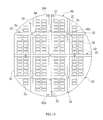
- the lid substrate forming wafer 50 is formed into a circular shape as viewed in a plan view and, at the same time, a reference mark portion A 1 is formed on an outer peripheral portion of the wafer 50 by cutting away the outer peripheral portion along a straight line (chord) which connects two points on an outer periphery of the wafer 50 .
- a recessed portion forming step where a large number of recessed portions 3 a for cavities C are formed on a bonding surface of the lid substrate forming wafer 50 is performed (S 22 ) and, at the same time, a groove forming step where grooves 22 are formed (S 23 ) and a through hole forming step where the through holes 21 are formed (S 24 ) are performed.
- the recessed portions 3 a are formed on a portion 50 c of the bonding surface of the lid substrate forming wafer 50 which is positioned more inside in the radial direction than an outer peripheral portion 50 b (hereinafter, the portion 50 c being referred to as a product region).
- the plurality of recessed portions 3 a are formed on the product region 50 c at intervals in one direction, and are also formed at intervals in the other direction perpendicular to one direction.
- the recessed portions 3 a are formed over the substantially whole region of the bonding surface of the lid substrate forming wafer 50 except for the outer peripheral portion 50 b.
- the grooves 22 are formed in a grid shape on the bonding surface of the lid substrate forming wafer 50 , for example, and are opened outwardly in the radial direction at a radial end portion (outer periphery) of the lid substrate forming wafer 50 .
- the grooves 22 are formed such that two grooves 22 are radially formed on the bonding surface of the lid substrate forming wafer 50 equidistantly about the center of the wafer 50 , and a plurality of grooves 22 are formed parallel to these two grooves 22 at predetermined intervals.
- a width of the groove 22 is set smaller than a longitudinal length of the recessed portion 3 a which is formed into a rectangular shape as viewed in a plan view.
- the plurality of through holes 21 are formed in the grooves 22 in a state where the through holes 21 penetrate the lid substrate forming wafer 50 in the thickness direction (in the laminating direction described later).
- the through hole 21 is formed at a position of a lattice point arranged in the grid-like grooves 22 at the center of the wafer 50 , at positions of lattice points arranged in the grid-shaped grooves 22 on the circumference C 1 having a predetermined first radius, and at positions arranged in the grooves 22 on the circumference C 2 having a radius smaller than the radius of the circumference C 1 .
- the recessed portions 3 a, the grooves 22 and the through holes 21 may be formed simultaneously by etching the lid substrate forming wafer 50 .
- the recessed portions 3 a, the grooves 22 and the through holes 21 may be simultaneously formed by pressing the lid substrate forming wafer 50 from above and below while heating the lid substrate forming wafer 50 by making use of jigs.
- the recessed portions 3 a, the grooves 22 , and the through holes 21 may be also formed simultaneously by applying a glass paste to desired portions on the lid substrate forming wafer 50 by screen printing.
- the first wafer preparation step is finished at this point of time.
- a second wafer preparation step is performed (S 30 ).
- a base substrate forming wafer 40 which becomes the base substrate 2 later is prepared up to a state immediately before the base substrate 2 is bonded to the lid substrate 3 by anodic bonding.
- soda-lime glass is polished to a predetermined thickness and is cleaned and, thereafter, a layer degenerated by working which forms an outermost surface is removed by etching or the like thus forming a disc-shaped base substrate forming wafer 40 (S 31 ).
- the base substrate forming wafer 40 is, as shown in FIG. 13 , formed into a circular shape as viewed in a plan view and, at the same time, a reference mark portion A 2 is formed on an outer peripheral portion of the wafer 40 by cutting away the outer peripheral portion along a straight line (chord) which connects two points on an outer periphery of the wafer 40 .
- positioning holes 40 d in which a positioning pin of an anodic bonding device 30 described later is inserted are formed.
- a through hole forming step is performed (S 32 ). In this step, plural pairs of through holes 25 which penetrate the base substrate forming wafer 40 are formed.
- a dotted line M shown in FIG. 11 indicates a cutting line along which the wafer bonded body 60 is cut in a cutting step performed later.
- the through holes 25 are formed by a method such as a sandblast method, a press forming method using a jig or the like, for example.
- the pair of through holes 25 is formed in the base substrate forming wafer 40 at positions where the pair of through holes 25 is arranged within each recessed portion 3 a formed on the lid substrate forming wafer 50 when both wafers 40 , 50 are made to overlap each other later, and also one through hole 25 is arranged on a base portion 12 side of the piezoelectric vibrating piece 4 which is mounted on the wafer 40 later and the other through hole 25 is arranged on a distal end side of the vibrating arm portion 11 .
- the pair of through holes 25 is, on the bonding surface of the base substrate forming wafer 40 , formed in a portion 40 c (hereinafter, referred to as a product region) which is positioned more inside in the radial direction than the outer peripheral portion 40 b.
- the plural pairs of through holes 25 are formed in the product region 40 c at intervals in one direction and are also formed at intervals in the other direction perpendicular to one direction.
- the plural pairs of through holes 25 are formed in the substantially whole region of the bonding surface of the base substrate forming wafer 40 except for the outer peripheral portion 40 b.
- a through electrode forming step is performed (S 33 ).
- the pair of through electrodes 26 is formed by filling the pair of through holes 25 with a conductive body not shown in the drawing.
- a bonding film forming step (S 34 ) is performed.
- the bonding film 27 is formed on the bonding surface of the base substrate forming wafer 40 by patterning using a conductive material.
- a routing electrode forming step is performed (S 35 ). In this step, the plurality of routing electrodes 28 which are respectively electrically connected to the pair of through electrodes 26 are formed.
- one through electrode 26 and one routing electrode 28 are made conductive with each other and, at the same time, the other through electrode 26 and the other routing electrode 28 are made conductive with each other.
- the second wafer preparation step is finished at this point of time.
- a dotted line M shown in FIG. 12 and FIG. 13 indicates a cutting line along which the wafer bonded body 60 is cut in a cutting step performed later. Further, in FIG. 13 , the bonding film 27 is omitted.
- the order of steps is set such that the routing electrode forming step (S 35 ) is performed after the bonding film forming step (S 34 ).
- the bonding film forming step (S 34 ) may be performed after the routing electrode forming step (S 35 ) or both steps may be simultaneously performed.
- a mounting step is performed (S 40 ).
- a plurality of prepared piezoelectric vibrating pieces 4 are respectively bonded to a surface of the base substrate forming wafer 40 by bump bonding via the routing electrodes 28 .
- the bump B made of gold or the like is formed on the pair of routing electrodes 28 respectively. Then, the base portions 12 of the piezoelectric vibrating pieces 4 are mounted on the bumps B and, thereafter, the piezoelectric vibrating pieces 4 are pressed to the bumps B while heating the bumps B at a predetermined temperature.
- the piezoelectric vibrating pieces 4 are mechanically supported on the bumps B and, at the same time, the mount electrodes 14 and the routing electrodes 28 are electrically connected to each other.
- the pair of excitation electrodes 13 of the piezoelectric vibrating piece 4 is respectively made conductive with the pair of through electrodes 26 .
- the piezoelectric vibrating piece 4 is bonded by bump bonding and hence, the piezoelectric vibrating piece 4 is supported in a floating state from the bonding surface of the base substrate forming wafer 40 .
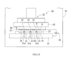
- the base substrate forming wafer 40 and the lid substrate forming wafer 50 are set in the anodic bonding device 30 .
- the anodic bonding device 30 includes a lower jig 31 made of a conductive material, an upper jig 33 which is supported by a pressurizing means 32 in a state where the upper jig 33 can be advanced or retracted with respect to the lower jig 31 , and an energizing means 34 which electrically connects the bonding film 27 formed on the base substrate forming wafer 40 which is set on the upper jig 33 and the lower jig 31 to each other.
- the anodic bonding device 30 is arranged in a vacuum chamber 61 .
- the lid substrate forming wafer 50 is set on the lower jig 31 in a state where the recessed portions 3 a are opened toward the upper jig 33 , and the base substrate forming wafer 40 is set on the upper jig 33 in a state where the piezoelectric vibrating pieces 4 are made to face the recessed portions 3 a formed on the lid substrate forming wafer 50 in an opposed manner
- positioning pins not shown in the drawings which are formed on the anodic bonding device 30 are inserted into the positioning holes 40 d, 50 d formed in the respective wafers 40 , 50 so that the respective wafers 40 , 50 are aligned with each other in the surface direction of the respective wafers 40 , 50 .
- the lower jig 31 on which the lid substrate forming wafer 50 is set includes communication holes 31 a by which the through holes 21 formed in the lid substrate forming wafer 50 and the inside of the vacuum chamber 61 communicate with each other and hence, the through holes 21 and the communication holes 31 a communicate with each other in a state where the respective wafers 40 , 50 are aligned with each other.
- an overlapping step is performed (S 50 ).
- the upper jig 33 is forwardly moved toward the lower jig 31 by driving the pressurizing means 32 so that the piezoelectric vibrating pieces 4 mounted on the base substrate forming wafer 40 enter the inside of the recessed portions 3 a of the lid substrate forming wafer 50 , the base substrate forming wafer 40 and the lid substrate forming wafer 50 are laminated in a state where the respective wafers are sandwiched between the upper jig 33 and the lower jig 31 from both sides in the laminating direction (that is, the moving direction of the upper jig 33 ) whereby these wafers 40 , 50 are made to overlap each other.
- the piezoelectric vibrating pieces 4 mounted on the base substrate forming wafer 40 are respectively housed in the cavities C formed between both wafers 40 , 50 .
- a bonding step is performed (S 60 ).
- the base substrate forming wafer 40 and the lid substrate forming wafer 50 are bonded to each other by anodic bonding by applying a predetermined voltage under a predetermined temperature.
- a predetermined voltage is applied between the bonding film 27 of the base substrate forming wafer 40 and the lower jig 31 by the energizing means 34 .
- the piezoelectric vibrating pieces 4 can be sealed in the cavities C and hence, it is possible to obtain a wafer bonded body 60 shown in FIG. 15 where the base substrate forming wafer 40 and the lid substrate forming wafer 50 are bonded to each other.
- FIG. 15 to facilitate the understanding of the drawing, the wafer bonded body 60 is shown in an exploded manner, and the bonding film 27 is omitted from the base substrate forming wafer 40 in the drawing.
- a dotted line M shown in FIG. 15 indicates a cutting line along which the wafer bonded body 60 is cut in a cutting step performed later.
- the through holes 25 which are formed in the base substrate forming wafer 40 are completely closed by the through electrodes 26 and hence, there exists no possibility that the air-tightness in the cavity C is deteriorated through the through holes 25 .
- the gas can be discharged into the inside of the vacuum chamber 61 from between the base substrate forming wafer 40 and the lid substrate forming wafer 50 through the through holes 21 formed in the grooves 22 and the communication holes 31 a which communicate with the through holes 21 and the inside of the vacuum chamber 61 thus ensuring the desired degree of vacuum in the cavities C.
- a gas for example, an oxygen gas or the like
- an external electrode forming step is performed (S 70 ).
- a plural pairs of external electrodes 29 each of which is respectively electrically connected to each pair of through electrodes 26 are formed by patterning using a conductive material.
- a fine adjustment step is performed (S 90 ).
- frequency of the individual piezoelectric vibrating piece 4 sealed in the cavity C is finely adjusted in the form of the wafer bonded body 60 such that the frequency falls within a predetermined range.
- a voltage is applied to the external electrodes 29 thus vibrating the piezoelectric vibrating piece 4 .
- a laser beam is irradiated from the outside through the lid substrate forming wafer 50 while measuring frequency thus evaporating the fine adjustment 17 b of the weight metal film 17 .
- a weight of a distal end side of the pair of vibrating arm portions 10 , 11 is changed and hence, it is possible to perform the fine adjustment such that the frequency of the piezoelectric vibrating piece 4 falls within a predetermined range of nominal frequency.
- a cutting step is performed (S 100 ).
- the wafer bonded body 60 formed by bonding the base substrate forming wafer 40 and the lid substrate forming wafer 50 is cut into small pieces along the cutting lines M shown in FIG. 15 .
- the fine adjustment step (S 90 ) is performed after cutting the wafer bonded body 60 into individual piezoelectric vibrators 1 by performing the cutting step (S 100 ).
- the fine adjustment step (S 90 ) prior to the cutting step (S 100 ) can be performed in the form of the wafer bonded body 60 and hence, it is possible to perform the fine adjustment of the plurality of piezoelectric vibrators 1 more efficiently.
- resonance frequency, a resonance resistance value, a drive level characteristic (dependency of resonance frequency and resonance resistance value on excitation power) and the like of the piezoelectric vibrating piece 4 are checked by measuring.
- the manufacture of the piezoelectric vibrator 1 is finished with this step.
- the through holes 21 are formed in the lid substrate forming wafer 50 and hence, an oxygen gas generated between both wafers 40 , 50 in performing the previously-mentioned bonding step can be easily discharged to the outside from between both wafers 40 , 50 through the through holes 21 and the communication holes 31 a whereby it is possible to suppress the manufacture of the piezoelectric vibrators 1 which exhibit the low degree of vacuum in the cavity C.
- the through holes 21 are formed in the lid substrate forming wafer 50 which includes the recessed portions 3 a. Accordingly, the through holes 21 can be simultaneously formed with the formation of the recessed portions 3 a by press forming, etching or the like and hence, the wafer 50 can be formed efficiently.
- the through hole 21 is formed at the center of the lid substrate forming wafer 50 and hence, the through hole 21 can be more surely deformed by strain generated in the lid substrate forming wafer 50 in the course of the bonding step whereby the product regions 40 c, 50 c of both wafers 40 , 50 can be more surely bonded to each other over the approximately whole region.
- the through hole 21 is formed at the center where an oxygen gas generated between these wafers 40 , 50 at the time of bonding both wafers 40 , 50 is liable to stay and hence, the piezoelectric vibrators 1 are not manufactured from such center whereby it is possible to surely suppress the manufacture of the piezoelectric vibrators 1 which exhibit the low degree of vacuum in the cavity C.
- the through holes 21 are formed in the lid substrate forming wafer 50 in the above-mentioned embodiment, the through holes 21 may be formed in the base substrate forming wafer 40 .
- the communication holes which make the through holes formed in the base substrate forming wafer 40 and the inside of the vacuum chamber 61 communicate with each other may be formed in the upper jig 33 .
- the shape of the through holes 21 is not limited to such a shape, and may be a polygonal shape, a slit shape which extends in the radial direction or the like.
- the lid substrate forming wafer 50 includes the grooves 22 which extend in the radial direction and the through holes 21 are formed in the grooves 22 and hence, an oxygen gas generated between both wafers 40 , 50 at the time of bonding can be surely discharged to the outside from between these wafers 40 , 50 .
- the grooves 22 open outwardly in the radial direction at the radial end portion of the lid substrate forming wafer 50 and hence, an oxygen gas generated between both wafers 40 , 50 at the time of bonding can be easily discharged into the vacuum chamber 61 .
- the radial outer ends of the grooves 22 are positioned more inwardly in the radial direction than outer peripheries of the wafers 40 , 50 .
- the bonding film 27 is not formed on the portion which is positioned more outwardly in the radial direction than the radial outer end of the groove 22 .
- the product region where the recessed portion 3 a can be formed in the lid substrate forming wafer 50 can be easily ensured widely and hence, the number of package products which can be formed at a time can be increased. That is, a yield ratio can be enhanced.
- the piezoelectric vibrating piece 4 is bonded by bump bonding.
- the bonding of the piezoelectric vibrating piece 4 is not limited to the bump bonding.
- the piezoelectric vibrating piece 4 may be bonded using a conductive adhesive agent.
- the piezoelectric vibrating piece 4 can be floated from the base substrate 2 and hence, a minimum vibration gap necessary for vibrations can be naturally ensured.
- the piezoelectric vibrator 1 is exemplified as a package product.
- the package product is not limited to the piezoelectric vibrator 1 , and may be suitably changed without being limited to the piezoelectric vibrator 1 .
- the through hole 21 and the communication hole 31 a may have the same shape or the different shapes.
- the through holes 21 may be formed in portions other than the grooves 22 .
- the oscillator 100 of this embodiment is, as shown in FIG. 16 , formed as an oscillating element in which the piezoelectric vibrator 1 is electrically connected to an integrated circuit 101 .
- the oscillator 100 includes a substrate 103 on which an electronic part 102 such as a capacitor is mounted.
- the above-mentioned integrated circuit 101 for oscillator is mounted on the substrate 103 , and the piezoelectric vibrating element 4 of the piezoelectric vibrator 1 is mounted on the substrate 103 in the vicinity of the integrated circuit 101 .
- the electronic part 102 , the integrated circuit 101 and the piezoelectric vibrator 1 are electrically connected with each other by a wiring pattern not shown in the drawing.
- the respective constitutional parts are molded by a resin not shown in the drawing.
- the piezoelectric vibrating piece 4 arranged in the piezoelectric vibrator 1 vibrates.
- This vibration is converted into an electric signal due to a piezoelectric characteristic which the piezoelectric vibrating piece 4 possesses, and the electric signal is inputted to the integrated circuit 101 .
- the piezoelectric vibrator 1 functions as an oscillating element.
- an RTC (real time clock) module or the like corresponding to a request, it is possible to impart, besides a function as a timepiece-use single-function oscillator or the like, a function of controlling an operation date and time of the oscillator or an external device or a function of providing time, calendar and the like to the oscillator 100 .
- the oscillator 100 includes the high-quality piezoelectric vibrator 1 with the high operational reliability and hence, the oscillator 100 per se can acquire the high quality in the same manner as the piezoelectric vibrator 1 .
- the electronic apparatus is explained in conjunction with FIG. 17 .
- the explanation is made with respect to an example where the electronic apparatus is a portable information device 110 which includes the above-mentioned piezoelectric vibrator 1 .
- the portable information device 110 of this embodiment is a device which is represented by a mobile phone, for example, and is a developed or improved form of a wrist watch of the related art.
- the portable information device 110 resembles the wrist watch in appearance.
- a liquid crystal display is arranged on a portion of the portable information device 110 which corresponds to a dial of the wrist watch, and a present time or the like can be displayed on a screen of the liquid crystal display.
- the portable information device 110 when used as a communication device, a user removes the portable information device 110 from his wrist, and performs communication in the same manner as a mobile phone of the related art by a speaker and a microphone incorporated into an inner portion of a band.
- the portable information device 110 is remarkably miniaturized and light-weighted compared to the conventional mobile phone.
- the portable information device 110 includes, as shown in FIG. 17 , a piezoelectric vibrator 1 and a power source part 111 for power supply.
- the power source part 111 is formed of a lithium secondary battery, for example.
- a control part 112 which performs various controls, a timer part 113 which counts time or the like, a communication part 114 which performs communication with the outside, a display part 115 which displays various information, and a voltage detection part 116 which detects voltages of the respective functional parts are connected to each other in parallel.
- Electricity is supplied to the respective functional parts from the power source part 111 .
- the control part 112 performs the transmission and the reception of voice data, the measurement, display and the like of a present time and an operational control of the whole system by controlling the respective functional parts. Further, the control part 112 includes a ROM in which programs are preliminarily written, a CPU which reads and executes the programs written in the ROM, a RAM which is used as a work area of the CPU and the like.
- the timer part 113 includes an integrated circuit which incorporates an oscillation circuit, a register circuit, a counter circuit, an interface circuit and the like therein, and the piezoelectric vibrator 1 .
- the piezoelectric vibrating piece 4 vibrates, the vibrations are converted into an electric signal due to a piezoelectric characteristic which crystal possesses, and the electric signal is inputted to the oscillation circuit.
- An output of the oscillation circuit is binalized and the binalized value is counted by the register circuit and the counter circuit.
- the transmission/reception of signals is performed between the timer part 113 and the control part 112 via the interface circuit, and a present time, a present date, calendar information and the like are displayed on the display part 115 .
- the communication part 114 has the substantially same functions as a conventional mobile phone, and includes a wireless part 117 , a voice processing part 118 , a switching part 119 , an amplifying part 120 , a voice inputting/outputting part 121 , a telephone number inputting part 122 , an incoming call sound generation part 123 , and a calling-control memory part 124 .
- the wireless part 117 performs the transmission/reception of various data such as voice data with a base station through an antenna 125 .
- the voice processing part 118 performs coding and decoding of a voice signal inputted from the wireless part 117 or the amplifying part 120 .
- the amplifying part 120 amplifies a signal received from the voice processing part 118 or the voice inputting/outputting part 121 to a predetermined level.
- the voice inputting/outputting part 121 is formed of a speaker, a microphone or the like, and makes an incoming call sound or a received voice loud or collects voice.
- the incoming call sound generation part 123 generates an incoming call sound in response to calling from a base station.
- the switching part 119 switches the amplifying part 120 connected to the voice processing part 118 to the incoming call sound generation part 123 when a call arrives so that an incoming call sound generated by the incoming call sound generation part 123 is outputted to the voice inputting/outputting part 121 through the amplifying part 120 .
- the calling control memory part 124 stores a program relating to an incoming/outgoing call control in communication.
- the telephone number inputting part 122 includes, for example, numeral keys ranging from 0 to 9 and other keys. By pushing these numeral keys or the like, a user can input the telephone number of call destination or the like.
- the voltage detection part 116 when a voltage applied to the respective functional parts such as the control part 112 from the power source part 111 becomes lower than a predetermined value, detects such lowering of voltage and notifies the lowering of voltage to the control part 112 .
- the predetermined voltage value at this point of time is a value which is preliminarily set as minimum voltage necessary for stably driving the communication part 114 , and is set to approximately 3V, for example.
- the control part 112 which receives the notification of the lowering of voltage from the voltage detection part 116 prohibits operations of the wireless part 117 , the voice processing part 118 , the switching part 119 and the incoming call sound generation part 123 .
- the operation stop of the wireless part 117 which consumes large power is inevitable. Further, a message that a remaining battery quantity is short so that the communication part 114 is inoperable is displayed on the display part 115 .
- an operation of the communication part 114 can be prohibited and a message which indicates the prohibition of the operation of the communication part 114 can be displayed on the display part 115 .
- This display may be formed of a character message.
- a ⁇ (bad) mark may be attached to a telephone icon displayed on an upper part of a display screen of the display part 115 .
- the electronic apparatus is provided with a power source breaking part 126 which can selectively break a power source of a portion relating to a function of the communication part 114 . In this case, it is possible to stop the function of the communication part 114 more reliably.
- the portable information device 110 includes the high-quality piezoelectric vibrator 1 with the high operational reliability and hence, the portable information device 110 per se can acquire the high quality in the same manner as the piezoelectric vibrator 1 .
- the radio-controlled timepiece 130 of this embodiment is, as shown in FIG. 18 , a timepiece which includes the piezoelectric vibrator 1 which is electrically connected to a filter part 131 , and has a function of receiving a standard electric wave containing timepiece information, automatically correcting time to correct time, and displaying the corrected time.
- transmission installations which transmit the standard electric wave are located in Fukushima prefecture (40 kHz) and Saga prefecture (60 kHz) and transmit the standard electric waves respectively.
- a long wave having frequency of 40 kHz or 60 kHz has both of property that the wave propagates on a ground and property that the wave propagates while being reflected between an ionosphere and a ground and hence, the long wave has a wide propagation range whereby the standard electric wave can cover all areas of Japan with the above-mentioned two transmission installations.
- the functional constitution of the radio-controlled timepiece 130 is explained in detail hereinafter.
- the antenna 132 receives the standard electric wave formed of a long wave having frequency of 40 kHz or 60 kHz.
- the standard electric wave formed of a long wave is an electric wave which is obtained by AM-modulating a carrier wave having frequency of 40 kHz or 60 kHz by time information called as a time code.
- the received standard electric wave formed of a long wave is amplified by an amplifier 133 , and is filtered by a filter part 131 having a plurality of piezoelectric vibrators 1 , and is tuned.
- the piezoelectric vibrators 1 of this embodiment include crystal vibrator parts 138 , 139 having resonance frequency of 40 kHz or 60 kHz as same as the above-mentioned frequency of the carrier wave respectively.
- a filtered signal of predetermined frequency is detected and demodulated by a detection/rectifying circuit 134 .
- the time code is taken out through a waveform shaping circuit 135 , and is counted by a CPU 136 .
- the CPU 136 reads information on present year, cumulative days, day of week, time and the like. The read information is reflected on an RTC 137 so that correct time information is displayed.
- the carrier wave has frequency of 40 kHz or 60 kHz and hence, the crystal vibrator parts 138 , 139 are preferably formed of a vibrator having the above-mentioned tuning-fork structure.
- the frequencies of standard electric waves of long wave used overseas differ from the standard electric wave used in Japan.
- the standard electric wave having frequency of 77.5 kHz is used in Germany. Accordingly, in incorporating the radio-controlled timepiece 130 also compatible with the oversea use into a portable device, the piezoelectric vibrator 1 having frequency different from the frequency used in Japan becomes necessary.
- the radio-controlled timepiece 130 includes the high-quality piezoelectric vibrator 1 with high operational reliability and hence, the radio-controlled timepiece 130 per se can acquire the high quality in the same manner as the piezoelectric vibrator 1
- the explanation has been made by taking the piezoelectric vibrator 1 where the piezoelectric vibrating piece 4 is sealed in the package 9 as an electronic part as an example.
- the present invention is not limited to the piezoelectric vibrator 1 and is applicable to a device other than the piezoelectric vibrator which seals an electronic part other than the piezoelectric vibrating piece 4 therein.
- the piezoelectric vibrating piece 4 is not limited to a tuning-fork-type piezoelectric vibrating piece, and may be a thickness-shear piece-type vibrating piece formed by AT cutting.
- the tuning-fork-type piezoelectric vibrating piece 4 in the above-mentioned embodiment, the explanation has been made by taking the groove-type piezoelectric vibrating piece 4 where the groove portions 18 are formed on both main surfaces of the vibrating arm portions 10 , 11 as an example. However, it is also possible to adopt a type of piezoelectric vibrating piece having no grooves.
Abstract
Description
- This application claims priority under 35 U.S.C. §119 to Japanese Patent Application No. 2011-070536 filed on Mar. 28, 2011, the entire content of which is hereby incorporated by reference.
- 1. Field of the Invention
- The present invention relates to a manufacturing method of a package which can seal an electronic part in a cavity.
- 2. Description of the Related Art
- Recently, a package product having the following constitution has been popularly used. The package product includes a base substrate and a lid substrate which are bonded to each other by anodic bonding in a laminated state so as to form a cavity therebetween, and an operating piece which is mounted on a portion of the base substrate positioned inside the cavity.
- As this type of package product, for example, there has been known a piezoelectric vibrator which is mounted on a mobile phone or a personal digital assist and makes use of crystal or the like as a time source, a timing source for a control signal or the like, a reference signal source or the like.
- Also, there has been known a method where such a package product is formed as follows (see JP-A-2006-339896).
- Firstly, a base substrate forming wafer and a lid substrate forming wafer are set in an anodic bonding device arranged in a vacuum chamber, and these base substrate forming wafer and lid substrate forming wafer are overlapped to each other by way of a bonding film for anodic bonding which is made of a conductive material.
- On a bonding surface of the lid substrate forming wafer, a plurality of recessed portions which form cavities when the lid substrate forming wafer overlaps the base substrate forming wafer are formed.
- On a bonding surface of the base substrate forming wafer, a plurality of operating pieces are mounted corresponding to the plurality of recessed portions formed on the lid substrate forming wafer, and a bonding film is formed on a portion of the bonding surface except for portions where the operating pieces are mounted.
- Then, the lid substrate forming wafer is set on an electrode plate of the anodic bonding device.
- Next, while activating ions in the lid substrate forming wafer by heating the lid substrate forming wafer, a voltage is applied between the bonding film of the base substrate forming wafer and the electrode plate thus supplying an electric current to the lid substrate forming wafer.
- Accordingly, an electrochemical reaction is generated on an interface between the bonding film and a bonding surface of the lid substrate forming wafer so that the bonding film of the base substrate forming wafer and the lid substrate forming wafer are bonded to each other by anodic bonding thus forming a wafer bonded body.
- Thereafter, a plurality of package products are formed by cutting the wafer bonded body at predetermined positions.
- However, the above-mentioned method relating to the prior art has a tendency that, at the time of anodic bonding, with respect to the base substrate forming wafer and the lid substrate forming wafer (both wafers), outer peripheral portions of these wafers are bonded earlier than center portions of these wafers in a cavity or in a product region where operating pieces are arranged.
- Along with such a tendency, for example, there may be a case where strain or warping occurs at the center portions so that a gas which is generated between both wafers at the time of bonding is liable to stay between the center portions.
- In such a case, the degree of vacuum in the cavity of the acquired package product is lowered through the center portions and hence, there is a possibility that a package product which does not have the desired performance is produced.
- The present invention has been made in view of the above-mentioned circumstances, and it is an object of the present invention to provide a manufacturing method of a package, a piezoelectric vibrator, an oscillator, an electronic apparatus and a radio-controlled timepiece where a gas generated between two wafers (a base substrate forming wafer and a lid substrate forming wafer) at the time of bonding these wafers to each other can be easily discharged to the outside.
- To achieve the above-mentioned object by overcoming the above-mentioned object, according to one aspect of the present invention, there is provided a manufacturing method of a package including the steps of: forming a plurality of cavities each of which seals an electronic part (a piezoelectric vibrating
piece 4 in an embodiment described later, for example) between a base substrate (a basesubstrate forming wafer 40 in the embodiment described later, for example) and a lid substrate (a lidsubstrate forming wafer 50 in the embodiment described later, for example) by laminating the base substrate and the lid substrate to each other by sandwiching from both sides in the laminating direction using a jig (alower jig 31 andupper jig 33 in the embodiment described later, for example) arranged inside a vacuum chamber (avacuum chamber 61 in the embodiment described later, for example); forming a bonded body (a wafer bondedbody 60 in the embodiment described later, for example) by bonding the base substrate and the lid substrate to each other by anodic bonding in a state where the base substrate and the lid substrate are pressurized in the laminating direction; and forming a plurality of packages by cutting the bonded body for every one of plurality of cavities, wherein at least the base substrate or the lid substrate has a through hole (throughhole 21 in the embodiment described later, for example) which penetrates the base substrate or the lid substrate in the laminating direction, a communication hole (communication hole 31 a in the embodiment described later, for example) which makes the through hole and the inside of the vacuum chamber communicate with each other is formed in the jig, and the base substrate and the lid substrate are laminated to each other in a state where the through hole and the communication hole are made to communicate with each other at the time of forming the bonded body by the anodic bonding. - According to the manufacturing method of the present invention, the communication holes which make the through hole which is formed at least in the base substrate or in the lid substrate and the vacuum chamber communicate with each other are formed in the jig which laminates the base substrate and the lid substrate by sandwiching from both sides in the laminating direction.
- Accordingly, a gas generated between the base substrate and the lid substrate at the time of bonding the base substrate and the lid substrate can be easily discharged to the inside of the vacuum chamber from between the base substrate and the lid substrate through the through hole and the communication hole whereby a plurality of packages which ensure the desired degree of vacuum in the cavity can be easily manufactured.
-
FIG. 1 is a perspective view showing the appearance of a piezoelectric vibrator according to an embodiment of the present invention; -
FIG. 2 is a view showing the internal constitution of the piezoelectric vibrator shown inFIG. 1 , and is also a view showing a piezoelectric vibrating piece as viewed from above in a state where a lid substrate is removed; -
FIG. 3 is a cross-sectional view of the piezoelectric vibrator taken along a line A-A inFIG. 2 ; -
FIG. 4 is a cross-sectional view of the piezoelectric vibrator taken along a line B-B inFIG. 2 ; -
FIG. 5 is an exploded perspective view of the piezoelectric vibrator shown inFIG. 1 ; -
FIG. 6 is a top plan view of the piezoelectric vibrating piece which constitutes the piezoelectric vibrator shown inFIG. 1 ; -
FIG. 7 is a bottom plan view of the piezoelectric vibrating piece shown inFIG. 5 ; -
FIG. 8 is a cross-sectional view as viewed in the direction indicated by an arrow C-C inFIG. 6 ; -
FIG. 9 is a flowchart showing the flow of manufacturing steps of the piezoelectric vibrator shown inFIG. 1 ; -
FIG. 10 is a view showing one step in manufacturing the piezoelectric vibrator along the flowchart shown inFIG. 9 and is also a view showing one embodiment where recessed portions are formed on a lid substrate forming wafer from which a lid substrate is produced; -
FIG. 11 is a view showing one step in manufacturing the piezoelectric vibrator along the flowchart shown inFIG. 9 , and is also a view showing a state where one pair of through holes is formed in a base substrate forming wafer from which a base substrate is produced; -
FIG. 12 is a view showing a state where through electrodes are formed in the pair of through hole and a bonding film and a routing electrode are formed by patterning on an upper surface of the base substrate forming wafer after a state shown inFIG. 11 ; -
FIG. 13 is a view showing the whole base substrate forming wafer in a state shown inFIG. 12 ; -
FIG. 14 is a schematic view showing a state where the base substrate forming wafer and the lid substrate forming wafer according to the embodiment of the present invention are set on an anodic bonding device; -
FIG. 15 is a view showing one step in manufacturing the piezoelectric vibrator along the flowchart shown inFIG. 9 , and is also an exploded perspective view of a wafer bonded body which is formed by bonding the base substrate forming wafer and the lid substrate forming wafer by anodic bonding in a state where the piezoelectric vibrating piece is housed in a cavity; -
FIG. 16 is a constitutional view showing one embodiment of an oscillator according to the present invention; -
FIG. 17 is a constitutional view showing one embodiment of an electronic apparatus according to the present invention; and -
FIG. 18 is a constitutional view showing one embodiment of a radio-controlled timepiece according to the present invention. - Hereinafter, the explanation is made with respect to a manufacturing method of a package, a piezoelectric vibrator which includes a package manufactured by the manufacturing method of a package, and an oscillator, an electronic apparatus and a radio-controlled timepiece which respectively include the piezoelectric vibrator according to one embodiment of the present invention.
- In this embodiment, the explanation is made by taking a piezoelectric vibrator as a package which includes a base substrate and a lid substrate which are bonded to each other by anodic bonding in a laminated state so as to form a cavity therebetween, and an operating piece which is mounted on a portion of the base substrate positioned inside the cavity as an example.
- The
piezoelectric vibrator 1 is, as shown inFIG. 1 toFIG. 5 , for example, a surface-package-type piezoelectric vibrator where thepiezoelectric vibrator 1 is formed into a box shape by laminating thebase substrate 2 and thelid substrate 3 in two layers, and a piezoelectric vibrating piece (operating piece) 4 is housed in a cavity C formed in thepiezoelectric vibrator 1. - In
FIG. 5 , to facilitate the understanding of drawings,excitation electrodes 13,lead electrodes 16,mount electrodes 14 andweight metal films 17 described later are omitted from the drawings. - As shown in
FIG. 6 toFIG. 8 , thepiezoelectric vibrating piece 4 is a tuning-fork-type vibrating piece which is made of a piezoelectric material such as crystal, lithium tantalate or lithium niobate, and the piezoelectric vibratingpiece 4 is vibrated when a predetermined voltage is applied to thepiezoelectric vibrating piece 4. - The piezoelectric vibrating
piece 4 includes a pair of vibratingarm portions base portion 12 to which proximal end sides of the pair of vibratingarm portions excitation electrodes 13 which are formed on outer surfaces of the pair of vibratingarm portions arm portions mount electrodes 14 which are electrically connected to theexcitation electrodes 13. - Further, the piezoelectric vibrating
piece 4 of this embodiment includesgroove portions 15 which are formed on both main surfaces of the pair of vibratingarm portions arm portions groove portion 15 extends from a proximal end side to an area in the vicinity of an intermediate portion of the vibratingarm portions - The
excitation electrodes 13 are electrodes for vibrating the pair of vibratingarm portions arm portions arm portions excitation electrodes 13 are electrically separated from each other. - To be more specific, as shown in
FIG. 8 , oneexcitation electrode 13 is mainly formed on thegroove portions 15 of one vibratingarm portion 10 and on both side surfaces of the other vibratingarm portion 11, while theother excitation electrode 13 is mainly formed on both side surfaces of one vibratingarm portion 10 and on thegroove portions 15 of the other vibratingarm portion 11. - Further, as shown in
FIG. 6 andFIG. 7 , theexcitation electrodes 13 are electrically connected to themount electrodes 14 through thelead electrodes 16 respectively on both main surfaces of thebase portion 12. A voltage is applied to the piezoelectric vibratingpiece 4 through themount electrodes 14. Here, the above-mentionedexcitation electrodes 13, themount electrodes 14 and thelead electrodes 16 are respectively films formed of a conductive film made of chromium (Cr), nickel (Ni), aluminum (Al), titanium (Ti) or the like by coating, for example. - A
weight metal film 17 is formed on distal ends of the pair of vibratingarm portions weight metal film 17 is provided for performing the adjustment (frequency adjustment) such that the pair of vibratingaim portions - Here, the
weight metal film 17 is constituted of acoarse adjustment film 17 a which is used for coarsely adjusting the frequency and afine adjustment film 17 b which is used for finely adjusting the frequency. - By performing the frequency adjustment using these
coarse adjustment films 17 a and thefine adjustment films 17 b, it is possible to make the frequency of the pair of vibratingarm portions - As shown in
FIG. 2 ,FIG. 3 andFIG. 5 , the piezoelectricvibrating piece 4 having such a constitution is bonded to an upper surface of thebase substrate 2 by bump bonding using a bump B made of gold or the like. - To be more specific, the piezoelectric vibrating
piece 4 is bonded to thebase substrate 2 in a state where a pair ofmount electrodes 14 is bonded to two bumps B which are formed onrouting electrodes 28 described later by bump bonding in a contact state. - Due to such a constitution, the piezoelectric vibrating
piece 4 is supported in a state where the piezoelectric vibratingpiece 4 floats from the upper surface of thebase substrate 2 and, at the same time, themount electrodes 14 and therouting electrodes 28 are respectively electrically connected to each other. - The above-mentioned
lid substrate 3 is a transparent insulation substrate made of a glass material such as soda-lime glass, for example, and has a plate shape as shown inFIG. 1 ,FIG. 3 ,FIG. 4 andFIG. 5 . - A recessed
portion 3 a having a rectangular shape as viewed in a plan view in which the piezoelectric vibratingpiece 4 is housed is formed on a bonding surface of thelid substrate 3 to which thebase substrate 2 is bonded. - The recessed
portion 3 a forms the cavity C in which the piezoelectric vibratingpiece 4 is housed when bothsubstrates - Further, the recessed
portion 3 a is closed by thebase substrate 2 due to the anodic bonding of thelid substrate 3 and thebase substrate 2. - The
base substrate 2 is, in the same manner as thelid substrate 3, a transparent insulation substrate made of a glass material such as soda-lime glass, for example, and as shown inFIG. 1 toFIG. 5 , has a plate shape with a size which allows thebase substrate 2 to overlap thelid substrate 3. - A pair of through
holes 25 which penetrates thebase substrate 2 is formed in thebase substrate 2. - The pair of through
holes 25 is formed such that the pair of throughholes 25 is arranged within the cavity C. - To explain the structure in more detail, the through
holes 25 are formed such that one throughhole 25 is positioned on abase portion 12 side of the mounted piezoelectric vibratingpiece 4, and the other throughhole 25 is positioned on a distal end side of the vibratingarm portions - In the example shown in the drawing, the explanation is made by taking the through
hole 25 which has the substantially same inner diameter over the whole region in the plate thickness direction of thebase substrate 2 as an example. However, the present invention is not limited to such a constitution and, for example, the through hole may be formed into a tapered shape whose inner diameter is gradually narrowed or expanded along the plate thickness direction or other shapes. - In any case, it is sufficient that the through
holes 25 penetrate thebase substrate 2. - Further, a through
electrode 26 is embedded in the pair of throughholes 25 respectively. - These through
electrodes 26 maintain the air-tightness in the cavity C by completely occupying the throughholes 25, and each throughelectrode 26 makes anexternal electrode 29 described later and therouting electrode 28 conductive with each other. - A
bonding film 27 for anodic bonding and the pair ofrouting electrodes 28 are formed by patterning on a bonding surface of thebase substrate 2 to which thelid substrate 3 is bonded using a conductive material such as aluminum, for example. - The
bonding film 27 is arranged over the substantially whole region of a portion of the bonding surface of thelid substrate 3 where the recessedportion 3 a is not formed so as to surround the periphery of the recessedportion 3 a. - Further, the pair of
routing electrodes 28 is formed by patterning so as to electrically connect one throughelectrode 26 out of the pair of throughelectrodes 26 and onemount electrode 14 of the piezoelectric vibratingpiece 4 to each other and to electrically connect the other throughelectrode 26 and theother mount electrode 14 of the piezoelectric vibratingpiece 4 to each other. - To explain such a constitution in more detail, as shown in
FIG. 2 andFIG. 5 , onerouting electrode 28 is formed right above one throughelectrode 26 so as to be positioned right below thebase portion 12 of the piezoelectric vibratingpiece 4. - The
other routing electrode 28 is formed such that theother routing electrode 28 is routed from a position close to onerouting electrode 28 to a distal end side of the vibratingarm portion 11 along the vibratingarm portion 11 and, thereafter, is positioned right above the other throughelectrode 26. - The bumps B are formed on the pair of
routing electrodes 28 respectively, and the piezoelectric vibratingpiece 4 is mounted on thebase substrate 3 by making use of the bumps B. - Due to such a constitution, one
mount electrode 14 of the piezoelectric vibratingpiece 4 is made conductive with one throughelectrode 26 via onerouting electrode 28, and theother mount electrode 14 is made conductive with the other throughelectrode 26 via theother routing electrode 28. - On a surface of the
base substrate 2 on a side opposite to the bonding surface of thebase substrate 2, as shown inFIG. 1 ,FIG. 3 andFIG. 5 , theexternal electrodes 29 which are electrically connected to the pair of throughelectrodes 26 respectively are formed. - That is, one
external electrode 29 is electrically connected to oneexcitation electrode 13 of the piezoelectric vibratingpiece 4 via one throughelectrode 26 and onerouting electrode 28. - On the other hand, the other
external electrode 29 is electrically connected to theother excitation electrode 13 of the piezoelectric vibratingpiece 4 via the other throughelectrode 26 and theother routing electrode 28. - In operating the
piezoelectric vibrator 1 having such a constitution, a predetermined drive voltage is applied to theexternal electrodes 29 formed on thebase substrate 2. - Due to such applying of the drive voltage, an electric current flows in the
excitation electrodes 13 of the piezoelectric vibratingpiece 4 so that the pair of vibratingarm portions arm portions - By making use of the vibrations of the pair of vibrating
arm portions piezoelectric vibrator 1 can be used as a time source, a timing source of a control signal, a reference signal source or the like. - Next, a manufacturing method of a plurality of above-mentioned
piezoelectric vibrators 1 at a time by making use of a basesubstrate forming wafer 40 and a lidsubstrate forming wafer 50 is explained in conjunction with a flowchart shown inFIG. 9 . - Firstly, the piezoelectric vibrating
piece 4 shown inFIG. 6 toFIG. 8 is prepared by performing a piezoelectric-vibrating piece preparation step (S10). - To be more specific, a wafer having a predetermined thickness is firstly formed by slicing Lambert crystal ore at a predetermined angle.
- Next, the wafer is subjected to rough working by lapping and, thereafter, a layer of the wafer degenerated by working is removed by etching Then, the wafer is subjected to mirror-polish working such as polishing so that a wafer having a predetermined thickness is formed.
- Subsequently, proper treatment such as cleaning is applied to the wafer and, thereafter, the wafer is formed by patterning using a photolithography technique in accordance with outer shapes of a plurality of piezoelectric vibrating
pieces 4, and a metal film is also formed and is patterned thus forming theexcitation electrodes 13, thelead electrodes 16, themount electrodes 14, and theweight metal films 17. - A plurality of piezoelectric vibrating
pieces 4 are prepared by the above-mentioned step. - After preparing the piezoelectric vibrating
pieces 4, the coarse adjustment of resonance frequency is performed. - The coarse adjustment of resonance frequency is performed by changing a weight of the piezoelectric vibrating
piece 4 in such a manner that a laser beam is irradiated to thecoarse adjustment film 17 a of theweight metal film 17 so as to evaporate thecoarse adjustment film 17 a partially. - Due to such an operation, it is possible to make the frequency fall within a range slightly larger than target nominal frequency.
- The fine adjustment of the resonance frequency which adjusts the resonance frequency more accurately and sets the frequency within a range of the nominal frequency in the end is performed after mounting of the piezoelectric vibrating
pieces 4. This fine adjustment is explained later. - Next, a first wafer preparation step is performed (S20). In this step, a lid
substrate forming wafer 50 which becomes thelid substrate 3 later is prepared up to a state immediately before anodic bonding. - Firstly, soda-lime glass is polished to a predetermined thickness and is cleaned and, thereafter, as shown in
FIG. 10 , a layer degenerated by working which forms an outermost surface is removed by etching or the like thus forming a disc-shaped lid substrate forming wafer 50 (S21). - In the example shown in the drawings, the lid
substrate forming wafer 50 is formed into a circular shape as viewed in a plan view and, at the same time, a reference mark portion A1 is formed on an outer peripheral portion of thewafer 50 by cutting away the outer peripheral portion along a straight line (chord) which connects two points on an outer periphery of thewafer 50. - Next, a recessed portion forming step where a large number of recessed
portions 3 a for cavities C are formed on a bonding surface of the lidsubstrate forming wafer 50 is performed (S22) and, at the same time, a groove forming step wheregrooves 22 are formed (S23) and a through hole forming step where the throughholes 21 are formed (S24) are performed. - The recessed
portions 3 a are formed on aportion 50 c of the bonding surface of the lidsubstrate forming wafer 50 which is positioned more inside in the radial direction than an outerperipheral portion 50 b (hereinafter, theportion 50 c being referred to as a product region). - The plurality of recessed
portions 3 a are formed on theproduct region 50 c at intervals in one direction, and are also formed at intervals in the other direction perpendicular to one direction. - In the example shown in the drawings, the recessed
portions 3 a are formed over the substantially whole region of the bonding surface of the lidsubstrate forming wafer 50 except for the outerperipheral portion 50 b. - The
grooves 22 are formed in a grid shape on the bonding surface of the lidsubstrate forming wafer 50, for example, and are opened outwardly in the radial direction at a radial end portion (outer periphery) of the lidsubstrate forming wafer 50. - In this embodiment, the
grooves 22 are formed such that twogrooves 22 are radially formed on the bonding surface of the lidsubstrate forming wafer 50 equidistantly about the center of thewafer 50, and a plurality ofgrooves 22 are formed parallel to these twogrooves 22 at predetermined intervals. - A width of the
groove 22 is set smaller than a longitudinal length of the recessedportion 3 a which is formed into a rectangular shape as viewed in a plan view. - The plurality of through
holes 21 are formed in thegrooves 22 in a state where the throughholes 21 penetrate the lidsubstrate forming wafer 50 in the thickness direction (in the laminating direction described later). - In this embodiment, the through
hole 21 is formed at a position of a lattice point arranged in the grid-like grooves 22 at the center of thewafer 50, at positions of lattice points arranged in the grid-shapedgrooves 22 on the circumference C1 having a predetermined first radius, and at positions arranged in thegrooves 22 on the circumference C2 having a radius smaller than the radius of the circumference C1. - In the outer
peripheral portion 50 b of the lidsubstrate forming wafer 50, at respective positions which are arranged opposite to each other with the center of thewafer 50 sandwiched therebetween in the radial direction, positioning holes 50 d in which a positioning pin of ananodic bonding device 30 described later is inserted are formed. - In this step, the recessed
portions 3 a, thegrooves 22 and the throughholes 21 may be formed simultaneously by etching the lidsubstrate forming wafer 50. - The recessed
portions 3 a, thegrooves 22 and the throughholes 21 may be simultaneously formed by pressing the lidsubstrate forming wafer 50 from above and below while heating the lidsubstrate forming wafer 50 by making use of jigs. - The recessed
portions 3 a, thegrooves 22, and the throughholes 21 may be also formed simultaneously by applying a glass paste to desired portions on the lidsubstrate forming wafer 50 by screen printing. - Any one of the above-mentioned methods may be used.
- The first wafer preparation step is finished at this point of time.
- Next, simultaneously with the above-mentioned step or at timing before and after the above-mentioned step, a second wafer preparation step is performed (S30). In this step, a base
substrate forming wafer 40 which becomes thebase substrate 2 later is prepared up to a state immediately before thebase substrate 2 is bonded to thelid substrate 3 by anodic bonding. - Firstly, soda-lime glass is polished to a predetermined thickness and is cleaned and, thereafter, a layer degenerated by working which forms an outermost surface is removed by etching or the like thus forming a disc-shaped base substrate forming wafer 40 (S31).
- The base
substrate forming wafer 40 is, as shown inFIG. 13 , formed into a circular shape as viewed in a plan view and, at the same time, a reference mark portion A2 is formed on an outer peripheral portion of thewafer 40 by cutting away the outer peripheral portion along a straight line (chord) which connects two points on an outer periphery of thewafer 40. - In the outer
peripheral portion 40 b of the basesubstrate forming wafer 40, at respective positions which are arranged opposite to each other with the center of thewafer 40 sandwiched therebetween in the radial direction, positioning holes 40 d in which a positioning pin of ananodic bonding device 30 described later is inserted are formed. - Next, as shown in
FIG. 11 , a through hole forming step is performed (S32). In this step, plural pairs of throughholes 25 which penetrate the basesubstrate forming wafer 40 are formed. - Here, a dotted line M shown in
FIG. 11 indicates a cutting line along which the wafer bondedbody 60 is cut in a cutting step performed later. The through holes 25 are formed by a method such as a sandblast method, a press forming method using a jig or the like, for example. - The pair of through
holes 25 is formed in the basesubstrate forming wafer 40 at positions where the pair of throughholes 25 is arranged within each recessedportion 3 a formed on the lidsubstrate forming wafer 50 when bothwafers hole 25 is arranged on abase portion 12 side of the piezoelectric vibratingpiece 4 which is mounted on thewafer 40 later and the other throughhole 25 is arranged on a distal end side of the vibratingarm portion 11. - In the example shown in the drawings, the pair of through
holes 25 is, on the bonding surface of the basesubstrate forming wafer 40, formed in aportion 40 c (hereinafter, referred to as a product region) which is positioned more inside in the radial direction than the outerperipheral portion 40 b. - Here, the plural pairs of through
holes 25 are formed in theproduct region 40 c at intervals in one direction and are also formed at intervals in the other direction perpendicular to one direction. - In the example shown in the drawings, the plural pairs of through
holes 25 are formed in the substantially whole region of the bonding surface of the basesubstrate forming wafer 40 except for the outerperipheral portion 40 b. - Subsequently, a through electrode forming step is performed (S33). In this step, the pair of through
electrodes 26 is formed by filling the pair of throughholes 25 with a conductive body not shown in the drawing. - Then, as shown in
FIG. 12 andFIG. 13 , a bonding film forming step (S34) is performed. In this step, thebonding film 27 is formed on the bonding surface of the basesubstrate forming wafer 40 by patterning using a conductive material. At the same time, a routing electrode forming step is performed (S35). In this step, the plurality ofrouting electrodes 28 which are respectively electrically connected to the pair of throughelectrodes 26 are formed. - Due to the above-mentioned steps, one through
electrode 26 and onerouting electrode 28 are made conductive with each other and, at the same time, the other throughelectrode 26 and theother routing electrode 28 are made conductive with each other. - The second wafer preparation step is finished at this point of time.
- A dotted line M shown in
FIG. 12 andFIG. 13 indicates a cutting line along which the wafer bondedbody 60 is cut in a cutting step performed later. Further, inFIG. 13 , thebonding film 27 is omitted. - In
FIG. 9 , the order of steps is set such that the routing electrode forming step (S35) is performed after the bonding film forming step (S34). However, opposite to such order of steps, the bonding film forming step (S34) may be performed after the routing electrode forming step (S35) or both steps may be simultaneously performed. - Even though any one of these orders of steps is selected, the same manner of operation and advantageous effects can be acquired.
- Accordingly, the order of steps may be suitably changed when necessary.
- Next, a mounting step is performed (S40). In this step, a plurality of prepared piezoelectric vibrating
pieces 4 are respectively bonded to a surface of the basesubstrate forming wafer 40 by bump bonding via therouting electrodes 28. - Firstly, the bump B made of gold or the like is formed on the pair of
routing electrodes 28 respectively. Then, thebase portions 12 of the piezoelectric vibratingpieces 4 are mounted on the bumps B and, thereafter, the piezoelectric vibratingpieces 4 are pressed to the bumps B while heating the bumps B at a predetermined temperature. - Accordingly, the piezoelectric vibrating
pieces 4 are mechanically supported on the bumps B and, at the same time, themount electrodes 14 and therouting electrodes 28 are electrically connected to each other. - Accordingly, at this point of time, the pair of
excitation electrodes 13 of the piezoelectric vibratingpiece 4 is respectively made conductive with the pair of throughelectrodes 26. - Particularly, the piezoelectric vibrating
piece 4 is bonded by bump bonding and hence, the piezoelectric vibratingpiece 4 is supported in a floating state from the bonding surface of the basesubstrate forming wafer 40. - Next, the base
substrate forming wafer 40 and the lidsubstrate forming wafer 50 are set in theanodic bonding device 30. - As shown in
FIG. 14 , theanodic bonding device 30 includes alower jig 31 made of a conductive material, anupper jig 33 which is supported by a pressurizing means 32 in a state where theupper jig 33 can be advanced or retracted with respect to thelower jig 31, and an energizing means 34 which electrically connects thebonding film 27 formed on the basesubstrate forming wafer 40 which is set on theupper jig 33 and thelower jig 31 to each other. Theanodic bonding device 30 is arranged in avacuum chamber 61. - The lid
substrate forming wafer 50 is set on thelower jig 31 in a state where the recessedportions 3 a are opened toward theupper jig 33, and the basesubstrate forming wafer 40 is set on theupper jig 33 in a state where the piezoelectric vibratingpieces 4 are made to face the recessedportions 3 a formed on the lidsubstrate forming wafer 50 in an opposed manner - While using the reference mark portions A1, A2 which are formed on the base
substrate forming wafer 40 and the lidsubstrate forming wafer 50 respectively as indexes, positioning pins not shown in the drawings which are formed on theanodic bonding device 30 are inserted into the positioning holes 40 d, 50 d formed in therespective wafers respective wafers respective wafers - Further, the
lower jig 31 on which the lidsubstrate forming wafer 50 is set includes communication holes 31 a by which the throughholes 21 formed in the lidsubstrate forming wafer 50 and the inside of thevacuum chamber 61 communicate with each other and hence, the throughholes 21 and the communication holes 31 a communicate with each other in a state where therespective wafers - Thereafter, an overlapping step is performed (S50). In this step, the
upper jig 33 is forwardly moved toward thelower jig 31 by driving the pressurizing means 32 so that the piezoelectric vibratingpieces 4 mounted on the basesubstrate forming wafer 40 enter the inside of the recessedportions 3 a of the lidsubstrate forming wafer 50, the basesubstrate forming wafer 40 and the lidsubstrate forming wafer 50 are laminated in a state where the respective wafers are sandwiched between theupper jig 33 and thelower jig 31 from both sides in the laminating direction (that is, the moving direction of the upper jig 33) whereby thesewafers - Due to such a step, the piezoelectric vibrating
pieces 4 mounted on the basesubstrate forming wafer 40 are respectively housed in the cavities C formed between bothwafers - Next, a bonding step is performed (S60). In this step, the base
substrate forming wafer 40 and the lidsubstrate forming wafer 50 are bonded to each other by anodic bonding by applying a predetermined voltage under a predetermined temperature. - To be more specific, a predetermined voltage is applied between the
bonding film 27 of the basesubstrate forming wafer 40 and thelower jig 31 by the energizingmeans 34. - As a result, an electrochemical reaction is generated on an interface between the
bonding film 27 and the bonding surface of the lidsubstrate forming wafer 50 so that both thebonding film 27 and the bonding surface of the lidsubstrate forming wafer 50 are strongly bonded to each other by anodic bonding. - Accordingly, the piezoelectric vibrating
pieces 4 can be sealed in the cavities C and hence, it is possible to obtain a wafer bondedbody 60 shown inFIG. 15 where the basesubstrate forming wafer 40 and the lidsubstrate forming wafer 50 are bonded to each other. - In
FIG. 15 , to facilitate the understanding of the drawing, the wafer bondedbody 60 is shown in an exploded manner, and thebonding film 27 is omitted from the basesubstrate forming wafer 40 in the drawing. A dotted line M shown inFIG. 15 indicates a cutting line along which the wafer bondedbody 60 is cut in a cutting step performed later. - In performing the anodic bonding, the through
holes 25 which are formed in the basesubstrate forming wafer 40 are completely closed by the throughelectrodes 26 and hence, there exists no possibility that the air-tightness in the cavity C is deteriorated through the through holes 25. - Even in a case where a gas (for example, an oxygen gas or the like) is generated between the base
substrate forming wafer 40 and the lidsubstrate forming wafer 50 at the time of anodic bonding of the basesubstrate forming wafer 40 and the lidsubstrate forming wafer 50, the gas can be discharged into the inside of thevacuum chamber 61 from between the basesubstrate forming wafer 40 and the lidsubstrate forming wafer 50 through the throughholes 21 formed in thegrooves 22 and the communication holes 31 a which communicate with the throughholes 21 and the inside of thevacuum chamber 61 thus ensuring the desired degree of vacuum in the cavities C. - After the above-mentioned anodic bonding is finished, an external electrode forming step is performed (S70). In this step, on a surface of the base
substrate forming wafer 40 on a side opposite to the bonding surface of the basesubstrate forming wafer 40 to which the lidsubstrate forming wafer 50 is bonded, a plural pairs ofexternal electrodes 29 each of which is respectively electrically connected to each pair of throughelectrodes 26 are formed by patterning using a conductive material. - Due to such a step, it is possible to operate the piezoelectric vibrating
pieces 4 sealed in the cavities C by making use of theexternal electrodes 29. - Next, a fine adjustment step is performed (S90). In this step, frequency of the individual piezoelectric vibrating
piece 4 sealed in the cavity C is finely adjusted in the form of the wafer bondedbody 60 such that the frequency falls within a predetermined range. - To be more specific, a voltage is applied to the
external electrodes 29 thus vibrating the piezoelectric vibratingpiece 4. - Then, a laser beam is irradiated from the outside through the lid
substrate forming wafer 50 while measuring frequency thus evaporating thefine adjustment 17 b of theweight metal film 17. - Accordingly, a weight of a distal end side of the pair of vibrating
arm portions piece 4 falls within a predetermined range of nominal frequency. - After the fine adjustment of frequency is finished, a cutting step is performed (S100). In this step, the wafer bonded
body 60 formed by bonding the basesubstrate forming wafer 40 and the lidsubstrate forming wafer 50 is cut into small pieces along the cutting lines M shown inFIG. 15 . - As a result, it is possible to manufacture a plurality of surface-package-type
piezoelectric vibrators 1 shown inFIG. 1 each of which houses the piezoelectric vibratingpiece 4 in the cavity C formed between thebase substrate 2 and thelid substrate 3 which are bonded to each other by anodic bonding at a time. - It may be possible to change the order of steps such that the fine adjustment step (S90) is performed after cutting the wafer bonded
body 60 into individualpiezoelectric vibrators 1 by performing the cutting step (S100). - However, as described above, by performing the fine adjustment step (S90) prior to the cutting step (S100), the fine adjustment can be performed in the form of the wafer bonded
body 60 and hence, it is possible to perform the fine adjustment of the plurality ofpiezoelectric vibrators 1 more efficiently. - Accordingly, this order of steps is preferable in view of the enhancement of the throughput.
- Thereafter, an electric characteristic inspection of the inside of the piezoelectric vibrating
piece 4 is performed (S110). - That is, resonance frequency, a resonance resistance value, a drive level characteristic (dependency of resonance frequency and resonance resistance value on excitation power) and the like of the piezoelectric vibrating
piece 4 are checked by measuring. - Further, the insulation resistance characteristics and the like are also checked. Finally, an appearance inspection of the
piezoelectric vibrator 1 is performed, and a size, quality and the like of thepiezoelectric vibrator 1 are finally checked. - The manufacture of the
piezoelectric vibrator 1 is finished with this step. - As has been explained heretofore, according to the manufacturing method of the package of this embodiment, the through
holes 21 are formed in the lidsubstrate forming wafer 50 and hence, an oxygen gas generated between bothwafers wafers holes 21 and the communication holes 31 a whereby it is possible to suppress the manufacture of thepiezoelectric vibrators 1 which exhibit the low degree of vacuum in the cavity C. - Further, by concentrating strain generated in the lid
substrate forming wafer 50 in the course of the bonding step in the throughholes 21, it is possible to positively deform the through holes 21. - Accordingly, a state where the
product regions wafers holes 21 and the recessedportions 3 a can be maintained and hence, theproduct regions - Further, the through
holes 21 are formed in the lidsubstrate forming wafer 50 which includes the recessedportions 3 a. Accordingly, the throughholes 21 can be simultaneously formed with the formation of the recessedportions 3 a by press forming, etching or the like and hence, thewafer 50 can be formed efficiently. - Further, in this embodiment, the through
hole 21 is formed at the center of the lidsubstrate forming wafer 50 and hence, the throughhole 21 can be more surely deformed by strain generated in the lidsubstrate forming wafer 50 in the course of the bonding step whereby theproduct regions wafers - Further, the through
hole 21 is formed at the center where an oxygen gas generated between thesewafers wafers piezoelectric vibrators 1 are not manufactured from such center whereby it is possible to surely suppress the manufacture of thepiezoelectric vibrators 1 which exhibit the low degree of vacuum in the cavity C. - The technical scope of the present invention is not limited to the above-mentioned embodiment, and various modifications are conceivable without departing from the gist of the present invention.
- Although the through
holes 21 are formed in the lidsubstrate forming wafer 50 in the above-mentioned embodiment, the throughholes 21 may be formed in the basesubstrate forming wafer 40. In this case, the communication holes which make the through holes formed in the basesubstrate forming wafer 40 and the inside of thevacuum chamber 61 communicate with each other may be formed in theupper jig 33. - Further, although a circular shape is exemplified as one example of the shape of the through
holes 21, the shape of the throughholes 21 is not limited to such a shape, and may be a polygonal shape, a slit shape which extends in the radial direction or the like. - The lid
substrate forming wafer 50 includes thegrooves 22 which extend in the radial direction and the throughholes 21 are formed in thegrooves 22 and hence, an oxygen gas generated between bothwafers wafers - Further, the
grooves 22 open outwardly in the radial direction at the radial end portion of the lidsubstrate forming wafer 50 and hence, an oxygen gas generated between bothwafers vacuum chamber 61. - By concentrating strain generated in the lid
substrate forming wafer 50 in the course of the bonding step in thegrooves 22 and the throughholes 21, it is possible to positively deform thegrooves 22 and the through holes 21. - Accordingly, it is possible to maintain a state where the
product regions wafers groove 22, the throughhole 21 and the recessedportion 3 a and hence, theproduct regions - In the above-mentioned constitution, it is preferable that the radial outer ends of the
grooves 22 are positioned more inwardly in the radial direction than outer peripheries of thewafers - In this case, the lowering of strength of the
wafers grooves 22 can be suppressed. - Further, in the above-mentioned constitution, it is preferable that the
bonding film 27 is not formed on the portion which is positioned more outwardly in the radial direction than the radial outer end of thegroove 22. - In this case, between both
wafers groove 22 and outer peripheries of thewafers wafers wafers - By setting a width of the
groove 22 smaller than a length of the recessedportion 3 a formed in a rectangular shape as viewed in a plan view in the longitudinal direction, for example, the product region where the recessedportion 3 a can be formed in the lidsubstrate forming wafer 50 can be easily ensured widely and hence, the number of package products which can be formed at a time can be increased. That is, a yield ratio can be enhanced. - Further, in the above-mentioned embodiment, the piezoelectric vibrating
piece 4 is bonded by bump bonding. However, the bonding of the piezoelectric vibratingpiece 4 is not limited to the bump bonding. For example, the piezoelectric vibratingpiece 4 may be bonded using a conductive adhesive agent. - However, by adopting bump bonding, the piezoelectric vibrating
piece 4 can be floated from thebase substrate 2 and hence, a minimum vibration gap necessary for vibrations can be naturally ensured. - From this point of view, bump bonding is desirable.
- Further, in the above-mentioned embodiment, the
piezoelectric vibrator 1 is exemplified as a package product. However, the package product is not limited to thepiezoelectric vibrator 1, and may be suitably changed without being limited to thepiezoelectric vibrator 1. - In addition to the above, the constitutional elements in the above-mentioned embodiments may be suitably exchanged with well-known constitutional elements or the above-mentioned modifications may be suitably combined with each other without departing from the gist of the present invention.
- The through
hole 21 and thecommunication hole 31 a may have the same shape or the different shapes. - The through holes 21 may be formed in portions other than the
grooves 22. - Next, an oscillator according to one embodiment of the present invention is explained in conjunction with
FIG. 16 . - The
oscillator 100 of this embodiment is, as shown inFIG. 16 , formed as an oscillating element in which thepiezoelectric vibrator 1 is electrically connected to anintegrated circuit 101. - The
oscillator 100 includes asubstrate 103 on which anelectronic part 102 such as a capacitor is mounted. - The above-mentioned
integrated circuit 101 for oscillator is mounted on thesubstrate 103, and the piezoelectric vibratingelement 4 of thepiezoelectric vibrator 1 is mounted on thesubstrate 103 in the vicinity of theintegrated circuit 101. - The
electronic part 102, theintegrated circuit 101 and thepiezoelectric vibrator 1 are electrically connected with each other by a wiring pattern not shown in the drawing. The respective constitutional parts are molded by a resin not shown in the drawing. - In the
oscillator 100 having such a constitution, when a voltage is applied to thepiezoelectric vibrator 1, the piezoelectric vibratingpiece 4 arranged in thepiezoelectric vibrator 1 vibrates. - This vibration is converted into an electric signal due to a piezoelectric characteristic which the piezoelectric vibrating
piece 4 possesses, and the electric signal is inputted to theintegrated circuit 101. - Various processing are applied to the inputted electric signal by the
integrated circuit 101, and a frequency signal is outputted from theintegrated circuit 101. Accordingly, thepiezoelectric vibrator 1 functions as an oscillating element. - Further, by selectively setting the constitution of the
integrated circuit 101, for example, an RTC (real time clock) module or the like corresponding to a request, it is possible to impart, besides a function as a timepiece-use single-function oscillator or the like, a function of controlling an operation date and time of the oscillator or an external device or a function of providing time, calendar and the like to theoscillator 100. - According to the
oscillator 100 of this embodiment, theoscillator 100 includes the high-quality piezoelectric vibrator 1 with the high operational reliability and hence, theoscillator 100 per se can acquire the high quality in the same manner as thepiezoelectric vibrator 1. - Next, the electronic apparatus according to one embodiment of the present invention is explained in conjunction with
FIG. 17 . The explanation is made with respect to an example where the electronic apparatus is aportable information device 110 which includes the above-mentionedpiezoelectric vibrator 1. - Firstly, the
portable information device 110 of this embodiment is a device which is represented by a mobile phone, for example, and is a developed or improved form of a wrist watch of the related art. - The
portable information device 110 resembles the wrist watch in appearance. A liquid crystal display is arranged on a portion of theportable information device 110 which corresponds to a dial of the wrist watch, and a present time or the like can be displayed on a screen of the liquid crystal display. - Further, when the
portable information device 110 is used as a communication device, a user removes theportable information device 110 from his wrist, and performs communication in the same manner as a mobile phone of the related art by a speaker and a microphone incorporated into an inner portion of a band. However, theportable information device 110 is remarkably miniaturized and light-weighted compared to the conventional mobile phone. - Next, the constitution of the
portable information device 110 of this embodiment is explained. Theportable information device 110 includes, as shown inFIG. 17 , apiezoelectric vibrator 1 and apower source part 111 for power supply. - The
power source part 111 is formed of a lithium secondary battery, for example. - To the
power source part 111, acontrol part 112 which performs various controls, atimer part 113 which counts time or the like, acommunication part 114 which performs communication with the outside, adisplay part 115 which displays various information, and avoltage detection part 116 which detects voltages of the respective functional parts are connected to each other in parallel. - Electricity is supplied to the respective functional parts from the
power source part 111. - The
control part 112 performs the transmission and the reception of voice data, the measurement, display and the like of a present time and an operational control of the whole system by controlling the respective functional parts. Further, thecontrol part 112 includes a ROM in which programs are preliminarily written, a CPU which reads and executes the programs written in the ROM, a RAM which is used as a work area of the CPU and the like. - The
timer part 113 includes an integrated circuit which incorporates an oscillation circuit, a register circuit, a counter circuit, an interface circuit and the like therein, and thepiezoelectric vibrator 1. - When a voltage is applied to the
piezoelectric vibrator 1, the piezoelectric vibratingpiece 4 vibrates, the vibrations are converted into an electric signal due to a piezoelectric characteristic which crystal possesses, and the electric signal is inputted to the oscillation circuit. - An output of the oscillation circuit is binalized and the binalized value is counted by the register circuit and the counter circuit.
- Then, the transmission/reception of signals is performed between the
timer part 113 and thecontrol part 112 via the interface circuit, and a present time, a present date, calendar information and the like are displayed on thedisplay part 115. - The
communication part 114 has the substantially same functions as a conventional mobile phone, and includes awireless part 117, avoice processing part 118, a switchingpart 119, an amplifyingpart 120, a voice inputting/outputtingpart 121, a telephonenumber inputting part 122, an incoming callsound generation part 123, and a calling-control memory part 124. - The
wireless part 117 performs the transmission/reception of various data such as voice data with a base station through anantenna 125. Thevoice processing part 118 performs coding and decoding of a voice signal inputted from thewireless part 117 or the amplifyingpart 120. - The amplifying
part 120 amplifies a signal received from thevoice processing part 118 or the voice inputting/outputtingpart 121 to a predetermined level. The voice inputting/outputtingpart 121 is formed of a speaker, a microphone or the like, and makes an incoming call sound or a received voice loud or collects voice. - Further, the incoming call
sound generation part 123 generates an incoming call sound in response to calling from a base station. The switchingpart 119 switches the amplifyingpart 120 connected to thevoice processing part 118 to the incoming callsound generation part 123 when a call arrives so that an incoming call sound generated by the incoming callsound generation part 123 is outputted to the voice inputting/outputtingpart 121 through the amplifyingpart 120. - Here, the calling
control memory part 124 stores a program relating to an incoming/outgoing call control in communication. Further, the telephonenumber inputting part 122 includes, for example, numeral keys ranging from 0 to 9 and other keys. By pushing these numeral keys or the like, a user can input the telephone number of call destination or the like. - The
voltage detection part 116, when a voltage applied to the respective functional parts such as thecontrol part 112 from thepower source part 111 becomes lower than a predetermined value, detects such lowering of voltage and notifies the lowering of voltage to thecontrol part 112. - The predetermined voltage value at this point of time is a value which is preliminarily set as minimum voltage necessary for stably driving the
communication part 114, and is set to approximately 3V, for example. - The
control part 112 which receives the notification of the lowering of voltage from thevoltage detection part 116 prohibits operations of thewireless part 117, thevoice processing part 118, the switchingpart 119 and the incoming callsound generation part 123. - Particularly, the operation stop of the
wireless part 117 which consumes large power is inevitable. Further, a message that a remaining battery quantity is short so that thecommunication part 114 is inoperable is displayed on thedisplay part 115. - That is, due to the combined operation of the
voltage detection part 116 and thecontrol part 112, an operation of thecommunication part 114 can be prohibited and a message which indicates the prohibition of the operation of thecommunication part 114 can be displayed on thedisplay part 115. This display may be formed of a character message. However, as a more intuitive display, a×(bad) mark may be attached to a telephone icon displayed on an upper part of a display screen of thedisplay part 115. - The electronic apparatus is provided with a power
source breaking part 126 which can selectively break a power source of a portion relating to a function of thecommunication part 114. In this case, it is possible to stop the function of thecommunication part 114 more reliably. - According to the
portable information device 110 of this embodiment, theportable information device 110 includes the high-quality piezoelectric vibrator 1 with the high operational reliability and hence, theportable information device 110 per se can acquire the high quality in the same manner as thepiezoelectric vibrator 1. - Next, the radio-controlled timepiece according to one embodiment of the present invention is explained in conjunction with
FIG. 18 . - The radio-controlled
timepiece 130 of this embodiment is, as shown inFIG. 18 , a timepiece which includes thepiezoelectric vibrator 1 which is electrically connected to afilter part 131, and has a function of receiving a standard electric wave containing timepiece information, automatically correcting time to correct time, and displaying the corrected time. - In Japan, transmission installations (transmission stations) which transmit the standard electric wave are located in Fukushima prefecture (40 kHz) and Saga prefecture (60 kHz) and transmit the standard electric waves respectively. A long wave having frequency of 40 kHz or 60 kHz has both of property that the wave propagates on a ground and property that the wave propagates while being reflected between an ionosphere and a ground and hence, the long wave has a wide propagation range whereby the standard electric wave can cover all areas of Japan with the above-mentioned two transmission installations.
- The functional constitution of the radio-controlled
timepiece 130 is explained in detail hereinafter. - The
antenna 132 receives the standard electric wave formed of a long wave having frequency of 40 kHz or 60 kHz. The standard electric wave formed of a long wave is an electric wave which is obtained by AM-modulating a carrier wave having frequency of 40 kHz or 60 kHz by time information called as a time code. The received standard electric wave formed of a long wave is amplified by anamplifier 133, and is filtered by afilter part 131 having a plurality ofpiezoelectric vibrators 1, and is tuned. - The
piezoelectric vibrators 1 of this embodiment includecrystal vibrator parts - Further, a filtered signal of predetermined frequency is detected and demodulated by a detection/
rectifying circuit 134. Subsequently, the time code is taken out through awaveform shaping circuit 135, and is counted by aCPU 136. TheCPU 136 reads information on present year, cumulative days, day of week, time and the like. The read information is reflected on anRTC 137 so that correct time information is displayed. - The carrier wave has frequency of 40 kHz or 60 kHz and hence, the
crystal vibrator parts - Although the above-mentioned explanation is made with respect to the radio-controlled timepiece used in Japan, the frequencies of standard electric waves of long wave used overseas differ from the standard electric wave used in Japan. For example, the standard electric wave having frequency of 77.5 kHz is used in Germany. Accordingly, in incorporating the radio-controlled
timepiece 130 also compatible with the oversea use into a portable device, thepiezoelectric vibrator 1 having frequency different from the frequency used in Japan becomes necessary. - According to the radio-controlled
timepiece 130 of this embodiment, the radio-controlledtimepiece 130 includes the high-quality piezoelectric vibrator 1 with high operational reliability and hence, the radio-controlledtimepiece 130 per se can acquire the high quality in the same manner as thepiezoelectric vibrator 1 - The technical scope of the present invention is not limited to the above-mentioned embodiments, and the various modifications and variations are conceivable without departing from the gist of the present invention.
- For example, in the above-mentioned embodiment, the explanation has been made by taking the
piezoelectric vibrator 1 where the piezoelectric vibratingpiece 4 is sealed in thepackage 9 as an electronic part as an example. However, the present invention is not limited to thepiezoelectric vibrator 1 and is applicable to a device other than the piezoelectric vibrator which seals an electronic part other than the piezoelectric vibratingpiece 4 therein. - Further, when the piezoelectric vibrating
piece 4 is sealed in the package as an electronic part, the piezoelectric vibratingpiece 4 is not limited to a tuning-fork-type piezoelectric vibrating piece, and may be a thickness-shear piece-type vibrating piece formed by AT cutting. - Further, with respect to the case where the tuning-fork-type
piezoelectric vibrating piece 4 is adopted, in the above-mentioned embodiment, the explanation has been made by taking the groove-typepiezoelectric vibrating piece 4 where the groove portions 18 are formed on both main surfaces of the vibratingarm portions - However, electric field efficiency between the excitation electrodes at the time of applying a voltage can be increased by forming the groove portions and hence, a vibration loss can be further suppressed and thereby the vibration characteristic is further improved. That is, a CI value (Crystal Impedance) can be further lowered and hence, the piezoelectric vibrating piece can acquire the higher performance. It is desirable to form the groove portions from this viewpoint.
Claims (16)
Applications Claiming Priority (2)
| Application Number | Priority Date | Filing Date | Title |
|---|---|---|---|
| JP2011-070536 | 2011-03-28 | ||
| JP2011070536A JP5791322B2 (en) | 2011-03-28 | 2011-03-28 | Package manufacturing method |
Publications (2)
| Publication Number | Publication Date |
|---|---|
| US20120249254A1 true US20120249254A1 (en) | 2012-10-04 |
| US8978217B2 US8978217B2 (en) | 2015-03-17 |
Family
ID=46926431
Family Applications (1)
| Application Number | Title | Priority Date | Filing Date |
|---|---|---|---|
| US13/429,855 Expired - Fee Related US8978217B2 (en) | 2011-03-28 | 2012-03-26 | Manufacturing method of package |
Country Status (4)
| Country | Link |
|---|---|
| US (1) | US8978217B2 (en) |
| JP (1) | JP5791322B2 (en) |
| CN (1) | CN102723925B (en) |
| TW (1) | TWI557810B (en) |
Families Citing this family (1)
| Publication number | Priority date | Publication date | Assignee | Title |
|---|---|---|---|---|
| JP2019080108A (en) * | 2017-10-20 | 2019-05-23 | 日本電波工業株式会社 | Tuning fork type vibrator and package |
Citations (25)
| Publication number | Priority date | Publication date | Assignee | Title |
|---|---|---|---|---|
| US3417459A (en) * | 1965-05-06 | 1968-12-24 | Mallory & Co Inc P R | Bonding electrically conductive metals to insulators |
| US4666551A (en) * | 1985-06-17 | 1987-05-19 | Thaddeus Soberay | Vacuum press |
| US4857135A (en) * | 1986-02-24 | 1989-08-15 | Copp John B | Composite board press |
| US5235238A (en) * | 1989-08-10 | 1993-08-10 | Dainabot Company, Limited | Electrode-separated piezoelectric crystal oscillator and method for measurement using the electrode-separated piezoelectric crystal oscillator |
| US5607236A (en) * | 1987-02-27 | 1997-03-04 | Seiko Epson Corporation | Quartz oscillator temperature sensor |
| US6337470B1 (en) * | 1997-10-06 | 2002-01-08 | Watlow Electric Manufacturing Company | Electrical components molded within a polymer composite |
| US6537938B1 (en) * | 1999-09-02 | 2003-03-25 | Asahi Techno Glass Corporation | Glass for anodic bonding |
| US20030168145A1 (en) * | 2000-08-18 | 2003-09-11 | Tadatomo Suga | Method and apparatus for mounting |
| US20030205333A1 (en) * | 2002-03-14 | 2003-11-06 | Shibaura Mechatronics Corporation | Substrates laminating apparatus and method |
| US20040201650A1 (en) * | 2003-04-10 | 2004-10-14 | Kaoru Higuchi | Pattern formation apparatus and manufacturing method thereof |
| US20050104480A1 (en) * | 2003-09-29 | 2005-05-19 | Hideo Tanaya | Piezoelectric device, cellular phone system using the piezoelectric device, and electronic equipment using the piezoelectric device |
| US20070075796A1 (en) * | 2005-09-30 | 2007-04-05 | Nihon Dempa Kogyo Co., Ltd. | Surface mount type temperature-compensated crystal oscillator |
| US7205625B2 (en) * | 2003-08-25 | 2007-04-17 | Casio Computer Co., Ltd. | Junction substrate and method of bonding substrates together |
| US20070111471A1 (en) * | 2003-12-02 | 2007-05-17 | Bondtech, Inc. | Bonding method, device produced by this method, and bonding device |
| US20070120614A1 (en) * | 2005-11-30 | 2007-05-31 | Kouichi Moriya | Surface mount type crystal oscillator |
| US20070126316A1 (en) * | 2005-12-01 | 2007-06-07 | Epson Toyocom Corporation | Electronic device |
| US20070187394A1 (en) * | 2006-02-13 | 2007-08-16 | Toyo Machinery & Metal Co., Ltd. | Molten metal molding machine |
| US7294951B2 (en) * | 2004-10-28 | 2007-11-13 | Seiko Instruments Inc. | Piezoelectric vibrator, manufacturing method thereof, oscillator, electronic equipment, radio clock |
| US20080129149A1 (en) * | 2006-11-30 | 2008-06-05 | Masashi Numata | Piezoelectric vibrator and method of fabricating piezoelectric vibrator, and oscillator, electronic apparatus, and radio wave timepiece having piezoelectric vibrator |
| US20080164606A1 (en) * | 2007-01-08 | 2008-07-10 | Christoffer Graae Greisen | Spacers for wafer bonding |
| US20080210383A1 (en) * | 2005-10-12 | 2008-09-04 | Atsuhiko Hirata | Bonding device |
| US20110284148A1 (en) * | 2009-02-25 | 2011-11-24 | Yasuo Kawada | Anodic bonding method, anodic bonding jig and anodic bonding apparatus |
| US20120206998A1 (en) * | 2011-02-10 | 2012-08-16 | Masashi Numata | Anodic bonding apparatus, method of manufacturing package, piezoelectric vibrator, oscillator, electronic apparatus, and radio timepiece |
| US20120217638A1 (en) * | 2009-09-01 | 2012-08-30 | Tohoku University | Wiring connection method and functional device |
| US20120243384A1 (en) * | 2011-03-22 | 2012-09-27 | Yoichi Funabiki | Piezoelectric vibrator, oscillator, electronic apparatus and radio-controlled timepiece |
Family Cites Families (10)
| Publication number | Priority date | Publication date | Assignee | Title |
|---|---|---|---|---|
| JP3405108B2 (en) * | 1997-01-24 | 2003-05-12 | 株式会社村田製作所 | External force measuring device and manufacturing method thereof |
| JP3620302B2 (en) * | 1998-09-03 | 2005-02-16 | 株式会社村田製作所 | Manufacturing method of electronic parts |
| JP3408987B2 (en) * | 1999-03-30 | 2003-05-19 | 三菱電機株式会社 | Semiconductor device manufacturing method and semiconductor device |
| JP2002319838A (en) * | 2001-02-19 | 2002-10-31 | Seiko Epson Corp | Piezoelectric device and its package |
| JP2006339896A (en) | 2005-05-31 | 2006-12-14 | Kyocera Kinseki Corp | Method for manufacturing piezoelectric vibrator and piezoelectric vibrator |
| JP4840771B2 (en) * | 2006-08-29 | 2011-12-21 | セイコーインスツル株式会社 | Method for manufacturing mechanical quantity sensor |
| CN102227805A (en) * | 2008-11-28 | 2011-10-26 | 精工电子有限公司 | Wafer and method for manufacturing package product |
| JPWO2010070753A1 (en) * | 2008-12-18 | 2012-05-24 | セイコーインスツル株式会社 | Manufacturing method of wafer and package product |
| JP2010186956A (en) * | 2009-02-13 | 2010-08-26 | Seiko Instruments Inc | Method of manufacturing glass-sealed package, manufacturing apparatus for glass-sealed package, and oscillator |
| CN102334285A (en) * | 2009-02-25 | 2012-01-25 | 精工电子有限公司 | Anodic bonding method, package manufacturing method, piezoelectric vibrator manufacturing method, oscillator, electronic apparatus and radio-controlled clock |
-
2011
- 2011-03-28 JP JP2011070536A patent/JP5791322B2/en not_active Expired - Fee Related
-
2012
- 2012-03-07 TW TW101107668A patent/TWI557810B/en not_active IP Right Cessation
- 2012-03-26 US US13/429,855 patent/US8978217B2/en not_active Expired - Fee Related
- 2012-03-28 CN CN201210115067.0A patent/CN102723925B/en not_active Expired - Fee Related
Patent Citations (25)
| Publication number | Priority date | Publication date | Assignee | Title |
|---|---|---|---|---|
| US3417459A (en) * | 1965-05-06 | 1968-12-24 | Mallory & Co Inc P R | Bonding electrically conductive metals to insulators |
| US4666551A (en) * | 1985-06-17 | 1987-05-19 | Thaddeus Soberay | Vacuum press |
| US4857135A (en) * | 1986-02-24 | 1989-08-15 | Copp John B | Composite board press |
| US5607236A (en) * | 1987-02-27 | 1997-03-04 | Seiko Epson Corporation | Quartz oscillator temperature sensor |
| US5235238A (en) * | 1989-08-10 | 1993-08-10 | Dainabot Company, Limited | Electrode-separated piezoelectric crystal oscillator and method for measurement using the electrode-separated piezoelectric crystal oscillator |
| US6337470B1 (en) * | 1997-10-06 | 2002-01-08 | Watlow Electric Manufacturing Company | Electrical components molded within a polymer composite |
| US6537938B1 (en) * | 1999-09-02 | 2003-03-25 | Asahi Techno Glass Corporation | Glass for anodic bonding |
| US20030168145A1 (en) * | 2000-08-18 | 2003-09-11 | Tadatomo Suga | Method and apparatus for mounting |
| US20030205333A1 (en) * | 2002-03-14 | 2003-11-06 | Shibaura Mechatronics Corporation | Substrates laminating apparatus and method |
| US20040201650A1 (en) * | 2003-04-10 | 2004-10-14 | Kaoru Higuchi | Pattern formation apparatus and manufacturing method thereof |
| US7205625B2 (en) * | 2003-08-25 | 2007-04-17 | Casio Computer Co., Ltd. | Junction substrate and method of bonding substrates together |
| US20050104480A1 (en) * | 2003-09-29 | 2005-05-19 | Hideo Tanaya | Piezoelectric device, cellular phone system using the piezoelectric device, and electronic equipment using the piezoelectric device |
| US20070111471A1 (en) * | 2003-12-02 | 2007-05-17 | Bondtech, Inc. | Bonding method, device produced by this method, and bonding device |
| US7294951B2 (en) * | 2004-10-28 | 2007-11-13 | Seiko Instruments Inc. | Piezoelectric vibrator, manufacturing method thereof, oscillator, electronic equipment, radio clock |
| US20070075796A1 (en) * | 2005-09-30 | 2007-04-05 | Nihon Dempa Kogyo Co., Ltd. | Surface mount type temperature-compensated crystal oscillator |
| US20080210383A1 (en) * | 2005-10-12 | 2008-09-04 | Atsuhiko Hirata | Bonding device |
| US20070120614A1 (en) * | 2005-11-30 | 2007-05-31 | Kouichi Moriya | Surface mount type crystal oscillator |
| US20070126316A1 (en) * | 2005-12-01 | 2007-06-07 | Epson Toyocom Corporation | Electronic device |
| US20070187394A1 (en) * | 2006-02-13 | 2007-08-16 | Toyo Machinery & Metal Co., Ltd. | Molten metal molding machine |
| US20080129149A1 (en) * | 2006-11-30 | 2008-06-05 | Masashi Numata | Piezoelectric vibrator and method of fabricating piezoelectric vibrator, and oscillator, electronic apparatus, and radio wave timepiece having piezoelectric vibrator |
| US20080164606A1 (en) * | 2007-01-08 | 2008-07-10 | Christoffer Graae Greisen | Spacers for wafer bonding |
| US20110284148A1 (en) * | 2009-02-25 | 2011-11-24 | Yasuo Kawada | Anodic bonding method, anodic bonding jig and anodic bonding apparatus |
| US20120217638A1 (en) * | 2009-09-01 | 2012-08-30 | Tohoku University | Wiring connection method and functional device |
| US20120206998A1 (en) * | 2011-02-10 | 2012-08-16 | Masashi Numata | Anodic bonding apparatus, method of manufacturing package, piezoelectric vibrator, oscillator, electronic apparatus, and radio timepiece |
| US20120243384A1 (en) * | 2011-03-22 | 2012-09-27 | Yoichi Funabiki | Piezoelectric vibrator, oscillator, electronic apparatus and radio-controlled timepiece |
Also Published As
| Publication number | Publication date |
|---|---|
| JP2012205257A (en) | 2012-10-22 |
| US8978217B2 (en) | 2015-03-17 |
| TWI557810B (en) | 2016-11-11 |
| CN102723925A (en) | 2012-10-10 |
| TW201250868A (en) | 2012-12-16 |
| CN102723925B (en) | 2016-09-07 |
| JP5791322B2 (en) | 2015-10-07 |
Similar Documents
| Publication | Publication Date | Title |
|---|---|---|
| US8020264B2 (en) | Method of manufacturing a piezoelectric vibrator | |
| US8148875B2 (en) | Piezoelectric vibrator, manufacturing method of piezoelectric vibrator, oscillator, electronic device, and radio-controlled timepiece | |
| WO2009101733A1 (en) | Piezoelectric vibrator, manufacturing method of the piezoelectric vibrator, oscillator, electronic instrument and atomic clock | |
| US20100313399A1 (en) | Method of manufacturing piezoelectric vibrator, piezoelectric vibrator, oscillator, electronic device, and radio clock | |
| JP2011199672A (en) | Glass substrate bonding method, glass assembly, package manufacturing method, package, piezoelectric vibrator, oscillator, electronic device, and radio-controlled timepiece | |
| US8552805B2 (en) | Piezoelectric vibrator, method of manufacturing piezoelectric vibrator, oscillator, electronic equipment and radio-controlled timepiece | |
| US8633775B2 (en) | Method of manufacturing piezoelectric vibrator, piezoelectric vibrator, oscillator, electronic equipment and radio-controlled timepiece | |
| US8898875B2 (en) | Method of manufacturing piezoelectric vibrators | |
| US20110187472A1 (en) | Piezoelectric vibrating reed, piezoelectric vibrator, method for manufacturing piezoelectric vibrator, oscillator, electronic apparatus, and radio-controlled timepiece | |
| US8410861B2 (en) | Piezoelectric vibrator, oscillator, electronic equipment and radio-controlled timepiece, and method of manufacturing piezoelectric vibrator | |
| US20120243384A1 (en) | Piezoelectric vibrator, oscillator, electronic apparatus and radio-controlled timepiece | |
| TW201304407A (en) | Method of manufacturing piezoelectric vibrator, piezoelectric vibrator, oscillator, electronic device, and radio watch | |
| US8695186B2 (en) | Method for manufacturing piezoelectric vibrator | |
| JP5128669B2 (en) | Method for manufacturing piezoelectric vibrator | |
| US20110285245A1 (en) | Anodic wafer bonding method, method of manufacturing packages, method of manufacturing piezoelectric vibrators, oscillator, electronic apparatus, and radio clock | |
| JP5128671B2 (en) | Piezoelectric vibrator, oscillator, electronic device, radio timepiece, and method for manufacturing piezoelectric vibrator | |
| US8918971B2 (en) | Method of manufacturing packages | |
| US8978217B2 (en) | Manufacturing method of package | |
| US20110249534A1 (en) | Package manufacturing method, piezoelectric vibrator manufacturing method, oscillator, electronic device, and radio-controlled timepiece | |
| US20130234565A1 (en) | Piezoelectric vibrator, oscillator, electronic device, and radio-controlled timepiece |
Legal Events
| Date | Code | Title | Description |
|---|---|---|---|
| AS | Assignment |
Owner name: SEIKO INSTRUMENTS INC., JAPAN Free format text: ASSIGNMENT OF ASSIGNORS INTEREST;ASSIGNOR:SUGIYAMA, TAKESHI;REEL/FRAME:027930/0290 Effective date: 20120217 |
|
| STCF | Information on status: patent grant |
Free format text: PATENTED CASE |
|
| MAFP | Maintenance fee payment |
Free format text: PAYMENT OF MAINTENANCE FEE, 4TH YEAR, LARGE ENTITY (ORIGINAL EVENT CODE: M1551); ENTITY STATUS OF PATENT OWNER: LARGE ENTITY Year of fee payment: 4 |
|
| FEPP | Fee payment procedure |
Free format text: MAINTENANCE FEE REMINDER MAILED (ORIGINAL EVENT CODE: REM.); ENTITY STATUS OF PATENT OWNER: LARGE ENTITY |
|
| LAPS | Lapse for failure to pay maintenance fees |
Free format text: PATENT EXPIRED FOR FAILURE TO PAY MAINTENANCE FEES (ORIGINAL EVENT CODE: EXP.); ENTITY STATUS OF PATENT OWNER: LARGE ENTITY |
|
| STCH | Information on status: patent discontinuation |
Free format text: PATENT EXPIRED DUE TO NONPAYMENT OF MAINTENANCE FEES UNDER 37 CFR 1.362 |
|
| FP | Lapsed due to failure to pay maintenance fee |
Effective date: 20230317 |