US20100148663A1 - Blue Emitter with High Efficiency Based on Imidazo[1,2-f] Phenanthridine Iridium Complexes - Google Patents
Blue Emitter with High Efficiency Based on Imidazo[1,2-f] Phenanthridine Iridium Complexes Download PDFInfo
- Publication number
- US20100148663A1 US20100148663A1 US12/632,251 US63225109A US2010148663A1 US 20100148663 A1 US20100148663 A1 US 20100148663A1 US 63225109 A US63225109 A US 63225109A US 2010148663 A1 US2010148663 A1 US 2010148663A1
- Authority
- US
- United States
- Prior art keywords
- alkyl
- compound
- atoms
- compounds
- group
- Prior art date
- Legal status (The legal status is an assumption and is not a legal conclusion. Google has not performed a legal analysis and makes no representation as to the accuracy of the status listed.)
- Granted
Links
- 0 [1*]CC(C[2*])/C1=C/N2=C3/C4=C(C=CC=C4[Ir]2)C2=C(C=CC=C2)N13.[3*]C.[4*]C.[5*]C Chemical compound [1*]CC(C[2*])/C1=C/N2=C3/C4=C(C=CC=C4[Ir]2)C2=C(C=CC=C2)N13.[3*]C.[4*]C.[5*]C 0.000 description 16
- DPYCHRRFFWQFBY-UHFFFAOYSA-N C1=CC=C(C2=CC(C3CCOCC3)=C(/C3=C/N4=C5/C6=C(C=CC=C6[Ir]4)C4=CC=CC=C4N35)C(C3CCOCC3)=C2)C=C1.C1=CC=C2C(=C1)C1=C3C(=CC=C1)CN1=C\3N2/C(C2=C(C3OCCCO3)C=CC=C2C2OCCCO2)=C\1.C1=CC=C2C(=C1)C1=C3C(=CC=C1)[Ir]N1=C\3N2/C(C2=C(C3COCOC3)C=CC=C2C2COCOC2)=C\1.O=C1CCC(=O)N1C1=CC=CC(N2C(=O)CCC2=O)=C1/C1=C/N2=C3/C4=C(C=CC=C4[Ir]2)C2=CC=CC=C2N13 Chemical compound C1=CC=C(C2=CC(C3CCOCC3)=C(/C3=C/N4=C5/C6=C(C=CC=C6[Ir]4)C4=CC=CC=C4N35)C(C3CCOCC3)=C2)C=C1.C1=CC=C2C(=C1)C1=C3C(=CC=C1)CN1=C\3N2/C(C2=C(C3OCCCO3)C=CC=C2C2OCCCO2)=C\1.C1=CC=C2C(=C1)C1=C3C(=CC=C1)[Ir]N1=C\3N2/C(C2=C(C3COCOC3)C=CC=C2C2COCOC2)=C\1.O=C1CCC(=O)N1C1=CC=CC(N2C(=O)CCC2=O)=C1/C1=C/N2=C3/C4=C(C=CC=C4[Ir]2)C2=CC=CC=C2N13 DPYCHRRFFWQFBY-UHFFFAOYSA-N 0.000 description 4
- CLGCLLGQHQKBLA-UHFFFAOYSA-N C1=CC=C2C(=C1)C1=C3C(=CC=C1)[Ir]N1=C\3N2/C(C2=C(C3CC4CCC(C4)C3)C=CC=C2C2CC3CCC(C3)C2)=C\1.CC(C)(C)C1CCC(C2=CC=CC(C3CCC(C(C)(C)C)CC3)=C2/C2=C/N3=C4/C5=C(C=CC=C5[Ir]3)C3=CC=CC=C3N24)CC1.CC(C)CC1=CN=CC(CC(C)C)=C1/C1=C/N2=C3/C4=C(C=CC=C4[Ir]2)C2=CC=CC=C2N13.CC1(C)CC(C2=CC=CC(C3CC(C)(C)CC(C)(C)C3)=C2/C2=C/N3=C4/C5=C(C=CC=C5[Ir]3)C3=CC=CC=C3N24)CC(C)(C)C1 Chemical compound C1=CC=C2C(=C1)C1=C3C(=CC=C1)[Ir]N1=C\3N2/C(C2=C(C3CC4CCC(C4)C3)C=CC=C2C2CC3CCC(C3)C2)=C\1.CC(C)(C)C1CCC(C2=CC=CC(C3CCC(C(C)(C)C)CC3)=C2/C2=C/N3=C4/C5=C(C=CC=C5[Ir]3)C3=CC=CC=C3N24)CC1.CC(C)CC1=CN=CC(CC(C)C)=C1/C1=C/N2=C3/C4=C(C=CC=C4[Ir]2)C2=CC=CC=C2N13.CC1(C)CC(C2=CC=CC(C3CC(C)(C)CC(C)(C)C3)=C2/C2=C/N3=C4/C5=C(C=CC=C5[Ir]3)C3=CC=CC=C3N24)CC(C)(C)C1 CLGCLLGQHQKBLA-UHFFFAOYSA-N 0.000 description 4
- OIKXCBUONKKTGP-UHFFFAOYSA-N C1=CC=C2C(=C1)C1=C3C(=CC=C1)[Ir]N1=C\3N2/C(C2=C(C3CC4CCC3C4)C=CC=C2C2CC3CCC2C3)=C\1.CC(C)(C)C1CCC(C2=C(/C3=C/N4=C5/C6=C(C=CC=C6[Ir]4)C4=CC=CC=C4N35)C=CC=C2)CC1.CC(C)CCC(CCC(C)C)C1=CC=CC(C(CCC(C)C)CCC(C)C)=C1/C1=C/N2=C3/C4=C(C=CC=C4[Ir]2)C2=CC=CC=C2N13.CC1(C)C2CCC1(C)C(C1=C(/C3=C/N4=C5/C6=C(C=CC=C6[Ir]4)C4=CC=CC=C4N35)C=CC=C1)C2 Chemical compound C1=CC=C2C(=C1)C1=C3C(=CC=C1)[Ir]N1=C\3N2/C(C2=C(C3CC4CCC3C4)C=CC=C2C2CC3CCC2C3)=C\1.CC(C)(C)C1CCC(C2=C(/C3=C/N4=C5/C6=C(C=CC=C6[Ir]4)C4=CC=CC=C4N35)C=CC=C2)CC1.CC(C)CCC(CCC(C)C)C1=CC=CC(C(CCC(C)C)CCC(C)C)=C1/C1=C/N2=C3/C4=C(C=CC=C4[Ir]2)C2=CC=CC=C2N13.CC1(C)C2CCC1(C)C(C1=C(/C3=C/N4=C5/C6=C(C=CC=C6[Ir]4)C4=CC=CC=C4N35)C=CC=C1)C2 OIKXCBUONKKTGP-UHFFFAOYSA-N 0.000 description 4
- GRHWVUNGKJWGLP-UHFFFAOYSA-N C1=CC=C2C(=C1)C1=C3C(=CC=C1)[Ir]N1=C\3N2/C(C2=C(C3CCCC4=C3C=CC=C4)C=CC=C2)=C\1.CC(C)CC(CC(C)C)C1=CC=CC(C(CC(C)C)CC(C)C)=C1/C1=C/N2=C3/C4=C(C=CC=C4[Ir]2)C2=CC=CC=C2N13.CC1(C)C2CCC1(C)C(C1=CC=CC(C3CC4CCC3(C)C4(C)C)=C1/C1=C/N3=C4/C5=C(C=CC=C5[Ir]3)C3=CC=CC=C3N14)C2.FC1=C2C(=CC=C1)C1=C3C(=CC=C1)[Ir]N1=C\3N2/C(C2=C(C3CCCCC3)C=CC=C2C2CCCCC2)=C\1 Chemical compound C1=CC=C2C(=C1)C1=C3C(=CC=C1)[Ir]N1=C\3N2/C(C2=C(C3CCCC4=C3C=CC=C4)C=CC=C2)=C\1.CC(C)CC(CC(C)C)C1=CC=CC(C(CC(C)C)CC(C)C)=C1/C1=C/N2=C3/C4=C(C=CC=C4[Ir]2)C2=CC=CC=C2N13.CC1(C)C2CCC1(C)C(C1=CC=CC(C3CC4CCC3(C)C4(C)C)=C1/C1=C/N3=C4/C5=C(C=CC=C5[Ir]3)C3=CC=CC=C3N14)C2.FC1=C2C(=CC=C1)C1=C3C(=CC=C1)[Ir]N1=C\3N2/C(C2=C(C3CCCCC3)C=CC=C2C2CCCCC2)=C\1 GRHWVUNGKJWGLP-UHFFFAOYSA-N 0.000 description 4
- LVMAXAQJCYFJGO-UHFFFAOYSA-N C1=CC=C2C(=C1)C1=C3C(=CC=C1)[Ir]N1=C\3N2/C(C2=C(C3CCCCC3)C=CC=C2C2CCCCC2)=C\1.C1=CC=C2C(=C1)C1=C3C(=CC=C1)[Ir]N1=C\3N2/C(C2=C(C3CCCCCC3)C=CC=C2C2CCCCCC2)=C\1.CC(C)CC1=CC=CC(CC(C)C)=C1/C1=C/N2=C3/C4=C(C=CC=C4[Ir]2)C2=CC=CC=C2N13.CC1(C)CCC(C2=CC=CC(C3CCC(C)(C)CC3)=C2/C2=C/N3=C4/C5=C(C=CC=C5[Ir]3)C3=CC=CC=C3N24)CC1 Chemical compound C1=CC=C2C(=C1)C1=C3C(=CC=C1)[Ir]N1=C\3N2/C(C2=C(C3CCCCC3)C=CC=C2C2CCCCC2)=C\1.C1=CC=C2C(=C1)C1=C3C(=CC=C1)[Ir]N1=C\3N2/C(C2=C(C3CCCCCC3)C=CC=C2C2CCCCCC2)=C\1.CC(C)CC1=CC=CC(CC(C)C)=C1/C1=C/N2=C3/C4=C(C=CC=C4[Ir]2)C2=CC=CC=C2N13.CC1(C)CCC(C2=CC=CC(C3CCC(C)(C)CC3)=C2/C2=C/N3=C4/C5=C(C=CC=C5[Ir]3)C3=CC=CC=C3N24)CC1 LVMAXAQJCYFJGO-UHFFFAOYSA-N 0.000 description 4
- KEQCPJXEKUVRTM-UHFFFAOYSA-N C1=CC=C2C(=C1)C1=C3C(=CC=C1)[Ir]N1=C\3N2/C(C2=C(C3CCOC4=C3C=CC=C4)C=CC=C2)=C\1.C1=CC=C2C(=C1)C1=C3C(=CC=C1)[Ir]N1=C\3N2/C(C2=C(C3CCSCC3)C=CC=C2C2CCSCC2)=C\1.CC(C)(C)COCC1=CC=CC(COCC(C)(C)C)=C1/C1=C/N2=C3/C4=C(C=CC=C4[Ir]2)C2=CC=CC=C2N13.CC(C)CC1=CC=CC(C2CCOC3=C2C=CC=C3)=C1/C1=C/N2=C3/C4=C(C=CC=C4[Ir]2)C2=CC=CC=C2N13 Chemical compound C1=CC=C2C(=C1)C1=C3C(=CC=C1)[Ir]N1=C\3N2/C(C2=C(C3CCOC4=C3C=CC=C4)C=CC=C2)=C\1.C1=CC=C2C(=C1)C1=C3C(=CC=C1)[Ir]N1=C\3N2/C(C2=C(C3CCSCC3)C=CC=C2C2CCSCC2)=C\1.CC(C)(C)COCC1=CC=CC(COCC(C)(C)C)=C1/C1=C/N2=C3/C4=C(C=CC=C4[Ir]2)C2=CC=CC=C2N13.CC(C)CC1=CC=CC(C2CCOC3=C2C=CC=C3)=C1/C1=C/N2=C3/C4=C(C=CC=C4[Ir]2)C2=CC=CC=C2N13 KEQCPJXEKUVRTM-UHFFFAOYSA-N 0.000 description 4
- BSFPKKPPJULOFM-UHFFFAOYSA-N C1=CC=C2C(=C1)C1=C3C(=CC=C1)[Ir]N1=C\3N2/C(C2=C(C3CCOCC3)C=CC=C2C2CCOCC2)=C\1.C1=CC=C2C(=C1)C1=C3C(=CC=C1)[Ir]N1=C\3N2/C(C2=C(N3CCCCC3)C=CC=C2N2CCCCC2)=C\1.C1=CC=C2C(=C1)C1=C3C(=CC=C1)[Ir]N1=C\3N2/C(C2=C(N3CCOCC3)C=CC=C2N2CCOCC2)=C\1.CC(C)CC1=CC=CC(C2=CC=CS2)=C1/C1=C/N2=C3/C4=C(C=CC=C4[Ir]2)C2=CC=CC=C2N13 Chemical compound C1=CC=C2C(=C1)C1=C3C(=CC=C1)[Ir]N1=C\3N2/C(C2=C(C3CCOCC3)C=CC=C2C2CCOCC2)=C\1.C1=CC=C2C(=C1)C1=C3C(=CC=C1)[Ir]N1=C\3N2/C(C2=C(N3CCCCC3)C=CC=C2N2CCCCC2)=C\1.C1=CC=C2C(=C1)C1=C3C(=CC=C1)[Ir]N1=C\3N2/C(C2=C(N3CCOCC3)C=CC=C2N2CCOCC2)=C\1.CC(C)CC1=CC=CC(C2=CC=CS2)=C1/C1=C/N2=C3/C4=C(C=CC=C4[Ir]2)C2=CC=CC=C2N13 BSFPKKPPJULOFM-UHFFFAOYSA-N 0.000 description 4
- NGYVYWPHLGWQFF-UHFFFAOYSA-N C1=CC=C2C(=C1)C1=C3C(=CC=C1)[Ir]N1=C\3N2/C(C2=C(C3CSCCSC3)C=CC=C2C2CSCCSC2)=C\1.C1=CC=C2C(=C1)C1=C3C(=CC=C1)[Ir]N1=C\3N2/C(C2=C(N3CCCCCC3)C=CC=C2N2CCCCCC2)=C\1.C1=CC=C2C(=C1)C1=C3C(=CC=C1)[Ir]N1=C\3N2/C(C2=C(N3CCCCCCC3)C=CC=C2N2CCCCCCC2)=C\1.CC(C)C1CCN(C2=CC=CC(N3CCC(C(C)C)CC3)=C2/C2=C/N3=C4/C5=C(C=CC=C5[Ir]3)C3=CC=CC=C3N24)CC1 Chemical compound C1=CC=C2C(=C1)C1=C3C(=CC=C1)[Ir]N1=C\3N2/C(C2=C(C3CSCCSC3)C=CC=C2C2CSCCSC2)=C\1.C1=CC=C2C(=C1)C1=C3C(=CC=C1)[Ir]N1=C\3N2/C(C2=C(N3CCCCCC3)C=CC=C2N2CCCCCC2)=C\1.C1=CC=C2C(=C1)C1=C3C(=CC=C1)[Ir]N1=C\3N2/C(C2=C(N3CCCCCCC3)C=CC=C2N2CCCCCCC2)=C\1.CC(C)C1CCN(C2=CC=CC(N3CCC(C(C)C)CC3)=C2/C2=C/N3=C4/C5=C(C=CC=C5[Ir]3)C3=CC=CC=C3N24)CC1 NGYVYWPHLGWQFF-UHFFFAOYSA-N 0.000 description 4
- ASLRYURYFNMERC-UHFFFAOYSA-L CC(C)O[Al](OC1=CC=CC(O[Al](OC(C)C)OC(C)C)=C1/C1=C/N2=C3/C4=C(C=CC=C4[Ir]2)C2=CC=CC=C2N13)OC(C)C.O=C1CCC(C2=CC=CC(C3CCC(=O)CC3)=C2/C2=C/N3=C4/C5=C(C=CC=C5[Ir]3)C3=CC=CC=C3N24)CC1.O=C1CCCC(=O)C1C1=CC=CC(C2C(=O)CCCC2=O)=C1/C1=C/N2=C3/C4=C(C=CC=C4[Ir]2)C2=CC=CC=C2N13.O=C1OCCCC1C1=CC=CC(C2CCCOC2=O)=C1/C1=C/N2=C3/C4=C(C=CC=C4[Ir]2)C2=CC=CC=C2N13 Chemical compound CC(C)O[Al](OC1=CC=CC(O[Al](OC(C)C)OC(C)C)=C1/C1=C/N2=C3/C4=C(C=CC=C4[Ir]2)C2=CC=CC=C2N13)OC(C)C.O=C1CCC(C2=CC=CC(C3CCC(=O)CC3)=C2/C2=C/N3=C4/C5=C(C=CC=C5[Ir]3)C3=CC=CC=C3N24)CC1.O=C1CCCC(=O)C1C1=CC=CC(C2C(=O)CCCC2=O)=C1/C1=C/N2=C3/C4=C(C=CC=C4[Ir]2)C2=CC=CC=C2N13.O=C1OCCCC1C1=CC=CC(C2CCCOC2=O)=C1/C1=C/N2=C3/C4=C(C=CC=C4[Ir]2)C2=CC=CC=C2N13 ASLRYURYFNMERC-UHFFFAOYSA-L 0.000 description 4
- NSXJEEMTGWMJPY-UHFFFAOYSA-N C1=CC(N2C3=C(C=CC=C3)C3=C2C=CC=C3)=CC(C2=CC=CC(N3C4=C(C=CC=C4)C4=C3C=CC=C4)=C2)=C1 Chemical compound C1=CC(N2C3=C(C=CC=C3)C3=C2C=CC=C3)=CC(C2=CC=CC(N3C4=C(C=CC=C4)C4=C3C=CC=C4)=C2)=C1 NSXJEEMTGWMJPY-UHFFFAOYSA-N 0.000 description 3
- VFUDMQLBKNMONU-UHFFFAOYSA-N C1=CC2=C(C=C1)N(C1=CC=C(C3=CC=C(N4C5=C(C=CC=C5)C5=C4C=CC=C5)C=C3)C=C1)C1=C2C=CC=C1 Chemical compound C1=CC2=C(C=C1)N(C1=CC=C(C3=CC=C(N4C5=C(C=CC=C5)C5=C4C=CC=C5)C=C3)C=C1)C1=C2C=CC=C1 VFUDMQLBKNMONU-UHFFFAOYSA-N 0.000 description 3
- MZYDBGLUVPLRKR-UHFFFAOYSA-N C1=CC(N2C3=C(C=CC=C3)C3=C2C=CC=C3)=CC(N2C3=C(C=CC=C3)C3=C2C=CC=C3)=C1 Chemical compound C1=CC(N2C3=C(C=CC=C3)C3=C2C=CC=C3)=CC(N2C3=C(C=CC=C3)C3=C2C=CC=C3)=C1 MZYDBGLUVPLRKR-UHFFFAOYSA-N 0.000 description 2
- SDEFDICGRVDKPH-UHFFFAOYSA-M C1=CC2=C3C(=C1)O[AlH]N3=CC=C2 Chemical compound C1=CC2=C3C(=C1)O[AlH]N3=CC=C2 SDEFDICGRVDKPH-UHFFFAOYSA-M 0.000 description 2
- RSWOJEDGRFCGFR-UHFFFAOYSA-N C1=CC=C(C2=CC3=C(C=C2C2=CC=CC=C2)C2=C(/C=C(C4=CC=CC=C4)\C(C4=CC=CC=C4)=C/2)C2=C3C=C(C3=CC=CC=C3)C(C3=CC=CC=C3)=C2)C=C1 Chemical compound C1=CC=C(C2=CC3=C(C=C2C2=CC=CC=C2)C2=C(/C=C(C4=CC=CC=C4)\C(C4=CC=CC=C4)=C/2)C2=C3C=C(C3=CC=CC=C3)C(C3=CC=CC=C3)=C2)C=C1 RSWOJEDGRFCGFR-UHFFFAOYSA-N 0.000 description 2
- DHDHJYNTEFLIHY-UHFFFAOYSA-N C1=CC=C(C2=CC=NC3=C2C=CC2=C3N=CC=C2C2=CC=CC=C2)C=C1 Chemical compound C1=CC=C(C2=CC=NC3=C2C=CC2=C3N=CC=C2C2=CC=CC=C2)C=C1 DHDHJYNTEFLIHY-UHFFFAOYSA-N 0.000 description 2
- GEQBRULPNIVQPP-UHFFFAOYSA-N C1=CC=C(N2C(C3=CC(C4=NC5=C(C=CC=C5)N4C4=CC=CC=C4)=CC(/C4=N/C5=C(C=CC=C5)N4C4=CC=CC=C4)=C3)=NC3=C2C=CC=C3)C=C1 Chemical compound C1=CC=C(N2C(C3=CC(C4=NC5=C(C=CC=C5)N4C4=CC=CC=C4)=CC(/C4=N/C5=C(C=CC=C5)N4C4=CC=CC=C4)=C3)=NC3=C2C=CC=C3)C=C1 GEQBRULPNIVQPP-UHFFFAOYSA-N 0.000 description 2
- LYXTZYYMWXCIFZ-UHFFFAOYSA-N C1=CC=C2C(=C1)C1=C(/C=C\C=C/1)C2(C1=CC=C(OC2=CC=C(N3C4=C(C=CC=C4)C4=C3C=CC=C4)C=C2)C=C1)C1=CC=C(OC2=CC=C(N3C4=C(C=CC=C4)C4=C3C=CC=C4)C=C2)C=C1 Chemical compound C1=CC=C2C(=C1)C1=C(/C=C\C=C/1)C2(C1=CC=C(OC2=CC=C(N3C4=C(C=CC=C4)C4=C3C=CC=C4)C=C2)C=C1)C1=CC=C(OC2=CC=C(N3C4=C(C=CC=C4)C4=C3C=CC=C4)C=C2)C=C1 LYXTZYYMWXCIFZ-UHFFFAOYSA-N 0.000 description 2
- HVUWHSWWCDQRMG-UHFFFAOYSA-N C1=CC=C2C(=C1)C1=C3C(=CC=C1)CN1=C\3N2/C(C2=C(C3CCCCC3)C=CC=C2C2CCCCC2)=C\1.CC(C)CC1=CC=CC(CC(C)C)=C1/C1=C/N2=C3/C4=C(C=CC=C4[Ir]2)C2=CC=CC=C2N13 Chemical compound C1=CC=C2C(=C1)C1=C3C(=CC=C1)CN1=C\3N2/C(C2=C(C3CCCCC3)C=CC=C2C2CCCCC2)=C\1.CC(C)CC1=CC=CC(CC(C)C)=C1/C1=C/N2=C3/C4=C(C=CC=C4[Ir]2)C2=CC=CC=C2N13 HVUWHSWWCDQRMG-UHFFFAOYSA-N 0.000 description 2
- XYYYIVRDTLXJEF-UHFFFAOYSA-L CC1=N2C3=C(C=CC=C3O[Al]2OC2=CC=C(C3=CC=CC=C3)C=C2)C=C1 Chemical compound CC1=N2C3=C(C=CC=C3O[Al]2OC2=CC=C(C3=CC=CC=C3)C=C2)C=C1 XYYYIVRDTLXJEF-UHFFFAOYSA-L 0.000 description 2
- STTGYIUESPWXOW-UHFFFAOYSA-N CC1=NC2=C(C=CC3=C2N=C(C)C=C3C2=CC=CC=C2)C(C2=CC=CC=C2)=C1 Chemical compound CC1=NC2=C(C=CC3=C2N=C(C)C=C3C2=CC=CC=C2)C(C2=CC=CC=C2)=C1 STTGYIUESPWXOW-UHFFFAOYSA-N 0.000 description 2
- IBHBKWKFFTZAHE-UHFFFAOYSA-N c(cc1)ccc1N(c(cc1)ccc1-c(cc1)ccc1N(c1ccccc1)c1cccc2c1cccc2)c1cccc2c1cccc2 Chemical compound c(cc1)ccc1N(c(cc1)ccc1-c(cc1)ccc1N(c1ccccc1)c1cccc2c1cccc2)c1cccc2c1cccc2 IBHBKWKFFTZAHE-UHFFFAOYSA-N 0.000 description 2
- DNIITQZFIMREGI-UHFFFAOYSA-N BrC1=CC=CC(Br)=C1.[H]C(=O)C1=C(Br)C=CC=C1Br Chemical compound BrC1=CC=CC(Br)=C1.[H]C(=O)C1=C(Br)C=CC=C1Br DNIITQZFIMREGI-UHFFFAOYSA-N 0.000 description 1
- OZUWTGVBABZXCY-UHFFFAOYSA-N BrC1=CC=CC(Br)=C1C1=CN=C2C3=C(C=CC=C3)C3=CC=CC=C3N12.C1=CC=C2C(=C1)C1=C(C=CC=C1)C1=NC=C(C3=C(C4=CCCCC4)C=CC=C3C3=CCCCC3)N21.CC1(C)OB(C2=CCCCC2)OC1(C)C.[Pd] Chemical compound BrC1=CC=CC(Br)=C1C1=CN=C2C3=C(C=CC=C3)C3=CC=CC=C3N12.C1=CC=C2C(=C1)C1=C(C=CC=C1)C1=NC=C(C3=C(C4=CCCCC4)C=CC=C3C3=CCCCC3)N21.CC1(C)OB(C2=CCCCC2)OC1(C)C.[Pd] OZUWTGVBABZXCY-UHFFFAOYSA-N 0.000 description 1
- BMANLGOQDHYMHV-UHFFFAOYSA-N BrC1=CC=CC(Br)=C1C1=CN=C2C3=C(C=CC=C3)C3=CC=CC=C3N12.C1=CC=C2C(=C1)C1=C(C=CC=C1)C1=NC=C(C3=C(C4=CCCCCC4)C=CC=C3C3=CCCCCC3)N21.CC1(C)OB(C2=CCCCCC2)OC1(C)C.[Pd] Chemical compound BrC1=CC=CC(Br)=C1C1=CN=C2C3=C(C=CC=C3)C3=CC=CC=C3N12.C1=CC=C2C(=C1)C1=C(C=CC=C1)C1=NC=C(C3=C(C4=CCCCCC4)C=CC=C3C3=CCCCCC3)N21.CC1(C)OB(C2=CCCCCC2)OC1(C)C.[Pd] BMANLGOQDHYMHV-UHFFFAOYSA-N 0.000 description 1
- WMOINVACQVIERA-UHFFFAOYSA-N BrC1=CC=CC(Br)=C1C1=CN=C2C3=C(C=CC=C3)C3=CC=CC=C3N12.C=C(C)B1OC(C)(C)C(C)(C)O1.C=C(C)C1=CC=CC(C(=C)C)=C1C1=CN=C2C3=C(C=CC=C3)C3=CC=CC=C3N12.O=P1([K])OOO1.[K][K].[Pd] Chemical compound BrC1=CC=CC(Br)=C1C1=CN=C2C3=C(C=CC=C3)C3=CC=CC=C3N12.C=C(C)B1OC(C)(C)C(C)(C)O1.C=C(C)C1=CC=CC(C(=C)C)=C1C1=CN=C2C3=C(C=CC=C3)C3=CC=CC=C3N12.O=P1([K])OOO1.[K][K].[Pd] WMOINVACQVIERA-UHFFFAOYSA-N 0.000 description 1
- FKSYAMKTJDZOGI-UHFFFAOYSA-N BrC1=CC=CC(Br)=C1C1=CN=C2C3=C(C=CC=C3)C3=CC=CC=C3N12.CC(C)(C)C1CC=C(B2OC(C)(C)C(C)(C)O2)CC1.CC(C)(C)C1CC=C(C2=CC=CC(C3=CCC(C(C)(C)C)CC3)=C2C2=CN=C3C4=C(C=CC=C4)C4=CC=CC=C4N23)CC1.O=P1([K])OOO1.[K][K].[Pd] Chemical compound BrC1=CC=CC(Br)=C1C1=CN=C2C3=C(C=CC=C3)C3=CC=CC=C3N12.CC(C)(C)C1CC=C(B2OC(C)(C)C(C)(C)O2)CC1.CC(C)(C)C1CC=C(C2=CC=CC(C3=CCC(C(C)(C)C)CC3)=C2C2=CN=C3C4=C(C=CC=C4)C4=CC=CC=C4N23)CC1.O=P1([K])OOO1.[K][K].[Pd] FKSYAMKTJDZOGI-UHFFFAOYSA-N 0.000 description 1
- LGESCIZVQBSDTH-UHFFFAOYSA-N BrC1=CC=CC(Br)=C1C1=CN=C2C3=C(C=CC=C3)C3=CC=CC=C3N12.CC(C)CB(O)O.CC(C)CC1=CC=CC(CC(C)C)=C1C1=CN=C2C3=C(C=CC=C3)C3=CC=CC=C3N12.[Pd] Chemical compound BrC1=CC=CC(Br)=C1C1=CN=C2C3=C(C=CC=C3)C3=CC=CC=C3N12.CC(C)CB(O)O.CC(C)CC1=CC=CC(CC(C)C)=C1C1=CN=C2C3=C(C=CC=C3)C3=CC=CC=C3N12.[Pd] LGESCIZVQBSDTH-UHFFFAOYSA-N 0.000 description 1
- BTXNPATUDXVCRP-UHFFFAOYSA-N BrC1=CC=CC(Br)=C1C1=CN=C2C3=C(C=CC=C3)C3=CC=CC=C3N12.CC1(C)CC=C(B2OC(C)(C)C(C)(C)O2)CC1.CC1(C)CC=C(C2=CC=CC(C3=CCC(C)(C)CC3)=C2C2=CN=C3C4=C(C=CC=C4)C4=CC=CC=C4N23)CC1.O=P1([K])OOO1.[K][K].[Pd] Chemical compound BrC1=CC=CC(Br)=C1C1=CN=C2C3=C(C=CC=C3)C3=CC=CC=C3N12.CC1(C)CC=C(B2OC(C)(C)C(C)(C)O2)CC1.CC1(C)CC=C(C2=CC=CC(C3=CCC(C)(C)CC3)=C2C2=CN=C3C4=C(C=CC=C4)C4=CC=CC=C4N23)CC1.O=P1([K])OOO1.[K][K].[Pd] BTXNPATUDXVCRP-UHFFFAOYSA-N 0.000 description 1
- JYQMMIOCSFOXJR-UHFFFAOYSA-N BrC1=CC=CC(Br)=C1C1=CN=C2C3=C(C=CC=C3)C3=CC=CC=C3N12.NC1=NC2=CC=CC=C2C2=C1C=CC=C2.O=CC(Br)C1=C(Br)C=CC=C1Br Chemical compound BrC1=CC=CC(Br)=C1C1=CN=C2C3=C(C=CC=C3)C3=CC=CC=C3N12.NC1=NC2=CC=CC=C2C2=C1C=CC=C2.O=CC(Br)C1=C(Br)C=CC=C1Br JYQMMIOCSFOXJR-UHFFFAOYSA-N 0.000 description 1
- FSZHBEYFUBAVJU-UHFFFAOYSA-N C(#C[Au]12C3=CC=CC=C3C3=CC=CC(=N31)C1=CC=CC=C12)C1=CC=C(N(C2=CC=CC=C2)C2=CC=CC=C2)C=C1 Chemical compound C(#C[Au]12C3=CC=CC=C3C3=CC=CC(=N31)C1=CC=CC=C12)C1=CC=C(N(C2=CC=CC=C2)C2=CC=CC=C2)C=C1 FSZHBEYFUBAVJU-UHFFFAOYSA-N 0.000 description 1
- NHDZESQHWMKRPE-UHFFFAOYSA-N C.C.CCC Chemical compound C.C.CCC NHDZESQHWMKRPE-UHFFFAOYSA-N 0.000 description 1
- MFKUBHGRFKSPAC-UHFFFAOYSA-N C.C1=CC=C(N(C2=CC=C(C3=CC=C(N(C4=CC=CC=C4)C4=C5C=CC=CC5=CC=C4)C=C3)C=C2)C2=CC=CC3=C2C=CC=C3)C=C1 Chemical compound C.C1=CC=C(N(C2=CC=C(C3=CC=C(N(C4=CC=CC=C4)C4=C5C=CC=CC5=CC=C4)C=C3)C=C2)C2=CC=CC3=C2C=CC=C3)C=C1 MFKUBHGRFKSPAC-UHFFFAOYSA-N 0.000 description 1
- UCVZDJUENGMOTO-BPLSXZKWSA-N C.C1CCOC1.C1CCOC1.CO/C=C/C1=C(Br)C=CC=C1Br.C[SiH](C)C.C[SiH](C)C.[H]C(=O)C1=C(Br)C=CC=C1Br.[Li]N Chemical compound C.C1CCOC1.C1CCOC1.CO/C=C/C1=C(Br)C=CC=C1Br.C[SiH](C)C.C[SiH](C)C.[H]C(=O)C1=C(Br)C=CC=C1Br.[Li]N UCVZDJUENGMOTO-BPLSXZKWSA-N 0.000 description 1
- IUXLHHZUKULUKT-UHFFFAOYSA-N C.CS(=O)(=O)NC1=CC=CC=C1.O=C1CCCCCC1.O=S(=O)(C1=CCCCCC1)C(F)(F)F Chemical compound C.CS(=O)(=O)NC1=CC=CC=C1.O=C1CCCCCC1.O=S(=O)(C1=CCCCCC1)C(F)(F)F IUXLHHZUKULUKT-UHFFFAOYSA-N 0.000 description 1
- DOCGOIJLYVGWLW-UHFFFAOYSA-N C/C1=C/N2C3=CC=CC=C3C3=C4C(=CC=C3)[Ir]\N1=C/42.C1=CC(C2=CC=CC(N3C4=C(C=CC=C4)C4=C3C=CC=C4)=C2)=CC(N2C3=C(C=CC=C3)C3=C2C=CC=C3)=C1.C1=CC2=C(C=C1)N(C1=CC=C3SC4=C(/C=C(N5C6=C(C=CC=C6)C6=C5C=CC=C6)\C=C/4)C3=C1)C1=C2C=CC=C1.CC(C)C1=CC=CC(C(C)C)=C1/C1=C/N2=C3/C4=C(C=CC=C4C4=C(C=CC=C4)N13)[Ir]2.CC1=CC=CN2=C1C1=CC=CC=C1[Ir]2.[C-]#[N+]C1=NC2=C(N=C1C#N)C1=C(N=C(C#N)C(C#N)=N1)C1=C2N=C([N+]#[C-])C([N+]#[C-])=N1 Chemical compound C/C1=C/N2C3=CC=CC=C3C3=C4C(=CC=C3)[Ir]\N1=C/42.C1=CC(C2=CC=CC(N3C4=C(C=CC=C4)C4=C3C=CC=C4)=C2)=CC(N2C3=C(C=CC=C3)C3=C2C=CC=C3)=C1.C1=CC2=C(C=C1)N(C1=CC=C3SC4=C(/C=C(N5C6=C(C=CC=C6)C6=C5C=CC=C6)\C=C/4)C3=C1)C1=C2C=CC=C1.CC(C)C1=CC=CC(C(C)C)=C1/C1=C/N2=C3/C4=C(C=CC=C4C4=C(C=CC=C4)N13)[Ir]2.CC1=CC=CN2=C1C1=CC=CC=C1[Ir]2.[C-]#[N+]C1=NC2=C(N=C1C#N)C1=C(N=C(C#N)C(C#N)=N1)C1=C2N=C([N+]#[C-])C([N+]#[C-])=N1 DOCGOIJLYVGWLW-UHFFFAOYSA-N 0.000 description 1
- FEEVDOPOKYHDKB-UHFFFAOYSA-N C1=CC(C2=C/C3=C(\C=C/2)C2=C(C=CC=C2)C2=C3C=CC=C2)=CC(C2=CC3=C(C=C2)C2=C(C=CC=C2)C2=C3C=CC=C2)=C1 Chemical compound C1=CC(C2=C/C3=C(\C=C/2)C2=C(C=CC=C2)C2=C3C=CC=C2)=CC(C2=CC3=C(C=C2)C2=C(C=CC=C2)C2=C3C=CC=C2)=C1 FEEVDOPOKYHDKB-UHFFFAOYSA-N 0.000 description 1
- KFKHNBPNJMWUEG-UHFFFAOYSA-N C1=CC(C2=CC=CC(C3=CC4=C(C=C3)C3=C(C=CC=C3)C3=C4C=CC=C3)=C2)=CC(C2=CC3=C(C=C2)C2=C(C=CC=C2)C2=C3C=CC=C2)=C1 Chemical compound C1=CC(C2=CC=CC(C3=CC4=C(C=C3)C3=C(C=CC=C3)C3=C4C=CC=C3)=C2)=CC(C2=CC3=C(C=C2)C2=C(C=CC=C2)C2=C3C=CC=C2)=C1 KFKHNBPNJMWUEG-UHFFFAOYSA-N 0.000 description 1
- HXWLCVYLRPMRDY-UHFFFAOYSA-N C1=CC2=C(C=C1)C1=N(C=C2)[Ir]/C2=C/C=C\C=C\12 Chemical compound C1=CC2=C(C=C1)C1=N(C=C2)[Ir]/C2=C/C=C\C=C\12 HXWLCVYLRPMRDY-UHFFFAOYSA-N 0.000 description 1
- SDHNJSIZTIODFW-UHFFFAOYSA-N C1=CC2=C(C=C1)N(C1=CC3=C(C=C1)SC1=C3/C=C(N3C4=C(C=CC=C4)C4=C3C=CC=C4)\C=C/1)C1=C2C=CC=C1 Chemical compound C1=CC2=C(C=C1)N(C1=CC3=C(C=C1)SC1=C3/C=C(N3C4=C(C=CC=C4)C4=C3C=CC=C4)\C=C/1)C1=C2C=CC=C1 SDHNJSIZTIODFW-UHFFFAOYSA-N 0.000 description 1
- AWXGSYPUMWKTBR-UHFFFAOYSA-N C1=CC2=C(C=C1)N(C1=CC=C(N(C3=CC=C(N4C5=C(C=CC=C5)C5=C4C=CC=C5)C=C3)C3=CC=C(N4C5=C(C=CC=C5)C5=C4/C=C\C=C/5)C=C3)C=C1)C1=C2C=CC=C1 Chemical compound C1=CC2=C(C=C1)N(C1=CC=C(N(C3=CC=C(N4C5=C(C=CC=C5)C5=C4C=CC=C5)C=C3)C3=CC=C(N4C5=C(C=CC=C5)C5=C4/C=C\C=C/5)C=C3)C=C1)C1=C2C=CC=C1 AWXGSYPUMWKTBR-UHFFFAOYSA-N 0.000 description 1
- CQZOLIZFWRSNOM-UHFFFAOYSA-N C1=CC2=C(C=C1)N1CC3=CC=CC4=C3[Ir]35(C6=CN(CC7=CC=CC(=N73)CN3C=C5C5=C3C=CC=C5)C3=C6C=CC=C3)(N1=C2)N1=CC2=C(C=CC=C2)N1C4 Chemical compound C1=CC2=C(C=C1)N1CC3=CC=CC4=C3[Ir]35(C6=CN(CC7=CC=CC(=N73)CN3C=C5C5=C3C=CC=C5)C3=C6C=CC=C3)(N1=C2)N1=CC2=C(C=CC=C2)N1C4 CQZOLIZFWRSNOM-UHFFFAOYSA-N 0.000 description 1
- IFOMKKIJHKIGSI-UHFFFAOYSA-N C1=CC2=N(C=C1)CN1N=CC=C21 Chemical compound C1=CC2=N(C=C1)CN1N=CC=C21 IFOMKKIJHKIGSI-UHFFFAOYSA-N 0.000 description 1
- IZKKEYIPFTVWHN-UHFFFAOYSA-N C1=CC2=N(C=C1)[Ir]N1N=CC=C21 Chemical compound C1=CC2=N(C=C1)[Ir]N1N=CC=C21 IZKKEYIPFTVWHN-UHFFFAOYSA-N 0.000 description 1
- HTNRLCWDKMRUIH-UHFFFAOYSA-N C1=CC=C(C2=C3C=CC4=C5C3=N(C=C2)[Pt](C2=CC=CC=C2)(C2=CC=CC=C2)/N5=C/C=C\4C2=CC=CC=C2)C=C1.CF.CF.FF.FF.FF.FF Chemical compound C1=CC=C(C2=C3C=CC4=C5C3=N(C=C2)[Pt](C2=CC=CC=C2)(C2=CC=CC=C2)/N5=C/C=C\4C2=CC=CC=C2)C=C1.CF.CF.FF.FF.FF.FF HTNRLCWDKMRUIH-UHFFFAOYSA-N 0.000 description 1
- WXAIEIRYBSKHDP-UHFFFAOYSA-N C1=CC=C(C2=CC=C(N(C3=CC=C(C4=CC=CC=C4)C=C3)C3=CC=C(C4=CC=C(N(C5=CC=C(C6=CC=CC=C6)C=C5)C5=CC=C(C6=CC=CC=C6)C=C5)C=C4)C=C3)C=C2)C=C1 Chemical compound C1=CC=C(C2=CC=C(N(C3=CC=C(C4=CC=CC=C4)C=C3)C3=CC=C(C4=CC=C(N(C5=CC=C(C6=CC=CC=C6)C=C5)C5=CC=C(C6=CC=CC=C6)C=C5)C=C4)C=C3)C=C2)C=C1 WXAIEIRYBSKHDP-UHFFFAOYSA-N 0.000 description 1
- KQCREFMBDCFFGP-UHFFFAOYSA-N C1=CC=C(C2=CC=C(N(C3=CC=CC=C3)C3=CC=C(C4=CC=C(N(C5=CC=CC=C5)C5=CC=C(C6=CC=C(C7=CC=C(N(C8=CC=CC=C8)C8=CC=C(C9=CC=C(N(C%10=CC=CC=C%10)C%10=CC=C(C%11=CC=CC=C%11)C=C%10)C=C9)C=C8)C=C7)C=C6)C=C5)C=C4)C=C3)C=C2)C=C1 Chemical compound C1=CC=C(C2=CC=C(N(C3=CC=CC=C3)C3=CC=C(C4=CC=C(N(C5=CC=CC=C5)C5=CC=C(C6=CC=C(C7=CC=C(N(C8=CC=CC=C8)C8=CC=C(C9=CC=C(N(C%10=CC=CC=C%10)C%10=CC=C(C%11=CC=CC=C%11)C=C%10)C=C9)C=C8)C=C7)C=C6)C=C5)C=C4)C=C3)C=C2)C=C1 KQCREFMBDCFFGP-UHFFFAOYSA-N 0.000 description 1
- ICVRMAPETUQKIA-UHFFFAOYSA-N C1=CC=C(C2=NN=C(C3=CC=C(C4=NN=C(C5=CC=CC=C5)N4C4=CC=CC=C4)C=C3)O2)C=C1 Chemical compound C1=CC=C(C2=NN=C(C3=CC=C(C4=NN=C(C5=CC=CC=C5)N4C4=CC=CC=C4)C=C3)O2)C=C1 ICVRMAPETUQKIA-UHFFFAOYSA-N 0.000 description 1
- AOQKGYRILLEVJV-UHFFFAOYSA-N C1=CC=C(C2=NN=C(C3=CC=CC=C3)N2C2=CC=CC3=C2C=CC=C3)C=C1 Chemical compound C1=CC=C(C2=NN=C(C3=CC=CC=C3)N2C2=CC=CC3=C2C=CC=C3)C=C1 AOQKGYRILLEVJV-UHFFFAOYSA-N 0.000 description 1
- CRHRWHRNQKPUPO-UHFFFAOYSA-N C1=CC=C(N(C2=CC=C(N(C3=CC=C(N(C4=CC=CC=C4)C4=C5C=CC=CC5=CC=C4)C=C3)C3=CC=C(N(C4=CC=CC=C4)C4=C5C=CC=CC5=CC=C4)C=C3)C=C2)C2=C3C=CC=CC3=CC=C2)C=C1 Chemical compound C1=CC=C(N(C2=CC=C(N(C3=CC=C(N(C4=CC=CC=C4)C4=C5C=CC=CC5=CC=C4)C=C3)C3=CC=C(N(C4=CC=CC=C4)C4=C5C=CC=CC5=CC=C4)C=C3)C=C2)C2=C3C=CC=CC3=CC=C2)C=C1 CRHRWHRNQKPUPO-UHFFFAOYSA-N 0.000 description 1
- WLLRHFOXFKWDMQ-UHFFFAOYSA-N C1=CC=C(N(C2=CC=CC=C2)C2=CC=C(C3=CC=C(N(C4=CC=CC=C4)C4=CC=C(C5=CC=C(N(C6=CC=CC=C6)C6=CC=C(C7=CC=C(N(C8=CC=CC=C8)C8=CC=CC=C8)C=C7)C=C6)C=C5)C=C4)C=C3)C=C2)C=C1 Chemical compound C1=CC=C(N(C2=CC=CC=C2)C2=CC=C(C3=CC=C(N(C4=CC=CC=C4)C4=CC=C(C5=CC=C(N(C6=CC=CC=C6)C6=CC=C(C7=CC=C(N(C8=CC=CC=C8)C8=CC=CC=C8)C=C7)C=C6)C=C5)C=C4)C=C3)C=C2)C=C1 WLLRHFOXFKWDMQ-UHFFFAOYSA-N 0.000 description 1
- OWGROPIUHIMXLC-UHFFFAOYSA-L C1=CC=C(N(C2=CC=CC=C2)C2=CC=C(O[Al]3OC4=CC=CC=C4C4=N3C3=C(C=CC=C3)O4)C=C2)C=C1 Chemical compound C1=CC=C(N(C2=CC=CC=C2)C2=CC=C(O[Al]3OC4=CC=CC=C4C4=N3C3=C(C=CC=C3)O4)C=C2)C=C1 OWGROPIUHIMXLC-UHFFFAOYSA-L 0.000 description 1
- MQRCTQVBZYBPQE-UHFFFAOYSA-N C1=CC=C(N(C2=CC=CC=C2)C2=CC=C3C(=C2)C2(C4=C(C=CC(N(C5=CC=CC=C5)C5=CC=CC=C5)=C4)C4=C2C=C(N(C2=CC=CC=C2)C2=CC=CC=C2)C=C4)C2=C3/C=C\C(N(C3=CC=CC=C3)C3=CC=CC=C3)=C/2)C=C1 Chemical compound C1=CC=C(N(C2=CC=CC=C2)C2=CC=C3C(=C2)C2(C4=C(C=CC(N(C5=CC=CC=C5)C5=CC=CC=C5)=C4)C4=C2C=C(N(C2=CC=CC=C2)C2=CC=CC=C2)C=C4)C2=C3/C=C\C(N(C3=CC=CC=C3)C3=CC=CC=C3)=C/2)C=C1 MQRCTQVBZYBPQE-UHFFFAOYSA-N 0.000 description 1
- VOZBMWWMIQGZGM-UHFFFAOYSA-N C1=CC=C(N2C3=C(C=CC=C3)/N=C\2C2=CC=C(C3=CC4=C(C5=CC6=C(C=CC=C6)C=C5)C5=CC=CC=C5C(C5=CC=C6C=CC=CC6=C5)=C4C=C3)C=C2)C=C1 Chemical compound C1=CC=C(N2C3=C(C=CC=C3)/N=C\2C2=CC=C(C3=CC4=C(C5=CC6=C(C=CC=C6)C=C5)C5=CC=CC=C5C(C5=CC=C6C=CC=CC6=C5)=C4C=C3)C=C2)C=C1 VOZBMWWMIQGZGM-UHFFFAOYSA-N 0.000 description 1
- PFDGGTXOJGJINX-UHFFFAOYSA-N C1=CC=C(N2C3=C(C=CC=C3)N3=C2C2=C\C=C/C=C\2[Ir]3)C=C1 Chemical compound C1=CC=C(N2C3=C(C=CC=C3)N3=C2C2=C\C=C/C=C\2[Ir]3)C=C1 PFDGGTXOJGJINX-UHFFFAOYSA-N 0.000 description 1
- KSJBCQHLUVQQRU-UHFFFAOYSA-N C1=CC=C(N2C3=CC=CC=C3C3=C/C4=C(\C=C/32)[Ir]N2=C4C=CC=C2)C=C1 Chemical compound C1=CC=C(N2C3=CC=CC=C3C3=C/C4=C(\C=C/32)[Ir]N2=C4C=CC=C2)C=C1 KSJBCQHLUVQQRU-UHFFFAOYSA-N 0.000 description 1
- ILBCEHBXGSOZJK-UHFFFAOYSA-N C1=CC=C(N2C3=CC=CC=C3C3=C2C2=C(C=C3)C3=C(C=CC=C3)N2C2=CC=C(N3C4=C(C=CC=C4)C4=C3C3=C(C=C4)C4=CC=CC=C4N3C3=CC=CC=C3)C=C2)C=C1 Chemical compound C1=CC=C(N2C3=CC=CC=C3C3=C2C2=C(C=C3)C3=C(C=CC=C3)N2C2=CC=C(N3C4=C(C=CC=C4)C4=C3C3=C(C=C4)C4=CC=CC=C4N3C3=CC=CC=C3)C=C2)C=C1 ILBCEHBXGSOZJK-UHFFFAOYSA-N 0.000 description 1
- FLCOBMXLSOVHGE-UHFFFAOYSA-N C1=CC=C(N2C3=CC=CC=C3C3=C2C2=C(C=C3)C3=C(C=CC=C3)N2C2=CC=CC=C2)C=C1 Chemical compound C1=CC=C(N2C3=CC=CC=C3C3=C2C2=C(C=C3)C3=C(C=CC=C3)N2C2=CC=CC=C2)C=C1 FLCOBMXLSOVHGE-UHFFFAOYSA-N 0.000 description 1
- VNTLICYURVZKBN-UHFFFAOYSA-N C1=CC=C(N2C=CN3=C2C2=C\C=C/C=C\2[Ir]3)C=C1 Chemical compound C1=CC=C(N2C=CN3=C2C2=C\C=C/C=C\2[Ir]3)C=C1 VNTLICYURVZKBN-UHFFFAOYSA-N 0.000 description 1
- ROBUGAOOQWWSQP-UHFFFAOYSA-L C1=CC=C(O[Al]2OC3=CC=CC=C3C3=N2C2=C(C=CC=C2)O3)C=C1 Chemical compound C1=CC=C(O[Al]2OC3=CC=CC=C3C3=N2C2=C(C=CC=C2)O3)C=C1 ROBUGAOOQWWSQP-UHFFFAOYSA-L 0.000 description 1
- ASWCTGBIMZWXAP-UHFFFAOYSA-M C1=CC=C(O[Pt]23C4=C(C=CC=C4C4=CC=CC=N42)C2=CC=CC=N23)C=C1 Chemical compound C1=CC=C(O[Pt]23C4=C(C=CC=C4C4=CC=CC=N42)C2=CC=CC=N23)C=C1 ASWCTGBIMZWXAP-UHFFFAOYSA-M 0.000 description 1
- DISZOYLMLQLMFJ-UHFFFAOYSA-N C1=CC=C2C(=C1)C1=C(/C=C3/C4=C(C=CC=C4)N(C4=C5C=CC=CC5=CC=C4)/C3=C/1)N2C1=C2C=CC=CC2=CC=C1 Chemical compound C1=CC=C2C(=C1)C1=C(/C=C3/C4=C(C=CC=C4)N(C4=C5C=CC=CC5=CC=C4)/C3=C/1)N2C1=C2C=CC=CC2=CC=C1 DISZOYLMLQLMFJ-UHFFFAOYSA-N 0.000 description 1
- ZPXSBJSLTDIQDY-UHFFFAOYSA-N C1=CC=C2C(=C1)C1=C(/C=C\C=C/1)C2(C1=CC=C(C2=CC=C(N3C4=C(C=CC=C4)C4=C3C=CC=C4)C=C2)C=C1)C1=CC=C(C2=CC=C(N3C4=C(C=CC=C4)C4=C3C=CC=C4)C=C2)C=C1 Chemical compound C1=CC=C2C(=C1)C1=C(/C=C\C=C/1)C2(C1=CC=C(C2=CC=C(N3C4=C(C=CC=C4)C4=C3C=CC=C4)C=C2)C=C1)C1=CC=C(C2=CC=C(N3C4=C(C=CC=C4)C4=C3C=CC=C4)C=C2)C=C1 ZPXSBJSLTDIQDY-UHFFFAOYSA-N 0.000 description 1
- NWKNUROLSAYMDZ-UHFFFAOYSA-N C1=CC=C2C(=C1)C1=C(C=CC=C1)C1=NC=C(C3=C(C4=CCCCC4)C=CC=C3C3=CCCCC3)N21.C1=CC=C2C(=C1)C1=C(C=CC=C1)C1=NC=C(C3=C(C4CCCCC4)C=CC=C3C3CCCCC3)N21 Chemical compound C1=CC=C2C(=C1)C1=C(C=CC=C1)C1=NC=C(C3=C(C4=CCCCC4)C=CC=C3C3=CCCCC3)N21.C1=CC=C2C(=C1)C1=C(C=CC=C1)C1=NC=C(C3=C(C4CCCCC4)C=CC=C3C3CCCCC3)N21 NWKNUROLSAYMDZ-UHFFFAOYSA-N 0.000 description 1
- QSJVTHUGESYWFB-UHFFFAOYSA-N C1=CC=C2C(=C1)C1=C(C=CC=C1)C1=NC=C(C3=C(C4=CCCCCC4)C=CC=C3C3=CCCCCC3)N21.C1=CC=C2C(=C1)C1=C(C=CC=C1)C1=NC=C(C3=C(C4CCCCCC4)C=CC=C3C3CCCCCC3)N21 Chemical compound C1=CC=C2C(=C1)C1=C(C=CC=C1)C1=NC=C(C3=C(C4=CCCCCC4)C=CC=C3C3=CCCCCC3)N21.C1=CC=C2C(=C1)C1=C(C=CC=C1)C1=NC=C(C3=C(C4CCCCCC4)C=CC=C3C3CCCCCC3)N21 QSJVTHUGESYWFB-UHFFFAOYSA-N 0.000 description 1
- IDGSKGKGHIJNPR-UHFFFAOYSA-N C1=CC=C2C(=C1)C1=C(C=CC=C1)C1=NC=C(C3=C(C4CCCCC4)C=CC=C3C3CCCCC3)N21.C1=CC=C2C(=C1)C1=C3C(=CC=C1)[Ir]N1=C\3N2/C(C2=C(C3CCCCC3)C=CC=C2C2CCCCC2)=C\1 Chemical compound C1=CC=C2C(=C1)C1=C(C=CC=C1)C1=NC=C(C3=C(C4CCCCC4)C=CC=C3C3CCCCC3)N21.C1=CC=C2C(=C1)C1=C3C(=CC=C1)[Ir]N1=C\3N2/C(C2=C(C3CCCCC3)C=CC=C2C2CCCCC2)=C\1 IDGSKGKGHIJNPR-UHFFFAOYSA-N 0.000 description 1
- IFISGTMGMVQOMN-UHFFFAOYSA-N C1=CC=C2C(=C1)C1=C(C=CC=C1)C1=NC=C(C3=C(C4CCCCCC4)C=CC=C3C3CCCCCC3)N21.C1=CC=C2C(=C1)C1=C3C(=CC=C1)[Ir]N1=C\3N2/C(C2=C(C3CCCCCC3)C=CC=C2C2CCCCCC2)=C\1 Chemical compound C1=CC=C2C(=C1)C1=C(C=CC=C1)C1=NC=C(C3=C(C4CCCCCC4)C=CC=C3C3CCCCCC3)N21.C1=CC=C2C(=C1)C1=C3C(=CC=C1)[Ir]N1=C\3N2/C(C2=C(C3CCCCCC3)C=CC=C2C2CCCCCC2)=C\1 IFISGTMGMVQOMN-UHFFFAOYSA-N 0.000 description 1
- SUSUNAMVLCHRSL-UHFFFAOYSA-N C1=CC=C2C(=C1)C1=C3C(=CC=C1)[Ir]N1=C\3N2/C=C\1 Chemical compound C1=CC=C2C(=C1)C1=C3C(=CC=C1)[Ir]N1=C\3N2/C=C\1 SUSUNAMVLCHRSL-UHFFFAOYSA-N 0.000 description 1
- UDECAGDIODUDKR-UHFFFAOYSA-N C1=CC=C2C(=C1)C1=C3\C4=N([Ir]\C3=C/C=C/1)C1=C(C=CC=C1)N24 Chemical compound C1=CC=C2C(=C1)C1=C3\C4=N([Ir]\C3=C/C=C/1)C1=C(C=CC=C1)N24 UDECAGDIODUDKR-UHFFFAOYSA-N 0.000 description 1
- QKBWDYLFYVXTGE-UHFFFAOYSA-N C1=CC=C2C(=C1)C1=N(C=CC=C1)[Ir]213(C2=CC=CC=C2C2=N1C=CC=C2)C1=CC=CC=C1C1=N3/C=C/C=C\1 Chemical compound C1=CC=C2C(=C1)C1=N(C=CC=C1)[Ir]213(C2=CC=CC=C2C2=N1C=CC=C2)C1=CC=CC=C1C1=N3/C=C/C=C\1 QKBWDYLFYVXTGE-UHFFFAOYSA-N 0.000 description 1
- XCJYREBRNVKWGJ-UHFFFAOYSA-N C1=CC=C2C(=C1)C1=NC3=N4/C(=N\C5=C6/C=C\C=C/C6=C6/N=C7/C8=C(C=CC=C8)C8=N7[Cu]4(N56)N1/C2=N\8)C1=C3C=CC=C1 Chemical compound C1=CC=C2C(=C1)C1=NC3=N4/C(=N\C5=C6/C=C\C=C/C6=C6/N=C7/C8=C(C=CC=C8)C8=N7[Cu]4(N56)N1/C2=N\8)C1=C3C=CC=C1 XCJYREBRNVKWGJ-UHFFFAOYSA-N 0.000 description 1
- IYIUHXHCIXFOEJ-UHFFFAOYSA-M C1=CC=C2C(=C1)O[Zn]N1=C2C=CC=C1 Chemical compound C1=CC=C2C(=C1)O[Zn]N1=C2C=CC=C1 IYIUHXHCIXFOEJ-UHFFFAOYSA-M 0.000 description 1
- JTXCFSSIPVHVHI-UHFFFAOYSA-M C1=CC=C2C(=C1)O[Zn]N1=C2OC2=C1C=CC=C2 Chemical compound C1=CC=C2C(=C1)O[Zn]N1=C2OC2=C1C=CC=C2 JTXCFSSIPVHVHI-UHFFFAOYSA-M 0.000 description 1
- IPHJBEMZJPBDDQ-UHFFFAOYSA-M C1=CC=C2C(=C1)O[Zn]N1=C2SC2=C1C=CC=C2 Chemical compound C1=CC=C2C(=C1)O[Zn]N1=C2SC2=C1C=CC=C2 IPHJBEMZJPBDDQ-UHFFFAOYSA-M 0.000 description 1
- ZIBMOMRUIPOUQK-UHFFFAOYSA-N C1=CC=C2C(=C1)[Ir]N1=C2C=CC=C1 Chemical compound C1=CC=C2C(=C1)[Ir]N1=C2C=CC=C1 ZIBMOMRUIPOUQK-UHFFFAOYSA-N 0.000 description 1
- LMXSDQVPSNUXSN-UHFFFAOYSA-N C=C(C)C1=CC=CC(C(=C)C)=C1C1=CN=C2C3=C(C=CC=C3)C3=CC=CC=C3N12.CC(C)C1=CC=CC(C(C)C)=C1C1=CN=C2C3=C(C=CC=C3)C3=CC=CC=C3N12 Chemical compound C=C(C)C1=CC=CC(C(=C)C)=C1C1=CN=C2C3=C(C=CC=C3)C3=CC=CC=C3N12.CC(C)C1=CC=CC(C(C)C)=C1C1=CN=C2C3=C(C=CC=C3)C3=CC=CC=C3N12 LMXSDQVPSNUXSN-UHFFFAOYSA-N 0.000 description 1
- ZVFQEOPUXVPSLB-UHFFFAOYSA-N CC(C)(C)C1=CC=C(C2=NN=C(C3=CC=C(C4=CC=CC=C4)C=C3)N2C2=CC=CC=C2)C=C1 Chemical compound CC(C)(C)C1=CC=C(C2=NN=C(C3=CC=C(C4=CC=CC=C4)C=C3)N2C2=CC=CC=C2)C=C1 ZVFQEOPUXVPSLB-UHFFFAOYSA-N 0.000 description 1
- XZCJVWCMJYNSQO-UHFFFAOYSA-N CC(C)(C)C1=CC=C(C2=NN=C(C3=CC=C(C4=CC=CC=C4)C=C3)O2)C=C1 Chemical compound CC(C)(C)C1=CC=C(C2=NN=C(C3=CC=C(C4=CC=CC=C4)C=C3)O2)C=C1 XZCJVWCMJYNSQO-UHFFFAOYSA-N 0.000 description 1
- UCFBGWIOVOQANB-GVLVODDDSA-N CC(C)(C)C1CC=C(B2OC(C)(C)C(C)(C)O2)CC1.CC(C)OB1OC(C)(C)C(C)(C)O1.CC1=CC=C(S(=O)(=O)NN=C2CCC(C(C)(C)C)CC2)C=C1 Chemical compound CC(C)(C)C1CC=C(B2OC(C)(C)C(C)(C)O2)CC1.CC(C)OB1OC(C)(C)C(C)(C)O1.CC1=CC=C(S(=O)(=O)NN=C2CCC(C(C)(C)C)CC2)C=C1 UCFBGWIOVOQANB-GVLVODDDSA-N 0.000 description 1
- MPVDPXXIKHUQTO-UHFFFAOYSA-N CC(C)(C)C1CC=C(C2=CC=CC(C3=CCC(C(C)(C)C)CC3)=C2C2=CN=C3C4=C(C=CC=C4)C4=CC=CC=C4N23)CC1.CC(C)(C)C1CCC(C2=CC=CC(C3CCC(C(C)(C)C)CC3)=C2C2=CN=C3C4=C(C=CC=C4)C4=CC=CC=C4N23)CC1 Chemical compound CC(C)(C)C1CC=C(C2=CC=CC(C3=CCC(C(C)(C)C)CC3)=C2C2=CN=C3C4=C(C=CC=C4)C4=CC=CC=C4N23)CC1.CC(C)(C)C1CCC(C2=CC=CC(C3CCC(C(C)(C)C)CC3)=C2C2=CN=C3C4=C(C=CC=C4)C4=CC=CC=C4N23)CC1 MPVDPXXIKHUQTO-UHFFFAOYSA-N 0.000 description 1
- NRJXZTGVCOUYHV-GVLVODDDSA-N CC(C)(C)C1CCC(=O)CC1.CC1=CC=C(S(=O)(=O)NN)C=C1.CC1=CC=C(S(=O)(=O)NN=C2CCC(C(C)(C)C)CC2)C=C1 Chemical compound CC(C)(C)C1CCC(=O)CC1.CC1=CC=C(S(=O)(=O)NN)C=C1.CC1=CC=C(S(=O)(=O)NN=C2CCC(C(C)(C)C)CC2)C=C1 NRJXZTGVCOUYHV-GVLVODDDSA-N 0.000 description 1
- XGNOJEFORDZPBC-UHFFFAOYSA-N CC(C)(C)C1CCC(C2=CC=CC(C3CCC(C(C)(C)C)CC3)=C2/C2=C/N3=C4/C5=C(C=CC=C5[Ir]3)C3=CC=CC=C3N24)CC1.CC(C)(C)C1CCC(C2=CC=CC(C3CCC(C(C)(C)C)CC3)=C2C2=CN=C3C4=C(C=CC=C4)C4=CC=CC=C4N23)CC1 Chemical compound CC(C)(C)C1CCC(C2=CC=CC(C3CCC(C(C)(C)C)CC3)=C2/C2=C/N3=C4/C5=C(C=CC=C5[Ir]3)C3=CC=CC=C3N24)CC1.CC(C)(C)C1CCC(C2=CC=CC(C3CCC(C(C)(C)C)CC3)=C2C2=CN=C3C4=C(C=CC=C4)C4=CC=CC=C4N23)CC1 XGNOJEFORDZPBC-UHFFFAOYSA-N 0.000 description 1
- GAOUJGDWGSFLCB-UHFFFAOYSA-N CC(C)C1=CC=CC(C(C)C)=C1/C1=C/N2=C3/C4=C(C=CC=C4[Ir]2)C2=CC=CC=C2N13.CC(C)C1=CC=CC(C(C)C)=C1C1=CN=C2C3=C(C=CC=C3)C3=CC=CC=C3N12 Chemical compound CC(C)C1=CC=CC(C(C)C)=C1/C1=C/N2=C3/C4=C(C=CC=C4[Ir]2)C2=CC=CC=C2N13.CC(C)C1=CC=CC(C(C)C)=C1C1=CN=C2C3=C(C=CC=C3)C3=CC=CC=C3N12 GAOUJGDWGSFLCB-UHFFFAOYSA-N 0.000 description 1
- HVFYQWSFBABYNX-UHFFFAOYSA-N CC(C)CB1OC(C)(C)C(C)(C)O1.CC1(C)CC=C(B2OC(C)(C)C(C)(C)O2)CC1.CC1=CC=C(S(=O)(=O)NN=C2CCC(C)(C)CC2)C=C1 Chemical compound CC(C)CB1OC(C)(C)C(C)(C)O1.CC1(C)CC=C(B2OC(C)(C)C(C)(C)O2)CC1.CC1=CC=C(S(=O)(=O)NN=C2CCC(C)(C)CC2)C=C1 HVFYQWSFBABYNX-UHFFFAOYSA-N 0.000 description 1
- SDGIQOHDKGJYJS-UHFFFAOYSA-N CC(C)CC1=CC=CC(CC(C)C)=C1/C1=C/N2=C3/C4=C(C=CC=C4[Ir]2)C2=CC=CC=C2N13.CC(C)CC1=CC=CC(CC(C)C)=C1C1=CN=C2C3=C(C=CC=C3)C3=CC=CC=C3N12 Chemical compound CC(C)CC1=CC=CC(CC(C)C)=C1/C1=C/N2=C3/C4=C(C=CC=C4[Ir]2)C2=CC=CC=C2N13.CC(C)CC1=CC=CC(CC(C)C)=C1C1=CN=C2C3=C(C=CC=C3)C3=CC=CC=C3N12 SDGIQOHDKGJYJS-UHFFFAOYSA-N 0.000 description 1
- AWKUGODSXKMLDU-UHFFFAOYSA-N CC1(C)C=CC(=O)CC1.CC1(C)CCC(=O)CC1 Chemical compound CC1(C)C=CC(=O)CC1.CC1(C)CCC(=O)CC1 AWKUGODSXKMLDU-UHFFFAOYSA-N 0.000 description 1
- XCDXISNMESVTDM-UHFFFAOYSA-N CC1(C)CC=C(C2=CC=CC(C3=CCC(C)(C)CC3)=C2C2=CN=C3C4=C(C=CC=C4)C4=CC=CC=C4N23)CC1.CC1(C)CCC(C2=CC=CC(C3CCC(C)(C)CC3)=C2C2=CN=C3C4=C(C=CC=C4)C4=CC=CC=C4N23)CC1 Chemical compound CC1(C)CC=C(C2=CC=CC(C3=CCC(C)(C)CC3)=C2C2=CN=C3C4=C(C=CC=C4)C4=CC=CC=C4N23)CC1.CC1(C)CCC(C2=CC=CC(C3CCC(C)(C)CC3)=C2C2=CN=C3C4=C(C=CC=C4)C4=CC=CC=C4N23)CC1 XCDXISNMESVTDM-UHFFFAOYSA-N 0.000 description 1
- CCGRFTZOVMTCTQ-UHFFFAOYSA-N CC1(C)CCC(=O)CC1.CC1=CC=C(S(=O)(=O)NN)C=C1.CC1=CC=C(S(=O)(=O)NN=C2CCC(C)(C)CC2)C=C1 Chemical compound CC1(C)CCC(=O)CC1.CC1=CC=C(S(=O)(=O)NN)C=C1.CC1=CC=C(S(=O)(=O)NN=C2CCC(C)(C)CC2)C=C1 CCGRFTZOVMTCTQ-UHFFFAOYSA-N 0.000 description 1
- QPOHMBOARMNIHB-UHFFFAOYSA-N CC1(C)CCC(C2=CC=CC(C3CCC(C)(C)CC3)=C2/C2=C/N3=C4/C5=C(C=CC=C5[Ir]3)C3=CC=CC=C3N24)CC1.CC1(C)CCC(C2=CC=CC(C3CCC(C)(C)CC3)=C2C2=CN=C3C4=C(C=CC=C4)C4=CC=CC=C4N23)CC1 Chemical compound CC1(C)CCC(C2=CC=CC(C3CCC(C)(C)CC3)=C2/C2=C/N3=C4/C5=C(C=CC=C5[Ir]3)C3=CC=CC=C3N24)CC1.CC1(C)CCC(C2=CC=CC(C3CCC(C)(C)CC3)=C2C2=CN=C3C4=C(C=CC=C4)C4=CC=CC=C4N23)CC1 QPOHMBOARMNIHB-UHFFFAOYSA-N 0.000 description 1
- YVHAKPVMWOFEDR-UHFFFAOYSA-N CC1(C)OB(B2OC(C)(C)C(C)(C)O2)OC1(C)C.CC1(C)OB(C2=CCCCCC2)OC1(C)C.O=S(=O)(C1=CCCCCC1)C(F)(F)F Chemical compound CC1(C)OB(B2OC(C)(C)C(C)(C)O2)OC1(C)C.CC1(C)OB(C2=CCCCCC2)OC1(C)C.O=S(=O)(C1=CCCCCC1)C(F)(F)F YVHAKPVMWOFEDR-UHFFFAOYSA-N 0.000 description 1
- OHPUFKZYFILFBY-UHFFFAOYSA-N CC1(C)OB(C2=C(C#N)C=CC=C2)OC1(C)C.NC1=CC=CC=C1Br.NC1=NC2=CC=CC=C2C2=C1C=CC=C2 Chemical compound CC1(C)OB(C2=C(C#N)C=CC=C2)OC1(C)C.NC1=CC=CC=C1Br.NC1=NC2=CC=CC=C2C2=C1C=CC=C2 OHPUFKZYFILFBY-UHFFFAOYSA-N 0.000 description 1
- NYKPMLPNLGNWFS-UHFFFAOYSA-N CC1=C(C2=C(F)C(F)=C(F)C(F)=C2F)C(F)=C(F)C(C2=C(F)C(C3=C(F)C(F)=C(C4=C(F)C(F)=C(F)C(F)=C4F)C(F)=C3F)=C(F)C(C3=C(F)C(C4=C(F)C(F)=C(C5=C(F)C(F)=C(F)C(F)=C5F)C(F)=C4F)=C(F)C(C4=C(F)C(F)=C(C5=C(F)C(F)=C(F)C(F)=C5F)C(F)=C4F)=C3F)=C2F)=C1F Chemical compound CC1=C(C2=C(F)C(F)=C(F)C(F)=C2F)C(F)=C(F)C(C2=C(F)C(C3=C(F)C(F)=C(C4=C(F)C(F)=C(F)C(F)=C4F)C(F)=C3F)=C(F)C(C3=C(F)C(C4=C(F)C(F)=C(C5=C(F)C(F)=C(F)C(F)=C5F)C(F)=C4F)=C(F)C(C4=C(F)C(F)=C(C5=C(F)C(F)=C(F)C(F)=C5F)C(F)=C4F)=C3F)=C2F)=C1F NYKPMLPNLGNWFS-UHFFFAOYSA-N 0.000 description 1
- QXBUZULIIPOMBL-UHFFFAOYSA-N CC1=C2CC3=N(C=CC=N3)[Pt]3(C2=C(C)S1)N1=CC=CN1B(N1C=CC=N1)(N1C=CC=N1)N1C=CC=N13 Chemical compound CC1=C2CC3=N(C=CC=N3)[Pt]3(C2=C(C)S1)N1=CC=CN1B(N1C=CC=N1)(N1C=CC=N1)N1C=CC=N13 QXBUZULIIPOMBL-UHFFFAOYSA-N 0.000 description 1
- NLUSUFAIHHEUIZ-UHFFFAOYSA-N CC1=C2OCCOC2=C(C)S1.CCC(C)C1=CC=C(S(=O)(=O)[O-])C=C1.[H+] Chemical compound CC1=C2OCCOC2=C(C)S1.CCC(C)C1=CC=C(S(=O)(=O)[O-])C=C1.[H+] NLUSUFAIHHEUIZ-UHFFFAOYSA-N 0.000 description 1
- JAEQICRVUAVZNF-UHFFFAOYSA-N CC1=CC(C)=C(B(C2=CC=C(B(C3=C(C)C=C(C)C=C3C)C3=C(C)C=C(C)C=C3C)S2)C2=C(C)C=C(C)C=C2C)C(C)=C1 Chemical compound CC1=CC(C)=C(B(C2=CC=C(B(C3=C(C)C=C(C)C=C3C)C3=C(C)C=C(C)C=C3C)S2)C2=C(C)C=C(C)C=C2C)C(C)=C1 JAEQICRVUAVZNF-UHFFFAOYSA-N 0.000 description 1
- HIDSNMWGKBLAFT-LWFKIUJUSA-M CC1=CC(C)=O[Ir]2(O1)/C(C)=C\C1=N2C=CC=C1 Chemical compound CC1=CC(C)=O[Ir]2(O1)/C(C)=C\C1=N2C=CC=C1 HIDSNMWGKBLAFT-LWFKIUJUSA-M 0.000 description 1
- OJNAZBGMXMCMIB-LWFKIUJUSA-M CC1=CC(C)=O[Ir]2(O1)C1=C(SC3=C1C=CC=C3)C1=N2C=CC=C1 Chemical compound CC1=CC(C)=O[Ir]2(O1)C1=C(SC3=C1C=CC=C3)C1=N2C=CC=C1 OJNAZBGMXMCMIB-LWFKIUJUSA-M 0.000 description 1
- WTAZVZFIFJUSCQ-LWFKIUJUSA-M CC1=CC(C)=O[Ir]2(O1)C1=C/C=C\C=C\1C1=N2C2=C(C=CC=C2)C=C1C Chemical compound CC1=CC(C)=O[Ir]2(O1)C1=C/C=C\C=C\1C1=N2C2=C(C=CC=C2)C=C1C WTAZVZFIFJUSCQ-LWFKIUJUSA-M 0.000 description 1
- DJBWHQDTDAZYJX-LWFKIUJUSA-M CC1=CC(C)=O[Ir]2(O1)C1=C/C=C\C=C\1C1=N2C2=C(C=CC=C2)N1C1=CC=CC=C1 Chemical compound CC1=CC(C)=O[Ir]2(O1)C1=C/C=C\C=C\1C1=N2C2=C(C=CC=C2)N1C1=CC=CC=C1 DJBWHQDTDAZYJX-LWFKIUJUSA-M 0.000 description 1
- SFBJXBVMTPPEAT-LWFKIUJUSA-M CC1=CC(C)=O[Ir]2(O1)C1=C/C=C\C=C\1C1=N2C=CC2=C1C=CC=C2 Chemical compound CC1=CC(C)=O[Ir]2(O1)C1=C/C=C\C=C\1C1=N2C=CC2=C1C=CC=C2 SFBJXBVMTPPEAT-LWFKIUJUSA-M 0.000 description 1
- QISLNNOQKUEVTI-DVACKJPTSA-M CC1=CC(C)=O[Ir]23(O1)(C1=CC=CC=C1C1=N2C=CC=C1)C1=CC=CC=C1C1=N3/C=C/C=C\1 Chemical compound CC1=CC(C)=O[Ir]23(O1)(C1=CC=CC=C1C1=N2C=CC=C1)C1=CC=CC=C1C1=N3/C=C/C=C\1 QISLNNOQKUEVTI-DVACKJPTSA-M 0.000 description 1
- HHZZCQRWFCMCMG-LWFKIUJUSA-M CC1=CC(C)=O[Pt]2(O1)C1=C/C=C\C=C\1C1=N2C=CC2=C1C=CC=C2 Chemical compound CC1=CC(C)=O[Pt]2(O1)C1=C/C=C\C=C\1C1=N2C=CC2=C1C=CC=C2 HHZZCQRWFCMCMG-LWFKIUJUSA-M 0.000 description 1
- NKQMSRAZTQNDOB-LWFKIUJUSA-M CC1=CC2=C(C=C1)C=CC1=N2[Ir]2(OC(C)=CC(C)=O2)/C2=C(C)/C=C(C)\C=C\12 Chemical compound CC1=CC2=C(C=C1)C=CC1=N2[Ir]2(OC(C)=CC(C)=O2)/C2=C(C)/C=C(C)\C=C\12 NKQMSRAZTQNDOB-LWFKIUJUSA-M 0.000 description 1
- QJTPVXRZWHULFT-LWFKIUJUSA-M CC1=CC2=C(C=C1)C=CC1=N2[Ir]2(OC(C)=CC(C)=O2)/C2=C\C=C(C)/C=C\12 Chemical compound CC1=CC2=C(C=C1)C=CC1=N2[Ir]2(OC(C)=CC(C)=O2)/C2=C\C=C(C)/C=C\12 QJTPVXRZWHULFT-LWFKIUJUSA-M 0.000 description 1
- UBFXCBRNQSHADT-UHFFFAOYSA-N CC1=CC2=C(C=C1)N=C(C1=CC=C(C3=C4C=CC=CC4=C(C4=CC=C(C5=NC6=C(C=C(C)C=C6)S5)C=C4)C4=CC=CC=C43)C=C1)S2 Chemical compound CC1=CC2=C(C=C1)N=C(C1=CC=C(C3=C4C=CC=CC4=C(C4=CC=C(C5=NC6=C(C=C(C)C=C6)S5)C=C4)C4=CC=CC=C43)C=C1)S2 UBFXCBRNQSHADT-UHFFFAOYSA-N 0.000 description 1
- FBONBTOOOZPATB-UHFFFAOYSA-N CC1=CC2=C(C=CC=C2)N2=C1C1=C\C=C/C=C\1[Ir]2 Chemical compound CC1=CC2=C(C=CC=C2)N2=C1C1=C\C=C/C=C\1[Ir]2 FBONBTOOOZPATB-UHFFFAOYSA-N 0.000 description 1
- VLBNYWPWPIIWEA-UHFFFAOYSA-N CC1=CC=CC(C)=C1/C1=C/N2=C3/C4=C(C=CC=C4C2)C2=CC(CC(C)(C)C)=CC=C2N13 Chemical compound CC1=CC=CC(C)=C1/C1=C/N2=C3/C4=C(C=CC=C4C2)C2=CC(CC(C)(C)C)=CC=C2N13 VLBNYWPWPIIWEA-UHFFFAOYSA-N 0.000 description 1
- NCVNNECDDJDTKF-UHFFFAOYSA-N CC1=CC=CC(C)=C1N1C=CN2=C1C1=C(C=CC=C1)[Ir]2 Chemical compound CC1=CC=CC(C)=C1N1C=CN2=C1C1=C(C=CC=C1)[Ir]2 NCVNNECDDJDTKF-UHFFFAOYSA-N 0.000 description 1
- OGGKVJMNFFSDEV-UHFFFAOYSA-N CC1=CC=CC(N(C2=CC=CC=C2)C2=CC=C(C3=CC=C(N(C4=CC=CC=C4)C4=CC=CC(C)=C4)C=C3)C=C2)=C1 Chemical compound CC1=CC=CC(N(C2=CC=CC=C2)C2=CC=C(C3=CC=C(N(C4=CC=CC=C4)C4=CC=CC(C)=C4)C=C3)C=C2)=C1 OGGKVJMNFFSDEV-UHFFFAOYSA-N 0.000 description 1
- DIVZFUBWFAOMCW-UHFFFAOYSA-N CC1=CC=CC(N(C2=CC=CC=C2)C2=CC=C(N(C3=CC=C(N(C4=CC=CC=C4)C4=CC=CC(C)=C4)C=C3)C3=CC=C(N(C4=CC=CC=C4)C4=CC(C)=CC=C4)C=C3)C=C2)=C1 Chemical compound CC1=CC=CC(N(C2=CC=CC=C2)C2=CC=C(N(C3=CC=C(N(C4=CC=CC=C4)C4=CC=CC(C)=C4)C=C3)C3=CC=C(N(C4=CC=CC=C4)C4=CC(C)=CC=C4)C=C3)C=C2)=C1 DIVZFUBWFAOMCW-UHFFFAOYSA-N 0.000 description 1
- GKXHCHVYHRNWCL-UHFFFAOYSA-L CC1=N2C3=C(C=CC=C3O[Al]2OC2=CC3=C(C=C2)C=C(C2=CC=CC=C2)C=C3)C=C1 Chemical compound CC1=N2C3=C(C=CC=C3O[Al]2OC2=CC3=C(C=C2)C=C(C2=CC=CC=C2)C=C3)C=C1 GKXHCHVYHRNWCL-UHFFFAOYSA-L 0.000 description 1
- FTXZUYCJZZYKJP-UHFFFAOYSA-N CC1=N2[Ir]C3=C(C=CC=C3)C2=CN1C Chemical compound CC1=N2[Ir]C3=C(C=CC=C3)C2=CN1C FTXZUYCJZZYKJP-UHFFFAOYSA-N 0.000 description 1
- CJKOOSCMMOJWPK-UHFFFAOYSA-N CC1=NN2CN3=C(C2=C1)C1=C(C=CC=C1)C=C3 Chemical compound CC1=NN2CN3=C(C2=C1)C1=C(C=CC=C1)C=C3 CJKOOSCMMOJWPK-UHFFFAOYSA-N 0.000 description 1
- ZUJCVBCKDAFTBW-UHFFFAOYSA-N CCC(C)N1C2=C(C=CC=C2)C2=C1/C=C\C=C/2 Chemical compound CCC(C)N1C2=C(C=CC=C2)C2=C1/C=C\C=C/2 ZUJCVBCKDAFTBW-UHFFFAOYSA-N 0.000 description 1
- WAODGUVBNLMTSF-XTPDIVBZSA-N CCC1=C(CC)/C2=C/C3=C(CC)C(CC)=C4/C=C5/C(CC)=C(CC)C6=N5[Pt]5(N34)N3/C(=C\C1=N25)C(CC)=C(CC)/C3=C/6 Chemical compound CCC1=C(CC)/C2=C/C3=C(CC)C(CC)=C4/C=C5/C(CC)=C(CC)C6=N5[Pt]5(N34)N3/C(=C\C1=N25)C(CC)=C(CC)/C3=C/6 WAODGUVBNLMTSF-XTPDIVBZSA-N 0.000 description 1
- UGUBPPXUUAYBOO-UHFFFAOYSA-N CCCCCCCCC1(CCCCCCCC)C2=CC(C)=CC=C2C2=C1/C=C(C)\C=C/2 Chemical compound CCCCCCCCC1(CCCCCCCC)C2=CC(C)=CC=C2C2=C1/C=C(C)\C=C/2 UGUBPPXUUAYBOO-UHFFFAOYSA-N 0.000 description 1
- BOIALRTUCQJVLK-UHFFFAOYSA-N CCCCCCCCC1=C/C=C2/C3=N(C=CC4=C3C=CC=C4)[Ir]/C2=C\1 Chemical compound CCCCCCCCC1=C/C=C2/C3=N(C=CC4=C3C=CC=C4)[Ir]/C2=C\1 BOIALRTUCQJVLK-UHFFFAOYSA-N 0.000 description 1
- KQSGSRADGNSSNF-UHFFFAOYSA-N CCN1C2=C(C=CC=C2)C2=C1C=CC(N1C(C3=CC=CC=C3)=C3C(C4=CC=CC=C4)=C(C4=CC=CC=C4)C(C4=CC=CC=C4)=C(C4=CC=CC=C4)C3=C1C1=CC=CC=C1)=C2 Chemical compound CCN1C2=C(C=CC=C2)C2=C1C=CC(N1C(C3=CC=CC=C3)=C3C(C4=CC=CC=C4)=C(C4=CC=CC=C4)C(C4=CC=CC=C4)=C(C4=CC=CC=C4)C3=C1C1=CC=CC=C1)=C2 KQSGSRADGNSSNF-UHFFFAOYSA-N 0.000 description 1
- XNTKUECSJKTMPK-UHFFFAOYSA-N CN1/C=C2/C3=C(C4=CC=CC=C4)C=CN3[Ir]/N2=C/1 Chemical compound CN1/C=C2/C3=C(C4=CC=CC=C4)C=CN3[Ir]/N2=C/1 XNTKUECSJKTMPK-UHFFFAOYSA-N 0.000 description 1
- FFZAGEJIUNEDGO-UHFFFAOYSA-N CN1C2=C(C=CC=C2)N2C3=CC=CC4=C3[Os](C12)C1N(C)C2=C(C=CC=C2)N41 Chemical compound CN1C2=C(C=CC=C2)N2C3=CC=CC4=C3[Os](C12)C1N(C)C2=C(C=CC=C2)N41 FFZAGEJIUNEDGO-UHFFFAOYSA-N 0.000 description 1
- NEPGXQPMQUVMAR-UHFFFAOYSA-N CN1C2=C(C=CC=C2)N2CC3=C(C=CC=C3)[Ir]3(C4=CC=CC=C4C4=NC=NN43)C12 Chemical compound CN1C2=C(C=CC=C2)N2CC3=C(C=CC=C3)[Ir]3(C4=CC=CC=C4C4=NC=NN43)C12 NEPGXQPMQUVMAR-UHFFFAOYSA-N 0.000 description 1
- TVCDLZVXRKTULA-UHFFFAOYSA-N CN1C=CC2=N1[Ir]C1=C2C=CC=C1 Chemical compound CN1C=CC2=N1[Ir]C1=C2C=CC=C1 TVCDLZVXRKTULA-UHFFFAOYSA-N 0.000 description 1
- IUOKKZVPEPZXHV-UHFFFAOYSA-N CN1C=CN2=C1C1=C(C=CC=C1)[Ir]2 Chemical compound CN1C=CN2=C1C1=C(C=CC=C1)[Ir]2 IUOKKZVPEPZXHV-UHFFFAOYSA-N 0.000 description 1
- BPBCGDAGVIKDDK-UHFFFAOYSA-N CN1C=CN2C3=C(C=CC=C3)[Ir]C12 Chemical compound CN1C=CN2C3=C(C=CC=C3)[Ir]C12 BPBCGDAGVIKDDK-UHFFFAOYSA-N 0.000 description 1
- UCIDWKJCDWFTDQ-UHFFFAOYSA-N CN1C=N2[Ir]C3=C(C=CC=C3)C2=N1 Chemical compound CN1C=N2[Ir]C3=C(C=CC=C3)C2=N1 UCIDWKJCDWFTDQ-UHFFFAOYSA-N 0.000 description 1
- ZDLYYQBKLKEKTO-IPZCTEOASA-N CO/C=C/C1=C(Br)C=CC=C1Br.[H]C(=O)CC1=C(Br)C=CC=C1Br Chemical compound CO/C=C/C1=C(Br)C=CC=C1Br.[H]C(=O)CC1=C(Br)C=CC=C1Br ZDLYYQBKLKEKTO-IPZCTEOASA-N 0.000 description 1
- VRDSCFFRKBFWJY-UHFFFAOYSA-N CP(C)C1=CC=CC=C1.CP(C)C1=CC=CC=C1.FC(F)(F)C1=NN2[Os]N3=C(C=CC=C3)C2=C1 Chemical compound CP(C)C1=CC=CC=C1.CP(C)C1=CC=CC=C1.FC(F)(F)C1=NN2[Os]N3=C(C=CC=C3)C2=C1 VRDSCFFRKBFWJY-UHFFFAOYSA-N 0.000 description 1
- PEISKVGQULXWNZ-UHFFFAOYSA-N C[Si]1(C)C(C2=CC=CC(C3=NC=CC=C3)=N2)=C(C2=CC=CC=C2)C(C2=CC=CC=C2)=C1C1=NC(C2=CC=CC=N2)=CC=C1 Chemical compound C[Si]1(C)C(C2=CC=CC(C3=NC=CC=C3)=N2)=C(C2=CC=CC=C2)C(C2=CC=CC=C2)=C1C1=NC(C2=CC=CC=N2)=CC=C1 PEISKVGQULXWNZ-UHFFFAOYSA-N 0.000 description 1
- VGBZWSMMTKMZAU-UHFFFAOYSA-L Cl[Au][PH](C[PH]([Au]Cl)(C1=CC=CC=C1)C1=CC=CC=C1)(C1=CC=CC=C1)C1=CC=CC=C1 Chemical compound Cl[Au][PH](C[PH]([Au]Cl)(C1=CC=CC=C1)C1=CC=CC=C1)(C1=CC=CC=C1)C1=CC=CC=C1 VGBZWSMMTKMZAU-UHFFFAOYSA-L 0.000 description 1
- XUQIIQIDRDUWSG-UHFFFAOYSA-M Cl[Pt]12C3=C(C=CC=C3C3=CC=CC=N31)C1=CC=CC=N12 Chemical compound Cl[Pt]12C3=C(C=CC=C3C3=CC=CC=N31)C1=CC=CC=N12 XUQIIQIDRDUWSG-UHFFFAOYSA-M 0.000 description 1
- DISROFFTRPRYSG-UHFFFAOYSA-N FC1=C(F)C2=C(F)C(F)=C(C3=C(F)C(F)=C(C4=C(F)C(F)=C(C5=C(F)C(F)=C(C6=C(F)C(F)=C(C7=C(F)C8=C(C(F)=C(F)C(F)=C8F)C(F)=C7F)C(F)=C6F)C(F)=C5F)C(F)=C4F)C(F)=C3F)C(F)=C2C(F)=C1F Chemical compound FC1=C(F)C2=C(F)C(F)=C(C3=C(F)C(F)=C(C4=C(F)C(F)=C(C5=C(F)C(F)=C(C6=C(F)C(F)=C(C7=C(F)C8=C(C(F)=C(F)C(F)=C8F)C(F)=C7F)C(F)=C6F)C(F)=C5F)C(F)=C4F)C(F)=C3F)C(F)=C2C(F)=C1F DISROFFTRPRYSG-UHFFFAOYSA-N 0.000 description 1
- LURZOMJKBBEBSG-UHFFFAOYSA-N FC1=CC2=C(C(F)=C1)C1=CN3C=CC=CC3=N1[Ir]2 Chemical compound FC1=CC2=C(C(F)=C1)C1=CN3C=CC=CC3=N1[Ir]2 LURZOMJKBBEBSG-UHFFFAOYSA-N 0.000 description 1
- OCHLUUFRAVAYIM-UHFFFAOYSA-N O=C(C1=CC=C2C(=C1)C1(C3=C2C=CC=C3)C2=C(C=CC=C2)C2=C1C=CC=C2)C1=CC2=C(C=C1)C1=C(C=CC=C1)C21C2=C(C=CC=C2)C2=C1C=CC=C2 Chemical compound O=C(C1=CC=C2C(=C1)C1(C3=C2C=CC=C3)C2=C(C=CC=C2)C2=C1C=CC=C2)C1=CC2=C(C=C1)C1=C(C=CC=C1)C21C2=C(C=CC=C2)C2=C1C=CC=C2 OCHLUUFRAVAYIM-UHFFFAOYSA-N 0.000 description 1
- LBWUIEMCUYSDTN-UHFFFAOYSA-M O=C1O[Ir]2(C3=C(C(F)=CC(F)=C3)C3=N2C=CC=C3)N2=CC=CC=C12 Chemical compound O=C1O[Ir]2(C3=C(C(F)=CC(F)=C3)C3=N2C=CC=C3)N2=CC=CC=C12 LBWUIEMCUYSDTN-UHFFFAOYSA-M 0.000 description 1
- MYQSRQCVTVZWEN-UHFFFAOYSA-N O=C[Re]1(C=O)(C=O)(N2N=C(C(F)(F)F)C=C2C(F)(F)F)C2=CC=CC=C2C2=C1/C=C\C=C\2 Chemical compound O=C[Re]1(C=O)(C=O)(N2N=C(C(F)(F)F)C=C2C(F)(F)F)C2=CC=CC=C2C2=C1/C=C\C=C\2 MYQSRQCVTVZWEN-UHFFFAOYSA-N 0.000 description 1
- FDSIZKQZAKJVKC-UHFFFAOYSA-M [Be]1OC2=CC=CC3=C2C2=C(C=CC=N12)/C=C\3 Chemical compound [Be]1OC2=CC=CC3=C2C2=C(C=CC=N12)/C=C\3 FDSIZKQZAKJVKC-UHFFFAOYSA-M 0.000 description 1
- BYFMQADNQQDOAF-UHFFFAOYSA-N [H]C(=O)C(Br)C1=C(Br)C=CC=C1Br.[H]C(=O)CC1=C(Br)C=CC=C1Br Chemical compound [H]C(=O)C(Br)C1=C(Br)C=CC=C1Br.[H]C(=O)CC1=C(Br)C=CC=C1Br BYFMQADNQQDOAF-UHFFFAOYSA-N 0.000 description 1
Images


Classifications
-
- C—CHEMISTRY; METALLURGY
- C07—ORGANIC CHEMISTRY
- C07F—ACYCLIC, CARBOCYCLIC OR HETEROCYCLIC COMPOUNDS CONTAINING ELEMENTS OTHER THAN CARBON, HYDROGEN, HALOGEN, OXYGEN, NITROGEN, SULFUR, SELENIUM OR TELLURIUM
- C07F15/00—Compounds containing elements of Groups 8, 9, 10 or 18 of the Periodic System
- C07F15/0006—Compounds containing elements of Groups 8, 9, 10 or 18 of the Periodic System compounds of the platinum group
- C07F15/0033—Iridium compounds
-
- C—CHEMISTRY; METALLURGY
- C09—DYES; PAINTS; POLISHES; NATURAL RESINS; ADHESIVES; COMPOSITIONS NOT OTHERWISE PROVIDED FOR; APPLICATIONS OF MATERIALS NOT OTHERWISE PROVIDED FOR
- C09K—MATERIALS FOR MISCELLANEOUS APPLICATIONS, NOT PROVIDED FOR ELSEWHERE
- C09K11/00—Luminescent, e.g. electroluminescent, chemiluminescent materials
- C09K11/06—Luminescent, e.g. electroluminescent, chemiluminescent materials containing organic luminescent materials
-
- H—ELECTRICITY
- H05—ELECTRIC TECHNIQUES NOT OTHERWISE PROVIDED FOR
- H05B—ELECTRIC HEATING; ELECTRIC LIGHT SOURCES NOT OTHERWISE PROVIDED FOR; CIRCUIT ARRANGEMENTS FOR ELECTRIC LIGHT SOURCES, IN GENERAL
- H05B33/00—Electroluminescent light sources
- H05B33/12—Light sources with substantially two-dimensional radiating surfaces
- H05B33/14—Light sources with substantially two-dimensional radiating surfaces characterised by the chemical or physical composition or the arrangement of the electroluminescent material, or by the simultaneous addition of the electroluminescent material in or onto the light source
-
- H—ELECTRICITY
- H10—SEMICONDUCTOR DEVICES; ELECTRIC SOLID-STATE DEVICES NOT OTHERWISE PROVIDED FOR
- H10K—ORGANIC ELECTRIC SOLID-STATE DEVICES
- H10K50/00—Organic light-emitting devices
- H10K50/10—OLEDs or polymer light-emitting diodes [PLED]
- H10K50/11—OLEDs or polymer light-emitting diodes [PLED] characterised by the electroluminescent [EL] layers
-
- H—ELECTRICITY
- H10—SEMICONDUCTOR DEVICES; ELECTRIC SOLID-STATE DEVICES NOT OTHERWISE PROVIDED FOR
- H10K—ORGANIC ELECTRIC SOLID-STATE DEVICES
- H10K85/00—Organic materials used in the body or electrodes of devices covered by this subclass
- H10K85/30—Coordination compounds
- H10K85/341—Transition metal complexes, e.g. Ru(II)polypyridine complexes
- H10K85/342—Transition metal complexes, e.g. Ru(II)polypyridine complexes comprising iridium
-
- H—ELECTRICITY
- H10—SEMICONDUCTOR DEVICES; ELECTRIC SOLID-STATE DEVICES NOT OTHERWISE PROVIDED FOR
- H10K—ORGANIC ELECTRIC SOLID-STATE DEVICES
- H10K85/00—Organic materials used in the body or electrodes of devices covered by this subclass
- H10K85/60—Organic compounds having low molecular weight
- H10K85/649—Aromatic compounds comprising a hetero atom
- H10K85/657—Polycyclic condensed heteroaromatic hydrocarbons
- H10K85/6572—Polycyclic condensed heteroaromatic hydrocarbons comprising only nitrogen in the heteroaromatic polycondensed ring system, e.g. phenanthroline or carbazole
-
- H—ELECTRICITY
- H10—SEMICONDUCTOR DEVICES; ELECTRIC SOLID-STATE DEVICES NOT OTHERWISE PROVIDED FOR
- H10K—ORGANIC ELECTRIC SOLID-STATE DEVICES
- H10K85/00—Organic materials used in the body or electrodes of devices covered by this subclass
- H10K85/60—Organic compounds having low molecular weight
- H10K85/649—Aromatic compounds comprising a hetero atom
- H10K85/657—Polycyclic condensed heteroaromatic hydrocarbons
- H10K85/6576—Polycyclic condensed heteroaromatic hydrocarbons comprising only sulfur in the heteroaromatic polycondensed ring system, e.g. benzothiophene
-
- C—CHEMISTRY; METALLURGY
- C09—DYES; PAINTS; POLISHES; NATURAL RESINS; ADHESIVES; COMPOSITIONS NOT OTHERWISE PROVIDED FOR; APPLICATIONS OF MATERIALS NOT OTHERWISE PROVIDED FOR
- C09K—MATERIALS FOR MISCELLANEOUS APPLICATIONS, NOT PROVIDED FOR ELSEWHERE
- C09K2211/00—Chemical nature of organic luminescent or tenebrescent compounds
- C09K2211/10—Non-macromolecular compounds
- C09K2211/1018—Heterocyclic compounds
- C09K2211/1025—Heterocyclic compounds characterised by ligands
- C09K2211/1044—Heterocyclic compounds characterised by ligands containing two nitrogen atoms as heteroatoms
- C09K2211/1048—Heterocyclic compounds characterised by ligands containing two nitrogen atoms as heteroatoms with oxygen
-
- C—CHEMISTRY; METALLURGY
- C09—DYES; PAINTS; POLISHES; NATURAL RESINS; ADHESIVES; COMPOSITIONS NOT OTHERWISE PROVIDED FOR; APPLICATIONS OF MATERIALS NOT OTHERWISE PROVIDED FOR
- C09K—MATERIALS FOR MISCELLANEOUS APPLICATIONS, NOT PROVIDED FOR ELSEWHERE
- C09K2211/00—Chemical nature of organic luminescent or tenebrescent compounds
- C09K2211/10—Non-macromolecular compounds
- C09K2211/1018—Heterocyclic compounds
- C09K2211/1025—Heterocyclic compounds characterised by ligands
- C09K2211/1044—Heterocyclic compounds characterised by ligands containing two nitrogen atoms as heteroatoms
- C09K2211/1051—Heterocyclic compounds characterised by ligands containing two nitrogen atoms as heteroatoms with sulfur
-
- C—CHEMISTRY; METALLURGY
- C09—DYES; PAINTS; POLISHES; NATURAL RESINS; ADHESIVES; COMPOSITIONS NOT OTHERWISE PROVIDED FOR; APPLICATIONS OF MATERIALS NOT OTHERWISE PROVIDED FOR
- C09K—MATERIALS FOR MISCELLANEOUS APPLICATIONS, NOT PROVIDED FOR ELSEWHERE
- C09K2211/00—Chemical nature of organic luminescent or tenebrescent compounds
- C09K2211/18—Metal complexes
- C09K2211/185—Metal complexes of the platinum group, i.e. Os, Ir, Pt, Ru, Rh or Pd
-
- H—ELECTRICITY
- H10—SEMICONDUCTOR DEVICES; ELECTRIC SOLID-STATE DEVICES NOT OTHERWISE PROVIDED FOR
- H10K—ORGANIC ELECTRIC SOLID-STATE DEVICES
- H10K2101/00—Properties of the organic materials covered by group H10K85/00
- H10K2101/10—Triplet emission
Definitions
- the claimed invention was made by, on behalf of, and/or in connection with one or more of the following parties to a joint university corporation research agreement: Regents of the University of Michigan, Princeton University, The University of Southern California, and the Universal Display Corporation. The agreement was in effect on and before the date the claimed invention was made, and the claimed invention was made as a result of activities undertaken within the scope of the agreement.
- the present invention relates to organic light emitting devices (OLEDs), and specifically phosphorescent organic materials used in such devices. More specifically, the invention relates to imidazo[1,2-f]phenanthridine compounds and devices containing these compounds.
- Opto-electronic devices that make use of organic materials are becoming increasingly desirable for a number of reasons. Many of the materials used to make such devices are relatively inexpensive, so organic opto-electronic devices have the potential for cost advantages over inorganic devices. In addition, the inherent properties of organic materials, such as their flexibility, may make them well suited for particular applications such as fabrication on a flexible substrate. Examples of organic opto-electronic devices include organic light emitting devices (OLEDs), organic phototransistors, organic photovoltaic cells, and organic photodetectors. For OLEDs, the organic materials may have performance advantages over conventional materials. For example, the wavelength at which an organic emissive layer emits light may generally be readily tuned with appropriate dopants.
- OLEDs organic light emitting devices
- the wavelength at which an organic emissive layer emits light may generally be readily tuned with appropriate dopants.
- OLEDs make use of thin organic films that emit light when voltage is applied across the device. OLEDs are becoming an increasingly interesting technology for use in applications such as flat panel displays, illumination, and backlighting. Several OLED materials and configurations are described in U.S. Pat. Nos. 5,844,363, 6,303,238, and 5,707,745, which are incorporated herein by reference in their entirety.
- phosphorescent emissive molecules is a full color display.
- Industry standards for such a display call for pixels adapted to emit particular colors, referred to as “saturated” colors.
- these standards call for saturated red, green, and blue pixels. Color may be measured using CIE coordinates, which are well known to the art.
- a green emissive molecule is tris(2-phenylpyridine) iridium, denoted Ir(ppy) 3 , which has the structure of Formula I:
- organic includes polymeric materials as well as small molecule organic materials that may be used to fabricate organic opto-electronic devices.
- Small molecule refers to any organic material that is not a polymer, and “small molecules” may actually be quite large. Small molecules may include repeat units in some circumstances. For example, using a long chain alkyl group as a substituent does not remove a molecule from the “small molecule” class. Small molecules may also be incorporated into polymers, for example as a pendent group on a polymer backbone or as a part of the backbone. Small molecules may also serve as the core moiety of a dendrimer, which consists of a series of chemical shells built on the core moiety.
- the core moiety of a dendrimer may be a fluorescent or phosphorescent small molecule emitter.
- a dendrimer may be a “small molecule,” and it is believed that all dendrimers currently used in the field of OLEDs are small molecules.
- top means furthest away from the substrate, while “bottom” means closest to the substrate.
- first layer is described as “disposed over” a second layer, the first layer is disposed further away from substrate. There may be other layers between the first and second layer, unless it is specified that the first layer is “in contact with” the second layer.
- a cathode may be described as “disposed over” an anode, even though there are various organic layers in between.
- solution processible means capable of being dissolved, dispersed, or transported in and/or deposited from a liquid medium, either in solution or suspension form.
- a ligand may be referred to as “photoactive” when it is believed that the ligand directly contributes to the photoactive properties of an emissive material.
- a ligand may be referred to as “ancillary” when it is believed that the ligand does not contribute to the photoactive properties of an emissive material, although an ancillary ligand may alter the properties of a photoactive ligand.
- a first “Highest Occupied Molecular Orbital” (HOMO) or “Lowest Unoccupied Molecular Orbital” (LUMO) energy level is “greater than” or “higher than” a second HOMO or LUMO energy level if the first energy level is closer to the vacuum energy level.
- IP ionization potentials
- a higher HOMO energy level corresponds to an IP having a smaller absolute value (an IP that is less negative).
- a higher LUMO energy level corresponds to an electron affinity (EA) having a smaller absolute value (an EA that is less negative).
- the LUMO energy level of a material is higher than the HOMO energy level of the same material.
- a “higher” HOMO or LUMO energy level appears closer to the top of such a diagram than a “lower” HOMO or LUMO energy level.
- a first work function is “greater than” or “higher than” a second work function if the first work function has a higher absolute value. Because work functions are generally measured as negative numbers relative to vacuum level, this means that a “higher” work function is more negative. On a conventional energy level diagram, with the vacuum level at the top, a “higher” work function is illustrated as further away from the vacuum level in the downward direction. Thus, the definitions of HOMO and LUMO energy levels follow a different convention than work functions.
- R 1 and R 2 are independently selected from the group consisting of hydrogen, alkyl, and aryl. At least one of R 1 and R 2 is an alkyl having four or more atoms. R 3 , R 4 , and R 5 may represent mono, di, tri, or tetra substitutions. R 3 , R 4 , and R 5 are independently selected from the group consisting of hydrogen, alkyl, and aryl. In one aspect, R 1 and R 2 are the same. In another aspect, R 1 and R 2 are different. In yet another aspect, one of R 1 and R 2 is an aryl.
- the alkyl having four or more atoms may be a branched alkyl, a cyclic alkyl, a bicyclic alkyl, or a multicyclic alkyl.
- the alkyl having four or more atoms may contain all carbon atoms. In another aspect, the alkyl having four or more atoms may be a substituted alkyl which may further contain at least one of oxygen atoms, nitrogen atoms, and sulfur atoms.
- the compound may have the formula
- the compound is Compound 1 or Compound 2.
- the ligand has the formula:
- R 1 and R 2 are independently selected from the group consisting of hydrogen, alkyl, and aryl, and at least one of R 1 and R 2 is an alkyl having four or more atoms.
- R 3 , R 4 , and R 5 may represent mono, di, tri, or tetra substitutions.
- R 3 , R 4 , and R 5 are independently selected from the group consisting of hydrogen, alkyl, and aryl.
- An organic light emitting device has an anode, a cathode, and an organic layer disposed between the anode and the cathode.
- the organic layer further comprises a compound having FORMULA I.
- the organic layer is an emissive layer having a host and an emissive dopant, and the compound is the emissive dopant.
- a consumer product contains a device that has an anode, a cathode, and an organic layer disposed between the anode and the cathode, wherein the organic layer further comprises a compound having FORMULA I.
- FIG. 1 shows an organic light emitting device
- FIG. 2 shows an inverted organic light emitting device that does not have a separate electron transport layer.
- FIG. 3 shows an imidazo[1,2-f]phenanthridine compound.
- an OLED comprises at least one organic layer disposed between and electrically connected to an anode and a cathode.
- the anode injects holes and the cathode injects electrons into the organic layer(s).
- the injected holes and electrons each migrate toward the oppositely charged electrode.
- an “exciton,” which is a localized electron-hole pair having an excited energy state is formed.
- Light is emitted when the exciton relaxes via a photoemissive mechanism.
- the exciton may be localized on an excimer or an exciplex. Non-radiative mechanisms, such as thermal relaxation, may also occur, but are generally considered undesirable.
- the initial OLEDs used emissive molecules that emitted light from their singlet states (“fluorescence”) as disclosed, for example, in U.S. Pat. No. 4,769,292, which is incorporated by reference in its entirety. Fluorescent emission generally occurs in a time frame of less than 10 nanoseconds.
- FIG. 1 shows an organic light emitting device 100 .
- Device 100 may include a substrate 110 , an anode 115 , a hole injection layer 120 , a hole transport layer 125 , an electron blocking layer 130 , an emissive layer 135 , a hole blocking layer 140 , an electron transport layer 145 , an electron injection layer 150 , a protective layer 155 , and a cathode 160 .
- Cathode 160 is a compound cathode having a first conductive layer 162 and a second conductive layer 164 .
- Device 100 may be fabricated by depositing the layers described, in order. The properties and functions of these various layers, as well as example materials, are described in more detail in U.S. Pat. No. 7,279,704 at cols. 6-10, which are incorporated by reference.
- each of these layers are available.
- a flexible and transparent substrate-anode combination is disclosed in U.S. Pat. No. 5,844,363, which is incorporated by reference in its entirety.
- An example of a p-doped hole transport layer is m-MTDATA doped with F.sub.4-TCNQ at a molar ratio of 50:1, as disclosed in U.S. Patent Application Publication No. 2003/0230980, which is incorporated by reference in its entirety.
- Examples of emissive and host materials are disclosed in U.S. Pat. No. 6,303,238 to Thompson et al., which is incorporated by reference in its entirety.
- An example of an n-doped electron transport layer is BPhen doped with Li at a molar ratio of 1:1, as disclosed in U.S. Patent Application Publication No. 2003/0230980, which is incorporated by reference in its entirety.
- the theory and use of blocking layers is described in more detail in U.S. Pat. No. 6,097,147 and U.S. Patent Application Publication No.
- FIG. 2 shows an inverted OLED 200 .
- the device includes a substrate 210 , a cathode 215 , an emissive layer 220 , a hole transport layer 225 , and an anode 230 .
- Device 200 may be fabricated by depositing the layers described, in order. Because the most common OLED configuration has a cathode disposed over the anode, and device 200 has cathode 215 disposed under anode 230 , device 200 may be referred to as an “inverted” OLED. Materials similar to those described with respect to device 100 may be used in the corresponding layers of device 200 .
- FIG. 2 provides one example of how some layers may be omitted from the structure of device 100 .
- FIGS. 1 and 2 The simple layered structure illustrated in FIGS. 1 and 2 is provided by way of non-limiting example, and it is understood that embodiments of the invention may be used in connection with a wide variety of other structures.
- the specific materials and structures described are exemplary in nature, and other materials and structures may be used.
- Functional OLEDs may be achieved by combining the various layers described in different ways, or layers may be omitted entirely, based on design, performance, and cost factors. Other layers not specifically described may also be included. Materials other than those specifically described may be used. Although many of the examples provided herein describe various layers as comprising a single material, it is understood that combinations of materials, such as a mixture of host and dopant, or more generally a mixture, may be used. Also, the layers may have various sublayers.
- hole transport layer 225 transports holes and injects holes into emissive layer 220 , and may be described as a hole transport layer or a hole injection layer.
- an OLED may be described as having an “organic layer” disposed between a cathode and an anode. This organic layer may comprise a single layer, or may further comprise multiple layers of different organic materials as described, for example, with respect to FIGS. 1 and 2 .
- OLEDs comprised of polymeric materials (PLEDs) such as disclosed in U.S. Pat. No. 5,247,190 to Friend et al., which is incorporated by reference in its entirety.
- PLEDs polymeric materials
- OLEDs having a single organic layer may be used.
- OLEDs may be stacked, for example as described in U.S. Pat. No. 5,707,745 to Forrest et al, which is incorporated by reference in its entirety.
- the OLED structure may deviate from the simple layered structure illustrated in FIGS. 1 and 2 .
- the substrate may include an angled reflective surface to improve out-coupling, such as a mesa structure as described in U.S. Pat. No. 6,091,195 to Forrest et al., and/or a pit structure as described in U.S. Pat. No. 5,834,893 to Bulovic et al., which are incorporated by reference in their entireties.
- any of the layers of the various embodiments may be deposited by any suitable method.
- preferred methods include thermal evaporation, ink-jet, such as described in U.S. Pat. Nos. 6,013,982 and 6,087,196, which are incorporated by reference in their entireties, organic vapor phase deposition (OVPD), such as described in U.S. Pat. No. 6,337,102 to Forrest et al., which is incorporated by reference in its entirety, and deposition by organic vapor jet printing (OVJP), such as described in U.S. patent application Ser. No. 10/233,470, which is incorporated by reference in its entirety.
- OVPD organic vapor phase deposition
- OJP organic vapor jet printing
- Other suitable deposition methods include spin coating and other solution based processes.
- Solution based processes are preferably carried out in nitrogen or an inert atmosphere.
- preferred methods include thermal evaporation.
- Preferred patterning methods include deposition through a mask, cold welding such as described in U.S. Pat. Nos. 6,294,398 and 6,468,819, which are incorporated by reference in their entireties, and patterning associated with some of the deposition methods such as ink-jet and OVJD. Other methods may also be used.
- the materials to be deposited may be modified to make them compatible with a particular deposition method. For example, substituents such as alkyl and aryl groups, branched or unbranched, and preferably containing at least 3 carbons, may be used in small molecules to enhance their ability to undergo solution processing.
- Substituents having 20 carbons or more may be used, and 3-20 carbons is a preferred range. Materials with asymmetric structures may have better solution processibility than those having symmetric structures, because asymmetric materials may have a lower tendency to recrystallize. Dendrimer substituents may be used to enhance the ability of small molecules to undergo solution processing.
- Devices fabricated in accordance with embodiments of the invention may be incorporated into a wide variety of consumer products, including flat panel displays, computer monitors, televisions, billboards, lights for interior or exterior illumination and/or signaling, heads up displays, fully transparent displays, flexible displays, laser printers, telephones, cell phones, personal digital assistants (PDAs), laptop computers, digital cameras, camcorders, viewfinders, micro-displays, vehicles, a large area wall, theater or stadium screen, or a sign.
- PDAs personal digital assistants
- Various control mechanisms may be used to control devices fabricated in accordance with the present invention, including passive matrix and active matrix. Many of the devices are intended for use in a temperature range comfortable to humans, such as 18 degrees C. to 30 degrees C., and more preferably at room temperature (20-25 degrees C.).
- the materials and structures described herein may have applications in devices other than OLEDs.
- other optoelectronic devices such as organic solar cells and organic photodetectors may employ the materials and structures.
- organic devices such as organic transistors, may employ the materials and structures.
- halo, halogen, alkyl, cycloalkyl, alkenyl, alkynyl, arylkyl, heterocyclic group, aryl, aromatic group, and heteroaryl are known to the art, and are defined in U.S. Pat. No. 7,279,704 at cols. 31-32, which are incorporated herein by reference.
- Imidazo 1,2-f]phenanthridine (herein called “imidazophenanthridine”) compounds containing a twisted aryl moiety further substituted with an alkyl having four or more atoms are provided.
- FIG. 3 shows a structure for such substituted imidazophenanthridine compounds. These compounds can be used in phosphorescent organic light emitting devices to provide high efficiency, high stability, long lifetime, improved manufacturing and improved color.
- phosphorescent organic light emitting devices containing imidazo[1,2-f]phenanthridine iridium complexes containing a twisted aryl moiety further substituted with bulky alkyl groups (i.e., alkyl groups containing four or more atoms) as the emitting materials can have significantly higher efficiency than devices containing emitting materials which lack the bulky alkyl substituted twisted aryl group.
- the compounds may be used as phosphorescent emissive dopants in color OLEDs and white OLEDs.
- the compounds can be used as emissive dopants in high efficiency blue phosphorescent OLEDs.
- dopant materials such as the substituted imidazophenanthridine compounds provided herein, suitable for use in blue emissive devices are particularly desirable.
- the iridium imidazo[1,2-f]phenanthridine complexes contain a twisted aryl moiety that is further substituted at the 2 and/or n position, wherein n is the number of atoms in the aryl moiety, and the atom of the aryl moiety connected to the imidazole is the 1 position, with an alkyl group having four or more atoms.
- These compounds containing bulky alkyl groups may have high photoluminescence (PL) and high electroluminescence (EL) efficiencies. Without being bound by theory, it is believed that the bulky alkyl substituents on the twisted aryl provide steric protection of the imidazole which is especially sensitive to self-quenching interactions.
- Imidazoles are prone to stacking because of their more polar nature, and the stacking of the imidazole rings may readily deactivates the active state of the complex via self-quenching. It is thought that bulky alkyl substituents present on the twisted aryl moiety of the compound may prevent stacking of the imidazole rings thereby inhibiting self-quenching.
- the three dimensional arrangement of the 2, n alkyl groups having four or more atoms is particularly good at protecting the imidazole heterocycle.
- the steric protection provided by the 2, n bulky alkyl substituents may then result in an increased quantum yield. Therefore, the addition of bulky alkyl groups to the aryl may improve device efficiency and device lifetime.
- the bulky alkyl substituents may also lead to improved luminescence quantum yield by protecting the imidazole from reacting with oxygen, a pathway which decreases quantum yield.
- the position of the bulky alkyl is thought to be important in order to obtain increased quantum yield.
- a compound containing a bulky alkyl substituent at another position on the imidazophenanthridine compound may not demonstrate the same EL and PL (see Comparative example 3 in Table 2).
- the compounds provided herein may provide devices having long lifetimes. For example, device lifetimes for inventive compound, such as Compounds 1 and 2, can be significantly longer then device lifetimes for other imidazophenanthridine compounds lacking the bulky alkyl substituted twisted aryl (see Table 2).
- certain bulky alkyl groups at the 2 and n positions may provide cleaner sublimation thus improving device performance and processing.
- Asymmetric compounds in which R 1 and R 2 are not the same, but at least one of R 1 and R 2 is an alkyl having four or more atoms, are also provided. These asymmetrical compounds may provide improved lifetime and efficiency as well as offer several additional advantages. For example, asymmetric compounds may offer advantages for sublimation and processing. Asymmetric compounds maintain the advantages of the symmetric compounds discussed above, and may further benefit from having a less bulky (e.g., hydrogen, alkyl having 3 or fewer atoms) substituent at the other of R 1 and R 2 . By having one less bulky substituent and one more bulky substituent, these compounds may have a lower molecular weight and thus may be expected to have a lower sublimation temperature while preserving the benefits of high luminescence quantum yield. So then, asymmetric compounds may provide a means to further tune the properties of the emissive dopant having beneficial properties in device lifetime and device stability.
- a less bulky e.g., hydrogen, alkyl having 3 or fewer atoms
- Imidazo[1,2-f]phenanthridine compounds are provided, which may be advantageously used in OLEDs, having the formula:
- R 1 and R 2 are independently selected from the group consisting of hydrogen, alkyl, and aryl, and at least one of R 1 and R 2 is an alkyl having four or more atoms.
- R 3 , R 4 , and R 5 may represent mono, di, tri, or tetra substitutions, and R 3 , R 4 , and R 5 are independently selected from the group consisting of hydrogen, alkyl, and aryl.
- R 1 and R 2 are the same.
- R 1 and R 2 are different.
- one of R 1 and R 2 is an aryl.
- the alkyl having four or more atoms is a branched alkyl.
- a branched alkyl substituent having four or more atoms may further prevent stacking of the imidazole rings by providing additional bulk (i.e., more atoms) thereby increasing the steric protection provided by the bulky alkyl substituent and improving quantum yield.
- the alkyl having four or more atoms is a cyclic alkyl.
- the cyclic alkyl can be a bicyclic alkyl and a multicyclic alkyl.
- the presence of a cyclic, bicyclic and/or multicyclic alkyl at R 1 and R 2 may provide increased bulk and greater steric protection thereby improving quantum yield.
- the alkyl having four or more atoms contains only carbon atoms. In another aspect, the alkyl having four or more atoms is a heteroalkyl.
- heteroalkyl refers to an alkyl having four or more atoms wherein at least one of the atoms is a commonly used heteroatom.
- heteroatom refers to an atom other than carbon or hydrogen including, but not limited to, oxygen, nitrogen, phosphorous, sulfur, selenium, arsenic, chlorine, bromine, silicon, and fluoride.
- the heteroalkyl contains an oxygen atom.
- the heteroalkyl substituent acts as an electron withdrawing group thereby reducing the LUMO level (i.e., increasing electron stability) and improving the device stability. Moreover, based on standard calculations, the heteroalkyl may result in minimal red-shifting of the compound. Thus, these compounds provide good blue emission as well as improved stability, lifetime and processing.
- the compound has the formula:
- Particular examples of the compound include compounds selected from the group consisting of:
- the compound is selected from the group consisting of Compound 1 and Compound 2.
- a compound including a ligand is also provided, wherein the ligand has the formula:
- R 1 and R 2 are independently selected from the group consisting of hydrogen, alkyl, and aryl, and at least one of R 1 and R 2 is an alkyl having four or more atoms.
- R 3 , R 4 , and R 5 may represent mono, di, tri, or tetra substitutions.
- R 3 ; R 4 , and R 5 are independently selected from the group consisting of hydrogen, alkyl, and aryl.
- the dashed lines represent attachment of the ligand to a metal.
- Metals consisting of the non-radioactive metals with atomic numbers greater than 40 may be suitable for use in the complex.
- the complex may include a metal selected from the group consisting of Re, Ru, Os, Rh, Ir, Pd, Pt, Cu and Au.
- the metal is Ir.
- the complex including the ligand provided may be a homoleptic complex or a heteroleptic complex.
- the complex containing the ligand provided is a tris Ir complex.
- an organic light emitting device may include an anode, a cathode, and an organic emissive layer disposed between the anode and the cathode.
- the organic emissive layer further comprises a compound having FORMULA I.
- the organic layer further comprises a compound selected from the group consisting of:
- the organic layer contains a compound selected from the group consisting of Compound 1 and Compound 2.
- Devices containing these compounds have been shown to have particularly good properties, such as high efficiency and long lifetime.
- the organic layer may be an emissive layer in which the compound having FORMULA I is an emissive compound.
- the organic emissive layer may further comprise a host.
- the host has the formula:
- each of R 1 through R 6 are independently selected from the group consisting of any alkyl, alkoxy, amino, alkenyl, alkynyl, arylkyl, aryl, heteroaryl and hydrogen, and where each of R 1 through R 6 may represent multiple substitutions.
- a consumer product comprising a device is also provided, wherein the device further comprises an anode, a cathode and an organic layer.
- the organic layer further comprises a compounds having FORMULA I.
- the materials described herein as useful for a particular layer in an organic light emitting device may be used in combination with a wide variety of other materials present in the device.
- emissive dopants disclosed herein may be used in conjunction with a wide variety of hosts, transport layers, blocking layers, injection layers, electrodes and other layers that may be present.
- the materials described or referred to below are non-limiting examples of materials that may be useful in combination with the compounds disclosed herein, and one of skill in the art can readily consult the literature to identify other materials that may be useful in combination.
- hole injection materials In addition to and/or in combination with the materials disclosed herein, many hole injection materials, hole transporting materials, host materials, dopant materials, exiton/hole blocking layer materials, electron transporting and electron injecting materials may be used in an OLED.
- Non-limiting examples of the materials that may be used in an OLED in combination with materials disclosed herein are listed in Table 1 below. Table 1 lists non-limiting classes of materials, non-limiting examples of compounds for each class, and references that disclose the materials.
- the reaction mixture was stirred and heated under nitrogen at reflux for 18 h. After cooling, the reaction mixture was diluted with 350 mL of water. The reaction mixture was extracted with 3 ⁇ 250 mL of ethyl acetate. These extracts were combined and dried over magnesium sulfate. The extracts were filtered and the solvent removed under vacuum. The crude product was triturated with a hexane/ethyl acetate mixture. A light gray solid was isolated via filtration.
- the reaction was heated to reflux and stirred under a nitrogen atmosphere for 16 h.
- the reaction mixture was filtered through a pad of Celite.
- the toluene layer was separated and the aqueous was extracted once with 75 mL of toluene.
- the toluene extracts were combined, dried over sodium sulfate, then were filtered and concentrated under vacuum.
- the product was purified using silica gel chromatography with 1-8% ethyl acetate/methylene chloride as the eluent to give 1.7 g (87% yield) of product.
- 2,6-diisopropenylimidazophenanthridine (1.7 g, 4.6 mmol) was dissolved in 75 mL of toluene. This solution was added to a Parr hydrogenator vessel that was purged with N 2 and contained 1.5 g of chlorotris(triphenylphosphine) rhodium(I). This vessel was placed on the Parr hydrogenator and the vessel was filled with hydrogen and evacuated (repeated a total of three times). The vessel was then filled with hydrogen to 45 psi. This mixture was reacted with shaking for 21 h. The solvent from the reaction mixture was removed under vacuum. The crude product was chromatographed using a silica gel column with 1-8% ethyl acetate/methylene chloride as the eluent to yield 1.65 g of product.
- Step 1 To a 200 mL flask was added dibromide (1.0 g, 2.2 mmol), isobutyl boronic acid (2.7 g, 26.5 mmol), Pd 2 (dba) 3 (0.15 g, 0.16 mmol), 2-dicyclohexylphosphino-2′, 6′-dimethoxybiphenyl (0.27 g, 0.65 mmol), potassium phosphate tribasic monohydrate (8.7 g, 37.58 mmol) and 100 mL of toluene. The reaction mixture was fully degassed by freezing-pump-thaw technique. The reaction was heated to reflux and stirred under a nitrogen atmosphere for 16 h.
- reaction mixture was filtered through a pad of Celite.
- the toluene layer was separated and the aqueous was extracted once with 75 mL of toluene.
- the toluene extracts were combined, dried over sodium sulfate, then were filtered and concentrated under vacuum.
- the product was purified using silica gel chromatography with 1-8% ethyl acetate/methylene chloride as the eluent to give 0.76 g of product (84% yield).
- Step 1 To a 200 mL flask was added the dibromide (4 g, 8.84 mmol), 1-cyclohexene boronic acid pinacol ester (18.37 g, 88.27 mmol), Pd(OAc) 2 (1.98 g, 2.9 mmol), 2-dicyclohexylphosphino-2′,6′-dimethoxybiphenyl (2.4 g, 5.83 mmol), potassium phosphate tribasic monohydrate (10.18 g, 44.23 mmol), 100 mL of toluene and 100 mL of water. The reaction mixture was fully degassed by freezing-pump-thaw technique.
- the reaction was heated to reflux and stirred under a nitrogen atmosphere for 16 h.
- the reaction mixture was filtered through a pad of Celite.
- the toluene layer was separated from the filtrate.
- the aqueous layer was extracted with 75 mL of toluene.
- the toluene extracts were combined, dried over sodium sulfate, then were filtered and concentrated under vacuum.
- the crude product was purified by column chromatography with 1-4% ethyl acetate/methylene chloride as the eluent to yield 3.2 g of product.
- Step 2 3.2 g (0.007 mol) of the cyclohexenyl compound was dissolved in 150 mL of toluene. This solution was added to a Parr hydrogenation vessel that was purged with nitrogen and was charged with 2.8 g of 10% palladium on activated carbon and 1.4 g of platinum, 5 wt % (dry basis) on activated carbon wet, Degussa type F101. This heterogeneous mixture was shaken on the Parr hydrogenator for 72 h. The reaction mixture was filtered through a pad of Celite. The toluene filtrate was concentrated under vacuum. The crude product was purified by column chromatography with 1-5% ethyl acetate/methylene chloride as the eluent to yield 3.1 g of product.
- ligand 2.3 g, 5.08 mmol
- Ir(acac) 3 0.5 g, 1.01 mmol
- tridecane 50 drops
- Step 1 To a 500 mL 3-neck flask was charged diisopropylamine (9.9 g, 0.098 mol) and 100 mL of THF. This solution was cooled to ⁇ 78° C. and 45.6 mL, 0.073 mol of n-BuLi 1.6 M in hexanes were added to the cooled reaction mixture via syringe. This mixture was stirred for 1 ⁇ 2 h at ⁇ 78° C., then cycloheptanone (6.0 g, 0.054 mol) in 30 mL of THF was added dropwise to the cooled reaction mixture. This solution was stirred at ⁇ 78° C. for 2 h.
- Step 2 PdCl 2 (PPh 3 ) 2 (1.722 g, 2.45 mmol), PPh 3 (1.28 g, 4.9 mmol), bis(pinacolato)diboron (90.76 g, 357 mmol) and KOPh (16.2 g, 122.7 mmol) were added to a flask. The flask was flushed with nitrogen and then charged with toluene (300 mL) and the triflate (20 g, 81.8 mmol). The mixture was then stirred at 50° C. for 16 h. The reaction mixture was diluted with 200 mL of water. The toluene layer was separated. The aqueous layer was extracted 200 mL of toluene.
- the toluene extracts were combined, washed 100 mL of aqueous 10% lithium chloride, dried over magnesium sulfate, filtered and concentrated under vacuum.
- the crude product was distilled using a Kugelrohr distillation setup. The pot temperature was started at 85° C. and was increased to 115° C. This distilled mixture was chromatographed with 20-25% methylene chloride/hexanes as the eluent to yield 9.85 g (55% yield) of product.
- Step 3 To a 500 mL round bottom flask was added the dibromide (4.7 g, 0.01 mol), the boronic acid pinacol ester (9.81 g, 0.0442 mol), Pd(OAc) 2 (0.75 g, 0.0033 mol), dicyclohexylphosphino-2′,6′-dimethoxybiphenyl (2.73 g, 0.007 mol), potassium phosphate tribasic monohydrate (12.0 g, 0.052 mol), 200 mL of toluene and 75 mL of water. The reaction mixture was evacuated and back-filled with nitrogen. The reaction was then heated to reflux and stirred under a nitrogen atmosphere for 16 h.
- the mixture was filtered through a pad of Celite.
- the toluene layer was separated and the aqueous was extracted with 100 mL of toluene.
- the toluene portions were combined and dried over magnesium sulfate. This dried organic mixture was then filtered and concentrated under vacuum.
- the crude product was purified by silica gel chromatography. The first purification involved eluting the column with 1-4% ethyl acetate/methylene chloride. The second purification involved eluting the column with 2-12% ethyl acetate/hexanes. The yield was 4.1 g (82%).
- Step 4 The alkenyl product from Step 3 was dissolved in 200 mL of toluene and was charged into a Parr hydrogenation bottle containing 2.8 g of 10% Pd/C and 1.4 g of 5% Pt/C Degussa Type F101 RA/W. This mixture was placed on the Parr hydrogenator for 18 h. The reaction mixture was filtered through a pad of Celite and the pad was rinsed with 200 mL of toluene. The toluene filtrate was concentrated under vacuum. The crude product was purified by silica gel chromatography with 5-15% ethyl acetate/hexanes as the eluent.
- the product obtained (3.6 g, 0.0074 mol) was dissolved in THF and was cooled to ⁇ 78° C. To this cooled solution was added 6.3 mL of 1.6M n-BuLi in hexanes via syringe over a 5 min period. The reaction mixture was stirred for an additional 5 min then was quenched by adding 50 mL of water dropwise. This mixture was warmed to room temperature then was extracted 2 ⁇ 150 mL ethyl acetate. These extracts were dried over magnesium sulfate then were filtered and concentrated under vacuum.
- Step 1 10.0 g (0.08 mol) of 4,4-dimethylcyclohex-2-enone was dissolved in 150 mL of ethanol. This solution was added to a Parr hydrogenation vessel that was purged with nitrogen and was charged with 0.5 g of 10% palladium on activated carbon. This heterogeneous mixture was shaken on the Parr hydrogenator for 8 h. The reaction mixture was filtered through Celite and evaporated to dryness to yield 7.9 g of product.
- Step 2 A mixture of p-tolylsulfonylhydrazine (6.8 g, 36.7 mmol), 60 mL of absolute ethanol and the ketone (4.64 g, 36.76 mmol) was heated to reflux at 100° C. After heating for 2 h, the reaction mixture was cooled using an ice-water bath to precipitate the majority of the hydrazone. The resulting solid was collected by filtration and was washed thoroughly with ice-cold ethanol. Air drying for 1 h afforded 7.67 g of the required hydrazone.
- Step 3 To a dried 500 mL round-bottom flask equipped with a magnetic stirbar and rubber septum, hydrazone (5 g, 17 mmol) was added followed by 100 mL of anhydrous hexanes. To this mixture 100 mL of anhydrous TMEDA were added, and the reaction mixture was cooled to ⁇ 78° C. and maintained at this temperature for 15 min, after which 60.6 mL (84.9 mmol) of 2.5M sec-BuLi was added over 15 min. The reaction mixture was then stirred for 1 h at ⁇ 78° C. and then brought to room temperature and stirred for 1.5 h. The mixture was cooled down to ⁇ 78° C.
- Step 4 To a 200 mL flask was added dibromide (5 g, 11.06 mmol), bornic acid pinacol ester from step 3 (11.26 g, 47.67 mmol), Pd(OAc) 2 (819 mg, 3.64 mmol), dicyclohexylphosphino-2′,6′-dimethoxybiphenyl (2.9 g, 7.3 mmol), potassium phosphate tribasic monohydrate (12.73 g, 55.29 mmol), 150 mL of toluene and 150 mL of water. The reaction mixture was fully degassed by freezing-pump-thaw technique. The reaction was heated to reflux and stirred under a nitrogen atmosphere for 16 h.
- dibromide 5 g, 11.06 mmol
- bornic acid pinacol ester from step 3 11.26 g, 47.67 mmol
- Pd(OAc) 2 819 mg, 3.64 mmol
- the reaction mixture was filtered through a pad of Celite.
- the toluene layer was separated from the filtrate.
- the aqueous layer was extracted 75 mL of toluene.
- the toluene extracts were combined, dried over sodium sulfate, then were filtered and concentrated under vacuum.
- the crude product was passed through a silica gel column. The column was eluted with 10% ethyl acetate in hexanes to yield 4.5 g of desired product.
- Step 5 4.5 (8.81 mol) of the cyclohexenyl product from step 4 was dissolved in 150 mL of toluene. This solution was added to a Parr hydrogenation vessel that was purged with nitrogen and was charged with 3.2 g of 10% palladium on activated carbon and 2.8 g of Platinum, 5 wt % (dry basis) on activated carbon wet, Degussa type F101. This heterogeneous mixture was shaken on the Parr hydrogenator for 16 h. The reaction mixture was filtered through a pad of Celite. The toluene filtrate was concentrated under vacuum. The crude product was passed through a silica gel column. The column was eluted with 10% ethyl acetate in hexanes to yield 4.24 g of product.
- Step 1 A mixture of 4-tert-butylcyclohexanone (26.5 g, 0.172 mol), p-toluenesulfonylhydrazide (31.74 g, 0.171 mol) and 450 mL of anhydrous ethanol was heated to reflux for 4 h then cooled to room temperature. The reaction mixture was filtered and dried under vacuum to yield 35 g of product.
- Step 2 To a dried 500 mL round-bottom flask equipped with a magnetic stirbar and rubber septum, hydrazone (7.5 g, 0.023 mol) was added followed by 70 mL of anhydrous hexanes. To this mixture 70 mL of anhydrous TMEDA was added and the reaction mixture was cooled to ⁇ 78° C. and maintained at this temperature for 15 min, after which 37 mL (0.092 mol) of 2.5M n-BuLi in hexanes were added over 15 min. The reaction mixture was then stirred for 1 h at ⁇ 78° C. and then brought to room temperature and stirred for 3.5 h. The mixture was brought to ⁇ 78° C.
- Step 3 To a 1 L round bottom flask was added dibromide (5 g, 0.011 mol), boronic acid pinacol ester from step 2 (7.3 g, 0.0276 mol), tris(dibenzylideneacetone)dipalladium(0) (0.2 g, 0.22 mmol), dicyclohexylphosphino-2′,6′-dimethoxybiphenyl (0.36 g, 0.88 mmol), potassium phosphate tribasic monohydrate (14.0 g, 0.066 mol), 300 mL of toluene and 80 mL of water. The reaction mixture was evacuated and back-filled with nitrogen. The reaction was then heated to reflux and stirred under a nitrogen atmosphere for 16 h.
- dibromide 5 g, 0.011 mol
- boronic acid pinacol ester from step 2 7.3 g, 0.0276 mol
- tris(dibenzylideneacetone)dipalladium(0) 0.2 g, 0.
- the heterogeneous reaction mixture was filtered through a pad of Celite.
- the toluene layer was separated and the aqueous was extracted 100 mL of toluene.
- the toluene portions were combined and dried over magnesium sulfate. This dried organic mixture was then filtered and concentrated under vacuum.
- the crude product was purified by silica gel chromatography. The column was eluted with 1-4% ethyl acetate/methylene chloride. 5 g (80% yield) of product was obtained.
- Step 4 The alkenyl product (5.0 g, 0.0088 mol) from Step 3 was dissolved in 200 mL of toluene and was charged into a Parr hydrogenation bottle that already contained 3.8 g of 10% Pd/C and 3.0 g of 5% Pt/C Degussa Type F101 RA/W. This mixture was placed on the Parr hydrogenator for 58 h. The reaction mixture was filtered through a pad of Celite and the pad was rinsed with 200 mL of toluene. The toluene filtrate was concentrated under vacuum to yield 4.3 g of crude product. The crude product was purified by silica gel chromatography.
- the column was eluted with 1-5% ethyl acetate/methylene chloride.
- the product obtained from the column was dissolved in 50 mL of methylene chloride and was stirred at room temperature for 18 h with 1.1 g of Si-TAAcoH and 1.1 g of Si-Thiourea. This is to remove any residual palladium.
- the product obtained (3.9 g, 0.0068 mol) was dissolved in THF and was cooled to ⁇ 78° C. To this cooled solution was added 5.8 mL of 1.6 M n-BuLi in hexanes via syringe over a 5 min period. The reaction mixture was stirred for an additional 5 minutes then was quenched by adding 50 mL of water dropwise.
- All device examples were fabricated by high vacuum ( ⁇ 10 ⁇ 7 Torr) thermal evaporation.
- the anode electrode is 1200 ⁇ of indium tin oxide (ITO).
- the cathode consisted of 10 ⁇ of LiF followed by 1000 ⁇ of Al. All devices were encapsulated with a glass lid sealed with an epoxy resin in a nitrogen glove box ( ⁇ 1 ppm of H 2 O and O 2 ) immediately after fabrication, and a moisture getter was incorporated inside the package.
- HIL hole injection layer
- ⁇ -NPD 4,4′-bis[N-(1-naphthyl)-N-phenylamino]biphenyl
- HTL hole transporting later
- EML emissive layer
- Comparative Examples 1-3 were fabricated similarly to the Device Examples except E1, E2, or E3 was used as the emissive dopant and H1 was used as the host in the EML and as the ETL2 material.
- Particular emissive dopants for the emissive layer of an OLED are provided which may lead to devices having particularly good properties.
- the device structure and the results from device testing are provided in Table 2.
- Devices having an emissive layer using Compounds 1 and 2 as the emissive dopant show improved device efficiency and stability as well as improved color indicating that these substituted imidazophenanthridine compounds may be beneficial.
- Solid state photoluminescent quantum yields were determined from 1 weight % of the dopant in polymethylmethacrylate (PMMA), an optically inert polymer matrix.
- PMMA polymethylmethacrylate
- the samples are prepared by dissolving the dopant and PMMA in 1 mL of toluene per 100 mg solids (90 mg of PMMA and 10 mg of the dopant).
- the samples were filtered and drop-casted onto a pre-cleaned quartz substrate. After the solvent has evaporated, PL quantum yields were measured using a Hamamatsu Absolute PL Quantum Yield Measurement System.
- the system is comprised of an integrating sphere, xenon light source, monochromater, and multi-channel CCD spectrometer, and is housed in an inert atmosphere glove box to prevent quenching by oxygen.
- the excitation wavelength was 342 nm.
- Comparative Example 1 gives a higher PL efficiency compared to Comparative Example 2. It is believed that the alkyl substitution present in E1 used in Comparative Example 1 inhibits self quenching leading to higher PL and EL efficiencies. Comparative Example 2 uses E2 which has 2,6-dimethyl twisted aryl groups and relatively low PL quantum efficiencies. In these cases the 2,6 alkyl substitutions are not bulky enough to inhibit self quenching. Furthermore, Comparative example 3 uses E3 which has a bulky neopentyl group substituted on the other ring of the ligand, yet this does not lead to a large improvement in PL quantum yield.
- Both the selection of bulky alkyl substituents and the site of substitution may be important to obtain the increased efficiency.
- E3 used in Comparative example 3 has a bulky neopentyl group substituted away from the imidazole, yet this compound has a relatively low PL yield of 40%.
- the compounds provided herein demonstrate significantly long device lifetimes.
- the device lifetime of invention Compounds 1 and 2 are 3-4 times longer when compared to Comparative example 1.
- Bulky alkyl substitution on the twisted aryl may also improve device processing.
- Compound 1 has an isobutyl substitution and has a sublimation temperature of 265° C., which is the lowest sublimation temperature to be observed to date in this family of imidazo[1,2-f]phenanthridine iridium complexes.
Abstract
Description
- This application claims priority to and benefit under 35 U.S.C. §119(e) to U.S. Provisional Application No. 61/122,259, filed Dec. 12, 2008, the disclosure of which is herein expressly incorporated by reference in their entirety.
- The claimed invention was made by, on behalf of, and/or in connection with one or more of the following parties to a joint university corporation research agreement: Regents of the University of Michigan, Princeton University, The University of Southern California, and the Universal Display Corporation. The agreement was in effect on and before the date the claimed invention was made, and the claimed invention was made as a result of activities undertaken within the scope of the agreement.
- The present invention relates to organic light emitting devices (OLEDs), and specifically phosphorescent organic materials used in such devices. More specifically, the invention relates to imidazo[1,2-f]phenanthridine compounds and devices containing these compounds.
- Opto-electronic devices that make use of organic materials are becoming increasingly desirable for a number of reasons. Many of the materials used to make such devices are relatively inexpensive, so organic opto-electronic devices have the potential for cost advantages over inorganic devices. In addition, the inherent properties of organic materials, such as their flexibility, may make them well suited for particular applications such as fabrication on a flexible substrate. Examples of organic opto-electronic devices include organic light emitting devices (OLEDs), organic phototransistors, organic photovoltaic cells, and organic photodetectors. For OLEDs, the organic materials may have performance advantages over conventional materials. For example, the wavelength at which an organic emissive layer emits light may generally be readily tuned with appropriate dopants.
- OLEDs make use of thin organic films that emit light when voltage is applied across the device. OLEDs are becoming an increasingly interesting technology for use in applications such as flat panel displays, illumination, and backlighting. Several OLED materials and configurations are described in U.S. Pat. Nos. 5,844,363, 6,303,238, and 5,707,745, which are incorporated herein by reference in their entirety.
- One application for phosphorescent emissive molecules is a full color display. Industry standards for such a display call for pixels adapted to emit particular colors, referred to as “saturated” colors. In particular, these standards call for saturated red, green, and blue pixels. Color may be measured using CIE coordinates, which are well known to the art.
- One example of a green emissive molecule is tris(2-phenylpyridine) iridium, denoted Ir(ppy)3, which has the structure of Formula I:
-

- In this, and later figures herein, we depict the dative bond from nitrogen to metal (here, Ir) as a straight line.
- As used herein, the term “organic” includes polymeric materials as well as small molecule organic materials that may be used to fabricate organic opto-electronic devices. “Small molecule” refers to any organic material that is not a polymer, and “small molecules” may actually be quite large. Small molecules may include repeat units in some circumstances. For example, using a long chain alkyl group as a substituent does not remove a molecule from the “small molecule” class. Small molecules may also be incorporated into polymers, for example as a pendent group on a polymer backbone or as a part of the backbone. Small molecules may also serve as the core moiety of a dendrimer, which consists of a series of chemical shells built on the core moiety. The core moiety of a dendrimer may be a fluorescent or phosphorescent small molecule emitter. A dendrimer may be a “small molecule,” and it is believed that all dendrimers currently used in the field of OLEDs are small molecules.
- As used herein, “top” means furthest away from the substrate, while “bottom” means closest to the substrate. Where a first layer is described as “disposed over” a second layer, the first layer is disposed further away from substrate. There may be other layers between the first and second layer, unless it is specified that the first layer is “in contact with” the second layer. For example, a cathode may be described as “disposed over” an anode, even though there are various organic layers in between.
- As used herein, “solution processible” means capable of being dissolved, dispersed, or transported in and/or deposited from a liquid medium, either in solution or suspension form.
- A ligand may be referred to as “photoactive” when it is believed that the ligand directly contributes to the photoactive properties of an emissive material. A ligand may be referred to as “ancillary” when it is believed that the ligand does not contribute to the photoactive properties of an emissive material, although an ancillary ligand may alter the properties of a photoactive ligand.
- As used herein, and as would be generally understood by one skilled in the art, a first “Highest Occupied Molecular Orbital” (HOMO) or “Lowest Unoccupied Molecular Orbital” (LUMO) energy level is “greater than” or “higher than” a second HOMO or LUMO energy level if the first energy level is closer to the vacuum energy level. Since ionization potentials (IP) are measured as a negative energy relative to a vacuum level, a higher HOMO energy level corresponds to an IP having a smaller absolute value (an IP that is less negative). Similarly, a higher LUMO energy level corresponds to an electron affinity (EA) having a smaller absolute value (an EA that is less negative). On a conventional energy level diagram, with the vacuum level at the top, the LUMO energy level of a material is higher than the HOMO energy level of the same material. A “higher” HOMO or LUMO energy level appears closer to the top of such a diagram than a “lower” HOMO or LUMO energy level.
- As used herein, and as would be generally understood by one skilled in the art, a first work function is “greater than” or “higher than” a second work function if the first work function has a higher absolute value. Because work functions are generally measured as negative numbers relative to vacuum level, this means that a “higher” work function is more negative. On a conventional energy level diagram, with the vacuum level at the top, a “higher” work function is illustrated as further away from the vacuum level in the downward direction. Thus, the definitions of HOMO and LUMO energy levels follow a different convention than work functions.
- More details on OLEDs, and the definitions described above, can be found in U.S. Pat. No. 7,279,704, which is incorporated herein by reference in its entirety.
- Compounds are provided having the formula:
-

- R1 and R2 are independently selected from the group consisting of hydrogen, alkyl, and aryl. At least one of R1 and R2 is an alkyl having four or more atoms. R3, R4, and R5 may represent mono, di, tri, or tetra substitutions. R3, R4, and R5 are independently selected from the group consisting of hydrogen, alkyl, and aryl. In one aspect, R1 and R2 are the same. In another aspect, R1 and R2 are different. In yet another aspect, one of R1 and R2 is an aryl.
- The alkyl having four or more atoms may be a branched alkyl, a cyclic alkyl, a bicyclic alkyl, or a multicyclic alkyl.
- In one aspect, the alkyl having four or more atoms may contain all carbon atoms. In another aspect, the alkyl having four or more atoms may be a substituted alkyl which may further contain at least one of oxygen atoms, nitrogen atoms, and sulfur atoms.
- The compound may have the formula
-

- Specific examples of the compound are provided including Compounds 1-36. Preferably, the compound is Compound 1 or Compound 2.
- Additionally, a compound including a ligand is provided. The ligand has the formula:
-

- R1 and R2 are independently selected from the group consisting of hydrogen, alkyl, and aryl, and at least one of R1 and R2 is an alkyl having four or more atoms. R3, R4, and R5 may represent mono, di, tri, or tetra substitutions. R3, R4, and R5 are independently selected from the group consisting of hydrogen, alkyl, and aryl.
- An organic light emitting device is also provided. The device has an anode, a cathode, and an organic layer disposed between the anode and the cathode. The organic layer further comprises a compound having FORMULA I. Preferably the organic layer is an emissive layer having a host and an emissive dopant, and the compound is the emissive dopant.
- A consumer product is also provided. The product contains a device that has an anode, a cathode, and an organic layer disposed between the anode and the cathode, wherein the organic layer further comprises a compound having FORMULA I.
-
FIG. 1 shows an organic light emitting device. -
FIG. 2 shows an inverted organic light emitting device that does not have a separate electron transport layer. -
FIG. 3 shows an imidazo[1,2-f]phenanthridine compound. - Generally, an OLED comprises at least one organic layer disposed between and electrically connected to an anode and a cathode. When a current is applied, the anode injects holes and the cathode injects electrons into the organic layer(s). The injected holes and electrons each migrate toward the oppositely charged electrode. When an electron and hole localize on the same molecule, an “exciton,” which is a localized electron-hole pair having an excited energy state, is formed. Light is emitted when the exciton relaxes via a photoemissive mechanism. In some cases, the exciton may be localized on an excimer or an exciplex. Non-radiative mechanisms, such as thermal relaxation, may also occur, but are generally considered undesirable.
- The initial OLEDs used emissive molecules that emitted light from their singlet states (“fluorescence”) as disclosed, for example, in U.S. Pat. No. 4,769,292, which is incorporated by reference in its entirety. Fluorescent emission generally occurs in a time frame of less than 10 nanoseconds.
- More recently, OLEDs having emissive materials that emit light from triplet states (“phosphorescence”) have been demonstrated. Baldo et al., “Highly Efficient Phosphorescent Emission from Organic Electroluminescent Devices,” Nature, vol. 395, 151-154, 1998; (“Baldo-I”) and Baldo et al., “Very high-efficiency green organic light-emitting devices based on electrophosphorescence,” Appl. Phys. Lett., vol. 75, No. 3, 4-6 (1999) (“Baldo-II”), which are incorporated by reference in their entireties. Phosphorescence is described in more detail in U.S. Pat. No. 7,279,704 at cols. 5-6, which are incorporated by reference.
-
FIG. 1 shows an organiclight emitting device 100. The figures are not necessarily drawn to scale.Device 100 may include asubstrate 110, ananode 115, ahole injection layer 120, ahole transport layer 125, anelectron blocking layer 130, anemissive layer 135, ahole blocking layer 140, anelectron transport layer 145, anelectron injection layer 150, aprotective layer 155, and acathode 160.Cathode 160 is a compound cathode having a firstconductive layer 162 and a secondconductive layer 164.Device 100 may be fabricated by depositing the layers described, in order. The properties and functions of these various layers, as well as example materials, are described in more detail in U.S. Pat. No. 7,279,704 at cols. 6-10, which are incorporated by reference. - More examples for each of these layers are available. For example, a flexible and transparent substrate-anode combination is disclosed in U.S. Pat. No. 5,844,363, which is incorporated by reference in its entirety. An example of a p-doped hole transport layer is m-MTDATA doped with F.sub.4-TCNQ at a molar ratio of 50:1, as disclosed in U.S. Patent Application Publication No. 2003/0230980, which is incorporated by reference in its entirety. Examples of emissive and host materials are disclosed in U.S. Pat. No. 6,303,238 to Thompson et al., which is incorporated by reference in its entirety. An example of an n-doped electron transport layer is BPhen doped with Li at a molar ratio of 1:1, as disclosed in U.S. Patent Application Publication No. 2003/0230980, which is incorporated by reference in its entirety. U.S. Pat. Nos. 5,703,436 and 5,707,745, which are incorporated by reference in their entireties, disclose examples of cathodes including compound cathodes having a thin layer of metal such as Mg:Ag with an overlying transparent, electrically-conductive, sputter-deposited ITO layer. The theory and use of blocking layers is described in more detail in U.S. Pat. No. 6,097,147 and U.S. Patent Application Publication No. 2003/0230980, which are incorporated by reference in their entireties. Examples of injection layers are provided in U.S. Patent Application Publication No. 2004/0174116, which is incorporated by reference in its entirety. A description of protective layers may be found in U.S. Patent Application Publication No. 2004/0174116, which is incorporated by reference in its entirety.
-
FIG. 2 shows aninverted OLED 200. The device includes asubstrate 210, acathode 215, anemissive layer 220, ahole transport layer 225, and ananode 230.Device 200 may be fabricated by depositing the layers described, in order. Because the most common OLED configuration has a cathode disposed over the anode, anddevice 200 hascathode 215 disposed underanode 230,device 200 may be referred to as an “inverted” OLED. Materials similar to those described with respect todevice 100 may be used in the corresponding layers ofdevice 200.FIG. 2 provides one example of how some layers may be omitted from the structure ofdevice 100. - The simple layered structure illustrated in
FIGS. 1 and 2 is provided by way of non-limiting example, and it is understood that embodiments of the invention may be used in connection with a wide variety of other structures. The specific materials and structures described are exemplary in nature, and other materials and structures may be used. Functional OLEDs may be achieved by combining the various layers described in different ways, or layers may be omitted entirely, based on design, performance, and cost factors. Other layers not specifically described may also be included. Materials other than those specifically described may be used. Although many of the examples provided herein describe various layers as comprising a single material, it is understood that combinations of materials, such as a mixture of host and dopant, or more generally a mixture, may be used. Also, the layers may have various sublayers. The names given to the various layers herein are not intended to be strictly limiting. For example, indevice 200,hole transport layer 225 transports holes and injects holes intoemissive layer 220, and may be described as a hole transport layer or a hole injection layer. In one embodiment, an OLED may be described as having an “organic layer” disposed between a cathode and an anode. This organic layer may comprise a single layer, or may further comprise multiple layers of different organic materials as described, for example, with respect toFIGS. 1 and 2 . - Structures and materials not specifically described may also be used, such as OLEDs comprised of polymeric materials (PLEDs) such as disclosed in U.S. Pat. No. 5,247,190 to Friend et al., which is incorporated by reference in its entirety. By way of further example, OLEDs having a single organic layer may be used. OLEDs may be stacked, for example as described in U.S. Pat. No. 5,707,745 to Forrest et al, which is incorporated by reference in its entirety. The OLED structure may deviate from the simple layered structure illustrated in
FIGS. 1 and 2 . For example, the substrate may include an angled reflective surface to improve out-coupling, such as a mesa structure as described in U.S. Pat. No. 6,091,195 to Forrest et al., and/or a pit structure as described in U.S. Pat. No. 5,834,893 to Bulovic et al., which are incorporated by reference in their entireties. - Unless otherwise specified, any of the layers of the various embodiments may be deposited by any suitable method. For the organic layers, preferred methods include thermal evaporation, ink-jet, such as described in U.S. Pat. Nos. 6,013,982 and 6,087,196, which are incorporated by reference in their entireties, organic vapor phase deposition (OVPD), such as described in U.S. Pat. No. 6,337,102 to Forrest et al., which is incorporated by reference in its entirety, and deposition by organic vapor jet printing (OVJP), such as described in U.S. patent application Ser. No. 10/233,470, which is incorporated by reference in its entirety. Other suitable deposition methods include spin coating and other solution based processes. Solution based processes are preferably carried out in nitrogen or an inert atmosphere. For the other layers, preferred methods include thermal evaporation. Preferred patterning methods include deposition through a mask, cold welding such as described in U.S. Pat. Nos. 6,294,398 and 6,468,819, which are incorporated by reference in their entireties, and patterning associated with some of the deposition methods such as ink-jet and OVJD. Other methods may also be used. The materials to be deposited may be modified to make them compatible with a particular deposition method. For example, substituents such as alkyl and aryl groups, branched or unbranched, and preferably containing at least 3 carbons, may be used in small molecules to enhance their ability to undergo solution processing. Substituents having 20 carbons or more may be used, and 3-20 carbons is a preferred range. Materials with asymmetric structures may have better solution processibility than those having symmetric structures, because asymmetric materials may have a lower tendency to recrystallize. Dendrimer substituents may be used to enhance the ability of small molecules to undergo solution processing.
- Devices fabricated in accordance with embodiments of the invention may be incorporated into a wide variety of consumer products, including flat panel displays, computer monitors, televisions, billboards, lights for interior or exterior illumination and/or signaling, heads up displays, fully transparent displays, flexible displays, laser printers, telephones, cell phones, personal digital assistants (PDAs), laptop computers, digital cameras, camcorders, viewfinders, micro-displays, vehicles, a large area wall, theater or stadium screen, or a sign. Various control mechanisms may be used to control devices fabricated in accordance with the present invention, including passive matrix and active matrix. Many of the devices are intended for use in a temperature range comfortable to humans, such as 18 degrees C. to 30 degrees C., and more preferably at room temperature (20-25 degrees C.).
- The materials and structures described herein may have applications in devices other than OLEDs. For example, other optoelectronic devices such as organic solar cells and organic photodetectors may employ the materials and structures. More generally, organic devices, such as organic transistors, may employ the materials and structures.
- The terms halo, halogen, alkyl, cycloalkyl, alkenyl, alkynyl, arylkyl, heterocyclic group, aryl, aromatic group, and heteroaryl are known to the art, and are defined in U.S. Pat. No. 7,279,704 at cols. 31-32, which are incorporated herein by reference.
- Imidazo 1,2-f]phenanthridine (herein called “imidazophenanthridine”) compounds containing a twisted aryl moiety further substituted with an alkyl having four or more atoms are provided.
FIG. 3 shows a structure for such substituted imidazophenanthridine compounds. These compounds can be used in phosphorescent organic light emitting devices to provide high efficiency, high stability, long lifetime, improved manufacturing and improved color. Specifically, phosphorescent organic light emitting devices containing imidazo[1,2-f]phenanthridine iridium complexes containing a twisted aryl moiety further substituted with bulky alkyl groups (i.e., alkyl groups containing four or more atoms) as the emitting materials can have significantly higher efficiency than devices containing emitting materials which lack the bulky alkyl substituted twisted aryl group. The compounds may be used as phosphorescent emissive dopants in color OLEDs and white OLEDs. In particular, the compounds can be used as emissive dopants in high efficiency blue phosphorescent OLEDs. The development of dopant materials, such as the substituted imidazophenanthridine compounds provided herein, suitable for use in blue emissive devices are particularly desirable. - The iridium imidazo[1,2-f]phenanthridine complexes contain a twisted aryl moiety that is further substituted at the 2 and/or n position, wherein n is the number of atoms in the aryl moiety, and the atom of the aryl moiety connected to the imidazole is the 1 position, with an alkyl group having four or more atoms. These compounds containing bulky alkyl groups may have high photoluminescence (PL) and high electroluminescence (EL) efficiencies. Without being bound by theory, it is believed that the bulky alkyl substituents on the twisted aryl provide steric protection of the imidazole which is especially sensitive to self-quenching interactions. Imidazoles are prone to stacking because of their more polar nature, and the stacking of the imidazole rings may readily deactivates the active state of the complex via self-quenching. It is thought that bulky alkyl substituents present on the twisted aryl moiety of the compound may prevent stacking of the imidazole rings thereby inhibiting self-quenching. In particular, the three dimensional arrangement of the 2, n alkyl groups having four or more atoms is particularly good at protecting the imidazole heterocycle. In addition, the steric protection provided by the 2, n bulky alkyl substituents may then result in an increased quantum yield. Therefore, the addition of bulky alkyl groups to the aryl may improve device efficiency and device lifetime.
- While substituted imidazophenanthridine compounds and their use in OLEDs are known, several problems may be associated with devices containing these compounds. For example, as shown in Table 2, substitution with an alkyl group at the 2 position of imidazophenanthridine, such as in Comparative Example 1, high PL and EL efficiencies can be obtained but the device lifetime is poor. Another example is the twisted aryl at the 3 position of imidazophenanthridine with less bulky R1 and R2 groups (e.g., alkyl containing one, two, or three atoms), such as in Comparative Example 2, can increase the device lifetime, but PL efficiency is low, thus resulting in low device efficiency. Therefore, it is desirable to develop a dopant that can provide high device efficiency and high device lifetime.
- In order to increase efficiency and maintain lifetime, compounds were synthesized in which bulky alkyl groups were added to the 2 and/or n positions of the twisted aryl moiety of the imidazophenanthridine compound. Both the size of the alkyl group (i.e., a bulky alkyl having four or more atoms) and the site of substitution (i.e., the 2 and/or n positions of the twisted aryl moiety) are believed to be important for the beneficial properties of the compounds provided herein. As discussed above, the bulky alkyl groups can improve the quantum yield and provide high efficiency likely due to steric protection of the imidazole. The bulky alkyl substituents may also lead to improved luminescence quantum yield by protecting the imidazole from reacting with oxygen, a pathway which decreases quantum yield. Again, the position of the bulky alkyl is thought to be important in order to obtain increased quantum yield. For example, a compound containing a bulky alkyl substituent at another position on the imidazophenanthridine compound may not demonstrate the same EL and PL (see Comparative example 3 in Table 2). Moreover, the compounds provided herein may provide devices having long lifetimes. For example, device lifetimes for inventive compound, such as Compounds 1 and 2, can be significantly longer then device lifetimes for other imidazophenanthridine compounds lacking the bulky alkyl substituted twisted aryl (see Table 2). In addition, certain bulky alkyl groups at the 2 and n positions may provide cleaner sublimation thus improving device performance and processing.
- Asymmetric compounds in which R1 and R2 are not the same, but at least one of R1 and R2 is an alkyl having four or more atoms, are also provided. These asymmetrical compounds may provide improved lifetime and efficiency as well as offer several additional advantages. For example, asymmetric compounds may offer advantages for sublimation and processing. Asymmetric compounds maintain the advantages of the symmetric compounds discussed above, and may further benefit from having a less bulky (e.g., hydrogen, alkyl having 3 or fewer atoms) substituent at the other of R1 and R2. By having one less bulky substituent and one more bulky substituent, these compounds may have a lower molecular weight and thus may be expected to have a lower sublimation temperature while preserving the benefits of high luminescence quantum yield. So then, asymmetric compounds may provide a means to further tune the properties of the emissive dopant having beneficial properties in device lifetime and device stability.
- In addition, synthesis of the imidazophenanthridine compounds containing a twisted aryl further substituted by alkyl having four or more atoms provided herein involves only one intermediate. Therefore, the synthesis of these compounds may be advantageous compared to the synthesis of other compounds which require more steps and more intermediates in order to yield product.
- Imidazo[1,2-f]phenanthridine compounds are provided, which may be advantageously used in OLEDs, having the formula:
-

- where R1 and R2 are independently selected from the group consisting of hydrogen, alkyl, and aryl, and at least one of R1 and R2 is an alkyl having four or more atoms. R3, R4, and R5 may represent mono, di, tri, or tetra substitutions, and R3, R4, and R5 are independently selected from the group consisting of hydrogen, alkyl, and aryl. In one aspect, R1 and R2 are the same. In another aspect, R1 and R2 are different. In yet another aspect, one of R1 and R2 is an aryl.
- In one aspect, the alkyl having four or more atoms is a branched alkyl. A branched alkyl substituent having four or more atoms may further prevent stacking of the imidazole rings by providing additional bulk (i.e., more atoms) thereby increasing the steric protection provided by the bulky alkyl substituent and improving quantum yield. In another aspect, the alkyl having four or more atoms is a cyclic alkyl. In particular, the cyclic alkyl can be a bicyclic alkyl and a multicyclic alkyl. Similarly, the presence of a cyclic, bicyclic and/or multicyclic alkyl at R1 and R2 may provide increased bulk and greater steric protection thereby improving quantum yield.
- In one aspect, the alkyl having four or more atoms contains only carbon atoms. In another aspect, the alkyl having four or more atoms is a heteroalkyl. As used herein, “heteroalkyl” refers to an alkyl having four or more atoms wherein at least one of the atoms is a commonly used heteroatom. As used herein, “heteroatom” refers to an atom other than carbon or hydrogen including, but not limited to, oxygen, nitrogen, phosphorous, sulfur, selenium, arsenic, chlorine, bromine, silicon, and fluoride. Preferably, the heteroalkyl contains an oxygen atom. The heteroalkyl substituent acts as an electron withdrawing group thereby reducing the LUMO level (i.e., increasing electron stability) and improving the device stability. Moreover, based on standard calculations, the heteroalkyl may result in minimal red-shifting of the compound. Thus, these compounds provide good blue emission as well as improved stability, lifetime and processing.
- In one aspect, the compound has the formula:
-

- Particular examples of the compound include compounds selected from the group consisting of:
-


- More preferably, the compound is selected from the group consisting of Compound 1 and Compound 2.
- A compound including a ligand is also provided, wherein the ligand has the formula:
-

- R1 and R2 are independently selected from the group consisting of hydrogen, alkyl, and aryl, and at least one of R1 and R2 is an alkyl having four or more atoms. R3, R4, and R5 may represent mono, di, tri, or tetra substitutions. R3; R4, and R5 are independently selected from the group consisting of hydrogen, alkyl, and aryl. The dashed lines represent attachment of the ligand to a metal. Metals consisting of the non-radioactive metals with atomic numbers greater than 40 may be suitable for use in the complex. For example, the complex may include a metal selected from the group consisting of Re, Ru, Os, Rh, Ir, Pd, Pt, Cu and Au. Preferably, the metal is Ir. Moreover, the complex including the ligand provided may be a homoleptic complex or a heteroleptic complex. Preferably, the complex containing the ligand provided is a tris Ir complex.
- Additionally, an organic light emitting device is also provided. The device may include an anode, a cathode, and an organic emissive layer disposed between the anode and the cathode. The organic emissive layer further comprises a compound having FORMULA I. Preferably, the organic layer further comprises a compound selected from the group consisting of:
-


- More preferably, the organic layer contains a compound selected from the group consisting of Compound 1 and Compound 2. Devices containing these compounds have been shown to have particularly good properties, such as high efficiency and long lifetime.
- The organic layer may be an emissive layer in which the compound having FORMULA I is an emissive compound. The organic emissive layer may further comprise a host. Preferably, the host has the formula:
-

- wherein each of R1 through R6 are independently selected from the group consisting of any alkyl, alkoxy, amino, alkenyl, alkynyl, arylkyl, aryl, heteroaryl and hydrogen, and where each of R1 through R6 may represent multiple substitutions.
- A consumer product comprising a device is also provided, wherein the device further comprises an anode, a cathode and an organic layer. The organic layer further comprises a compounds having FORMULA I.
- The materials described herein as useful for a particular layer in an organic light emitting device may be used in combination with a wide variety of other materials present in the device. For example, emissive dopants disclosed herein may be used in conjunction with a wide variety of hosts, transport layers, blocking layers, injection layers, electrodes and other layers that may be present. The materials described or referred to below are non-limiting examples of materials that may be useful in combination with the compounds disclosed herein, and one of skill in the art can readily consult the literature to identify other materials that may be useful in combination.
- In addition to and/or in combination with the materials disclosed herein, many hole injection materials, hole transporting materials, host materials, dopant materials, exiton/hole blocking layer materials, electron transporting and electron injecting materials may be used in an OLED. Non-limiting examples of the materials that may be used in an OLED in combination with materials disclosed herein are listed in Table 1 below. Table 1 lists non-limiting classes of materials, non-limiting examples of compounds for each class, and references that disclose the materials.
-
TABLE 1 MATERIAL EXAMPLES OF MATERIAL PUBLICATIONS Hole injection materials Phthalocyanine and porphryin compounds 
Appl. Phys. Lett. 69, 2160 (1996) Starburst triarylamines 
J. Lumin. 72-74, 985 (1997) CFx Fluorohydrocarbon polymer 
Appl. Phys. Lett. 78, 673 (2001) Conducting polymers (e.g., PEDOT:PSS, polyaniline, polypthiophene) 
Synth. Met. 87, 171 (1997) Arylamines complexed with metal oxides such as molybdenum and tungsten oxides 
SID Symposium Digest, 37, 923 (2006) Hole transporting materials Triarylamines (e.g., TPD, α-NPD) 
Appl. Phys. Lett. 51, 913 (1987) 
U.S. Pat. No. 5,061,569 
EP650955 
J. Mater. Chem. 3, 319 (1993) 
Appl. Phys. Lett. 90, 183503 (2007) 
Appl. Phys. Lett. 90, 183503 (2007) Triaylamine on spirofluorene core 
Synth. Met. 91, 209 (1997) Arylamine carbazole compounds 
Adv. Mater. 6, 677 (1994) Indolocarbazoles 
Synth. Met. 111, 421 (2000) Isoindole compounds 
Chem. Mater. 15, 3148 (2003) Phosphorescent OLED host materials Red hosts Arylcarbazoles 
Appl. Phys. Lett. 78, 1622 (2001) Metal 8-hydroxyquinolates (e.g., Alq3, BAlq) 
Nature 395, 151 (1998) 
US20060202194 
WO2005014551 Metal phenoxybenzothiazole compounds 
Appl. Phys. Lett. 90, 123509 (2007) Conjugated oligomers and polymers (e.g., polyfluorene) 
Org. Electron. 1, 15 (2000) Green hosts Arylcarbazoles 
Appl. Phys. Lett. 78, 1622 (2001) 
US2003175553 
WO2001039234 Aryltriphenylene compounds 
US20060280965 
US20060280965 Polymers (e.g., PVK) 
Appl. Phys. Lett. 77, 2280 (2000) Spirofluorene compounds 
WO2004093207 Metal phenoxybenzooxazole compounds 
WO05089025 
WO06132173 
JP200511610 Spirofluorene-carbazole compounds 
JP2007254297 
JP2007254297 Indolocabazoles 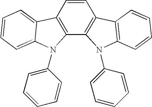
WO07063796 
WO07063754 5-member ring electron deficient heterocycles (e.g., triazole, oxadiazole) 
J. Appl. Phys. 90, 5048 (2001) 
WO04107822 Metal phenoxypyridine compounds 
WO05030900 Blue Hosts Arylcarbazoles 
Appl. Phys. Lett, 82, 2422 (2003) 
US20070190359 Dibenzothiophene-carbazole compounds 
WO2006114966 Phosphorescent dopants Red dopants Heavy metal porphyrins (e.g., PtOEP) 
Nature 395, 151 (1998) Iridium(III) organometallic complexes 
Appl. Phys. Lett. 78, 1622 (2001) 
U.S. Pat. No. 6,835,469 
U.S. Pat. No. 6,835,469 
US20060202194 
US20060202194 
U.S. Pat. No. 7,087,321 
U.S. Pat. No. 7,087,321 
Adv. Mater. 19, 739 (2007) Platinum(II) organometallic complexes 
WO2003040257 Osminum(III) complexes 
Chem. Mater. 17, 3532 (2005) Ruthenium(II) complexes 
Adv. Mater. 17, 1059 (2005) Green dopants Iridium(III) organometallic complexes 
Inorg. Chem. 40, 1704 (2001) 
US2002034656 
U.S. Pat. No. 6,687,266 
Chem. Mater. 16, 2480 (2004) 
US2007190359 
US 2006008670 JP2007123392 
Adv. Mater. 16, 2003 (2004) 
Angew. Chem. Int. Ed. 2006, 45, 7800 Pt(II) organometallic complexes 
Appl. Phys. Lett. 86, 153505 (2005) 
Appl. Phys. Lett. 86, 153505 (2005) 
Chem. Lett. 34, 592 (2005) Gold complexes 
Chem. Commun. 2906 (2005) Rhenium(III) complexes 
Inorg. Chem. 42, 1248 (2003) Blue dopants Iridium(III) organometallic complexes 
WO2002002714 
WO2006009024 
US2006251923 
WO2006056418, US2005260441 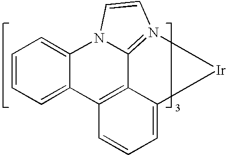
US2007190359 
US2002134984 
Angew. Chem. Int. Ed. 47, 1 (2008) 
Chem. Mater. 18, 5119 (2006) 
Inorg. Chem. 46, 4308 (2007) 
WO05123873 
WO05123873 
WO07004380 
WO06082742 Osmium(II) complexes 
US2005260449 
Organometallics 23, 3745 (2004) Gold complexes 
Appl. Phys. Lett. 74, 1361 (1999) Platinum(II) complexes 
WO06098120, WO06103874 Exciton/hole blocking layer materials Bathocuprine compounds (e.g., BCP, BPhen) 
Appl. Phys. Lett. 75, 4 (1999) 
Appl. Phys. Lett. 79, 449 (2001) Metal 8-hydroxyquinolates (e.g., BAlq) 
Appl. Phys. Lett. 81, 162 (2002) 5-member ring electron deficient heterocycles such as triazole, oxadiazole, imidazole, benzoimidazole 
Appl. Phys. Lett. 81, 162 (2002) Triphenylene compounds 
US20050025993 Fluorinated aromatic compounds 
Appl. Phys. Lett. 79, 156 (2001) Electron transporting materials Anthracene-benzoimidazole compounds 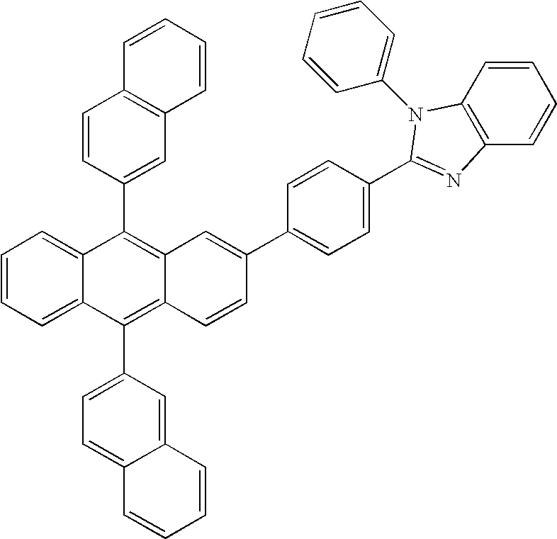
WO03060956 Anthracene-benzothiazole compounds 
Appl. Phys. Lett. 89, 063504 (2006) Metal 8-hydroxyquinolates (e.g., Alq3) 
Appl. Phys. Lett. 51, 913 (1987) Metal hydroxybenoquinolates 
Chem. Lett. 5, 905 (1993) Bathocuprine compounds such as BCP, BPhen, etc 
Appl. Phys. Lett. 91, 263503 (2007) 
Appl. Phys. Lett. 79, 449 (2001) 5-member ring electron deficient heterocycles (e.g., triazole, oxadiazole, imidazole, benzoimidazole) 
Appl. Phys. Lett. 74, 865 (1999) 
Appl. Phys. Lett. 55, 1489 (1989) 
Jpn. J. Apply. Phys. 32, L917 (1993) Silole compounds 
Org. Electron. 4, 113 (2003) Arylborane compounds 
J. Am. Chem. Soc. 120, 9714 (1998) Fluorinated aromatic compounds 
J. Am. Chem. Soc. 122, 1832 (2000) -
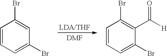
- Into a 1000 mL 3-neck flask equipped with magnetic stirring, a condenser and a thermocouple was charged with 100 mL of 2.0 M Lithium diisopropylamide (LDA) in THF. This solution was cooled to −75° C. Next, 1,3-Dibromobenzene (39.3 g, 0.167 mol) dissolved in 200 mL of anhydrous THF was added dropwise over a ½ h period to the cooled solution of LDA. The internal temperature was maintained at −75° C. (+/−5° C.) for 2 h. Next, dimethylformamide (30.8 g, 0.4 mol) dissolved in 50 mL of anhydrous THF and was added dropwise to the cooled reaction mixture over a ½ h period. The internal temperature was maintained at −75° C. (+/−5° C.) for 2 h. The reaction mixture was quenched by dropwise addition of 100 mL of 5% sulfuric acid. The cooling bath was removed and the reaction mixture was allowed to warm to room temperature. The organic layer was separated and the aqueous was extracted with 1×100 mL of diethyl ether and 1×50 mL of ethyl acetate. The organics were combined and washed 1×100 mL of brine. The organic extracts were then dried over sodium sulfate, filtered and concentrated under vacuum. The crude product was recrystallized from hexanes to yield 21.6 g (49% yield) of product.
-

- (Methoxymethyl)triphenylphosphonium chloride (34.3 g, 0.10 mol) was charged into a 500 mL 3-neck flask with 75 mL of THF. This solution was cooled to −78° C. followed by dropwise addition of 100 mL (0.1 mol) of 1.0 M of lithium bis(trimethylsilyl)amide in THF. Addition time was approximately 20 minutes and the internal temperature was maintained at −78° C. to −70° C. The cooling bath was then removed and the reaction mixture was allowed to warm to 0 to 3° C. The reaction mixture was then cooled back down to −78° C. Next, 2,6-dibromobenzaldehyde (22.8 g, 0.086 mol) dissolved in 75 mL of THF was added dropwise to the cooled reaction mixture over a 20 min period. The internal temperature was maintained between at −78° C. to −70° C. The reaction mixture was then allowed to gradually warm to room temperature. The reaction mixture was quenched with aqueous ammonium chloride and then extracted with 3×300 mL of ethyl acetate. The organic extracts were combined, washed once with 200 mL of 10% LiCl solution and were dried over magnesium sulfate. The extracts were then filtered and the solvent removed under vacuum. The crude product was purified by vacuum distillation to yield 22.5 g (90%) of product as a light-orange oil.
-

- 70 mL of conc. HCl was slowly added to a 500 mL round bottom flask containing 110 mL of water. o-Methyl 2,6-dibromophenylacetaldehyde (22.5 g, 0.077 mol) was dissolved in 70 mL of 1,4-dioxane and this solution was added all at once to the 500 mL round bottom flask. The reaction mixture was stirred and heated at a gentle reflux for 18 h. The reaction mixture was cooled to room temperature and was extracted with 2×400 mL ethyl acetate. These extracts were combined and were washed with 1×100 mL aq. 10% LiCl. The extracts were then dried over sodium sulfate, filtered and the solvent removed under vacuum. The 2,6-dibromophenyl acetaldehyde was purified using silica gel chromatography with 15%/75% methylene chloride/hexanes as the eluent. 17.1 g (80% yield) of white solids was obtained as the product.
-

- To a 200 mL round bottom flask was added 3.75 g (0.013 mol) of the 2,6-dibromophenylacetaldehyde, 30 mL of methylene chloride and 60 mL of 1,4-dioxane. Next, 2.32 g, (0.014 mol) of bromine was dissolved in 30 mL of methylene chloride and was added dropwise to the reaction mixture at room temperature over a 10 min period. Stirring was continued at room temperature for 2 h. An additional (0.23 g, 0.001 mol) of bromine was added to the reaction mixture. This mixture was stirred for one hour at room temperature. The reaction mixture was concentrated under vacuum. The crude product was then dissolved in 50 mL of diethyl ether and was washed 1×50 mL aqueous sodium bisulfite and 1×50 mL aqueous 10% lithium chloride. The ethereal extract was dried over sodium sulfate then was filtered and the solvent removed under vacuum to yield 4.2 g (90% yield) of a yellow viscous oil as the product which was immediately used for the next step.
-

- To a 1 L 3-neck flask was added 19 g (0.11 mol) of 2-bromoaniline, 27.7 g (0.12 mol) of 2-cyanophenylboronic acid pinacol ester, 74.5 g (0.32 mol) of potassium phosphate tribasic monohydrate and 1.8 g (0.002 mol) of [1,1′-bis[(diphenylphosphino)ferrocene]dichoro-palladium(II) complex with dichloromethane (1:1). This mixture was degassed and backfilled with nitrogen. Next, water (13 mL) and 350 mL of 1,4-dioxane were added to the reaction mixture and the degassing procedure was repeated. The reaction mixture was stirred and heated under nitrogen at reflux for 18 h. After cooling, the reaction mixture was diluted with 350 mL of water. The reaction mixture was extracted with 3×250 mL of ethyl acetate. These extracts were combined and dried over magnesium sulfate. The extracts were filtered and the solvent removed under vacuum. The crude product was triturated with a hexane/ethyl acetate mixture. A light gray solid was isolated via filtration.
-

- A 200 mL round bottom flask was charged with 0.77 g (0.004 mol) of 6-aminophenanthridine and 50 mL of anhydrous 2-propanol. To this mixture was added 1.42 g (0.004 mol) of α-bromo-2,6-dibromophenylacetaldehyde all at once. This mixture was then heated at reflux for 24 h. Next, the reaction mixture was cooled to 60° C. and 0.67 g (0.008 mol) of sodium bicarbonate was added all at once. This mixture was then heated at reflux for 24 h. The reaction mixture was cooled to room temperature, diluted with 300 mL of water and then was extracted with 3×200 mL of ethyl acetate. These organic extracts were combined, were washed 1×100 mL of aqueous 10% LiCl, were dried over sodium sulfate, then were filtered and concentrated under vacuum. The crude product was purified by silica gel column chromatography (1-7% ethyl acetate/methylene) to yield 1 g (55% yield) of off-white solids as the product.
-

- To a 200 mL flask was added dibromide from Step 6 (2.34 g, 5.175 mmol), isopropenyl boronic acid pinacol ester (10.44 g, 62.1 mmol), palladium(II) acetate (0.17 g, 0.76 mmol), 2-dicyclohexylphosphino-2′,6′-dimethoxybiphenyl (0.62 g, 1.52 mmol), potassium phosphate tribasic monohydrate (5.96 g, 25.88 mmol), 122 mL of toluene and 122 mL of water. The reaction mixture was fully degassed by freezing-pump-thaw technique. The reaction was heated to reflux and stirred under a nitrogen atmosphere for 16 h. The reaction mixture was filtered through a pad of Celite. The toluene layer was separated and the aqueous was extracted once with 75 mL of toluene. The toluene extracts were combined, dried over sodium sulfate, then were filtered and concentrated under vacuum. The product was purified using silica gel chromatography with 1-8% ethyl acetate/methylene chloride as the eluent to give 1.7 g (87% yield) of product.
-

- 2,6-diisopropenylimidazophenanthridine (1.7 g, 4.6 mmol) was dissolved in 75 mL of toluene. This solution was added to a Parr hydrogenator vessel that was purged with N2 and contained 1.5 g of chlorotris(triphenylphosphine) rhodium(I). This vessel was placed on the Parr hydrogenator and the vessel was filled with hydrogen and evacuated (repeated a total of three times). The vessel was then filled with hydrogen to 45 psi. This mixture was reacted with shaking for 21 h. The solvent from the reaction mixture was removed under vacuum. The crude product was chromatographed using a silica gel column with 1-8% ethyl acetate/methylene chloride as the eluent to yield 1.65 g of product.
-

- To a 50 mL Schlenk tube was added the ligand from Step 8 (1.47 g, 3.88 mmol), Ir(acac)3 (0.38 g, 0.78 mmol) and tridecane (50 drops). The mixture was degassed and heated in a sand bath at 240° C.-250° C. with stirring under a nitrogen for 66 h. After cooling, the reaction mixture was dissolved with a mixture of solvent (CH2Cl2:hexanes=1:1) and subject to flash column chromatography with 1:1 CH2Cl2:hexanes as the eluent. The solid after column chromatography was recrystallized from a mixture of CH2Cl2 and methanol to yield 0.65 g (65%) of product.
- Synthesis of Compound 1
-

- Step 1: To a 200 mL flask was added dibromide (1.0 g, 2.2 mmol), isobutyl boronic acid (2.7 g, 26.5 mmol), Pd2(dba)3 (0.15 g, 0.16 mmol), 2-dicyclohexylphosphino-2′, 6′-dimethoxybiphenyl (0.27 g, 0.65 mmol), potassium phosphate tribasic monohydrate (8.7 g, 37.58 mmol) and 100 mL of toluene. The reaction mixture was fully degassed by freezing-pump-thaw technique. The reaction was heated to reflux and stirred under a nitrogen atmosphere for 16 h. The reaction mixture was filtered through a pad of Celite. The toluene layer was separated and the aqueous was extracted once with 75 mL of toluene. The toluene extracts were combined, dried over sodium sulfate, then were filtered and concentrated under vacuum. The product was purified using silica gel chromatography with 1-8% ethyl acetate/methylene chloride as the eluent to give 0.76 g of product (84% yield).
-

- Step 2: To a 50 mL Schlenk tube was added the ligand (2.8 g, 6.89 mmol), Ir(acac)3 (0.68 g, 1.38 mmol) and tridecane (50 drops). The mixture was degassed and heated in a sand bath at 240-250° C. with stirring under a nitrogen for 73 h. After cooling, the reaction mixture was dissolved with a mixture of solvent (CH2Cl2:hexanes=1:1) and subject to flash column chromatography with 1:1 CH2Cl2:hexanes as the eluent. The solid after column chromatography was recrystallized from a mixture of CH2Cl2 and methanol to yield 1.69 g (87%) of product.
- Synthesis of Compound 2
-

- Step 1: To a 200 mL flask was added the dibromide (4 g, 8.84 mmol), 1-cyclohexene boronic acid pinacol ester (18.37 g, 88.27 mmol), Pd(OAc)2 (1.98 g, 2.9 mmol), 2-dicyclohexylphosphino-2′,6′-dimethoxybiphenyl (2.4 g, 5.83 mmol), potassium phosphate tribasic monohydrate (10.18 g, 44.23 mmol), 100 mL of toluene and 100 mL of water. The reaction mixture was fully degassed by freezing-pump-thaw technique. The reaction was heated to reflux and stirred under a nitrogen atmosphere for 16 h. The reaction mixture was filtered through a pad of Celite. The toluene layer was separated from the filtrate. The aqueous layer was extracted with 75 mL of toluene. The toluene extracts were combined, dried over sodium sulfate, then were filtered and concentrated under vacuum. The crude product was purified by column chromatography with 1-4% ethyl acetate/methylene chloride as the eluent to yield 3.2 g of product.
-

- Step 2: 3.2 g (0.007 mol) of the cyclohexenyl compound was dissolved in 150 mL of toluene. This solution was added to a Parr hydrogenation vessel that was purged with nitrogen and was charged with 2.8 g of 10% palladium on activated carbon and 1.4 g of platinum, 5 wt % (dry basis) on activated carbon wet, Degussa type F101. This heterogeneous mixture was shaken on the Parr hydrogenator for 72 h. The reaction mixture was filtered through a pad of Celite. The toluene filtrate was concentrated under vacuum. The crude product was purified by column chromatography with 1-5% ethyl acetate/methylene chloride as the eluent to yield 3.1 g of product.
-

- Step 3: To a 50 mL Schlenk tube were added ligand (2.3 g, 5.08 mmol), Ir(acac)3 (0.5 g, 1.01 mmol and tridecane (50 drops). The mixture was degassed and heated in a sand bath with stirring under a nitrogen for 73 h. After cooling, the reaction mixture was dissolved with a mixture of solvent (CH2Cl2:hexanes=1:1) and subject to flash column chromatography with 1:1 CH2Cl2:hexanes as the eluent. The solid after column chromatography was recrystallized from a mixture of CH2Cl2 and methanol to yield 0.93 g (58%) of product.
- Synthesis of
Compound 3 -

- Step 1. To a 500 mL 3-neck flask was charged diisopropylamine (9.9 g, 0.098 mol) and 100 mL of THF. This solution was cooled to −78° C. and 45.6 mL, 0.073 mol of n-BuLi 1.6 M in hexanes were added to the cooled reaction mixture via syringe. This mixture was stirred for ½ h at −78° C., then cycloheptanone (6.0 g, 0.054 mol) in 30 mL of THF was added dropwise to the cooled reaction mixture. This solution was stirred at −78° C. for 2 h. A THF solution of N-phenyl-bis-trifluoromethane sulfonimide (21.2 g, 0.059 mol) was added dropwise to the cooled mixture. The mixture was then allowed to gradually warm to room temperature and was stirred overnight. The reaction mixture was quenched with aqueous ammonium chloride then was extracted 2×300 mL of ethyl acetate. The extracts were then dried over magnesium sulfate and were filtered and concentrated under vacuum. The crude product was chromatographed with 30-40% methylene chloride/hexanes as the eluent to yield 9.0 g (69% yield) of product.
-

- Step 2. PdCl2(PPh3)2 (1.722 g, 2.45 mmol), PPh3 (1.28 g, 4.9 mmol), bis(pinacolato)diboron (90.76 g, 357 mmol) and KOPh (16.2 g, 122.7 mmol) were added to a flask. The flask was flushed with nitrogen and then charged with toluene (300 mL) and the triflate (20 g, 81.8 mmol). The mixture was then stirred at 50° C. for 16 h. The reaction mixture was diluted with 200 mL of water. The toluene layer was separated. The aqueous layer was extracted 200 mL of toluene. The toluene extracts were combined, washed 100 mL of aqueous 10% lithium chloride, dried over magnesium sulfate, filtered and concentrated under vacuum. The crude product was distilled using a Kugelrohr distillation setup. The pot temperature was started at 85° C. and was increased to 115° C. This distilled mixture was chromatographed with 20-25% methylene chloride/hexanes as the eluent to yield 9.85 g (55% yield) of product.
-

-
Step 3. To a 500 mL round bottom flask was added the dibromide (4.7 g, 0.01 mol), the boronic acid pinacol ester (9.81 g, 0.0442 mol), Pd(OAc)2 (0.75 g, 0.0033 mol), dicyclohexylphosphino-2′,6′-dimethoxybiphenyl (2.73 g, 0.007 mol), potassium phosphate tribasic monohydrate (12.0 g, 0.052 mol), 200 mL of toluene and 75 mL of water. The reaction mixture was evacuated and back-filled with nitrogen. The reaction was then heated to reflux and stirred under a nitrogen atmosphere for 16 h. The mixture was filtered through a pad of Celite. The toluene layer was separated and the aqueous was extracted with 100 mL of toluene. The toluene portions were combined and dried over magnesium sulfate. This dried organic mixture was then filtered and concentrated under vacuum. The crude product was purified by silica gel chromatography. The first purification involved eluting the column with 1-4% ethyl acetate/methylene chloride. The second purification involved eluting the column with 2-12% ethyl acetate/hexanes. The yield was 4.1 g (82%). -

- Step 4. The alkenyl product from
Step 3 was dissolved in 200 mL of toluene and was charged into a Parr hydrogenation bottle containing 2.8 g of 10% Pd/C and 1.4 g of 5% Pt/C Degussa Type F101 RA/W. This mixture was placed on the Parr hydrogenator for 18 h. The reaction mixture was filtered through a pad of Celite and the pad was rinsed with 200 mL of toluene. The toluene filtrate was concentrated under vacuum. The crude product was purified by silica gel chromatography with 5-15% ethyl acetate/hexanes as the eluent. The product obtained (3.6 g, 0.0074 mol) was dissolved in THF and was cooled to −78° C. To this cooled solution was added 6.3 mL of 1.6M n-BuLi in hexanes via syringe over a 5 min period. The reaction mixture was stirred for an additional 5 min then was quenched by adding 50 mL of water dropwise. This mixture was warmed to room temperature then was extracted 2×150 mL ethyl acetate. These extracts were dried over magnesium sulfate then were filtered and concentrated under vacuum. These extracts were then passed through a neutral alumina (deactivated by the addition of 6% (w/w) water) column that was eluted with 20-70% methylene chloride/hexanes. The material was dissolved in 50 mL of methylene chloride and was stirred at room temperature for 18 h with 0.8 g of Si-TAAcoH and 0.8 g of Si-Thiourea. This mixture was then filtered, concentrated under vacuum and the resulting material was recrystallized from hexanes to yield 2.93 g (71% yield) of product. -

- Step 5. To a 50 mL Schlenk tube were added the ligand (2.93 g, 6.03 mmol), Ir(acac)3 (0.59 g, 1.205 mmol) and tridecane (50 drops). The mixture was degassed and heated in a sand bath with stirring under a nitrogen for 73 h. After cooling, the reaction mixture was dissolved with a mixture of solvent (CH2Cl2:hexanes=1:1) and subject to flash column chromatography with 1:1 CH2Cl2:hexanes as the eluent. The solid after column chromatography was re-crystallized from a mixture of CH2Cl2 and methanol to yield 1.18 g of product.
- Synthesis of Compound 4
-

- Step 1. 10.0 g (0.08 mol) of 4,4-dimethylcyclohex-2-enone was dissolved in 150 mL of ethanol. This solution was added to a Parr hydrogenation vessel that was purged with nitrogen and was charged with 0.5 g of 10% palladium on activated carbon. This heterogeneous mixture was shaken on the Parr hydrogenator for 8 h. The reaction mixture was filtered through Celite and evaporated to dryness to yield 7.9 g of product.
-

- Step 2. A mixture of p-tolylsulfonylhydrazine (6.8 g, 36.7 mmol), 60 mL of absolute ethanol and the ketone (4.64 g, 36.76 mmol) was heated to reflux at 100° C. After heating for 2 h, the reaction mixture was cooled using an ice-water bath to precipitate the majority of the hydrazone. The resulting solid was collected by filtration and was washed thoroughly with ice-cold ethanol. Air drying for 1 h afforded 7.67 g of the required hydrazone.
-

-
Step 3. To a dried 500 mL round-bottom flask equipped with a magnetic stirbar and rubber septum, hydrazone (5 g, 17 mmol) was added followed by 100 mL of anhydrous hexanes. To thismixture 100 mL of anhydrous TMEDA were added, and the reaction mixture was cooled to −78° C. and maintained at this temperature for 15 min, after which 60.6 mL (84.9 mmol) of 2.5M sec-BuLi was added over 15 min. The reaction mixture was then stirred for 1 h at −78° C. and then brought to room temperature and stirred for 1.5 h. The mixture was cooled down to −78° C. again and 15.8 g (84.9 mmol) of pinacol isopropyl borate was then added. The reaction was stirred for another hour at −78° C. and then brought to room temperature and stirred for 3 h. The reaction was quenched with the addition of saturated NH4Cl and then extracted three times with ether. The combined organic extracts were dried over anhydrous MgSO4, filtered, and concentrated in vacuo. The residue was subject to flash chromatography (40% CH2Cl2 in hexanes) to afford 1.53 g (38%) of desired product. -

- Step 4. To a 200 mL flask was added dibromide (5 g, 11.06 mmol), bornic acid pinacol ester from step 3 (11.26 g, 47.67 mmol), Pd(OAc)2 (819 mg, 3.64 mmol), dicyclohexylphosphino-2′,6′-dimethoxybiphenyl (2.9 g, 7.3 mmol), potassium phosphate tribasic monohydrate (12.73 g, 55.29 mmol), 150 mL of toluene and 150 mL of water. The reaction mixture was fully degassed by freezing-pump-thaw technique. The reaction was heated to reflux and stirred under a nitrogen atmosphere for 16 h. The reaction mixture was filtered through a pad of Celite. The toluene layer was separated from the filtrate. The aqueous layer was extracted 75 mL of toluene. The toluene extracts were combined, dried over sodium sulfate, then were filtered and concentrated under vacuum. The crude product was passed through a silica gel column. The column was eluted with 10% ethyl acetate in hexanes to yield 4.5 g of desired product.
-

- Step 5. 4.5 (8.81 mol) of the cyclohexenyl product from step 4 was dissolved in 150 mL of toluene. This solution was added to a Parr hydrogenation vessel that was purged with nitrogen and was charged with 3.2 g of 10% palladium on activated carbon and 2.8 g of Platinum, 5 wt % (dry basis) on activated carbon wet, Degussa type F101. This heterogeneous mixture was shaken on the Parr hydrogenator for 16 h. The reaction mixture was filtered through a pad of Celite. The toluene filtrate was concentrated under vacuum. The crude product was passed through a silica gel column. The column was eluted with 10% ethyl acetate in hexanes to yield 4.24 g of product.
-

- Step 6. To a 50 mL Schlenk tube were added ligand (2.57 g, 5.03 mmol), Ir(acac)3 (0.495 g, 1.006 mmol) and tridecane (50 drops). The mixture was degassed and heated in a sand bath with stirring under a nitrogen atmosphere for 73 h. After cooling, the reaction mixture was dissolved with a mixture of solvent (CH2Cl2:dexanes=1:1) and subject to flash column chromatography (CH2Cl2:dexanes=1:1). The solid after column chromatography was recrystallized from a mixture of CH2Cl2 and methanol to yield 0.8 g of product.
- Synthesis of Compound 5
-

- Step 1. A mixture of 4-tert-butylcyclohexanone (26.5 g, 0.172 mol), p-toluenesulfonylhydrazide (31.74 g, 0.171 mol) and 450 mL of anhydrous ethanol was heated to reflux for 4 h then cooled to room temperature. The reaction mixture was filtered and dried under vacuum to yield 35 g of product.
-

- Step 2. To a dried 500 mL round-bottom flask equipped with a magnetic stirbar and rubber septum, hydrazone (7.5 g, 0.023 mol) was added followed by 70 mL of anhydrous hexanes. To this mixture 70 mL of anhydrous TMEDA was added and the reaction mixture was cooled to −78° C. and maintained at this temperature for 15 min, after which 37 mL (0.092 mol) of 2.5M n-BuLi in hexanes were added over 15 min. The reaction mixture was then stirred for 1 h at −78° C. and then brought to room temperature and stirred for 3.5 h. The mixture was brought to −78° C. again and 17 g (0.092 mol) of pinacol isopropyl borate were added. The reaction was stirred for another hour at −78° C. and then brought to room temperature and stirred for overnight. The reaction was quenched with the addition of saturated NH4Cl and then was partitioned with 200 mL of ether. This heterogeneous mixture was passed through a Celite pad. The ether layer was separated and the aqueous was extracted 300 mL of ether. The combined organic extracts were dried over anhydrous MgSO4, filtered, and concentrated under vacuum. The crude product was passed through a silica gel column (20-40% methylene chloride/hexanes). 4.4 g (72% yield) of product was obtained.
-

-
Step 3. To a 1 L round bottom flask was added dibromide (5 g, 0.011 mol), boronic acid pinacol ester from step 2 (7.3 g, 0.0276 mol), tris(dibenzylideneacetone)dipalladium(0) (0.2 g, 0.22 mmol), dicyclohexylphosphino-2′,6′-dimethoxybiphenyl (0.36 g, 0.88 mmol), potassium phosphate tribasic monohydrate (14.0 g, 0.066 mol), 300 mL of toluene and 80 mL of water. The reaction mixture was evacuated and back-filled with nitrogen. The reaction was then heated to reflux and stirred under a nitrogen atmosphere for 16 h. The heterogeneous reaction mixture was filtered through a pad of Celite. The toluene layer was separated and the aqueous was extracted 100 mL of toluene. The toluene portions were combined and dried over magnesium sulfate. This dried organic mixture was then filtered and concentrated under vacuum. The crude product was purified by silica gel chromatography. The column was eluted with 1-4% ethyl acetate/methylene chloride. 5 g (80% yield) of product was obtained. -

- Step 4. The alkenyl product (5.0 g, 0.0088 mol) from
Step 3 was dissolved in 200 mL of toluene and was charged into a Parr hydrogenation bottle that already contained 3.8 g of 10% Pd/C and 3.0 g of 5% Pt/C Degussa Type F101 RA/W. This mixture was placed on the Parr hydrogenator for 58 h. The reaction mixture was filtered through a pad of Celite and the pad was rinsed with 200 mL of toluene. The toluene filtrate was concentrated under vacuum to yield 4.3 g of crude product. The crude product was purified by silica gel chromatography. The column was eluted with 1-5% ethyl acetate/methylene chloride. Next, the product obtained from the column was dissolved in 50 mL of methylene chloride and was stirred at room temperature for 18 h with 1.1 g of Si-TAAcoH and 1.1 g of Si-Thiourea. This is to remove any residual palladium. The product obtained (3.9 g, 0.0068 mol) was dissolved in THF and was cooled to −78° C. To this cooled solution was added 5.8 mL of 1.6 M n-BuLi in hexanes via syringe over a 5 min period. The reaction mixture was stirred for an additional 5 minutes then was quenched by adding 50 mL of water dropwise. This mixture was warmed to room temperature then was extracted 2×150 mL ethyl acetate. These extracts were dried over magnesium sulfate then were filtered and concentrated under vacuum. These extracts were then passed through a neutral alumina (deactivated by the addition of 6% (w/w) water) column that was eluted with 30-60% methylene chloride/hexanes. 3.6 g of product was obtained. The product obtained from the neutral alumina column was recrystallized from hexanes/ethyl acetate. 2.90 g of product was obtained. -

- Step 5. To a 50 mL Schlenk tube were added ligand (2.78 g, 4.86 mmol), Ir(acac)3 (0.478 g, 0.97 mmol) and tridecane (50 drops). The mixture was degassed and heated in a sand bath with stirring under a nitrogen for 70 h. After cooling, the reaction mixture was dissolved with a mixture of solvent (CH2Cl2:dexanes=1:1) and subject to flash column chromatography CH2Cl2:hexanes=1:1). The solid after column chromatography was recrystallized from a mixture of CH2Cl2 and methanol to yield 1.0 g of product.
- All device examples were fabricated by high vacuum (<10−7 Torr) thermal evaporation. The anode electrode is 1200 Å of indium tin oxide (ITO). The cathode consisted of 10 Å of LiF followed by 1000 Å of Al. All devices were encapsulated with a glass lid sealed with an epoxy resin in a nitrogen glove box (<1 ppm of H2O and O2) immediately after fabrication, and a moisture getter was incorporated inside the package.
- The organic stack of the Device Examples 1 and 2 in Table 2, consisted of sequentially, from the ITO surface, 10 nm of H3 or H4 as the hole injection layer (HIL), 30 nm of 4,4′-bis[N-(1-naphthyl)-N-phenylamino]biphenyl (α-NPD) as the hole transporting later (HTL), 30 nm of the H2 doped with 9% of the dopant emitter (e.g., invention Compounds 1-2) as the emissive layer (EML), 5 nm of H2 as the ETL2 and 40 nm of Alq as ETL1.
- Comparative Examples 1-3 were fabricated similarly to the Device Examples except E1, E2, or E3 was used as the emissive dopant and H1 was used as the host in the EML and as the ETL2 material.
- As used herein, the following compounds have the following structures:
-


- Particular emissive dopants for the emissive layer of an OLED are provided which may lead to devices having particularly good properties. The device structure and the results from device testing are provided in Table 2. Devices having an emissive layer using Compounds 1 and 2 as the emissive dopant show improved device efficiency and stability as well as improved color indicating that these substituted imidazophenanthridine compounds may be beneficial.
- Solid state photoluminescent quantum yields (PL %) were determined from 1 weight % of the dopant in polymethylmethacrylate (PMMA), an optically inert polymer matrix. The samples are prepared by dissolving the dopant and PMMA in 1 mL of toluene per 100 mg solids (90 mg of PMMA and 10 mg of the dopant). The samples were filtered and drop-casted onto a pre-cleaned quartz substrate. After the solvent has evaporated, PL quantum yields were measured using a Hamamatsu Absolute PL Quantum Yield Measurement System. The system is comprised of an integrating sphere, xenon light source, monochromater, and multi-channel CCD spectrometer, and is housed in an inert atmosphere glove box to prevent quenching by oxygen. The excitation wavelength was 342 nm.
-
TABLE 2 EQE (%) V (V) T1/2 (h) Device Emitter at 1000 at 1000 at 2000 Sublimation Example (doping %) cd/m2 cd/m2 cd/m2 CIE temp. (° C.) HIL HOST ETL2 PL % Comparative E1 (9) 12 8 70 0.15, 0.23 330 H3 H1 H1 52 1 Comparative E2 (9) 7 8 200 0.15, 0.24 300 H4 H1 H1 26 2 Comparative E3 (9) 8 8 180 0.15, 0.26 320 H4 H1 H1 40 3 1 1 (9) 12 7 200 0.15, 0.24 265 H3 H2 H2 56 2 2 (9) 12 8 300 0.15, 0.23 310 H4 H2 H2 60 - From Device Examples 1 and 2, it can be seen that the device efficiencies correlate with the solid state PL quantum yields. Comparative Example 1 gives a higher PL efficiency compared to Comparative Example 2. It is believed that the alkyl substitution present in E1 used in Comparative Example 1 inhibits self quenching leading to higher PL and EL efficiencies. Comparative Example 2 uses E2 which has 2,6-dimethyl twisted aryl groups and relatively low PL quantum efficiencies. In these cases the 2,6 alkyl substitutions are not bulky enough to inhibit self quenching. Furthermore, Comparative example 3 uses E3 which has a bulky neopentyl group substituted on the other ring of the ligand, yet this does not lead to a large improvement in PL quantum yield. Compounds 1 and 2 with bulky alkyl groups substituted to the twisted aryl are found to have higher PL quantum yield and therefore improved device efficiency. Alkyl groups particularly beneficial as these lead to minimal red-shifting. The use of bulky alkyl substituents (i.e., alkyl groups containing four or more atoms) is believed to be a novel way to modify the compound to inhibit self quenching. These bulky substituted compounds do not suffer the lifetime limitation of compounds having alkyl groups substituted to the 4-imidazole position, as seen for E1 used in Comparative Example 1.
- Attaching a methyl group to the 2 position of the imidazophenanthridine, as shown for E1 in Comparative example 1, increased solid state quantum yield of the dopant and lead to higher device efficiency. However, several examples demonstrated that the addition of alkyl substituents at this position can lead to devices having short lifetimes (i.e., less than 100 hours at 2000 nits). Alternatively, it was found that attaching bulky alkyl groups (i.e., alkyls having four or more atoms) increased photoluminescent efficiency and device efficiency. For example, Compounds 1 and 2 have high efficiency, similar to Comparative example 1, and greater efficiency than Comparative examples 2 and 3. Both the selection of bulky alkyl substituents and the site of substitution (i.e., 2 and/or n position of the twisted aryl) may be important to obtain the increased efficiency. For example, E3 used in Comparative example 3 has a bulky neopentyl group substituted away from the imidazole, yet this compound has a relatively low PL yield of 40%. Notably, the compounds provided herein demonstrate significantly long device lifetimes. For example, the device lifetime of invention Compounds 1 and 2 are 3-4 times longer when compared to Comparative example 1. Bulky alkyl substitution on the twisted aryl may also improve device processing. For example, Compound 1 has an isobutyl substitution and has a sublimation temperature of 265° C., which is the lowest sublimation temperature to be observed to date in this family of imidazo[1,2-f]phenanthridine iridium complexes.
- It is understood that the various embodiments described herein are by way of example only, and are not intended to limit the scope of the invention. For example, many of the materials and structures described herein may be substituted with other materials and structures without deviating from the spirit of the invention. The present invention as claimed may therefore includes variations from the particular examples and preferred embodiments described herein, as will be apparent to one of skill in the art. It is understood that various theories as to why the invention works are not intended to be limiting.
Claims (20)


Priority Applications (14)
| Application Number | Priority Date | Filing Date | Title |
|---|---|---|---|
| US12/632,251 US8815415B2 (en) | 2008-12-12 | 2009-12-07 | Blue emitter with high efficiency based on imidazo[1,2-f] phenanthridine iridium complexes |
| EP16166849.6A EP3081617B1 (en) | 2008-12-12 | 2009-12-11 | Blue emitter with high efficiency based on imidazo [1,2-f] phenanthridine iridium complexes |
| TW098142607A TWI492945B (en) | 2008-12-12 | 2009-12-11 | Blue emitter with high efficiency based on imidazo(1,2-f)phenanthridine iridium complexes |
| TW104112487A TWI580680B (en) | 2008-12-12 | 2009-12-11 | Blue emitter with high efficiency based on imidazo[1,2-f]phenanthridine iridium complexes |
| CN201410120954.6A CN103896991B (en) | 2008-12-12 | 2009-12-11 | Efficient blue light-emitting body is had based on imidazo [1,2 f] phenanthridines complex of iridium |
| PCT/US2009/067687 WO2010068876A1 (en) | 2008-12-12 | 2009-12-11 | BLUE EMITTER WITH HIGH EFFICIENCY BASED ON IMIDAZO [1,2-f] PHENANTHRIDINE IRIDIUM COMPLEXES |
| EP09796526.3A EP2382281B1 (en) | 2008-12-12 | 2009-12-11 | BLUE EMITTER WITH HIGH EFFICIENCY BASED ON IMIDAZO [1,2-f] PHENANTHRIDINE IRIDIUM COMPLEXES |
| CN200980155336.2A CN102292409B (en) | 2008-12-12 | 2009-12-11 | Blue emitter with high efficiency based on imidazo [1,2-f] phenanthridine iridium complexes |
| JP2011540925A JP6258570B2 (en) | 2008-12-12 | 2009-12-11 | Blue emitter with high efficiency based on imidazo [1,2-f] phenanthridine iridium complex |
| KR1020117016181A KR101636100B1 (en) | 2008-12-12 | 2009-12-11 | BLUE EMITTER WITH HIGH EFFICIENCY BASED ON IMIDAZO [1,2-f] PHENANTHRIDINE IRIDIUM COMPLEXES |
| US14/330,351 US10008678B2 (en) | 2008-12-12 | 2014-07-14 | Organic electroluminescent materials and devices |
| JP2016100224A JP6506211B2 (en) | 2008-12-12 | 2016-05-19 | Blue emitter with high efficiency based on imidazo [1,2-f] phenanthridine iridium complex |
| JP2017195003A JP6586140B2 (en) | 2008-12-12 | 2017-10-05 | Blue emitter with high efficiency based on imidazo [1,2-f] phenanthridine iridium complex |
| JP2019100281A JP6763999B2 (en) | 2008-12-12 | 2019-05-29 | Highly efficient blue illuminant based on imidazole [1,2-f] phenanthridine iridium complex |
Applications Claiming Priority (2)
| Application Number | Priority Date | Filing Date | Title |
|---|---|---|---|
| US12225908P | 2008-12-12 | 2008-12-12 | |
| US12/632,251 US8815415B2 (en) | 2008-12-12 | 2009-12-07 | Blue emitter with high efficiency based on imidazo[1,2-f] phenanthridine iridium complexes |
Related Child Applications (1)
| Application Number | Title | Priority Date | Filing Date |
|---|---|---|---|
| US14/330,351 Continuation US10008678B2 (en) | 2008-12-12 | 2014-07-14 | Organic electroluminescent materials and devices |
Publications (2)
| Publication Number | Publication Date |
|---|---|
| US20100148663A1 true US20100148663A1 (en) | 2010-06-17 |
| US8815415B2 US8815415B2 (en) | 2014-08-26 |
Family
ID=42239674
Family Applications (2)
| Application Number | Title | Priority Date | Filing Date |
|---|---|---|---|
| US12/632,251 Active 2031-07-07 US8815415B2 (en) | 2008-12-12 | 2009-12-07 | Blue emitter with high efficiency based on imidazo[1,2-f] phenanthridine iridium complexes |
| US14/330,351 Active 2032-06-17 US10008678B2 (en) | 2008-12-12 | 2014-07-14 | Organic electroluminescent materials and devices |
Family Applications After (1)
| Application Number | Title | Priority Date | Filing Date |
|---|---|---|---|
| US14/330,351 Active 2032-06-17 US10008678B2 (en) | 2008-12-12 | 2014-07-14 | Organic electroluminescent materials and devices |
Country Status (7)
| Country | Link |
|---|---|
| US (2) | US8815415B2 (en) |
| EP (2) | EP3081617B1 (en) |
| JP (4) | JP6258570B2 (en) |
| KR (1) | KR101636100B1 (en) |
| CN (2) | CN103896991B (en) |
| TW (2) | TWI580680B (en) |
| WO (1) | WO2010068876A1 (en) |
Cited By (84)
| Publication number | Priority date | Publication date | Assignee | Title |
|---|---|---|---|---|
| KR20130018738A (en) * | 2010-03-03 | 2013-02-25 | 유니버셜 디스플레이 코포레이션 | Phosphorescent materials |
| US20130049576A1 (en) * | 2011-08-25 | 2013-02-28 | Konica Minolta Holdings, Inc. | Organic electroluminescence element, lighting device and display device |
| US8471037B2 (en) | 2011-08-12 | 2013-06-25 | Industrial Technology Research Institute | Derivatives having vinyl group and its use in electroluminescent element |
| US20130228758A1 (en) * | 2012-03-01 | 2013-09-05 | Vivian Wing Wah Yam | Dendrimers Containing Luminescent Gold (III) Compounds for Organic Light-Emitting Devices and Their Preparation |
| US20140027716A1 (en) * | 2012-07-25 | 2014-01-30 | Universal Display Corporation (027166) | Heteroleptic cyclometallated ir(iii) complexes having a cyclometallated 6-membered ring |
| US8716484B1 (en) | 2012-12-05 | 2014-05-06 | Universal Display Corporation | Hole transporting materials with twisted aryl groups |
| US8889864B2 (en) | 2006-02-10 | 2014-11-18 | Universal Display Corporation | Metal complexes of cyclometallated imidazo[1,2-f]phenanthridine and diimidazo[1,2-a:1′,2′-c]quinazoline ligands and isoelectronic and benzannulated analogs thereof |
| US9054344B2 (en) | 2010-01-20 | 2015-06-09 | Universal Display Corporation | Electroluminescent devices for lighting applications |
| US9196860B2 (en) | 2012-12-04 | 2015-11-24 | Universal Display Corporation | Compounds for triplet-triplet annihilation upconversion |
| US9236580B2 (en) | 2011-10-19 | 2016-01-12 | E I Du Pont De Nemours And Company | Organic electronic device for lighting |
| US9252363B2 (en) | 2012-10-04 | 2016-02-02 | Universal Display Corporation | Aryloxyalkylcarboxylate solvent compositions for inkjet printing of organic layers |
| EP3056504A1 (en) | 2015-02-16 | 2016-08-17 | Universal Display Corporation | Organic electroluminescent materials and devices |
| EP3061763A1 (en) | 2015-02-27 | 2016-08-31 | Universal Display Corporation | Organic electroluminescent materials and devices |
| US9450198B2 (en) | 2014-04-15 | 2016-09-20 | Universal Display Corporation | Organic electroluminescent materials and devices |
| EP3098229A1 (en) | 2015-05-15 | 2016-11-30 | Universal Display Corporation | Organic electroluminescent materials and devices |
| EP3101021A1 (en) | 2015-06-01 | 2016-12-07 | Universal Display Corporation | Organic electroluminescent materials and devices |
| EP3124488A1 (en) | 2015-07-29 | 2017-02-01 | Universal Display Corporation | Organic electroluminescent materials and devices |
| EP3159350A1 (en) | 2015-09-03 | 2017-04-26 | Universal Display Corporation | Organic electroluminescent materials and devices |
| US9653691B2 (en) | 2012-12-12 | 2017-05-16 | Universal Display Corporation | Phosphorescence-sensitizing fluorescence material system |
| EP3205658A1 (en) | 2016-02-09 | 2017-08-16 | Universal Display Corporation | Organic electroluminescent materials and devices |
| EP3231809A2 (en) | 2016-04-11 | 2017-10-18 | Universal Display Corporation | Organic electroluminescent materials and devices |
| EP3261146A2 (en) | 2016-06-20 | 2017-12-27 | Universal Display Corporation | Organic electroluminescent materials and devices |
| EP3261147A1 (en) | 2016-06-20 | 2017-12-27 | Universal Display Corporation | Organic electroluminescent materials and devices |
| EP3270435A2 (en) | 2016-06-20 | 2018-01-17 | Universal Display Corporation | Organic electroluminescent materials and devices |
| US9876173B2 (en) | 2013-12-09 | 2018-01-23 | Universal Display Corporation | Organic electroluminescent materials and devices |
| EP3297051A1 (en) | 2016-09-14 | 2018-03-21 | Universal Display Corporation | Organic electroluminescent materials and devices |
| EP3301088A1 (en) | 2016-10-03 | 2018-04-04 | Universal Display Corporation | Condensed pyridines as organic electroluminescent materials and devices |
| EP3305796A1 (en) | 2016-10-07 | 2018-04-11 | Universal Display Corporation | Organic electroluminescent materials and devices |
| EP3321258A1 (en) | 2016-11-09 | 2018-05-16 | Universal Display Corporation | 4-phenylbenzo[g]quinazoline or 4-(3,5-dimethylphenylbenzo[g]quinazoline iridium complexes for use as near-infrared or infrared emitting materials in oleds |
| EP3323822A1 (en) | 2016-09-23 | 2018-05-23 | Universal Display Corporation | Organic electroluminescent materials and devices |
| EP3345914A1 (en) | 2017-01-09 | 2018-07-11 | Universal Display Corporation | Organic electroluminescent materials and devices |
| EP3354654A2 (en) | 2016-11-11 | 2018-08-01 | Universal Display Corporation | Organic electroluminescent materials and devices |
| EP3381927A1 (en) | 2017-03-29 | 2018-10-03 | Universal Display Corporation | Organic electroluminescent materials and devices |
| EP3401318A1 (en) | 2017-05-11 | 2018-11-14 | Universal Display Corporation | Organic electroluminescent materials and devices |
| EP3418286A1 (en) | 2017-06-23 | 2018-12-26 | Universal Display Corporation | Organic electroluminescent materials and devices |
| EP3444258A2 (en) | 2017-08-10 | 2019-02-20 | Universal Display Corporation | Organic electroluminescent materials and devices |
| US10276805B2 (en) * | 2014-05-08 | 2019-04-30 | Universal Display Corporation | Organic electroluminescent materials and devices |
| EP3489243A1 (en) | 2017-11-28 | 2019-05-29 | University of Southern California | Carbene compounds and organic electroluminescent devices |
| EP3492528A1 (en) | 2017-11-30 | 2019-06-05 | Universal Display Corporation | Organic electroluminescent materials and devices |
| EP3492480A2 (en) | 2017-11-29 | 2019-06-05 | Universal Display Corporation | Organic electroluminescent materials and devices |
| EP3613751A1 (en) | 2018-08-22 | 2020-02-26 | Universal Display Corporation | Organic electroluminescent materials and devices |
| US10636983B2 (en) | 2014-05-08 | 2020-04-28 | Universal Display Corporation | Organic electroluminescent materials and devices |
| DE102013200085B4 (en) | 2012-01-06 | 2020-06-18 | Universal Display Corporation | Highly efficient phosphorescent materials |
| EP3689889A1 (en) | 2019-02-01 | 2020-08-05 | Universal Display Corporation | Organic electroluminescent materials and devices |
| EP3690973A1 (en) | 2019-01-30 | 2020-08-05 | University Of Southern California | Organic electroluminescent materials and devices |
| EP3715353A1 (en) | 2019-03-26 | 2020-09-30 | Universal Display Corporation | Organic electroluminescent materials and devices |
| US20200354390A1 (en) * | 2019-05-07 | 2020-11-12 | Universal Display Corporation | Organic electroluminescent materials and devices |
| EP3750897A1 (en) | 2019-06-10 | 2020-12-16 | Universal Display Corporation | Organic electroluminescent materials and devices |
| US10873027B2 (en) * | 2012-12-11 | 2020-12-22 | Nissan Chemical Industries, Ltd. | Process for the manufacture of a multilayer structure |
| EP3771717A1 (en) | 2019-07-30 | 2021-02-03 | Universal Display Corporation | Organic electroluminescent materials and devices |
| EP3778614A1 (en) | 2019-08-16 | 2021-02-17 | Universal Display Corporation | Organic electroluminescent materials and devices |
| EP3816175A1 (en) | 2019-11-04 | 2021-05-05 | Universal Display Corporation | Organic electroluminescent materials and devices |
| EP3845545A1 (en) | 2020-01-06 | 2021-07-07 | Universal Display Corporation | Organic electroluminescent materials and devices |
| EP3858945A1 (en) | 2020-01-28 | 2021-08-04 | Universal Display Corporation | Organic electroluminescent materials and devices |
| EP3937268A1 (en) | 2020-07-10 | 2022-01-12 | Universal Display Corporation | Plasmonic oleds and vertical dipole emitters |
| WO2022058523A1 (en) | 2020-09-18 | 2022-03-24 | Cynora Gmbh | Organic electroluminescent device emitting blue light |
| EP4001287A1 (en) | 2020-11-24 | 2022-05-25 | Universal Display Corporation | Organic electroluminescent materials and devices |
| EP4001286A1 (en) | 2020-11-24 | 2022-05-25 | Universal Display Corporation | Organic electroluminescent materials and devices |
| EP4016659A1 (en) | 2020-11-16 | 2022-06-22 | Universal Display Corporation | Organic electroluminescent materials and devices |
| EP4019526A1 (en) | 2018-01-26 | 2022-06-29 | Universal Display Corporation | Organic electroluminescent materials and devices |
| EP4039692A1 (en) | 2021-02-03 | 2022-08-10 | Universal Display Corporation | Organic electroluminescent materials and devices |
| EP4053137A1 (en) | 2021-03-05 | 2022-09-07 | Universal Display Corporation | Organic electroluminescent materials and devices |
| EP4056578A1 (en) | 2021-03-12 | 2022-09-14 | Universal Display Corporation | Organic electroluminescent materials and devices |
| EP4060758A2 (en) | 2021-02-26 | 2022-09-21 | Universal Display Corporation | Organic electroluminescent materials and devices |
| EP4059915A2 (en) | 2021-02-26 | 2022-09-21 | Universal Display Corporation | Organic electroluminescent materials and devices |
| EP4059941A1 (en) | 2021-03-15 | 2022-09-21 | Universal Display Corporation | Organic electroluminescent materials and devices |
| EP4075531A1 (en) | 2021-04-13 | 2022-10-19 | Universal Display Corporation | Plasmonic oleds and vertical dipole emitters |
| EP4074723A1 (en) | 2021-04-05 | 2022-10-19 | Universal Display Corporation | Organic electroluminescent materials and devices |
| EP4075530A1 (en) | 2021-04-14 | 2022-10-19 | Universal Display Corporation | Organic electroluminescent materials and devices |
| EP4079743A1 (en) | 2021-04-23 | 2022-10-26 | Universal Display Corporation | Organic electroluminescent materials and devices |
| EP4086266A1 (en) | 2021-04-23 | 2022-11-09 | Universal Display Corporation | Organic electroluminescent materials and devices |
| EP4112701A2 (en) | 2021-06-08 | 2023-01-04 | University of Southern California | Molecular alignment of homoleptic iridium phosphors |
| DE102013214144B4 (en) | 2012-07-19 | 2023-02-16 | Universal Display Corp. | Diarylamino-substituted metal complexes |
| EP4151699A1 (en) | 2021-09-17 | 2023-03-22 | Universal Display Corporation | Organic electroluminescent materials and devices |
| EP4185086A1 (en) | 2017-07-26 | 2023-05-24 | Universal Display Corporation | Organic electroluminescent materials and devices |
| EP4212539A1 (en) | 2021-12-16 | 2023-07-19 | Universal Display Corporation | Organic electroluminescent materials and devices |
| DE102013003605B4 (en) | 2012-03-15 | 2023-08-17 | Universal Display Corporation | Secondary hole transport layer with tricarbazole compounds |
| EP4231804A2 (en) | 2022-02-16 | 2023-08-23 | Universal Display Corporation | Organic electroluminescent materials and devices |
| EP4242285A1 (en) | 2022-03-09 | 2023-09-13 | Universal Display Corporation | Organic electroluminescent materials and devices |
| EP4265626A2 (en) | 2022-04-18 | 2023-10-25 | Universal Display Corporation | Organic electroluminescent materials and devices |
| EP4282863A1 (en) | 2022-05-24 | 2023-11-29 | Universal Display Corporation | Organic electroluminescent materials and devices |
| EP4293001A1 (en) | 2022-06-08 | 2023-12-20 | Universal Display Corporation | Organic electroluminescent materials and devices |
| EP4299693A1 (en) | 2022-06-28 | 2024-01-03 | Universal Display Corporation | Organic electroluminescent materials and devices |
| EP4326030A1 (en) | 2022-08-17 | 2024-02-21 | Universal Display Corporation | Organic electroluminescent materials and devices |
Families Citing this family (51)
| Publication number | Priority date | Publication date | Assignee | Title |
|---|---|---|---|---|
| US20100141125A1 (en) | 2007-05-16 | 2010-06-10 | Konica Minolta Holdings, Inc. | Organic electroluminescent element, display device and lighting device |
| JP5564942B2 (en) * | 2007-05-16 | 2014-08-06 | コニカミノルタ株式会社 | Organic electroluminescence element, display device and lighting device |
| US8815415B2 (en) * | 2008-12-12 | 2014-08-26 | Universal Display Corporation | Blue emitter with high efficiency based on imidazo[1,2-f] phenanthridine iridium complexes |
| JP5531446B2 (en) * | 2009-04-20 | 2014-06-25 | コニカミノルタ株式会社 | ORGANIC ELECTROLUMINESCENT ELEMENT, ORGANIC ELECTROLUMINESCENT ELEMENT MATERIAL, DISPLAY DEVICE AND LIGHTING DEVICE |
| JP5568889B2 (en) * | 2009-05-22 | 2014-08-13 | コニカミノルタ株式会社 | ORGANIC ELECTROLUMINESCENT ELEMENT, DISPLAY DEVICE, LIGHTING DEVICE, AND ORGANIC ELECTROLUMINESCENT ELEMENT MATERIAL |
| WO2011024737A1 (en) | 2009-08-27 | 2011-03-03 | 独立行政法人産業技術総合研究所 | Iridium complex and light emitting material formed from same |
| WO2012116231A2 (en) * | 2011-02-23 | 2012-08-30 | Universal Display Corporation | Novel tetradentate platinum complexes |
| CN105070846B (en) | 2011-03-23 | 2018-07-06 | 株式会社半导体能源研究所 | Light-emitting component, light-emitting device, lighting device and electronic equipment |
| US9783564B2 (en) * | 2011-07-25 | 2017-10-10 | Universal Display Corporation | Organic electroluminescent materials and devices |
| CN107573363A (en) | 2012-09-20 | 2018-01-12 | Udc 爱尔兰有限责任公司 | The azepine dibenzofurans of supplied for electronic application and the electronic device for including azepine dibenzofurans |
| EP2976793B1 (en) | 2013-03-20 | 2019-04-24 | UDC Ireland Limited | Use of azabenzimidazole carbene complexes in oleds |
| CN109438518B (en) | 2013-07-02 | 2021-06-15 | Udc 爱尔兰有限责任公司 | Monosubstituted diazabenzimidazole carbene metal complexes for use in organic light emitting diodes |
| WO2015014835A1 (en) | 2013-07-31 | 2015-02-05 | Basf Se | Luminescent diazabenzimidazole carbene metal complexes |
| EP3063153B1 (en) | 2013-10-31 | 2018-03-07 | Idemitsu Kosan Co., Ltd. | Azadibenzothiophenes for electronic applications |
| KR20160100961A (en) | 2013-12-20 | 2016-08-24 | 바스프 에스이 | Highly efficient oled devices with very short decay times |
| KR102330660B1 (en) | 2014-03-31 | 2021-11-24 | 유디씨 아일랜드 리미티드 | Metal complexes, comprising carbene ligands having an o-substituted non-cyclometalated aryl group and their use in organic light emitting diodes |
| WO2016016791A1 (en) | 2014-07-28 | 2016-02-04 | Idemitsu Kosan Co., Ltd (Ikc) | 2,9-functionalized benzimidazolo[1,2-a]benzimidazoles as hosts for organic light emitting diodes (oleds) |
| EP2982676B1 (en) | 2014-08-07 | 2018-04-11 | Idemitsu Kosan Co., Ltd. | Benzimidazo[2,1-B]benzoxazoles for electronic applications |
| EP2993215B1 (en) | 2014-09-04 | 2019-06-19 | Idemitsu Kosan Co., Ltd. | Azabenzimidazo[2,1-a]benzimidazoles for electronic applications |
| EP3015469B1 (en) | 2014-10-30 | 2018-12-19 | Idemitsu Kosan Co., Ltd. | 5-(benzimidazol-2-yl)benzimidazo[1,2-a]benzimidazoles for electronic applications |
| WO2016079667A1 (en) | 2014-11-17 | 2016-05-26 | Idemitsu Kosan Co., Ltd. | Indole derivatives for electronic applications |
| EP3034506A1 (en) | 2014-12-15 | 2016-06-22 | Idemitsu Kosan Co., Ltd | 4-functionalized carbazole derivatives for electronic applications |
| EP3034507A1 (en) | 2014-12-15 | 2016-06-22 | Idemitsu Kosan Co., Ltd | 1-functionalized dibenzofurans and dibenzothiophenes for organic light emitting diodes (OLEDs) |
| US9450195B2 (en) * | 2014-12-17 | 2016-09-20 | Universal Display Corporation | Organic electroluminescent materials and devices |
| KR102381900B1 (en) | 2015-01-07 | 2022-04-01 | 삼성디스플레이 주식회사 | Organic light emitting diode display |
| EP3053918B1 (en) | 2015-02-06 | 2018-04-11 | Idemitsu Kosan Co., Ltd. | 2-carbazole substituted benzimidazoles for electronic applications |
| EP3054498B1 (en) | 2015-02-06 | 2017-09-20 | Idemitsu Kosan Co., Ltd. | Bisimidazodiazocines |
| EP3061759B1 (en) | 2015-02-24 | 2019-12-25 | Idemitsu Kosan Co., Ltd | Nitrile substituted dibenzofurans |
| EP3070144B1 (en) | 2015-03-17 | 2018-02-28 | Idemitsu Kosan Co., Ltd. | Seven-membered ring compounds |
| EP3072943B1 (en) | 2015-03-26 | 2018-05-02 | Idemitsu Kosan Co., Ltd. | Dibenzofuran/carbazole-substituted benzonitriles |
| EP3075737B1 (en) | 2015-03-31 | 2019-12-04 | Idemitsu Kosan Co., Ltd | Benzimidazolo[1,2-a]benzimidazole carrying aryl- or heteroarylnitril groups for organic light emitting diodes |
| US20180182980A1 (en) | 2015-06-03 | 2018-06-28 | Udc Ireland Limited | Highly efficient oled devices with very short decay times |
| US20180269407A1 (en) | 2015-10-01 | 2018-09-20 | Idemitsu Kosan Co., Ltd. | Benzimidazolo[1,2-a]benzimidazole carrying triazine groups for organic light emitting diodes |
| EP3150606B1 (en) | 2015-10-01 | 2019-08-14 | Idemitsu Kosan Co., Ltd. | Benzimidazolo[1,2-a]benzimidazoles carrying benzofurane or benzothiophene groups for organic light emitting diodes |
| EP3150604B1 (en) | 2015-10-01 | 2021-07-14 | Idemitsu Kosan Co., Ltd. | Benzimidazolo[1,2-a]benzimidazole carrying benzimidazolo[1,2-a]benzimidazolylyl groups, carbazolyl groups, benzofurane groups or benzothiophene groups for organic light emitting diodes |
| US20180291028A1 (en) | 2015-10-01 | 2018-10-11 | Idemitsu Kosan Co., Ltd. | Benzimidazolo[1,2-a]benzimidazole carrying benzimidazolo[1,2-a]benzimidazolyl groups, carbazolyl groups, benzofurane groups or benzothiophene groups for organic light emitting diodes |
| WO2017078182A1 (en) | 2015-11-04 | 2017-05-11 | Idemitsu Kosan Co., Ltd. | Benzimidazole fused heteroaryls |
| WO2017093958A1 (en) | 2015-12-04 | 2017-06-08 | Idemitsu Kosan Co., Ltd. | Benzimidazolo[1,2-a]benzimidazole derivatives for organic light emitting diodes |
| WO2017178864A1 (en) | 2016-04-12 | 2017-10-19 | Idemitsu Kosan Co., Ltd. | Seven-membered ring compounds |
| CN110088115A (en) * | 2016-12-16 | 2019-08-02 | 株式会社半导体能源研究所 | Organometallic complex, light-emitting component, light emitting device, electronic device and lighting device |
| TWI826522B (en) | 2018-09-12 | 2023-12-21 | 德商麥克專利有限公司 | Electroluminescent devices |
| TW202030902A (en) | 2018-09-12 | 2020-08-16 | 德商麥克專利有限公司 | Electroluminescent devices |
| CN112639052A (en) | 2018-09-12 | 2021-04-09 | 默克专利有限公司 | Material for organic electroluminescent device |
| US20220127286A1 (en) | 2019-03-04 | 2022-04-28 | Merck Patent Gmbh | Ligands for nano-sized materials |
| EP3935063A1 (en) | 2019-04-11 | 2022-01-12 | Merck Patent GmbH | Materials for organic electroluminescent devices |
| CN112010881B (en) * | 2019-05-30 | 2021-09-03 | 中国科学院兰州化学物理研究所 | Alkenyl boron compound and preparation method and application thereof |
| EP4055642A1 (en) | 2019-11-04 | 2022-09-14 | Merck Patent GmbH | Materials for organic electroluminescent devices |
| TW202134252A (en) | 2019-11-12 | 2021-09-16 | 德商麥克專利有限公司 | Materials for organic electroluminescent devices |
| TW202136181A (en) | 2019-12-04 | 2021-10-01 | 德商麥克專利有限公司 | Materials for organic electroluminescent devices |
| WO2021151922A1 (en) | 2020-01-29 | 2021-08-05 | Merck Patent Gmbh | Benzimidazole derivatives |
| EP4126884A1 (en) | 2020-03-23 | 2023-02-08 | Merck Patent GmbH | Materials for organic electroluminescent devices |
Citations (33)
| Publication number | Priority date | Publication date | Assignee | Title |
|---|---|---|---|---|
| US4769292A (en) * | 1987-03-02 | 1988-09-06 | Eastman Kodak Company | Electroluminescent device with modified thin film luminescent zone |
| US5061569A (en) * | 1990-07-26 | 1991-10-29 | Eastman Kodak Company | Electroluminescent device with organic electroluminescent medium |
| US5247190A (en) * | 1989-04-20 | 1993-09-21 | Cambridge Research And Innovation Limited | Electroluminescent devices |
| US5703436A (en) * | 1994-12-13 | 1997-12-30 | The Trustees Of Princeton University | Transparent contacts for organic devices |
| US5707745A (en) * | 1994-12-13 | 1998-01-13 | The Trustees Of Princeton University | Multicolor organic light emitting devices |
| US5834893A (en) * | 1996-12-23 | 1998-11-10 | The Trustees Of Princeton University | High efficiency organic light emitting devices with light directing structures |
| US5844363A (en) * | 1997-01-23 | 1998-12-01 | The Trustees Of Princeton Univ. | Vacuum deposited, non-polymeric flexible organic light emitting devices |
| US6013982A (en) * | 1996-12-23 | 2000-01-11 | The Trustees Of Princeton University | Multicolor display devices |
| US6087196A (en) * | 1998-01-30 | 2000-07-11 | The Trustees Of Princeton University | Fabrication of organic semiconductor devices using ink jet printing |
| US6091195A (en) * | 1997-02-03 | 2000-07-18 | The Trustees Of Princeton University | Displays having mesa pixel configuration |
| US6097147A (en) * | 1998-09-14 | 2000-08-01 | The Trustees Of Princeton University | Structure for high efficiency electroluminescent device |
| US6294398B1 (en) * | 1999-11-23 | 2001-09-25 | The Trustees Of Princeton University | Method for patterning devices |
| US6303238B1 (en) * | 1997-12-01 | 2001-10-16 | The Trustees Of Princeton University | OLEDs doped with phosphorescent compounds |
| US6337102B1 (en) * | 1997-11-17 | 2002-01-08 | The Trustees Of Princeton University | Low pressure vapor phase deposition of organic thin films |
| US20020034656A1 (en) * | 1998-09-14 | 2002-03-21 | Thompson Mark E. | Organometallic complexes as phosphorescent emitters in organic LEDs |
| US20020134984A1 (en) * | 2001-02-01 | 2002-09-26 | Fuji Photo Film Co., Ltd. | Transition metal complex and light-emitting device |
| US20030175553A1 (en) * | 2001-12-28 | 2003-09-18 | Thompson Mark E. | White light emitting oleds from combined monomer and aggregate emission |
| US20030230980A1 (en) * | 2002-06-18 | 2003-12-18 | Forrest Stephen R | Very low voltage, high efficiency phosphorescent oled in a p-i-n structure |
| US6687266B1 (en) * | 2002-11-08 | 2004-02-03 | Universal Display Corporation | Organic light emitting materials and devices |
| US20040174116A1 (en) * | 2001-08-20 | 2004-09-09 | Lu Min-Hao Michael | Transparent electrodes |
| US6835469B2 (en) * | 2001-10-17 | 2004-12-28 | The University Of Southern California | Phosphorescent compounds and devices comprising the same |
| US20050025993A1 (en) * | 2003-07-25 | 2005-02-03 | Thompson Mark E. | Materials and structures for enhancing the performance of organic light emitting devices |
| US20050260441A1 (en) * | 2004-05-18 | 2005-11-24 | Thompson Mark E | Luminescent compounds with carbene ligands |
| US20050260449A1 (en) * | 2004-05-18 | 2005-11-24 | Robert Walters | Complexes with tridentate ligands |
| US20060008670A1 (en) * | 2004-07-06 | 2006-01-12 | Chun Lin | Organic light emitting materials and devices |
| US7087321B2 (en) * | 2003-04-22 | 2006-08-08 | Universal Display Corporation | Organic light emitting devices having reduced pixel shrinkage |
| US20060202194A1 (en) * | 2005-03-08 | 2006-09-14 | Jeong Hyun C | Red phosphorescene compounds and organic electroluminescence device using the same |
| US20060251923A1 (en) * | 2005-05-06 | 2006-11-09 | Chun Lin | Stability OLED materials and devices |
| US20070190359A1 (en) * | 2006-02-10 | 2007-08-16 | Knowles David B | Metal complexes of cyclometallated imidazo[1,2-ƒ]phenanthridine and diimidazo[1,2-a:1',2'-c]quinazoline ligands and isoelectronic and benzannulated analogs thereof |
| US20090066226A1 (en) * | 2005-04-18 | 2009-03-12 | Konica Minolta Holdings, Inc. | Organic electroluminescent device, display and illuminating device |
| US20090121624A1 (en) * | 2007-11-09 | 2009-05-14 | Universal Display Corporation | Stable blue phosphorescent organic light emitting devices |
| US20100141126A1 (en) * | 2007-05-16 | 2010-06-10 | Konica Minolta Holdings, Inc. | Organic electroluminescent element, display and illuminating device |
| US8142909B2 (en) * | 2006-02-10 | 2012-03-27 | Universal Display Corporation | Blue phosphorescent imidazophenanthridine materials |
Family Cites Families (107)
| Publication number | Priority date | Publication date | Assignee | Title |
|---|---|---|---|---|
| DE69412567T2 (en) | 1993-11-01 | 1999-02-04 | Hodogaya Chemical Co Ltd | Amine compound and electroluminescent device containing it |
| US6939625B2 (en) | 1996-06-25 | 2005-09-06 | Nôrthwestern University | Organic light-emitting diodes and methods for assembly and enhanced charge injection |
| US6528187B1 (en) | 1998-09-08 | 2003-03-04 | Fuji Photo Film Co., Ltd. | Material for luminescence element and luminescence element using the same |
| US6458475B1 (en) | 1999-11-24 | 2002-10-01 | The Trustee Of Princeton University | Organic light emitting diode having a blue phosphorescent molecule as an emitter |
| KR100377321B1 (en) | 1999-12-31 | 2003-03-26 | 주식회사 엘지화학 | Electronic device comprising organic compound having p-type semiconducting characteristics |
| US20020121638A1 (en) | 2000-06-30 | 2002-09-05 | Vladimir Grushin | Electroluminescent iridium compounds with fluorinated phenylpyridines, phenylpyrimidines, and phenylquinolines and devices made with such compounds |
| EP2566302B1 (en) | 2000-08-11 | 2015-12-16 | The Trustees of Princeton University | Organometallic compounds and emission-shifting organic electrophosphorence |
| JP2002063988A (en) * | 2000-08-22 | 2002-02-28 | Toray Ind Inc | Light emitting element |
| AU2002222566A1 (en) | 2000-11-30 | 2002-06-11 | Canon Kabushiki Kaisha | Luminescent element and display |
| US6579630B2 (en) | 2000-12-07 | 2003-06-17 | Canon Kabushiki Kaisha | Deuterated semiconducting organic compounds used for opto-electronic devices |
| JP4307000B2 (en) | 2001-03-08 | 2009-08-05 | キヤノン株式会社 | Metal coordination compound, electroluminescent element and display device |
| JP4310077B2 (en) | 2001-06-19 | 2009-08-05 | キヤノン株式会社 | Metal coordination compound and organic light emitting device |
| ATE431970T1 (en) | 2001-06-20 | 2009-06-15 | Showa Denko Kk | LIGHT EMITTING MATERIAL AND ORGANIC LIGHT EMITTING DIODE |
| US7250226B2 (en) | 2001-08-31 | 2007-07-31 | Nippon Hoso Kyokai | Phosphorescent compound, a phosphorescent composition and an organic light-emitting device |
| US7431968B1 (en) | 2001-09-04 | 2008-10-07 | The Trustees Of Princeton University | Process and apparatus for organic vapor jet deposition |
| JP2003101925A (en) | 2001-09-26 | 2003-04-04 | Alpine Electronics Inc | Disk player |
| US7166368B2 (en) | 2001-11-07 | 2007-01-23 | E. I. Du Pont De Nemours And Company | Electroluminescent platinum compounds and devices made with such compounds |
| KR100691543B1 (en) | 2002-01-18 | 2007-03-09 | 주식회사 엘지화학 | New material for transporting electron and organic electroluminescent display using the same |
| US7189989B2 (en) | 2002-08-22 | 2007-03-13 | Fuji Photo Film Co., Ltd. | Light emitting element |
| AU2003261758A1 (en) | 2002-08-27 | 2004-03-19 | Fujitsu Limited | Organometallic complexes, organic el devices, and organic el displays |
| ATE307840T1 (en) * | 2002-09-14 | 2005-11-15 | Merck Patent Gmbh | MONO-, OLIGO- AND POLY(3-ALKYNYLTHIOPHENES) AND THEIR USE AS CARGO TRANSPORT MATERIALS |
| JP4365196B2 (en) | 2002-12-27 | 2009-11-18 | 富士フイルム株式会社 | Organic electroluminescence device |
| JP4365199B2 (en) | 2002-12-27 | 2009-11-18 | 富士フイルム株式会社 | Organic electroluminescence device |
| US7090928B2 (en) | 2003-04-01 | 2006-08-15 | The University Of Southern California | Binuclear compounds |
| KR101162933B1 (en) | 2003-04-15 | 2012-07-05 | 메르크 파텐트 게엠베하 | Mixtures of matrix materials and organic semiconductors capable of emission, use of the same and electronic components containing said mixtures |
| JP4673744B2 (en) | 2003-05-29 | 2011-04-20 | 新日鐵化学株式会社 | Organic electroluminescence device |
| JP2005011610A (en) | 2003-06-18 | 2005-01-13 | Nippon Steel Chem Co Ltd | Organic electroluminescent element |
| TWI287567B (en) | 2003-07-30 | 2007-10-01 | Chi Mei Optoelectronics Corp | Light-emitting element and iridium complex |
| TWI390006B (en) | 2003-08-07 | 2013-03-21 | Nippon Steel Chemical Co | Organic EL materials with aluminum clamps |
| DE10338550A1 (en) | 2003-08-19 | 2005-03-31 | Basf Ag | Transition metal complexes with carbene ligands as emitters for organic light-emitting diodes (OLEDs) |
| US20060269780A1 (en) | 2003-09-25 | 2006-11-30 | Takayuki Fukumatsu | Organic electroluminescent device |
| JP4822687B2 (en) | 2003-11-21 | 2011-11-24 | 富士フイルム株式会社 | Organic electroluminescence device |
| US7332232B2 (en) | 2004-02-03 | 2008-02-19 | Universal Display Corporation | OLEDs utilizing multidentate ligand systems |
| EP2325190B1 (en) | 2004-03-11 | 2013-05-08 | Mitsubishi Chemical Corporation | Composition for charge-transporting film and ion compound, charge-transporting film and organic electroluminescent device using same |
| TW200531592A (en) | 2004-03-15 | 2005-09-16 | Nippon Steel Chemical Co | Organic electroluminescent device |
| JP4869565B2 (en) | 2004-04-23 | 2012-02-08 | 富士フイルム株式会社 | Organic electroluminescence device |
| US7534505B2 (en) | 2004-05-18 | 2009-05-19 | The University Of Southern California | Organometallic compounds for use in electroluminescent devices |
| US7154114B2 (en) | 2004-05-18 | 2006-12-26 | Universal Display Corporation | Cyclometallated iridium carbene complexes for use as hosts |
| US7445855B2 (en) | 2004-05-18 | 2008-11-04 | The University Of Southern California | Cationic metal-carbene complexes |
| US7393599B2 (en) | 2004-05-18 | 2008-07-01 | The University Of Southern California | Luminescent compounds with carbene ligands |
| WO2005123873A1 (en) | 2004-06-17 | 2005-12-29 | Konica Minolta Holdings, Inc. | Organic electroluminescent device material, organic electroluminescent device, display and illuminating device |
| WO2006000544A2 (en) | 2004-06-28 | 2006-01-05 | Ciba Specialty Chemicals Holding Inc. | Electroluminescent metal complexes with triazoles and benzotriazoles |
| EP1784056B1 (en) | 2004-07-23 | 2011-04-13 | Konica Minolta Holdings, Inc. | Organic electroluminescent device, display and illuminating device |
| DE102004057072A1 (en) | 2004-11-25 | 2006-06-01 | Basf Ag | Use of Transition Metal Carbene Complexes in Organic Light Emitting Diodes (OLEDs) |
| EP1859656B1 (en) | 2004-12-30 | 2013-07-17 | E.I. Du Pont De Nemours And Company | Organometallic complexes |
| GB2437453B (en) | 2005-02-04 | 2011-05-04 | Konica Minolta Holdings Inc | Material for organic electroluminescence element, organic electroluminescence element, display device and lighting device |
| WO2006098120A1 (en) | 2005-03-16 | 2006-09-21 | Konica Minolta Holdings, Inc. | Organic electroluminescent device material and organic electroluminescent device |
| DE102005014284A1 (en) | 2005-03-24 | 2006-09-28 | Basf Ag | Use of compounds containing aromatic or heteroaromatic rings containing groups via carbonyl groups as matrix materials in organic light-emitting diodes |
| WO2006103874A1 (en) | 2005-03-29 | 2006-10-05 | Konica Minolta Holdings, Inc. | Organic electroluminescent device material, organic electroluminescent device, display and illuminating device |
| US7807275B2 (en) | 2005-04-21 | 2010-10-05 | Universal Display Corporation | Non-blocked phosphorescent OLEDs |
| US8007927B2 (en) | 2007-12-28 | 2011-08-30 | Universal Display Corporation | Dibenzothiophene-containing materials in phosphorescent light emitting diodes |
| JP4533796B2 (en) | 2005-05-06 | 2010-09-01 | 富士フイルム株式会社 | Organic electroluminescence device |
| WO2006130598A2 (en) | 2005-05-31 | 2006-12-07 | Universal Display Corporation | Triphenylene hosts in phosphorescent light emitting diodes |
| CN101193875B (en) | 2005-06-07 | 2011-05-11 | 新日铁化学株式会社 | Organic metal complex and organic electroluminescent device using same |
| KR101294905B1 (en) | 2005-06-27 | 2013-08-09 | 이 아이 듀폰 디 네모아 앤드 캄파니 | Electrically Conductive Polymer Compositions |
| US20090039771A1 (en) | 2005-07-01 | 2009-02-12 | Konica Minolta Holdings, Inc. | Organic electroluminescent element material, organic electroluminescent element, display device and lighting device |
| WO2007028417A1 (en) | 2005-09-07 | 2007-03-15 | Technische Universität Braunschweig | Triplett emitter having condensed five-membered rings |
| JP4887731B2 (en) | 2005-10-26 | 2012-02-29 | コニカミノルタホールディングス株式会社 | Organic electroluminescence element, display device and lighting device |
| JP4659695B2 (en) * | 2005-11-01 | 2011-03-30 | キヤノン株式会社 | Fluorene compound and organic light emitting device |
| US7993760B2 (en) | 2005-12-01 | 2011-08-09 | Nippon Steel Chemical Co., Ltd. | Compound for use in organic electroluminescent device and organic electroluminescent device |
| WO2007063796A1 (en) | 2005-12-01 | 2007-06-07 | Nippon Steel Chemical Co., Ltd. | Organic electroluminescent device |
| JP5520479B2 (en) * | 2006-02-20 | 2014-06-11 | コニカミノルタ株式会社 | ORGANIC ELECTROLUMINESCENT ELEMENT, WHITE LIGHT EMITTING ELEMENT, AND LIGHTING DEVICE |
| JP4823730B2 (en) | 2006-03-20 | 2011-11-24 | 新日鐵化学株式会社 | Luminescent layer compound and organic electroluminescent device |
| JP2007284549A (en) * | 2006-04-17 | 2007-11-01 | Konica Minolta Holdings Inc | Organic electroluminescent element material, organic electroluminescent element, display and lighting apparatus |
| WO2007125714A1 (en) | 2006-04-26 | 2007-11-08 | Idemitsu Kosan Co., Ltd. | Aromatic amine derivative, and organic electroluminescence element using the same |
| WO2007132678A1 (en) | 2006-05-11 | 2007-11-22 | Idemitsu Kosan Co., Ltd. | Organic electroluminescent device |
| US8563145B2 (en) | 2006-06-02 | 2013-10-22 | Idemitsu Kosan Co., Ltd. | Material containing two or three dibenzofuran groups, dibenzothiophene groups, or a combination thereof, which is operable for organic electroluminescence elements, and organic electroluminescence elements using the material |
| KR20090035693A (en) * | 2006-08-04 | 2009-04-10 | 이데미쓰 고산 가부시키가이샤 | Organic electroluminescent device material and organic electroluminescent device using the same |
| WO2008023549A1 (en) | 2006-08-23 | 2008-02-28 | Idemitsu Kosan Co., Ltd. | Aromatic amine derivatives and organic electroluminescent devices made by using the same |
| JP5589251B2 (en) | 2006-09-21 | 2014-09-17 | コニカミノルタ株式会社 | Organic electroluminescence element material |
| JP5245105B2 (en) * | 2006-10-19 | 2013-07-24 | コニカミノルタ株式会社 | ORGANIC ELECTROLUMINESCENT ELEMENT MATERIAL, ORGANIC ELECTROLUMINESCENT ELEMENT, DISPLAY DEVICE AND LIGHTING DEVICE |
| KR100955993B1 (en) | 2006-11-09 | 2010-05-04 | 신닛테츠가가쿠 가부시키가이샤 | Compound for organic electroluminescent device and organic electroluminescent device |
| WO2008062636A1 (en) | 2006-11-24 | 2008-05-29 | Idemitsu Kosan Co., Ltd. | Aromatic amine derivative and organic electroluminescent element using the same |
| US8119255B2 (en) | 2006-12-08 | 2012-02-21 | Universal Display Corporation | Cross-linkable iridium complexes and organic light-emitting devices using the same |
| US8778508B2 (en) | 2006-12-08 | 2014-07-15 | Universal Display Corporation | Light-emitting organometallic complexes |
| DE602008004738D1 (en) | 2007-02-23 | 2011-03-10 | Basf Se | ELECTROLUMINESCENT METAL COMPLEXES WITH BENZOTRIAZOLENE |
| JP4827775B2 (en) | 2007-03-13 | 2011-11-30 | キヤノン株式会社 | Electroluminescent device |
| EP2150556B1 (en) | 2007-04-26 | 2011-01-12 | Basf Se | Silanes containing phenothiazine-s-oxide or phenothiazine-s,s-dioxide groups and the use thereof in oleds |
| US20100141125A1 (en) * | 2007-05-16 | 2010-06-10 | Konica Minolta Holdings, Inc. | Organic electroluminescent element, display device and lighting device |
| WO2008143059A1 (en) | 2007-05-16 | 2008-11-27 | Konica Minolta Holdings, Inc. | Organic electroluminescence element, organic electroluminescence element material, display device and illuminating device |
| WO2008140069A1 (en) * | 2007-05-16 | 2008-11-20 | Konica Minolta Holdings, Inc. | Organic electroluminescence element, organic electroluminescence element material, display device and illuminating device |
| WO2008142976A1 (en) | 2007-05-16 | 2008-11-27 | Konica Minolta Holdings, Inc. | Organic electroluminescence element, display device, illuminating device and organic electroluminescence element material |
| EP2170911B1 (en) | 2007-06-22 | 2018-11-28 | UDC Ireland Limited | Light emitting cu(i) complexes |
| JP5675349B2 (en) | 2007-07-05 | 2015-02-25 | ビーエーエスエフ ソシエタス・ヨーロピアBasf Se | Carbene transition metal complex luminophore and at least one selected from disilylcarbazole, disilyldibenzofuran, disilyldibenzothiophene, disilyldibenzophosphole, disilyldibenzothiophene S-oxide and disilyldibenzothiophene S, S-dioxide Light-emitting diodes containing two compounds |
| KR20100040886A (en) | 2007-07-07 | 2010-04-21 | 이데미쓰 고산 가부시키가이샤 | Naphthalene derivative, material for organic el element, and organic el element using the material |
| US8779655B2 (en) | 2007-07-07 | 2014-07-15 | Idemitsu Kosan Co., Ltd. | Organic electroluminescence device and material for organic electroluminescence device |
| TW200909560A (en) | 2007-07-07 | 2009-03-01 | Idemitsu Kosan Co | Organic electroluminescence device and material for organic electroluminescence devcie |
| JP5473600B2 (en) | 2007-07-07 | 2014-04-16 | 出光興産株式会社 | Chrysene derivative and organic electroluminescence device using the same |
| US20090045731A1 (en) | 2007-07-07 | 2009-02-19 | Idemitsu Kosan Co., Ltd. | Organic electroluminescence device and material for organic electroluminescence device |
| EP2166584B1 (en) | 2007-07-10 | 2016-06-08 | Idemitsu Kosan Co., Ltd. | Material for organic electroluminescence element, and organic electroluminescence element prepared by using the material |
| US8080658B2 (en) | 2007-07-10 | 2011-12-20 | Idemitsu Kosan Co., Ltd. | Material for organic electroluminescent element and organic electroluminescent element employing the same |
| WO2009018009A1 (en) | 2007-07-27 | 2009-02-05 | E. I. Du Pont De Nemours And Company | Aqueous dispersions of electrically conducting polymers containing inorganic nanoparticles |
| CN100554366C (en) * | 2007-08-07 | 2009-10-28 | 中国科学院长春应用化学研究所 | The organic electroluminescence device of the complex of iridium of dendroid green light, its method for making and this title complex |
| CN104311533B (en) | 2007-08-08 | 2017-08-18 | 通用显示公司 | Containing the benzo-fused thiophene or benzo-fused furan compound that benzo [9,10] is luxuriant and rich with fragrance |
| JP2009040728A (en) | 2007-08-09 | 2009-02-26 | Canon Inc | Organometallic complex and organic light-emitting element using the same |
| KR101741778B1 (en) | 2007-10-17 | 2017-05-31 | 유디씨 아일랜드 리미티드 | Transition metal complexes comprising bridged carbene ligands and the use thereof in oleds |
| US20090101870A1 (en) | 2007-10-22 | 2009-04-23 | E. I. Du Pont De Nemours And Company | Electron transport bi-layers and devices made with such bi-layers |
| US7914908B2 (en) | 2007-11-02 | 2011-03-29 | Global Oled Technology Llc | Organic electroluminescent device having an azatriphenylene derivative |
| DE102007053771A1 (en) | 2007-11-12 | 2009-05-14 | Merck Patent Gmbh | Organic electroluminescent devices |
| US8222637B2 (en) | 2007-11-15 | 2012-07-17 | Idemitsu Kosan Co., Ltd. | Benzochrysene derivative and organic electroluminescence device using the same |
| JP5390396B2 (en) | 2007-11-22 | 2014-01-15 | 出光興産株式会社 | Organic EL device and organic EL material-containing solution |
| CN101868868A (en) | 2007-11-22 | 2010-10-20 | 出光兴产株式会社 | Organic el element |
| US8221905B2 (en) | 2007-12-28 | 2012-07-17 | Universal Display Corporation | Carbazole-containing materials in phosphorescent light emitting diodes |
| JP5709528B2 (en) | 2008-02-12 | 2015-04-30 | ビーエーエスエフ ソシエタス・ヨーロピアBasf Se | Electroluminescent metal complex using dibenzo [f, h] quinoxaline |
| JP5304010B2 (en) * | 2008-04-23 | 2013-10-02 | コニカミノルタ株式会社 | Organic electroluminescence element, display device and lighting device |
| JP2010062023A (en) | 2008-09-04 | 2010-03-18 | Sanyo Electric Co Ltd | Illuminating device |
| US8815415B2 (en) * | 2008-12-12 | 2014-08-26 | Universal Display Corporation | Blue emitter with high efficiency based on imidazo[1,2-f] phenanthridine iridium complexes |
-
2009
- 2009-12-07 US US12/632,251 patent/US8815415B2/en active Active
- 2009-12-11 JP JP2011540925A patent/JP6258570B2/en active Active
- 2009-12-11 CN CN201410120954.6A patent/CN103896991B/en active Active
- 2009-12-11 TW TW104112487A patent/TWI580680B/en active
- 2009-12-11 TW TW098142607A patent/TWI492945B/en active
- 2009-12-11 CN CN200980155336.2A patent/CN102292409B/en active Active
- 2009-12-11 KR KR1020117016181A patent/KR101636100B1/en active IP Right Grant
- 2009-12-11 WO PCT/US2009/067687 patent/WO2010068876A1/en active Application Filing
- 2009-12-11 EP EP16166849.6A patent/EP3081617B1/en active Active
- 2009-12-11 EP EP09796526.3A patent/EP2382281B1/en active Active
-
2014
- 2014-07-14 US US14/330,351 patent/US10008678B2/en active Active
-
2016
- 2016-05-19 JP JP2016100224A patent/JP6506211B2/en active Active
-
2017
- 2017-10-05 JP JP2017195003A patent/JP6586140B2/en active Active
-
2019
- 2019-05-29 JP JP2019100281A patent/JP6763999B2/en active Active
Patent Citations (36)
| Publication number | Priority date | Publication date | Assignee | Title |
|---|---|---|---|---|
| US4769292A (en) * | 1987-03-02 | 1988-09-06 | Eastman Kodak Company | Electroluminescent device with modified thin film luminescent zone |
| US5247190A (en) * | 1989-04-20 | 1993-09-21 | Cambridge Research And Innovation Limited | Electroluminescent devices |
| US5061569A (en) * | 1990-07-26 | 1991-10-29 | Eastman Kodak Company | Electroluminescent device with organic electroluminescent medium |
| US5703436A (en) * | 1994-12-13 | 1997-12-30 | The Trustees Of Princeton University | Transparent contacts for organic devices |
| US5707745A (en) * | 1994-12-13 | 1998-01-13 | The Trustees Of Princeton University | Multicolor organic light emitting devices |
| US5834893A (en) * | 1996-12-23 | 1998-11-10 | The Trustees Of Princeton University | High efficiency organic light emitting devices with light directing structures |
| US6013982A (en) * | 1996-12-23 | 2000-01-11 | The Trustees Of Princeton University | Multicolor display devices |
| US5844363A (en) * | 1997-01-23 | 1998-12-01 | The Trustees Of Princeton Univ. | Vacuum deposited, non-polymeric flexible organic light emitting devices |
| US6091195A (en) * | 1997-02-03 | 2000-07-18 | The Trustees Of Princeton University | Displays having mesa pixel configuration |
| US6337102B1 (en) * | 1997-11-17 | 2002-01-08 | The Trustees Of Princeton University | Low pressure vapor phase deposition of organic thin films |
| US6303238B1 (en) * | 1997-12-01 | 2001-10-16 | The Trustees Of Princeton University | OLEDs doped with phosphorescent compounds |
| US6087196A (en) * | 1998-01-30 | 2000-07-11 | The Trustees Of Princeton University | Fabrication of organic semiconductor devices using ink jet printing |
| US6097147A (en) * | 1998-09-14 | 2000-08-01 | The Trustees Of Princeton University | Structure for high efficiency electroluminescent device |
| US20020034656A1 (en) * | 1998-09-14 | 2002-03-21 | Thompson Mark E. | Organometallic complexes as phosphorescent emitters in organic LEDs |
| US6294398B1 (en) * | 1999-11-23 | 2001-09-25 | The Trustees Of Princeton University | Method for patterning devices |
| US6468819B1 (en) * | 1999-11-23 | 2002-10-22 | The Trustees Of Princeton University | Method for patterning organic thin film devices using a die |
| US20020134984A1 (en) * | 2001-02-01 | 2002-09-26 | Fuji Photo Film Co., Ltd. | Transition metal complex and light-emitting device |
| US20040174116A1 (en) * | 2001-08-20 | 2004-09-09 | Lu Min-Hao Michael | Transparent electrodes |
| US6835469B2 (en) * | 2001-10-17 | 2004-12-28 | The University Of Southern California | Phosphorescent compounds and devices comprising the same |
| US20030175553A1 (en) * | 2001-12-28 | 2003-09-18 | Thompson Mark E. | White light emitting oleds from combined monomer and aggregate emission |
| US20030230980A1 (en) * | 2002-06-18 | 2003-12-18 | Forrest Stephen R | Very low voltage, high efficiency phosphorescent oled in a p-i-n structure |
| US6687266B1 (en) * | 2002-11-08 | 2004-02-03 | Universal Display Corporation | Organic light emitting materials and devices |
| US7087321B2 (en) * | 2003-04-22 | 2006-08-08 | Universal Display Corporation | Organic light emitting devices having reduced pixel shrinkage |
| US20050025993A1 (en) * | 2003-07-25 | 2005-02-03 | Thompson Mark E. | Materials and structures for enhancing the performance of organic light emitting devices |
| US7279704B2 (en) * | 2004-05-18 | 2007-10-09 | The University Of Southern California | Complexes with tridentate ligands |
| US20050260449A1 (en) * | 2004-05-18 | 2005-11-24 | Robert Walters | Complexes with tridentate ligands |
| US20050260441A1 (en) * | 2004-05-18 | 2005-11-24 | Thompson Mark E | Luminescent compounds with carbene ligands |
| US20060008670A1 (en) * | 2004-07-06 | 2006-01-12 | Chun Lin | Organic light emitting materials and devices |
| US20060202194A1 (en) * | 2005-03-08 | 2006-09-14 | Jeong Hyun C | Red phosphorescene compounds and organic electroluminescence device using the same |
| US20090066226A1 (en) * | 2005-04-18 | 2009-03-12 | Konica Minolta Holdings, Inc. | Organic electroluminescent device, display and illuminating device |
| US20060251923A1 (en) * | 2005-05-06 | 2006-11-09 | Chun Lin | Stability OLED materials and devices |
| US20070190359A1 (en) * | 2006-02-10 | 2007-08-16 | Knowles David B | Metal complexes of cyclometallated imidazo[1,2-ƒ]phenanthridine and diimidazo[1,2-a:1',2'-c]quinazoline ligands and isoelectronic and benzannulated analogs thereof |
| US7915415B2 (en) * | 2006-02-10 | 2011-03-29 | Universal Display Corporation | Metal complexes of cyclometallated imidazo[1,2-f]phenanthridine and diimidazo[1,2-a:1′,2′-c]quinazoline ligands and isoelectronic and benzannulated analogs thereof |
| US8142909B2 (en) * | 2006-02-10 | 2012-03-27 | Universal Display Corporation | Blue phosphorescent imidazophenanthridine materials |
| US20100141126A1 (en) * | 2007-05-16 | 2010-06-10 | Konica Minolta Holdings, Inc. | Organic electroluminescent element, display and illuminating device |
| US20090121624A1 (en) * | 2007-11-09 | 2009-05-14 | Universal Display Corporation | Stable blue phosphorescent organic light emitting devices |
Cited By (133)
| Publication number | Priority date | Publication date | Assignee | Title |
|---|---|---|---|---|
| US9548462B2 (en) | 2006-02-10 | 2017-01-17 | Universal Display Corporation | Organic electroluminescent materials and devices |
| US9065063B2 (en) | 2006-02-10 | 2015-06-23 | Universal Display Corporation | Metal complexes of cyclometallated imidazo[1,2-f]phenanthridine and diimidazo[1,2-a:1′,2′-c]quinazoline ligands and isoelectronic and benzannulated analogs thereof |
| US8889864B2 (en) | 2006-02-10 | 2014-11-18 | Universal Display Corporation | Metal complexes of cyclometallated imidazo[1,2-f]phenanthridine and diimidazo[1,2-a:1′,2′-c]quinazoline ligands and isoelectronic and benzannulated analogs thereof |
| US9281483B2 (en) | 2006-02-10 | 2016-03-08 | Universal Display Corporation | Organic electroluminescent materials and devices |
| US9054344B2 (en) | 2010-01-20 | 2015-06-09 | Universal Display Corporation | Electroluminescent devices for lighting applications |
| KR20130018738A (en) * | 2010-03-03 | 2013-02-25 | 유니버셜 디스플레이 코포레이션 | Phosphorescent materials |
| JP2013521280A (en) * | 2010-03-03 | 2013-06-10 | ユニバーサル ディスプレイ コーポレイション | Phosphorescent substance |
| US9175211B2 (en) | 2010-03-03 | 2015-11-03 | Universal Display Corporation | Phosphorescent materials |
| KR101872038B1 (en) * | 2010-03-03 | 2018-07-31 | 유니버셜 디스플레이 코포레이션 | Phosphorescent materials |
| US8471037B2 (en) | 2011-08-12 | 2013-06-25 | Industrial Technology Research Institute | Derivatives having vinyl group and its use in electroluminescent element |
| US20130049576A1 (en) * | 2011-08-25 | 2013-02-28 | Konica Minolta Holdings, Inc. | Organic electroluminescence element, lighting device and display device |
| US9260658B2 (en) * | 2011-08-25 | 2016-02-16 | Konica Minolta, Inc. | Organic electroluminescence element, lighting device and display device |
| US9236580B2 (en) | 2011-10-19 | 2016-01-12 | E I Du Pont De Nemours And Company | Organic electronic device for lighting |
| DE102013200085B4 (en) | 2012-01-06 | 2020-06-18 | Universal Display Corporation | Highly efficient phosphorescent materials |
| US20130228758A1 (en) * | 2012-03-01 | 2013-09-05 | Vivian Wing Wah Yam | Dendrimers Containing Luminescent Gold (III) Compounds for Organic Light-Emitting Devices and Their Preparation |
| US9224962B2 (en) * | 2012-03-01 | 2015-12-29 | The University Of Hong Kong | Dendrimers containing luminescent gold (III) compounds for organic light-emitting devices and their preparation |
| DE102013003605B4 (en) | 2012-03-15 | 2023-08-17 | Universal Display Corporation | Secondary hole transport layer with tricarbazole compounds |
| DE102013214144B4 (en) | 2012-07-19 | 2023-02-16 | Universal Display Corp. | Diarylamino-substituted metal complexes |
| US9663544B2 (en) * | 2012-07-25 | 2017-05-30 | Universal Display Corporation | Organic electroluminescent materials and devices |
| US20140027716A1 (en) * | 2012-07-25 | 2014-01-30 | Universal Display Corporation (027166) | Heteroleptic cyclometallated ir(iii) complexes having a cyclometallated 6-membered ring |
| US9252363B2 (en) | 2012-10-04 | 2016-02-02 | Universal Display Corporation | Aryloxyalkylcarboxylate solvent compositions for inkjet printing of organic layers |
| US9196860B2 (en) | 2012-12-04 | 2015-11-24 | Universal Display Corporation | Compounds for triplet-triplet annihilation upconversion |
| US8716484B1 (en) | 2012-12-05 | 2014-05-06 | Universal Display Corporation | Hole transporting materials with twisted aryl groups |
| US10873027B2 (en) * | 2012-12-11 | 2020-12-22 | Nissan Chemical Industries, Ltd. | Process for the manufacture of a multilayer structure |
| US9653691B2 (en) | 2012-12-12 | 2017-05-16 | Universal Display Corporation | Phosphorescence-sensitizing fluorescence material system |
| US9876173B2 (en) | 2013-12-09 | 2018-01-23 | Universal Display Corporation | Organic electroluminescent materials and devices |
| US9450198B2 (en) | 2014-04-15 | 2016-09-20 | Universal Display Corporation | Organic electroluminescent materials and devices |
| US10636983B2 (en) | 2014-05-08 | 2020-04-28 | Universal Display Corporation | Organic electroluminescent materials and devices |
| US10276805B2 (en) * | 2014-05-08 | 2019-04-30 | Universal Display Corporation | Organic electroluminescent materials and devices |
| US11495754B2 (en) | 2014-05-08 | 2022-11-08 | Universal Display Corporation | Organic electroluminescent materials and devices |
| EP3056504A1 (en) | 2015-02-16 | 2016-08-17 | Universal Display Corporation | Organic electroluminescent materials and devices |
| EP3061763A1 (en) | 2015-02-27 | 2016-08-31 | Universal Display Corporation | Organic electroluminescent materials and devices |
| EP3098229A1 (en) | 2015-05-15 | 2016-11-30 | Universal Display Corporation | Organic electroluminescent materials and devices |
| EP3101021A1 (en) | 2015-06-01 | 2016-12-07 | Universal Display Corporation | Organic electroluminescent materials and devices |
| EP3124488A1 (en) | 2015-07-29 | 2017-02-01 | Universal Display Corporation | Organic electroluminescent materials and devices |
| EP3159350A1 (en) | 2015-09-03 | 2017-04-26 | Universal Display Corporation | Organic electroluminescent materials and devices |
| EP3760635A1 (en) | 2015-09-03 | 2021-01-06 | Universal Display Corporation | Organic electroluminescent materials and devices |
| EP3205658A1 (en) | 2016-02-09 | 2017-08-16 | Universal Display Corporation | Organic electroluminescent materials and devices |
| EP3858842A1 (en) | 2016-02-09 | 2021-08-04 | Universal Display Corporation | Organic electroluminescent materials and devices |
| EP4122941A1 (en) | 2016-04-11 | 2023-01-25 | Universal Display Corporation | Organic electroluminescent materials and devices |
| EP3231809A2 (en) | 2016-04-11 | 2017-10-18 | Universal Display Corporation | Organic electroluminescent materials and devices |
| EP3261147A1 (en) | 2016-06-20 | 2017-12-27 | Universal Display Corporation | Organic electroluminescent materials and devices |
| EP3270435A2 (en) | 2016-06-20 | 2018-01-17 | Universal Display Corporation | Organic electroluminescent materials and devices |
| EP3920254A1 (en) | 2016-06-20 | 2021-12-08 | Universal Display Corporation | Organic electroluminescent materials and devices |
| EP3758084A1 (en) | 2016-06-20 | 2020-12-30 | Universal Display Corporation | Organic electroluminescent materials and devices |
| EP4349935A2 (en) | 2016-06-20 | 2024-04-10 | Universal Display Corporation | Organic electroluminescent materials and devices |
| EP3843171A1 (en) | 2016-06-20 | 2021-06-30 | Universal Display Corporation | Organic electroluminescent materials and devices |
| EP3261146A2 (en) | 2016-06-20 | 2017-12-27 | Universal Display Corporation | Organic electroluminescent materials and devices |
| EP3297051A1 (en) | 2016-09-14 | 2018-03-21 | Universal Display Corporation | Organic electroluminescent materials and devices |
| EP3323822A1 (en) | 2016-09-23 | 2018-05-23 | Universal Display Corporation | Organic electroluminescent materials and devices |
| EP3301088A1 (en) | 2016-10-03 | 2018-04-04 | Universal Display Corporation | Condensed pyridines as organic electroluminescent materials and devices |
| EP3305796A1 (en) | 2016-10-07 | 2018-04-11 | Universal Display Corporation | Organic electroluminescent materials and devices |
| EP3858844A1 (en) | 2016-10-07 | 2021-08-04 | Universal Display Corporation | Organic electroluminescent materials and devices |
| EP3789379A1 (en) | 2016-11-09 | 2021-03-10 | Universal Display Corporation | 4-phenylbenzo[g]quinazoline or 4-(3,5-dimethylphenylbenzo[g]quinazoline iridium complexes for use as near-infrared or infrared emitting materials in oleds |
| EP3321258A1 (en) | 2016-11-09 | 2018-05-16 | Universal Display Corporation | 4-phenylbenzo[g]quinazoline or 4-(3,5-dimethylphenylbenzo[g]quinazoline iridium complexes for use as near-infrared or infrared emitting materials in oleds |
| EP3354654A2 (en) | 2016-11-11 | 2018-08-01 | Universal Display Corporation | Organic electroluminescent materials and devices |
| EP4092036A1 (en) | 2016-11-11 | 2022-11-23 | Universal Display Corporation | Organic electroluminescent materials and devices |
| EP3689890A1 (en) | 2017-01-09 | 2020-08-05 | Universal Display Corporation | Organic electroluminescent materials and devices |
| EP4212540A1 (en) | 2017-01-09 | 2023-07-19 | Universal Display Corporation | Organic electroluminescent materials and devices |
| EP3345914A1 (en) | 2017-01-09 | 2018-07-11 | Universal Display Corporation | Organic electroluminescent materials and devices |
| EP3381927A1 (en) | 2017-03-29 | 2018-10-03 | Universal Display Corporation | Organic electroluminescent materials and devices |
| EP3730506A1 (en) | 2017-03-29 | 2020-10-28 | Universal Display Corporation | Organic electroluminescent materials and devices |
| EP3985012A1 (en) | 2017-03-29 | 2022-04-20 | Universal Display Corporation | Organic electroluminescent materials and devices |
| EP4141010A1 (en) | 2017-05-11 | 2023-03-01 | Universal Display Corporation | Organic electroluminescent materials and devices |
| EP3401318A1 (en) | 2017-05-11 | 2018-11-14 | Universal Display Corporation | Organic electroluminescent materials and devices |
| EP3418286A1 (en) | 2017-06-23 | 2018-12-26 | Universal Display Corporation | Organic electroluminescent materials and devices |
| EP4185086A1 (en) | 2017-07-26 | 2023-05-24 | Universal Display Corporation | Organic electroluminescent materials and devices |
| EP3444258A2 (en) | 2017-08-10 | 2019-02-20 | Universal Display Corporation | Organic electroluminescent materials and devices |
| EP3783006A1 (en) | 2017-08-10 | 2021-02-24 | Universal Display Corporation | Organic electroluminescent materials and devices |
| EP3878855A1 (en) | 2017-11-28 | 2021-09-15 | University of Southern California | Carbene compounds and organic electroluminescent devices |
| EP3489243A1 (en) | 2017-11-28 | 2019-05-29 | University of Southern California | Carbene compounds and organic electroluminescent devices |
| EP3492480A2 (en) | 2017-11-29 | 2019-06-05 | Universal Display Corporation | Organic electroluminescent materials and devices |
| EP3492528A1 (en) | 2017-11-30 | 2019-06-05 | Universal Display Corporation | Organic electroluminescent materials and devices |
| EP4019526A1 (en) | 2018-01-26 | 2022-06-29 | Universal Display Corporation | Organic electroluminescent materials and devices |
| EP4206210A1 (en) | 2018-08-22 | 2023-07-05 | Universal Display Corporation | Organic electroluminescent materials and devices |
| EP3613751A1 (en) | 2018-08-22 | 2020-02-26 | Universal Display Corporation | Organic electroluminescent materials and devices |
| EP3690973A1 (en) | 2019-01-30 | 2020-08-05 | University Of Southern California | Organic electroluminescent materials and devices |
| EP4301117A2 (en) | 2019-02-01 | 2024-01-03 | Universal Display Corporation | Organic electroluminescent materials and devices |
| EP3689889A1 (en) | 2019-02-01 | 2020-08-05 | Universal Display Corporation | Organic electroluminescent materials and devices |
| EP3715353A1 (en) | 2019-03-26 | 2020-09-30 | Universal Display Corporation | Organic electroluminescent materials and devices |
| EP4134371A2 (en) | 2019-03-26 | 2023-02-15 | Universal Display Corporation | Organic electroluminescent materials and devices |
| US11560398B2 (en) * | 2019-05-07 | 2023-01-24 | Universal Display Corporation | Organic electroluminescent materials and devices |
| US20200354390A1 (en) * | 2019-05-07 | 2020-11-12 | Universal Display Corporation | Organic electroluminescent materials and devices |
| EP3750897A1 (en) | 2019-06-10 | 2020-12-16 | Universal Display Corporation | Organic electroluminescent materials and devices |
| EP3771717A1 (en) | 2019-07-30 | 2021-02-03 | Universal Display Corporation | Organic electroluminescent materials and devices |
| EP4219515A1 (en) | 2019-07-30 | 2023-08-02 | Universal Display Corporation | Organic electroluminescent materials and devices |
| EP3778614A1 (en) | 2019-08-16 | 2021-02-17 | Universal Display Corporation | Organic electroluminescent materials and devices |
| EP3816175A1 (en) | 2019-11-04 | 2021-05-05 | Universal Display Corporation | Organic electroluminescent materials and devices |
| EP4151644A1 (en) | 2020-01-06 | 2023-03-22 | Universal Display Corporation | Organic electroluminescent materials and devices |
| EP3845545A1 (en) | 2020-01-06 | 2021-07-07 | Universal Display Corporation | Organic electroluminescent materials and devices |
| EP4294157A2 (en) | 2020-01-28 | 2023-12-20 | Universal Display Corporation | Organic electroluminescent materials and devices |
| EP3858945A1 (en) | 2020-01-28 | 2021-08-04 | Universal Display Corporation | Organic electroluminescent materials and devices |
| EP3937268A1 (en) | 2020-07-10 | 2022-01-12 | Universal Display Corporation | Plasmonic oleds and vertical dipole emitters |
| WO2022058504A1 (en) | 2020-09-18 | 2022-03-24 | Cynora Gmbh | Organic electroluminescent device |
| WO2022058510A1 (en) | 2020-09-18 | 2022-03-24 | Cynora Gmbh | Organic electroluminescent device |
| WO2022058523A1 (en) | 2020-09-18 | 2022-03-24 | Cynora Gmbh | Organic electroluminescent device emitting blue light |
| WO2022058521A1 (en) | 2020-09-18 | 2022-03-24 | Cynora Gmbh | Organic electroluminescent device |
| WO2022058512A1 (en) | 2020-09-18 | 2022-03-24 | Cynora Gmbh | Organic electroluminescent device |
| WO2022058516A2 (en) | 2020-09-18 | 2022-03-24 | Cynora Gmbh | Organic electroluminescent device |
| WO2022058513A1 (en) | 2020-09-18 | 2022-03-24 | Cynora Gmbh | Organic electroluminescent device |
| WO2022058524A1 (en) | 2020-09-18 | 2022-03-24 | Cynora Gmbh | Organic electroluminescent device emitting green light |
| WO2022058525A1 (en) | 2020-09-18 | 2022-03-24 | Cynora Gmbh | Organic electroluminescent device |
| WO2022058515A1 (en) | 2020-09-18 | 2022-03-24 | Cynora Gmbh | Organic electroluminescent device emitting blue light |
| WO2022058507A1 (en) | 2020-09-18 | 2022-03-24 | Cynora Gmbh | Organic electroluminescent device |
| WO2022058502A1 (en) | 2020-09-18 | 2022-03-24 | Cynora Gmbh | Organic electroluminescent device |
| WO2022058508A1 (en) | 2020-09-18 | 2022-03-24 | Cynora Gmbh | Organic electroluminescent device |
| WO2022058520A1 (en) | 2020-09-18 | 2022-03-24 | Cynora Gmbh | Organic electroluminescent device |
| WO2022058501A1 (en) | 2020-09-18 | 2022-03-24 | Cynora Gmbh | Organic electroluminescent device |
| EP4016659A1 (en) | 2020-11-16 | 2022-06-22 | Universal Display Corporation | Organic electroluminescent materials and devices |
| EP4001287A1 (en) | 2020-11-24 | 2022-05-25 | Universal Display Corporation | Organic electroluminescent materials and devices |
| EP4001286A1 (en) | 2020-11-24 | 2022-05-25 | Universal Display Corporation | Organic electroluminescent materials and devices |
| EP4329463A2 (en) | 2020-11-24 | 2024-02-28 | Universal Display Corporation | Organic electroluminescent materials and devices |
| EP4039692A1 (en) | 2021-02-03 | 2022-08-10 | Universal Display Corporation | Organic electroluminescent materials and devices |
| EP4059915A2 (en) | 2021-02-26 | 2022-09-21 | Universal Display Corporation | Organic electroluminescent materials and devices |
| EP4060758A2 (en) | 2021-02-26 | 2022-09-21 | Universal Display Corporation | Organic electroluminescent materials and devices |
| EP4053137A1 (en) | 2021-03-05 | 2022-09-07 | Universal Display Corporation | Organic electroluminescent materials and devices |
| EP4056578A1 (en) | 2021-03-12 | 2022-09-14 | Universal Display Corporation | Organic electroluminescent materials and devices |
| EP4059941A1 (en) | 2021-03-15 | 2022-09-21 | Universal Display Corporation | Organic electroluminescent materials and devices |
| EP4074723A1 (en) | 2021-04-05 | 2022-10-19 | Universal Display Corporation | Organic electroluminescent materials and devices |
| EP4075531A1 (en) | 2021-04-13 | 2022-10-19 | Universal Display Corporation | Plasmonic oleds and vertical dipole emitters |
| EP4075530A1 (en) | 2021-04-14 | 2022-10-19 | Universal Display Corporation | Organic electroluminescent materials and devices |
| EP4079743A1 (en) | 2021-04-23 | 2022-10-26 | Universal Display Corporation | Organic electroluminescent materials and devices |
| EP4086266A1 (en) | 2021-04-23 | 2022-11-09 | Universal Display Corporation | Organic electroluminescent materials and devices |
| EP4112701A2 (en) | 2021-06-08 | 2023-01-04 | University of Southern California | Molecular alignment of homoleptic iridium phosphors |
| EP4151699A1 (en) | 2021-09-17 | 2023-03-22 | Universal Display Corporation | Organic electroluminescent materials and devices |
| EP4212539A1 (en) | 2021-12-16 | 2023-07-19 | Universal Display Corporation | Organic electroluminescent materials and devices |
| EP4231804A2 (en) | 2022-02-16 | 2023-08-23 | Universal Display Corporation | Organic electroluminescent materials and devices |
| EP4242285A1 (en) | 2022-03-09 | 2023-09-13 | Universal Display Corporation | Organic electroluminescent materials and devices |
| EP4265626A2 (en) | 2022-04-18 | 2023-10-25 | Universal Display Corporation | Organic electroluminescent materials and devices |
| EP4282863A1 (en) | 2022-05-24 | 2023-11-29 | Universal Display Corporation | Organic electroluminescent materials and devices |
| EP4293001A1 (en) | 2022-06-08 | 2023-12-20 | Universal Display Corporation | Organic electroluminescent materials and devices |
| EP4299693A1 (en) | 2022-06-28 | 2024-01-03 | Universal Display Corporation | Organic electroluminescent materials and devices |
| EP4326030A1 (en) | 2022-08-17 | 2024-02-21 | Universal Display Corporation | Organic electroluminescent materials and devices |
Also Published As
| Publication number | Publication date |
|---|---|
| TW201529575A (en) | 2015-08-01 |
| CN102292409A (en) | 2011-12-21 |
| EP2382281B1 (en) | 2016-04-27 |
| JP6763999B2 (en) | 2020-09-30 |
| US8815415B2 (en) | 2014-08-26 |
| JP6506211B2 (en) | 2019-04-24 |
| US20140319504A1 (en) | 2014-10-30 |
| JP2018003032A (en) | 2018-01-11 |
| CN103896991B (en) | 2017-07-28 |
| JP2019140415A (en) | 2019-08-22 |
| TWI492945B (en) | 2015-07-21 |
| JP6258570B2 (en) | 2018-01-10 |
| TWI580680B (en) | 2017-05-01 |
| EP3081617B1 (en) | 2017-11-15 |
| KR101636100B1 (en) | 2016-07-04 |
| JP6586140B2 (en) | 2019-10-02 |
| EP3081617A1 (en) | 2016-10-19 |
| EP2382281A1 (en) | 2011-11-02 |
| US10008678B2 (en) | 2018-06-26 |
| KR20110105800A (en) | 2011-09-27 |
| CN102292409B (en) | 2014-04-30 |
| CN103896991A (en) | 2014-07-02 |
| WO2010068876A1 (en) | 2010-06-17 |
| JP2016155858A (en) | 2016-09-01 |
| JP2012512166A (en) | 2012-05-31 |
| TW201035092A (en) | 2010-10-01 |
Similar Documents
| Publication | Publication Date | Title |
|---|---|---|
| US11910701B2 (en) | Organic electroluminescent materials and devices | |
| US10008678B2 (en) | Organic electroluminescent materials and devices | |
| US11482685B2 (en) | Organic electroluminescent materials and devices | |
| US10297769B2 (en) | Organic electroluminescent materials and devices | |
| US9735377B2 (en) | Phosphorescent emitters and host materials with improved stability | |
| US9005771B2 (en) | 2-azatriphenylene materials for organic light emitting diodes | |
| US9156870B2 (en) | Phosphorescent emitters | |
| US8952363B2 (en) | Organic electroluminescent materials and devices | |
| US9193745B2 (en) | Heteroleptic iridium complex | |
| US9540329B2 (en) | Organic electroluminescent materials and devices |
Legal Events
| Date | Code | Title | Description |
|---|---|---|---|
| AS | Assignment |
Owner name: UNIVERSAL DISPLAY CORPORATION, NEW JERSEY Free format text: ASSIGNMENT OF ASSIGNORS INTEREST;ASSIGNORS:TSAI, JUI-YI;YEAGER, WALTER;BROOKS, JASON;AND OTHERS;REEL/FRAME:029769/0825 Effective date: 20100127 |
|
| FEPP | Fee payment procedure |
Free format text: PAYOR NUMBER ASSIGNED (ORIGINAL EVENT CODE: ASPN); ENTITY STATUS OF PATENT OWNER: LARGE ENTITY |
|
| STCF | Information on status: patent grant |
Free format text: PATENTED CASE |
|
| MAFP | Maintenance fee payment |
Free format text: PAYMENT OF MAINTENANCE FEE, 4TH YEAR, LARGE ENTITY (ORIGINAL EVENT CODE: M1551) Year of fee payment: 4 |
|
| MAFP | Maintenance fee payment |
Free format text: PAYMENT OF MAINTENANCE FEE, 8TH YEAR, LARGE ENTITY (ORIGINAL EVENT CODE: M1552); ENTITY STATUS OF PATENT OWNER: LARGE ENTITY Year of fee payment: 8 |