US20050104027A1 - Three-dimensional integrated circuit with integrated heat sinks - Google Patents
Three-dimensional integrated circuit with integrated heat sinks Download PDFInfo
- Publication number
- US20050104027A1 US20050104027A1 US10/965,065 US96506504A US2005104027A1 US 20050104027 A1 US20050104027 A1 US 20050104027A1 US 96506504 A US96506504 A US 96506504A US 2005104027 A1 US2005104027 A1 US 2005104027A1
- Authority
- US
- United States
- Prior art keywords
- integrated circuit
- circuit according
- substrate
- dimensional integrated
- dimensional
- Prior art date
- Legal status (The legal status is an assumption and is not a legal conclusion. Google has not performed a legal analysis and makes no representation as to the accuracy of the status listed.)
- Abandoned
Links
Images


Classifications
-
- H—ELECTRICITY
- H01—ELECTRIC ELEMENTS
- H01L—SEMICONDUCTOR DEVICES NOT COVERED BY CLASS H10
- H01L25/00—Assemblies consisting of a plurality of individual semiconductor or other solid state devices ; Multistep manufacturing processes thereof
- H01L25/03—Assemblies consisting of a plurality of individual semiconductor or other solid state devices ; Multistep manufacturing processes thereof all the devices being of a type provided for in the same subgroup of groups H01L27/00 - H01L33/00, or in a single subclass of H10K, H10N, e.g. assemblies of rectifier diodes
- H01L25/04—Assemblies consisting of a plurality of individual semiconductor or other solid state devices ; Multistep manufacturing processes thereof all the devices being of a type provided for in the same subgroup of groups H01L27/00 - H01L33/00, or in a single subclass of H10K, H10N, e.g. assemblies of rectifier diodes the devices not having separate containers
- H01L25/065—Assemblies consisting of a plurality of individual semiconductor or other solid state devices ; Multistep manufacturing processes thereof all the devices being of a type provided for in the same subgroup of groups H01L27/00 - H01L33/00, or in a single subclass of H10K, H10N, e.g. assemblies of rectifier diodes the devices not having separate containers the devices being of a type provided for in group H01L27/00
- H01L25/0657—Stacked arrangements of devices
-
- H—ELECTRICITY
- H01—ELECTRIC ELEMENTS
- H01L—SEMICONDUCTOR DEVICES NOT COVERED BY CLASS H10
- H01L24/00—Arrangements for connecting or disconnecting semiconductor or solid-state bodies; Methods or apparatus related thereto
- H01L24/01—Means for bonding being attached to, or being formed on, the surface to be connected, e.g. chip-to-package, die-attach, "first-level" interconnects; Manufacturing methods related thereto
- H01L24/10—Bump connectors ; Manufacturing methods related thereto
- H01L24/15—Structure, shape, material or disposition of the bump connectors after the connecting process
- H01L24/16—Structure, shape, material or disposition of the bump connectors after the connecting process of an individual bump connector
-
- H—ELECTRICITY
- H01—ELECTRIC ELEMENTS
- H01L—SEMICONDUCTOR DEVICES NOT COVERED BY CLASS H10
- H01L24/00—Arrangements for connecting or disconnecting semiconductor or solid-state bodies; Methods or apparatus related thereto
- H01L24/80—Methods for connecting semiconductor or other solid state bodies using means for bonding being attached to, or being formed on, the surface to be connected
- H01L24/81—Methods for connecting semiconductor or other solid state bodies using means for bonding being attached to, or being formed on, the surface to be connected using a bump connector
-
- H—ELECTRICITY
- H01—ELECTRIC ELEMENTS
- H01L—SEMICONDUCTOR DEVICES NOT COVERED BY CLASS H10
- H01L25/00—Assemblies consisting of a plurality of individual semiconductor or other solid state devices ; Multistep manufacturing processes thereof
- H01L25/03—Assemblies consisting of a plurality of individual semiconductor or other solid state devices ; Multistep manufacturing processes thereof all the devices being of a type provided for in the same subgroup of groups H01L27/00 - H01L33/00, or in a single subclass of H10K, H10N, e.g. assemblies of rectifier diodes
- H01L25/04—Assemblies consisting of a plurality of individual semiconductor or other solid state devices ; Multistep manufacturing processes thereof all the devices being of a type provided for in the same subgroup of groups H01L27/00 - H01L33/00, or in a single subclass of H10K, H10N, e.g. assemblies of rectifier diodes the devices not having separate containers
- H01L25/065—Assemblies consisting of a plurality of individual semiconductor or other solid state devices ; Multistep manufacturing processes thereof all the devices being of a type provided for in the same subgroup of groups H01L27/00 - H01L33/00, or in a single subclass of H10K, H10N, e.g. assemblies of rectifier diodes the devices not having separate containers the devices being of a type provided for in group H01L27/00
- H01L25/0652—Assemblies consisting of a plurality of individual semiconductor or other solid state devices ; Multistep manufacturing processes thereof all the devices being of a type provided for in the same subgroup of groups H01L27/00 - H01L33/00, or in a single subclass of H10K, H10N, e.g. assemblies of rectifier diodes the devices not having separate containers the devices being of a type provided for in group H01L27/00 the devices being arranged next and on each other, i.e. mixed assemblies
-
- H—ELECTRICITY
- H01—ELECTRIC ELEMENTS
- H01L—SEMICONDUCTOR DEVICES NOT COVERED BY CLASS H10
- H01L2224/00—Indexing scheme for arrangements for connecting or disconnecting semiconductor or solid-state bodies and methods related thereto as covered by H01L24/00
- H01L2224/01—Means for bonding being attached to, or being formed on, the surface to be connected, e.g. chip-to-package, die-attach, "first-level" interconnects; Manufacturing methods related thereto
- H01L2224/02—Bonding areas; Manufacturing methods related thereto
- H01L2224/04—Structure, shape, material or disposition of the bonding areas prior to the connecting process
- H01L2224/0401—Bonding areas specifically adapted for bump connectors, e.g. under bump metallisation [UBM]
-
- H—ELECTRICITY
- H01—ELECTRIC ELEMENTS
- H01L—SEMICONDUCTOR DEVICES NOT COVERED BY CLASS H10
- H01L2224/00—Indexing scheme for arrangements for connecting or disconnecting semiconductor or solid-state bodies and methods related thereto as covered by H01L24/00
- H01L2224/01—Means for bonding being attached to, or being formed on, the surface to be connected, e.g. chip-to-package, die-attach, "first-level" interconnects; Manufacturing methods related thereto
- H01L2224/02—Bonding areas; Manufacturing methods related thereto
- H01L2224/04—Structure, shape, material or disposition of the bonding areas prior to the connecting process
- H01L2224/05—Structure, shape, material or disposition of the bonding areas prior to the connecting process of an individual bonding area
- H01L2224/0554—External layer
- H01L2224/0556—Disposition
- H01L2224/05568—Disposition the whole external layer protruding from the surface
-
- H—ELECTRICITY
- H01—ELECTRIC ELEMENTS
- H01L—SEMICONDUCTOR DEVICES NOT COVERED BY CLASS H10
- H01L2224/00—Indexing scheme for arrangements for connecting or disconnecting semiconductor or solid-state bodies and methods related thereto as covered by H01L24/00
- H01L2224/01—Means for bonding being attached to, or being formed on, the surface to be connected, e.g. chip-to-package, die-attach, "first-level" interconnects; Manufacturing methods related thereto
- H01L2224/10—Bump connectors; Manufacturing methods related thereto
- H01L2224/12—Structure, shape, material or disposition of the bump connectors prior to the connecting process
- H01L2224/13—Structure, shape, material or disposition of the bump connectors prior to the connecting process of an individual bump connector
- H01L2224/13001—Core members of the bump connector
- H01L2224/1302—Disposition
- H01L2224/13023—Disposition the whole bump connector protruding from the surface
-
- H—ELECTRICITY
- H01—ELECTRIC ELEMENTS
- H01L—SEMICONDUCTOR DEVICES NOT COVERED BY CLASS H10
- H01L2224/00—Indexing scheme for arrangements for connecting or disconnecting semiconductor or solid-state bodies and methods related thereto as covered by H01L24/00
- H01L2224/01—Means for bonding being attached to, or being formed on, the surface to be connected, e.g. chip-to-package, die-attach, "first-level" interconnects; Manufacturing methods related thereto
- H01L2224/10—Bump connectors; Manufacturing methods related thereto
- H01L2224/15—Structure, shape, material or disposition of the bump connectors after the connecting process
- H01L2224/16—Structure, shape, material or disposition of the bump connectors after the connecting process of an individual bump connector
- H01L2224/1605—Shape
- H01L2224/16057—Shape in side view
-
- H—ELECTRICITY
- H01—ELECTRIC ELEMENTS
- H01L—SEMICONDUCTOR DEVICES NOT COVERED BY CLASS H10
- H01L2224/00—Indexing scheme for arrangements for connecting or disconnecting semiconductor or solid-state bodies and methods related thereto as covered by H01L24/00
- H01L2224/01—Means for bonding being attached to, or being formed on, the surface to be connected, e.g. chip-to-package, die-attach, "first-level" interconnects; Manufacturing methods related thereto
- H01L2224/10—Bump connectors; Manufacturing methods related thereto
- H01L2224/15—Structure, shape, material or disposition of the bump connectors after the connecting process
- H01L2224/16—Structure, shape, material or disposition of the bump connectors after the connecting process of an individual bump connector
- H01L2224/161—Disposition
- H01L2224/16104—Disposition relative to the bonding area, e.g. bond pad
- H01L2224/16105—Disposition relative to the bonding area, e.g. bond pad the bump connector connecting bonding areas being not aligned with respect to each other
-
- H—ELECTRICITY
- H01—ELECTRIC ELEMENTS
- H01L—SEMICONDUCTOR DEVICES NOT COVERED BY CLASS H10
- H01L2224/00—Indexing scheme for arrangements for connecting or disconnecting semiconductor or solid-state bodies and methods related thereto as covered by H01L24/00
- H01L2224/01—Means for bonding being attached to, or being formed on, the surface to be connected, e.g. chip-to-package, die-attach, "first-level" interconnects; Manufacturing methods related thereto
- H01L2224/10—Bump connectors; Manufacturing methods related thereto
- H01L2224/15—Structure, shape, material or disposition of the bump connectors after the connecting process
- H01L2224/16—Structure, shape, material or disposition of the bump connectors after the connecting process of an individual bump connector
- H01L2224/161—Disposition
- H01L2224/16108—Disposition the bump connector not being orthogonal to the surface
-
- H—ELECTRICITY
- H01—ELECTRIC ELEMENTS
- H01L—SEMICONDUCTOR DEVICES NOT COVERED BY CLASS H10
- H01L2224/00—Indexing scheme for arrangements for connecting or disconnecting semiconductor or solid-state bodies and methods related thereto as covered by H01L24/00
- H01L2224/01—Means for bonding being attached to, or being formed on, the surface to be connected, e.g. chip-to-package, die-attach, "first-level" interconnects; Manufacturing methods related thereto
- H01L2224/10—Bump connectors; Manufacturing methods related thereto
- H01L2224/15—Structure, shape, material or disposition of the bump connectors after the connecting process
- H01L2224/16—Structure, shape, material or disposition of the bump connectors after the connecting process of an individual bump connector
- H01L2224/161—Disposition
- H01L2224/16151—Disposition the bump connector connecting between a semiconductor or solid-state body and an item not being a semiconductor or solid-state body, e.g. chip-to-substrate, chip-to-passive
- H01L2224/16221—Disposition the bump connector connecting between a semiconductor or solid-state body and an item not being a semiconductor or solid-state body, e.g. chip-to-substrate, chip-to-passive the body and the item being stacked
- H01L2224/16225—Disposition the bump connector connecting between a semiconductor or solid-state body and an item not being a semiconductor or solid-state body, e.g. chip-to-substrate, chip-to-passive the body and the item being stacked the item being non-metallic, e.g. insulating substrate with or without metallisation
- H01L2224/16238—Disposition the bump connector connecting between a semiconductor or solid-state body and an item not being a semiconductor or solid-state body, e.g. chip-to-substrate, chip-to-passive the body and the item being stacked the item being non-metallic, e.g. insulating substrate with or without metallisation the bump connector connecting to a bonding area protruding from the surface of the item
-
- H—ELECTRICITY
- H01—ELECTRIC ELEMENTS
- H01L—SEMICONDUCTOR DEVICES NOT COVERED BY CLASS H10
- H01L2224/00—Indexing scheme for arrangements for connecting or disconnecting semiconductor or solid-state bodies and methods related thereto as covered by H01L24/00
- H01L2224/80—Methods for connecting semiconductor or other solid state bodies using means for bonding being attached to, or being formed on, the surface to be connected
- H01L2224/81—Methods for connecting semiconductor or other solid state bodies using means for bonding being attached to, or being formed on, the surface to be connected using a bump connector
- H01L2224/818—Bonding techniques
- H01L2224/81801—Soldering or alloying
- H01L2224/81815—Reflow soldering
-
- H—ELECTRICITY
- H01—ELECTRIC ELEMENTS
- H01L—SEMICONDUCTOR DEVICES NOT COVERED BY CLASS H10
- H01L2225/00—Details relating to assemblies covered by the group H01L25/00 but not provided for in its subgroups
- H01L2225/03—All the devices being of a type provided for in the same subgroup of groups H01L27/00 - H01L33/648 and H10K99/00
- H01L2225/04—All the devices being of a type provided for in the same subgroup of groups H01L27/00 - H01L33/648 and H10K99/00 the devices not having separate containers
- H01L2225/065—All the devices being of a type provided for in the same subgroup of groups H01L27/00 - H01L33/648 and H10K99/00 the devices not having separate containers the devices being of a type provided for in group H01L27/00
- H01L2225/06503—Stacked arrangements of devices
- H01L2225/06517—Bump or bump-like direct electrical connections from device to substrate
-
- H—ELECTRICITY
- H01—ELECTRIC ELEMENTS
- H01L—SEMICONDUCTOR DEVICES NOT COVERED BY CLASS H10
- H01L2225/00—Details relating to assemblies covered by the group H01L25/00 but not provided for in its subgroups
- H01L2225/03—All the devices being of a type provided for in the same subgroup of groups H01L27/00 - H01L33/648 and H10K99/00
- H01L2225/04—All the devices being of a type provided for in the same subgroup of groups H01L27/00 - H01L33/648 and H10K99/00 the devices not having separate containers
- H01L2225/065—All the devices being of a type provided for in the same subgroup of groups H01L27/00 - H01L33/648 and H10K99/00 the devices not having separate containers the devices being of a type provided for in group H01L27/00
- H01L2225/06503—Stacked arrangements of devices
- H01L2225/06541—Conductive via connections through the device, e.g. vertical interconnects, through silicon via [TSV]
-
- H—ELECTRICITY
- H01—ELECTRIC ELEMENTS
- H01L—SEMICONDUCTOR DEVICES NOT COVERED BY CLASS H10
- H01L2225/00—Details relating to assemblies covered by the group H01L25/00 but not provided for in its subgroups
- H01L2225/03—All the devices being of a type provided for in the same subgroup of groups H01L27/00 - H01L33/648 and H10K99/00
- H01L2225/04—All the devices being of a type provided for in the same subgroup of groups H01L27/00 - H01L33/648 and H10K99/00 the devices not having separate containers
- H01L2225/065—All the devices being of a type provided for in the same subgroup of groups H01L27/00 - H01L33/648 and H10K99/00 the devices not having separate containers the devices being of a type provided for in group H01L27/00
- H01L2225/06503—Stacked arrangements of devices
- H01L2225/06551—Conductive connections on the side of the device
-
- H—ELECTRICITY
- H01—ELECTRIC ELEMENTS
- H01L—SEMICONDUCTOR DEVICES NOT COVERED BY CLASS H10
- H01L2225/00—Details relating to assemblies covered by the group H01L25/00 but not provided for in its subgroups
- H01L2225/03—All the devices being of a type provided for in the same subgroup of groups H01L27/00 - H01L33/648 and H10K99/00
- H01L2225/04—All the devices being of a type provided for in the same subgroup of groups H01L27/00 - H01L33/648 and H10K99/00 the devices not having separate containers
- H01L2225/065—All the devices being of a type provided for in the same subgroup of groups H01L27/00 - H01L33/648 and H10K99/00 the devices not having separate containers the devices being of a type provided for in group H01L27/00
- H01L2225/06503—Stacked arrangements of devices
- H01L2225/06589—Thermal management, e.g. cooling
-
- H—ELECTRICITY
- H01—ELECTRIC ELEMENTS
- H01L—SEMICONDUCTOR DEVICES NOT COVERED BY CLASS H10
- H01L24/00—Arrangements for connecting or disconnecting semiconductor or solid-state bodies; Methods or apparatus related thereto
- H01L24/01—Means for bonding being attached to, or being formed on, the surface to be connected, e.g. chip-to-package, die-attach, "first-level" interconnects; Manufacturing methods related thereto
- H01L24/10—Bump connectors ; Manufacturing methods related thereto
- H01L24/12—Structure, shape, material or disposition of the bump connectors prior to the connecting process
- H01L24/13—Structure, shape, material or disposition of the bump connectors prior to the connecting process of an individual bump connector
Definitions
- the present invention relates to a three-dimensional integrated circuit incorporating an integrated heat sink for dissipating heat produced by the integrated semiconductor devices mounted thereon.
- each component should be kept at or below a preset tolerable operating temperature
- memory devices running at a high transfer rate produce heat during operation and the integrated circuit rapidly heats up. Without proper heat dissipation, the IC may overheat and malfunction.
- a heat sink is used for dissipating heat produced by components in an integrated circuit.
- the heat sink has to be in good thermal contact with each component and exposed to the surrounds to maximize heat dissipation.
- a three-dimensional circuit it is difficult to provide sufficient exposure of the heat sink to the surrounds.
- the disclosed invention represents a three-dimensional integrated circuit comprising a heat sink and a set of discrete integrated circuits arranged one above another and system of integrated heat sinks for conducting heat from the integrated circuits to the heat sink.
- Each of said discrete integrated circuits has a heat-conducting substrate and functional elements formed on front and/or rear substrate surface, wherein at least one of the functional elements is a heat-generating element.
- the integrated heat sinks are in thermal contact both with at least one of said substrates and with the heat sink.
- the widths, lengths, thicknesses and thermal conductivities of the substrates of discrete integrated circuits, as well as the number, cross sectional areas, lengths, and thermal conductivities of said integrated heat sinks, are selected so as to ensure that the temperature in any region of the three-dimensional integrated circuit does not exceed a preset tolerable operation temperature determined for previously established intensities of said functional heat-generating elements and their known positions in the three-dimensional integrated circuit.
- Another aspect of the present invention is a monolithic three-dimensional integrated circuit comprising a heat sink and a monolithic multilayer structure representing a system of unit integrated circuits stacked one above another.
- This monolithic multilayer structure is mounted on said heat sink.
- Each of said unit integrated circuits comprises a heat-conducting substrate having front surface and rear surface facing the heat sink.
- Each of these unit integrated circuits comprises a conducting wiring pattern formed on the front substrate surface, and functional elements mounted on front substrate surface and connected to the wiring pattern. One or more of these elements is a heat-generating element.
- Each unit integrated circuit is provided with a protective insulating layer, formed above said wiring pattern and said functional elements, and a planarization layer possessing a flat surface.
- This flat surface of the planarization layer which is most distant from the front surface of the substrate, serves a base for the subsequent unit integrated circuit of said stacked system.
- Said three-dimensional monolithic integrated circuit also contains a system of integrated heat sinks. Each integrated heat sink is in thermal contact with said heat sink and penetrates into the monolithic multilayer structure, thus providing thermal contact with at least one substrate of said unit integrated circuits.
- the substrate thicknesses and thermal conductivities, as well as the number, cross sectional areas, lengths, arrangement, and thermal conductivities of said integrated heat sinks, are selected so as to ensure that the temperature in any region of the three-dimensional monolithic integrated circuit would not exceed a preset tolerable operation temperature determined for preliminarily established intensities of the said functional heat-generating elements and their known positions in the three-dimensional monolithic integrated circuit.
- FIG. 1 a is a schematic diagram of a three-dimensional integrated circuit representing a system of several discrete integrated circuits.
- FIG. 1 b is a sectional view of the integrated circuit of FIG. 1 a taken along the line A-A.
- FIG. 2 shows the main types of electrically conducting elements for connecting to neighboring discrete integrated circuits in a three-dimensional integrated circuit.
- FIG. 3 shows an example of electrical connections between discrete integrated circuits in a three-dimensional integrated circuit via electrically conducting elements of various types.
- FIG. 4 shows an axonometric image of a system of substrates, integrated heat sinks, and a heat sink according to the present invention.
- FIGS. 5 a - 5 d are cross-sections of arched solder joint with pads according to the present invention, during intermediate fabrication steps.
- FIG. 6 is a schematic diagram of a three-dimensional integrated circuit with integrated heat sinks according to the present invention, in which thermal contacts are obtained with the use of arched solder joints.
- FIGS. 7 a - 7 b show schematic diagrams of the arched solder joints with dimensions according to the present invention.
- FIG. 8 is a schematic diagram of a three-dimensional monolithic integrated circuit according to the present invention.
- FIG. 9 shows the typical temperature dependence of resistance of an semiconductor thin crystal film sample.
- FIG. 10 shows a thin-film transistor structure with top source and drain contacts.
- FIG. 11 shows a thin-film transistor structure with bottom source and drain contacts.
- One preferred embodiment of the disclosed invention is a three-dimensional integrated circuit (IC) comprising a heat sink, a set of discrete ICs arranged one above another, and system of integrated heat sinks for conducting heat from the integrated circuits to the heat sink.
- This set of discrete ICs is mounted on said heat sink.
- Each of said discrete ICs has a heat-conducting substrate, and functional elements formed on front and/or rear substrate surface, wherein at least one of the functional elements is a heat-generating element.
- the three-dimensional IC also comprises a system of integrated heat sinks in thermal contact with at least one of said substrates and with the heat sink.
- the widths, lengths, thicknesses and thermal conductivities of the substrates of discrete integrated circuits, as well as the number, cross sectional areas, lengths, and thermal conductivities of said integrated heat sinks, are selected so as to ensure that the temperature in any region of the said three-dimensional IC will not exceed a preset tolerable operation temperature determined for preliminarily established intensities of the said heat-generating elements and their known positions in the three-dimensional IC.
- the thermal fluxes from heat sources first spread over heat-conducting substrates, then enter into integrated heat sinks, and are eventually dissipated in the heat sink.
- the functional elements of discrete IC are thin-film passive elements (capacitors, resistors, and inductive coils) and active semiconductor devices (transistors and diodes).
- At least one substrate is made of Al 2 O 3 based ceramics.
- the substrate of the bottom discrete integrated circuit is in direct thermal contact with the heat sink.
- the present invention provides a three-dimensional IC in which at least one said functional element is made using a semiconductor thin crystal film (SCTCF) formed by rodlike supramolecules composed of at least one organic compound with conjugated ⁇ -system, wherein a crystal structure of the film has an intermolecular spacing of 3.4 ⁇ 0.3 ⁇ in the direction of at least one crystal axis.
- SCTCF semiconductor thin crystal film
- a necessary condition is the presence of a developed system of conjugated ⁇ -electronic bonds between conjugated aromatic rings of the molecules and the presence of groups (such as amine, phenol, ketone, etc.) lying in the plane of the molecule and involved into the aromatic system of bonds.
- the molecules and/or their molecular fragments possess a planar structure and are capable of forming supramolecules in solutions.
- Another necessary condition is the maximum overlap of ⁇ -orbitals in the stacks of supramolecules.
- FIGS. 1 a and 1 b illustrate one possible embodiment of a three-dimensional (3D) integrated circuit according to the disclosed invention.
- the three-dimensional IC comprises a set of discrete integrated circuits, each formed on a separate substrate ( 1 - 4 ) made of heat-conducting material. Al 2 O 3 based ceramics offers an example of such a material. In the description to follow, these discrete integrated circuits are referred to as elementary ICs. Three-dimensional integrated circuits are not restricted to four discrete integrated circuits as depicted in FIG. 1 a .
- Each discrete substrate accommodates an IC topology which includes heat-generating elements ( 1 a - 1 d on substrate 1 , 2 a - 2 d on substrate 2 , etc.).
- the discrete integrated circuits can be electrically connected to each other (neither wiring topologies not interconnections are depicted in FIG. 1 ).
- the substrates are fastened with heat-conducting glue or solder layers 5 to integrated heat sinks 6 which in turn are connected to a common heat sink 7 so as to form a 3D structure.
- Coating 8 protects the three-dimensional IC structure.
- Active elements in such ICs can be discrete diodes and transistors, as well as microassemblies (each including several diodes and/or transistors) made of inorganic or organic materials.
- FIG. 1 a the functional heat-generating elements of ICs are depicted schematically, with black areas representing regions containing heat sources.
- the main heat source is the region of a conducting channel between source and drain. In this region, the heat is generated as a result of current passage in the course of transistor operation.
- Another heat source in a TFT is related to the gate circuit. Heat generated in the functional heat-generating elements is initially dissipated in the corresponding substrates. Arrows in FIGS. 1 a and 1 b indicate the directions of thermal fluxes in the 3D structure under consideration.
- Heat liberated in the bottom discrete IC is transferred directly to the heat sink, while heat generated in the other discrete ICs ( 1 , 2 , 3 and other analogous discrete discrete circuits) is first transferred to integrated sinks 6 and then to the common heat sink 7 .
- FIG. 1 b shows a cross section of the 3D integrated circuit of FIG. 1 a taken along the line AA′.
- the integrated heat sinks integrated into the three-dimensional integrated IC have a rectangular cross section.
- the cross section of these integrated heat sinks can be of arbitrary shape selected from circle, ellipse, square, rectangle, or polygon.
- the geometry of elements of a 3D integrated circuit according to this invention can vary. Variable parameters include the thicknesses of the regions of functional heat-generating elements representing heat sources, the thicknesses of the substrates under discrete ICs, and the dimensions (height, width, thickness) of the integrated heat sinks. By appropriately selecting these parameters, it is possible to provide for the optimum thermal regime of operation of the disclosed 3D integrated circuit, to assure that the working temperature of any active element in the 3D scheme will not exceed a preset maximum tolerable operation temperature.
- FIG. 2 shows the main types of electrically conducting elements that can be used for connecting neighboring discrete integrated circuits so as to provide for 3D integration.
- FIG. 2 shows a single discrete IC comprising a substrate 1 with topological wiring patterns formed on the rear and front surfaces.
- Metallization layers 9 and 10 represent these patterns.
- both rear and front substrate surfaces bear protective dielectric layers 11 and 12 respectively.
- the rear protective layer 11 also includes contact pads 13
- the frontal protective layer 12 includes analogous contact pads 14 . These contact pads are used to provide for the electric connections between neighboring discrete integrated circuits.
- metallized (metal-filled) window 15 provides for the connection between topological wiring pattern of the front surface and one of the contact pads 14 .
- metallized window 16 connects topological wiring pattern of the rear surface to one of the front contact pads 14
- metallized window 17 connects one of the frontal contact pads 14 to one of the rear pads 13
- metallized window 18 connects topological wiring pattern of the front surface to one of the rear contact pads 13
- metallized window 19 connects topological wiring pattern of the rear surface to one of the rear contact pads 13 .
- Said discrete IC is fastened to integrated heat sinks 6 with a layer of heat-conducting glue or solder 5 , which provides for a good thermal contact with low thermal resistance.
- the integrated heat sinks 6 are in good thermal contact with the heat sink 7 .
- Arrows in FIG. 2 indicate the paths of thermal fluxes in the given 3D integrated circuit.
- FIG. 3 shows how various types of electrically conducting elements via metallized windows can be used for connecting several discrete integrated circuits in a 3D structure.
- FIG. 3 shows the electrically conducting elements between three discrete ICs ( 1 - 3 ).
- the wiring patterns of the discrete ICs should contain connection points that have to be linked during assembly of the 3D integrated circuit.
- a system of metallized windows and contact pads 20 connects a topological pattern of the front surface of IC 1 to that of the front surface of IC 2
- the system of metallized windows and contact pads type 21 connects a topological pattern of the rear surface of IC 1 to that of the front surface of IC 2
- the system 22 connects a topological pattern of the front surface of IC 1 to that of the rear surface of IC 2 .
- system 23 connects a topological pattern of the rear surface of IC 1 to that of the front surface of IC 3
- system 24 connects the front surface of IC 2 to front surface of IC 3
- system 25 connects the rear surface of IC 2 to the rear surface of IC 3 .
- FIG. 4 shows a 3D integrated circuit according to the present invention, comprising first 1 and second 2 substrates, integrated heat sinks 6 , and a heat sink 7 .
- Substrates 1 and 2 contain rows of pads 26 and integrated heat sinks 6 contain rows of pads 27 connected to elongated pad extensions 28 .
- the pads may differ in the number, dimensions, and arrangement on substrates 1 and 2 . Although square pads are depicted in FIG. 4 , they can be of any shape.
- the rows of pads can be also be present on the rear surfaces of substrates 1 and 2 , as well as on their edges (this variant is not shown). Said pairs of pads can be used for making thermal contacts of different substrates with integrated heat sinks.
- Both substrate 1 and substrate 2 may represent integrated circuit chips, printed circuit boards, multi-layer ceramic substrates, or any other substrates used in microelectronics. Methods for the formation of pads on such substrates are well known and need not be described further herein.
- the spacing of pads 27 in the rows on integrated heat sinks 6 preferably corresponds to the spacing of the corresponding row of pads 26 in substrates 1 or 2 . It should be noted that the pad pitches need not be identical, since one substrate can be mounted on heat sink at an angle, so that one pad pitch may be less than the other pitch.
- pads in at least one of the first and second rows are provided with elongated pad extensions, which are narrower than the pads.
- the row of pads 27 has such a system of elongated pad extensions 28 , which are narrower than the pads.
- Each elongated pad extensions 28 is connected to the corresponding pad 27 in the row.
- the pad extensions, as well as the pads, are preferably covered with a layer of solder.
- FIGS. 5 a - 5 d show the cross sections of arched solder joint with pads according to the present invention, involving substrate 1 and integrated heat sink 6 , during intermediate fabrication steps.
- substrate 1 is nonparallel to integrated heat sink 6 and the edge of this substrate is close to integrated heat sink 6 .
- the substrate contains a row of pads 26
- integrated heat sink 6 contains a row of pads 27 adjacent to and arranged along the edge of substrate 1 . It will also be understood that two, three, or more substrates containing the appropriate rows of pads can be mutually oriented for assembly.
- pads in one of the rows have elongated extensions 28 .
- Such pad extensions can be formed on substrate 1 and/or integrated heat sink 6 or both, depending on the particular geometry of the pads, the volumes of solder bumps that have to be formed, and other arched solder joint parameters.
- pads 27 and the associated elongated pad extensions 28 are coated with a layer of solder 29 .
- FIG. 5 a depicts integrated heat sink 6 oriented perpendicularly to substrate 1 .
- the integrated heat sink and substrate can be oriented at an angle relative to one another.
- FIG. 5 a shows a bonding layer 5 , which can be used to attach the integrated heat sink and substrate to one another prior to soldering.
- the bonding layer may be glue or flux or any other common adhesive used in the microelectronic industry.
- the material of bonding layer 5 can possess high thermal conductivity, thus favoring the formation of a thermal contact with lower thermal resistance between the substrate and the integrated heat sink.
- a clamp or other fixture can be used to hold the substrate and heat sink together in the absence of a bonding layer, or the force of gravity may hold them in contact.
- solder layer 29 on pads 27 and pad extensions 28 can be formed by various methods. Techniques for forming a solder layer on pads and extended regions could be found for example in WO 9,631,905 “A Solder Bump Structure for Microelectronic Substrate” and U.S. Pat. No. 6,389,691 “Methods for Forming Integrated Redistribution Routing Conductors and Solder Bumps”.
- FIGS. 5 b , 5 c and 5 d illustrate the reflow soldering process.
- a solder bump 30 forms on pad 27 as solder 29 flows from over elongated pad extension 28 to pad 27 in the direction shown by arrow 33 .
- Solder flows from the elongated pad extension onto the pad due to the surface tension within the solder, which causes the flowing solder to flow from a relatively thin extension to the relatively wide pad, as described in WO 9,631,905 and U.S. Pat. No. 6,389,691.
- a solder bump 31 of increasing volume forms since more solder is supplied from elongated pad extension 28 to pad 27 .
- the arched solder joint 32 may be considered as a part of a ring (here, a quarter-ring arc).
- the arched solder joint preferably possesses a uniform transverse cross section, which represent an excellent conductor for thermal flux. In other configurations, the cross-section need not be uniform. For example, both pads may be rectangles rotated 90° relative to one another, so that the arched solder joint is also rotated by 90°.
- the arched solder joints can be used for mechanical connections in the microelectronic packages.
- solder layer 29 is formed using a patterned plating template that defines regions of differing internal pressures in the molten solder. During reflow, the molten solder flows preferentially to the low-pressure regions, thereby forming a large bump that extends beyond the edge of the substrate. The bump can wet the solder pad and form an arched solder joint that provides thermal connection and/or mechanically supports the package.
- the method illustrated in FIGS. 5 a - 5 d begins with the formation of a solder bump on integrated heat sink 6 .
- solder bump can be as well formed on substrate 1 and then expanded to contact a pad on integrated heat sink 6 .
- solder bumps may be formed on both integrated heat sink and substrate, and then expand to contact one another and thereby form the arched solder joint 32 .
- Arched solder joints 32 offer several thermal and mechanical advantages. The arched solder joint may also provide structural support, while allowing some compliance for improved reliability, in contrast to the conventional fillet type joints.
- the disclosed package may provide many new system assembly options with low weight, compactness, and good thermal management, together with low cost and potentially enhanced performance.
- One application of the technology is a compact, low cost multi-chip module assembly where there may be significant reduction in the area devoted to the second level package.
- a typical application may be for large-scale memories.
- Another application may be in mixed signal assembly integration.
- an assembly may be provided with mixed analog/digital/microwave systems in a compact package, as illustrated below.
- FIG. 6 is a schematic diagram illustrating a preferred embodiment of the three-dimensional IC with integrated heat sinks according to the present invention, in which thermal contacts are obtained with the use of a solder material.
- the thermal contacts of substrates 1 and 2 with integrated heat sink 6 and the thermal contact of this integrated heat sink 6 and the heat sink 7 are provided by arched solder joints 60 .
- the bonding layer 59 between the edge of the integrated heat sink 6 and the heat sink 7 provides for an additional thermal contact.
- the adhesive material of layer 59 must possess high thermal conductivity.
- other elements of the 3D integration in FIG. 6 are not depicted.
- thermal flux management is important for this technology.
- Each of these solder joints can be modeled by a series of thermal resistances involving the solder joint and the pad resistance on each end.
- a thermal model for this 3D technology with round pads is shown in FIG. 7 a .
- This model assumes the contact pads to be round, of radius r pad and thickness l pad , and possess a thermal conductivity of k pad , while the solder material possesses a thermal conductivity of k solder .
- R total 4 ⁇ l pad /( ⁇ L ⁇ k pad ⁇ r pad )+2 ⁇ /( ⁇ L ⁇ k solder ).
- the first term represents the thermal resistance of two contact pads and the second, that of the solder.
- FIG. 7 b illustrates a thermal model for the 3D package with square pads is shown in FIG. 7 b .
- This model assumes the contact pads to be squares with a side length of w pad , a thickness of l pad , and a thermal conductivity of k pad , while the solder material possesses a thermal conductivity of k solder .
- R total 2 ⁇ l pad /( L ⁇ k pad ⁇ w pad )+ ⁇ /(2 ⁇ L ⁇ k solder ).
- the first term represents the thermal resistance of two contact pads and the second, that of the solder.
- An analysis of this relation shows that the thermal resistance of the solder is independent of the cross section radius, i.e. of the square side length (w pad ).
- the thermal resistance of the contact pads increases with decreasing w pad . Therefore, it is possible that, for sufficiently small w pad , the thermal resistance of the contact pads will exceed that of the solder bumps. In order to avoid this, w pad has to be limited by the condition that the thermal resistance of the contact pads must not exceed that of the solder bumps.
- FIG. 8 presents a schematic diagram of another possible embodiment of the 3D integrated circuit according to the present invention.
- Each layer in this structure is formed immediately on the preceding layer, so that the 3D structure is monolithic.
- This monolithic 3D integrated circuit is carried on plate 34 representing a heat sink.
- the heat sink should be made of a material possessing high thermal conductivity, such as copper, which can simultaneously serve as the electric “ground” of the IC.
- the base carries a layer of dielectric 35 , which also possesses high thermal conductivity (a candidate material is Al 2 O 3 ceramics).
- the dielectric layer contains windows (holes), which can be either metallized (to provide for electrical ground 36 ) or made of a material which possesses high thermal conductivity (acting as integrated heat sinks 37 ).
- Integrated heat sinks can be made either of Al 2 O 3 based ceramics or of any other good heat conductor. Although not shown, the heat sink may be cooled by circulating a fluid therethrough.
- a 3D monolithic structure of the type under consideration may contain several dielectric layers.
- the IC depicted in FIG. 8 contains two such layers ( 35 and 54 ) bearing all the active (diodes, transistors) and passive (capacitors, inductances, and resistors) elements of the 3D circuit.
- FIG. 8 shows an IC including a thin-film transistor and a contact area 44 formed on the dielectric layer 35 and grounded via metallized window 36 .
- the transistor contains source 38 and drain 39 electrodes formed immediately on the dielectric layer 35 (the source is grounded via metallized window 36 ).
- the transistor may contain a layer of inorganic or organic semiconductor 40 , insulating layer 41 , gate electrode 42 , and a protective layer 43 .
- the 3D monolithic integrated circuit of FIG. 8 contains a planarization layer 45 carrying the second dielectric layer 54 .
- This layer bears the second thin-film transistor with source 46 and drain 47 electrodes, a layer of organic semiconductor 48 , an insulating layer 49 , and gate electrode 50 .
- the drain of the first thin-film transistor is connected to the source of the second transistor via metallized window 51 formed in the protective layer 43 , planarization layer 45 , and dielectric layer 54 .
- the IC contains protective layers for the transistor 52 and the whole structure 53 .
- the dimensions of all elements of the monolithic 3D integrated-circuit can be considered as variable parameters.
- the 3D integrated circuits depicted in FIGS. 1 and 8 are not the only possible embodiments of the disclosed invention.
- active thin-film elements based on inorganic semiconductors can be incorporated into the integrated circuit together with organic thin-film transistors and diodes.
- the 3D structure will contain additional layers of inorganic semiconductors (e.g., silicon).
- the number of integrated heat sinks is not limited by four as in FIG. 1 b or two as in FIG. 8 . The arrangement and number of such integrated heat sinks is selected so as to provide for the normal thermal regime of operation for all elements of the integrated circuit.
- At least one functional heat-generating element is a semiconductor transistor.
- At least one functional heat-generating element is a semiconductor diode comprising a semiconductor layer and electrode (cathode and anode) layers. These layers can also be made of both organic and inorganic materials. Therefore, there are three possible variants, whereby (i) all layers in the transistor structure are made of organic materials, (ii) all layers are made of inorganic materials, or (iii) some layers are organic and the others are inorganic.
- At least one functional heat-generating element is a thin film resistor.
- At least one integrated heat sink is made of an Al 2 O 3 based ceramic material.
- At least one integrated heat sink has a front surface facing said discrete integrated circuits and an edge face facing the heat sink.
- Said integrated heat sink has the shape of the cross section parallel to rear surface of said substrates, which shape is selected from the list comprising circle, ellipse, square, rectangle, polygon, or any combination thereof.
- the disclosed three-dimensional IC further comprises at least one bonding layer made of a heat-conducting adhesive material. This layer is located between the front surface at least of one of said integrated heat sinks and the edge face at least of one of said substrates. Said substrate is oriented relative to integrated heat sink so that the edge face of this substrate is adjacent said integrated heat sink.
- the three-dimensional integrated circuit further comprises at least one bonding layer made of a heat-conducting adhesive material. Said bonding layer is located between said heat sink and the edge face at least of one of said integrated heat sinks.
- the integrated heat sink is oriented so that its edge face is adjacent to said heat sink.
- the three-dimensional integrated circuit further comprises at least one set of arched solder joints forming thermal contacts between the front surface of at least one of said integrated heat sinks and at least one surface of at least one of said substrates.
- said arched solder joints have nonuniform cross sections along their lengths.
- the three-dimensional integrated circuit further comprises at least two rows of pads, wherein the first row of pads is positioned on said integrated heat sink and the second row of pads on said substrate adjacent to the first row of pads and arranged along the edge face of said substrate, said pads in at least one of these rows having elongated pad extensions which are narrower than the pads and said set of arched solder joints connects said pads of first row with pads of second row.
- the three-dimensional integrated circuit further comprises at least one bonding layer made of a heat-conducting adhesive material and located between said heat sink and the edge face at least of one of said integrated heat sinks.
- the disclosed invention makes use of several main types of conducting elements between discrete ICs, which allow these ICs to be electrically connected into a three-dimensional IC. Some possible variants are considered below.
- At least one discrete integrated circuit comprises the conducting wiring pattern and the functional elements formed on the front and rear substrate surfaces.
- Said discrete integrated circuit further comprises a front protective dielectric layer covering the wiring pattern and the functional elements situated on the front surface of the substrate, and a rear protective dielectric layer covering the wiring pattern and the functional elements situated on the rear surface of the substrate.
- at least one discrete IC comprises at least one frontal contact pad situated on said front protective dielectric layer. This discrete IC also contains at least one electrically conducting element penetrating through said front protective dielectric layer and the substrate so as to connect the wiring pattern (topology) of the rear surface of said substrate to said front contact pad.
- At least one discrete IC contains at least one rear contact pad, situated on said rear protective dielectric layer, and at least one electrically conducting element penetrating through said rear protective dielectric layer and through the substrate of this IC. This conductor connects the wiring pattern of the front surface of said substrate to said rear contact pad.
- At least one discrete IC further comprises at least one front contact pad situated on said front protective dielectric layer at least one rear contact pad situated on said rear protective dielectric layer.
- This discrete IC also contains at least one electrically conducting element penetrating through the front protective dielectric layer, the substrate, and the rear protective dielectric layer so as to connect said frontal contact pad to said rear contact pad.
- At least one discrete IC further comprises at least one frontal contact pad, situated on said frontal protective dielectric layer, and at least one rear contact pad situated on said rear protective dielectric layer.
- This discrete IC also contains at least one electrically conducting element penetrating through the frontal protective dielectric layer, the substrate, and the rear protective dielectric layer of this IC. This conductor connects said frontal contact pad to at said rear contact pad.
- At least one discrete IC comprises the conducting wiring pattern and the functional elements formed at least on the front substrate surface.
- Said discrete IC further comprises a front protective dielectric layer covering said wiring pattern and functional elements connected to the said wiring pattern, and at least one front contact pad, situated on said front protective dielectric layer.
- This discrete IC also contains at least one electrically conducting element penetrating through said front protective dielectric layer, which connects the wiring pattern to said front contact pad.
- At least one discrete integrated circuit comprises the conducting wiring pattern formed at least on the rear substrate surface.
- This discrete integrated circuit further comprises a rear protective dielectric layer covering said wiring pattern and functional elements connected to the said wiring pattern, and at least one rear contact pad, situated on said rear protective dielectric layer.
- Said discrete IC also contains at least one electrically conducting element penetrating through said rear protective dielectric layer, which connects the wiring pattern to said rear contact pad.
- the three-dimensional integrated circuit further comprises a first protective dielectric layer covering the conducting wiring pattern and functional elements of the first discrete integrated circuit. Furthermore, said three-dimensional integrated circuit further comprises at least one front contact pad, situated on said first protective dielectric layer. Then, said three-dimensional integrated circuit further comprises a second protective dielectric layer covering the conducting wiring pattern and functional elements of the second discrete integrated circuit. Finally, the three-dimensional integrated circuit further comprises at least one rear contact pad, situated on said second protective dielectric layer, and at least one electrically conducting element, which connects said rear contact pad with said front contact pad.
- Another preferred embodiment of the present invention is a monolithic three-dimensional integrated circuit comprising a heat sink and a monolithic multilayer structure representing a system of unit ICs stacked one above another.
- This monolithic multilayer structure is mounted on a heat sink.
- Each of said unit ICs has a heat-conducting substrate having rear surface facing the heat sink and the front surface.
- Each of these unit ICs has a conducting wiring pattern (topology), formed on front substrate surface, and functional elements mounted on front substrate surface and connected to the wiring pattern, at least one of these elements being a functional heat-generating element representing a heat source.
- each unit IC is provided with a protective insulating layer formed above said wiring pattern and said functional elements, and a planarization layer formed above the protective layer.
- the flat surface of the planarization layer serves a base for the subsequent unit IC of said stacked system.
- Said three-dimensional monolithic IC also comprises a system of integrated heat sinks, wherein each integrated heat sink is in thermal contact with said heat sink and penetrate into the monolithic multilayer structure, thus providing thermal contact with at least one substrates of said unit ICs.
- the substrate thicknesses and thermal conductivities, as well as the number, cross sectional areas, lengths, arrangement, and thermal conductivities of said integrated heat sinks, are selected so as to ensure that the temperature in any region of the three-dimensional monolithic IC would not exceed a preset tolerable operation temperature determined for preliminarily established intensities of the said heat-generating elements and their known positions in the three-dimensional monolithic IC.
- thermal fluxes from the heat sources first spread over heat-conducting substrates, then enter into integrated heat sinks, and are eventually dissipated in the heat sink.
- the arrangement of integrated heat sinks in the monolithic structure should provide heat removal from functional heat-generating elements.
- the arrangement of integrated heat sinks depends on a position and thermal power of functional heat-generating elements in the three-dimensional monolithic IC. Said arrangement is characterized by number of integrated heat sinks, which environ each of said functional heat-generating elements, and by average distance between said integrated heat sinks and said functional heat-generating element. For this purpose the integrated heat sinks are positioned adjacent to the functional heat-generating elements. The more thermal power of functional heat-generating element, the more said number and less said distance.
- said number of integrated heat sinks, located around of everyone functional heat-generating element, and average distance between said integrated heat sinks and said functional heat-generating element are selected so as to ensure that the temperature in any region of the three-dimensional monolithic integrated circuit would not exceed a preset tolerable operation temperature.
- This is achieved through the formation of integrated heat sinks by the known technological means immediately on the heat sink, which provides for a low thermal resistance of the thermal contacts between the integrated heat sinks and the heat sink.
- the integrated heat sinks are created stage by stage in the course of formation of adjacent IC units of said multilayer structure. According to this, known technological methods are used to open windows after the formation of a sequential layer and to fill these windows with a selected heat-conducting material which forms a part of the integrated heat sink.
- the next layer of said multilayer structure is formed and the windows, matched to those in the preceding layer, are opened and filled with the heat-conducting material to obtain the corresponding part of the integrated heat sink.
- This cycle is repeated in each stage of assembly of the multilayer structure.
- a system of integrated heat sinks penetrating into the said monolithic three-dimensional IC structure is formed.
- the disclosed method of forming integrated heat sinks allows thermal contacts with low thermal resistances to be obtained.
- At least one functional heat-generating element represents a semiconductor thin-film transistor.
- Said transistor includes a semiconductor layer, an insulating layer, and electrode layers (source, drain, and gate). These layers can be made of both organic and inorganic materials.
- at least one functional heat-generating element represents a semiconductor diode comprising a semiconductor layer and electrode (cathode and anode) layers.
- at least one functional heat-generating element represents a thin-film resistor.
- At least one integrated heat sink is made of Al 2 O 3 based ceramics.
- At least one integrated heat sink has the shape of the cross section parallel to the front surface of said substrate selected from the list comprising circle, ellipse, square, rectangle, polygon, or any combination thereof.
- at least one substrate of at least one unit integrated circuit further comprises at least one conducting element. Said conducting element is formed penetrating said substrate and contacting with wiring pattern (topology) arranged on the front surface of said substrate.
- the disclosed monolithic three-dimensional IC contains at least one electrically conducting element situated between two adjacent substrates.
- At least one planarization layer is made of a thermoelastic material. Such materials are capable of passing to a liquid (flowable) state in a certain temperature interval. In this state, the surface of said thermoelastic material becomes flat.
- the present invention provides the three-dimensional integrated circuit having the discrete integrated circuits or the monolithic three-dimensional IC, which contain at least one functional element such as TFT made using a semiconductor thin crystal film (SCTCF).
- SCTCFs are formed by rodlike supramolecules composed of at least one organic compound with conjugated ⁇ -system, wherein a crystal structure of the film has an intermolecular spacing of 3.4 ⁇ 0.3 ⁇ in the direction of at least one crystal axis.
- This semiconductor thin crystal film (SCTCF) is based on an aromatic polycyclic compound and has the electron-hole type of conductivity.
- a condition is the presence of a developed system of ⁇ -conjugated bonds between conjugated aromatic rings of the molecules and the presence of groups (such as amine, phenol, ketone, etc.) lying in the plane of the molecule and involved into the aromatic system of bonds.
- the molecules and/or their molecular fragments possess a planar structure and are capable of forming supramolecules in solutions.
- Another condition is the maximum overlap of ⁇ -orbitals in the stacks of supramolecules.
- Aromatic compounds suitable for the obtaining of SCTCFs are characterized by the general formula ⁇ R ⁇ ⁇ F ⁇ n , where R is a polycyclic core featuring a ⁇ -electron system, F is a modifying functional group ensuring solubility of a given compound in nonpolar or polar solvents (including aqueous media), and n is the number of functional groups.
- these organic compounds include the following:
- n is an integer in the range of 1 to 4 and p is an integer in the range of 0 to 6;
- Y is individually selected from the group consisting of H, Cl, F, Br, Alk, OH, OAlk, NO 2 and NH 2 ;
- M is a counterion; and
- j is the number of counterions in the molecule; for n>1, different counterions M can be involved;
- X 1 , X 3 , X 4 , X 5 , X 6 , X 7 , X 8 are substituents from the group including H, OH, SO 3 H, such that at least one of these substituents is different from H;
- Y is a substituent from the series H, Cl, F, Br, Alk, OH, OAlk, NO 2 , NH 2 and p is an integer in the range of 0, 1, 2, 3 and 4;
- n is one of the group including 0, 1, 2, such that at least one of fragments A 1 or A 2 comprises at least one sulfogroup;
- M is counterion; and j is the number of counterions in the molecule; for n>1, different counterions M can be involved;
- X 1 , X 3 , X 4 , X 5 , X 6 , X 7 , X 8 are substituents from the group including H, OH, SO 3 H;
- Z is a bridge closing new heterocyclic systems chosen from the series —O—, —SO 2 —, —SO 2 —O—;
- Y is a substituent from the series H, Cl, F, Br, Alk, OH, OAlk, NO 2 , NH 2 and p is an integer in the range of 0, 1, 2, 3 and 4;
- n is one of the group including 0, 1, 2, such that at least one of fragments A 1 or A 2 comprises at least one sulfogroup;
- M is counterion; and j is the number of counterions in the molecule; for n>1, different counterions M can be involved;
- n is an integer in the range of 1 to 4 and p is an integer in the range of 0 to 8; Y is individually selected from the group consisting of H, Cl, F, Br, Alk, OH, OAlk, NO 2 and NH 2 ; M is a counterion; and j is the number of counterions in the molecule; for n>1, different counterions M can be involved;
- sulfoderivatives of fused polycyclic heteroaromatic compounds comprising five or six members with N or O or both (pyrrole, pyridine, oxazole, furan, oxazine, azine, chromone, pyridopyrimidine) with the structural formulas XXV-XXVIII:
- n is an integer in the range of 1 to 4 and p is an integer in the range of 0 to 8; Y is individually selected from the group consisting of H, Cl, F, Br, Alk, OH, OAlk, NO 2 and NH 2 ; M is a counterion; and j is the number of counterions in the molecule; for n>1, different counterions M can be involved.
- a low sensitivity of the disclosed monolithic three-dimensional IC with respect to temperature variations is achieved, in particular, due to the fact that said SCTCFs possess higher temperature stability as compared to the conventional materials. Indeed, SCTCFs can be treated at temperatures of up to 700° C. without any significant change in the electrical properties.
- the ability of the disclosed three-dimensional ICs to retain their working properties at high ambient temperatures allow these ICs to be used in electronic devices intended for steel making industry (melt level sensors), in aerospace technologies (electronic transducers for engine nozzles), and in many other high-temperature applications.
- SCTCFs implemented in the disclosed monolithic three-dimensional ICs consists in the possibility of using printing technology for the creation of functional semiconductor elements of the discrete ICs.
- Said SCTCFs can be obtained by a method, called Cascade Crystallization Process developed by Optiva Technology. The process is further described in detail in P. Lazarev and M. Paukshto, Proceedings of the 7 th International Workshop “Displays, Materials and Components ” (Kobe, Japan, Nov. 29-Dec. 1, 2000), pp. 1159-1160.
- this method such an organic compound dissolved in an appropriate solvent forms a colloidal system which is lyotropic liquid crystal solution, in which molecules are aggregated into supramolecules constituting kinetic units of the system.
- This liquid crystal phase is essentially a precursor of the ordered state of the system, from which a solid anisotropic crystal film is formed in the course of subsequent alignment of the supramolecules and removal of the solvent.
- the film is also named thin crystal film or TCF.
- a method stipulated for the synthesis of anisotropic semiconducting thin crystal films from a colloidal system with supramolecules includes the following stages:
- this stage can also include an additional thermal treatment (annealing) characterized by the duration, character, and temperature, which are selected so as to ensure full or at least partial removal of water molecules from said crystal hydrate structure, while retaining the structure of supramolecules and crystalline structure of conjugated aromatic crystalline layer intact.
- annealing additional thermal treatment
- the molecular planes are parallel to each other and the molecules form a three-dimensional crystal structure, at least in a part of the layer. Optimization of the production technology may allow the formation of a single-crystal film.
- the SCTCF thickness usually does not exceed 1 ⁇ m.
- the film thickness can be controlled by changing the content of a solid substance in the applied solution and by varying the applied layer thickness. In order to obtain the films possessing desired optical characteristics, it is possible to use mixed colloidal systems (such mixtures can form joint supramolecules).
- the mixing of said organic compounds in solutions results in the formation of mixed aggregates of variable composition.
- the analysis of X-ray diffraction patterns for the mixtures allow us to judge about the molecular packing in supramolecules by the presence of a characteristic diffraction peak corresponding to intermolecular spacing in the range from 3.1 to 3.7 ⁇ . In general, this value is common for aromatic compounds in the form of crystals and aggregates. The peak intensity and sharpness increase in the course of drying, however, no changes in the peak position are observed. This diffraction peak corresponds to the intermolecular spacing within aggregates (stacks) and has been observed in the X-ray diffraction patterns of various materials.
- the mixing is favored by the planar structure of molecules or their fragments and by the coincidence of one molecular dimension in the organic compounds under consideration.
- the organic molecules possess a long-range order in one direction, which is related to the alignment of supramolecules on the substrate surface. As the solvent is evaporated, it is energetically favorable for the molecules to form a three-dimensional crystal structure.
- Thin crystal films obtained by the method described above exhibit electric conductivity of two types: electron, related to the system of ⁇ -conjugated bonds in supramolecules, and ionic, related to the ion component of the crystalline film and the presence of free water (solvent). As the water content in the film decreases in the course of drying, the ion component drops; using additional annealing step, this component can be completely eliminated.
- the electron conductivity component of SCTCFs depends primarily on the length of supramolecules that can be controlled in the course of manufacture. In the presence of an electric field, the free electrons can drift along supramolecules (stacks), while the transitions between stacks are determined by tunneling effects. Thus, SCTCFs possess a pronounced anisotropy of the electrical properties.
- SCTCFs possess a high degree of optical anisotropy as well.
- Such films exhibit the properties of E-type polarizers, which are related to peculiarities of the optical absorption of supramolecular complexes, and behave as retarders (al known as phase-shifting films) in the spectral ranges where the absorption is insignificant.
- the retarding properties of these anisotropic films are related to their birefringence (also known as double refraction) that is, to a difference in refractive indices measured in the direction of application of the LLC solution onto a substrate and in the perpendicular direction.
- Films formed from the LLC systems based on light-fast organic molecules are characterized by high thermal stability and light resistance.
- FIG. 9 shows the temperature dependence of a SCTCF sample obtained as described above and measured in the direction perpendicular to the direction of application.
- the resistance decreases with increasing temperature, which is characteristic of semiconductors.
- the decrease in the resistance reflects an increase in the density of free charge carriers: the higher the sample temperature, the greater the number of mobile free electrons in the conduction band (for a n-type semiconductor) or mobile holes in the valence band (for a p-type semiconductor).
- FIGS. 5 a - 5 d The method illustrated in FIGS. 5 a - 5 d has been demonstrated using a one centimeter square integrated circuit chip with 41-125 ⁇ m solder bumps on 250 ⁇ m centers along one edge. This chip was mounted perpendicular to a heat sink. Prior to assembly, the first chip was coated with a bonding layer in the form of a rosin-based flux to provide enough tack to hold the chip in position during the reflow process. The assembly was then reflowed in a nitrogen-filled infrared belt furnace.
- FIG. 10 shows a schematic diagram of such an organic TFT structure with top source and drain contacts, comprising a Si wafer 55 that serves as a gate contact, a SiO 2 insulating layer 56 , an SCTCF 57 , and gold source and drain contacts 58 .
- the procedure of depositing contacts consisted of the following steps: (i) cutting a Si/SiO 2 wafer covered with SCTCF to the required size; (ii) placing a mask (a mechanical mask was glued to the sample surface using Aquaricum silicone gel); (iii) covering the sample surface with gold.
- the last stage was performed using an NRC/Varian Model 3117 Thermal Evaporator equipped with a TM-350 thickness monitor (MAXTEC Inc.). The device was operated at a working pressure inside the evaporator of 10 ⁇ 6 -10 ⁇ 7 Torr and an evaporator current of 150 A.
- the typical contact layer thickness was ⁇ 50 nm. All processing steps were visually controlled using a NIKON Eclipse L200 microscope.
- the bottom contacts were made using a photolithographic method.
- the contact pattern was obtained in a Karl Suss MJB 3 setup.
- the contacts were deposited in a Temescal VES-2550 electron beam evaporator with an INFICTION IC/5 deposition controller. Covering with Sio 2 layer was performed using an Airco Temescal CV-8 electron beam evaporator with an INFICTION XTC/2 deposition controller.
- FIG. 11 shows a schematic diagram of the TFT structure with bottom source and drain contacts comprising a 500 ⁇ m thick Si wafer 61 which also served as the gate contact, a 200 nm thick insulating Sio 2 layer 62 , an SCTCF 63 , a 2.5 nm thick titanium layer 64 for better adhesion of gold, 50 nm thick gold source and drain contacts 65 , and a 800 nm thick protecting SiO 2 layer 66 .
- the contacts were deposited perpendicular and parallel to the film coating direction. The samples with different channel lengths and channel widths are available.
Abstract
Description
- This application claims the benefit of, and priority to, of U.S. provisional patent application Ser. No. 60/152,256 filed on Oct. 17, 2003, entitled “Three-Dimensional Integrated Circuit with Integrated Heat Sinks”, the entire disclosure of which is incorporated herein by reference.
- The present invention relates to a three-dimensional integrated circuit incorporating an integrated heat sink for dissipating heat produced by the integrated semiconductor devices mounted thereon.
- Conventional ICs are formed on the surface of a silicon substrate. A high integration is achieved through enlarging the chip area and employing a discrete approach, which implies making each individual element small and each wiring fine. The discrete approach has limitations in wafer process technology. Accordingly, three-dimensional ICs have been proposed.
- However, the dissipation of heat generated by the integrated components becomes a problem in three-dimensional integrated circuits. To function appropriately, each component should be kept at or below a preset tolerable operating temperature In particular, memory devices running at a high transfer rate produce heat during operation and the integrated circuit rapidly heats up. Without proper heat dissipation, the IC may overheat and malfunction.
- In the general case, a heat sink is used for dissipating heat produced by components in an integrated circuit. IC. The heat sink has to be in good thermal contact with each component and exposed to the surrounds to maximize heat dissipation. In a three-dimensional circuit it is difficult to provide sufficient exposure of the heat sink to the surrounds.
- It is an object of the present invention to provide a three-dimensional integrated circuit with improved heat dissipation.
- The disclosed invention represents a three-dimensional integrated circuit comprising a heat sink and a set of discrete integrated circuits arranged one above another and system of integrated heat sinks for conducting heat from the integrated circuits to the heat sink. Each of said discrete integrated circuits has a heat-conducting substrate and functional elements formed on front and/or rear substrate surface, wherein at least one of the functional elements is a heat-generating element. The integrated heat sinks are in thermal contact both with at least one of said substrates and with the heat sink. In said three-dimensional integrated circuit the widths, lengths, thicknesses and thermal conductivities of the substrates of discrete integrated circuits, as well as the number, cross sectional areas, lengths, and thermal conductivities of said integrated heat sinks, are selected so as to ensure that the temperature in any region of the three-dimensional integrated circuit does not exceed a preset tolerable operation temperature determined for previously established intensities of said functional heat-generating elements and their known positions in the three-dimensional integrated circuit.
- Another aspect of the present invention is a monolithic three-dimensional integrated circuit comprising a heat sink and a monolithic multilayer structure representing a system of unit integrated circuits stacked one above another. This monolithic multilayer structure is mounted on said heat sink. Each of said unit integrated circuits comprises a heat-conducting substrate having front surface and rear surface facing the heat sink. Each of these unit integrated circuits comprises a conducting wiring pattern formed on the front substrate surface, and functional elements mounted on front substrate surface and connected to the wiring pattern. One or more of these elements is a heat-generating element. Each unit integrated circuit is provided with a protective insulating layer, formed above said wiring pattern and said functional elements, and a planarization layer possessing a flat surface. This flat surface of the planarization layer, which is most distant from the front surface of the substrate, serves a base for the subsequent unit integrated circuit of said stacked system. Said three-dimensional monolithic integrated circuit also contains a system of integrated heat sinks. Each integrated heat sink is in thermal contact with said heat sink and penetrates into the monolithic multilayer structure, thus providing thermal contact with at least one substrate of said unit integrated circuits. In this monolithic three-dimensional integrated circuit, the substrate thicknesses and thermal conductivities, as well as the number, cross sectional areas, lengths, arrangement, and thermal conductivities of said integrated heat sinks, are selected so as to ensure that the temperature in any region of the three-dimensional monolithic integrated circuit would not exceed a preset tolerable operation temperature determined for preliminarily established intensities of the said functional heat-generating elements and their known positions in the three-dimensional monolithic integrated circuit.
- Other objects and advantages of the present invention will become apparent upon reading the detailed description of the invention, and upon reference to the drawings, in which:
-
FIG. 1 a is a schematic diagram of a three-dimensional integrated circuit representing a system of several discrete integrated circuits. -
FIG. 1 b is a sectional view of the integrated circuit ofFIG. 1 a taken along the line A-A. -
FIG. 2 shows the main types of electrically conducting elements for connecting to neighboring discrete integrated circuits in a three-dimensional integrated circuit. -
FIG. 3 shows an example of electrical connections between discrete integrated circuits in a three-dimensional integrated circuit via electrically conducting elements of various types. -
FIG. 4 shows an axonometric image of a system of substrates, integrated heat sinks, and a heat sink according to the present invention. -
FIGS. 5 a-5 d are cross-sections of arched solder joint with pads according to the present invention, during intermediate fabrication steps. -
FIG. 6 is a schematic diagram of a three-dimensional integrated circuit with integrated heat sinks according to the present invention, in which thermal contacts are obtained with the use of arched solder joints. -
FIGS. 7 a -7 b show schematic diagrams of the arched solder joints with dimensions according to the present invention. -
FIG. 8 is a schematic diagram of a three-dimensional monolithic integrated circuit according to the present invention. -
FIG. 9 shows the typical temperature dependence of resistance of an semiconductor thin crystal film sample. -
FIG. 10 shows a thin-film transistor structure with top source and drain contacts. -
FIG. 11 shows a thin-film transistor structure with bottom source and drain contacts. - The present invention now will be described more fully with reference to the accompanying drawings, in which preferred embodiments of the invention are shown. This invention may be, however, embodied in many different forms and should not be construed as limited to the embodiments set forth herein; rather, these embodiments are provided so that this disclosure will be thorough and complete, and will fully convey the scope of the invention to those skilled in the art. In the drawings, the thickness of layers and regions are exaggerated for clarity. Like numbers refer to like elements throughout.
- One preferred embodiment of the disclosed invention is a three-dimensional integrated circuit (IC) comprising a heat sink, a set of discrete ICs arranged one above another, and system of integrated heat sinks for conducting heat from the integrated circuits to the heat sink. This set of discrete ICs is mounted on said heat sink. Each of said discrete ICs has a heat-conducting substrate, and functional elements formed on front and/or rear substrate surface, wherein at least one of the functional elements is a heat-generating element. The three-dimensional IC also comprises a system of integrated heat sinks in thermal contact with at least one of said substrates and with the heat sink. In this three-dimensional IC, the widths, lengths, thicknesses and thermal conductivities of the substrates of discrete integrated circuits, as well as the number, cross sectional areas, lengths, and thermal conductivities of said integrated heat sinks, are selected so as to ensure that the temperature in any region of the said three-dimensional IC will not exceed a preset tolerable operation temperature determined for preliminarily established intensities of the said heat-generating elements and their known positions in the three-dimensional IC. In disclosed invention the thermal fluxes from heat sources first spread over heat-conducting substrates, then enter into integrated heat sinks, and are eventually dissipated in the heat sink.
- The functional elements of discrete IC are thin-film passive elements (capacitors, resistors, and inductive coils) and active semiconductor devices (transistors and diodes).
- In one embodiment of the disclosed three-dimensional IC, at least one substrate is made of Al2O3 based ceramics. In another variant of the disclosed three-dimensional IC, the substrate of the bottom discrete integrated circuit is in direct thermal contact with the heat sink.
- In another preferred embodiment, the present invention provides a three-dimensional IC in which at least one said functional element is made using a semiconductor thin crystal film (SCTCF) formed by rodlike supramolecules composed of at least one organic compound with conjugated π-system, wherein a crystal structure of the film has an intermolecular spacing of 3.4±0.3 Å in the direction of at least one crystal axis. This SCTCF is based on an aromatic polycyclic compound and has the electron-hole type of conductivity. A necessary condition is the presence of a developed system of conjugated π-electronic bonds between conjugated aromatic rings of the molecules and the presence of groups (such as amine, phenol, ketone, etc.) lying in the plane of the molecule and involved into the aromatic system of bonds. The molecules and/or their molecular fragments possess a planar structure and are capable of forming supramolecules in solutions. Another necessary condition is the maximum overlap of π-orbitals in the stacks of supramolecules.
-
FIGS. 1 a and 1 b illustrate one possible embodiment of a three-dimensional (3D) integrated circuit according to the disclosed invention. The three-dimensional IC comprises a set of discrete integrated circuits, each formed on a separate substrate (1-4) made of heat-conducting material. Al2O3 based ceramics offers an example of such a material. In the description to follow, these discrete integrated circuits are referred to as elementary ICs. Three-dimensional integrated circuits are not restricted to four discrete integrated circuits as depicted inFIG. 1 a. Each discrete substrate accommodates an IC topology which includes heat-generating elements (1 a-1 d onsubstrate substrate 2, etc.). The discrete integrated circuits can be electrically connected to each other (neither wiring topologies not interconnections are depicted inFIG. 1 ). The substrates are fastened with heat-conducting glue orsolder layers 5 tointegrated heat sinks 6 which in turn are connected to acommon heat sink 7 so as to form a 3D structure.Coating 8 protects the three-dimensional IC structure. Active elements in such ICs can be discrete diodes and transistors, as well as microassemblies (each including several diodes and/or transistors) made of inorganic or organic materials. - In
FIG. 1 a, the functional heat-generating elements of ICs are depicted schematically, with black areas representing regions containing heat sources. In a thin-film transistor, the main heat source is the region of a conducting channel between source and drain. In this region, the heat is generated as a result of current passage in the course of transistor operation. Another heat source in a TFT is related to the gate circuit. Heat generated in the functional heat-generating elements is initially dissipated in the corresponding substrates. Arrows inFIGS. 1 a and 1 b indicate the directions of thermal fluxes in the 3D structure under consideration. Heat liberated in the bottom discrete IC is transferred directly to the heat sink, while heat generated in the other discrete ICs (1, 2, 3 and other analogous discrete discrete circuits) is first transferred tointegrated sinks 6 and then to thecommon heat sink 7. -
FIG. 1 b shows a cross section of the 3D integrated circuit ofFIG. 1 a taken along the line AA′. The integrated heat sinks integrated into the three-dimensional integrated IC have a rectangular cross section. According to the disclosed invention, the cross section of these integrated heat sinks can be of arbitrary shape selected from circle, ellipse, square, rectangle, or polygon. The geometry of elements of a 3D integrated circuit according to this invention can vary. Variable parameters include the thicknesses of the regions of functional heat-generating elements representing heat sources, the thicknesses of the substrates under discrete ICs, and the dimensions (height, width, thickness) of the integrated heat sinks. By appropriately selecting these parameters, it is possible to provide for the optimum thermal regime of operation of the disclosed 3D integrated circuit, to assure that the working temperature of any active element in the 3D scheme will not exceed a preset maximum tolerable operation temperature. -
FIG. 2 shows the main types of electrically conducting elements that can be used for connecting neighboring discrete integrated circuits so as to provide for 3D integration. For the sake of simplicity,FIG. 2 shows a single discrete IC comprising asubstrate 1 with topological wiring patterns formed on the rear and front surfaces. Metallization layers 9 and 10 represent these patterns. In addition, both rear and front substrate surfaces bear protectivedielectric layers protective layer 11 also includescontact pads 13, and the frontalprotective layer 12 includesanalogous contact pads 14. These contact pads are used to provide for the electric connections between neighboring discrete integrated circuits. To this end, metallized (metal-filled)window 15 provides for the connection between topological wiring pattern of the front surface and one of thecontact pads 14. By the same token, metallizedwindow 16 connects topological wiring pattern of the rear surface to one of thefront contact pads 14, metallizedwindow 17 connects one of thefrontal contact pads 14 to one of therear pads 13, metallizedwindow 18 connects topological wiring pattern of the front surface to one of therear contact pads 13, and metallizedwindow 19 connects topological wiring pattern of the rear surface to one of therear contact pads 13. Said discrete IC is fastened tointegrated heat sinks 6 with a layer of heat-conducting glue orsolder 5, which provides for a good thermal contact with low thermal resistance. In turn, theintegrated heat sinks 6 are in good thermal contact with theheat sink 7. Arrows inFIG. 2 indicate the paths of thermal fluxes in the given 3D integrated circuit. -
FIG. 3 shows how various types of electrically conducting elements via metallized windows can be used for connecting several discrete integrated circuits in a 3D structure. For the sake of simplicity,FIG. 3 shows the electrically conducting elements between three discrete ICs (1-3). In order to link any two discrete integrated circuits, for example 1 and 2, it is necessary to connect contact pads on the front and/or rear surface of the first IC to contact pads on the front and/or rear surface of the second IC. In other words, the wiring patterns of the discrete ICs should contain connection points that have to be linked during assembly of the 3D integrated circuit. Similarly, to linkdiscrete ICs FIG. 3 , a system of metallized windows andcontact pads 20 connects a topological pattern of the front surface ofIC 1 to that of the front surface ofIC 2, while the system of metallized windows and contact pads type 21 connects a topological pattern of the rear surface ofIC 1 to that of the front surface ofIC 2, and thesystem 22 connects a topological pattern of the front surface ofIC 1 to that of the rear surface ofIC 2. By the same token,system 23 connects a topological pattern of the rear surface ofIC 1 to that of the front surface ofIC 3,system 24 connects the front surface ofIC 2 to front surface ofIC 3, andsystem 25 connects the rear surface ofIC 2 to the rear surface ofIC 3. -
FIG. 4 shows a 3D integrated circuit according to the present invention, comprising first 1 and second 2 substrates,integrated heat sinks 6, and aheat sink 7.Substrates pads 26 andintegrated heat sinks 6 contain rows ofpads 27 connected toelongated pad extensions 28. The pads may differ in the number, dimensions, and arrangement onsubstrates FIG. 4 , they can be of any shape. The rows of pads can be also be present on the rear surfaces ofsubstrates substrate 1 andsubstrate 2 may represent integrated circuit chips, printed circuit boards, multi-layer ceramic substrates, or any other substrates used in microelectronics. Methods for the formation of pads on such substrates are well known and need not be described further herein. - The spacing of
pads 27 in the rows onintegrated heat sinks 6 preferably corresponds to the spacing of the corresponding row ofpads 26 insubstrates - As will be described below,
substrates integrated heat sinks 6 by means of soldering, whereby arched solder joints are formed between pads on the substrates and those on the heat sinks. In order to form the solder joints in a preferred embodiment of the invention, pads in at least one of the first and second rows are provided with elongated pad extensions, which are narrower than the pads. Thus, as shown inFIG. 4 , the row ofpads 27 has such a system ofelongated pad extensions 28, which are narrower than the pads. Eachelongated pad extensions 28 is connected to thecorresponding pad 27 in the row. The pad extensions, as well as the pads, are preferably covered with a layer of solder. -
FIGS. 5 a-5 d show the cross sections of arched solder joint with pads according to the present invention, involvingsubstrate 1 andintegrated heat sink 6, during intermediate fabrication steps. As shown inFIG. 5 a,substrate 1 is nonparallel tointegrated heat sink 6 and the edge of this substrate is close tointegrated heat sink 6. The substrate contains a row ofpads 26, andintegrated heat sink 6 contains a row ofpads 27 adjacent to and arranged along the edge ofsubstrate 1. It will also be understood that two, three, or more substrates containing the appropriate rows of pads can be mutually oriented for assembly. - As is also depicted in
FIG. 5 a, pads in one of the rows (in this case, pads 27) have elongatedextensions 28. Such pad extensions can be formed onsubstrate 1 and/orintegrated heat sink 6 or both, depending on the particular geometry of the pads, the volumes of solder bumps that have to be formed, and other arched solder joint parameters. As is shown inFIG. 5 a,pads 27 and the associatedelongated pad extensions 28 are coated with a layer ofsolder 29. -
FIG. 5 a depicts integratedheat sink 6 oriented perpendicularly tosubstrate 1. However, the integrated heat sink and substrate can be oriented at an angle relative to one another.FIG. 5 a shows abonding layer 5, which can be used to attach the integrated heat sink and substrate to one another prior to soldering. The bonding layer may be glue or flux or any other common adhesive used in the microelectronic industry. The material ofbonding layer 5 can possess high thermal conductivity, thus favoring the formation of a thermal contact with lower thermal resistance between the substrate and the integrated heat sink. Alternatively, a clamp or other fixture can be used to hold the substrate and heat sink together in the absence of a bonding layer, or the force of gravity may hold them in contact. - The
solder layer 29 onpads 27 andpad extensions 28 can be formed by various methods. Techniques for forming a solder layer on pads and extended regions could be found for example in WO 9,631,905 “A Solder Bump Structure for Microelectronic Substrate” and U.S. Pat. No. 6,389,691 “Methods for Forming Integrated Redistribution Routing Conductors and Solder Bumps”. -
FIGS. 5 b, 5 c and 5 d illustrate the reflow soldering process. Initially, as shown inFIG. 5 b, asolder bump 30 forms onpad 27 assolder 29 flows from overelongated pad extension 28 to pad 27 in the direction shown byarrow 33. Solder flows from the elongated pad extension onto the pad due to the surface tension within the solder, which causes the flowing solder to flow from a relatively thin extension to the relatively wide pad, as described in WO 9,631,905 and U.S. Pat. No. 6,389,691. As the reflow continues (FIG. 5 c), asolder bump 31 of increasing volume forms since more solder is supplied fromelongated pad extension 28 to pad 27. As also shown inFIG. 5 c, reflow causes thesolder bump 31 to expand laterally beyond the edge ofsubstrate 1 and thereby contactpad 26 onsubstrate 1. Finally, once the increasing solderbump contacts pad 26, the surface tension of the solder will create an arched solder joint 32 (FIG. 5 d) that extends frompad 27 onheat sink 6 to pad 26 onsubstrate 1. The arched solder joint 32 may be considered as a part of a ring (here, a quarter-ring arc). As is depicted inFIG. 5 d, the arched solder joint preferably possesses a uniform transverse cross section, which represent an excellent conductor for thermal flux. In other configurations, the cross-section need not be uniform. For example, both pads may be rectangles rotated 90° relative to one another, so that the arched solder joint is also rotated by 90°. The arched solder joints can be used for mechanical connections in the microelectronic packages. - Let us consider the solder packaging method in more detail. According to
FIGS. 5 a-5 d,solder layer 29 is formed using a patterned plating template that defines regions of differing internal pressures in the molten solder. During reflow, the molten solder flows preferentially to the low-pressure regions, thereby forming a large bump that extends beyond the edge of the substrate. The bump can wet the solder pad and form an arched solder joint that provides thermal connection and/or mechanically supports the package. The method illustrated inFIGS. 5 a-5 d begins with the formation of a solder bump onintegrated heat sink 6. It is clear that a solder bump can be as well formed onsubstrate 1 and then expanded to contact a pad onintegrated heat sink 6. In another alternative, solder bumps may be formed on both integrated heat sink and substrate, and then expand to contact one another and thereby form the arched solder joint 32.Arched solder joints 32 offer several thermal and mechanical advantages. The arched solder joint may also provide structural support, while allowing some compliance for improved reliability, in contrast to the conventional fillet type joints. - The disclosed package may provide many new system assembly options with low weight, compactness, and good thermal management, together with low cost and potentially enhanced performance. One application of the technology is a compact, low cost multi-chip module assembly where there may be significant reduction in the area devoted to the second level package. A typical application may be for large-scale memories. Another application may be in mixed signal assembly integration. Thus, for example, an assembly may be provided with mixed analog/digital/microwave systems in a compact package, as illustrated below.
-
FIG. 6 is a schematic diagram illustrating a preferred embodiment of the three-dimensional IC with integrated heat sinks according to the present invention, in which thermal contacts are obtained with the use of a solder material. Here, the thermal contacts ofsubstrates integrated heat sink 6 and the thermal contact of thisintegrated heat sink 6 and theheat sink 7 are provided by arched solder joints 60. Thebonding layer 59 between the edge of theintegrated heat sink 6 and theheat sink 7 provides for an additional thermal contact. To this end, the adhesive material oflayer 59 must possess high thermal conductivity. For the sake of simplicity, other elements of the 3D integration inFIG. 6 are not depicted. - Since the main heat removal path is via conduction through a single row of solder bumps, thermal flux management is important for this technology. Each of these solder joints can be modeled by a series of thermal resistances involving the solder joint and the pad resistance on each end. A thermal model for this 3D technology with round pads is shown in
FIG. 7 a. This model assumes the contact pads to be round, of radius rpad and thickness lpad, and possess a thermal conductivity of kpad, while the solder material possesses a thermal conductivity of ksolder. According to this model, the thermal path length Lsolder is related to the cross section area of the path. The thermal path length is
l solder=θ(rad)·r pad - and the cross sectional area is
A solder =π·r 2 pad. - Therefore, the solder thermal resistance is
R solder=θ/(π·k solder · pad). - However, the thermal resistance of the pad is
R pad =l pad/(π·k pad ·r 2 pad). - This makes the total thermal resistance
R total=(2R pad +R solder)/n, - where n is the number of solder bumps connecting the substrate to the heat sink. Since the bumps form parallel heat conduction paths to the heat sink, the total thermal resistance is inversely proportional to n. This number is
n=L/(2·r pad), - where L is the length of row of pads. Therefore, total thermal resistance is
R total=4·l pad/(π·L·k pad ·r pad)+2·θ/(π·L·k solder). - In this expression, the first term represents the thermal resistance of two contact pads and the second, that of the solder. An analysis of this relation shows that the thermal resistance of the solder is independent of the cross section radius (rpad). At the same time, the thermal resistance of the contact pads increases with decreasing radius rpad. Therefore, it is possible that, for sufficiently small rpad, the thermal resistance of the contact pads will exceed that of the solder bumps. In order to avoid this, rpad has to be limited by the condition that the thermal resistance of the contact pads must not exceed that of the solder bumps.
- Thus, according to the above expression, that the following condition should be fulfilled:
r pad≧(2·l pad/θ)·(k solder /k pad). -
FIG. 7 b illustrates a thermal model for the 3D package with square pads is shown inFIG. 7 b. This model assumes the contact pads to be squares with a side length of wpad, a thickness of lpad, and a thermal conductivity of kpad, while the solder material possesses a thermal conductivity of ksolder. According to this model, the thermal path length is
l solder=θ(rad)·w pad/2 - and the cross sectional area is
A solder =w 2 pad. - Therefore, the solder thermal resistance is
R solder=θ/(2·k solder ·w pad). - However, the thermal resistance of the pad is
R pad =l pad/(k pad ·w 2 pad). - This gives for the total thermal resistance
R total=(2R pad +R solder)/n, - where n is the number of solder bumps connecting the substrates to the heat sink. Since the bumps form parallel heat conduction paths to the heat sink, the total thermal resistance is inversely proportional to n. This number is
n=L/(2·w pad), - where L is the length of row of pads. Therefore, the total thermal resistance is
R total=2·l pad/(L·k pad ·w pad)+θ/(2·L·k solder). - In this expression, the first term represents the thermal resistance of two contact pads and the second, that of the solder. An analysis of this relation shows that the thermal resistance of the solder is independent of the cross section radius, i.e. of the square side length (wpad). At the same time, the thermal resistance of the contact pads increases with decreasing wpad. Therefore, it is possible that, for sufficiently small wpad, the thermal resistance of the contact pads will exceed that of the solder bumps. In order to avoid this, wpad has to be limited by the condition that the thermal resistance of the contact pads must not exceed that of the solder bumps.
- Thus, according to the above expression, that the following condition should be fulfilled:
w pad≧(4·l pad/θ)·(k solder /k pad). -
FIG. 8 presents a schematic diagram of another possible embodiment of the 3D integrated circuit according to the present invention. Each layer in this structure is formed immediately on the preceding layer, so that the 3D structure is monolithic. This monolithic 3D integrated circuit is carried onplate 34 representing a heat sink. The heat sink should be made of a material possessing high thermal conductivity, such as copper, which can simultaneously serve as the electric “ground” of the IC. The base carries a layer ofdielectric 35, which also possesses high thermal conductivity (a candidate material is Al2O3 ceramics). The dielectric layer contains windows (holes), which can be either metallized (to provide for electrical ground 36) or made of a material which possesses high thermal conductivity (acting as integrated heat sinks 37). Integrated heat sinks can be made either of Al2O3 based ceramics or of any other good heat conductor. Although not shown, the heat sink may be cooled by circulating a fluid therethrough. - A 3D monolithic structure of the type under consideration may contain several dielectric layers. The IC depicted in
FIG. 8 contains two such layers (35 and 54) bearing all the active (diodes, transistors) and passive (capacitors, inductances, and resistors) elements of the 3D circuit.FIG. 8 shows an IC including a thin-film transistor and acontact area 44 formed on thedielectric layer 35 and grounded via metallizedwindow 36. The transistor containssource 38 and drain 39 electrodes formed immediately on the dielectric layer 35 (the source is grounded via metallized window 36). The transistor may contain a layer of inorganic ororganic semiconductor 40, insulatinglayer 41,gate electrode 42, and aprotective layer 43. During operation of the transistor, the heat is liberated in a current-conducting channel formed between source and drain in the semiconductor layer on boundary with an insulating layer and in the gate circuit of the transistor (during switching between open and closed states). Arrows inFIG. 8 indicate the directions of heat transfer from the transistor channel and the gate circuit. - The 3D monolithic integrated circuit of
FIG. 8 contains aplanarization layer 45 carrying thesecond dielectric layer 54. This layer bears the second thin-film transistor withsource 46 and drain 47 electrodes, a layer oforganic semiconductor 48, an insulatinglayer 49, andgate electrode 50. The drain of the first thin-film transistor is connected to the source of the second transistor via metallizedwindow 51 formed in theprotective layer 43,planarization layer 45, anddielectric layer 54. In addition, the IC contains protective layers for thetransistor 52 and thewhole structure 53. The dimensions of all elements of the monolithic 3D integrated-circuit can be considered as variable parameters. These include the thicknesses of current-conductingchannels 35 anddielectric layers 54 and the dimensions (height, width, thickness) of the integrated heat sinks 37. By varying these parameters, it is possible to provide for the optimum IC operation thermal regime in which the working temperature of the 3D structure will not exceed a preset maximum tolerable IC temperature. - The 3D integrated circuits depicted in
FIGS. 1 and 8 are not the only possible embodiments of the disclosed invention. In particular, active thin-film elements based on inorganic semiconductors can be incorporated into the integrated circuit together with organic thin-film transistors and diodes. In this case, the 3D structure will contain additional layers of inorganic semiconductors (e.g., silicon). The number of integrated heat sinks is not limited by four as inFIG. 1 b or two as inFIG. 8 . The arrangement and number of such integrated heat sinks is selected so as to provide for the normal thermal regime of operation for all elements of the integrated circuit. - In one variant of the disclosed three-dimensional IC, at least one functional heat-generating element is a semiconductor transistor.
- In another variant of the disclosed three-dimensional IC, at least one functional heat-generating element is a semiconductor diode comprising a semiconductor layer and electrode (cathode and anode) layers. These layers can also be made of both organic and inorganic materials. Therefore, there are three possible variants, whereby (i) all layers in the transistor structure are made of organic materials, (ii) all layers are made of inorganic materials, or (iii) some layers are organic and the others are inorganic.
- In still another variant of the disclosed three-dimensional IC, at least one functional heat-generating element is a thin film resistor.
- In one possible variant of the disclosed three-dimensional IC, at least one integrated heat sink is made of an Al2O3 based ceramic material.
- In another embodiment of the disclosed three-dimensional IC, at least one integrated heat sink has a front surface facing said discrete integrated circuits and an edge face facing the heat sink. Said integrated heat sink has the shape of the cross section parallel to rear surface of said substrates, which shape is selected from the list comprising circle, ellipse, square, rectangle, polygon, or any combination thereof.
- In order to provide for the effective heat removal from a three-dimensional IC, it is necessary that thermal contacts between heat-conducting substrates and integrated heat sinks, as well as the thermal contacts between these integrated heat sinks and the heat sink, possess low thermal resistances. In a possible embodiment of present invention, the disclosed three-dimensional IC further comprises at least one bonding layer made of a heat-conducting adhesive material. This layer is located between the front surface at least of one of said integrated heat sinks and the edge face at least of one of said substrates. Said substrate is oriented relative to integrated heat sink so that the edge face of this substrate is adjacent said integrated heat sink.
- In one embodiment of the disclosed invention the three-dimensional integrated circuit further comprises at least one bonding layer made of a heat-conducting adhesive material. Said bonding layer is located between said heat sink and the edge face at least of one of said integrated heat sinks. The integrated heat sink is oriented so that its edge face is adjacent to said heat sink.
- In one possible variant of the invention, the three-dimensional integrated circuit further comprises at least one set of arched solder joints forming thermal contacts between the front surface of at least one of said integrated heat sinks and at least one surface of at least one of said substrates. In another variant of the three-dimensional integrated circuit, said arched solder joints have nonuniform cross sections along their lengths. In still another variant, the three-dimensional integrated circuit further comprises at least two rows of pads, wherein the first row of pads is positioned on said integrated heat sink and the second row of pads on said substrate adjacent to the first row of pads and arranged along the edge face of said substrate, said pads in at least one of these rows having elongated pad extensions which are narrower than the pads and said set of arched solder joints connects said pads of first row with pads of second row. In yet another variant of the invention, the three-dimensional integrated circuit further comprises at least one bonding layer made of a heat-conducting adhesive material and located between said heat sink and the edge face at least of one of said integrated heat sinks.
- The disclosed invention makes use of several main types of conducting elements between discrete ICs, which allow these ICs to be electrically connected into a three-dimensional IC. Some possible variants are considered below.
- In a possible variant of the disclosed three-dimensional integrated circuit, at least one discrete integrated circuit comprises the conducting wiring pattern and the functional elements formed on the front and rear substrate surfaces. Said discrete integrated circuit further comprises a front protective dielectric layer covering the wiring pattern and the functional elements situated on the front surface of the substrate, and a rear protective dielectric layer covering the wiring pattern and the functional elements situated on the rear surface of the substrate. In one variant of the disclosed three-dimensional IC, at least one discrete IC comprises at least one frontal contact pad situated on said front protective dielectric layer. This discrete IC also contains at least one electrically conducting element penetrating through said front protective dielectric layer and the substrate so as to connect the wiring pattern (topology) of the rear surface of said substrate to said front contact pad.
- In another variant of the disclosed three-dimensional IC, at least one discrete IC contains at least one rear contact pad, situated on said rear protective dielectric layer, and at least one electrically conducting element penetrating through said rear protective dielectric layer and through the substrate of this IC. This conductor connects the wiring pattern of the front surface of said substrate to said rear contact pad.
- In still another variant of the disclosed three-dimensional IC, at least one discrete IC further comprises at least one front contact pad situated on said front protective dielectric layer at least one rear contact pad situated on said rear protective dielectric layer. This discrete IC also contains at least one electrically conducting element penetrating through the front protective dielectric layer, the substrate, and the rear protective dielectric layer so as to connect said frontal contact pad to said rear contact pad.
- In a possible variant of the disclosed three-dimensional IC, at least one discrete IC further comprises at least one frontal contact pad, situated on said frontal protective dielectric layer, and at least one rear contact pad situated on said rear protective dielectric layer. This discrete IC also contains at least one electrically conducting element penetrating through the frontal protective dielectric layer, the substrate, and the rear protective dielectric layer of this IC. This conductor connects said frontal contact pad to at said rear contact pad.
- In yet another variant of the disclosed three-dimensional IC, at least one discrete IC comprises the conducting wiring pattern and the functional elements formed at least on the front substrate surface. Said discrete IC further comprises a front protective dielectric layer covering said wiring pattern and functional elements connected to the said wiring pattern, and at least one front contact pad, situated on said front protective dielectric layer. This discrete IC also contains at least one electrically conducting element penetrating through said front protective dielectric layer, which connects the wiring pattern to said front contact pad.
- In still another possible variant of the disclosed three-dimensional IC, at least one discrete integrated circuit comprises the conducting wiring pattern formed at least on the rear substrate surface. This discrete integrated circuit further comprises a rear protective dielectric layer covering said wiring pattern and functional elements connected to the said wiring pattern, and at least one rear contact pad, situated on said rear protective dielectric layer. Said discrete IC also contains at least one electrically conducting element penetrating through said rear protective dielectric layer, which connects the wiring pattern to said rear contact pad.
- In one variant of the disclosed three-dimensional integrated circuit, at least two of the adjacent discrete integrated circuits are formed so that first of them comprises the conducting wiring pattern and functional elements at least on the front substrate surface, and the second discrete integrated circuit positioned above the first circuit comprises the conducting wiring pattern and functional elements at least on the rear substrate surface. In another variant of the disclosed invention, the three-dimensional integrated circuit further comprises a first protective dielectric layer covering the conducting wiring pattern and functional elements of the first discrete integrated circuit. Furthermore, said three-dimensional integrated circuit further comprises at least one front contact pad, situated on said first protective dielectric layer. Then, said three-dimensional integrated circuit further comprises a second protective dielectric layer covering the conducting wiring pattern and functional elements of the second discrete integrated circuit. Finally, the three-dimensional integrated circuit further comprises at least one rear contact pad, situated on said second protective dielectric layer, and at least one electrically conducting element, which connects said rear contact pad with said front contact pad.
- Another preferred embodiment of the present invention is a monolithic three-dimensional integrated circuit comprising a heat sink and a monolithic multilayer structure representing a system of unit ICs stacked one above another. This monolithic multilayer structure is mounted on a heat sink. Each of said unit ICs has a heat-conducting substrate having rear surface facing the heat sink and the front surface. Each of these unit ICs has a conducting wiring pattern (topology), formed on front substrate surface, and functional elements mounted on front substrate surface and connected to the wiring pattern, at least one of these elements being a functional heat-generating element representing a heat source. In addition, each unit IC is provided with a protective insulating layer formed above said wiring pattern and said functional elements, and a planarization layer formed above the protective layer. The flat surface of the planarization layer serves a base for the subsequent unit IC of said stacked system. Said three-dimensional monolithic IC also comprises a system of integrated heat sinks, wherein each integrated heat sink is in thermal contact with said heat sink and penetrate into the monolithic multilayer structure, thus providing thermal contact with at least one substrates of said unit ICs. In this monolithic three-dimensional IC, the substrate thicknesses and thermal conductivities, as well as the number, cross sectional areas, lengths, arrangement, and thermal conductivities of said integrated heat sinks, are selected so as to ensure that the temperature in any region of the three-dimensional monolithic IC would not exceed a preset tolerable operation temperature determined for preliminarily established intensities of the said heat-generating elements and their known positions in the three-dimensional monolithic IC. Thus, in this preferred embodiment of the disclosed invention, thermal fluxes from the heat sources first spread over heat-conducting substrates, then enter into integrated heat sinks, and are eventually dissipated in the heat sink. The arrangement of integrated heat sinks in the monolithic structure should provide heat removal from functional heat-generating elements. The arrangement of integrated heat sinks depends on a position and thermal power of functional heat-generating elements in the three-dimensional monolithic IC. Said arrangement is characterized by number of integrated heat sinks, which environ each of said functional heat-generating elements, and by average distance between said integrated heat sinks and said functional heat-generating element. For this purpose the integrated heat sinks are positioned adjacent to the functional heat-generating elements. The more thermal power of functional heat-generating element, the more said number and less said distance. Thus, said number of integrated heat sinks, located around of everyone functional heat-generating element, and average distance between said integrated heat sinks and said functional heat-generating element are selected so as to ensure that the temperature in any region of the three-dimensional monolithic integrated circuit would not exceed a preset tolerable operation temperature.
- In order to provide for the effective heat removal from said monolithic three-dimensional IC the thermal contacts of heat-conducting substrates with integrated heat sinks, as well as the thermal contacts of these integrated heat sinks with the heat sink, possess low thermal resistances. This is achieved through the formation of integrated heat sinks by the known technological means immediately on the heat sink, which provides for a low thermal resistance of the thermal contacts between the integrated heat sinks and the heat sink. The integrated heat sinks are created stage by stage in the course of formation of adjacent IC units of said multilayer structure. According to this, known technological methods are used to open windows after the formation of a sequential layer and to fill these windows with a selected heat-conducting material which forms a part of the integrated heat sink. Then, the next layer of said multilayer structure is formed and the windows, matched to those in the preceding layer, are opened and filled with the heat-conducting material to obtain the corresponding part of the integrated heat sink. This cycle is repeated in each stage of assembly of the multilayer structure. As a result, a system of integrated heat sinks penetrating into the said monolithic three-dimensional IC structure is formed. The disclosed method of forming integrated heat sinks allows thermal contacts with low thermal resistances to be obtained.
- In one variant of the disclosed monolithic three-dimensional IC, at least one functional heat-generating element represents a semiconductor thin-film transistor. Said transistor includes a semiconductor layer, an insulating layer, and electrode layers (source, drain, and gate). These layers can be made of both organic and inorganic materials. In another variant of the disclosed monolithic three-dimensional IC, at least one functional heat-generating element represents a semiconductor diode comprising a semiconductor layer and electrode (cathode and anode) layers. In still another variant of the disclosed monolithic three-dimensional IC, at least one functional heat-generating element represents a thin-film resistor.
- In a possible variant of the disclosed monolithic three-dimensional IC, at least one integrated heat sink is made of Al2O3 based ceramics.
- In one embodiment of the disclosed monolithic three-dimensional IC, at least one integrated heat sink has the shape of the cross section parallel to the front surface of said substrate selected from the list comprising circle, ellipse, square, rectangle, polygon, or any combination thereof. In another possible embodiment, at least one substrate of at least one unit integrated circuit further comprises at least one conducting element. Said conducting element is formed penetrating said substrate and contacting with wiring pattern (topology) arranged on the front surface of said substrate. In still another possible variant, the disclosed monolithic three-dimensional IC contains at least one electrically conducting element situated between two adjacent substrates. This element connects the wiring pattern of a discrete IC arranged on the front surface of one substrate to the wiring pattern of a discrete IC arranged on the front surface of another substrate. In a possible variant of the monolithic three-dimensional IC, at least one planarization layer is made of a thermoelastic material. Such materials are capable of passing to a liquid (flowable) state in a certain temperature interval. In this state, the surface of said thermoelastic material becomes flat.
- In another embodiment, the present invention provides the three-dimensional integrated circuit having the discrete integrated circuits or the monolithic three-dimensional IC, which contain at least one functional element such as TFT made using a semiconductor thin crystal film (SCTCF). The SCTCFs are formed by rodlike supramolecules composed of at least one organic compound with conjugated π-system, wherein a crystal structure of the film has an intermolecular spacing of 3.4±0.3 Å in the direction of at least one crystal axis. This semiconductor thin crystal film (SCTCF) is based on an aromatic polycyclic compound and has the electron-hole type of conductivity. A condition is the presence of a developed system of π-conjugated bonds between conjugated aromatic rings of the molecules and the presence of groups (such as amine, phenol, ketone, etc.) lying in the plane of the molecule and involved into the aromatic system of bonds. The molecules and/or their molecular fragments possess a planar structure and are capable of forming supramolecules in solutions. Another condition is the maximum overlap of π-orbitals in the stacks of supramolecules.
- Aromatic compounds suitable for the obtaining of SCTCFs are characterized by the general formula {R} {F}n, where R is a polycyclic core featuring a π-electron system, F is a modifying functional group ensuring solubility of a given compound in nonpolar or polar solvents (including aqueous media), and n is the number of functional groups.
- In particular, these organic compounds include the following:
- sulfoderivatives of perynone dyes with the general structural formula from the group consisting of structures I-XVII:


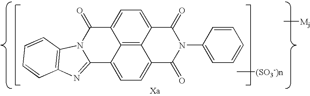


- where n is an integer in the range of 1 to 4 and p is an integer in the range of 0 to 6; Y is individually selected from the group consisting of H, Cl, F, Br, Alk, OH, OAlk, NO2 and NH2; M is a counterion; and j is the number of counterions in the molecule; for n>1, different counterions M can be involved;
-
- sulfoderivatives of heteroaromatic polycycloquinones with the general structural formulas XVIIIa-XVIIId:

- sulfoderivatives of heteroaromatic polycycloquinones with the general structural formulas XVIIIa-XVIIId:
- where A1A2 are fragments of the general structural formula


- X1, X3, X4, X5, X6, X7, X8 are substituents from the group including H, OH, SO3H, such that at least one of these substituents is different from H; Y is a substituent from the series H, Cl, F, Br, Alk, OH, OAlk, NO2, NH2 and p is an integer in the range of 0, 1, 2, 3 and 4; n is one of the group including 0, 1, 2, such that at least one of fragments A1or A2 comprises at least one sulfogroup; M is counterion; and j is the number of counterions in the molecule; for n>1, different counterions M can be involved;
-
- sulfoderivatives of heteroaromatic polycycloquinones with the general structural formulas from the group XIXa-XIXc:

- sulfoderivatives of heteroaromatic polycycloquinones with the general structural formulas from the group XIXa-XIXc:
- where A1A2 are fragments of general structural formula

- X1, X3, X4, X5, X6, X7, X8 are substituents from the group including H, OH, SO3H; Z is a bridge closing new heterocyclic systems chosen from the series —O—, —SO2—, —SO2—O—; Y is a substituent from the series H, Cl, F, Br, Alk, OH, OAlk, NO2, NH2 and p is an integer in the range of 0, 1, 2, 3 and 4; n is one of the group including 0, 1, 2, such that at least one of fragments A1 or A2 comprises at least one sulfogroup; M is counterion; and j is the number of counterions in the molecule; for n>1, different counterions M can be involved;
-
- sulfoderivatives of dyes with anthraquinone fragment with the general structural formulas from the group XX-XXIV:


- sulfoderivatives of dyes with anthraquinone fragment with the general structural formulas from the group XX-XXIV:
- where n is an integer in the range of 1 to 4 and p is an integer in the range of 0 to 8; Y is individually selected from the group consisting of H, Cl, F, Br, Alk, OH, OAlk, NO2 and NH2; M is a counterion; and j is the number of counterions in the molecule; for n>1, different counterions M can be involved;
- sulfoderivatives of fused polycyclic heteroaromatic compounds comprising five or six members with N or O or both (pyrrole, pyridine, oxazole, furan, oxazine, azine, chromone, pyridopyrimidine) with the structural formulas XXV-XXVIII:


- where n is an integer in the range of 1 to 4 and p is an integer in the range of 0 to 8; Y is individually selected from the group consisting of H, Cl, F, Br, Alk, OH, OAlk, NO2 and NH2; M is a counterion; and j is the number of counterions in the molecule; for n>1, different counterions M can be involved.
- A low sensitivity of the disclosed monolithic three-dimensional IC with respect to temperature variations is achieved, in particular, due to the fact that said SCTCFs possess higher temperature stability as compared to the conventional materials. Indeed, SCTCFs can be treated at temperatures of up to 700° C. without any significant change in the electrical properties. The ability of the disclosed three-dimensional ICs to retain their working properties at high ambient temperatures allow these ICs to be used in electronic devices intended for steel making industry (melt level sensors), in aerospace technologies (electronic transducers for engine nozzles), and in many other high-temperature applications.
- Another advantage of SCTCFs implemented in the disclosed monolithic three-dimensional ICs consists in the possibility of using printing technology for the creation of functional semiconductor elements of the discrete ICs.
- Said SCTCFs can be obtained by a method, called Cascade Crystallization Process developed by Optiva Technology. The process is further described in detail in P. Lazarev and M. Paukshto, Proceedings of the 7th International Workshop “Displays, Materials and Components” (Kobe, Japan, Nov. 29-Dec. 1, 2000), pp. 1159-1160. According to this method such an organic compound dissolved in an appropriate solvent forms a colloidal system which is lyotropic liquid crystal solution, in which molecules are aggregated into supramolecules constituting kinetic units of the system. This liquid crystal phase is essentially a precursor of the ordered state of the system, from which a solid anisotropic crystal film is formed in the course of subsequent alignment of the supramolecules and removal of the solvent. The film is also named thin crystal film or TCF.
- A method stipulated for the synthesis of anisotropic semiconducting thin crystal films from a colloidal system with supramolecules includes the following stages:
- (i) application of the aforementioned colloidal system onto a substrate (or onto a device or a layer in a multilayer structure); the colloidal system must possess thixotropic properties, which are provided by maintaining a preset temperature and a certain concentration of the dispersed phase;
- (ii) conversion of the applied colloidal system into a high flow (reduced viscosity) state by any external action (heating, shear straining, etc.) decreasing viscosity of the solution; this action can be either applied during the whole subsequent alignment stage or last for a minimum necessary time, so that the system would not relax into a state with increased viscosity during the alignment stage;
- (iii) external alignment action upon the system, which can be produced using mechanical factors or by any other means; the degree of the external action must be sufficient for the kinetic units of the colloidal system to acquire the necessary orientation and form a structure that would serve as a base of the crystal lattice of the anisotropic thin crystal film;
- (iv) conversion of the aligned region of the layer from the state of reduced viscosity, achieved due to the external action, into the state of the initial or higher viscosity; this transition is performed so as not to cause disorientation of the anisotropic thin crystal film structure and not to produce surface defects;
- (v) final stage of solvent removal (drying), in the course of which the final anisotropic thin crystal film structure is formed; this stage can also include an additional thermal treatment (annealing) characterized by the duration, character, and temperature, which are selected so as to ensure full or at least partial removal of water molecules from said crystal hydrate structure, while retaining the structure of supramolecules and crystalline structure of conjugated aromatic crystalline layer intact.
- In the resulting anisotropic SCTCF, the molecular planes are parallel to each other and the molecules form a three-dimensional crystal structure, at least in a part of the layer. Optimization of the production technology may allow the formation of a single-crystal film.
- The SCTCF thickness usually does not exceed 1 μm. The film thickness can be controlled by changing the content of a solid substance in the applied solution and by varying the applied layer thickness. In order to obtain the films possessing desired optical characteristics, it is possible to use mixed colloidal systems (such mixtures can form joint supramolecules).
- The mixing of said organic compounds in solutions results in the formation of mixed aggregates of variable composition. The analysis of X-ray diffraction patterns for the mixtures allow us to judge about the molecular packing in supramolecules by the presence of a characteristic diffraction peak corresponding to intermolecular spacing in the range from 3.1 to 3.7 Å. In general, this value is common for aromatic compounds in the form of crystals and aggregates. The peak intensity and sharpness increase in the course of drying, however, no changes in the peak position are observed. This diffraction peak corresponds to the intermolecular spacing within aggregates (stacks) and has been observed in the X-ray diffraction patterns of various materials. The mixing is favored by the planar structure of molecules or their fragments and by the coincidence of one molecular dimension in the organic compounds under consideration. In the applied aqueous layer, the organic molecules possess a long-range order in one direction, which is related to the alignment of supramolecules on the substrate surface. As the solvent is evaporated, it is energetically favorable for the molecules to form a three-dimensional crystal structure.
- Thin crystal films obtained by the method described above exhibit electric conductivity of two types: electron, related to the system of π-conjugated bonds in supramolecules, and ionic, related to the ion component of the crystalline film and the presence of free water (solvent). As the water content in the film decreases in the course of drying, the ion component drops; using additional annealing step, this component can be completely eliminated. The electron conductivity component of SCTCFs depends primarily on the length of supramolecules that can be controlled in the course of manufacture. In the presence of an electric field, the free electrons can drift along supramolecules (stacks), while the transitions between stacks are determined by tunneling effects. Thus, SCTCFs possess a pronounced anisotropy of the electrical properties.
- SCTCFs possess a high degree of optical anisotropy as well. Such films exhibit the properties of E-type polarizers, which are related to peculiarities of the optical absorption of supramolecular complexes, and behave as retarders (al known as phase-shifting films) in the spectral ranges where the absorption is insignificant. The retarding properties of these anisotropic films are related to their birefringence (also known as double refraction) that is, to a difference in refractive indices measured in the direction of application of the LLC solution onto a substrate and in the perpendicular direction. Films formed from the LLC systems based on light-fast organic molecules are characterized by high thermal stability and light resistance.
-
FIG. 9 shows the temperature dependence of a SCTCF sample obtained as described above and measured in the direction perpendicular to the direction of application. As can be seen, the resistance decreases with increasing temperature, which is characteristic of semiconductors. The decrease in the resistance reflects an increase in the density of free charge carriers: the higher the sample temperature, the greater the number of mobile free electrons in the conduction band (for a n-type semiconductor) or mobile holes in the valence band (for a p-type semiconductor). - The method illustrated in
FIGS. 5 a -5 d has been demonstrated using a one centimeter square integrated circuit chip with 41-125 μm solder bumps on 250 μm centers along one edge. This chip was mounted perpendicular to a heat sink. Prior to assembly, the first chip was coated with a bonding layer in the form of a rosin-based flux to provide enough tack to hold the chip in position during the reflow process. The assembly was then reflowed in a nitrogen-filled infrared belt furnace. - A thin-film transistor structure with top source and drain contacts was obtained using a silicon wafer with an insulating SiO2 layer. The wafer was coated with SCTCF, above which the electric contacts were deposited by conventional methods.
FIG. 10 shows a schematic diagram of such an organic TFT structure with top source and drain contacts, comprising aSi wafer 55 that serves as a gate contact, a SiO2 insulating layer 56, anSCTCF 57, and gold source anddrain contacts 58. The procedure of depositing contacts consisted of the following steps: (i) cutting a Si/SiO2 wafer covered with SCTCF to the required size; (ii) placing a mask (a mechanical mask was glued to the sample surface using Aquaricum silicone gel); (iii) covering the sample surface with gold. The last stage was performed using an NRC/Varian Model 3117 Thermal Evaporator equipped with a TM-350 thickness monitor (MAXTEC Inc.). The device was operated at a working pressure inside the evaporator of 10−6-10−7 Torr and an evaporator current of 150 A. The typical contact layer thickness was ˜50 nm. All processing steps were visually controlled using a NIKON Eclipse L200 microscope. - The bottom contacts were made using a photolithographic method. The contact pattern was obtained in a
Karl Suss MJB 3 setup. The contacts were deposited in a Temescal VES-2550 electron beam evaporator with an INFICTION IC/5 deposition controller. Covering with Sio2 layer was performed using an Airco Temescal CV-8 electron beam evaporator with an INFICTION XTC/2 deposition controller.FIG. 11 shows a schematic diagram of the TFT structure with bottom source and drain contacts comprising a 500 μmthick Si wafer 61 which also served as the gate contact, a 200 nm thick insulating Sio2 layer 62, anSCTCF 63, a 2.5 nmthick titanium layer 64 for better adhesion of gold, 50 nm thick gold source anddrain contacts 65, and a 800 nm thick protecting SiO2 layer 66. The contacts were deposited perpendicular and parallel to the film coating direction. The samples with different channel lengths and channel widths are available. - The above drawings, examples and specification have illustrated typical preferred embodiments of the disclosed invention and, although specific terms are employed, they are used in a generic and descriptive sense only and not for purposes of limitation, the scope of the invention being set forth in the following claims.
Claims (47)


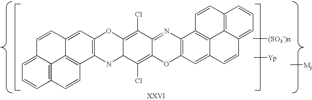


Priority Applications (2)
| Application Number | Priority Date | Filing Date | Title |
|---|---|---|---|
| US10/965,065 US20050104027A1 (en) | 2003-10-17 | 2004-10-13 | Three-dimensional integrated circuit with integrated heat sinks |
| PCT/US2004/034499 WO2005038910A2 (en) | 2003-10-17 | 2004-10-18 | Three-dimensional integrated circuit with integrated heat sinks |
Applications Claiming Priority (2)
| Application Number | Priority Date | Filing Date | Title |
|---|---|---|---|
| US51225603P | 2003-10-17 | 2003-10-17 | |
| US10/965,065 US20050104027A1 (en) | 2003-10-17 | 2004-10-13 | Three-dimensional integrated circuit with integrated heat sinks |
Publications (1)
| Publication Number | Publication Date |
|---|---|
| US20050104027A1 true US20050104027A1 (en) | 2005-05-19 |
Family
ID=34468025
Family Applications (1)
| Application Number | Title | Priority Date | Filing Date |
|---|---|---|---|
| US10/965,065 Abandoned US20050104027A1 (en) | 2003-10-17 | 2004-10-13 | Three-dimensional integrated circuit with integrated heat sinks |
Country Status (2)
| Country | Link |
|---|---|
| US (1) | US20050104027A1 (en) |
| WO (1) | WO2005038910A2 (en) |
Cited By (45)
| Publication number | Priority date | Publication date | Assignee | Title |
|---|---|---|---|---|
| US20060278996A1 (en) * | 2005-06-14 | 2006-12-14 | John Trezza | Active packaging |
| US20060278994A1 (en) * | 2005-06-14 | 2006-12-14 | John Trezza | Inverse chip connector |
| US20060278986A1 (en) * | 2005-06-14 | 2006-12-14 | John Trezza | Chip capacitive coupling |
| US20060281363A1 (en) * | 2005-06-14 | 2006-12-14 | John Trezza | Remote chip attachment |
| US20060278981A1 (en) * | 2005-06-14 | 2006-12-14 | John Trezza | Electronic chip contact structure |
| US20060281303A1 (en) * | 2005-06-14 | 2006-12-14 | John Trezza | Tack & fuse chip bonding |
| US20060281219A1 (en) * | 2005-06-14 | 2006-12-14 | John Trezza | Chip-based thermo-stack |
| US20060278992A1 (en) * | 2005-06-14 | 2006-12-14 | John Trezza | Post & penetration interconnection |
| US20070161235A1 (en) * | 2005-06-14 | 2007-07-12 | John Trezza | Back-to-front via process |
| US20070278641A1 (en) * | 2005-06-14 | 2007-12-06 | John Trezza | Side Stacking Apparatus and Method |
| US20070281460A1 (en) * | 2006-06-06 | 2007-12-06 | Cubic Wafer, Inc. | Front-end processed wafer having through-chip connections |
| US20080090413A1 (en) * | 2006-10-17 | 2008-04-17 | John Trezza | Wafer via formation |
| US20080157787A1 (en) * | 2007-01-03 | 2008-07-03 | Cubic Wafer, Inc. | Sensitivity capacitive sensor |
| US20080197893A1 (en) * | 2007-02-15 | 2008-08-21 | Wyman Theodore J Ted | Variable off-chip drive |
| US20080197488A1 (en) * | 2007-02-15 | 2008-08-21 | John Trezza | Bowed wafer hybridization compensation |
| US20080197508A1 (en) * | 2007-02-16 | 2008-08-21 | John Trezza | Plated pillar package formation |
| US20080200022A1 (en) * | 2007-02-15 | 2008-08-21 | John Callahan | Post-seed deposition process |
| US20080241889A1 (en) * | 2000-12-11 | 2008-10-02 | Invitrogen Corporation | Methods and compositions for synthesis of nucleic acid molecules using multiple recognition sites |
| US20080246145A1 (en) * | 2007-04-05 | 2008-10-09 | John Trezza | Mobile binding in an electronic connection |
| US20080245846A1 (en) * | 2007-04-05 | 2008-10-09 | John Trezza | Heat cycle-able connection |
| US20080261392A1 (en) * | 2007-04-23 | 2008-10-23 | John Trezza | Conductive via formation |
| US20090091892A1 (en) * | 2007-09-26 | 2009-04-09 | Rohm Co., Ltd. | Semiconductor Device |
| US20090267219A1 (en) * | 2007-04-23 | 2009-10-29 | John Trezza | Ultra-thin chip packaging |
| US7687397B2 (en) | 2006-06-06 | 2010-03-30 | John Trezza | Front-end processed wafer having through-chip connections |
| US7763973B1 (en) * | 2007-04-05 | 2010-07-27 | Hewlett-Packard Development Company, L.P. | Integrated heat sink for a microchip |
| US7851348B2 (en) | 2005-06-14 | 2010-12-14 | Abhay Misra | Routingless chip architecture |
| US8304189B2 (en) | 2003-12-01 | 2012-11-06 | Life Technologies Corporation | Nucleic acid molecules containing recombination sites and methods of using the same |
| US8456015B2 (en) | 2005-06-14 | 2013-06-04 | Cufer Asset Ltd. L.L.C. | Triaxial through-chip connection |
| US20140152383A1 (en) * | 2012-11-30 | 2014-06-05 | Dmitri E. Nikonov | Integrated circuits and systems and methods for producing the same |
| US9449896B2 (en) | 2014-01-13 | 2016-09-20 | Stmicroelectronics Sa | Device comprising a three-dimensional integrated structure with simplified thermal dissipation, and corresponding fabrication method |
| WO2019108945A1 (en) * | 2017-12-01 | 2019-06-06 | Silicon Genesis Corporation | Three dimensional integrated circuit |
| US10403435B2 (en) | 2017-12-15 | 2019-09-03 | Capacitor Sciences Incorporated | Edder compound and capacitor thereof |
| US10573627B2 (en) | 2015-01-09 | 2020-02-25 | Silicon Genesis Corporation | Three dimensional integrated circuit |
| US10804252B2 (en) | 2015-01-09 | 2020-10-13 | Silicon Genesis Corporation | Three dimensional integrated circuit |
| US11094576B1 (en) * | 2010-11-18 | 2021-08-17 | Monolithic 3D Inc. | Methods for producing a 3D semiconductor memory device and structure |
| US11164770B1 (en) * | 2010-11-18 | 2021-11-02 | Monolithic 3D Inc. | Method for producing a 3D semiconductor memory device and structure |
| US11217472B2 (en) * | 2010-12-16 | 2022-01-04 | Monolithic 3D Inc. | 3D semiconductor device and structure with multiple isolation layers |
| US11355380B2 (en) * | 2010-11-18 | 2022-06-07 | Monolithic 3D Inc. | Methods for producing 3D semiconductor memory device and structure utilizing alignment marks |
| US11410984B1 (en) | 2021-10-08 | 2022-08-09 | Silicon Genesis Corporation | Three dimensional integrated circuit with lateral connection layer |
| US20220336252A1 (en) * | 2010-11-18 | 2022-10-20 | Monolithic 3D Inc. | Method for producing a 3d semiconductor device and structure with single crystal transistors |
| US11521888B2 (en) * | 2010-11-18 | 2022-12-06 | Monolithic 3D Inc. | 3D semiconductor device and structure with high-k metal gate transistors |
| US11569117B2 (en) * | 2010-11-18 | 2023-01-31 | Monolithic 3D Inc. | 3D semiconductor device and structure with single-crystal layers |
| US20230187256A1 (en) * | 2010-11-18 | 2023-06-15 | Monolithic 3D Inc. | Methods for producing a 3d semiconductor device and structure with memory cells |
| US20230307283A1 (en) * | 2010-11-18 | 2023-09-28 | Monolithic 3D Inc. | Methods for producing a 3d semiconductor device and structure with memory cells and multiple metal layers |
| US11854857B1 (en) * | 2010-11-18 | 2023-12-26 | Monolithic 3D Inc. | Methods for producing a 3D semiconductor device and structure with memory cells and multiple metal layers |
Citations (48)
| Publication number | Priority date | Publication date | Assignee | Title |
|---|---|---|---|---|
| US3438691A (en) * | 1964-05-14 | 1969-04-15 | Polaroid Corp | Birefringent polarizer |
| US3610729A (en) * | 1969-06-18 | 1971-10-05 | Polaroid Corp | Multilayered light polarizer |
| US4525413A (en) * | 1981-03-02 | 1985-06-25 | Polaroid Corporation | Optical device including birefringent polymer |
| US4764846A (en) * | 1987-01-05 | 1988-08-16 | Irvine Sensors Corporation | High density electronic package comprising stacked sub-modules |
| US4894706A (en) * | 1985-02-14 | 1990-01-16 | Nippon Telegraph And Telephone Corporation | Three-dimensional packaging of semiconductor device chips |
| US4896218A (en) * | 1987-09-04 | 1990-01-23 | Rockwell International Corporation | Circularly polarized multi-bandpass interference contrast enhancement filter |
| US4939568A (en) * | 1986-03-20 | 1990-07-03 | Fujitsu Limited | Three-dimensional integrated circuit and manufacturing method thereof |
| US4983533A (en) * | 1987-10-28 | 1991-01-08 | Irvine Sensors Corporation | High-density electronic modules - process and product |
| US5016138A (en) * | 1987-10-27 | 1991-05-14 | Woodman John K | Three dimensional integrated circuit package |
| US5113314A (en) * | 1991-01-24 | 1992-05-12 | Hewlett-Packard Company | High-speed, high-density chip mounting |
| US5126802A (en) * | 1989-02-14 | 1992-06-30 | Ricoh Company, Ltd. | Electric device |
| US5266833A (en) * | 1992-03-30 | 1993-11-30 | Capps David F | Integrated circuit bus structure |
| US5325218A (en) * | 1992-12-31 | 1994-06-28 | Minnesota Mining And Manufacturing Company | Cholesteric polarizer for liquid crystal display and overhead projector |
| US5497033A (en) * | 1993-02-08 | 1996-03-05 | Martin Marietta Corporation | Embedded substrate for integrated circuit modules |
| US5545924A (en) * | 1993-08-05 | 1996-08-13 | Honeywell Inc. | Three dimensional package for monolithic microwave/millimeterwave integrated circuits |
| US5570214A (en) * | 1993-12-15 | 1996-10-29 | Ois Optical Imaging Systems, Inc. | Normally white twisted nematic LCD with retardation films on opposite sides of liquid crystal material for improved viewing zone |
| US5783120A (en) * | 1996-02-29 | 1998-07-21 | Minnesota Mining And Manufacturing Company | Method for making an optical film |
| US5793296A (en) * | 1996-04-30 | 1998-08-11 | Lewkowicz; Mike | Apparatus for carbon monoxide detection and automatic shutoff of a heating system |
| US5793116A (en) * | 1996-05-29 | 1998-08-11 | Mcnc | Microelectronic packaging using arched solder columns |
| US5825543A (en) * | 1996-02-29 | 1998-10-20 | Minnesota Mining And Manufacturing Company | Diffusely reflecting polarizing element including a first birefringent phase and a second phase |
| US5872653A (en) * | 1989-06-20 | 1999-02-16 | Minnesota Mining And Manufacturing Company | Birefringent interference polarizer |
| US5882774A (en) * | 1993-12-21 | 1999-03-16 | Minnesota Mining And Manufacturing Company | Optical film |
| US5943213A (en) * | 1997-11-03 | 1999-08-24 | R-Amtech International, Inc. | Three-dimensional electronic module |
| US5973396A (en) * | 1996-02-16 | 1999-10-26 | Micron Technology, Inc. | Surface mount IC using silicon vias in an area array format or same size as die array |
| US6014313A (en) * | 1996-12-19 | 2000-01-11 | Telefonaktiebolgey Lm Ericsson | Packaging structure for integrated circuits |
| US6025897A (en) * | 1993-12-21 | 2000-02-15 | 3M Innovative Properties Co. | Display with reflective polarizer and randomizing cavity |
| US6174394B1 (en) * | 1993-05-21 | 2001-01-16 | Optiva, Inc. | Method for thermostable and lightfast dichroic light polarizers |
| US20010022497A1 (en) * | 2000-02-23 | 2001-09-20 | Dai Nippon Printing Co., | Electroluminescent device and process for producing the same |
| US6307676B1 (en) * | 1998-01-13 | 2001-10-23 | 3M Innovative Properties Company | Optical device with a dichroic polarizer and a multilayer optical film |
| US20010046086A1 (en) * | 1998-12-23 | 2001-11-29 | 3M Innovative Properties Company | Polymeric interference film |
| US6381137B1 (en) * | 2000-01-27 | 2002-04-30 | Mitsubishi Denki Kabushiki Kaisha | Semiconductor module |
| US6515785B1 (en) * | 1999-04-22 | 2003-02-04 | 3M Innovative Properties Company | Optical devices using reflecting polarizing materials |
| US20030060034A1 (en) * | 1999-04-02 | 2003-03-27 | Imec Vzw, A Research Center In The Country Of Belgium | Method of transferring ultra-thin substrates and application of the method to the manufacture of a multi-layer thin film device |
| US20030071939A1 (en) * | 2001-09-21 | 2003-04-17 | Lazarev Pavel I. | Liquid crystal display with reflecting polarizer |
| US6563640B1 (en) * | 1998-10-28 | 2003-05-13 | Optiva, Inc. | Dichroic polarizer and method for making the same |
| US6569762B2 (en) * | 2000-06-16 | 2003-05-27 | Chartered Semiconductor Manufacturing Ltd. | Three dimensional IC package module |
| US6573565B2 (en) * | 1999-07-28 | 2003-06-03 | International Business Machines Corporation | Method and structure for providing improved thermal conduction for silicon semiconductor devices |
| US20030128518A1 (en) * | 2002-01-07 | 2003-07-10 | International Business Machines Corporation | Common heatsink for multiple chips and modules |
| US6600173B2 (en) * | 2000-08-30 | 2003-07-29 | Cornell Research Foundation, Inc. | Low temperature semiconductor layering and three-dimensional electronic circuits using the layering |
| US6611057B2 (en) * | 2000-11-09 | 2003-08-26 | Nec Corporation | Semiconductor device attaining both high speed processing and sufficient cooling capacity |
| US6627531B2 (en) * | 2000-03-22 | 2003-09-30 | Ziptronix, Inc. | Three dimensional device integration method and integrated device |
| US6633075B1 (en) * | 1999-08-19 | 2003-10-14 | Sharp Kabushiki Kaisha | Heterojunction bipolar transistor and method for fabricating the same |
| US6657607B1 (en) * | 1998-05-29 | 2003-12-02 | Silicon Graphics, Inc. | Liquid crystal flat panel display with enhanced backlight brightness and specially selected light sources |
| US6686654B2 (en) * | 2001-08-31 | 2004-02-03 | Micron Technology, Inc. | Multiple chip stack structure and cooling system |
| US20040215015A1 (en) * | 2003-04-25 | 2004-10-28 | Nazarov Victor V. | Lyotropic liquid crystal systems based on perylenetetracarboxylic acid dibenzimidazole sulfoderivatives, related anisotropic films, and methods for making |
| US6861664B2 (en) * | 2003-07-25 | 2005-03-01 | Xerox Corporation | Device with n-type semiconductor |
| US6947286B2 (en) * | 2003-04-28 | 2005-09-20 | Hewlett-Packard Development Company, L.P. | Stack up assembly |
| US7031162B2 (en) * | 2003-09-26 | 2006-04-18 | International Business Machines Corporation | Method and structure for cooling a dual chip module with one high power chip |
Family Cites Families (3)
| Publication number | Priority date | Publication date | Assignee | Title |
|---|---|---|---|---|
| GB2095039B (en) * | 1981-02-10 | 1984-09-19 | Brown David F | Circuit assembly |
| FR2704690B1 (en) * | 1993-04-27 | 1995-06-23 | Thomson Csf | Method for encapsulating semiconductor wafers, device obtained by this process and application to the interconnection of wafers in three dimensions. |
| US5719745A (en) * | 1995-07-12 | 1998-02-17 | International Business Machines Corporation | Extended surface cooling for chip stack applications |
-
2004
- 2004-10-13 US US10/965,065 patent/US20050104027A1/en not_active Abandoned
- 2004-10-18 WO PCT/US2004/034499 patent/WO2005038910A2/en active Application Filing
Patent Citations (50)
| Publication number | Priority date | Publication date | Assignee | Title |
|---|---|---|---|---|
| US3438691A (en) * | 1964-05-14 | 1969-04-15 | Polaroid Corp | Birefringent polarizer |
| US3610729A (en) * | 1969-06-18 | 1971-10-05 | Polaroid Corp | Multilayered light polarizer |
| US4525413A (en) * | 1981-03-02 | 1985-06-25 | Polaroid Corporation | Optical device including birefringent polymer |
| US4894706A (en) * | 1985-02-14 | 1990-01-16 | Nippon Telegraph And Telephone Corporation | Three-dimensional packaging of semiconductor device chips |
| US4939568A (en) * | 1986-03-20 | 1990-07-03 | Fujitsu Limited | Three-dimensional integrated circuit and manufacturing method thereof |
| US4764846A (en) * | 1987-01-05 | 1988-08-16 | Irvine Sensors Corporation | High density electronic package comprising stacked sub-modules |
| US4896218A (en) * | 1987-09-04 | 1990-01-23 | Rockwell International Corporation | Circularly polarized multi-bandpass interference contrast enhancement filter |
| US5016138A (en) * | 1987-10-27 | 1991-05-14 | Woodman John K | Three dimensional integrated circuit package |
| US4983533A (en) * | 1987-10-28 | 1991-01-08 | Irvine Sensors Corporation | High-density electronic modules - process and product |
| US5126802A (en) * | 1989-02-14 | 1992-06-30 | Ricoh Company, Ltd. | Electric device |
| US6583930B1 (en) * | 1989-06-20 | 2003-06-24 | 3M Innovative Properties | Birefringent interference polarization |
| US5872653A (en) * | 1989-06-20 | 1999-02-16 | Minnesota Mining And Manufacturing Company | Birefringent interference polarizer |
| US5113314A (en) * | 1991-01-24 | 1992-05-12 | Hewlett-Packard Company | High-speed, high-density chip mounting |
| US5266833A (en) * | 1992-03-30 | 1993-11-30 | Capps David F | Integrated circuit bus structure |
| US5325218A (en) * | 1992-12-31 | 1994-06-28 | Minnesota Mining And Manufacturing Company | Cholesteric polarizer for liquid crystal display and overhead projector |
| US5497033A (en) * | 1993-02-08 | 1996-03-05 | Martin Marietta Corporation | Embedded substrate for integrated circuit modules |
| US6174394B1 (en) * | 1993-05-21 | 2001-01-16 | Optiva, Inc. | Method for thermostable and lightfast dichroic light polarizers |
| US5545924A (en) * | 1993-08-05 | 1996-08-13 | Honeywell Inc. | Three dimensional package for monolithic microwave/millimeterwave integrated circuits |
| US5570214A (en) * | 1993-12-15 | 1996-10-29 | Ois Optical Imaging Systems, Inc. | Normally white twisted nematic LCD with retardation films on opposite sides of liquid crystal material for improved viewing zone |
| US6025897A (en) * | 1993-12-21 | 2000-02-15 | 3M Innovative Properties Co. | Display with reflective polarizer and randomizing cavity |
| US5882774A (en) * | 1993-12-21 | 1999-03-16 | Minnesota Mining And Manufacturing Company | Optical film |
| US5973396A (en) * | 1996-02-16 | 1999-10-26 | Micron Technology, Inc. | Surface mount IC using silicon vias in an area array format or same size as die array |
| US5825543A (en) * | 1996-02-29 | 1998-10-20 | Minnesota Mining And Manufacturing Company | Diffusely reflecting polarizing element including a first birefringent phase and a second phase |
| US5783120A (en) * | 1996-02-29 | 1998-07-21 | Minnesota Mining And Manufacturing Company | Method for making an optical film |
| US5793296A (en) * | 1996-04-30 | 1998-08-11 | Lewkowicz; Mike | Apparatus for carbon monoxide detection and automatic shutoff of a heating system |
| US5963793A (en) * | 1996-05-29 | 1999-10-05 | Mcnc | Microelectronic packaging using arched solder columns |
| US5793116A (en) * | 1996-05-29 | 1998-08-11 | Mcnc | Microelectronic packaging using arched solder columns |
| US6014313A (en) * | 1996-12-19 | 2000-01-11 | Telefonaktiebolgey Lm Ericsson | Packaging structure for integrated circuits |
| US5943213A (en) * | 1997-11-03 | 1999-08-24 | R-Amtech International, Inc. | Three-dimensional electronic module |
| US6307676B1 (en) * | 1998-01-13 | 2001-10-23 | 3M Innovative Properties Company | Optical device with a dichroic polarizer and a multilayer optical film |
| US6657607B1 (en) * | 1998-05-29 | 2003-12-02 | Silicon Graphics, Inc. | Liquid crystal flat panel display with enhanced backlight brightness and specially selected light sources |
| US6563640B1 (en) * | 1998-10-28 | 2003-05-13 | Optiva, Inc. | Dichroic polarizer and method for making the same |
| US20010046086A1 (en) * | 1998-12-23 | 2001-11-29 | 3M Innovative Properties Company | Polymeric interference film |
| US20030060034A1 (en) * | 1999-04-02 | 2003-03-27 | Imec Vzw, A Research Center In The Country Of Belgium | Method of transferring ultra-thin substrates and application of the method to the manufacture of a multi-layer thin film device |
| US6515785B1 (en) * | 1999-04-22 | 2003-02-04 | 3M Innovative Properties Company | Optical devices using reflecting polarizing materials |
| US6573565B2 (en) * | 1999-07-28 | 2003-06-03 | International Business Machines Corporation | Method and structure for providing improved thermal conduction for silicon semiconductor devices |
| US6633075B1 (en) * | 1999-08-19 | 2003-10-14 | Sharp Kabushiki Kaisha | Heterojunction bipolar transistor and method for fabricating the same |
| US6381137B1 (en) * | 2000-01-27 | 2002-04-30 | Mitsubishi Denki Kabushiki Kaisha | Semiconductor module |
| US20010022497A1 (en) * | 2000-02-23 | 2001-09-20 | Dai Nippon Printing Co., | Electroluminescent device and process for producing the same |
| US6627531B2 (en) * | 2000-03-22 | 2003-09-30 | Ziptronix, Inc. | Three dimensional device integration method and integrated device |
| US6569762B2 (en) * | 2000-06-16 | 2003-05-27 | Chartered Semiconductor Manufacturing Ltd. | Three dimensional IC package module |
| US6600173B2 (en) * | 2000-08-30 | 2003-07-29 | Cornell Research Foundation, Inc. | Low temperature semiconductor layering and three-dimensional electronic circuits using the layering |
| US6611057B2 (en) * | 2000-11-09 | 2003-08-26 | Nec Corporation | Semiconductor device attaining both high speed processing and sufficient cooling capacity |
| US6686654B2 (en) * | 2001-08-31 | 2004-02-03 | Micron Technology, Inc. | Multiple chip stack structure and cooling system |
| US20030071939A1 (en) * | 2001-09-21 | 2003-04-17 | Lazarev Pavel I. | Liquid crystal display with reflecting polarizer |
| US20030128518A1 (en) * | 2002-01-07 | 2003-07-10 | International Business Machines Corporation | Common heatsink for multiple chips and modules |
| US20040215015A1 (en) * | 2003-04-25 | 2004-10-28 | Nazarov Victor V. | Lyotropic liquid crystal systems based on perylenetetracarboxylic acid dibenzimidazole sulfoderivatives, related anisotropic films, and methods for making |
| US6947286B2 (en) * | 2003-04-28 | 2005-09-20 | Hewlett-Packard Development Company, L.P. | Stack up assembly |
| US6861664B2 (en) * | 2003-07-25 | 2005-03-01 | Xerox Corporation | Device with n-type semiconductor |
| US7031162B2 (en) * | 2003-09-26 | 2006-04-18 | International Business Machines Corporation | Method and structure for cooling a dual chip module with one high power chip |
Cited By (115)
| Publication number | Priority date | Publication date | Assignee | Title |
|---|---|---|---|---|
| US9309520B2 (en) | 2000-08-21 | 2016-04-12 | Life Technologies Corporation | Methods and compositions for synthesis of nucleic acid molecules using multiple recognition sites |
| US8030066B2 (en) | 2000-12-11 | 2011-10-04 | Life Technologies Corporation | Methods and compositions for synthesis of nucleic acid molecules using multiple recognition sites |
| US20080241889A1 (en) * | 2000-12-11 | 2008-10-02 | Invitrogen Corporation | Methods and compositions for synthesis of nucleic acid molecules using multiple recognition sites |
| US8945884B2 (en) | 2000-12-11 | 2015-02-03 | Life Technologies Corporation | Methods and compositions for synthesis of nucleic acid molecules using multiplerecognition sites |
| US9534252B2 (en) | 2003-12-01 | 2017-01-03 | Life Technologies Corporation | Nucleic acid molecules containing recombination sites and methods of using the same |
| US8304189B2 (en) | 2003-12-01 | 2012-11-06 | Life Technologies Corporation | Nucleic acid molecules containing recombination sites and methods of using the same |
| US8456015B2 (en) | 2005-06-14 | 2013-06-04 | Cufer Asset Ltd. L.L.C. | Triaxial through-chip connection |
| US20060281219A1 (en) * | 2005-06-14 | 2006-12-14 | John Trezza | Chip-based thermo-stack |
| US20090137116A1 (en) * | 2005-06-14 | 2009-05-28 | Cufer Asset Ltd. L.L.C. | Isolating chip-to-chip contact |
| US20060281303A1 (en) * | 2005-06-14 | 2006-12-14 | John Trezza | Tack & fuse chip bonding |
| US8232194B2 (en) | 2005-06-14 | 2012-07-31 | Cufer Asset Ltd. L.L.C. | Process for chip capacitive coupling |
| US20060278992A1 (en) * | 2005-06-14 | 2006-12-14 | John Trezza | Post & penetration interconnection |
| WO2006138489A2 (en) * | 2005-06-14 | 2006-12-28 | Cubic Wafer, Inc. | Chip-based thermo-stack |
| US20070138562A1 (en) * | 2005-06-14 | 2007-06-21 | Cubic Wafer, Inc. | Coaxial through chip connection |
| US20070161235A1 (en) * | 2005-06-14 | 2007-07-12 | John Trezza | Back-to-front via process |
| US20070167004A1 (en) * | 2005-06-14 | 2007-07-19 | John Trezza | Triaxial through-chip connection |
| US20070182020A1 (en) * | 2005-06-14 | 2007-08-09 | John Trezza | Chip connector |
| US20070196948A1 (en) * | 2005-06-14 | 2007-08-23 | John Trezza | Stacked chip-based system and method |
| US20070197013A1 (en) * | 2005-06-14 | 2007-08-23 | Cubic Wafer, Inc. | Processed Wafer Via |
| US20070228576A1 (en) * | 2005-06-14 | 2007-10-04 | John Trezza | Isolating chip-to-chip contact |
| WO2006138489A3 (en) * | 2005-06-14 | 2007-11-15 | Cubic Wafer Inc | Chip-based thermo-stack |
| US20070278641A1 (en) * | 2005-06-14 | 2007-12-06 | John Trezza | Side Stacking Apparatus and Method |
| US7989958B2 (en) | 2005-06-14 | 2011-08-02 | Cufer Assett Ltd. L.L.C. | Patterned contact |
| US20060278981A1 (en) * | 2005-06-14 | 2006-12-14 | John Trezza | Electronic chip contact structure |
| US9324629B2 (en) | 2005-06-14 | 2016-04-26 | Cufer Asset Ltd. L.L.C. | Tooling for coupling multiple electronic chips |
| US20060281307A1 (en) * | 2005-06-14 | 2006-12-14 | John Trezza | Post-attachment chip-to-chip connection |
| US9147635B2 (en) | 2005-06-14 | 2015-09-29 | Cufer Asset Ltd. L.L.C. | Contact-based encapsulation |
| US20060278966A1 (en) * | 2005-06-14 | 2006-12-14 | John Trezza | Contact-based encapsulation |
| US8846445B2 (en) | 2005-06-14 | 2014-09-30 | Cufer Asset Ltd. L.L.C. | Inverse chip connector |
| US20060281363A1 (en) * | 2005-06-14 | 2006-12-14 | John Trezza | Remote chip attachment |
| US8197627B2 (en) | 2005-06-14 | 2012-06-12 | Cufer Asset Ltd. L.L.C. | Pin-type chip tooling |
| US7969015B2 (en) | 2005-06-14 | 2011-06-28 | Cufer Asset Ltd. L.L.C. | Inverse chip connector |
| US20060278986A1 (en) * | 2005-06-14 | 2006-12-14 | John Trezza | Chip capacitive coupling |
| US8283778B2 (en) | 2005-06-14 | 2012-10-09 | Cufer Asset Ltd. L.L.C. | Thermally balanced via |
| US20060278993A1 (en) * | 2005-06-14 | 2006-12-14 | John Trezza | Chip connector |
| US20060281243A1 (en) * | 2005-06-14 | 2006-12-14 | John Trezza | Through chip connection |
| US8643186B2 (en) | 2005-06-14 | 2014-02-04 | Cufer Asset Ltd. L.L.C. | Processed wafer via |
| US7659202B2 (en) | 2005-06-14 | 2010-02-09 | John Trezza | Triaxial through-chip connection |
| US8197626B2 (en) | 2005-06-14 | 2012-06-12 | Cufer Asset Ltd. L.L.C. | Rigid-backed, membrane-based chip tooling |
| US8154131B2 (en) | 2005-06-14 | 2012-04-10 | Cufer Asset Ltd. L.L.C. | Profiled contact |
| US7687400B2 (en) | 2005-06-14 | 2010-03-30 | John Trezza | Side stacking apparatus and method |
| US7946331B2 (en) | 2005-06-14 | 2011-05-24 | Cufer Asset Ltd. L.L.C. | Pin-type chip tooling |
| US8093729B2 (en) | 2005-06-14 | 2012-01-10 | Cufer Asset Ltd. L.L.C. | Electrically conductive interconnect system and method |
| US8084851B2 (en) | 2005-06-14 | 2011-12-27 | Cufer Asset Ltd. L.L.C. | Side stacking apparatus and method |
| US8067312B2 (en) | 2005-06-14 | 2011-11-29 | Cufer Asset Ltd. L.L.C. | Coaxial through chip connection |
| US8053903B2 (en) | 2005-06-14 | 2011-11-08 | Cufer Asset Ltd. L.L.C. | Chip capacitive coupling |
| US7767493B2 (en) | 2005-06-14 | 2010-08-03 | John Trezza | Post & penetration interconnection |
| US7781886B2 (en) | 2005-06-14 | 2010-08-24 | John Trezza | Electronic chip contact structure |
| US7785987B2 (en) | 2005-06-14 | 2010-08-31 | John Trezza | Isolating chip-to-chip contact |
| US7785931B2 (en) | 2005-06-14 | 2010-08-31 | John Trezza | Chip-based thermo-stack |
| US7786592B2 (en) | 2005-06-14 | 2010-08-31 | John Trezza | Chip capacitive coupling |
| US20060278994A1 (en) * | 2005-06-14 | 2006-12-14 | John Trezza | Inverse chip connector |
| US7808111B2 (en) | 2005-06-14 | 2010-10-05 | John Trezza | Processed wafer via |
| US7838997B2 (en) | 2005-06-14 | 2010-11-23 | John Trezza | Remote chip attachment |
| US7847412B2 (en) | 2005-06-14 | 2010-12-07 | John Trezza | Isolating chip-to-chip contact |
| US7851348B2 (en) | 2005-06-14 | 2010-12-14 | Abhay Misra | Routingless chip architecture |
| US8021922B2 (en) | 2005-06-14 | 2011-09-20 | Cufer Asset Ltd. L.L.C. | Remote chip attachment |
| US20060278996A1 (en) * | 2005-06-14 | 2006-12-14 | John Trezza | Active packaging |
| US7884483B2 (en) | 2005-06-14 | 2011-02-08 | Cufer Asset Ltd. L.L.C. | Chip connector |
| US7919870B2 (en) | 2005-06-14 | 2011-04-05 | Cufer Asset Ltd. L.L.C. | Coaxial through chip connection |
| US7932584B2 (en) | 2005-06-14 | 2011-04-26 | Cufer Asset Ltd. L.L.C. | Stacked chip-based system and method |
| US7942182B2 (en) | 2005-06-14 | 2011-05-17 | Cufer Asset Ltd. L.L.C. | Rigid-backed, membrane-based chip tooling |
| US7687397B2 (en) | 2006-06-06 | 2010-03-30 | John Trezza | Front-end processed wafer having through-chip connections |
| US20070281460A1 (en) * | 2006-06-06 | 2007-12-06 | Cubic Wafer, Inc. | Front-end processed wafer having through-chip connections |
| US7871927B2 (en) | 2006-10-17 | 2011-01-18 | Cufer Asset Ltd. L.L.C. | Wafer via formation |
| US20080090413A1 (en) * | 2006-10-17 | 2008-04-17 | John Trezza | Wafer via formation |
| US7705613B2 (en) | 2007-01-03 | 2010-04-27 | Abhay Misra | Sensitivity capacitive sensor |
| US8499434B2 (en) | 2007-01-03 | 2013-08-06 | Cufer Asset Ltd. L.L.C. | Method of making a capacitive sensor |
| US20080157787A1 (en) * | 2007-01-03 | 2008-07-03 | Cubic Wafer, Inc. | Sensitivity capacitive sensor |
| US20100055838A1 (en) * | 2007-01-03 | 2010-03-04 | Abhay Misra | Sensitivity capacitive sensor |
| US20080197893A1 (en) * | 2007-02-15 | 2008-08-21 | Wyman Theodore J Ted | Variable off-chip drive |
| US7969192B2 (en) | 2007-02-15 | 2011-06-28 | Cufer Asset Ltd. L.L.C. | Variable off-chip drive |
| US20100176844A1 (en) * | 2007-02-15 | 2010-07-15 | Wyman Theodore J Ted | Variable off-chip drive |
| US20080200022A1 (en) * | 2007-02-15 | 2008-08-21 | John Callahan | Post-seed deposition process |
| US20080197488A1 (en) * | 2007-02-15 | 2008-08-21 | John Trezza | Bowed wafer hybridization compensation |
| US7803693B2 (en) | 2007-02-15 | 2010-09-28 | John Trezza | Bowed wafer hybridization compensation |
| US7598163B2 (en) | 2007-02-15 | 2009-10-06 | John Callahan | Post-seed deposition process |
| US20080197508A1 (en) * | 2007-02-16 | 2008-08-21 | John Trezza | Plated pillar package formation |
| US7670874B2 (en) | 2007-02-16 | 2010-03-02 | John Trezza | Plated pillar package formation |
| US7748116B2 (en) | 2007-04-05 | 2010-07-06 | John Trezza | Mobile binding in an electronic connection |
| US20080245846A1 (en) * | 2007-04-05 | 2008-10-09 | John Trezza | Heat cycle-able connection |
| US7850060B2 (en) | 2007-04-05 | 2010-12-14 | John Trezza | Heat cycle-able connection |
| US20080246145A1 (en) * | 2007-04-05 | 2008-10-09 | John Trezza | Mobile binding in an electronic connection |
| US7763973B1 (en) * | 2007-04-05 | 2010-07-27 | Hewlett-Packard Development Company, L.P. | Integrated heat sink for a microchip |
| US20080261392A1 (en) * | 2007-04-23 | 2008-10-23 | John Trezza | Conductive via formation |
| US7960210B2 (en) | 2007-04-23 | 2011-06-14 | Cufer Asset Ltd. L.L.C. | Ultra-thin chip packaging |
| US20090267219A1 (en) * | 2007-04-23 | 2009-10-29 | John Trezza | Ultra-thin chip packaging |
| US20090091892A1 (en) * | 2007-09-26 | 2009-04-09 | Rohm Co., Ltd. | Semiconductor Device |
| US11164770B1 (en) * | 2010-11-18 | 2021-11-02 | Monolithic 3D Inc. | Method for producing a 3D semiconductor memory device and structure |
| US11804396B2 (en) * | 2010-11-18 | 2023-10-31 | Monolithic 3D Inc. | Methods for producing a 3D semiconductor device and structure with memory cells and multiple metal layers |
| US11610802B2 (en) * | 2010-11-18 | 2023-03-21 | Monolithic 3D Inc. | Method for producing a 3D semiconductor device and structure with single crystal transistors and metal gate electrodes |
| US11569117B2 (en) * | 2010-11-18 | 2023-01-31 | Monolithic 3D Inc. | 3D semiconductor device and structure with single-crystal layers |
| US11521888B2 (en) * | 2010-11-18 | 2022-12-06 | Monolithic 3D Inc. | 3D semiconductor device and structure with high-k metal gate transistors |
| US11862503B2 (en) * | 2010-11-18 | 2024-01-02 | Monolithic 3D Inc. | Method for producing a 3D semiconductor device and structure with memory cells and multiple metal layers |
| US20230420283A1 (en) * | 2010-11-18 | 2023-12-28 | Monolithic 3D Inc. | Methods for producing a 3d semiconductor device and structure with memory cells and multiple metal layers |
| US20220336252A1 (en) * | 2010-11-18 | 2022-10-20 | Monolithic 3D Inc. | Method for producing a 3d semiconductor device and structure with single crystal transistors |
| US11854857B1 (en) * | 2010-11-18 | 2023-12-26 | Monolithic 3D Inc. | Methods for producing a 3D semiconductor device and structure with memory cells and multiple metal layers |
| US20230187256A1 (en) * | 2010-11-18 | 2023-06-15 | Monolithic 3D Inc. | Methods for producing a 3d semiconductor device and structure with memory cells |
| US11094576B1 (en) * | 2010-11-18 | 2021-08-17 | Monolithic 3D Inc. | Methods for producing a 3D semiconductor memory device and structure |
| US20230307283A1 (en) * | 2010-11-18 | 2023-09-28 | Monolithic 3D Inc. | Methods for producing a 3d semiconductor device and structure with memory cells and multiple metal layers |
| US11355380B2 (en) * | 2010-11-18 | 2022-06-07 | Monolithic 3D Inc. | Methods for producing 3D semiconductor memory device and structure utilizing alignment marks |
| US11217472B2 (en) * | 2010-12-16 | 2022-01-04 | Monolithic 3D Inc. | 3D semiconductor device and structure with multiple isolation layers |
| US8963135B2 (en) * | 2012-11-30 | 2015-02-24 | Intel Corporation | Integrated circuits and systems and methods for producing the same |
| US20140152383A1 (en) * | 2012-11-30 | 2014-06-05 | Dmitri E. Nikonov | Integrated circuits and systems and methods for producing the same |
| CN104756255A (en) * | 2012-11-30 | 2015-07-01 | 英特尔公司 | Integrated circuits and systems and methods for producing the same |
| TWI552309B (en) * | 2012-11-30 | 2016-10-01 | 英特爾股份有限公司 | Integrated circuits and systems and methods for producing the same |
| US9449896B2 (en) | 2014-01-13 | 2016-09-20 | Stmicroelectronics Sa | Device comprising a three-dimensional integrated structure with simplified thermal dissipation, and corresponding fabrication method |
| US10573627B2 (en) | 2015-01-09 | 2020-02-25 | Silicon Genesis Corporation | Three dimensional integrated circuit |
| US11626392B2 (en) | 2015-01-09 | 2023-04-11 | Silicon Genesis Corporation | Method of forming semiconductor device using range compensating material |
| US10923459B2 (en) | 2015-01-09 | 2021-02-16 | Silicon Genesis Corporation | Three dimensional integrated circuit |
| US10804252B2 (en) | 2015-01-09 | 2020-10-13 | Silicon Genesis Corporation | Three dimensional integrated circuit |
| WO2019108945A1 (en) * | 2017-12-01 | 2019-06-06 | Silicon Genesis Corporation | Three dimensional integrated circuit |
| US10403435B2 (en) | 2017-12-15 | 2019-09-03 | Capacitor Sciences Incorporated | Edder compound and capacitor thereof |
| US11410984B1 (en) | 2021-10-08 | 2022-08-09 | Silicon Genesis Corporation | Three dimensional integrated circuit with lateral connection layer |
| US11901351B2 (en) | 2021-10-08 | 2024-02-13 | Silicon Genesis Corporation | Three dimensional integrated circuit with lateral connection layer |
Also Published As
| Publication number | Publication date |
|---|---|
| WO2005038910A2 (en) | 2005-04-28 |
| WO2005038910A3 (en) | 2005-08-11 |
Similar Documents
| Publication | Publication Date | Title |
|---|---|---|
| US20050104027A1 (en) | Three-dimensional integrated circuit with integrated heat sinks | |
| JP2589918B2 (en) | Microelectronic circuit package rework method | |
| US7880285B2 (en) | Semiconductor device comprising a semiconductor chip stack and method for producing the same | |
| US8669175B2 (en) | Semiconductor device and manufacturing of the semiconductor device | |
| US7352063B2 (en) | Semiconductor structure that includes a cooling structure formed on a semiconductor surface and method of manufacturing the same | |
| TW202329351A (en) | Thermal bypass for stacked dies | |
| CN110060935A (en) | Semiconductor devices and its manufacturing method | |
| US20240096816A1 (en) | Semiconductor device and method of manufacture | |
| US20090032933A1 (en) | Redistributed chip packaging with thermal contact to device backside | |
| US7049695B1 (en) | Method and device for heat dissipation in semiconductor modules | |
| CN107068645A (en) | Semiconductor devices and manufacture method | |
| TWI238483B (en) | Semiconductor electrical connecting structure and method for fabricating the same | |
| US7095111B2 (en) | Package with integrated wick layer and method for heat removal | |
| KR102238309B1 (en) | Semiconductor device and method of manufacture | |
| TWI574333B (en) | Electronic package and method for fabricating the same | |
| TWI636535B (en) | Glass interposer with embedded thermoelectric devices | |
| CN114999943B (en) | Interconnection method of microstructure array and device bonding structure | |
| TWI574365B (en) | Integrated circuit structures and methods for forming the same | |
| US10727192B2 (en) | Multiple sized bump bonds | |
| RU2299497C2 (en) | Method for producing three-dimensional multichip micromodule | |
| US5946597A (en) | Semiconductor chip mounting method | |
| TWI459512B (en) | Vertically packaged mosfet and ic power devices as integrated module using 3d interconnected laminates | |
| KR20090031289A (en) | Flip chip structure and method of manufacture | |
| Yin et al. | High temperature embedded power module | |
| US11837521B2 (en) | Wire bonded air heat sink |
Legal Events
| Date | Code | Title | Description |
|---|---|---|---|
| AS | Assignment |
Owner name: OPTIVA, INC., CALIFORNIA Free format text: ASSIGNMENT OF ASSIGNORS INTEREST;ASSIGNOR:LAZAREV, PAVEL I.;REEL/FRAME:015906/0907 Effective date: 20041006 |
|
| AS | Assignment |
Owner name: NITTO DENKO CORPORATION,JAPAN Free format text: ASSIGNMENT OF ASSIGNORS INTEREST;ASSIGNOR:INSOLVENCY SERVICES GROUP, INC.;REEL/FRAME:016835/0383 Effective date: 20050519 Owner name: NITTO DENKO CORPORATION, JAPAN Free format text: ASSIGNMENT OF ASSIGNORS INTEREST;ASSIGNOR:INSOLVENCY SERVICES GROUP, INC.;REEL/FRAME:016835/0383 Effective date: 20050519 |
|
| AS | Assignment |
Owner name: INSOLVENCY SERVICES GROUP, INC.,CALIFORNIA Free format text: ASSIGNMENT OF ASSIGNORS INTEREST;ASSIGNOR:OPTIVA, INC.;REEL/FRAME:016891/0382 Effective date: 20050519 Owner name: INSOLVENCY SERVICES GROUP, INC., CALIFORNIA Free format text: ASSIGNMENT OF ASSIGNORS INTEREST;ASSIGNOR:OPTIVA, INC.;REEL/FRAME:016891/0382 Effective date: 20050519 |
|
| STCB | Information on status: application discontinuation |
Free format text: ABANDONED -- FAILURE TO RESPOND TO AN OFFICE ACTION |