US20040253547A1 - Pattern formation method - Google Patents
Pattern formation method Download PDFInfo
- Publication number
- US20040253547A1 US20040253547A1 US10/661,540 US66154003A US2004253547A1 US 20040253547 A1 US20040253547 A1 US 20040253547A1 US 66154003 A US66154003 A US 66154003A US 2004253547 A1 US2004253547 A1 US 2004253547A1
- Authority
- US
- United States
- Prior art keywords
- resist film
- formation method
- pattern
- acid
- pattern formation
- Prior art date
- Legal status (The legal status is an assumption and is not a legal conclusion. Google has not performed a legal analysis and makes no representation as to the accuracy of the status listed.)
- Abandoned
Links
Images


Classifications
-
- G—PHYSICS
- G03—PHOTOGRAPHY; CINEMATOGRAPHY; ANALOGOUS TECHNIQUES USING WAVES OTHER THAN OPTICAL WAVES; ELECTROGRAPHY; HOLOGRAPHY
- G03F—PHOTOMECHANICAL PRODUCTION OF TEXTURED OR PATTERNED SURFACES, e.g. FOR PRINTING, FOR PROCESSING OF SEMICONDUCTOR DEVICES; MATERIALS THEREFOR; ORIGINALS THEREFOR; APPARATUS SPECIALLY ADAPTED THEREFOR
- G03F7/00—Photomechanical, e.g. photolithographic, production of textured or patterned surfaces, e.g. printing surfaces; Materials therefor, e.g. comprising photoresists; Apparatus specially adapted therefor
- G03F7/20—Exposure; Apparatus therefor
- G03F7/2041—Exposure; Apparatus therefor in the presence of a fluid, e.g. immersion; using fluid cooling means
-
- G—PHYSICS
- G03—PHOTOGRAPHY; CINEMATOGRAPHY; ANALOGOUS TECHNIQUES USING WAVES OTHER THAN OPTICAL WAVES; ELECTROGRAPHY; HOLOGRAPHY
- G03F—PHOTOMECHANICAL PRODUCTION OF TEXTURED OR PATTERNED SURFACES, e.g. FOR PRINTING, FOR PROCESSING OF SEMICONDUCTOR DEVICES; MATERIALS THEREFOR; ORIGINALS THEREFOR; APPARATUS SPECIALLY ADAPTED THEREFOR
- G03F7/00—Photomechanical, e.g. photolithographic, production of textured or patterned surfaces, e.g. printing surfaces; Materials therefor, e.g. comprising photoresists; Apparatus specially adapted therefor
- G03F7/004—Photosensitive materials
- G03F7/038—Macromolecular compounds which are rendered insoluble or differentially wettable
- G03F7/0382—Macromolecular compounds which are rendered insoluble or differentially wettable the macromolecular compound being present in a chemically amplified negative photoresist composition
-
- G—PHYSICS
- G03—PHOTOGRAPHY; CINEMATOGRAPHY; ANALOGOUS TECHNIQUES USING WAVES OTHER THAN OPTICAL WAVES; ELECTROGRAPHY; HOLOGRAPHY
- G03F—PHOTOMECHANICAL PRODUCTION OF TEXTURED OR PATTERNED SURFACES, e.g. FOR PRINTING, FOR PROCESSING OF SEMICONDUCTOR DEVICES; MATERIALS THEREFOR; ORIGINALS THEREFOR; APPARATUS SPECIALLY ADAPTED THEREFOR
- G03F7/00—Photomechanical, e.g. photolithographic, production of textured or patterned surfaces, e.g. printing surfaces; Materials therefor, e.g. comprising photoresists; Apparatus specially adapted therefor
- G03F7/004—Photosensitive materials
- G03F7/039—Macromolecular compounds which are photodegradable, e.g. positive electron resists
- G03F7/0392—Macromolecular compounds which are photodegradable, e.g. positive electron resists the macromolecular compound being present in a chemically amplified positive photoresist composition
- G03F7/0395—Macromolecular compounds which are photodegradable, e.g. positive electron resists the macromolecular compound being present in a chemically amplified positive photoresist composition the macromolecular compound having a backbone with alicyclic moieties
Definitions
- the present invention relates to a pattern formation method for use in fabrication process and the like for semiconductor devices.
- the aforementioned chemically amplified resist material is applied on a substrate 1 so as to form a resist film 2 with a thickness of 0.20 ⁇ m.
- an exposed portion 2 a of the resist film 2 becomes soluble in an alkaline developer because an acid is generated from the acid generator therein while an unexposed portion 2 b of the resist film 2 remains insoluble in an alkaline developer because no acid is generated from the acid generator therein.
- the resist film 2 is baked with a hot plate at a temperature of 100° C. for 60 seconds, and the resultant resist film is developed with a 2.38 wt % tetramethylammonium hydroxide developer (alkaline developer). In this manner, a resist pattern 6 made of the unexposed portion 2 b of the resist film 2 can be obtained as shown in FIG. 9D.
- the resist pattern 6 formed by the conventional pattern formation method is in a defective T-top shape.
- the resist pattern 6 is in the T-top shape.
- the resultant resist pattern is in a defective shape with round shoulders.
- an object of the invention is forming a resist pattern in a good shape by the immersion lithography.
- the present inventors have examined the cause of the defective shape of the conventional resist pattern formed by the immersion lithography, resulting in finding the following: Since the pattern exposure is carried out while supplying, onto the resist film, a water-repellent nonaqueous solution of, for example, perfluoropolyether, the water-repellent nonaqueous solution remains on the resist film in the development performed after the pattern exposure. This remaining nonaqueous solution inhibits the developer from permeating into the resist film. Also, it has been found that when water is present on a resist film after the pattern exposure, a developer can easily permeate into the resist film owing to the affinity of the water.
- the present invention was devised on the basis of these findings and is specifically practiced as follows:
- the first pattern formation method of this invention includes the steps of forming a resist film; performing pattern exposure by selectively irradiating the resist film with exposing light while supplying, onto the resist film, a nonaqueous solution including water; and forming a resist pattern by developing the resist film after the pattern exposure.
- the nonaqueous solution includes water
- the surface of the resist film attains affinity owing to the water after the pattern exposure, so that a developer can easily permeate into the resist film. Accordingly, the resist pattern can be formed in a good shape, and hence, a pattern of a target film etched by using the resist pattern can be also in a good shape.
- the second pattern formation method of this invention includes the steps of forming a positive resist film of a chemically amplified resist material including an acid generator for generating an acid through irradiation with light; performing pattern exposure by selectively irradiating the resist film with exposing light while supplying, onto the resist film, a nonaqueous solution including a compound for generating water in the presence of an acid; and forming a resist pattern by developing the resist film after the pattern exposure.
- the resist film includes the acid generator and the nonaqueous solution includes the compound for generating water in the presence of an acid
- the surface of an exposed portion of the resist film attains affinity owing to generated water after the pattern exposure, so that a developer can easily permeate into the exposed portion of the resist film. Accordingly, the resist pattern can be formed in a good shape, and hence, a pattern of a target film etched by using the resist pattern can be also in a good shape.
- the third pattern formation method of this invention includes the steps of forming a positive resist film; performing pattern exposure by selectively irradiating the resist film with exposing light while supplying, onto the resist film, a nonaqueous solution including an acid generator for generating an acid through irradiation with light and a compound for generating water in the presence of an acid; and forming a resist pattern by developing the resist film after the pattern exposure.
- the nonaqueous solution includes the acid generator and the compound for generating water in the presence of an acid
- the surface of an exposed portion of the resist film attains affinity owing to generated water after the pattern exposure, so that a developer can easily permeate into the exposed portion of the resist film. Accordingly, the resist pattern can be formed in a good shape, and hence, a pattern of a target film etched by using the resist pattern can be also in a good shape.
- the fourth pattern formation method of this invention includes the steps of forming a positive resist film of a chemically amplified resist material including an acid generator for generating an acid through irradiation with light; forming, on the resist film, a water-soluble film including a compound for generating water in the presence of an acid; performing pattern exposure by selectively irradiating the resist film with exposing light while supplying a nonaqueous solution onto the water-soluble film; and forming a resist pattern by developing the resist film after the pattern exposure.
- the resist film includes the acid generator and the water-soluble film formed on the resist film includes the compound for generating water in the presence of an acid, the surfaces of the water-soluble film and an exposed portion of the resist film attain affinity owing to generated water after the pattern exposure, so that a developer can easily permeate into the exposed portion of the resist film. Accordingly, the resist pattern can be formed in a good shape, and hence, a pattern of a target film etched by using the resist pattern can be also in a good shape.
- the fifth pattern formation method of this invention includes the steps of forming a positive resist film; forming, on the resist film, a water-soluble film including an acid generator for generating an acid through irradiation with light and a compound for generating water in the presence of an acid; performing pattern exposure by selectively irradiating the resist film with exposing light while supplying a nonaqueous solution onto the water-soluble film; and forming a resist pattern by developing the resist film after the pattern exposure.
- the water-soluble film formed on the resist film includes the acid generator and the compound for generating water in the presence of an acid
- the surfaces of the water-soluble film and an exposed portion of the resist film attain affinity owing to generated water after the pattern exposure, so that a developer can easily permeate into the exposed portion of the resist film. Accordingly, the resist pattern can be formed in a good shape, and hence, a pattern of a target film etched by using the resist pattern can be also in a good shape.
- the sixth pattern formation method of this invention includes the steps of forming a positive resist film of a chemically amplified resist material including an acid generator for generating an acid through irradiation with light and a compound for generating water in the presence of an acid; performing pattern exposure by selectively irradiating the resist film with exposing light while supplying a nonaqueous solution onto the resist film; and forming a resist pattern by developing the resist film after the pattern exposure.
- the resist film since the resist film includes the acid generator and the compound for generating water in the presence of an acid, the surface of an exposed portion of the resist film attains affinity owing to generated water after the pattern exposure, so that a developer can easily permeate into the exposed portion of the resist film. Accordingly, the resist pattern can be formed in a good shape, and hence, a pattern of a target film etched by using the resist pattern can be also in a good shape.
- the nonaqueous solution can be perfluoropolyether.
- the exposing light is preferably F 2 laser.
- the nonaqueous solution preferably includes water.
- the affinity of the exposed portion of the resist film can be further improved, and hence, the developer can more easily permeate into the exposed portion of the resist film.
- the nonaqueous solution preferably includes a compound for generating water in the presence of an acid.
- the affinity of the exposed portion of the resist film can be further improved, and hence, the developer can more easily permeate into the exposed portion of the resist film.
- the chemically amplified resist material preferably includes a compound for generating water in the presence of an acid.
- the affinity of the exposed portion of the resist film can be further improved, and hence, the developer can more easily permeate into the exposed portion of the resist film.
- the acid generator can be an onium salt, a halogen-containing compound, a diazoketone compound, a diazomethane compound, a sulfone compound, a sulfonic ester compound or a sulfonimide compound.
- the compound for generating water in the presence of an acid can be a tertiary alcohol, a diol of a tertiary alcohol, a secondary alcohol or a diol of a secondary alcohol.
- the water-soluble film can be a polyvinyl alcohol film or a polyvinyl pyrrolidone film.
- FIG. 1 is a partial cross-sectional view of an exposure system commonly used in preferred embodiments of the invention.
- FIGS. 2A, 2B, 2 C and 2 D are cross-sectional views for showing procedures in a pattern formation method according to Embodiment 1 of the invention.
- FIGS. 3A, 3B, 3 C and 3 D are cross-sectional views for showing procedures in a pattern formation method according to Embodiment 2 of the invention.
- FIGS. 4A, 4B, 4 C and 4 D are cross-sectional views for showing procedures in a pattern formation method according to Embodiment 3 of the invention.
- FIGS. 5A, 5B, 5 C and 5 D are cross-sectional views for showing procedures in a pattern formation method according to Embodiment 4 of the invention.
- FIGS. 6A, 6B, 6 C and 6 D are cross-sectional views for showing procedures in a pattern formation method according to Embodiment 5 of the invention.
- FIGS. 7A, 7B, 7 C and 7 D are cross-sectional views for showing procedures in a pattern formation method according to Embodiment 6 of the invention.
- FIGS. 8A, 8B, 8 C and 8 D are cross-sectional views for showing procedures in a pattern formation method according to Embodiment 7 of the invention.
- FIGS. 9A, 9B, 9 C and 9 D are cross-sectional views for showing procedures in a conventional pattern formation method.
- Pattern formation methods according to preferred embodiments of the invention will now be described, and first of all, an exposure system used in each embodiment will be described with reference to FIG. 1. It is noted that the exposure system used in the pattern formation method of each embodiment is not limited to one having the structure shown in FIG. 1 but any of systems capable of realizing the immersion lithography can be used.
- a projection lens 12 of the exposure system is provided above a resist film 11 formed on a semiconductor substrate 10 , and a solution storage 14 for storing a solution 13 (with a refractive index n) is provided between the projection lens 12 and the resist film 11 .
- the solution storage 14 is provided with an inlet 14 a for allowing the solution 13 to flow into and an outlet 14 b for allowing the solution 13 to flow out of the solution storage 14 , and the solution 13 having flown into the solution storage 14 through the inlet 14 a is temporarily stored in the solution storage 14 and then flows out through the outlet 14 b.
- exposing light 15 passes through a mask 16 having a desired pattern, and is then condensed by the projection lens 12 so as to reach the surface of the resist film 11 through the solution 13 . Therefore, the numerical aperture NA of the exposing light that reaches the surface of the resist film 11 through the solution 13 has a value n times as large as that attained when the exposing light reaches without passing through the solution 13 .
- the aforementioned chemically amplified resist material is applied on a substrate 101 so as to form a resist film 102 with a thickness of 0.20 ⁇ m.
- a nonaqueous solution 103 of perfluoropolyether (having a refractive index n of 1.37) represented by Chemical Formula 1 that includes 8 wt % of water and is circulated and temporarily stored in the solution storage 14 (shown in FIG. 1)
- pattern exposure is carried out by irradiating the resist film 102 with exposing light 104 of F 2 laser with NA of 0.60 through a mask not shown.
- a reference numeral 106 denotes a projection lens for condensing the exposing light 104 on the resist film 102 .
- an exposed portion 102 a of the resist film 102 becomes soluble in an alkaline developer because an acid is generated from the acid generator therein while an unexposed portion 102 b of the resist film 102 remains insoluble in an alkaline developer because no acid is generated from the acid generator therein.
- the resist film 102 is baked with a hot plate at a temperature of 100° C. for 60 seconds, and the resultant resist film is developed with a 2.38 wt % tetramethylammonium hydroxide developer (alkaline developer).
- alkaline developer 2.38 wt % tetramethylammonium hydroxide developer
- Embodiment 1 since the solution 103 includes water, the surface of the resist film 102 can attain affinity owing to the water after the pattern exposure, so that the developer can easily permeate into the resist film 102 . As a result, the resist pattern 105 can be formed in a good shape.
- a pattern formation method according to Embodiment 2 of the invention will now be described with reference to FIGS. 3A through 3D.
- Crosslinking agent 1,3,5-N-(trihydroxymethyl)melamine 0.4
- Acid generator triphenylsulfonium nonaflate 0.06 g
- Solvent propylene glycol monomethyl ether acetate 20 g
- the aforementioned chemically amplified resist material is applied on a substrate 201 so as to form a resist film 202 with a thickness of 0.20 ⁇ m.
- an exposed portion 202 a of the resist film 202 becomes insoluble in an alkaline developer due to the function of the crosslinking agent because an acid is generated from the acid generator therein while an unexposed portion 202 b of the resist film 202 remains soluble in an alkaline developer because no acid is generated from the acid generator therein.
- the resist film 202 is baked with a hot plate at a temperature of 110° C. for 60 seconds, and the resultant resist film is developed with a 2.38 wt % tetramethylammonium hydroxide developer (alkaline developer).
- alkaline developer 2.38 wt % tetramethylammonium hydroxide developer
- Embodiment 2 since the solution 203 includes water, the surface of the resist film 202 can attain affinity owing to the water after the pattern exposure, so that the developer can easily permeate into the resist film 202 . As a result, the resist pattern 205 can be formed in a good shape.
- the solution includes 8 wt % of water in Embodiment 1 and 4 wt % of water in Embodiment 2, the amount of water added to the solution is not particularly specified but is generally several wt %.
- the chemically amplified resist material is used in Embodiment 1 or 2 but a non-chemically amplified resist material may be used instead.
- the aforementioned chemically amplified resist material is applied on a substrate 301 so as to form a resist film 302 with a thickness of 0.20 ⁇ m.
- an exposed portion 302 a of the resist film 302 becomes soluble in an alkaline developer because an acid is generated from the acid generator therein while an unexposed portion 302 b of the resist film 302 remains insoluble in an alkaline developer because no acid is generated from the acid generator therein.
- the resist film 302 is baked with a hot plate at a temperature of 100° C. for 60 seconds, and the resultant resist film is developed with a 2.38 wt % tetramethylammonium hydroxide developer (alkaline developer).
- a resist pattern 305 made of the unexposed portion 302 b of the resist film 302 and having a line width of 0.06 ⁇ m can be formed in a good shape as shown in FIG. 4D.
- the resist film 302 includes the acid generator and the solution 303 includes the compound for generating water in the presence of an acid, the surface of the exposed portion 302 a of the resist film 302 can attain affinity owing to generated water after the pattern exposure, so that the developer can easily permeate into the exposed portion 302 a of the resist film 302 . As a result, the resist pattern 305 can be formed in a good shape.
- the solution 403 of Embodiment 3 includes 6 wt % of the compound for generating water in the presence of an acid, the amount of the compound added to the solution is not particularly specified but is generally several wt %.
- the aforementioned chemically amplified resist material is applied on a substrate 401 so as to form a resist film 402 with a thickness of 0.20 ⁇ m.
- a nonaqueous solution 403 of perfluoropolyether (with a refractive index n of 1.37) that includes 5 wt % of 2,6-dinitrobenzyl tosylate, that is, an acid generator for generating an acid through irradiation with light, and 8 wt % of 2,4-pentanediol, that is, a compound for generating water in the presence of an acid, and is circulated and temporarily stored in the solution storage 14 (shown in FIG.
- pattern exposure is carried out by irradiating the resist film 402 with exposing light 404 of F 2 laser with NA of 0.60 through a mask not shown.
- an exposed portion 402 a of the resist film 402 becomes soluble in an alkaline developer because an acid is generated from the acid generator therein while an unexposed portion 402 b of the resist film 402 remains insoluble in an alkaline developer because no acid is generated from the acid generator therein.
- the resist film 402 is baked with a hot plate at a temperature of 100° C. for 60 seconds, and the resultant resist film is developed with a 2.38 wt % tetramethylammonium hydroxide developer (alkaline developer).
- a resist pattern 405 made of the unexposed portion 402 b of the resist film 402 and having a line width of 0.06 ⁇ m can be formed in a good shape as shown in FIG. 5D.
- the solution 403 includes the acid generator and the compound for generating water in the presence of an acid
- the surface of the exposed portion 402 a of the resist film 402 can attain affinity owing to generated water after the pattern exposure, so that the developer can easily permeate into the exposed portion 402 a of the resist film 402 .
- the resist pattern 405 can be formed in a good shape.
- the solution includes 5 wt % of the acid generator and 8 wt % of the compound for generating water in the presence of an acid in Embodiment 4, the amounts of the acid generator and the compound added to the solution are not particularly specified but are generally several wt %, respectively.
- the aforementioned chemically amplified resist material is applied on a substrate 501 so as to form a resist film 502 with a thickness of 0.20 ⁇ m. Thereafter, a water-soluble film 503 of a polyvinyl alcohol film including 7 wt % of 2-methyl-2-butanol, that is, a compound for generating water in the presence of an acid, is formed on the resist film 502 .
- an unexposed portion 502 b of the resist film 502 remains insoluble in an alkaline developer and no water is generated from the water-soluble film 503 in the unexposed portion 502 b because no acid is generated from the acid generator therein.
- the resist film 502 is baked with a hot plate at a temperature of 100° C. for 60 seconds, and the resultant resist film is developed with a 2.38 wt % tetramethylammonium hydroxide developer (alkaline developer).
- alkaline developer 2.38 wt % tetramethylammonium hydroxide developer
- the resist film 502 includes the acid generator and the water-soluble film 503 includes the compound for generating water in the presence of an acid
- the surface of the exposed portion 502 a of the resist film 502 can attain affinity owing to generated water after the pattern exposure, so that the developer can easily permeate into the exposed portion 502 a of the resist film 502 .
- the resist pattern 505 can be formed in a good shape.
- the water-soluble film 503 includes 7 wt % of the compound for generating water in the presence of an acid in Embodiment 5, the amount of the compound included in the water-soluble film is not particularly specified but is generally several wt %.
- the aforementioned chemically amplified resist material is applied on a substrate 601 so as to form a resist film 602 with a thickness of 0.20 ⁇ m.
- the resist film 602 is baked with a hot plate at a temperature of 100° C. for 60 seconds, and the resultant resist film is developed with a 2.38 wt % tetramethylammonium hydroxide developer (alkaline developer).
- alkaline developer 2.38 wt % tetramethylammonium hydroxide developer
- the water-soluble film 603 and the exposed portion 602 a of the resist film 602 are dissolved in the alkaline developer, and hence, a resist pattern 605 made of the unexposed portion 602 b of the resist film 602 and having a line width of 0.06 ⁇ m can be formed in a good shape as shown in FIG. 7D.
- the water-soluble film 603 includes the acid generator and the compound for generating water in the presence of an acid
- the surfaces of the water-soluble film 603 and the resist film 602 can attain affinity owing to generated water after the pattern exposure, so that the developer can easily permeate into the exposed portion 602 a of the resist film 602 .
- the resist pattern 605 can be formed in a good shape.
- the water-soluble film 603 includes 4 wt % of the acid generator and 5 wt % of the compound for generating water in the presence of an acid in Embodiment 6, the amounts of the acid generator and the compound included in the water-soluble film 603 are not particularly specified but are generally several wt %, respectively.
- the positive chemically amplified resist material is used in Embodiment 6, a positive non-chemically amplified resist material may be used instead.
- the aforementioned chemically amplified resist material is applied on a substrate 701 so as to form a resist film 702 with a thickness of 0.20 ⁇ m.
- the resist film 702 is baked with a hot plate at a temperature of 100° C. for 60 seconds, and the resultant resist film is developed with a 2.38 wt % tetramethylammonium hydroxide developer (alkaline developer). In this manner, a resist pattern 705 made of the unexposed portion 702 b of the resist film 702 and having a line width of 0.06 tm can be formed in a good shape as shown in FIG. 8D.
- the resist film 702 includes the acid generator and the compound for generating water in the presence of an acid
- the surface of the exposed portion 702 a of the resist film 702 can attain affinity owing to generated water after the pattern exposure, so that the developer can easily permeate into the exposed portion 702 a of the resist film 702 .
- the resist pattern 705 can be formed in a good shape.
- the amount of the compound for generating water in the presence of an acid included in the chemically amplified resist material in Embodiment 7 is not particularly specified but is generally several wt %.
- F 2 laser is used as the exposing light in each of Embodiments 1 through 7, another vacuum UV, UV such as a g-line or an i-line, or deep UV such as KrF laser, ArF laser, Kr 2 laser, ArKr laser or Ar 2 laser can be used instead.
- UV such as a g-line or an i-line
- deep UV such as KrF laser, ArF laser, Kr 2 laser, ArKr laser or Ar 2 laser can be used instead.
- the solution may include water.
- the affinity of the surface of the resist film can be improved, so as to further accelerate the permeation of the developer into the resist film.
- the solution may include a compound for generating water in the presence of an acid.
- the affinity of water generated by the acid generated in the exposed portion of the resist film can further accelerate the permeation of the developer into the resist film.
- the chemically amplified resist material can additionally include a compound for generating water in the presence of an acid.
- the affinity of water generated owing to the acid generated in the exposed portion of the resist film can further accelerate the permeation of the developer into the resist film.
- any of an onium salt, a halogen-containing compound, a diazoketone compound, a diazomethane compound, a sulfone compound, a sulfonic ester compound and a sulfonimide compound can be used.
- Examples of the onium salt usable as the acid generator are diphenyliodonium triflate, triphenylsulfonium triflate and triphenylsulfonium nonaflate.
- halogen-containing compound usable as the acid generator are 2-phenyl-4,6-bis(trichloromethyl)-s-triazine and 2-naphthyl-4,6-bis(trichloromethyl)-s-triazine.
- diazoketone compound usable as the acid generator are 1,3-diphenyldiketo-2-diazopropane, 1,3-dicyclohexyldiketo-2-diazopropane and an ester of 1,2-naphthoquinonediazido-4-sulfonic acid and 2,2,3,4,4′-tetrahydroxybenzophenone.
- diazomethane compound usable as the acid generator are bis(trifluoromethylsulfonyl)diazomethane, bis(cyclohexylsulfonyl)diazomethane, bis(phenylsulfonyl)diazomethane, bis(p-tolylsulfonyl)diazomethane and bis(p-chlorophenylsulfonyl)diazomethane.
- Examples of the sulfone compound usable as the acid generator are 4-trisphenacylsulfone, mesitylphenacylsulfone and bis(phenylsulfonyl)methane.
- Examples of the sulfonic ester compound usable as the acid generator are benzoin tosylate, 2,6-dinitrobenzyl tosylate, 2-nitrobenzyl tosylate, 4-nitrobenzyl tosylate and pyrogallol trimesylate.
- Examples of the sulfonimide compound usable as the acid generator are N-(trifluoromethylsulfonyloxy)succinimide, N-(trifluoromethylsulfonyloxy)phthalimide, N-(trifluoromethylsulfonyloxy)diphenylmaleimide, N-(trifluoromethylsulfonyloxy)bicyclo[2.2.1]hepto-5-en-2,3 -dicarboxylimide, N-(trifluoromethylsulfonyloxy)-7-oxabicyclo[2.2.1]hepto-5-en-2,3-dicarboxylimide, N-(trifluoromethylsulfonyloxy)bicyclo[2.2.1]heptane-5,6-oxy-2,3-dicarboxylmide, N-(trifluoromethylsulfonyloxy)naphthyldicarboxylimide, N-(camphorsulf
- Examples of the tertiary alcohol usable as the compound for generating water in the presence of an acid are tertiary butanol and 2-methyl-2-butanol.
- Examples of the diol of a tertiary alcohol usable as the compound for generating water in the presence of an acid are 3-methyl-1,3-butanediol and benzopinacol.
- Examples of the secondary alcohol usable as the compound for generating water in the presence of an acid are 2-propanol, 2-butanol and 2-methyl-3-butanol.
- Examples of the diol of a secondary alcohol usable as the compound for generating water in the presence of an acid are 3-methyl-1,2-butanediol and 2,4-pentanediol.
- Embodiment 5 or 6 a polyvinyl alcohol film, a polyvinyl pyrrolidone film or the like can be appropriately used as the water-soluble film.
Abstract
After forming a resist film of a chemically amplified resist material, pattern exposure is carried out by selectively irradiating the resist film with exposing light while supplying, onto the resist film, a solution of perfluoropolyether that includes water and is circulated and temporarily stored in a solution storage. After the pattern exposure, the resist film is subjected to post-exposure bake and then is developed with an alkaline developer. Thus, a resist pattern made of an unexposed portion of the resist film can be formed in a good shape.
Description
- The present invention relates to a pattern formation method for use in fabrication process and the like for semiconductor devices.
- In accordance with the increased degree of integration of semiconductor integrated circuits and downsizing of semiconductor devices, there are increasing demands for further rapid development of lithography technique. Currently, pattern formation is carried out through photolithography using exposing light of a mercury lamp, KrF excimer laser, ArF excimer laser or the like, and use of F 2 laser lasing at a shorter wavelength is being examined. However, since there remain a large number of problems in exposure systems and resist materials, photolithography using exposing light of a shorter wavelength has not been put to practical use.
- In these circumstances, immersion lithography has been recently proposed for realizing further refinement of patterns by using conventional exposing light (M. Switkes and M. Rothschild, “Immersion lithography at 157 nm”, J. Vac. Sci. Technol., B19, 2353 (2001)).
- In the immersion lithography, a region in an exposure system sandwiched between a projection lens and a resist film formed on a wafer is filled with a solution having a refractive index n, and therefore, the NA (numerical aperture) of the exposure system has a value n·NA. As a result, the resolution of the resist film can be improved.
- Now, a conventional pattern formation method using the immersion lithography will be described with reference to FIGS. 9A through 9D.
- First, a positive chemically amplified resist material having the following composition is prepared:
Base polymer: poly((norbornene- 2 g 5-methylene-t-butylcarboxylate) - (maleic anhydride)) (wherein norbornene-5-methylene-t- butylcarboxylate:maleic anhydride = 50 mol %:50 mol %) Acid generator: triphenylsulfonium nonaflate 0.06 g Solvent: propylene glycol monomethyl ether acetate 20 g - Next, as shown in FIG. 9A, the aforementioned chemically amplified resist material is applied on a
substrate 1 so as to form aresist film 2 with a thickness of 0.20 μm. - Then, as shown in FIG. 9B, while supplying
perfluoropolyether 3 onto theresist film 2, pattern exposure is carried out by irradiating theresist film 2 with exposinglight 4 of F2 laser with NA of 0.60 through amask 5. Although a projection lens for condensing theexposing light 4 having passed through themask 5 on the surface of theresist film 2 is not shown in FIG. 9B, a region sandwiched between the projection lens and theresist film 2 is filled with theperfluoropolyether 3. Thus, an exposedportion 2 a of theresist film 2 becomes soluble in an alkaline developer because an acid is generated from the acid generator therein while anunexposed portion 2 b of theresist film 2 remains insoluble in an alkaline developer because no acid is generated from the acid generator therein. - After the pattern exposure, as shown in FIG. 9C, the
resist film 2 is baked with a hot plate at a temperature of 100° C. for 60 seconds, and the resultant resist film is developed with a 2.38 wt % tetramethylammonium hydroxide developer (alkaline developer). In this manner, aresist pattern 6 made of theunexposed portion 2 b of theresist film 2 can be obtained as shown in FIG. 9D. - As shown in FIG. 9D, however, the
resist pattern 6 formed by the conventional pattern formation method is in a defective T-top shape. - Since the positive chemically amplified resist material is used in the conventional pattern formation method, the
resist pattern 6 is in the T-top shape. When a negative chemically amplified resist material is used instead, the resultant resist pattern is in a defective shape with round shoulders. - When a resist pattern in such a defective shape is used for etching a target film, the resultant pattern is also in a defective shape, which disadvantageously lowers the productivity and the yield in the fabrication process for semiconductor devices.
- In consideration of the aforementioned conventional problem, an object of the invention is forming a resist pattern in a good shape by the immersion lithography.
- In order to achieve the object, the present inventors have examined the cause of the defective shape of the conventional resist pattern formed by the immersion lithography, resulting in finding the following: Since the pattern exposure is carried out while supplying, onto the resist film, a water-repellent nonaqueous solution of, for example, perfluoropolyether, the water-repellent nonaqueous solution remains on the resist film in the development performed after the pattern exposure. This remaining nonaqueous solution inhibits the developer from permeating into the resist film. Also, it has been found that when water is present on a resist film after the pattern exposure, a developer can easily permeate into the resist film owing to the affinity of the water. The present invention was devised on the basis of these findings and is specifically practiced as follows:
- The first pattern formation method of this invention includes the steps of forming a resist film; performing pattern exposure by selectively irradiating the resist film with exposing light while supplying, onto the resist film, a nonaqueous solution including water; and forming a resist pattern by developing the resist film after the pattern exposure.
- In the first pattern formation method, since the nonaqueous solution includes water, the surface of the resist film attains affinity owing to the water after the pattern exposure, so that a developer can easily permeate into the resist film. Accordingly, the resist pattern can be formed in a good shape, and hence, a pattern of a target film etched by using the resist pattern can be also in a good shape.
- The second pattern formation method of this invention includes the steps of forming a positive resist film of a chemically amplified resist material including an acid generator for generating an acid through irradiation with light; performing pattern exposure by selectively irradiating the resist film with exposing light while supplying, onto the resist film, a nonaqueous solution including a compound for generating water in the presence of an acid; and forming a resist pattern by developing the resist film after the pattern exposure.
- In the second pattern formation method, since the resist film includes the acid generator and the nonaqueous solution includes the compound for generating water in the presence of an acid, the surface of an exposed portion of the resist film attains affinity owing to generated water after the pattern exposure, so that a developer can easily permeate into the exposed portion of the resist film. Accordingly, the resist pattern can be formed in a good shape, and hence, a pattern of a target film etched by using the resist pattern can be also in a good shape.
- The third pattern formation method of this invention includes the steps of forming a positive resist film; performing pattern exposure by selectively irradiating the resist film with exposing light while supplying, onto the resist film, a nonaqueous solution including an acid generator for generating an acid through irradiation with light and a compound for generating water in the presence of an acid; and forming a resist pattern by developing the resist film after the pattern exposure.
- In the third pattern formation method, since the nonaqueous solution includes the acid generator and the compound for generating water in the presence of an acid, the surface of an exposed portion of the resist film attains affinity owing to generated water after the pattern exposure, so that a developer can easily permeate into the exposed portion of the resist film. Accordingly, the resist pattern can be formed in a good shape, and hence, a pattern of a target film etched by using the resist pattern can be also in a good shape.
- The fourth pattern formation method of this invention includes the steps of forming a positive resist film of a chemically amplified resist material including an acid generator for generating an acid through irradiation with light; forming, on the resist film, a water-soluble film including a compound for generating water in the presence of an acid; performing pattern exposure by selectively irradiating the resist film with exposing light while supplying a nonaqueous solution onto the water-soluble film; and forming a resist pattern by developing the resist film after the pattern exposure.
- In the fourth pattern formation method, since the resist film includes the acid generator and the water-soluble film formed on the resist film includes the compound for generating water in the presence of an acid, the surfaces of the water-soluble film and an exposed portion of the resist film attain affinity owing to generated water after the pattern exposure, so that a developer can easily permeate into the exposed portion of the resist film. Accordingly, the resist pattern can be formed in a good shape, and hence, a pattern of a target film etched by using the resist pattern can be also in a good shape.
- The fifth pattern formation method of this invention includes the steps of forming a positive resist film; forming, on the resist film, a water-soluble film including an acid generator for generating an acid through irradiation with light and a compound for generating water in the presence of an acid; performing pattern exposure by selectively irradiating the resist film with exposing light while supplying a nonaqueous solution onto the water-soluble film; and forming a resist pattern by developing the resist film after the pattern exposure.
- In the fifth pattern formation method, since the water-soluble film formed on the resist film includes the acid generator and the compound for generating water in the presence of an acid, the surfaces of the water-soluble film and an exposed portion of the resist film attain affinity owing to generated water after the pattern exposure, so that a developer can easily permeate into the exposed portion of the resist film. Accordingly, the resist pattern can be formed in a good shape, and hence, a pattern of a target film etched by using the resist pattern can be also in a good shape.
- The sixth pattern formation method of this invention includes the steps of forming a positive resist film of a chemically amplified resist material including an acid generator for generating an acid through irradiation with light and a compound for generating water in the presence of an acid; performing pattern exposure by selectively irradiating the resist film with exposing light while supplying a nonaqueous solution onto the resist film; and forming a resist pattern by developing the resist film after the pattern exposure.
- In the sixth pattern formation method, since the resist film includes the acid generator and the compound for generating water in the presence of an acid, the surface of an exposed portion of the resist film attains affinity owing to generated water after the pattern exposure, so that a developer can easily permeate into the exposed portion of the resist film. Accordingly, the resist pattern can be formed in a good shape, and hence, a pattern of a target film etched by using the resist pattern can be also in a good shape.
- In each of the first through sixth pattern formation methods, the nonaqueous solution can be perfluoropolyether.
- In each of the first through sixth pattern formation methods, the exposing light is preferably F 2 laser.
- In each of the second through sixth pattern formation methods, the nonaqueous solution preferably includes water.
- Thus, the affinity of the exposed portion of the resist film can be further improved, and hence, the developer can more easily permeate into the exposed portion of the resist film.
- In each of the fourth through sixth pattern formation methods, the nonaqueous solution preferably includes a compound for generating water in the presence of an acid.
- Thus, the affinity of the exposed portion of the resist film can be further improved, and hence, the developer can more easily permeate into the exposed portion of the resist film.
- In the second or fourth pattern formation method, the chemically amplified resist material preferably includes a compound for generating water in the presence of an acid.
- Thus, the affinity of the exposed portion of the resist film can be further improved, and hence, the developer can more easily permeate into the exposed portion of the resist film.
- In each of the second through sixth pattern formation methods, the acid generator can be an onium salt, a halogen-containing compound, a diazoketone compound, a diazomethane compound, a sulfone compound, a sulfonic ester compound or a sulfonimide compound.
- In each of the second through sixth pattern formation methods, the compound for generating water in the presence of an acid can be a tertiary alcohol, a diol of a tertiary alcohol, a secondary alcohol or a diol of a secondary alcohol.
- In the fourth or fifth pattern formation method, the water-soluble film can be a polyvinyl alcohol film or a polyvinyl pyrrolidone film.
- FIG. 1 is a partial cross-sectional view of an exposure system commonly used in preferred embodiments of the invention;
- FIGS. 2A, 2B, 2C and 2D are cross-sectional views for showing procedures in a pattern formation method according to
Embodiment 1 of the invention; - FIGS. 3A, 3B, 3C and 3D are cross-sectional views for showing procedures in a pattern formation method according to
Embodiment 2 of the invention; - FIGS. 4A, 4B, 4C and 4D are cross-sectional views for showing procedures in a pattern formation method according to
Embodiment 3 of the invention; - FIGS. 5A, 5B, 5C and 5D are cross-sectional views for showing procedures in a pattern formation method according to
Embodiment 4 of the invention; - FIGS. 6A, 6B, 6C and 6D are cross-sectional views for showing procedures in a pattern formation method according to
Embodiment 5 of the invention; - FIGS. 7A, 7B, 7C and 7D are cross-sectional views for showing procedures in a pattern formation method according to
Embodiment 6 of the invention; - FIGS. 8A, 8B, 8C and 8D are cross-sectional views for showing procedures in a pattern formation method according to Embodiment 7 of the invention; and
- FIGS. 9A, 9B, 9C and 9D are cross-sectional views for showing procedures in a conventional pattern formation method.
- Pattern formation methods according to preferred embodiments of the invention will now be described, and first of all, an exposure system used in each embodiment will be described with reference to FIG. 1. It is noted that the exposure system used in the pattern formation method of each embodiment is not limited to one having the structure shown in FIG. 1 but any of systems capable of realizing the immersion lithography can be used.
- As shown in FIG. 1, a
projection lens 12 of the exposure system is provided above a resistfilm 11 formed on asemiconductor substrate 10, and asolution storage 14 for storing a solution 13 (with a refractive index n) is provided between theprojection lens 12 and the resistfilm 11. Thesolution storage 14 is provided with aninlet 14 a for allowing thesolution 13 to flow into and anoutlet 14 b for allowing thesolution 13 to flow out of thesolution storage 14, and thesolution 13 having flown into thesolution storage 14 through theinlet 14 a is temporarily stored in thesolution storage 14 and then flows out through theoutlet 14 b. Accordingly, exposing light 15 passes through amask 16 having a desired pattern, and is then condensed by theprojection lens 12 so as to reach the surface of the resistfilm 11 through thesolution 13. Therefore, the numerical aperture NA of the exposing light that reaches the surface of the resistfilm 11 through thesolution 13 has a value n times as large as that attained when the exposing light reaches without passing through thesolution 13. - A pattern formation method according to
Embodiment 1 of the invention will now be described with reference to FIGS. 2A through 2D. - First, a positive chemically amplified resist material having the following composition is prepared:
Base polymer: poly((norbornene-5- 2 g methylene-t-butylcarboxylate) - (maleic anhydride)) (wherein norbornene-5-methylene-t- butylcarboxylate:maleic anhydride = 50 mol %:50 mol %) Acid generator: triphenylsulfonium nonaflate 0.06 g Solvent: propylene glycol monomethyl ether acetate 20 g - Next, as shown in FIG. 2A, the aforementioned chemically amplified resist material is applied on a
substrate 101 so as to form a resistfilm 102 with a thickness of 0.20 μm. - Then, as shown in FIG. 2B, while supplying, onto the resist
film 102, anonaqueous solution 103 of perfluoropolyether (having a refractive index n of 1.37) represented byChemical Formula 1 that includes 8 wt % of water and is circulated and temporarily stored in the solution storage 14 (shown in FIG. 1), pattern exposure is carried out by irradiating the resistfilm 102 with exposinglight 104 of F2 laser with NA of 0.60 through a mask not shown. In FIG. 2B, areference numeral 106 denotes a projection lens for condensing the exposing light 104 on the resistfilm 102. Thus, an exposedportion 102 a of the resistfilm 102 becomes soluble in an alkaline developer because an acid is generated from the acid generator therein while anunexposed portion 102 b of the resistfilm 102 remains insoluble in an alkaline developer because no acid is generated from the acid generator therein.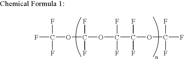
- After the pattern exposure, as shown in FIG. 2C, the resist
film 102 is baked with a hot plate at a temperature of 100° C. for 60 seconds, and the resultant resist film is developed with a 2.38 wt % tetramethylammonium hydroxide developer (alkaline developer). In this manner, a resistpattern 105 made of theunexposed portion 102 b of the resistfilm 102 and having a line width of 0.06 μm can be formed in a good shape as shown in FIG. 2D. - In
Embodiment 1, since thesolution 103 includes water, the surface of the resistfilm 102 can attain affinity owing to the water after the pattern exposure, so that the developer can easily permeate into the resistfilm 102. As a result, the resistpattern 105 can be formed in a good shape. - A pattern formation method according to
Embodiment 2 of the invention will now be described with reference to FIGS. 3A through 3D. - First, a negative chemically amplified resist material having the following composition is prepared:
Base polymer: poly((norbornene-5- 2 g methylenecarboxylic acid) - (maleic anhydride)) (wherein norbornene-5-methylenecarboxylic acid:maleic anhydride = 50 mol %:50 mol %) Crosslinking agent: 1,3,5-N-(trihydroxymethyl)melamine 0.4 g Acid generator: triphenylsulfonium nonaflate 0.06 g Solvent: propylene glycol monomethyl ether acetate 20 g - Next, as shown in FIG. 3A, the aforementioned chemically amplified resist material is applied on a
substrate 201 so as to form a resistfilm 202 with a thickness of 0.20 μm. - Then, as shown in FIG. 3B, while supplying, onto the resist
film 202, anonaqueous solution 203 of perfluoropolyether (having a refractive index n of 1.37) that includes 4 wt % of water and is circulated and temporarily stored in the solution storage 14 (shown in FIG. 1), pattern exposure is carried out by irradiating the resistfilm 202 with exposinglight 204 of F2 laser with NA of 0.60 through a mask not shown. Thus, an exposedportion 202 a of the resistfilm 202 becomes insoluble in an alkaline developer due to the function of the crosslinking agent because an acid is generated from the acid generator therein while anunexposed portion 202 b of the resistfilm 202 remains soluble in an alkaline developer because no acid is generated from the acid generator therein. - After the pattern exposure, as shown in FIG. 3C, the resist
film 202 is baked with a hot plate at a temperature of 110° C. for 60 seconds, and the resultant resist film is developed with a 2.38 wt % tetramethylammonium hydroxide developer (alkaline developer). In this manner, theunexposed portion 202 b of the resistfilm 202 is dissolved in the alkaline developer, and hence, a resistpattern 205 made of the exposedportion 202 a of the resistfilm 202 and having a line width of 0.06 μm can be formed in a good shape as shown in FIG. 3D. - In
Embodiment 2, since thesolution 203 includes water, the surface of the resistfilm 202 can attain affinity owing to the water after the pattern exposure, so that the developer can easily permeate into the resistfilm 202. As a result, the resistpattern 205 can be formed in a good shape. - Although the solution includes 8 wt % of water in
Embodiment Embodiment 2, the amount of water added to the solution is not particularly specified but is generally several wt %. - Also, the chemically amplified resist material is used in
Embodiment - A pattern formation method according to
Embodiment 3 of the invention will now be described with reference to FIGS. 4A through 4D. - First, a positive chemically amplified resist material having the following composition is prepared:
Base polymer: poly((norbornene-5-methylene-t-b 2 g utylcarboxylate) - (maleic anhydride)) (wherein norbornene-5-methylene-t- butylcarboxylate:maleic anhydride = 50 mol %:50 mol %) Acid generator: triphenylsulfonium nonaflate 0.06 g Solvent: propylene glycol monomethyl ether acetate 20 g - Next, as shown in FIG. 4A, the aforementioned chemically amplified resist material is applied on a
substrate 301 so as to form a resistfilm 302 with a thickness of 0.20 μm. - Then, as shown in FIG. 4B, while supplying, onto the resist
film 302, anonaqueous solution 303 of perfluoropolyether (having a refractive index n of 1.37) that includes 6 wt % of 3-methyl-1,2-butanediol, that is, a compound for generating water in the presence of an acid, and is circulated and temporarily stored in the solution storage 14 (shown in FIG. 1), pattern exposure is carried out by irradiating the resistfilm 302 with exposinglight 304 of F2 laser with NA of 0.60 through a mask not shown. Thus, an exposedportion 302 a of the resistfilm 302 becomes soluble in an alkaline developer because an acid is generated from the acid generator therein while anunexposed portion 302 b of the resistfilm 302 remains insoluble in an alkaline developer because no acid is generated from the acid generator therein. - After the pattern exposure, as shown in FIG. 4C, the resist
film 302 is baked with a hot plate at a temperature of 100° C. for 60 seconds, and the resultant resist film is developed with a 2.38 wt % tetramethylammonium hydroxide developer (alkaline developer). In this manner, a resistpattern 305 made of theunexposed portion 302 b of the resistfilm 302 and having a line width of 0.06 μm can be formed in a good shape as shown in FIG. 4D. - In
Embodiment 3, since the resistfilm 302 includes the acid generator and thesolution 303 includes the compound for generating water in the presence of an acid, the surface of the exposedportion 302 a of the resistfilm 302 can attain affinity owing to generated water after the pattern exposure, so that the developer can easily permeate into the exposedportion 302 a of the resistfilm 302. As a result, the resistpattern 305 can be formed in a good shape. - Although the
solution 403 ofEmbodiment 3 includes 6 wt % of the compound for generating water in the presence of an acid, the amount of the compound added to the solution is not particularly specified but is generally several wt %. - A pattern formation method according to
Embodiment 4 of the invention will now be described with reference to FIGS. 5A through 5D. - First, a positive chemically amplified resist material having the following composition is prepared:
Base polymer: poly((norbornene-5-methylene-t- 2 g butylcarboxylate) - (maleic anhydride)) (wherein norbornene-5-methylene-t- butylcarboxylate:maleic anhydride = 50 mol %:50 mol %) Acid generator: triphenylsulfonium nonaflate 0.04 g Solvent: propylene glycol monomethyl ether acetate 20 g - Next, as shown in FIG. 5A, the aforementioned chemically amplified resist material is applied on a
substrate 401 so as to form a resistfilm 402 with a thickness of 0.20 μm. - Then, as shown in FIG. 5B, while supplying, onto the resist
film 402, anonaqueous solution 403 of perfluoropolyether (with a refractive index n of 1.37) that includes 5 wt % of 2,6-dinitrobenzyl tosylate, that is, an acid generator for generating an acid through irradiation with light, and 8 wt % of 2,4-pentanediol, that is, a compound for generating water in the presence of an acid, and is circulated and temporarily stored in the solution storage 14 (shown in FIG. 1), pattern exposure is carried out by irradiating the resistfilm 402 with exposinglight 404 of F2 laser with NA of 0.60 through a mask not shown. Thus, an exposedportion 402 a of the resistfilm 402 becomes soluble in an alkaline developer because an acid is generated from the acid generator therein while anunexposed portion 402 b of the resistfilm 402 remains insoluble in an alkaline developer because no acid is generated from the acid generator therein. - After the pattern exposure, as shown in FIG. 5C, the resist
film 402 is baked with a hot plate at a temperature of 100° C. for 60 seconds, and the resultant resist film is developed with a 2.38 wt % tetramethylammonium hydroxide developer (alkaline developer). In this manner, a resistpattern 405 made of theunexposed portion 402 b of the resistfilm 402 and having a line width of 0.06 μm can be formed in a good shape as shown in FIG. 5D. - In
Embodiment 4, since thesolution 403 includes the acid generator and the compound for generating water in the presence of an acid, the surface of the exposedportion 402 a of the resistfilm 402 can attain affinity owing to generated water after the pattern exposure, so that the developer can easily permeate into the exposedportion 402 a of the resistfilm 402. As a result, the resistpattern 405 can be formed in a good shape. - Although the solution includes 5 wt % of the acid generator and 8 wt % of the compound for generating water in the presence of an acid in
Embodiment 4, the amounts of the acid generator and the compound added to the solution are not particularly specified but are generally several wt %, respectively. - Also, although the positive chemically amplified resist material is used in
Embodiment 4, a positive non-chemically amplified resist material may be used instead. - A pattern formation method according to
Embodiment 5 of the invention will now be described with reference to FIGS. 6A through 6D. - First, a positive chemically amplified resist material having the following composition is prepared:
Base polymer: poly((norbornene-5-methylene-t- 2 g butylcarboxylate) - (maleic anhydride)) (wherein norbornene-5-methylene-t- butylcarboxylate:maleic anhydride = 50 mol %: 50 mol %) Acid generator: triphenylsulfonium nonaflate 0.06 g Solvent: propylene glycol monomethyl ether acetate 20 g - Next, as shown in FIG. 6A, the aforementioned chemically amplified resist material is applied on a
substrate 501 so as to form a resistfilm 502 with a thickness of 0.20 μm. Thereafter, a water-soluble film 503 of a polyvinyl alcohol film including 7 wt % of 2-methyl-2-butanol, that is, a compound for generating water in the presence of an acid, is formed on the resistfilm 502. - Then, as shown in FIG. 6B, while supplying, onto the water-
soluble film 503, asolution 504 of perfluoropolyether that is circulated and temporarily stored in the solution storage 14 (shown in FIG. 1), pattern exposure is carried out by irradiating the water-soluble film 503 and the resistfilm 502 with exposinglight 505 of F2 laser with NA of 0.60 through a mask not shown. Thus, an exposedportion 502 a of the resistfilm 502 becomes soluble in an alkaline developer and water is generated from the water-soluble film 503 in the exposedportion 502 a because an acid is generated from the acid generator therein. On the other hand, anunexposed portion 502 b of the resistfilm 502 remains insoluble in an alkaline developer and no water is generated from the water-soluble film 503 in theunexposed portion 502 b because no acid is generated from the acid generator therein. - After the pattern exposure, as shown in FIG. 6C, the resist
film 502 is baked with a hot plate at a temperature of 100° C. for 60 seconds, and the resultant resist film is developed with a 2.38 wt % tetramethylammonium hydroxide developer (alkaline developer). In this manner, the water-soluble film 503 and the exposedportion 502 a of the resistfilm 502 are dissolved in the alkaline developer, and hence, a resistpattern 505 made of theunexposed portion 502 b of the resistfilm 502 and having a line width of 0.06 μm can be formed in a good shape as shown in FIG. 6D. - In
Embodiment 5, since the resistfilm 502 includes the acid generator and the water-soluble film 503 includes the compound for generating water in the presence of an acid, the surface of the exposedportion 502 a of the resistfilm 502 can attain affinity owing to generated water after the pattern exposure, so that the developer can easily permeate into the exposedportion 502 a of the resistfilm 502. As a result, the resistpattern 505 can be formed in a good shape. - Although the water-
soluble film 503 includes 7 wt % of the compound for generating water in the presence of an acid inEmbodiment 5, the amount of the compound included in the water-soluble film is not particularly specified but is generally several wt %. - A pattern formation method according to
Embodiment 6 of the invention will now be described with reference to FIGS. 7A through 7D. - First, a positive chemically amplified resist material having the following composition is prepared:
Base polymer: poly((norbornene-5-methylene-t- 2 g butylcarboxylate) - (maleic anhydride)) (wherein norbornene-5-methylene-t- butylcarboxylate:maleic anhydride = 50 mol %: 50 mol %) Acid generator: triphenylsulfonium nonaflate 0.045 g Solvent: propylene glycol monomethyl ether acetate 20 g - Next, as shown in FIG. 7A, the aforementioned chemically amplified resist material is applied on a
substrate 601 so as to form a resistfilm 602 with a thickness of 0.20 μm. Thereafter, a water-soluble film 603 of a polyvinyl pyrrolidone film including 4 wt % of N-(trifluoromethylsulfonyloxy)succinimide, that is, an acid generator for generating an acid through irradiation with light, and 5 wt % of benzopinacol, that is, a compound for generating water in the presence of an acid, is formed on the resistfilm 602. - Then, as shown in FIG. 7B, while supplying, onto the water-
soluble film 603, asolution 604 of perfluoropolyether that is circulated and temporarily stored in the solution storage 14 (shown in FIG. 1), pattern exposure is carried out by irradiating the water-soluble film 603 and the resistfilm 602 with exposinglight 605 of F2 laser with NA of 0.60 through a mask not shown. Thus, an exposedportion 602 a of the resistfilm 602 becomes soluble in an alkaline developer because an acid is generated from the acid generator therein while anunexposed portion 602 b of the resistfilm 602 remains insoluble in an alkaline developer because no acid is generated from the acid generator therein. Also, in an exposed portion of the water-soluble film 603, water is generated from the compound because an acid is generated from the acid generator. - After the pattern exposure, as shown in FIG. 7C, the resist
film 602 is baked with a hot plate at a temperature of 100° C. for 60 seconds, and the resultant resist film is developed with a 2.38 wt % tetramethylammonium hydroxide developer (alkaline developer). In this manner, the water-soluble film 603 and the exposedportion 602 a of the resistfilm 602 are dissolved in the alkaline developer, and hence, a resistpattern 605 made of theunexposed portion 602 b of the resistfilm 602 and having a line width of 0.06 μm can be formed in a good shape as shown in FIG. 7D. - In
Embodiment 6, since the water-soluble film 603 includes the acid generator and the compound for generating water in the presence of an acid, the surfaces of the water-soluble film 603 and the resistfilm 602 can attain affinity owing to generated water after the pattern exposure, so that the developer can easily permeate into the exposedportion 602 a of the resistfilm 602. As a result, the resistpattern 605 can be formed in a good shape. - Although the water-
soluble film 603 includes 4 wt % of the acid generator and 5 wt % of the compound for generating water in the presence of an acid inEmbodiment 6, the amounts of the acid generator and the compound included in the water-soluble film 603 are not particularly specified but are generally several wt %, respectively. - Also, although the positive chemically amplified resist material is used in
Embodiment 6, a positive non-chemically amplified resist material may be used instead. - A pattern formation method according to Embodiment 7 of the invention will now be described with reference to FIGS. 8A through 8D.
- First, a positive chemically amplified resist material having the following composition is prepared:
Base polymer: poly((norbornene-5-methylene-t- 2 g butylcarboxylate) - (maleic anhydride)) (wherein norbornene-5-methylene-t- butylcarboxylate:maleic anhydride = 50 mol %: 50 mol %) Acid generator: triphenylsulfonium nonaflate 0.06 g Compound for generating water in the presence of acid: 0.12 g 3-methyl-1,2-butanediol Solvent: propylene glycol monomethyl ether acetate 20 g - Next, as shown in FIG. 8A, the aforementioned chemically amplified resist material is applied on a
substrate 701 so as to form a resistfilm 702 with a thickness of 0.20 μm. - Then, as shown in FIG. 8B, while supplying, onto the resist
film 702, anonaqueous solution 703 of perfluoropolyether (having a refractive index n of 1.37) that is circulated and temporarily stored in the solution storage 14 (shown in FIG. 1), pattern exposure is carried out by irradiating the resistfilm 702 with exposinglight 704 of F2 laser with NA of 0.60 through a mask not shown. Thus, an exposedportion 702 a of the resistfilm 702 becomes soluble in an alkaline developer and water is generated in the exposedportion 702 a because an acid is generated from the acid generator therein. On the other hand, anunexposed portion 702 b of the resistfilm 702 remains insoluble in an alkaline developer and no water is generated in theunexposed portion 702 b because no acid is generated from the acid generator therein. - After the pattern exposure, as shown in FIG. 8C, the resist
film 702 is baked with a hot plate at a temperature of 100° C. for 60 seconds, and the resultant resist film is developed with a 2.38 wt % tetramethylammonium hydroxide developer (alkaline developer). In this manner, a resistpattern 705 made of theunexposed portion 702 b of the resistfilm 702 and having a line width of 0.06 tm can be formed in a good shape as shown in FIG. 8D. - In Embodiment 7, since the resist
film 702 includes the acid generator and the compound for generating water in the presence of an acid, the surface of the exposedportion 702 a of the resistfilm 702 can attain affinity owing to generated water after the pattern exposure, so that the developer can easily permeate into the exposedportion 702 a of the resistfilm 702. As a result, the resistpattern 705 can be formed in a good shape. - The amount of the compound for generating water in the presence of an acid included in the chemically amplified resist material in Embodiment 7 is not particularly specified but is generally several wt %.
- Although F 2 laser is used as the exposing light in each of
Embodiments 1 through 7, another vacuum UV, UV such as a g-line or an i-line, or deep UV such as KrF laser, ArF laser, Kr2 laser, ArKr laser or Ar2 laser can be used instead. - In each of
Embodiments 3 through 7, the solution may include water. Thus, the affinity of the surface of the resist film can be improved, so as to further accelerate the permeation of the developer into the resist film. - In each of
Embodiments 5 through 7, the solution may include a compound for generating water in the presence of an acid. Thus, the affinity of water generated by the acid generated in the exposed portion of the resist film can further accelerate the permeation of the developer into the resist film. - In
Embodiment - In each of
Embodiments 1 through 7, as the acid generator included in the chemically amplified resist material, the solution or the water-soluble film, any of an onium salt, a halogen-containing compound, a diazoketone compound, a diazomethane compound, a sulfone compound, a sulfonic ester compound and a sulfonimide compound can be used. - Examples of the onium salt usable as the acid generator are diphenyliodonium triflate, triphenylsulfonium triflate and triphenylsulfonium nonaflate.
- Examples of the halogen-containing compound usable as the acid generator are 2-phenyl-4,6-bis(trichloromethyl)-s-triazine and 2-naphthyl-4,6-bis(trichloromethyl)-s-triazine.
- Examples of the diazoketone compound usable as the acid generator are 1,3-diphenyldiketo-2-diazopropane, 1,3-dicyclohexyldiketo-2-diazopropane and an ester of 1,2-naphthoquinonediazido-4-sulfonic acid and 2,2,3,4,4′-tetrahydroxybenzophenone.
- Examples of the diazomethane compound usable as the acid generator are bis(trifluoromethylsulfonyl)diazomethane, bis(cyclohexylsulfonyl)diazomethane, bis(phenylsulfonyl)diazomethane, bis(p-tolylsulfonyl)diazomethane and bis(p-chlorophenylsulfonyl)diazomethane.
- Examples of the sulfone compound usable as the acid generator are 4-trisphenacylsulfone, mesitylphenacylsulfone and bis(phenylsulfonyl)methane.
- Examples of the sulfonic ester compound usable as the acid generator are benzoin tosylate, 2,6-dinitrobenzyl tosylate, 2-nitrobenzyl tosylate, 4-nitrobenzyl tosylate and pyrogallol trimesylate.
- Examples of the sulfonimide compound usable as the acid generator are N-(trifluoromethylsulfonyloxy)succinimide, N-(trifluoromethylsulfonyloxy)phthalimide, N-(trifluoromethylsulfonyloxy)diphenylmaleimide, N-(trifluoromethylsulfonyloxy)bicyclo[2.2.1]hepto-5-en-2,3 -dicarboxylimide, N-(trifluoromethylsulfonyloxy)-7-oxabicyclo[2.2.1]hepto-5-en-2,3-dicarboxylimide, N-(trifluoromethylsulfonyloxy)bicyclo[2.2.1]heptane-5,6-oxy-2,3-dicarboxylmide, N-(trifluoromethylsulfonyloxy)naphthyldicarboxylimide, N-(camphorsulfonyloxy)succinimide, N-(camphorsulfonyloxy)phthalimide, N-(camphorsulfonyloxy)diphenylmaleimide, N-(camphorsulfonyloxy)bicyclo[2.2.1]hepto-5-en-2,3-dicarboxylimide, N-(camphorsulfonyloxy)-7-oxabicyclo[2.2.1]hepto-5-en-2,3-dicarboxylimide, N-(camphorsulfonyloxy)bicyclo[2.2.1]heptane-5,6-oxy-2,3-dicarboxylimide, N-(camphorsulfonyloxy)naphthyldicarboxylimide, N-(4-methylphenylsulfonyloxy)succinimide, N-(4-methylphenylsulfonyloxy)phthalimide, N-(4-methylphenylsulfonyloxy)diphenylmaleimide, N-(4-methylphenylsulfonyloxy)bicyclo[2.2.1]hepto-5-en-2,3-dicarboxylimide, N-(4-methylphenylsulfonyloxy)-7-oxabicyclo[2.2.1]hepto-5-en-2,3-dicarboxylimide, N-(4-methylphenylsulfonyloxy)bicyclo[2.2.1]heptane-5,6-oxy-2,3-dicarboxylimide and N-(4-methylphenylsulfonyloxy)naphthyldicarboxylimide.
- In each of
Embodiments 3 through 7, as the compound for generating water in the presence of an acid included in the chemically amplified resist material, the solution or the water-soluble film, a tertiary alcohol, a diol of a tertiary alcohol, a secondary alcohol or a diol of a secondary alcohol can be used. - Examples of the tertiary alcohol usable as the compound for generating water in the presence of an acid are tertiary butanol and 2-methyl-2-butanol.
- Examples of the diol of a tertiary alcohol usable as the compound for generating water in the presence of an acid are 3-methyl-1,3-butanediol and benzopinacol.
- Examples of the secondary alcohol usable as the compound for generating water in the presence of an acid are 2-propanol, 2-butanol and 2-methyl-3-butanol.
- Examples of the diol of a secondary alcohol usable as the compound for generating water in the presence of an acid are 3-methyl-1,2-butanediol and 2,4-pentanediol.
- In
Embodiment
Claims (29)
1. A pattern formation method comprising the steps of:
forming a resist film;
performing pattern exposure by selectively irradiating said resist film with exposing light while supplying, onto said resist film, an immersion solution including a material having an affinity with a developer; and
forming a resist pattern by developing said resist film after the pattern exposure.
2. A pattern formation method comprising the steps of:
forming resist film;
performing pattern exposure by selectively irradiating said resist film with exposing light while supplying, onto said resist film, a nonaqueous solution including water; and
forming a resist pattern by developing said resist film after the pattern exposure.
3. A pattern formation method comprising the steps of:
forming a chemically amplified resist material including an acid generator for generating an acid through irradiation with light;
performing pattern exposure by selectively irradiating said resist film with exposing light while supplying onto said resist film, an immersion solution including a compound for generating a material having an affinity with a developer in the presence of an acid; and
forming a resist pattern by developing said resist film after the pattern exposure.
4. A pattern formation method of claim 3 ,
wherein said chemically amplified resist material includes a compound for generating a material having an affinity with a developer in the presence of an acid.
5. A pattern formation method comprising the steps of:
forming a resist film;
performing pattern exposure by selectively irradiating said resist film with exposing light while supplying, onto said resist film, an immersion solution including an acid generator for generating an acid through irradiation with light and a compound for generating a material having an affinity with a developer in the presence of an acid; and
forming a resist pattern by developing said resist film after the pattern exposure.
6. A pattern formation method comprising the steps of:
forming a chemically amplified resist material including an acid generator for generating an acid through irradiation with light;
forming, on said resist film, a water-soluble film including a compound for generating a material having an affinity with a developer in the presence of an acid;
performing pattern exposure by selectively irradiating said resist film with exposing light while supplying an immersion solution onto said water-soluble film; and
forming a resist pattern by developing said resist film after the pattern exposure.
7. The pattern formation method of claim 6 ,
wherein said immersion solution includes a compound for generating a material having an affinity with a developer in the presence of an acid.
8. The pattern formation method of claim 6 , wherein said chemically amplified resist material includes a compound for generating a material having an affinity with a developer in the presence of acid.
9. A pattern formation method comprising the steps of:
forming a resist film;
forming, on said resist film a water-soluble film including an acid generator for generating an acid through irradiation with light and a compound for generating a material having an affinity with a developer in the presence of an acid;
performing pattern exposure by selectively irradiating said resist film with exposing light while supplying an immersion solution onto said water-soluble film; and
forming a resist pattern by developing said resist film after the pattern exposure.
10. The pattern formation method of claim 9 , wherein said immersion solution includes a compound for generating a material having an affinity with a developer in the presence of acid.
11. A pattern formation method comprising the steps of:
forming a chemically amplified resist material including an acid generator for generating an acid through irradiation with light and a compound for generating a material having an affinity with a developer in the presence of an acid,
performing pattern exposure by selectively irradiating said resist film with exposing light while supplying an immersion solution onto said resist film; and
forming a resist pattern by developing said resist film after the pattern exposure.
12. The pattern formation method of claim 11 , wherein said immersion solution includes a compound for generating a material having an affinity with a developer in the presence of an acid.
13. The pattern formation method of any of claims 1, 2, 3, 5, 6, 9 and 11,
wherein said exposing light is KrF excimer laser, ArF excimer laser, F2 laser, KrAr laser, or Ar2 laser.
14. The pattern formation method of any of claims 1, 2, 3, 5, 6, 9 and 11,
wherein a material having an affinity with a developer is added to said nonaqueous solution.
15. The pattern formation method of any of claims 3, 5, 6, 9 and 11,
wherein said acid generator is an onium salt, a halogen-containing compound, a diazoketone compound, a diazomethane compound, a sulfone compound, a sulfonic ester compound or a sulfonimide compound.
16. The pattern formation method of any of claims 3, 5, 6, 9, and 11,
wherein said acid generator is an onium salt selected from the group consisting of diphenyliodonium triflate, triphenylsulfonium triflate and triphenylsulfonium nonaflate.
17. The pattern formation method of any of claims 3, 5, 6, 9 and 11,
wherein said acid generator is a halogen-containing compound selected from the group consisting of 2-phenyl-4,6-bis(trichloromethyl)-s-triazine and 2-naphthyl-4,6-bis(trichloromethyl)-s-triazine.
18. The pattern formation method of any of claims 3, 5, 6, 9 and 11,
wherein said acid generator is a diazoketone compound selected from the group consisting of 1,3-diphenyldiketo-2-diazopropane, 1,3-dicyclohexyldiketo-2-diazopropane and an ester of 1,2-naphthoquinonediazido-4-sulfonic acid and 2,2,3,4,4′-tetrahydroxybenzophenone.
19. The pattern formation method of any of claims 3, 5, 6, 9 and 11,
wherein said acid generator is a diazomethane compound selected from the group consisting of bis(trifluoromethylsulfonyl)diazomethane, bis(cyclohexylsulfonyl)diazomethane, bis(phenylsulfonyl)diazomethane, bis(p-tolylsulfonyl)diazomethane and bis(p-chlorophenylsulfonyl)diazomethane.
20. The pattern formation method of any of claims 3, 5, 6, 9 and 11,
wherein said acid generator is a sulfone compound selected from the group consisting of 4-trisphenacylsulfone, mesitylphenacylsulfone and bis(phenylsulfonyl)methane.
21. The pattern formation method of any of claims 3, 5, 6, 9 and 11,
wherein said acid generator is a sulfonic ester compound selected from the group consisting of benzoin tosylate, 2,6-dinitrobenzyl tosylate, 2-nitrobenzyl tosylate, 4-nitrobenzyl tosylate and pyrogallol trimesylate.
22. The pattern formation method of any of claims 3, 5, 6, 9 and 11,
wherein said acid generator is a sulfonimide compound selected from the group consisting of N-(trifluoromethylsulfonyloxy)succinimide, N-(trifluoromethylsulfonyloxy)phthalimide, N-(trifluoromethylsulfonyloxy)diphenylmaleimide, N-(trifluoromethylsulfonyloxy)bicyclo[2.2.1]hepto-5-en-2,3-dicarboxylimide, N-(trifluoromethylsulfonyloxy)-7-oxabicyclo[2.2.1]hepto-5-en-2,3-dicarboxylimide, N-(trifluoromethylsulfonyloxy)bicyclo[2.2.1]heptane-5,6-oxy-2,3-dicarboxylmide, N-(trifluoromethylsulfonyloxy)naphthyldicarboxylimide, N-(camphorsulfonyloxy)succinimide, N-(camphorsulfonyloxy)phthalimide, N-(camphorsulfonyloxy)diphenylmaleimide, N-(camphorsulfonyloxy)bicyclo[2.2.1]hepto-5-en-2,3-dicarboxylimide, N-(camphorsulfonyloxy)-7-oxabicyclo[2.2.1]hepto-5-en-2,3dicarboxylimide, N-(camphorsulfonyloxy)bicyclo[2.2.1]heptane-5,6-oxy-2,3dicarboxylimide, N-(camphorsulfonyloxy)naphthyldicarboxylimide, N-(4-methylphenylsulfonyloxy)succinimide, N-(4-methylphenylsulfonyloxy)phthalimide, N-(4-methylphenylsulfonyloxy)diphenylmaleimide, N-(4-methylphenylsulfonyloxy)bicyclo[2.2.1]hepto-5-en-2,3-dicarboxylimide, N-(4-methylphenylsulfonyloxy)-7-oxabicyclo[2.2.1]hepto-5-en-2,3-dicarboxylimide, N-(4-methylphenylsulfonyloxy)bicyclo[2.2.1]heptane-5,6-oxy-2,3-dicarboxylimide and N-(4-methylphenylsulfonyloxy)naphthyldicarboxylimide.
23. The pattern formation method of any of claims 1, 2, 3, 5, 6, 9 and 11,
wherein said material having an affinity with a developer is a tertiary alcohol, a diol of a tertiary alcohol, a secondary alcohol or a diol of a secondary alcohol.
24. The pattern formation method of any of claims 1, 2, 3, 5, 6, 9 and 11,
wherein said material having an affinity with a developer is a tertiary alcohol selected from the group consisting of t-butanol and 2-methyl-2-butanol.
25. The pattern formation method of any of claims 1, 2, 3, 5, 6, 9 and 11,
wherein said material having an affinity with a developer is a diol of a tertiary alcohol selected from the group consisting of 3-methyl-1,3,-butandiol and benzopinacol.
26. The pattern formation method of any of claims 1, 2, 3, 5, 6, 9 and 11,
wherein said material having an affinity with a developer is a secondary alcohol selected from the group consisting of 2-propanol, 2-butanol and 2-methyl-3-butanol.
27. The pattern formation method of any of claims 1, 2, 3, 5, 6, 9 and 11,
wherein said material having an affinity with a developer is a diol of a secondary alcohol selected from the group consisting of 3-methyl-1,2-butandiol and 2,4-pentanediol.
28. The pattern formation method of claim 6 or 9,
wherein said water-soluble film is a polyvinyl alcohol film or a polyvinyl pyrrolidone film.
29. The pattern formation method of any of claims 1, 2, 3, 5, 6, 9 and 11, wherein said immersion solution is perfluoropolyether or water.
Applications Claiming Priority (2)
| Application Number | Priority Date | Filing Date | Title |
|---|---|---|---|
| JP2003-168255 | 2003-06-12 | ||
| JP2003168255A JP4054285B2 (en) | 2003-06-12 | 2003-06-12 | Pattern formation method |
Publications (1)
| Publication Number | Publication Date |
|---|---|
| US20040253547A1 true US20040253547A1 (en) | 2004-12-16 |
Family
ID=33509011
Family Applications (1)
| Application Number | Title | Priority Date | Filing Date |
|---|---|---|---|
| US10/661,540 Abandoned US20040253547A1 (en) | 2003-06-12 | 2003-09-15 | Pattern formation method |
Country Status (3)
| Country | Link |
|---|---|
| US (1) | US20040253547A1 (en) |
| JP (1) | JP4054285B2 (en) |
| CN (1) | CN1574234A (en) |
Cited By (105)
| Publication number | Priority date | Publication date | Assignee | Title |
|---|---|---|---|---|
| US20030120915A1 (en) * | 2001-11-30 | 2003-06-26 | Brocade Communications Systems, Inc. | Node and port authentication in a fibre channel network |
| US20050007569A1 (en) * | 2003-05-13 | 2005-01-13 | Asml Netherlands B.V. | Lithographic apparatus and device manufacturing method |
| US20050128445A1 (en) * | 2003-10-28 | 2005-06-16 | Asml Netherlands B.V. | Lithographic apparatus and device manufacturing method |
| US20050175776A1 (en) * | 2003-11-14 | 2005-08-11 | Asml Netherlands B.V. | Lithographic apparatus and device manufacturing method |
| US20050175940A1 (en) * | 2004-02-11 | 2005-08-11 | Asml Netherlands B.V. | Device manufacturing method and a substrate |
| US20050186516A1 (en) * | 2004-02-25 | 2005-08-25 | Matsushita Electric Industrial Co., Ltd. | Barrier film material and pattern formation method using the same |
| US20050219488A1 (en) * | 2002-12-10 | 2005-10-06 | Nikon Corporation | Exposure apparatus and method for producing device |
| US20050219489A1 (en) * | 2002-12-10 | 2005-10-06 | Nikon Corporation | Exposure apparatus and method for producing device |
| US20050219490A1 (en) * | 2002-12-10 | 2005-10-06 | Nikon Corporation | Exposure apparatus and method for producing device |
| US20050225734A1 (en) * | 2004-04-08 | 2005-10-13 | Asml Netherlands B.V. | Lithographic apparatus and device manufacturing method |
| US20050231694A1 (en) * | 2004-04-14 | 2005-10-20 | Asml Netherlands B.V. | Lithographic apparatus and device manufacturing method |
| US20050237504A1 (en) * | 2002-12-10 | 2005-10-27 | Nikon Corporation | Exposure apparatus, exposure method, and method for producing device |
| US20050259232A1 (en) * | 2004-05-18 | 2005-11-24 | Asml Netherlands B.V. | Lithographic apparatus and device manufacturing method |
| US20050264774A1 (en) * | 2002-12-10 | 2005-12-01 | Nikon Corporation | Exposure apparatus and method for producing device |
| US20050263068A1 (en) * | 2003-10-28 | 2005-12-01 | Asml Netherlands B.V. | Lithographic apparatus |
| US20050280791A1 (en) * | 2003-02-26 | 2005-12-22 | Nikon Corporation | Exposure apparatus, exposure method, and method for producing device |
| US20060012765A1 (en) * | 2003-03-25 | 2006-01-19 | Nikon Corporation | Exposure apparatus and device fabrication method |
| US20060017900A1 (en) * | 2003-04-17 | 2006-01-26 | Nikon Corporation | Optical arrangement of autofocus elements for use with immersion lithography |
| US20060023187A1 (en) * | 2003-04-10 | 2006-02-02 | Nikon Corporation | Environmental system including an electro-osmotic element for an immersion lithography apparatus |
| US20060023181A1 (en) * | 2003-04-10 | 2006-02-02 | Nikon Corporation | Run-off path to collect liquid for an immersion lithography apparatus |
| US20060023184A1 (en) * | 2003-04-09 | 2006-02-02 | Nikon Corporation | Immersion lithography fluid control system |
| US20060023189A1 (en) * | 2002-11-12 | 2006-02-02 | Asml Netherlands B.V. | Lithographic apparatus and device manufacturing method |
| US20060023188A1 (en) * | 2003-04-07 | 2006-02-02 | Nikon Corporation | Exposure apparatus and method for manufacturing device |
| US20060023182A1 (en) * | 2003-04-10 | 2006-02-02 | Nikon Corporation | Environmental system including a transport region for an immersion lithography apparatus |
| US20060023183A1 (en) * | 2003-04-11 | 2006-02-02 | Nikon Corporation | Liquid jet and recovery system for immersion lithography |
| US20060028632A1 (en) * | 2003-04-10 | 2006-02-09 | Nikon Corporation | Environmental system including vacuum scavenge for an immersion lithography apparatus |
| US20060033894A1 (en) * | 2003-04-11 | 2006-02-16 | Nikon Corporation | Apparatus and method for maintaining immersion fluid in the gap under the projection lens during wafer exchange in an immersion lithography machine |
| US20060061747A1 (en) * | 2003-05-15 | 2006-03-23 | Nikon Corporation | Exposure apparatus and device manufacturing method |
| US20060077367A1 (en) * | 2003-05-23 | 2006-04-13 | Nikon Corporation | Exposure apparatus and method for producing device |
| US20060082744A1 (en) * | 2003-05-28 | 2006-04-20 | Nikon Corporation | Exposure method, exposure apparatus, and method for producing device |
| US20060092533A1 (en) * | 2003-07-01 | 2006-05-04 | Nikon Corporation | Using isotopically specified fluids as optical elements |
| US20060098177A1 (en) * | 2003-05-23 | 2006-05-11 | Nikon Corporation | Exposure method, exposure apparatus, and exposure method for producing device |
| US20060103832A1 (en) * | 2003-07-08 | 2006-05-18 | Nikon Corporation | Wafer table for immersion lithography |
| US20060114445A1 (en) * | 2003-06-19 | 2006-06-01 | Nikon Corporation | Exposure apparatus, and device manufacturing method |
| US20060119820A1 (en) * | 2002-12-10 | 2006-06-08 | Nikon Corporation | Exposure apparatus and device manufacturing method |
| US20060119818A1 (en) * | 2003-07-09 | 2006-06-08 | Nikon Corporation | Exposure apparatus and method for manufacturing device |
| US20060146305A1 (en) * | 2003-07-28 | 2006-07-06 | Nikon Corporation | Exposure apparatus, method for producing device, and method for controlling exposure apparatus |
| US20060154183A1 (en) * | 2002-12-10 | 2006-07-13 | Nikon Corporation | Exposure apparatus and method for producing device |
| US20060152697A1 (en) * | 2003-09-03 | 2006-07-13 | Nikon Corporation | Apparatus and method for providing fluid for immersion lithography |
| US20060176456A1 (en) * | 2003-07-09 | 2006-08-10 | Nikon Corporation | Exposure apparatus and device manufacturing method |
| US20060227312A1 (en) * | 2003-06-13 | 2006-10-12 | Nikon Corporation | Exposure method, substrate stage, exposure apparatus, and device manufacturing method |
| US20060232753A1 (en) * | 2005-04-19 | 2006-10-19 | Asml Holding N.V. | Liquid immersion lithography system with tilted liquid flow |
| EP1720073A1 (en) * | 2005-05-03 | 2006-11-08 | ASML Netherlands B.V. | Lithographic apparatus and device manufacturing method |
| US20070031755A1 (en) * | 2003-08-25 | 2007-02-08 | Toko Ohka Kogyo Co., Ltd. | Material for forming resist-protecting film for immersion exposure process, resist-protecting film made of such material, and method for forming resist pattern using such resist-protec- ting film |
| US20070042297A1 (en) * | 2004-12-27 | 2007-02-22 | Eishi Shiobara | Resist pattern forming method and manufacturing method of semiconductor device |
| US20070066452A1 (en) * | 2005-09-22 | 2007-03-22 | William Marshall | Recliner exerciser |
| US20070070316A1 (en) * | 2004-01-20 | 2007-03-29 | Albrecht Ehrmann | Microlithographic projection exposure apparatus and measuring device for a projection lens |
| US20070103655A1 (en) * | 2003-07-28 | 2007-05-10 | Asml Netherlands B.V. | Lithographic apparatus, device manufacturing method and a substrate |
| US20070128482A1 (en) * | 2005-12-06 | 2007-06-07 | Lg Electronics Inc. | Power supply apparatus and method for line connection type fuel cell system |
| US20070171390A1 (en) * | 2003-04-11 | 2007-07-26 | Nikon Corporation | Cleanup method for optics in immersion lithography |
| US20070231741A1 (en) * | 2006-04-04 | 2007-10-04 | Shin-Etsu Chemical Co., Ltd. | Resist composition and patterning process |
| EP1905800A1 (en) * | 2006-09-29 | 2008-04-02 | Samsung Electronics Co., Ltd. | Copolymer, composition for forming banks, and method for forming banks using the composition |
| US7372541B2 (en) | 2002-11-12 | 2008-05-13 | Asml Netherlands B.V. | Lithographic apparatus and device manufacturing method |
| US7394521B2 (en) | 2003-12-23 | 2008-07-01 | Asml Netherlands B.V. | Lithographic apparatus and device manufacturing method |
| US7397533B2 (en) | 2004-12-07 | 2008-07-08 | Asml Netherlands B.V. | Lithographic apparatus and device manufacturing method |
| US7453078B2 (en) | 2005-02-28 | 2008-11-18 | Asml Netherlands B.V. | Sensor for use in a lithographic apparatus |
| US7463330B2 (en) | 2004-07-07 | 2008-12-09 | Asml Netherlands B.V. | Lithographic apparatus and device manufacturing method |
| US7483118B2 (en) | 2003-07-28 | 2009-01-27 | Asml Netherlands B.V. | Lithographic projection apparatus and device manufacturing method |
| US20090040389A1 (en) * | 2007-08-09 | 2009-02-12 | Mstar Semiconductor, Inc | Gamma correction apparatus |
| US7515249B2 (en) | 2003-10-08 | 2009-04-07 | Zao Nikon Co., Ltd. | Substrate carrying apparatus, exposure apparatus, and device manufacturing method |
| US7589822B2 (en) | 2004-02-02 | 2009-09-15 | Nikon Corporation | Stage drive method and stage unit, exposure apparatus, and device manufacturing method |
| US7593092B2 (en) | 2002-11-12 | 2009-09-22 | Asml Netherlands B.V. | Lithographic apparatus and device manufacturing method |
| US20090244514A1 (en) * | 2008-03-26 | 2009-10-01 | Samsung Electronics Co., Ltd. | Distance measuring sensors including vertical photogate and three-dimensional color image sensors including distance measuring sensors |
| US7602470B2 (en) | 2004-08-19 | 2009-10-13 | Asml Netherlands B.V. | Lithographic apparatus and device manufacturing method |
| US20090273766A1 (en) * | 2008-04-11 | 2009-11-05 | Canon Kabushiki Kaisha | Apparatus and method for exposure and method of manufacturing device |
| US7619715B2 (en) | 2003-07-09 | 2009-11-17 | Nikon Corporation | Coupling apparatus, exposure apparatus, and device fabricating method |
| US7684008B2 (en) | 2003-06-11 | 2010-03-23 | Asml Netherlands B.V. | Lithographic apparatus and device manufacturing method |
| US20100182576A1 (en) * | 2003-12-23 | 2010-07-22 | Asml Netherlands B.V. | Lithographic apparatus and device manufacturing method |
| US7779781B2 (en) | 2003-07-31 | 2010-08-24 | Asml Netherlands B.V. | Lithographic apparatus and device manufacturing method |
| US7781763B2 (en) | 2007-08-14 | 2010-08-24 | Samsung Electronics Co., Ltd. | Composition for forming passivation layer and organic thin film transistor comprising the passivation layer |
| US20100297549A1 (en) * | 2008-11-19 | 2010-11-25 | Rohm And Haas Electronic Materials Llc | Compositions comprising hetero-substituted carbocyclic aryl component and processes for photolithography |
| US7843550B2 (en) | 2003-07-25 | 2010-11-30 | Nikon Corporation | Projection optical system inspecting method and inspection apparatus, and a projection optical system manufacturing method |
| US7880860B2 (en) | 2004-12-20 | 2011-02-01 | Asml Netherlands B.V. | Lithographic apparatus and device manufacturing method |
| US7898645B2 (en) | 2003-10-08 | 2011-03-01 | Zao Nikon Co., Ltd. | Substrate transport apparatus and method, exposure apparatus and exposure method, and device fabricating method |
| US7907255B2 (en) | 2003-08-29 | 2011-03-15 | Asml Netherlands B.V. | Lithographic apparatus and device manufacturing method |
| US7924402B2 (en) | 2003-09-19 | 2011-04-12 | Nikon Corporation | Exposure apparatus and device manufacturing method |
| US7924403B2 (en) | 2005-01-14 | 2011-04-12 | Asml Netherlands B.V. | Lithographic apparatus and device and device manufacturing method |
| US7982857B2 (en) | 2003-12-15 | 2011-07-19 | Nikon Corporation | Stage apparatus, exposure apparatus, and exposure method with recovery device having lyophilic portion |
| US7990517B2 (en) | 2004-02-03 | 2011-08-02 | Nikon Corporation | Immersion exposure apparatus and device manufacturing method with residual liquid detector |
| US7995186B2 (en) | 2003-10-08 | 2011-08-09 | Zao Nikon Co., Ltd. | Substrate conveyance device and substrate conveyance method, exposure apparatus and exposure method, device manufacturing method |
| US8039807B2 (en) | 2003-09-29 | 2011-10-18 | Nikon Corporation | Exposure apparatus, exposure method, and method for producing device |
| US8054447B2 (en) | 2003-12-03 | 2011-11-08 | Nikon Corporation | Exposure apparatus, exposure method, method for producing device, and optical part |
| US8054448B2 (en) | 2004-05-04 | 2011-11-08 | Nikon Corporation | Apparatus and method for providing fluid for immersion lithography |
| US8111373B2 (en) | 2004-03-25 | 2012-02-07 | Nikon Corporation | Exposure apparatus and device fabrication method |
| US8120763B2 (en) | 2002-12-20 | 2012-02-21 | Carl Zeiss Smt Gmbh | Device and method for the optical measurement of an optical system by using an immersion fluid |
| US8130361B2 (en) | 2003-10-09 | 2012-03-06 | Nikon Corporation | Exposure apparatus, exposure method, and method for producing device |
| US20120077122A1 (en) * | 2010-09-28 | 2012-03-29 | Fujifilm Corporation | Pattern forming method, chemical amplification resist composition and resist film |
| US8154708B2 (en) | 2003-06-09 | 2012-04-10 | Asml Netherlands B.V. | Lithographic apparatus and device manufacturing method |
| US8237911B2 (en) | 2007-03-15 | 2012-08-07 | Nikon Corporation | Apparatus and methods for keeping immersion fluid adjacent to an optical assembly during wafer exchange in an immersion lithography machine |
| USRE43576E1 (en) | 2005-04-08 | 2012-08-14 | Asml Netherlands B.V. | Dual stage lithographic apparatus and device manufacturing method |
| US8305553B2 (en) | 2004-08-18 | 2012-11-06 | Nikon Corporation | Exposure apparatus and device manufacturing method |
| US8363206B2 (en) | 2006-05-09 | 2013-01-29 | Carl Zeiss Smt Gmbh | Optical imaging device with thermal attenuation |
| US8384874B2 (en) | 2004-07-12 | 2013-02-26 | Nikon Corporation | Immersion exposure apparatus and device manufacturing method to detect if liquid on base member |
| US8520184B2 (en) | 2004-06-09 | 2013-08-27 | Nikon Corporation | Immersion exposure apparatus and device manufacturing method with measuring device |
| US8654305B2 (en) | 2007-02-15 | 2014-02-18 | Asml Holding N.V. | Systems and methods for insitu lens cleaning in immersion lithography |
| US8692973B2 (en) | 2005-01-31 | 2014-04-08 | Nikon Corporation | Exposure apparatus and method for producing device |
| US8817226B2 (en) | 2007-02-15 | 2014-08-26 | Asml Holding N.V. | Systems and methods for insitu lens cleaning using ozone in immersion lithography |
| US8941810B2 (en) | 2005-12-30 | 2015-01-27 | Asml Netherlands B.V. | Lithographic apparatus and device manufacturing method |
| US9176393B2 (en) | 2008-05-28 | 2015-11-03 | Asml Netherlands B.V. | Lithographic apparatus and a method of operating the apparatus |
| US9223224B2 (en) | 2003-08-29 | 2015-12-29 | Nikon Corporation | Exposure apparatus with component from which liquid is protected and/or removed and device fabricating method |
| US9256136B2 (en) | 2010-04-22 | 2016-02-09 | Asml Netherlands B.V. | Fluid handling structure, lithographic apparatus and device manufacturing method involving gas supply |
| US9429495B2 (en) | 2004-06-04 | 2016-08-30 | Carl Zeiss Smt Gmbh | System for measuring the image quality of an optical imaging system |
| US9482966B2 (en) | 2002-11-12 | 2016-11-01 | Asml Netherlands B.V. | Lithographic apparatus and device manufacturing method |
| US9746781B2 (en) | 2005-01-31 | 2017-08-29 | Nikon Corporation | Exposure apparatus and method for producing device |
| US10503084B2 (en) | 2002-11-12 | 2019-12-10 | Asml Netherlands B.V. | Lithographic apparatus and device manufacturing method |
-
2003
- 2003-06-12 JP JP2003168255A patent/JP4054285B2/en not_active Expired - Fee Related
- 2003-09-15 US US10/661,540 patent/US20040253547A1/en not_active Abandoned
-
2004
- 2004-05-17 CN CNA2004100447172A patent/CN1574234A/en active Pending
Cited By (559)
| Publication number | Priority date | Publication date | Assignee | Title |
|---|---|---|---|---|
| US20030120915A1 (en) * | 2001-11-30 | 2003-06-26 | Brocade Communications Systems, Inc. | Node and port authentication in a fibre channel network |
| US9366972B2 (en) | 2002-11-12 | 2016-06-14 | Asml Netherlands B.V. | Lithographic apparatus and device manufacturing method |
| US8797503B2 (en) | 2002-11-12 | 2014-08-05 | Asml Netherlands B.V. | Lithographic apparatus and device manufacturing method with a liquid inlet above an aperture of a liquid confinement structure |
| US10788755B2 (en) | 2002-11-12 | 2020-09-29 | Asml Netherlands B.V. | Lithographic apparatus and device manufacturing method |
| US9091940B2 (en) | 2002-11-12 | 2015-07-28 | Asml Netherlands B.V. | Lithographic apparatus and method involving a fluid inlet and a fluid outlet |
| US10620545B2 (en) | 2002-11-12 | 2020-04-14 | Asml Netherlands B.V. | Lithographic apparatus and device manufacturing method |
| US7593092B2 (en) | 2002-11-12 | 2009-09-22 | Asml Netherlands B.V. | Lithographic apparatus and device manufacturing method |
| US7593093B2 (en) | 2002-11-12 | 2009-09-22 | Asml Netherlands B.V. | Lithographic apparatus and device manufacturing method |
| US8558989B2 (en) | 2002-11-12 | 2013-10-15 | Asml Netherlands B.V. | Lithographic apparatus and device manufacturing method |
| US7388648B2 (en) | 2002-11-12 | 2008-06-17 | Asml Netherlands B.V. | Lithographic projection apparatus |
| US10962891B2 (en) | 2002-11-12 | 2021-03-30 | Asml Netherlands B.V. | Lithographic apparatus and device manufacturing method |
| US8472002B2 (en) | 2002-11-12 | 2013-06-25 | Asml Netherlands B.V. | Lithographic apparatus and device manufacturing method |
| US10261428B2 (en) | 2002-11-12 | 2019-04-16 | Asml Netherlands B.V. | Lithographic apparatus and device manufacturing method |
| US9482966B2 (en) | 2002-11-12 | 2016-11-01 | Asml Netherlands B.V. | Lithographic apparatus and device manufacturing method |
| US10222706B2 (en) | 2002-11-12 | 2019-03-05 | Asml Netherlands B.V. | Lithographic apparatus and device manufacturing method |
| US9740107B2 (en) | 2002-11-12 | 2017-08-22 | Asml Netherlands B.V. | Lithographic apparatus and device manufacturing method |
| US10503084B2 (en) | 2002-11-12 | 2019-12-10 | Asml Netherlands B.V. | Lithographic apparatus and device manufacturing method |
| US7372541B2 (en) | 2002-11-12 | 2008-05-13 | Asml Netherlands B.V. | Lithographic apparatus and device manufacturing method |
| US8208120B2 (en) | 2002-11-12 | 2012-06-26 | Asml Netherlands B.V. | Lithographic apparatus and device manufacturing method |
| US9057967B2 (en) | 2002-11-12 | 2015-06-16 | Asml Netherlands B.V. | Lithographic apparatus and device manufacturing method |
| US7982850B2 (en) | 2002-11-12 | 2011-07-19 | Asml Netherlands B.V. | Immersion lithographic apparatus and device manufacturing method with gas supply |
| US20060023189A1 (en) * | 2002-11-12 | 2006-02-02 | Asml Netherlands B.V. | Lithographic apparatus and device manufacturing method |
| US10191389B2 (en) | 2002-11-12 | 2019-01-29 | Asml Netherlands B.V. | Lithographic apparatus and device manufacturing method |
| US20060132736A1 (en) * | 2002-12-10 | 2006-06-22 | Nikon Corporation | Exposure apparatus, exposure method, and method for producing device |
| US20070171391A1 (en) * | 2002-12-10 | 2007-07-26 | Nikon Corporation | Exposure apparatus and method for producing device |
| US7446851B2 (en) | 2002-12-10 | 2008-11-04 | Nikon Corporation | Exposure apparatus and device manufacturing method |
| US8294876B2 (en) | 2002-12-10 | 2012-10-23 | Nikon Corporation | Exposure apparatus and device manufacturing method |
| US7589820B2 (en) | 2002-12-10 | 2009-09-15 | Nikon Corporation | Exposure apparatus and method for producing device |
| US7460207B2 (en) | 2002-12-10 | 2008-12-02 | Nikon Corporation | Exposure apparatus and method for producing device |
| US20070258063A1 (en) * | 2002-12-10 | 2007-11-08 | Nikon Corporation | Exposure apparatus, exposure method, and method for producing device |
| US8004650B2 (en) | 2002-12-10 | 2011-08-23 | Nikon Corporation | Exposure apparatus and device manufacturing method |
| US20050219488A1 (en) * | 2002-12-10 | 2005-10-06 | Nikon Corporation | Exposure apparatus and method for producing device |
| US7515246B2 (en) | 2002-12-10 | 2009-04-07 | Nikon Corporation | Exposure apparatus, exposure method, and method for producing device |
| US20050219489A1 (en) * | 2002-12-10 | 2005-10-06 | Nikon Corporation | Exposure apparatus and method for producing device |
| US20060098178A1 (en) * | 2002-12-10 | 2006-05-11 | Nikon Corporation | Exposure apparatus, exposure method, and method for producing device |
| US7436487B2 (en) | 2002-12-10 | 2008-10-14 | Nikon Corporation | Exposure apparatus and method for producing device |
| US7466392B2 (en) | 2002-12-10 | 2008-12-16 | Nikon Corporation | Exposure apparatus, exposure method, and method for producing device |
| US7436486B2 (en) | 2002-12-10 | 2008-10-14 | Nikon Corporation | Exposure apparatus and device manufacturing method |
| US7948604B2 (en) | 2002-12-10 | 2011-05-24 | Nikon Corporation | Exposure apparatus and method for producing device |
| US20060119820A1 (en) * | 2002-12-10 | 2006-06-08 | Nikon Corporation | Exposure apparatus and device manufacturing method |
| US20060152699A1 (en) * | 2002-12-10 | 2006-07-13 | Nikon Corporation | Exposure apparatus and method for producing device |
| US20060126043A1 (en) * | 2002-12-10 | 2006-06-15 | Nikon Corporation | Exposure apparatus and method for producing device |
| US20060126044A1 (en) * | 2002-12-10 | 2006-06-15 | Nikon Corporation | Exposure apparatus and method for producing device |
| US20060132738A1 (en) * | 2002-12-10 | 2006-06-22 | Nikon Corporation | Exposure apparatus and device manufacturing method |
| US20050219490A1 (en) * | 2002-12-10 | 2005-10-06 | Nikon Corporation | Exposure apparatus and method for producing device |
| US8089611B2 (en) | 2002-12-10 | 2012-01-03 | Nikon Corporation | Exposure apparatus and method for producing device |
| US7589821B2 (en) | 2002-12-10 | 2009-09-15 | Nikon Corporation | Exposure apparatus and device manufacturing method |
| US7639343B2 (en) | 2002-12-10 | 2009-12-29 | Nikon Corporation | Exposure apparatus and device manufacturing method |
| US20060154183A1 (en) * | 2002-12-10 | 2006-07-13 | Nikon Corporation | Exposure apparatus and method for producing device |
| US7242455B2 (en) | 2002-12-10 | 2007-07-10 | Nikon Corporation | Exposure apparatus and method for producing device |
| US8034539B2 (en) | 2002-12-10 | 2011-10-11 | Nikon Corporation | Exposure apparatus and method for producing device |
| US20060164615A1 (en) * | 2002-12-10 | 2006-07-27 | Nikon Corporation | Exposure apparatus and device manufacturing method |
| US20050237504A1 (en) * | 2002-12-10 | 2005-10-27 | Nikon Corporation | Exposure apparatus, exposure method, and method for producing device |
| US7817244B2 (en) | 2002-12-10 | 2010-10-19 | Nikon Corporation | Exposure apparatus and method for producing device |
| US7911582B2 (en) | 2002-12-10 | 2011-03-22 | Nikon Corporation | Exposure apparatus and device manufacturing method |
| US20050264774A1 (en) * | 2002-12-10 | 2005-12-01 | Nikon Corporation | Exposure apparatus and method for producing device |
| US20070263196A1 (en) * | 2002-12-10 | 2007-11-15 | Nikon Corporation | Exposure apparatus and device manufacturing method |
| US20070115448A1 (en) * | 2002-12-10 | 2007-05-24 | Nikon Corporation | Exposure apparatus and device manufacturing method |
| US20070115447A1 (en) * | 2002-12-10 | 2007-05-24 | Nikon Corporation | Exposure apparatus and device manufacturing method |
| US20060250596A1 (en) * | 2002-12-10 | 2006-11-09 | Nikon Corporation | Exposure apparatus and method for producing device |
| US7379158B2 (en) | 2002-12-10 | 2008-05-27 | Nikon Corporation | Exposure apparatus and method for producing device |
| US20060274294A1 (en) * | 2002-12-10 | 2006-12-07 | Nikon Corporation | Exposure apparatus, exposure method, and method for producing device |
| US20070024832A1 (en) * | 2002-12-10 | 2007-02-01 | Nikon Corporation | Exposure apparatus and method for producing device |
| US7834976B2 (en) | 2002-12-10 | 2010-11-16 | Nikon Corporation | Exposure apparatus and method for producing device |
| US20070035710A1 (en) * | 2002-12-10 | 2007-02-15 | Nikon Corporation | Exposure apparatus, exposure method, and method for producing device |
| US20070035711A1 (en) * | 2002-12-10 | 2007-02-15 | Nikon Corporation | Exposure apparatus and method for producing device |
| US20090079950A1 (en) * | 2002-12-10 | 2009-03-26 | Nikon Corporation | Exposure apparatus, exposure method, and method for producing device |
| US7505111B2 (en) | 2002-12-10 | 2009-03-17 | Nikon Corporation | Exposure apparatus and device manufacturing method |
| US8836929B2 (en) | 2002-12-20 | 2014-09-16 | Carl Zeiss Smt Gmbh | Device and method for the optical measurement of an optical system by using an immersion fluid |
| US8120763B2 (en) | 2002-12-20 | 2012-02-21 | Carl Zeiss Smt Gmbh | Device and method for the optical measurement of an optical system by using an immersion fluid |
| US20050280791A1 (en) * | 2003-02-26 | 2005-12-22 | Nikon Corporation | Exposure apparatus, exposure method, and method for producing device |
| US20070263186A1 (en) * | 2003-02-26 | 2007-11-15 | Nikon Corporation | Exposure apparatus, exposure method, and method for producing device |
| US7932991B2 (en) | 2003-02-26 | 2011-04-26 | Nikon Corporation | Exposure apparatus, exposure method, and method for producing device |
| US7542128B2 (en) | 2003-02-26 | 2009-06-02 | Nikon Corporation | Exposure apparatus, exposure method, and method for producing device |
| US9348239B2 (en) | 2003-02-26 | 2016-05-24 | Nikon Corporation | Exposure apparatus, exposure method, and method for producing device |
| US7911583B2 (en) | 2003-02-26 | 2011-03-22 | Nikon Corporation | Exposure apparatus, exposure method, and method for producing device |
| US9182684B2 (en) | 2003-02-26 | 2015-11-10 | Nikon Corporation | Exposure apparatus, exposure method, and method for producing device |
| US7535550B2 (en) | 2003-02-26 | 2009-05-19 | Nikon Corporation | Exposure apparatus, exposure method, and method for producing device |
| US7907253B2 (en) | 2003-02-26 | 2011-03-15 | Nikon Corporation | Exposure apparatus, exposure method, and method for producing device |
| US20070258065A1 (en) * | 2003-02-26 | 2007-11-08 | Nikon Corporation | Exposure apparatus, exposure method, and method for producing device |
| US8102504B2 (en) | 2003-02-26 | 2012-01-24 | Nikon Corporation | Exposure apparatus, exposure method, and method for producing device |
| US20070258067A1 (en) * | 2003-02-26 | 2007-11-08 | Nikon Corporation | Exposure apparatus, exposure method, and method for producing device |
| US10180632B2 (en) | 2003-02-26 | 2019-01-15 | Nikon Corporation | Exposure apparatus, exposure method, and method for producing device |
| US7907254B2 (en) | 2003-02-26 | 2011-03-15 | Nikon Corporation | Exposure apparatus, exposure method, and method for producing device |
| US8736809B2 (en) | 2003-02-26 | 2014-05-27 | Nikon Corporation | Exposure apparatus, exposure method, and method for producing device |
| US7268854B2 (en) | 2003-02-26 | 2007-09-11 | Nikon Corporation | Exposure apparatus, exposure method, and method for producing device |
| US9766555B2 (en) | 2003-02-26 | 2017-09-19 | Nikon Corporation | Exposure apparatus, exposure method, and method for producing device |
| US7453550B2 (en) | 2003-02-26 | 2008-11-18 | Nikon Corporation | Exposure apparatus, exposure method, and method for producing device |
| US7916272B2 (en) | 2003-03-25 | 2011-03-29 | Nikon Corporation | Exposure apparatus and device fabrication method |
| US20060012765A1 (en) * | 2003-03-25 | 2006-01-19 | Nikon Corporation | Exposure apparatus and device fabrication method |
| US20060268249A1 (en) * | 2003-03-25 | 2006-11-30 | Nikon Corporation | Exposure apparatus and device fabrication method |
| US7471371B2 (en) | 2003-03-25 | 2008-12-30 | Nikon Corporation | Exposure apparatus and device fabrication method |
| US8804095B2 (en) | 2003-03-25 | 2014-08-12 | Nikon Corporation | Exposure apparatus and device fabrication method |
| US20070109516A1 (en) * | 2003-03-25 | 2007-05-17 | Nikon Corporation | Exposure apparatus and device fabrication method |
| US8558987B2 (en) | 2003-03-25 | 2013-10-15 | Nikon Corporation | Exposure apparatus and device fabrication method |
| US8018570B2 (en) | 2003-03-25 | 2011-09-13 | Nikon Corporation | Exposure apparatus and device fabrication method |
| US8537331B2 (en) | 2003-04-07 | 2013-09-17 | Nikon Corporation | Exposure apparatus and method for manufacturing device |
| US20080291410A1 (en) * | 2003-04-07 | 2008-11-27 | Nikon Corporation | Exposure apparatus and method for manufacturing device |
| US20060023188A1 (en) * | 2003-04-07 | 2006-02-02 | Nikon Corporation | Exposure apparatus and method for manufacturing device |
| US8111375B2 (en) | 2003-04-07 | 2012-02-07 | Nikon Corporation | Exposure apparatus and method for manufacturing device |
| US7480029B2 (en) | 2003-04-07 | 2009-01-20 | Nikon Corporation | Exposure apparatus and method for manufacturing device |
| US20060033901A1 (en) * | 2003-04-07 | 2006-02-16 | Nikon Corporation | Exposure apparatus and method for manufacturing device |
| US20070263184A1 (en) * | 2003-04-09 | 2007-11-15 | Nikon Corporation | Immersion lithography fluid control system |
| US20060023184A1 (en) * | 2003-04-09 | 2006-02-02 | Nikon Corporation | Immersion lithography fluid control system |
| US20070268468A1 (en) * | 2003-04-09 | 2007-11-22 | Nikon Corporation | Immersion lithography fluid control system |
| US7339650B2 (en) | 2003-04-09 | 2008-03-04 | Nikon Corporation | Immersion lithography fluid control system that applies force to confine the immersion liquid |
| US8797500B2 (en) | 2003-04-09 | 2014-08-05 | Nikon Corporation | Immersion lithography fluid control system changing flow velocity of gas outlets based on motion of a surface |
| US8497973B2 (en) | 2003-04-09 | 2013-07-30 | Nikon Corporation | Immersion lithography fluid control system regulating gas velocity based on contact angle |
| US20070115453A1 (en) * | 2003-04-09 | 2007-05-24 | Nikon Corporation | Immersion lithography fluid control system |
| US9618852B2 (en) | 2003-04-09 | 2017-04-11 | Nikon Corporation | Immersion lithography fluid control system regulating flow velocity of gas based on position of gas outlets |
| US8102501B2 (en) | 2003-04-09 | 2012-01-24 | Nikon Corporation | Immersion lithography fluid control system using an electric or magnetic field generator |
| US20090075211A1 (en) * | 2003-04-09 | 2009-03-19 | Nikon Corporation | Immersion lithography fluid control system |
| US20090075212A1 (en) * | 2003-04-09 | 2009-03-19 | Nikon Corporation | Immersion lithography fluid control system |
| US7965376B2 (en) | 2003-04-10 | 2011-06-21 | Nikon Corporation | Environmental system including a transport region for an immersion lithography apparatus |
| US7345742B2 (en) | 2003-04-10 | 2008-03-18 | Nikon Corporation | Environmental system including a transport region for an immersion lithography apparatus |
| US7321415B2 (en) | 2003-04-10 | 2008-01-22 | Nikon Corporation | Environmental system including vacuum scavenge for an immersion lithography apparatus |
| US9244362B2 (en) | 2003-04-10 | 2016-01-26 | Nikon Corporation | Environmental system including vacuum scavenge for an immersion lithography apparatus |
| US9244363B2 (en) | 2003-04-10 | 2016-01-26 | Nikon Corporation | Environmental system including a transport region for an immersion lithography apparatus |
| US20070247603A1 (en) * | 2003-04-10 | 2007-10-25 | Nikon Corporation | Environmental system including vacuum scavenge for an immersion lithography apparatus |
| US7355676B2 (en) | 2003-04-10 | 2008-04-08 | Nikon Corporation | Environmental system including vacuum scavenge for an immersion lithography apparatus |
| US7251017B2 (en) | 2003-04-10 | 2007-07-31 | Nikon Corporation | Environmental system including a transport region for an immersion lithography apparatus |
| US20070139631A1 (en) * | 2003-04-10 | 2007-06-21 | Nikon Corporation | Environmental system including a transport region for an immersion lithography apparatus |
| US20070103662A1 (en) * | 2003-04-10 | 2007-05-10 | Nikon Corporation | Environmental system including vacuum scavenge for an immersion lithography apparatus |
| US8456610B2 (en) | 2003-04-10 | 2013-06-04 | Nikon Corporation | Environmental system including vacuum scavenge for an immersion lithography apparatus |
| US8243253B2 (en) | 2003-04-10 | 2012-08-14 | Nikon Corporation | Lyophobic run-off path to collect liquid for an immersion lithography apparatus |
| US9632427B2 (en) | 2003-04-10 | 2017-04-25 | Nikon Corporation | Environmental system including a transport region for an immersion lithography apparatus |
| US9658537B2 (en) | 2003-04-10 | 2017-05-23 | Nikon Corporation | Environmental system including vacuum scavenge for an immersion lithography apparatus |
| US9910370B2 (en) | 2003-04-10 | 2018-03-06 | Nikon Corporation | Environmental system including a transport region for an immersion lithography apparatus |
| US7929110B2 (en) | 2003-04-10 | 2011-04-19 | Nikon Corporation | Environmental system including a transport region for an immersion lithography apparatus |
| US9007561B2 (en) | 2003-04-10 | 2015-04-14 | Nikon Corporation | Immersion lithography apparatus with hydrophilic region encircling hydrophobic region which encircles substrate support |
| US7397532B2 (en) | 2003-04-10 | 2008-07-08 | Nikon Corporation | Run-off path to collect liquid for an immersion lithography apparatus |
| US9977350B2 (en) | 2003-04-10 | 2018-05-22 | Nikon Corporation | Environmental system including vacuum scavenge for an immersion lithography apparatus |
| US8810768B2 (en) | 2003-04-10 | 2014-08-19 | Nikon Corporation | Environmental system including vacuum scavenge for an immersion lithography apparatus |
| US8830443B2 (en) | 2003-04-10 | 2014-09-09 | Nikon Corporation | Environmental system including a transport region for an immersion lithography apparatus |
| US8836914B2 (en) | 2003-04-10 | 2014-09-16 | Nikon Corporation | Environmental system including vacuum scavenge for an immersion lithography apparatus |
| US7929111B2 (en) | 2003-04-10 | 2011-04-19 | Nikon Corporation | Environmental system including a transport region for an immersion lithography apparatus |
| US20080239261A1 (en) * | 2003-04-10 | 2008-10-02 | Nikon Corporation | Run-off path to collect liquid for an immersion lithography apparatus |
| US20060114435A1 (en) * | 2003-04-10 | 2006-06-01 | Nikon Corporation | Environmental system including vacuum scavenge for an immersion lithography apparatus |
| US7969552B2 (en) | 2003-04-10 | 2011-06-28 | Nikon Corporation | Environmental system including a transport region for an immersion lithography apparatus |
| US20060033899A1 (en) * | 2003-04-10 | 2006-02-16 | Nikon Corporation | Environmental system including vacuum scavenge for an immersion lithography apparatus |
| US20060028632A1 (en) * | 2003-04-10 | 2006-02-09 | Nikon Corporation | Environmental system including vacuum scavenge for an immersion lithography apparatus |
| US20060023182A1 (en) * | 2003-04-10 | 2006-02-02 | Nikon Corporation | Environmental system including a transport region for an immersion lithography apparatus |
| US20060023181A1 (en) * | 2003-04-10 | 2006-02-02 | Nikon Corporation | Run-off path to collect liquid for an immersion lithography apparatus |
| US7456930B2 (en) | 2003-04-10 | 2008-11-25 | Nikon Corporation | Environmental system including vacuum scavenge for an immersion lithography apparatus |
| US20060023187A1 (en) * | 2003-04-10 | 2006-02-02 | Nikon Corporation | Environmental system including an electro-osmotic element for an immersion lithography apparatus |
| US8089610B2 (en) | 2003-04-10 | 2012-01-03 | Nikon Corporation | Environmental system including vacuum scavenge for an immersion lithography apparatus |
| US9081298B2 (en) | 2003-04-11 | 2015-07-14 | Nikon Corporation | Apparatus for maintaining immersion fluid in the gap under the projection lens during wafer exchange using a co-planar member in an immersion lithography machine |
| US8514367B2 (en) | 2003-04-11 | 2013-08-20 | Nikon Corporation | Apparatus and method for maintaining immersion fluid in the gap under the projection lens during wafer exchange in an immersion lithography machine |
| US8879047B2 (en) | 2003-04-11 | 2014-11-04 | Nikon Corporation | Apparatus and method for maintaining immersion fluid in the gap under the projection lens using a pad member or second stage during wafer exchange in an immersion lithography machine |
| US8085381B2 (en) | 2003-04-11 | 2011-12-27 | Nikon Corporation | Cleanup method for optics in immersion lithography using sonic device |
| US8848166B2 (en) | 2003-04-11 | 2014-09-30 | Nikon Corporation | Apparatus and method for maintaining immersion fluid in the gap under the projection lens during wafer exchange in an immersion lithography machine |
| US7443482B2 (en) | 2003-04-11 | 2008-10-28 | Nikon Corporation | Liquid jet and recovery system for immersion lithography |
| US8351019B2 (en) | 2003-04-11 | 2013-01-08 | Nikon Corporation | Apparatus and method for maintaining immersion fluid in the gap under the projection lens during wafer exchange in an immersion lithography machine |
| US8269946B2 (en) | 2003-04-11 | 2012-09-18 | Nikon Corporation | Cleanup method for optics in immersion lithography supplying cleaning liquid at different times than immersion liquid |
| US8269944B2 (en) | 2003-04-11 | 2012-09-18 | Nikon Corporation | Apparatus and method for maintaining immersion fluid in the gap under the projection lens during wafer exchange in an immersion lithography machine |
| US20110031416A1 (en) * | 2003-04-11 | 2011-02-10 | Nikon Corporation | Liquid jet and recovery system for immersion lithography |
| US9785057B2 (en) | 2003-04-11 | 2017-10-10 | Nikon Corporation | Liquid jet and recovery system for immersion lithography |
| US9946163B2 (en) | 2003-04-11 | 2018-04-17 | Nikon Corporation | Apparatus and method for maintaining immersion fluid in the gap under the projection lens during wafer exchange in an immersion lithography machine |
| US9958786B2 (en) | 2003-04-11 | 2018-05-01 | Nikon Corporation | Cleanup method for optics in immersion lithography using object on wafer holder in place of wafer |
| US8035795B2 (en) | 2003-04-11 | 2011-10-11 | Nikon Corporation | Apparatus and method for maintaining immersion fluid in the gap under the protection lens during wafer exchange in an immersion lithography machine |
| US8848168B2 (en) | 2003-04-11 | 2014-09-30 | Nikon Corporation | Apparatus and method for maintaining immersion fluid in the gap under the projection lens during wafer exchange in an immersion lithography machine |
| US8488100B2 (en) | 2003-04-11 | 2013-07-16 | Nikon Corporation | Apparatus and method for maintaining immersion fluid in the gap under the projection lens during wafer exchange in an immersion lithography machine |
| US8059258B2 (en) | 2003-04-11 | 2011-11-15 | Nikon Corporation | Liquid jet and recovery system for immersion lithography |
| US7372538B2 (en) | 2003-04-11 | 2008-05-13 | Nikon Corporation | Apparatus and method for maintaining immerison fluid in the gap under the projection lens during wafer exchange in an immersion lithography machine |
| US8493545B2 (en) | 2003-04-11 | 2013-07-23 | Nikon Corporation | Cleanup method for optics in immersion lithography supplying cleaning liquid onto a surface of object below optical element, liquid supply port and liquid recovery port |
| US20070171390A1 (en) * | 2003-04-11 | 2007-07-26 | Nikon Corporation | Cleanup method for optics in immersion lithography |
| US9500960B2 (en) | 2003-04-11 | 2016-11-22 | Nikon Corporation | Apparatus and method for maintaining immersion fluid in the gap under the projection lens during wafer exchange in an immersion lithography machine |
| US7522259B2 (en) | 2003-04-11 | 2009-04-21 | Nikon Corporation | Cleanup method for optics in immersion lithography |
| US20060023183A1 (en) * | 2003-04-11 | 2006-02-02 | Nikon Corporation | Liquid jet and recovery system for immersion lithography |
| US7932989B2 (en) | 2003-04-11 | 2011-04-26 | Nikon Corporation | Liquid jet and recovery system for immersion lithography |
| US9329493B2 (en) | 2003-04-11 | 2016-05-03 | Nikon Corporation | Apparatus and method for maintaining immersion fluid in the gap under the projection lens during wafer exchange in an immersion lithography machine |
| US20060033894A1 (en) * | 2003-04-11 | 2006-02-16 | Nikon Corporation | Apparatus and method for maintaining immersion fluid in the gap under the projection lens during wafer exchange in an immersion lithography machine |
| US7545479B2 (en) | 2003-04-11 | 2009-06-09 | Nikon Corporation | Apparatus and method for maintaining immersion fluid in the gap under the projection lens during wafer exchange in an immersion lithography machine |
| US7327435B2 (en) | 2003-04-11 | 2008-02-05 | Nikon Corporation | Apparatus and method for maintaining immersion fluid in the gap under the projection lens during wafer exchange in an immersion lithography machine |
| US20070216886A1 (en) * | 2003-04-11 | 2007-09-20 | Nikon Corporation | Apparatus and method for maintaining immersion fluid in the gap under the projection lens during wafer exchange in an immersion lithography machine |
| US9304409B2 (en) | 2003-04-11 | 2016-04-05 | Nikon Corporation | Liquid jet and recovery system for immersion lithography |
| US8610875B2 (en) | 2003-04-11 | 2013-12-17 | Nikon Corporation | Apparatus and method for maintaining immersion fluid in the gap under the projection lens during wafer exchange in an immersion lithography machine |
| US8634057B2 (en) | 2003-04-11 | 2014-01-21 | Nikon Corporation | Apparatus and method for maintaining immersion fluid in the gap under the projection lens during wafer exchange in an immersion lithography machine |
| US8670103B2 (en) | 2003-04-11 | 2014-03-11 | Nikon Corporation | Cleanup method for optics in immersion lithography using bubbles |
| US10185222B2 (en) | 2003-04-11 | 2019-01-22 | Nikon Corporation | Liquid jet and recovery system for immersion lithography |
| US8670104B2 (en) | 2003-04-11 | 2014-03-11 | Nikon Corporation | Cleanup method for optics in immersion lithography with cleaning liquid opposed by a surface of object |
| US20070247601A1 (en) * | 2003-04-11 | 2007-10-25 | Nikon Corporation | Cleanup method for optics in immersion lithography |
| US20060017900A1 (en) * | 2003-04-17 | 2006-01-26 | Nikon Corporation | Optical arrangement of autofocus elements for use with immersion lithography |
| US9086636B2 (en) | 2003-04-17 | 2015-07-21 | Nikon Corporation | Optical arrangement of autofocus elements for use with immersion lithography |
| US7414794B2 (en) | 2003-04-17 | 2008-08-19 | Nikon Corporation | Optical arrangement of autofocus elements for use with immersion lithography |
| US8953250B2 (en) | 2003-04-17 | 2015-02-10 | Nikon Corporation | Optical arrangement of autofocus elements for use with immersion lithography |
| US8599488B2 (en) | 2003-04-17 | 2013-12-03 | Nikon Corporation | Optical arrangement of autofocus elements for use with immersion lithography |
| US20070076303A1 (en) * | 2003-04-17 | 2007-04-05 | Nikon Corporation | Optical arrangement of autofocus elements for use with immersion lithography |
| US20090317751A1 (en) * | 2003-04-17 | 2009-12-24 | Nikon Corporation | Optical arrangement of autofocus elements for use with immersion lithography |
| US7570431B2 (en) | 2003-04-17 | 2009-08-04 | Nikon Corporation | Optical arrangement of autofocus elements for use with immersion lithography |
| US8810915B2 (en) | 2003-04-17 | 2014-08-19 | Nikon Corporation | Optical arrangement of autofocus elements for use with immersion lithography |
| US8018657B2 (en) | 2003-04-17 | 2011-09-13 | Nikon Corporation | Optical arrangement of autofocus elements for use with immersion lithography |
| US8094379B2 (en) | 2003-04-17 | 2012-01-10 | Nikon Corporation | Optical arrangement of autofocus elements for use with immersion lithography |
| US9798246B2 (en) | 2003-05-13 | 2017-10-24 | Asml Netherlands B.V. | Lithographic apparatus and device manufacturing method |
| US9477160B2 (en) | 2003-05-13 | 2016-10-25 | Asml Netherland B.V. | Lithographic apparatus and device manufacturing method |
| US7936444B2 (en) | 2003-05-13 | 2011-05-03 | Asml Netherlands B.V. | Lithographic apparatus and device manufacturing method |
| US8724083B2 (en) | 2003-05-13 | 2014-05-13 | Asml Netherlands B.V. | Lithographic apparatus and device manufacturing method |
| US10466595B2 (en) | 2003-05-13 | 2019-11-05 | Asml Netherlands B.V. | Lithographic apparatus and device manufacturing method |
| US20080218717A1 (en) * | 2003-05-13 | 2008-09-11 | Asml Netherlands B.V. | Lithographic apparatus and device manufacturing method |
| US8964164B2 (en) | 2003-05-13 | 2015-02-24 | Asml Netherlands B.V. | Lithographic apparatus and device manufacturing method |
| US20050007569A1 (en) * | 2003-05-13 | 2005-01-13 | Asml Netherlands B.V. | Lithographic apparatus and device manufacturing method |
| US20110181859A1 (en) * | 2003-05-13 | 2011-07-28 | Asml Netherlands B.V. | Lithographic apparatus and device manufacturing method |
| US7352434B2 (en) | 2003-05-13 | 2008-04-01 | Asml Netherlands B.V. | Lithographic apparatus and device manufacturing method |
| US8724084B2 (en) | 2003-05-13 | 2014-05-13 | Asml Netherlands B.V. | Lithographic apparatus and device manufacturing method |
| US7385674B2 (en) | 2003-05-15 | 2008-06-10 | Nikon Corporation | Exposure apparatus and device manufacturing method |
| US7359034B2 (en) | 2003-05-15 | 2008-04-15 | Nikon Corporation | Exposure apparatus and device manufacturing method |
| US20060152698A1 (en) * | 2003-05-15 | 2006-07-13 | Nikon Corporation | Exposure apparatus and device manufacturing method |
| US20060061747A1 (en) * | 2003-05-15 | 2006-03-23 | Nikon Corporation | Exposure apparatus and device manufacturing method |
| US8488108B2 (en) | 2003-05-23 | 2013-07-16 | Nikon Corporation | Exposure method, exposure apparatus, and method for producing device |
| US9977336B2 (en) | 2003-05-23 | 2018-05-22 | Nikon Corporation | Exposure method, exposure apparatus, and method for producing device |
| US8384877B2 (en) | 2003-05-23 | 2013-02-26 | Nikon Corporation | Exposure apparatus and method for producing device |
| US8780327B2 (en) | 2003-05-23 | 2014-07-15 | Nikon Corporation | Exposure apparatus and method for producing device |
| US8072576B2 (en) | 2003-05-23 | 2011-12-06 | Nikon Corporation | Exposure apparatus and method for producing device |
| US20060077367A1 (en) * | 2003-05-23 | 2006-04-13 | Nikon Corporation | Exposure apparatus and method for producing device |
| US8125612B2 (en) | 2003-05-23 | 2012-02-28 | Nikon Corporation | Exposure apparatus and method for producing device |
| US20070121089A1 (en) * | 2003-05-23 | 2007-05-31 | Nikon Corporation | Exposure method, exposure apparatus, and method for producing device |
| US9933708B2 (en) | 2003-05-23 | 2018-04-03 | Nikon Corporation | Exposure method, exposure apparatus, and method for producing device |
| US9939739B2 (en) | 2003-05-23 | 2018-04-10 | Nikon Corporation | Exposure apparatus and method for producing device |
| US8472001B2 (en) | 2003-05-23 | 2013-06-25 | Nikon Corporation | Exposure method, exposure apparatus, and method for producing device |
| US20090009745A1 (en) * | 2003-05-23 | 2009-01-08 | Nikon Corporation | Exposure method, exposure apparatus, and method for producing device |
| US8134682B2 (en) | 2003-05-23 | 2012-03-13 | Nikon Corporation | Exposure apparatus and method for producing device |
| US8174668B2 (en) | 2003-05-23 | 2012-05-08 | Nikon Corporation | Exposure apparatus and method for producing device |
| US7495744B2 (en) | 2003-05-23 | 2009-02-24 | Nikon Corporation | Exposure method, exposure apparatus, and method for producing device |
| US8760617B2 (en) | 2003-05-23 | 2014-06-24 | Nikon Corporation | Exposure apparatus and method for producing device |
| US7388649B2 (en) | 2003-05-23 | 2008-06-17 | Nikon Corporation | Exposure apparatus and method for producing device |
| US9354525B2 (en) | 2003-05-23 | 2016-05-31 | Nikon Corporation | Exposure method, exposure apparatus, and method for producing device |
| US9304392B2 (en) | 2003-05-23 | 2016-04-05 | Nikon Corporation | Exposure apparatus and method for producing device |
| US8169592B2 (en) | 2003-05-23 | 2012-05-01 | Nikon Corporation | Exposure apparatus and method for producing device |
| US7399979B2 (en) | 2003-05-23 | 2008-07-15 | Nikon Corporation | Exposure method, exposure apparatus, and method for producing device |
| US9285684B2 (en) | 2003-05-23 | 2016-03-15 | Nikon Corporation | Exposure method, exposure apparatus, and method for producing device |
| US20060098177A1 (en) * | 2003-05-23 | 2006-05-11 | Nikon Corporation | Exposure method, exposure apparatus, and exposure method for producing device |
| US20060098179A1 (en) * | 2003-05-28 | 2006-05-11 | Nikon Corporation | Exposure method, exposure apparatus, and method for producing device |
| US10082739B2 (en) | 2003-05-28 | 2018-09-25 | Nikon Corporation | Exposure method, exposure apparatus, and method for producing device |
| US8711324B2 (en) | 2003-05-28 | 2014-04-29 | Nikon Corporation | Exposure method, exposure apparatus, and method for producing device |
| US7483117B2 (en) | 2003-05-28 | 2009-01-27 | Nikon Corporation | Exposure method, exposure apparatus, and method for producing device |
| US9488920B2 (en) | 2003-05-28 | 2016-11-08 | Nikon Corporation | Exposure method, exposure apparatus, and method for producing device |
| US20060082744A1 (en) * | 2003-05-28 | 2006-04-20 | Nikon Corporation | Exposure method, exposure apparatus, and method for producing device |
| US8233133B2 (en) | 2003-05-28 | 2012-07-31 | Nikon Corporation | Exposure method, exposure apparatus, and method for producing device |
| US8421992B2 (en) | 2003-05-28 | 2013-04-16 | Nikon Corporation | Exposure method, exposure apparatus, and method for producing device |
| US8482845B2 (en) | 2003-06-09 | 2013-07-09 | Asml Netherlands B.V. | Lithographic apparatus and device manufacturing method |
| US9152058B2 (en) | 2003-06-09 | 2015-10-06 | Asml Netherlands B.V. | Lithographic apparatus and device manufacturing method involving a member and a fluid opening |
| US9081299B2 (en) | 2003-06-09 | 2015-07-14 | Asml Netherlands B.V. | Lithographic apparatus and device manufacturing method involving removal of liquid entering a gap |
| US8154708B2 (en) | 2003-06-09 | 2012-04-10 | Asml Netherlands B.V. | Lithographic apparatus and device manufacturing method |
| US10180629B2 (en) | 2003-06-09 | 2019-01-15 | Asml Netherlands B.V. | Lithographic apparatus and device manufacturing method |
| US10678139B2 (en) | 2003-06-09 | 2020-06-09 | Asml Netherlands B.V. | Lithographic apparatus and device manufacturing method |
| US9541843B2 (en) | 2003-06-09 | 2017-01-10 | Asml Netherlands B.V. | Lithographic apparatus and device manufacturing method involving a sensor detecting a radiation beam through liquid |
| US9110389B2 (en) | 2003-06-11 | 2015-08-18 | Asml Netherlands B.V. | Lithographic apparatus and device manufacturing method |
| US7684008B2 (en) | 2003-06-11 | 2010-03-23 | Asml Netherlands B.V. | Lithographic apparatus and device manufacturing method |
| US9964858B2 (en) | 2003-06-11 | 2018-05-08 | Asml Netherlands B.V. | Lithographic apparatus and device manufacturing method |
| US8363208B2 (en) | 2003-06-11 | 2013-01-29 | Asml Netherlands B.V. | Lithographic apparatus and device manufacturing method |
| US8208117B2 (en) | 2003-06-13 | 2012-06-26 | Nikon Corporation | Exposure method, substrate stage, exposure apparatus, and device manufacturing method |
| US7483119B2 (en) | 2003-06-13 | 2009-01-27 | Nikon Corporation | Exposure method, substrate stage, exposure apparatus, and device manufacturing method |
| US8384880B2 (en) | 2003-06-13 | 2013-02-26 | Nikon Corporation | Exposure method, substrate stage, exposure apparatus, and device manufacturing method |
| US20060227312A1 (en) * | 2003-06-13 | 2006-10-12 | Nikon Corporation | Exposure method, substrate stage, exposure apparatus, and device manufacturing method |
| US20090015816A1 (en) * | 2003-06-13 | 2009-01-15 | Nikon Corporation | Exposure method, substrate stage, exposure apparatus, and device manufacturing method |
| US9268237B2 (en) | 2003-06-13 | 2016-02-23 | Nikon Corporation | Exposure method, substrate stage, exposure apparatus, and device manufacturing method |
| US8040491B2 (en) | 2003-06-13 | 2011-10-18 | Nikon Corporation | Exposure method, substrate stage, exposure apparatus, and device manufacturing method |
| US9019467B2 (en) | 2003-06-13 | 2015-04-28 | Nikon Corporation | Exposure method, substrate stage, exposure apparatus, and device manufacturing method |
| US9846371B2 (en) | 2003-06-13 | 2017-12-19 | Nikon Corporation | Exposure method, substrate stage, exposure apparatus, and device manufacturing method |
| US7486385B2 (en) | 2003-06-19 | 2009-02-03 | Nikon Corporation | Exposure apparatus, and device manufacturing method |
| US8018575B2 (en) | 2003-06-19 | 2011-09-13 | Nikon Corporation | Exposure apparatus, and device manufacturing method |
| US9001307B2 (en) | 2003-06-19 | 2015-04-07 | Nikon Corporation | Exposure apparatus and device manufacturing method |
| US10007188B2 (en) | 2003-06-19 | 2018-06-26 | Nikon Corporation | Exposure apparatus and device manufacturing method |
| US9810995B2 (en) | 2003-06-19 | 2017-11-07 | Nikon Corporation | Exposure apparatus and device manufacturing method |
| US9019473B2 (en) | 2003-06-19 | 2015-04-28 | Nikon Corporation | Exposure apparatus and device manufacturing method |
| US8436979B2 (en) | 2003-06-19 | 2013-05-07 | Nikon Corporation | Exposure apparatus, and device manufacturing method |
| US20060132739A1 (en) * | 2003-06-19 | 2006-06-22 | Nikon Corporation | Exposure apparatus, and device manufacturing method |
| US8705001B2 (en) | 2003-06-19 | 2014-04-22 | Nikon Corporation | Exposure apparatus, and device manufacturing method |
| US8436978B2 (en) | 2003-06-19 | 2013-05-07 | Nikon Corporation | Exposure apparatus, and device manufacturing method |
| US8830445B2 (en) | 2003-06-19 | 2014-09-09 | Nikon Corporation | Exposure apparatus, and device manufacturing method |
| US9274437B2 (en) | 2003-06-19 | 2016-03-01 | Nikon Corporation | Exposure apparatus and device manufacturing method |
| US7321419B2 (en) | 2003-06-19 | 2008-01-22 | Nikon Corporation | Exposure apparatus, and device manufacturing method |
| US8027027B2 (en) | 2003-06-19 | 2011-09-27 | Nikon Corporation | Exposure apparatus, and device manufacturing method |
| US9025129B2 (en) | 2003-06-19 | 2015-05-05 | Nikon Corporation | Exposure apparatus, and device manufacturing method |
| US7812925B2 (en) | 2003-06-19 | 2010-10-12 | Nikon Corporation | Exposure apparatus, and device manufacturing method |
| US8767177B2 (en) | 2003-06-19 | 2014-07-01 | Nikon Corporation | Exposure apparatus, and device manufacturing method |
| US20060114445A1 (en) * | 2003-06-19 | 2006-06-01 | Nikon Corporation | Exposure apparatus, and device manufacturing method |
| US20070064214A1 (en) * | 2003-06-19 | 2007-03-22 | Nikon Corporation | Exposure apparatus, and device manufacturing method |
| US8319941B2 (en) | 2003-06-19 | 2012-11-27 | Nikon Corporation | Exposure apparatus, and device manufacturing method |
| US9551943B2 (en) | 2003-06-19 | 2017-01-24 | Nikon Corporation | Exposure apparatus and device manufacturing method |
| US8724085B2 (en) | 2003-06-19 | 2014-05-13 | Nikon Corporation | Exposure apparatus, and device manufacturing method |
| US8692976B2 (en) | 2003-06-19 | 2014-04-08 | Nikon Corporation | Exposure apparatus, and device manufacturing method |
| US10191388B2 (en) | 2003-06-19 | 2019-01-29 | Nikon Corporation | Exposure apparatus, and device manufacturing method |
| US8717537B2 (en) | 2003-06-19 | 2014-05-06 | Nikon Corporation | Exposure apparatus, and device manufacturing method |
| US20070053090A1 (en) * | 2003-07-01 | 2007-03-08 | Nikon Corporation | Using isotopically specified fluids as optical elements |
| US7236232B2 (en) | 2003-07-01 | 2007-06-26 | Nikon Corporation | Using isotopically specified fluids as optical elements |
| US20060092533A1 (en) * | 2003-07-01 | 2006-05-04 | Nikon Corporation | Using isotopically specified fluids as optical elements |
| US7224435B2 (en) | 2003-07-01 | 2007-05-29 | Nikon Corporation | Using isotopically specified fluids as optical elements |
| US20070195302A1 (en) * | 2003-07-01 | 2007-08-23 | Nikon Corporation | Using isotopically specified fluids as optical elements |
| US8508718B2 (en) | 2003-07-08 | 2013-08-13 | Nikon Corporation | Wafer table having sensor for immersion lithography |
| US7486380B2 (en) | 2003-07-08 | 2009-02-03 | Nikon Corporation | Wafer table for immersion lithography |
| US7301607B2 (en) | 2003-07-08 | 2007-11-27 | Nikon Corporation | Wafer table for immersion lithography |
| US20070076182A1 (en) * | 2003-07-08 | 2007-04-05 | Nikon Corporation | Wafer table for immersion lithography |
| US20060103832A1 (en) * | 2003-07-08 | 2006-05-18 | Nikon Corporation | Wafer table for immersion lithography |
| US20060119818A1 (en) * | 2003-07-09 | 2006-06-08 | Nikon Corporation | Exposure apparatus and method for manufacturing device |
| US20100007865A1 (en) * | 2003-07-09 | 2010-01-14 | Nikon Corporation | Coupling apparatus, exposure apparatus, and device fabricating method |
| US7855777B2 (en) | 2003-07-09 | 2010-12-21 | Nikon Corporation | Exposure apparatus and method for manufacturing device |
| US7580114B2 (en) | 2003-07-09 | 2009-08-25 | Nikon Corporation | Exposure apparatus and method for manufacturing device |
| US8228484B2 (en) | 2003-07-09 | 2012-07-24 | Nikon Corporation | Coupling apparatus, exposure apparatus, and device fabricating method |
| US8218127B2 (en) | 2003-07-09 | 2012-07-10 | Nikon Corporation | Exposure apparatus and device manufacturing method |
| US7619715B2 (en) | 2003-07-09 | 2009-11-17 | Nikon Corporation | Coupling apparatus, exposure apparatus, and device fabricating method |
| US9977352B2 (en) | 2003-07-09 | 2018-05-22 | Nikon Corporation | Exposure apparatus and device manufacturing method |
| US7508490B2 (en) | 2003-07-09 | 2009-03-24 | Nikon Corporation | Exposure apparatus and device manufacturing method |
| US20060176456A1 (en) * | 2003-07-09 | 2006-08-10 | Nikon Corporation | Exposure apparatus and device manufacturing method |
| US8797505B2 (en) | 2003-07-09 | 2014-08-05 | Nikon Corporation | Exposure apparatus and device manufacturing method |
| US9500959B2 (en) | 2003-07-09 | 2016-11-22 | Nikon Corporation | Exposure apparatus and device manufacturing method |
| US8120751B2 (en) | 2003-07-09 | 2012-02-21 | Nikon Corporation | Coupling apparatus, exposure apparatus, and device fabricating method |
| US8879043B2 (en) | 2003-07-09 | 2014-11-04 | Nikon Corporation | Exposure apparatus and method for manufacturing device |
| US20080018873A1 (en) * | 2003-07-09 | 2008-01-24 | Nikon Corporation | Exposure apparatus and method for manufacturing device |
| US9097988B2 (en) | 2003-07-09 | 2015-08-04 | Nikon Corporation | Exposure apparatus and device manufacturing method |
| US7379157B2 (en) | 2003-07-09 | 2008-05-27 | Nikon Corproation | Exposure apparatus and method for manufacturing device |
| US7868997B2 (en) | 2003-07-25 | 2011-01-11 | Nikon Corporation | Projection optical system inspecting method and inspection apparatus, and a projection optical system manufacturing method |
| US7843550B2 (en) | 2003-07-25 | 2010-11-30 | Nikon Corporation | Projection optical system inspecting method and inspection apparatus, and a projection optical system manufacturing method |
| US10185232B2 (en) | 2003-07-28 | 2019-01-22 | Nikon Corporation | Exposure apparatus, method for producing device, and method for controlling exposure apparatus |
| US8964163B2 (en) | 2003-07-28 | 2015-02-24 | Asml Netherlands B.V. | Immersion lithographic apparatus and device manufacturing method with a projection system having a part movable relative to another part |
| US7746445B2 (en) | 2003-07-28 | 2010-06-29 | Asml Netherlands B.V. | Lithographic apparatus, device manufacturing method and a substrate |
| US8749757B2 (en) | 2003-07-28 | 2014-06-10 | Nikon Corporation | Exposure apparatus, method for producing device, and method for controlling exposure apparatus |
| US7505115B2 (en) | 2003-07-28 | 2009-03-17 | Nikon Corporation | Exposure apparatus, method for producing device, and method for controlling exposure apparatus |
| US9760026B2 (en) | 2003-07-28 | 2017-09-12 | Nikon Corporation | Exposure apparatus, method for producing device, and method for controlling exposure apparatus |
| US20060146305A1 (en) * | 2003-07-28 | 2006-07-06 | Nikon Corporation | Exposure apparatus, method for producing device, and method for controlling exposure apparatus |
| US7483118B2 (en) | 2003-07-28 | 2009-01-27 | Asml Netherlands B.V. | Lithographic projection apparatus and device manufacturing method |
| US8451424B2 (en) | 2003-07-28 | 2013-05-28 | Nikon Corporation | Exposure apparatus, method for producing device, and method for controlling exposure apparatus |
| US9639006B2 (en) | 2003-07-28 | 2017-05-02 | Asml Netherlands B.V. | Lithographic projection apparatus and device manufacturing method |
| US10303066B2 (en) | 2003-07-28 | 2019-05-28 | Asml Netherlands B.V. | Lithographic projection apparatus and device manufacturing method |
| US8218125B2 (en) | 2003-07-28 | 2012-07-10 | Asml Netherlands B.V. | Immersion lithographic apparatus with a projection system having an isolated or movable part |
| US20070103655A1 (en) * | 2003-07-28 | 2007-05-10 | Asml Netherlands B.V. | Lithographic apparatus, device manufacturing method and a substrate |
| US9494871B2 (en) | 2003-07-28 | 2016-11-15 | Nikon Corporation | Exposure apparatus, method for producing device, and method for controlling exposure apparatus |
| US7779781B2 (en) | 2003-07-31 | 2010-08-24 | Asml Netherlands B.V. | Lithographic apparatus and device manufacturing method |
| US8142852B2 (en) | 2003-07-31 | 2012-03-27 | Asml Netherlands B.V. | Lithographic apparatus and device manufacturing method |
| US9285686B2 (en) | 2003-07-31 | 2016-03-15 | Asml Netherlands B.V. | Lithographic apparatus involving an immersion liquid supply system with an aperture |
| US8937704B2 (en) | 2003-07-31 | 2015-01-20 | Asml Netherlands B.V. | Lithographic apparatus and device manufacturing method involving a resistivity sensor |
| US20070031755A1 (en) * | 2003-08-25 | 2007-02-08 | Toko Ohka Kogyo Co., Ltd. | Material for forming resist-protecting film for immersion exposure process, resist-protecting film made of such material, and method for forming resist pattern using such resist-protec- ting film |
| US7907255B2 (en) | 2003-08-29 | 2011-03-15 | Asml Netherlands B.V. | Lithographic apparatus and device manufacturing method |
| US8947637B2 (en) | 2003-08-29 | 2015-02-03 | Asml Netherlands B.V. | Lithographic apparatus and device manufacturing method |
| US10514618B2 (en) | 2003-08-29 | 2019-12-24 | Asml Netherlands B.V. | Lithographic apparatus and device manufacturing method |
| US10025204B2 (en) | 2003-08-29 | 2018-07-17 | Asml Netherlands B.V. | Lithographic apparatus and device manufacturing method |
| US9316919B2 (en) | 2003-08-29 | 2016-04-19 | Asml Netherlands B.V. | Lithographic apparatus and device manufacturing method |
| US8035798B2 (en) | 2003-08-29 | 2011-10-11 | Asml Netherlands B.V. | Lithographic apparatus and device manufacturing method |
| US11003096B2 (en) | 2003-08-29 | 2021-05-11 | Asml Netherlands B.V. | Lithographic apparatus and device manufacturing method |
| US9223224B2 (en) | 2003-08-29 | 2015-12-29 | Nikon Corporation | Exposure apparatus with component from which liquid is protected and/or removed and device fabricating method |
| US9568841B2 (en) | 2003-08-29 | 2017-02-14 | Asml Netherlands B.V. | Lithographic apparatus and device manufacturing method |
| US20060152697A1 (en) * | 2003-09-03 | 2006-07-13 | Nikon Corporation | Apparatus and method for providing fluid for immersion lithography |
| US9547243B2 (en) | 2003-09-03 | 2017-01-17 | Nikon Corporation | Apparatus and method for providing fluid for immersion lithography |
| US8520187B2 (en) | 2003-09-03 | 2013-08-27 | Nikon Corporation | Apparatus and method for providing fluid for immersion lithography |
| US9817319B2 (en) | 2003-09-03 | 2017-11-14 | Nikon Corporation | Apparatus and method for providing fluid for immersion lithography |
| US8896807B2 (en) | 2003-09-03 | 2014-11-25 | Nikon Corporation | Apparatus and method for providing fluid for immersion lithography |
| US10203610B2 (en) | 2003-09-03 | 2019-02-12 | Nikon Corporation | Apparatus and method for providing fluid for immersion lithography |
| US7292313B2 (en) | 2003-09-03 | 2007-11-06 | Nikon Corporation | Apparatus and method for providing fluid for immersion lithography |
| US7924402B2 (en) | 2003-09-19 | 2011-04-12 | Nikon Corporation | Exposure apparatus and device manufacturing method |
| US8039807B2 (en) | 2003-09-29 | 2011-10-18 | Nikon Corporation | Exposure apparatus, exposure method, and method for producing device |
| US8749759B2 (en) | 2003-09-29 | 2014-06-10 | Nikon Corporation | Exposure apparatus, exposure method, and method for producing device |
| US10025194B2 (en) | 2003-09-29 | 2018-07-17 | Nikon Corporation | Exposure apparatus, exposure method, and method for producing device |
| US8305552B2 (en) | 2003-09-29 | 2012-11-06 | Nikon Corporation | Exposure apparatus, exposure method, and method for producing device |
| US8139198B2 (en) | 2003-09-29 | 2012-03-20 | Nikon Corporation | Exposure apparatus, exposure method, and method for producing device |
| US9513558B2 (en) | 2003-09-29 | 2016-12-06 | Nikon Corporation | Exposure apparatus, exposure method, and method for producing device |
| US7898645B2 (en) | 2003-10-08 | 2011-03-01 | Zao Nikon Co., Ltd. | Substrate transport apparatus and method, exposure apparatus and exposure method, and device fabricating method |
| US7995186B2 (en) | 2003-10-08 | 2011-08-09 | Zao Nikon Co., Ltd. | Substrate conveyance device and substrate conveyance method, exposure apparatus and exposure method, device manufacturing method |
| US9097986B2 (en) | 2003-10-08 | 2015-08-04 | Nikon Corporation | Substrate conveyance device and substrate conveyance method, exposure apparatus and exposure method, device manufacturing method |
| US9110381B2 (en) | 2003-10-08 | 2015-08-18 | Nikon Corporation | Substrate conveyance device and substrate conveyance method, exposure apparatus and exposure method, device manufacturing method |
| US8755025B2 (en) | 2003-10-08 | 2014-06-17 | Nikon Corporation | Substrate transport apparatus and method, exposure apparatus and exposure method, and device fabricating method |
| US8345216B2 (en) | 2003-10-08 | 2013-01-01 | Nikon Corporation | Substrate conveyance device and substrate conveyance method, exposure apparatus and exposure method, device manufacturing method |
| US8107055B2 (en) | 2003-10-08 | 2012-01-31 | Zao Nikon Co., Ltd. | Substrate conveyance device and substrate conveyance method, exposure apparatus and exposure method, device manufacturing method |
| US7515249B2 (en) | 2003-10-08 | 2009-04-07 | Zao Nikon Co., Ltd. | Substrate carrying apparatus, exposure apparatus, and device manufacturing method |
| US8130361B2 (en) | 2003-10-09 | 2012-03-06 | Nikon Corporation | Exposure apparatus, exposure method, and method for producing device |
| US10209623B2 (en) | 2003-10-09 | 2019-02-19 | Nikon Corporation | Exposure apparatus, exposure method, and method for producing device |
| US9383656B2 (en) | 2003-10-09 | 2016-07-05 | Nikon Corporation | Exposure apparatus, exposure method, and method for producing device |
| US9063438B2 (en) | 2003-10-09 | 2015-06-23 | Nikon Corporation | Exposure apparatus, exposure method, and method for producing device |
| US8638418B2 (en) | 2003-10-28 | 2014-01-28 | Asml Netherlands B.V. | Lithographic apparatus |
| US9182679B2 (en) | 2003-10-28 | 2015-11-10 | Asml Netherlands B.V. | Lithographic apparatus and device manufacturing method |
| US8542344B2 (en) | 2003-10-28 | 2013-09-24 | Asml Netherlands B.V. | Lithographic apparatus and device manufacturing method |
| US20050128445A1 (en) * | 2003-10-28 | 2005-06-16 | Asml Netherlands B.V. | Lithographic apparatus and device manufacturing method |
| US7532304B2 (en) | 2003-10-28 | 2009-05-12 | Asml Netherlands B.V. | Lithographic apparatus and device manufacturing method |
| US8542343B2 (en) | 2003-10-28 | 2013-09-24 | Asml Netherlands B.V. | Lithographic apparatus |
| US8102502B2 (en) | 2003-10-28 | 2012-01-24 | Asml Netherlands B.V. | Lithographic apparatus and device manufacturing method |
| US10248034B2 (en) | 2003-10-28 | 2019-04-02 | Asml Netherlands B.V. | Lithographic apparatus and device manufacturing method |
| US8810771B2 (en) | 2003-10-28 | 2014-08-19 | Asml Netherlands B.V. | Lithographic apparatus and device manufacturing method |
| US20050263068A1 (en) * | 2003-10-28 | 2005-12-01 | Asml Netherlands B.V. | Lithographic apparatus |
| US7411653B2 (en) | 2003-10-28 | 2008-08-12 | Asml Netherlands B.V. | Lithographic apparatus |
| US8860922B2 (en) | 2003-10-28 | 2014-10-14 | Asml Netherlands B.V. | Lithographic apparatus and device manufacturing method |
| US9482962B2 (en) | 2003-10-28 | 2016-11-01 | Asml Netherlands B.V. | Lithographic apparatus and device manufacturing method |
| US7868998B2 (en) | 2003-10-28 | 2011-01-11 | Asml Netherlands B.V. | Lithographic apparatus |
| US8860923B2 (en) | 2003-10-28 | 2014-10-14 | Asml Netherlands B.V. | Lithographic apparatus and device manufacturing method |
| US10527955B2 (en) | 2003-10-28 | 2020-01-07 | Asml Netherlands B.V. | Lithographic apparatus and device manufacturing method |
| US7352433B2 (en) | 2003-10-28 | 2008-04-01 | Asml Netherlands B.V. | Lithographic apparatus and device manufacturing method |
| US9134622B2 (en) | 2003-11-14 | 2015-09-15 | Asml Netherlands B.V. | Lithographic apparatus and device manufacturing method |
| US9952515B2 (en) | 2003-11-14 | 2018-04-24 | Asml Netherlands B.V. | Lithographic apparatus and device manufacturing method |
| US7528929B2 (en) | 2003-11-14 | 2009-05-05 | Asml Netherlands B.V. | Lithographic apparatus and device manufacturing method |
| US8547519B2 (en) | 2003-11-14 | 2013-10-01 | Asml Netherlands B.V. | Lithographic apparatus and device manufacturing method |
| US9134623B2 (en) | 2003-11-14 | 2015-09-15 | Asml Netherlands B.V. | Lithographic apparatus and device manufacturing method |
| US10345712B2 (en) | 2003-11-14 | 2019-07-09 | Asml Netherlands B.V. | Lithographic apparatus and device manufacturing method |
| US20050175776A1 (en) * | 2003-11-14 | 2005-08-11 | Asml Netherlands B.V. | Lithographic apparatus and device manufacturing method |
| US8634056B2 (en) | 2003-11-14 | 2014-01-21 | Asml Netherlands B.V. | Lithographic apparatus and device manufacturing method |
| US9019469B2 (en) | 2003-12-03 | 2015-04-28 | Nikon Corporation | Exposure apparatus, exposure method, method for producing device, and optical part |
| US8054447B2 (en) | 2003-12-03 | 2011-11-08 | Nikon Corporation | Exposure apparatus, exposure method, method for producing device, and optical part |
| US10088760B2 (en) | 2003-12-03 | 2018-10-02 | Nikon Corporation | Exposure apparatus, exposure method, method for producing device, and optical part |
| US9182685B2 (en) | 2003-12-03 | 2015-11-10 | Nikon Corporation | Exposure apparatus, exposure method, method for producing device, and optical part |
| US7982857B2 (en) | 2003-12-15 | 2011-07-19 | Nikon Corporation | Stage apparatus, exposure apparatus, and exposure method with recovery device having lyophilic portion |
| US9798245B2 (en) | 2003-12-15 | 2017-10-24 | Nikon Corporation | Exposure apparatus, and exposure method, with recovery device to recover liquid leaked from between substrate and member |
| US7394521B2 (en) | 2003-12-23 | 2008-07-01 | Asml Netherlands B.V. | Lithographic apparatus and device manufacturing method |
| US10613447B2 (en) | 2003-12-23 | 2020-04-07 | Asml Netherlands B.V. | Lithographic apparatus and device manufacturing method |
| US10768538B2 (en) | 2003-12-23 | 2020-09-08 | Asml Netherlands B.V. | Lithographic apparatus and device manufacturing method |
| US20100182576A1 (en) * | 2003-12-23 | 2010-07-22 | Asml Netherlands B.V. | Lithographic apparatus and device manufacturing method |
| US7710541B2 (en) | 2003-12-23 | 2010-05-04 | Asml Netherlands B.V. | Lithographic apparatus and device manufacturing method |
| US20080186459A1 (en) * | 2003-12-23 | 2008-08-07 | Asml Netherlands B.V | Lithographic apparatus and device manufacturing method |
| US9465301B2 (en) | 2003-12-23 | 2016-10-11 | Asml Netherlands B.V. | Lithographic apparatus and device manufacturing method |
| US9817321B2 (en) | 2003-12-23 | 2017-11-14 | Asml Netherlands B.V. | Lithographic apparatus and device manufacturing method |
| US8767171B2 (en) | 2003-12-23 | 2014-07-01 | Asml Netherlands B.V. | Lithographic apparatus and device manufacturing method |
| US9684250B2 (en) | 2003-12-23 | 2017-06-20 | Asml Netherlands B.V. | Lithographic apparatus and device manufacturing method |
| US8330935B2 (en) | 2004-01-20 | 2012-12-11 | Carl Zeiss Smt Gmbh | Exposure apparatus and measuring device for a projection lens |
| US10345710B2 (en) | 2004-01-20 | 2019-07-09 | Carl Zeiss Smt Gmbh | Microlithographic projection exposure apparatus and measuring device for a projection lens |
| US20070070316A1 (en) * | 2004-01-20 | 2007-03-29 | Albrecht Ehrmann | Microlithographic projection exposure apparatus and measuring device for a projection lens |
| US9436095B2 (en) | 2004-01-20 | 2016-09-06 | Carl Zeiss Smt Gmbh | Exposure apparatus and measuring device for a projection lens |
| US8547528B2 (en) | 2004-02-02 | 2013-10-01 | Nikon Corporation | Stage drive method and stage unit, exposure apparatus, and device manufacturing method |
| US8724079B2 (en) | 2004-02-02 | 2014-05-13 | Nikon Corporation | Stage drive method and stage unit, exposure apparatus, and device manufacturing method |
| US8553203B2 (en) | 2004-02-02 | 2013-10-08 | Nikon Corporation | Stage drive method and stage unit, exposure apparatus, and device manufacturing method |
| US8045136B2 (en) | 2004-02-02 | 2011-10-25 | Nikon Corporation | Stage drive method and stage unit, exposure apparatus, and device manufacturing method |
| US8736808B2 (en) | 2004-02-02 | 2014-05-27 | Nikon Corporation | Stage drive method and stage unit, exposure apparatus, and device manufacturing method |
| US10007196B2 (en) | 2004-02-02 | 2018-06-26 | Nikon Corporation | Lithographic apparatus and method having substrate and sensor tables |
| US8711328B2 (en) | 2004-02-02 | 2014-04-29 | Nikon Corporation | Stage drive method and stage unit, exposure apparatus, and device manufacturing method |
| US9684248B2 (en) | 2004-02-02 | 2017-06-20 | Nikon Corporation | Lithographic apparatus having substrate table and sensor table to measure a patterned beam |
| US7589822B2 (en) | 2004-02-02 | 2009-09-15 | Nikon Corporation | Stage drive method and stage unit, exposure apparatus, and device manufacturing method |
| US9665016B2 (en) | 2004-02-02 | 2017-05-30 | Nikon Corporation | Lithographic apparatus and method having substrate table and sensor table to hold immersion liquid |
| US10139737B2 (en) | 2004-02-02 | 2018-11-27 | Nikon Corporation | Lithographic apparatus and method having substrate and sensor tables |
| US9632431B2 (en) | 2004-02-02 | 2017-04-25 | Nikon Corporation | Lithographic apparatus and method having substrate and sensor tables |
| US8705002B2 (en) | 2004-02-02 | 2014-04-22 | Nikon Corporation | Stage drive method and stage unit, exposure apparatus, and device manufacturing method |
| US10151983B2 (en) | 2004-02-03 | 2018-12-11 | Nikon Corporation | Exposure apparatus and device manufacturing method |
| US9041906B2 (en) | 2004-02-03 | 2015-05-26 | Nikon Corporation | Immersion exposure apparatus and method that detects liquid adhered to rear surface of substrate |
| US7990516B2 (en) | 2004-02-03 | 2011-08-02 | Nikon Corporation | Immersion exposure apparatus and device manufacturing method with liquid detection apparatus |
| US8488101B2 (en) | 2004-02-03 | 2013-07-16 | Nikon Corporation | Immersion exposure apparatus and method that detects residual liquid on substrate held by substrate table on way from exposure position to unload position |
| US8767168B2 (en) | 2004-02-03 | 2014-07-01 | Nikon Corporation | Immersion exposure apparatus and method that detects residual liquid on substrate held by substrate table after exposure |
| US7990517B2 (en) | 2004-02-03 | 2011-08-02 | Nikon Corporation | Immersion exposure apparatus and device manufacturing method with residual liquid detector |
| US7326522B2 (en) | 2004-02-11 | 2008-02-05 | Asml Netherlands B.V. | Device manufacturing method and a substrate |
| US20050175940A1 (en) * | 2004-02-11 | 2005-08-11 | Asml Netherlands B.V. | Device manufacturing method and a substrate |
| US20090227111A1 (en) * | 2004-02-25 | 2009-09-10 | Panasonic Corporation | Barrier film material and pattern formation method using the same |
| US7550253B2 (en) | 2004-02-25 | 2009-06-23 | Panasonic Corporation | Barrier film material and pattern formation method using the same |
| US20050186516A1 (en) * | 2004-02-25 | 2005-08-25 | Matsushita Electric Industrial Co., Ltd. | Barrier film material and pattern formation method using the same |
| US8411248B2 (en) | 2004-03-25 | 2013-04-02 | Nikon Corporation | Exposure apparatus and device fabrication method |
| US9046790B2 (en) | 2004-03-25 | 2015-06-02 | Nikon Corporation | Exposure apparatus and device fabrication method |
| US10126661B2 (en) | 2004-03-25 | 2018-11-13 | Nikon Corporation | Exposure apparatus and device fabrication method |
| US8111373B2 (en) | 2004-03-25 | 2012-02-07 | Nikon Corporation | Exposure apparatus and device fabrication method |
| US8169590B2 (en) | 2004-03-25 | 2012-05-01 | Nikon Corporation | Exposure apparatus and device fabrication method |
| US9411248B2 (en) | 2004-03-25 | 2016-08-09 | Nikon Corporation | Exposure apparatus and device fabrication method |
| US7317504B2 (en) | 2004-04-08 | 2008-01-08 | Asml Netherlands B.V. | Lithographic apparatus and device manufacturing method |
| US20050225734A1 (en) * | 2004-04-08 | 2005-10-13 | Asml Netherlands B.V. | Lithographic apparatus and device manufacturing method |
| US7898642B2 (en) | 2004-04-14 | 2011-03-01 | Asml Netherlands B.V. | Lithographic apparatus and device manufacturing method |
| US8704998B2 (en) | 2004-04-14 | 2014-04-22 | Asml Netherlands B.V. | Lithographic apparatus and device manufacturing method involving a barrier to collect liquid |
| US20110116061A1 (en) * | 2004-04-14 | 2011-05-19 | Asml Netherlands B.V. | Lithographic apparatus and device manufacturing method |
| US20050231694A1 (en) * | 2004-04-14 | 2005-10-20 | Asml Netherlands B.V. | Lithographic apparatus and device manufacturing method |
| US9568840B2 (en) | 2004-04-14 | 2017-02-14 | Asml Netherlands B.V. | Lithographic apparatus and device manufacturing method |
| US10234768B2 (en) | 2004-04-14 | 2019-03-19 | Asml Netherlands B.V. | Lithographic apparatus and device manufacturing method |
| US9829799B2 (en) | 2004-04-14 | 2017-11-28 | Asml Netherlands B.V. | Lithographic apparatus and device manufacturing method |
| US8755033B2 (en) | 2004-04-14 | 2014-06-17 | Asml Netherlands B.V. | Lithographic apparatus and device manufacturing method involving a barrier to collect liquid |
| US9989861B2 (en) | 2004-04-14 | 2018-06-05 | Asml Netherlands B.V. | Lithographic apparatus and device manufacturing method |
| US9207543B2 (en) | 2004-04-14 | 2015-12-08 | Asml Netherlands B.V. | Lithographic apparatus and device manufacturing method involving a groove to collect liquid |
| US10705432B2 (en) | 2004-04-14 | 2020-07-07 | Asml Netherlands B.V. | Lithographic apparatus and device manufacturing method |
| US9285683B2 (en) | 2004-05-04 | 2016-03-15 | Nikon Corporation | Apparatus and method for providing fluid for immersion lithography |
| US8054448B2 (en) | 2004-05-04 | 2011-11-08 | Nikon Corporation | Apparatus and method for providing fluid for immersion lithography |
| US7616383B2 (en) | 2004-05-18 | 2009-11-10 | Asml Netherlands B.V. | Lithographic apparatus and device manufacturing method |
| US20050259232A1 (en) * | 2004-05-18 | 2005-11-24 | Asml Netherlands B.V. | Lithographic apparatus and device manufacturing method |
| US10761438B2 (en) | 2004-05-18 | 2020-09-01 | Asml Netherlands B.V. | Active drying station and method to remove immersion liquid using gas flow supply with gas outlet between two gas inlets |
| US8638415B2 (en) | 2004-05-18 | 2014-01-28 | Asml Netherlands B.V. | Active drying station and method to remove immersion liquid using gas flow supply with gas outlet between two gas inlets |
| US9623436B2 (en) | 2004-05-18 | 2017-04-18 | Asml Netherlands B.V. | Active drying station and method to remove immersion liquid using gas flow supply with gas outlet between two gas inlets |
| US9429495B2 (en) | 2004-06-04 | 2016-08-30 | Carl Zeiss Smt Gmbh | System for measuring the image quality of an optical imaging system |
| US8704997B2 (en) | 2004-06-09 | 2014-04-22 | Nikon Corporation | Immersion lithographic apparatus and method for rinsing immersion space before exposure |
| US8520184B2 (en) | 2004-06-09 | 2013-08-27 | Nikon Corporation | Immersion exposure apparatus and device manufacturing method with measuring device |
| US8525971B2 (en) | 2004-06-09 | 2013-09-03 | Nikon Corporation | Lithographic apparatus with cleaning of substrate table |
| US9645505B2 (en) | 2004-06-09 | 2017-05-09 | Nikon Corporation | Immersion exposure apparatus and device manufacturing method with measuring device to measure specific resistance of liquid |
| US9104117B2 (en) | 2004-07-07 | 2015-08-11 | Bob Streefkerk | Lithographic apparatus having a liquid detection system |
| US8319939B2 (en) | 2004-07-07 | 2012-11-27 | Asml Netherlands B.V. | Immersion lithographic apparatus and device manufacturing method detecting residual liquid |
| US10739684B2 (en) | 2004-07-07 | 2020-08-11 | Asml Netherlands B.V. | Lithographic apparatus and device manufacturing method |
| US10338478B2 (en) | 2004-07-07 | 2019-07-02 | Asml Netherlands B.V. | Lithographic apparatus and device manufacturing method |
| US7463330B2 (en) | 2004-07-07 | 2008-12-09 | Asml Netherlands B.V. | Lithographic apparatus and device manufacturing method |
| US9250537B2 (en) | 2004-07-12 | 2016-02-02 | Nikon Corporation | Immersion exposure apparatus and method with detection of liquid on members of the apparatus |
| US8384874B2 (en) | 2004-07-12 | 2013-02-26 | Nikon Corporation | Immersion exposure apparatus and device manufacturing method to detect if liquid on base member |
| US8305553B2 (en) | 2004-08-18 | 2012-11-06 | Nikon Corporation | Exposure apparatus and device manufacturing method |
| US9507278B2 (en) | 2004-08-19 | 2016-11-29 | Asml Netherlands B.V. | Lithographic apparatus and device manufacturing method |
| US8755028B2 (en) | 2004-08-19 | 2014-06-17 | Asml Netherlands B.V. | Lithographic apparatus and device manufacturing method |
| US10599054B2 (en) | 2004-08-19 | 2020-03-24 | Asml Holding N.V. | Lithographic apparatus and device manufacturing method |
| US7602470B2 (en) | 2004-08-19 | 2009-10-13 | Asml Netherlands B.V. | Lithographic apparatus and device manufacturing method |
| US8446563B2 (en) | 2004-08-19 | 2013-05-21 | Asml Netherlands B.V. | Lithographic apparatus and device manufacturing method |
| US9746788B2 (en) | 2004-08-19 | 2017-08-29 | Asml Netherlands B.V. | Lithographic apparatus and device manufacturing method |
| US10331047B2 (en) | 2004-08-19 | 2019-06-25 | Asml Netherlands B.V. | Lithographic apparatus and device manufacturing method |
| US8031325B2 (en) | 2004-08-19 | 2011-10-04 | Asml Netherlands B.V. | Lithographic apparatus and device manufacturing method |
| US9097992B2 (en) | 2004-08-19 | 2015-08-04 | Asml Netherlands B.V. | Lithographic apparatus and device manufacturing method |
| US7701550B2 (en) | 2004-08-19 | 2010-04-20 | Asml Netherlands B.V. | Lithographic apparatus and device manufacturing method |
| US10705439B2 (en) | 2004-08-19 | 2020-07-07 | Asml Netherlands B.V. | Lithographic apparatus and device manufacturing method |
| US9904185B2 (en) | 2004-08-19 | 2018-02-27 | Asml Netherlands B.V. | Lithographic apparatus and device manufacturing method |
| US9488923B2 (en) | 2004-08-19 | 2016-11-08 | Asml Netherlands B.V. | Lithographic apparatus and device manufacturing method |
| US8045137B2 (en) | 2004-12-07 | 2011-10-25 | Asml Netherlands B.V. | Lithographic apparatus and device manufacturing method |
| US7397533B2 (en) | 2004-12-07 | 2008-07-08 | Asml Netherlands B.V. | Lithographic apparatus and device manufacturing method |
| US7880860B2 (en) | 2004-12-20 | 2011-02-01 | Asml Netherlands B.V. | Lithographic apparatus and device manufacturing method |
| US8638419B2 (en) | 2004-12-20 | 2014-01-28 | Asml Netherlands B.V. | Lithographic apparatus and device manufacturing method |
| US8941811B2 (en) | 2004-12-20 | 2015-01-27 | Asml Netherlands B.V. | Lithographic apparatus and device manufacturing method |
| US9703210B2 (en) | 2004-12-20 | 2017-07-11 | Asml Netherlands B.V. | Lithographic apparatus and device manufacturing method |
| US8115899B2 (en) | 2004-12-20 | 2012-02-14 | Asml Netherlands B.V. | Lithographic apparatus and device manufacturing method |
| US10509326B2 (en) | 2004-12-20 | 2019-12-17 | Asml Netherlands B.V. | Lithographic apparatus and device manufacturing method |
| US7687227B2 (en) | 2004-12-27 | 2010-03-30 | Kabushiki Kaisha Toshiba | Resist pattern forming method and manufacturing method of semiconductor device |
| US20070042297A1 (en) * | 2004-12-27 | 2007-02-22 | Eishi Shiobara | Resist pattern forming method and manufacturing method of semiconductor device |
| US8675173B2 (en) | 2005-01-14 | 2014-03-18 | Asml Netherlands B.V. | Lithographic apparatus and device manufacturing method |
| US7924403B2 (en) | 2005-01-14 | 2011-04-12 | Asml Netherlands B.V. | Lithographic apparatus and device and device manufacturing method |
| US8692973B2 (en) | 2005-01-31 | 2014-04-08 | Nikon Corporation | Exposure apparatus and method for producing device |
| US9746781B2 (en) | 2005-01-31 | 2017-08-29 | Nikon Corporation | Exposure apparatus and method for producing device |
| US8629418B2 (en) | 2005-02-28 | 2014-01-14 | Asml Netherlands B.V. | Lithographic apparatus and sensor therefor |
| US7453078B2 (en) | 2005-02-28 | 2008-11-18 | Asml Netherlands B.V. | Sensor for use in a lithographic apparatus |
| USRE47943E1 (en) | 2005-04-08 | 2020-04-14 | Asml Netherlands B.V. | Dual stage lithographic apparatus and device manufacturing method |
| USRE43576E1 (en) | 2005-04-08 | 2012-08-14 | Asml Netherlands B.V. | Dual stage lithographic apparatus and device manufacturing method |
| USRE45576E1 (en) | 2005-04-08 | 2015-06-23 | Asml Netherlands B.V. | Dual stage lithographic apparatus and device manufacturing method |
| USRE44446E1 (en) | 2005-04-08 | 2013-08-20 | Asml Netherlands B.V. | Dual stage lithographic apparatus and device manufacturing method |
| USRE46933E1 (en) | 2005-04-08 | 2018-07-03 | Asml Netherlands B.V. | Dual stage lithographic apparatus and device manufacturing method |
| US7256864B2 (en) | 2005-04-19 | 2007-08-14 | Asml Holding N.V. | Liquid immersion lithography system having a tilted showerhead relative to a substrate |
| US20100053574A1 (en) * | 2005-04-19 | 2010-03-04 | Asml Holding N.V. | Liquid Immersion Lithography System Comprising a Tilted Showerhead Relative to a Substrate |
| CN101164015B (en) * | 2005-04-19 | 2010-11-24 | Asml荷兰有限公司 | Liquid immersion lithography system comprising a tilted showerhead |
| US7253879B2 (en) | 2005-04-19 | 2007-08-07 | Asml Holding N.V. | Liquid immersion lithography system with tilted liquid flow |
| US20070041002A1 (en) * | 2005-04-19 | 2007-02-22 | Asml Holding N.V. | Liquid immersion lithography system with tilted liquid flow |
| US20060238721A1 (en) * | 2005-04-19 | 2006-10-26 | Asml Holding N.V. | Liquid immersion lithography system having a tilted showerhead relative to a substrate |
| WO2006112699A1 (en) * | 2005-04-19 | 2006-10-26 | Asml Netherlands B.V. | Liquid immersion lithography system comprising a tilted showerhead |
| US8203693B2 (en) | 2005-04-19 | 2012-06-19 | Asml Netherlands B.V. | Liquid immersion lithography system comprising a tilted showerhead relative to a substrate |
| US20060232753A1 (en) * | 2005-04-19 | 2006-10-19 | Asml Holding N.V. | Liquid immersion lithography system with tilted liquid flow |
| EP1720073A1 (en) * | 2005-05-03 | 2006-11-08 | ASML Netherlands B.V. | Lithographic apparatus and device manufacturing method |
| US20060250591A1 (en) * | 2005-05-03 | 2006-11-09 | Asml Netherlands B.V. | Lithographic apparatus and device manufacturing method |
| US7317507B2 (en) | 2005-05-03 | 2008-01-08 | Asml Netherlands B.V. | Lithographic apparatus and device manufacturing method |
| US20070066452A1 (en) * | 2005-09-22 | 2007-03-22 | William Marshall | Recliner exerciser |
| US20070128482A1 (en) * | 2005-12-06 | 2007-06-07 | Lg Electronics Inc. | Power supply apparatus and method for line connection type fuel cell system |
| US9436096B2 (en) | 2005-12-30 | 2016-09-06 | Asml Netherlands B.V. | Lithographic apparatus and device manufacturing method |
| US11669021B2 (en) | 2005-12-30 | 2023-06-06 | Asml Netherlands B.V. | Lithographic apparatus and device manufacturing method |
| US10761433B2 (en) | 2005-12-30 | 2020-09-01 | Asml Netherlands B.V. | Lithographic apparatus and device manufacturing method |
| US10222711B2 (en) | 2005-12-30 | 2019-03-05 | Asml Netherlands B.V. | Lithographic apparatus and device manufacturing method |
| US8941810B2 (en) | 2005-12-30 | 2015-01-27 | Asml Netherlands B.V. | Lithographic apparatus and device manufacturing method |
| US9851644B2 (en) | 2005-12-30 | 2017-12-26 | Asml Netherlands B.V. | Lithographic apparatus and device manufacturing method |
| US11275316B2 (en) | 2005-12-30 | 2022-03-15 | Asml Netherlands B.V. | Lithographic apparatus and device manufacturing method |
| US8947631B2 (en) | 2005-12-30 | 2015-02-03 | Asml Netherlands B.V. | Lithographic apparatus and device manufacturing method |
| US20070231741A1 (en) * | 2006-04-04 | 2007-10-04 | Shin-Etsu Chemical Co., Ltd. | Resist composition and patterning process |
| US8902401B2 (en) | 2006-05-09 | 2014-12-02 | Carl Zeiss Smt Gmbh | Optical imaging device with thermal attenuation |
| US8363206B2 (en) | 2006-05-09 | 2013-01-29 | Carl Zeiss Smt Gmbh | Optical imaging device with thermal attenuation |
| US9810996B2 (en) | 2006-05-09 | 2017-11-07 | Carl Zeiss Smt Gmbh | Optical imaging device with thermal attenuation |
| US7820730B2 (en) | 2006-09-29 | 2010-10-26 | Samsung Electronics Co., Ltd. | Perfluoropolyether copolymer composition for forming banks |
| EP1905800A1 (en) * | 2006-09-29 | 2008-04-02 | Samsung Electronics Co., Ltd. | Copolymer, composition for forming banks, and method for forming banks using the composition |
| US20080078990A1 (en) * | 2006-09-29 | 2008-04-03 | Samsung Electronics Co., Ltd. | Copolymer, composition for forming banks, and method for forming banks using the composition |
| US8817226B2 (en) | 2007-02-15 | 2014-08-26 | Asml Holding N.V. | Systems and methods for insitu lens cleaning using ozone in immersion lithography |
| US8654305B2 (en) | 2007-02-15 | 2014-02-18 | Asml Holding N.V. | Systems and methods for insitu lens cleaning in immersion lithography |
| US8237911B2 (en) | 2007-03-15 | 2012-08-07 | Nikon Corporation | Apparatus and methods for keeping immersion fluid adjacent to an optical assembly during wafer exchange in an immersion lithography machine |
| US8400610B2 (en) | 2007-03-15 | 2013-03-19 | Nikon Corporation | Apparatus and methods for keeping immersion fluid adjacent to an optical assembly during wafer exchange in an immersion lithography machine |
| US8743343B2 (en) | 2007-03-15 | 2014-06-03 | Nikon Corporation | Apparatus and methods for keeping immersion fluid adjacent to an optical assembly during wafer exchange in an immersion lithography machine |
| US9217933B2 (en) | 2007-03-15 | 2015-12-22 | Nikon Corporation | Apparatus and methods for keeping immersion fluid adjacent to an optical assembly during wafer exchange in an immersion lithography machine |
| US20090040389A1 (en) * | 2007-08-09 | 2009-02-12 | Mstar Semiconductor, Inc | Gamma correction apparatus |
| US7781763B2 (en) | 2007-08-14 | 2010-08-24 | Samsung Electronics Co., Ltd. | Composition for forming passivation layer and organic thin film transistor comprising the passivation layer |
| US7626685B2 (en) | 2008-03-26 | 2009-12-01 | Samsung Electronics Co., Ltd. | Distance measuring sensors including vertical photogate and three-dimensional color image sensors including distance measuring sensors |
| US20090244514A1 (en) * | 2008-03-26 | 2009-10-01 | Samsung Electronics Co., Ltd. | Distance measuring sensors including vertical photogate and three-dimensional color image sensors including distance measuring sensors |
| US20090273766A1 (en) * | 2008-04-11 | 2009-11-05 | Canon Kabushiki Kaisha | Apparatus and method for exposure and method of manufacturing device |
| US9176393B2 (en) | 2008-05-28 | 2015-11-03 | Asml Netherlands B.V. | Lithographic apparatus and a method of operating the apparatus |
| US11187991B2 (en) | 2008-05-28 | 2021-11-30 | Asml Netherlands B.V. | Lithographic apparatus and a method of operating the apparatus |
| US20100297549A1 (en) * | 2008-11-19 | 2010-11-25 | Rohm And Haas Electronic Materials Llc | Compositions comprising hetero-substituted carbocyclic aryl component and processes for photolithography |
| US10359698B2 (en) * | 2008-11-19 | 2019-07-23 | Rohm And Haas Electronic Materials Llc | Compositions comprising hetero-substituted carbocyclic aryl component and processes for photolithography |
| US9846372B2 (en) | 2010-04-22 | 2017-12-19 | Asml Netherlands B.V. | Fluid handling structure, lithographic apparatus and device manufacturing method |
| US10620544B2 (en) | 2010-04-22 | 2020-04-14 | Asml Netherlands B.V. | Fluid handling structure, lithographic apparatus and device manufacturing method |
| US9256136B2 (en) | 2010-04-22 | 2016-02-09 | Asml Netherlands B.V. | Fluid handling structure, lithographic apparatus and device manufacturing method involving gas supply |
| US10209624B2 (en) | 2010-04-22 | 2019-02-19 | Asml Netherlands B.V. | Fluid handling structure, lithographic apparatus and device manufacturing method |
| US20120077122A1 (en) * | 2010-09-28 | 2012-03-29 | Fujifilm Corporation | Pattern forming method, chemical amplification resist composition and resist film |
| US8722319B2 (en) * | 2010-09-28 | 2014-05-13 | Fujifilm Corporation | Pattern forming method, chemical amplification resist composition and resist film |
Also Published As
| Publication number | Publication date |
|---|---|
| JP4054285B2 (en) | 2008-02-27 |
| JP2005005533A (en) | 2005-01-06 |
| CN1574234A (en) | 2005-02-02 |
Similar Documents
| Publication | Publication Date | Title |
|---|---|---|
| US20040253547A1 (en) | Pattern formation method | |
| US7132224B2 (en) | Pattern formation method | |
| US7524772B2 (en) | Pattern formation method | |
| US7393794B2 (en) | Pattern formation method | |
| US8846296B2 (en) | Photoresist compositions | |
| US7094521B2 (en) | Pattern formation method and exposure system | |
| US7541132B2 (en) | Chemically amplified resist material, topcoat film material and pattern formation method using the same | |
| US20050233259A1 (en) | Resist material and pattern formation method using the same | |
| US8986918B2 (en) | Hybrid photoresist composition and pattern forming method using thereof | |
| US7595142B2 (en) | Pattern formation method | |
| US7282319B2 (en) | Photoresist composition and method of forming a pattern using same | |
| US6936401B2 (en) | Pattern formation material and pattern formation method | |
| US20090104560A1 (en) | Barrier film material and pattern formation method | |
| US20050266343A1 (en) | Photoresist composition and method of forming same |
Legal Events
| Date | Code | Title | Description |
|---|---|---|---|
| AS | Assignment |
Owner name: MATSUSHITA ELECTRIC INDUSTRIAL CO., LTD., JAPAN Free format text: ASSIGNMENT OF ASSIGNORS INTEREST;ASSIGNORS:ENDO, MASAYUKI;SASAGO, MASARU;REEL/FRAME:014502/0578 Effective date: 20030908 |
|
| STCB | Information on status: application discontinuation |
Free format text: ABANDONED -- FAILURE TO RESPOND TO AN OFFICE ACTION |