US20030197859A1 - Method of judging residual film by optical measurement - Google Patents
Method of judging residual film by optical measurement Download PDFInfo
- Publication number
- US20030197859A1 US20030197859A1 US10/396,310 US39631003A US2003197859A1 US 20030197859 A1 US20030197859 A1 US 20030197859A1 US 39631003 A US39631003 A US 39631003A US 2003197859 A1 US2003197859 A1 US 2003197859A1
- Authority
- US
- United States
- Prior art keywords
- film
- wavelength
- insulating film
- metal film
- metal
- Prior art date
- Legal status (The legal status is an assumption and is not a legal conclusion. Google has not performed a legal analysis and makes no representation as to the accuracy of the status listed.)
- Granted
Links
Images


Classifications
-
- H—ELECTRICITY
- H01—ELECTRIC ELEMENTS
- H01L—SEMICONDUCTOR DEVICES NOT COVERED BY CLASS H10
- H01L22/00—Testing or measuring during manufacture or treatment; Reliability measurements, i.e. testing of parts without further processing to modify the parts as such; Structural arrangements therefor
-
- G—PHYSICS
- G01—MEASURING; TESTING
- G01N—INVESTIGATING OR ANALYSING MATERIALS BY DETERMINING THEIR CHEMICAL OR PHYSICAL PROPERTIES
- G01N21/00—Investigating or analysing materials by the use of optical means, i.e. using sub-millimetre waves, infrared, visible or ultraviolet light
- G01N21/84—Systems specially adapted for particular applications
- G01N21/8422—Investigating thin films, e.g. matrix isolation method
-
- G—PHYSICS
- G01—MEASURING; TESTING
- G01N—INVESTIGATING OR ANALYSING MATERIALS BY DETERMINING THEIR CHEMICAL OR PHYSICAL PROPERTIES
- G01N21/00—Investigating or analysing materials by the use of optical means, i.e. using sub-millimetre waves, infrared, visible or ultraviolet light
- G01N21/17—Systems in which incident light is modified in accordance with the properties of the material investigated
- G01N21/55—Specular reflectivity
-
- G—PHYSICS
- G01—MEASURING; TESTING
- G01R—MEASURING ELECTRIC VARIABLES; MEASURING MAGNETIC VARIABLES
- G01R31/00—Arrangements for testing electric properties; Arrangements for locating electric faults; Arrangements for electrical testing characterised by what is being tested not provided for elsewhere
- G01R31/26—Testing of individual semiconductor devices
- G01R31/265—Contactless testing
- G01R31/2656—Contactless testing using non-ionising electromagnetic radiation, e.g. optical radiation
-
- H—ELECTRICITY
- H01—ELECTRIC ELEMENTS
- H01L—SEMICONDUCTOR DEVICES NOT COVERED BY CLASS H10
- H01L22/00—Testing or measuring during manufacture or treatment; Reliability measurements, i.e. testing of parts without further processing to modify the parts as such; Structural arrangements therefor
- H01L22/10—Measuring as part of the manufacturing process
- H01L22/12—Measuring as part of the manufacturing process for structural parameters, e.g. thickness, line width, refractive index, temperature, warp, bond strength, defects, optical inspection, electrical measurement of structural dimensions, metallurgic measurement of diffusions
Definitions
- the present invention relates to a method of judging a residual film by an optical measurement, particularly, to a method of judging a residual film by means of a spectral reflection interferometer in the inspecting step involved in the manufacturing process of a semiconductor device.
- a Cu film and a barrier metal (BM) film are polished so as to remove completely the Cu film and the barrier metal (BM) film in a field portion other than the wiring section while allowing the Cu film and the barrier metal (BM) film to be left unremoved in the wiring section alone. Therefore, under the state that the Cu film is left unremoved, the residual film in the field portion has a stacked structure of a Cu film/BM film/interlayer insulating film/Cu buried wiring. It follows that it is necessary to carry out the film thickness calculation while changing the thickness of each of at least the Cu film, the BM film and the interlayer insulating film, leading to the requirement of a tremendous calculation amount.
- the state of the field portion can be classified into at least the three states given below:
- a method of judging a residual film on a sample by an optical measurement the sample including a first metal film whose reflectance is changed depending on a wavelength of measuring light, and an insulating film formed above the first metal film, and the residual film being a second metal film above the insulating film, the method comprising: irradiating the sample with a measuring light so as to measure a change in intensity of light reflected from the sample depending on the wavelength of the measuring light, thereby obtaining a reflectance spectrum curve; and dividing the reflectance spectrum curve into a plurality of wavelength regions so as to judge presence or absence of the second metal film above the insulating film depending on a waveform in each of the wavelength regions of the reflectance spectrum curve.
- a method of judging a residual film by an optical measurement for judging presence or absence of a barrier film and a metal film above an insulating film of a semiconductor substrate provided with a Cu wiring and the insulating film formed above the Cu wiring comprising: irradiating a surface of the semiconductor substrate above the Cu wiring with a measuring light so as to measure a change in intensity of light reflected from the semiconductor substrate depending on a wavelength of the measuring light, thereby obtaining a reflectance spectrum curve; and dividing the reflectance spectrum curve into a plurality of regions including a wavelength region on a side of a short wavelength not longer than 500 nm and a wavelength region on a side of a long wavelength not shorter than 650 nm so as to judge any of three states on the insulating film including (a) substantially presence of the metal film, (b) substantially absence of the metal film and presence of the barrier film, and (c) absence of the metal film and absence of the barrier film, by allowing
- a method of manufacturing a semiconductor device comprising: providing a semiconductor substrate including a first metal film whose reflectance is changed depending on the wavelength of a measuring light and an insulating film formed above the first metal film; depositing a second metal film above the insulating film; removing selectively the second metal film from a surface of the second metal film gradually; irradiating a prescribed region of the semiconductor substrate with a measuring light so as to measure a change in intensity of light reflected from the semiconductor substrate depending on the wavelength of the measuring light, thereby obtaining a reflectance spectrum curve; and dividing the reflectance spectrum curve into a plurality of wavelength regions so as to judge presence or absence of the second metal film above the insulating film in a prescribed region depending on waveform of the reflectance spectrum curve in each of wavelength regions, thereby detecting an end point in removal of the second metal film, wherein the removal of the second metal film is stopped based on the detected end point so as to finish removing the second
- FIGS. 1A to 1 C are cross-sectional views collectively showing the process of forming a Cu damascene wiring in Example 1 of the present invention
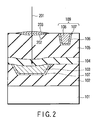
- FIG. 2 is a cross-sectional view for explaining the judgment of the residue of the metal film in forming the Cu damascene wiring in Example 1 of the present invention
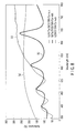
- FIGS. 3A to 3 C are graphs each showing the reflectance spectrum that is changed with progress of the CMP treatment in Example 1 of the present invention
- FIG. 4 is a flow chart for judging the residue of the metal film in the CMP treatment
- FIG. 5 schematically shows the construction of an apparatus for measuring the residue of the metal film in the CMP treatment
- FIGS. 6A to 6 C collectively show the construction of an in-situ reflectance measuring apparatus for measuring the reflectance during the CMP treatment applied to a Cu film in Example 2 of the present invention
- FIGS. 7A to 7 C are cross-sectional views for explaining the judgment on the residue of the metal film in forming an aluminum pad above a Cu damascene wiring in Example 3 of the present invention.
- FIG. 8 is a graph showing the reflectance spectrum that is changed with progress in the RIE treatment in forming an Al pad in Example 3 of the present invention.
- the method of judging the residual film by an optical measurement comprises measuring the change in the intensity of light reflected from a sample depending on the wavelength of the measuring light so as to obtain a reflectance spectrum curve, and dividing the reflectance spectrum curve into a plurality of wavelength regions so as to judge presence or absence of a second metal film on an insulating film formed on a first metal film depending on the waveform of the reflectance spectrum curve in each of the wavelength regions.
- the presence or absence of the second metal film on the insulating film is judged by only the amplitude of the reflectance spectrum curve divided depending on the wavelength of light reflected from the sample, with the result that the polishing residual film can be judged easily and in a short time while eliminating the necessity in the prior art for measuring the thickness of the residual film.
- the presence or absence of the second metal film on the insulating film is judged by allowing the presence or absence of the periodic wave, or the amplitude of the periodic wave in each of the wavelength regions of the reflectance spectrum curve to correspond to the presence or absence of the second metal film on the insulating film.
- the first metal it is desirable for the first metal to be a metal whose reflectance is rapidly changed depending on the wavelength of the measuring light.
- the first metal layer it is desirable for the first metal layer to be thick enough to prevent the measuring light from being transmitted therethrough.
- the thickness of the first metal layer may be at least about 100 nm.
- a Cu wiring to constitute the first metal film and for a metal film forming an underlying barrier film to constitute the second metal film. It is possible for the judging method according to the first embodiment of the present invention to be employed for the judgment on the presence or absence of these barrier film and metal film on an insulating film.
- the reflectance spectrum curve is divided into a plurality of regions including a region on the side of a short wavelength not longer than 500 nm and a region on the side of a long wavelength not shorter than 650 nm. It is possible to judge any of the three states including (a) the presence of a thick metal film, (b) the presence of a thin metal film and a barrier film, or the absence of a metal film and the presence of a barrier film, and (c) the absence of a metal film and a barrier film, by allowing the presence or absence, or the amplitude of the periodic wave on the side of the short wavelength and on the side of the long wavelength in the reflectance spectrum curve to correspond to the three states (a) to (c) noted above.
- the residual film can be judged based on only two wavelength regions of the reflectance spectrum curve so as to make it possible to judge the residual film easily and in a short time.
- the insulating film in the method according to the first embodiment of the present invention, it is possible for the insulating film to be a film selected from the group consisting of a silicon oxide film, a silicon nitride film, a silicon oxide film to which at least one of fluorine, phosphorus and boron is added, an organic insulating film, and a laminated film including some of these insulating films. It is desirable for the insulating film to be formed of a material low in absorption of light having a wavelength falling within a range of the wavelengths of the measuring light components and substantially transparent to light and to have a thickness large enough to generate interference accompanying the wavelength. For example, it is desirable for the insulating film to have a thickness of 0.2 to 2 ⁇ m.
- the barrier film is a film selected from the group consisting of a tantalum film, a tantalum nitride film, a titanium film, a titanium nitride film, a tungsten film, a tungsten nitride film, and a laminated film including some of these barrier films. It is desirable for the barrier film to have a thickness that permits transmitting light having a wavelength range of the measuring light. For example, it is desirable for the barrier film to have a thickness of 50 nm or less.
- the method of judging the residual film by an optical measurement is applied to the manufacturing method of a semiconductor device utilizing the detection of the end point of the removal of the second metal film.
- the second metal film can be removed by, for example, a CMP (Chemical Mechanical Polishing) method or a RIE (Reactive Ion Etching) method.
- CMP Chemical Mechanical Polishing
- RIE Reactive Ion Etching
- the method of judging the residual film by an optical measurement can be effectively utilized for detecting the end point of the CMP treatment in the case where a metal film is buried using the CMP treatment in at least one of a groove and a hole formed in an insulating film.
- an insulating film 102 is formed on the surface of a semiconductor substrate 101 having active elements (not shown) formed therein. Also, a Cu buried wiring 103 is formed in the insulating film 102 with a tantalum nitride (TaN) liner film 107 interposed between the Cu buried wiring 103 and the insulating film 102 . Further, a silicon nitride (SiN) film 104 and a silicon dioxide (SiO 2 ) film 105 acting as an interlayer insulating film are successively formed on the resultant structure.
- TiN silicon nitride
- SiO 2 silicon dioxide
- a wiring groove 106 and a hole (not shown) for forming a plug serving to connect electrically the lower wiring layer to the upper wiring layer are formed in the interlayer insulating film 105 , following by forming a laminate structure of a tantalum nitride (TaN) liner film 107 and a copper (Cu) film 108 in a manner to fill the wiring groove 106 .
- TaN tantalum nitride
- Cu copper
- those regions of the copper (Cu) film 108 and the tantalum nitride (TaN) liner film 107 which are positioned on the field portion (outside the wiring groove 106 ) are removed by the CMP (Chemical Mechanical Polishing) method so as to permit the films 108 and 107 to remain unremoved within the wiring groove 106 , thereby forming a Cu buried wiring 109 , as shown in FIGS. 1B and 1C.
- CMP Chemical Mechanical Polishing
- FIG. 2 shows how the field portion of the interlayer insulating film 105 is irradiated with light 201 during the CMP treatment so as to measure the reflectance.
- the reflectance is measured by changing the wavelength within a range of between 300 nm and 800 nm.
- a large dishing is formed on the Cu wiring 103 having a large width of scores of microns, to which an optical measurement can be applied, and a residual film 202 of the TaN film 107 and a residual film 203 of the Cu film 108 tend to be generated above the dished portion. Therefore, the region above the Cu wiring 103 is adapted for monitoring the residual film after the CMP treatment.
- the reflectance spectrum is changed in accordance with progress of the CMP treatment as shown in FIGS. 3A to 3 C.
- the reflectance shown in each of FIGS. 3A to 3 C is on the basis that the reflectance of the silicon (Si) substrate is set at 100%.
- Stage (a) shows the state that the Cu film 108 on the interlayer insulating film 105 shown in FIG. 1A is so thick that the measuring light is incapable of being transmitted therethrough. In this case, a reflectance similar to that of the Cu bulk is exhibited under the measuring wavelength region, as shown in FIG. 3A. The periodic amplitude cannot be recognized under the wavelength not longer than 500 nm and under the wavelength not shorter than 650 nm.
- Stage (b) shows the state that the Cu film 108 is thin enough to permit the measuring light to be transmitted therethrough, or the Cu film 108 is removed.
- the Cu film 108 is substantially removed and the TaN film 107 is left unremoved.
- the amplitude is present over the entire measuring wavelength region, as shown in FIG. 3B.
- stage (c) shows the state that both the Cu film 108 and the TaN film 107 are removed.
- the amplitude can be recognized under the wavelength not longer than 500 nm but cannot be recognized under the wavelength not shorter than 650 nm, as shown in FIG. 3C.
- the presence or absence of the periodic wave on the long wavelength side is judged first. Where there is a periodic wave, it is judged that there is no residual Cu film and there is a residual BM film. Where a periodic wave is not recognized on the long wavelength side, the presence or absence of the periodic wave on the short wavelength side is judged. Where a periodic wave is recognized on the short wavelength side, it is judged that there is no residual Cu film and no residual BM film. Further, where a periodic wave is not recognized on the short wavelength side, it is judged that there are a residual Cu film and a residual BM film.
- FIG. 5 schematically shows the construction of an apparatus for judging the residual film after the CMP treatment by the method described above.
- the residual film after the CMP treatment is rendered nonuniform by, for example, the pattern density or the step of the underlying layer.
- a measuring point such as point (a) shown in FIG. 5
- the film thickness is calculated by the procedure that the spectrum obtained by the calculation, in which the thickness of each layer is changed, is allowed to fit the measured spectrum, and the film thickness value in the case where the spectrum obtained by the calculation is closest to the measured spectrum is employed for judging the residual metal film. It follows that the calculating time is increased with increase in the number of kinds of the films whose thicknesses are obtained and in the range of calculation of the film thickness. Such being the situation, it takes a very long time to calculate the film thickness at a plurality of points by the conventional method of judging the residual film.
- Example 1 In the method of judging the residual film in Example 1, however, it suffices to make the judgment based on at least two criteria including the presence or absence of the periodic wave on the long wavelength side and the short wavelength side in the reflectance curve so as to make it possible to eliminate the voluminous calculation required in the conventional method. It should also be noted that, since the determination of an accurate film thickness value is not required for performing the inspection alone of the residual film, the method in Example 1 of the present invention is highly effective in the case of polishing a large region like the CMP treatment, i.e., in judging the residual film in many measuring points.
- Example 2 is directed to an example of measuring in-situ the reflectance during the CMP treatment applied to the Cu film included in the wafer equal in construction to the wafer used in Example 1, i.e., the wafer constructed such that a plurality of films are laminated on a semiconductor substrate.
- FIG. 6A is an oblique view showing the construction of the CMP apparatus
- FIG. 6B is a plan view of the CMP apparatus shown in FIG. 6A
- FIG. 6C is a side cross-sectional view showing the left side portion of the CMP apparatus shown in FIG. 6A.
- the CMP apparatus is constructed as follows. Specifically, a polishing pad 603 is arranged on a turntable 601 , and a wafer 605 supported by a carrier 607 is arranged such that the surface of the wafer 605 that is to be polished faces downward. A slurry supply nozzle 609 is arranged above the polishing pad 603 such that the wafer 605 is polished by a polishing slurry 606 supplied from the slurry supply nozzle 609 .
- the wafer 605 is irradiated with a measuring light 608 , and light reflected from the wafer 605 passes through an optical window 604 formed in the polishing pad 603 so as to be detected by an optical head 602 arranged in a hollow space formed in the turntable 601 , thereby measuring the reflectance.
- the amplitude of the periodic wave in the reflectance curve relative to the wavelength is made small or the periodic wave is eliminated at the short wavelength not longer than 500 nm and at the long wavelength not shorter than 650 nm as shown in FIG. 3A in conjunction with Example 1, though there is an influence of the scattering by, for example, the polishing slurry 606 .
- This Example is directed to the formation of an aluminum pad on a copper (Cu) damascene wiring, as shown in FIGS. 7A to 7 C.
- a copper (Cu) buried wiring 703 is formed in an insulating film 702 on a semiconductor substrate 701 having an active element (not shown) formed therein.
- a tantalum nitride (TaN) liner film 700 is interposed between the copper buried wiring 703 and the insulating film 702 .
- a silicon nitride (SiN) film 704 and a silicon dioxide (SiO 2 ) film 705 constituting an interlayer insulating film are successively formed on the resultant structure, followed by patterning the interlayer insulating film 705 so as to form an opening 706 .
- a tantalum (Ta) film 707 as a barrier metal layer and an aluminum (Al) film 708 are formed on the interlayer insulating film 705 in a manner to fill the opening 706 .
- a resist film is formed on the entire surface, followed by patterning the resist film such that a resist 709 is left in the portion forming an Al pad, as shown in FIG. 7A.
- stage (c) in which the Al film 708 and the Ta film 707 are eliminated as shown in FIG. 7C, is reached through stage (a), in which the Al film 708 is left unremoved as shown in FIG. 7A, and stage (b), in which the Al film 708 is eliminated and the Ta film 707 is left unremoved as shown in FIG. 7B.
- stage (c) in which the Al film 708 and the Ta film 707 are eliminated as shown in FIG. 7C
- stage (b) in which the Al film 708 is eliminated and the Ta film 707 is left unremoved as shown in FIG. 7B.
- the interlayer insulating film 705 above the lower layer Cu wiring 703 was irradiated with light 800 so as to measure the reflectance by changing the wavelength within a range of between 350 nm and 800 nm.
- three reflectance spectra as shown in FIG. 8 were obtained in accordance with progress of the RIE treatment.
- the reflectance spectra (a), (b) and (c) shown in FIG. 8 correspond to the stages (a), (b) and (c) referred to above, respectively.
- the reflectance shown in FIG. 8 is on the basis that the reflectance of the Si substrate is set at 100%.
- Stage (a) denotes the state that the Al film 708 is present in a large thickness on the interlayer insulating film 705 and exhibits a reflectance similar to that of an Al bulk in the measuring wavelength region. It is impossible to recognize a periodic wave on the short wavelength side and on the long wavelength side.
- Stage (b) denotes the state that the Al film 708 is removed substantially completely and the Ta film 707 is left unremoved. In this case, an amplitude is present over the entire measuring wavelength region.
- stage (c) denotes the state that both the Al film 708 and the Ta film 707 are removed substantially completely.
- a periodic wave can be recognized in the wavelength region not longer than 500 nm.
- a periodic wave is not recognized in a wavelength region not shorter than 650 nm.
- the residue of the Al film and the barrier metal film can be judged easily in Example 3, too, by application of the flow chart shown in FIG. 4 and Table 1 directed to a judgment table based on the presence or absence of the periodic wave in the reflectance spectrum curve as in Example 1.
- a method of judging the residual film by an optical measurement produces various merits that the complicated calculation of the optical model is made unnecessary, that a precise optical measurement is made unnecessary, that the judging time can be shortened, and that the judgment of the residual metal film in many points can be performed on the real time basis.
Abstract
Description
- This application is based upon and claims the benefit of priority from the prior Japanese Patent Application No. 2002-089775, filed Mar. 27, 2002, the entire contents of which are incorporated herein by reference.
- 1. Field of the Invention
- The present invention relates to a method of judging a residual film by an optical measurement, particularly, to a method of judging a residual film by means of a spectral reflection interferometer in the inspecting step involved in the manufacturing process of a semiconductor device.
- 2. Description of the Related Art
- In the conventional method of measuring a film thickness by using a spectral reflection interferometer, fitting is performed between the measured reflectance spectrum and the reflection spectrum calculated from an expected model of a stacked film so as to determine the film thickness, thereby judging the laminate structure of a sample. In the conventional method, however, the fitting becomes poor if the structure of the film to be measured differs from that of the optical model used for the film thickness calculation, with the result that it is possible for the judgment to be erroneous.
- In CMP of a Cu film, which is carried out for forming a Cu damascene wiring over a Cu buried wiring with an interlayer insulating film interposed therebetween, a Cu film and a barrier metal (BM) film are polished so as to remove completely the Cu film and the barrier metal (BM) film in a field portion other than the wiring section while allowing the Cu film and the barrier metal (BM) film to be left unremoved in the wiring section alone. Therefore, under the state that the Cu film is left unremoved, the residual film in the field portion has a stacked structure of a Cu film/BM film/interlayer insulating film/Cu buried wiring. It follows that it is necessary to carry out the film thickness calculation while changing the thickness of each of at least the Cu film, the BM film and the interlayer insulating film, leading to the requirement of a tremendous calculation amount.
- Such being the situation, it is conceivable to decrease the calculation amount by dividing the situation into several cases as follows depending on the CMP treatment.
- Specifically, the state of the field portion can be classified into at least the three states given below:
- a) Presence of a Cu residual film (NG—additional polishing);
- b) Presence of a BM residual film (NG—additional polishing);
- c) No residual film (finish OK)
- It is conceivable to classify the state of the field portion into the three states given above and to carry out the film thickness calculation while changing the thickness of each of the uppermost layer and the layer immediately below the uppermost layer. In this method, however, it is necessary to carry out the film thickness calculation by assuming the construction of each of the layers, and it is difficult to classify the state into suitable cases. Under the circumstances, a simpler method is required for judging the residual film in the field portion.
- According to an aspect of the present invention, there is provided a method of judging a residual film on a sample by an optical measurement, the sample including a first metal film whose reflectance is changed depending on a wavelength of measuring light, and an insulating film formed above the first metal film, and the residual film being a second metal film above the insulating film, the method comprising: irradiating the sample with a measuring light so as to measure a change in intensity of light reflected from the sample depending on the wavelength of the measuring light, thereby obtaining a reflectance spectrum curve; and dividing the reflectance spectrum curve into a plurality of wavelength regions so as to judge presence or absence of the second metal film above the insulating film depending on a waveform in each of the wavelength regions of the reflectance spectrum curve.
- According to another aspect of the present invention, there is provided a method of judging a residual film by an optical measurement for judging presence or absence of a barrier film and a metal film above an insulating film of a semiconductor substrate provided with a Cu wiring and the insulating film formed above the Cu wiring, comprising: irradiating a surface of the semiconductor substrate above the Cu wiring with a measuring light so as to measure a change in intensity of light reflected from the semiconductor substrate depending on a wavelength of the measuring light, thereby obtaining a reflectance spectrum curve; and dividing the reflectance spectrum curve into a plurality of regions including a wavelength region on a side of a short wavelength not longer than 500 nm and a wavelength region on a side of a long wavelength not shorter than 650 nm so as to judge any of three states on the insulating film including (a) substantially presence of the metal film, (b) substantially absence of the metal film and presence of the barrier film, and (c) absence of the metal film and absence of the barrier film, by allowing presence or absence of a periodic wave, or amplitude of the periodic wave on the side of each of the short wavelength and the long wavelength in the reflectance spectrum curve to correspond to the three states given above.
- Further, according to still another aspect of the present invention, there is provided a method of manufacturing a semiconductor device, comprising: providing a semiconductor substrate including a first metal film whose reflectance is changed depending on the wavelength of a measuring light and an insulating film formed above the first metal film; depositing a second metal film above the insulating film; removing selectively the second metal film from a surface of the second metal film gradually; irradiating a prescribed region of the semiconductor substrate with a measuring light so as to measure a change in intensity of light reflected from the semiconductor substrate depending on the wavelength of the measuring light, thereby obtaining a reflectance spectrum curve; and dividing the reflectance spectrum curve into a plurality of wavelength regions so as to judge presence or absence of the second metal film above the insulating film in a prescribed region depending on waveform of the reflectance spectrum curve in each of wavelength regions, thereby detecting an end point in removal of the second metal film, wherein the removal of the second metal film is stopped based on the detected end point so as to finish removing the second metal film.
- FIGS. 1A to 1C are cross-sectional views collectively showing the process of forming a Cu damascene wiring in Example 1 of the present invention;
- FIG. 2 is a cross-sectional view for explaining the judgment of the residue of the metal film in forming the Cu damascene wiring in Example 1 of the present invention;
- FIGS. 3A to 3C are graphs each showing the reflectance spectrum that is changed with progress of the CMP treatment in Example 1 of the present invention;
- FIG. 4 is a flow chart for judging the residue of the metal film in the CMP treatment;
- FIG. 5 schematically shows the construction of an apparatus for measuring the residue of the metal film in the CMP treatment;
- FIGS. 6A to 6C collectively show the construction of an in-situ reflectance measuring apparatus for measuring the reflectance during the CMP treatment applied to a Cu film in Example 2 of the present invention;
- FIGS. 7A to 7C are cross-sectional views for explaining the judgment on the residue of the metal film in forming an aluminum pad above a Cu damascene wiring in Example 3 of the present invention; and
- FIG. 8 is a graph showing the reflectance spectrum that is changed with progress in the RIE treatment in forming an Al pad in Example 3 of the present invention.
- Some embodiments of the present invention will now be described.
- As a result of extensive research conducted on the method of judging by an optical measurement the residual film in the polishing step, the present inventors paid attention to the situation that, since the polishing is insufficient in the case where the polishing residual film is present in the field portion, judgment on only the presence or absence of the polishing residual film is required for the judgment on the necessity of, for example, additional polishing, and the thickness of the polishing residual film in the field portion is not necessarily required information.
- The method of judging the residual film by an optical measurement according to a first embodiment of the present invention, which is based on the particular situation described above, comprises measuring the change in the intensity of light reflected from a sample depending on the wavelength of the measuring light so as to obtain a reflectance spectrum curve, and dividing the reflectance spectrum curve into a plurality of wavelength regions so as to judge presence or absence of a second metal film on an insulating film formed on a first metal film depending on the waveform of the reflectance spectrum curve in each of the wavelength regions.
- In the method according to the first embodiment of the present invention, the presence or absence of the second metal film on the insulating film is judged by only the amplitude of the reflectance spectrum curve divided depending on the wavelength of light reflected from the sample, with the result that the polishing residual film can be judged easily and in a short time while eliminating the necessity in the prior art for measuring the thickness of the residual film.
- To be more specific, in the method of judging the residual film according to the first embodiment of the present invention, the presence or absence of the second metal film on the insulating film is judged by allowing the presence or absence of the periodic wave, or the amplitude of the periodic wave in each of the wavelength regions of the reflectance spectrum curve to correspond to the presence or absence of the second metal film on the insulating film.
- In this case, it is desirable for the first metal to be a metal whose reflectance is rapidly changed depending on the wavelength of the measuring light. To be more specific, it is desirable for the first metal to be a colored metal such as Cu or Au. It is desirable for the first metal layer to be thick enough to prevent the measuring light from being transmitted therethrough. For example, the thickness of the first metal layer may be at least about 100 nm.
- Also, in the method of judging the residual film by an optical measurement according to the first embodiment of the present invention, it is possible for a Cu wiring to constitute the first metal film and for a metal film forming an underlying barrier film to constitute the second metal film. It is possible for the judging method according to the first embodiment of the present invention to be employed for the judgment on the presence or absence of these barrier film and metal film on an insulating film.
- In this case, the reflectance spectrum curve is divided into a plurality of regions including a region on the side of a short wavelength not longer than 500 nm and a region on the side of a long wavelength not shorter than 650 nm. It is possible to judge any of the three states including (a) the presence of a thick metal film, (b) the presence of a thin metal film and a barrier film, or the absence of a metal film and the presence of a barrier film, and (c) the absence of a metal film and a barrier film, by allowing the presence or absence, or the amplitude of the periodic wave on the side of the short wavelength and on the side of the long wavelength in the reflectance spectrum curve to correspond to the three states (a) to (c) noted above.
- To be more specific, where the periodic wave on any of the short wavelength side and the long wavelength side in the reflectance spectrum curve is not present or the amplitude of that periodic wave is small, it is judged that the situation on the insulating film is under state (a) given above. Where the periodic wave on each of the short wavelength side and the long wavelength side in the reflectance spectrum curve is present or the amplitude of that periodic wave is large, it is judged that the situation on the insulating film is under state (b) given above. Further, where the periodic wave on the short wavelength side in the reflectance spectrum curve is present or the amplitude of that periodic wave is large, and the periodic wave on the long wavelength side in the reflectance spectrum curve is not present or the amplitude of that periodic wave is small, it is judged that the situation on the insulating film is under state (c) given above.
- As described above, the residual film can be judged based on only two wavelength regions of the reflectance spectrum curve so as to make it possible to judge the residual film easily and in a short time.
- In the method according to the first embodiment of the present invention, it is possible for the insulating film to be a film selected from the group consisting of a silicon oxide film, a silicon nitride film, a silicon oxide film to which at least one of fluorine, phosphorus and boron is added, an organic insulating film, and a laminated film including some of these insulating films. It is desirable for the insulating film to be formed of a material low in absorption of light having a wavelength falling within a range of the wavelengths of the measuring light components and substantially transparent to light and to have a thickness large enough to generate interference accompanying the wavelength. For example, it is desirable for the insulating film to have a thickness of 0.2 to 2 μm.
- On the other hand, it is possible for the barrier film to be a film selected from the group consisting of a tantalum film, a tantalum nitride film, a titanium film, a titanium nitride film, a tungsten film, a tungsten nitride film, and a laminated film including some of these barrier films. It is desirable for the barrier film to have a thickness that permits transmitting light having a wavelength range of the measuring light. For example, it is desirable for the barrier film to have a thickness of 50 nm or less.
- In another embodiment of the present invention, the method of judging the residual film by an optical measurement is applied to the manufacturing method of a semiconductor device utilizing the detection of the end point of the removal of the second metal film.
- The second metal film can be removed by, for example, a CMP (Chemical Mechanical Polishing) method or a RIE (Reactive Ion Etching) method. Particularly, the method of judging the residual film by an optical measurement can be effectively utilized for detecting the end point of the CMP treatment in the case where a metal film is buried using the CMP treatment in at least one of a groove and a hole formed in an insulating film.
- To be more specific, it is possible to detect the end point of the polishing easily and in a short time in depositing a second metal film in a manner to fill at least one of a groove and a hole made in an insulating film, followed by polishing the deposited second metal film so as to permit the residual second metal film to be buried in at least one of the groove and the hole while removing that portion of the deposited second metal film which is positioned on the insulating film on the outside of the groove and the hole.
- Various Examples of the present invention will now be described with reference to the accompanying drawings.
- The formation of a laminate structure of a Cu damascene wiring will now be described with reference to FIG. 1. As shown in FIG. 1A, an insulating
film 102 is formed on the surface of asemiconductor substrate 101 having active elements (not shown) formed therein. Also, a Cu buriedwiring 103 is formed in the insulatingfilm 102 with a tantalum nitride (TaN)liner film 107 interposed between the Cu buriedwiring 103 and the insulatingfilm 102. Further, a silicon nitride (SiN)film 104 and a silicon dioxide (SiO2)film 105 acting as an interlayer insulating film are successively formed on the resultant structure. - In the next step, a
wiring groove 106 and a hole (not shown) for forming a plug serving to connect electrically the lower wiring layer to the upper wiring layer are formed in theinterlayer insulating film 105, following by forming a laminate structure of a tantalum nitride (TaN)liner film 107 and a copper (Cu)film 108 in a manner to fill thewiring groove 106. After formation of the laminate structure noted above, those regions of the copper (Cu)film 108 and the tantalum nitride (TaN)liner film 107 which are positioned on the field portion (outside the wiring groove 106) are removed by the CMP (Chemical Mechanical Polishing) method so as to permit thefilms wiring groove 106, thereby forming a Cu buriedwiring 109, as shown in FIGS. 1B and 1C. - In this case, the situation above the field portion of the
interlayer insulating film 105 is changed in three stages given below in accordance with the progress of the polishing by the CMP treatment: - a) The stage in which the
Cu film 108 remains substantially unremoved; - b) The stage in which the
Cu film 108 is substantially eliminated and theTaN film 107 remains unremoved; - c) The stage in which both the
Cu film 108 and theTaN film 107 are eliminated. - FIG. 2 shows how the field portion of the
interlayer insulating film 105 is irradiated with light 201 during the CMP treatment so as to measure the reflectance. The reflectance is measured by changing the wavelength within a range of between 300 nm and 800 nm. Incidentally, a large dishing is formed on theCu wiring 103 having a large width of scores of microns, to which an optical measurement can be applied, and aresidual film 202 of theTaN film 107 and aresidual film 203 of theCu film 108 tend to be generated above the dished portion. Therefore, the region above theCu wiring 103 is adapted for monitoring the residual film after the CMP treatment. - The reflectance spectrum is changed in accordance with progress of the CMP treatment as shown in FIGS. 3A to 3C. Incidentally, the reflectance shown in each of FIGS. 3A to 3C is on the basis that the reflectance of the silicon (Si) substrate is set at 100%.
- Stage (a) shows the state that the
Cu film 108 on theinterlayer insulating film 105 shown in FIG. 1A is so thick that the measuring light is incapable of being transmitted therethrough. In this case, a reflectance similar to that of the Cu bulk is exhibited under the measuring wavelength region, as shown in FIG. 3A. The periodic amplitude cannot be recognized under the wavelength not longer than 500 nm and under the wavelength not shorter than 650 nm. - Stage (b) shows the state that the
Cu film 108 is thin enough to permit the measuring light to be transmitted therethrough, or theCu film 108 is removed. In other words, theCu film 108 is substantially removed and theTaN film 107 is left unremoved. In this case, the amplitude is present over the entire measuring wavelength region, as shown in FIG. 3B. - Further, stage (c) shows the state that both the
Cu film 108 and theTaN film 107 are removed. In this case, the amplitude can be recognized under the wavelength not longer than 500 nm but cannot be recognized under the wavelength not shorter than 650 nm, as shown in FIG. 3C. - In conclusion, the judgment can be made as shown in Table 1 below:
TABLE 1 Short Long wavelength wavelength side side (≦500 nm) (≧650 nm) Residual Residual periodic wave periodic wave Cu film BM film none none recognized recognized recognized recognized none recognized recognized none none none - It should be noted that it is reasonable to judge that, where a periodic wave is not recognized in any of the short wavelength side having a wavelength not longer than 500 nm and the long wavelength side having a wavelength not shorter than 650 nm, both the residual Cu film and the residual BM film are present. Also, where a periodic wave is recognized in each of the short wavelength side having a wavelength not longer than 500 nm and the long wavelength side having a wavelength not shorter than 650 nm, it is reasonable to judge that the residual Cu film is substantially eliminated and the residual BM film is present. Further, where a periodic wave is recognized in the short wavelength side having a wavelength not longer than 500 nm and is not recognized in the long wavelength side having a wavelength not shorter than 650 nm, it is reasonable to judge that both the residual Cu film and the residual BM film are eliminated.
- In this case, it is possible to make a judgment in accordance with the flow chart shown in FIG. 4. Specifically, the presence or absence of the periodic wave on the long wavelength side is judged first. Where there is a periodic wave, it is judged that there is no residual Cu film and there is a residual BM film. Where a periodic wave is not recognized on the long wavelength side, the presence or absence of the periodic wave on the short wavelength side is judged. Where a periodic wave is recognized on the short wavelength side, it is judged that there is no residual Cu film and no residual BM film. Further, where a periodic wave is not recognized on the short wavelength side, it is judged that there are a residual Cu film and a residual BM film.
- As described above, it is possible to judge easily the residual Cu film and the residual barrier metal film by using as a criterion of the judgment the periodic wave in a curve obtained by plotting the change in the reflectance relative to the wavelength in the wavelength region on the long wavelength side and the short wavelength side.
- FIG. 5 schematically shows the construction of an apparatus for judging the residual film after the CMP treatment by the method described above. There is a case where the residual film after the CMP treatment is rendered nonuniform by, for example, the pattern density or the step of the underlying layer. Where there is no Cu residual film and no TaN residual film at a measuring point such as point (a) shown in FIG. 5, it is possible for the residual film to be overlooked. In order to suppress the overlooking of the residual film, it is desirable to carry out the measurement at a plurality of points.
- It was customary in the past to judge the residual metal film by obtaining the thickness value of each layer. The film thickness is calculated by the procedure that the spectrum obtained by the calculation, in which the thickness of each layer is changed, is allowed to fit the measured spectrum, and the film thickness value in the case where the spectrum obtained by the calculation is closest to the measured spectrum is employed for judging the residual metal film. It follows that the calculating time is increased with increase in the number of kinds of the films whose thicknesses are obtained and in the range of calculation of the film thickness. Such being the situation, it takes a very long time to calculate the film thickness at a plurality of points by the conventional method of judging the residual film. In the method of judging the residual film in Example 1, however, it suffices to make the judgment based on at least two criteria including the presence or absence of the periodic wave on the long wavelength side and the short wavelength side in the reflectance curve so as to make it possible to eliminate the voluminous calculation required in the conventional method. It should also be noted that, since the determination of an accurate film thickness value is not required for performing the inspection alone of the residual film, the method in Example 1 of the present invention is highly effective in the case of polishing a large region like the CMP treatment, i.e., in judging the residual film in many measuring points.
- The embodiment for Example 2 is directed to an example of measuring in-situ the reflectance during the CMP treatment applied to the Cu film included in the wafer equal in construction to the wafer used in Example 1, i.e., the wafer constructed such that a plurality of films are laminated on a semiconductor substrate.
- A CMP apparatus constructed as shown in FIGS. 6A to 6C is used for this method. Specifically, FIG. 6A is an oblique view showing the construction of the CMP apparatus, FIG. 6B is a plan view of the CMP apparatus shown in FIG. 6A, and FIG. 6C is a side cross-sectional view showing the left side portion of the CMP apparatus shown in FIG. 6A.
- The CMP apparatus is constructed as follows. Specifically, a
polishing pad 603 is arranged on aturntable 601, and awafer 605 supported by acarrier 607 is arranged such that the surface of thewafer 605 that is to be polished faces downward. Aslurry supply nozzle 609 is arranged above thepolishing pad 603 such that thewafer 605 is polished by a polishingslurry 606 supplied from theslurry supply nozzle 609. During the polishing treatment, thewafer 605 is irradiated with a measuring light 608, and light reflected from thewafer 605 passes through anoptical window 604 formed in thepolishing pad 603 so as to be detected by anoptical head 602 arranged in a hollow space formed in theturntable 601, thereby measuring the reflectance. - In this method, it is impossible to perform the measurement at a specified site of a prescribed structure on a patterned wafer, and an averaged intensity of the reflected light from the part of the wafer passing over the
optical head 602 during the measuring time is obtained as the output. However, in the initial stage of the CMP treatment applied to the Cu film, not only the buried wiring portion but also the field portion are covered with the Cu film. It follows that the entire wafer surface exhibits a reflectance similar to that of a Cu bulk, though there is a slight change in the reflectance caused by the step. Under the circumstances, where the Cu film covers the entire surface of thewafer 605 in the initial stage of the polishing applied to the Cu film, the amplitude of the periodic wave in the reflectance curve relative to the wavelength is made small or the periodic wave is eliminated at the short wavelength not longer than 500 nm and at the long wavelength not shorter than 650 nm as shown in FIG. 3A in conjunction with Example 1, though there is an influence of the scattering by, for example, the polishingslurry 606. - However, if the Cu film in the field portion comes to be eliminated, a periodic wave begins to be observed in the reflectance curve. Although a clear change in the spectrum does not appear, compared with the case of measuring the reflectance on the Cu wiring alone as in Example 1, it is possible to judge depending on the amplitude of the periodic wave in two wavelength regions of the reflectance curve that a Cu film or a barrier metal film is present on the entire surface. Therefore, it is possible to utilize the method of Example 2 for detecting the end point of the polishing.
- This Example is directed to the formation of an aluminum pad on a copper (Cu) damascene wiring, as shown in FIGS. 7A to 7C. As shown in the drawings, a copper (Cu) buried
wiring 703 is formed in an insulatingfilm 702 on asemiconductor substrate 701 having an active element (not shown) formed therein. Also, a tantalum nitride (TaN)liner film 700 is interposed between the copper buriedwiring 703 and the insulatingfilm 702. Further, a silicon nitride (SiN)film 704 and a silicon dioxide (SiO2)film 705 constituting an interlayer insulating film are successively formed on the resultant structure, followed by patterning theinterlayer insulating film 705 so as to form anopening 706. - In the next step, a tantalum (Ta)
film 707 as a barrier metal layer and an aluminum (Al)film 708 are formed on theinterlayer insulating film 705 in a manner to fill theopening 706. Then, a resist film is formed on the entire surface, followed by patterning the resist film such that a resist 709 is left in the portion forming an Al pad, as shown in FIG. 7A. - After patterning the resist film, the
Al film 708 and theTa film 707 are selectively removed by a RIE (Reactive Ion Etching) method with the resist 709 used as a mask. In accordance with progress of the RIE treatment, stage (c), in which theAl film 708 and theTa film 707 are eliminated as shown in FIG. 7C, is reached through stage (a), in which theAl film 708 is left unremoved as shown in FIG. 7A, and stage (b), in which theAl film 708 is eliminated and theTa film 707 is left unremoved as shown in FIG. 7B. - The
interlayer insulating film 705 above the lowerlayer Cu wiring 703 was irradiated with light 800 so as to measure the reflectance by changing the wavelength within a range of between 350 nm and 800 nm. As a result, three reflectance spectra as shown in FIG. 8 were obtained in accordance with progress of the RIE treatment. It should be noted that the reflectance spectra (a), (b) and (c) shown in FIG. 8 correspond to the stages (a), (b) and (c) referred to above, respectively. Incidentally, the reflectance shown in FIG. 8 is on the basis that the reflectance of the Si substrate is set at 100%. - Stage (a) denotes the state that the
Al film 708 is present in a large thickness on theinterlayer insulating film 705 and exhibits a reflectance similar to that of an Al bulk in the measuring wavelength region. It is impossible to recognize a periodic wave on the short wavelength side and on the long wavelength side. - Stage (b) denotes the state that the
Al film 708 is removed substantially completely and theTa film 707 is left unremoved. In this case, an amplitude is present over the entire measuring wavelength region. - Further, stage (c) denotes the state that both the
Al film 708 and theTa film 707 are removed substantially completely. In this case, a periodic wave can be recognized in the wavelength region not longer than 500 nm. However, a periodic wave is not recognized in a wavelength region not shorter than 650 nm. - As described above, the residue of the Al film and the barrier metal film can be judged easily in Example 3, too, by application of the flow chart shown in FIG. 4 and Table 1 directed to a judgment table based on the presence or absence of the periodic wave in the reflectance spectrum curve as in Example 1.
- As described above in detail, according to embodiments of the present invention, provided is a method of judging the residual film by an optical measurement. The method provided by the embodiments of the present invention produces various merits that the complicated calculation of the optical model is made unnecessary, that a precise optical measurement is made unnecessary, that the judging time can be shortened, and that the judgment of the residual metal film in many points can be performed on the real time basis.
- Additional advantages and modifications will readily occur to those skilled in the art. Therefore, the present invention in its broader aspects is not limited to the specific details and representative embodiments shown and described herein. Accordingly, various modifications may be made without departing from the spirit or scope of the general inventive concept as defined by the appended claims and their equivalents.
Claims (20)
Applications Claiming Priority (2)
| Application Number | Priority Date | Filing Date | Title |
|---|---|---|---|
| JP2002-089775 | 2002-03-27 | ||
| JP2002089775A JP3779636B2 (en) | 2002-03-27 | 2002-03-27 | Determination method of residual film by optical measurement |
Publications (2)
| Publication Number | Publication Date |
|---|---|
| US20030197859A1 true US20030197859A1 (en) | 2003-10-23 |
| US6984532B2 US6984532B2 (en) | 2006-01-10 |
Family
ID=28449537
Family Applications (1)
| Application Number | Title | Priority Date | Filing Date |
|---|---|---|---|
| US10/396,310 Expired - Fee Related US6984532B2 (en) | 2002-03-27 | 2003-03-26 | Method of judging residual film by optical measurement |
Country Status (5)
| Country | Link |
|---|---|
| US (1) | US6984532B2 (en) |
| JP (1) | JP3779636B2 (en) |
| KR (1) | KR100502120B1 (en) |
| CN (1) | CN100407392C (en) |
| TW (1) | TWI223366B (en) |
Cited By (5)
| Publication number | Priority date | Publication date | Assignee | Title |
|---|---|---|---|---|
| US20060071208A1 (en) * | 2004-10-04 | 2006-04-06 | International Business Machines Corporation | Inspection methods and structures for visualizing and/or detecting specific chip structures |
| US20080130000A1 (en) * | 2006-12-05 | 2008-06-05 | Applied Materials, Inc. | Determining copper concentration in spectra |
| US20110275167A1 (en) * | 2010-05-05 | 2011-11-10 | Jeffrey Drue David | Endpoint Method Using Peak Location Of Modified Spectra |
| US20120096006A1 (en) * | 2010-10-15 | 2012-04-19 | Jeffrey Drue David | Building a library of spectra for optical monitoring |
| CN106053355A (en) * | 2016-05-11 | 2016-10-26 | 京东方科技集团股份有限公司 | Photoresist parameter detection method and apparatus |
Families Citing this family (9)
| Publication number | Priority date | Publication date | Assignee | Title |
|---|---|---|---|---|
| JP2006121001A (en) * | 2004-10-25 | 2006-05-11 | Matsushita Electric Ind Co Ltd | Method of manufacturing semiconductor device and abrasive |
| JP2009129970A (en) * | 2007-11-20 | 2009-06-11 | Ebara Corp | Polishing apparatus and polishing method |
| US20110006331A1 (en) * | 2010-09-20 | 2011-01-13 | Alexander Shaikevitch | Light-emitting device with a semi-remote phosphor coating |
| US8569888B2 (en) | 2011-05-24 | 2013-10-29 | International Business Machines Corporation | Wiring structure and method of forming the structure |
| US9314897B2 (en) * | 2014-04-29 | 2016-04-19 | Rohm And Haas Electronic Materials Cmp Holdings, Inc. | Chemical mechanical polishing pad with endpoint detection window |
| TW201623381A (en) * | 2014-12-29 | 2016-07-01 | 陶氏全球科技責任有限公司 | Method of manufacturing chemical mechanical polishing pads |
| CN106409712B (en) * | 2016-09-26 | 2019-02-19 | 上海华虹宏力半导体制造有限公司 | The detection method of metallic film |
| DE102017200356A1 (en) * | 2017-01-11 | 2018-07-12 | Robert Bosch Gmbh | Method for analyzing a measuring range and miniature spectrometer |
| CN107727654B (en) * | 2017-09-29 | 2019-12-24 | 绵阳京东方光电科技有限公司 | Film detection method, device and system |
Citations (10)
| Publication number | Priority date | Publication date | Assignee | Title |
|---|---|---|---|---|
| US630699A (en) * | 1899-01-16 | 1899-08-08 | Jeremy P Holley | Snow-plow. |
| US5166080A (en) * | 1991-04-29 | 1992-11-24 | Luxtron Corporation | Techniques for measuring the thickness of a film formed on a substrate |
| US5499733A (en) * | 1992-09-17 | 1996-03-19 | Luxtron Corporation | Optical techniques of measuring endpoint during the processing of material layers in an optically hostile environment |
| US6204922B1 (en) * | 1998-12-11 | 2001-03-20 | Filmetrics, Inc. | Rapid and accurate thin film measurement of individual layers in a multi-layered or patterned sample |
| US6309555B1 (en) * | 1999-03-01 | 2001-10-30 | United Microelectronics Corp. | Method for determining thickness of material layer and chemical mechanical polishing endpoint |
| US20010039064A1 (en) * | 1998-05-21 | 2001-11-08 | Nikon Corporation | Layer-thickness detection methods and apparatus for wafers and the like, and polishing apparatus comprising same |
| US20030207476A1 (en) * | 1996-11-08 | 2003-11-06 | Matsushita Electric Industrial Co., Ltd. | Apparatus and method for optical evaluation, apparatus and method for manufacturing semiconductor device, method of controlling apparatus for manufacturing semiconductor device, and semiconductor device |
| US6658144B1 (en) * | 1997-05-23 | 2003-12-02 | Micron Technology, Inc. | Diffraction tomography for monitoring latent image formation |
| US6750143B1 (en) * | 1998-08-11 | 2004-06-15 | Kabushiki Kaisha Toshiba | Method for forming a plating film, and device for forming the same |
| US6753249B1 (en) * | 2001-01-16 | 2004-06-22 | Taiwan Semiconductor Manufacturing Company | Multilayer interface in copper CMP for low K dielectric |
Family Cites Families (5)
| Publication number | Priority date | Publication date | Assignee | Title |
|---|---|---|---|---|
| US5835226A (en) * | 1997-11-13 | 1998-11-10 | Lsi Logic Corporation | Method for determining optical constants prior to film processing to be used improve accuracy of post-processing thickness measurements |
| US5903343A (en) * | 1997-12-23 | 1999-05-11 | Siemens Aktiengesellschaft | Method for detecting under-etched vias |
| JP3166841B2 (en) * | 1998-04-10 | 2001-05-14 | 日本電気株式会社 | Particle inspection equipment |
| JPH11307604A (en) | 1998-04-17 | 1999-11-05 | Toshiba Corp | Process monitoring method and device |
| JPH11325840A (en) | 1998-05-19 | 1999-11-26 | Dainippon Screen Mfg Co Ltd | Method and apparatus for judging whether or not remaining metal film exists |
-
2002
- 2002-03-27 JP JP2002089775A patent/JP3779636B2/en not_active Expired - Fee Related
-
2003
- 2003-03-26 TW TW92106778A patent/TWI223366B/en not_active IP Right Cessation
- 2003-03-26 US US10/396,310 patent/US6984532B2/en not_active Expired - Fee Related
- 2003-03-26 KR KR10-2003-0018786A patent/KR100502120B1/en not_active IP Right Cessation
- 2003-03-27 CN CN031211852A patent/CN100407392C/en not_active Expired - Fee Related
Patent Citations (10)
| Publication number | Priority date | Publication date | Assignee | Title |
|---|---|---|---|---|
| US630699A (en) * | 1899-01-16 | 1899-08-08 | Jeremy P Holley | Snow-plow. |
| US5166080A (en) * | 1991-04-29 | 1992-11-24 | Luxtron Corporation | Techniques for measuring the thickness of a film formed on a substrate |
| US5499733A (en) * | 1992-09-17 | 1996-03-19 | Luxtron Corporation | Optical techniques of measuring endpoint during the processing of material layers in an optically hostile environment |
| US20030207476A1 (en) * | 1996-11-08 | 2003-11-06 | Matsushita Electric Industrial Co., Ltd. | Apparatus and method for optical evaluation, apparatus and method for manufacturing semiconductor device, method of controlling apparatus for manufacturing semiconductor device, and semiconductor device |
| US6658144B1 (en) * | 1997-05-23 | 2003-12-02 | Micron Technology, Inc. | Diffraction tomography for monitoring latent image formation |
| US20010039064A1 (en) * | 1998-05-21 | 2001-11-08 | Nikon Corporation | Layer-thickness detection methods and apparatus for wafers and the like, and polishing apparatus comprising same |
| US6750143B1 (en) * | 1998-08-11 | 2004-06-15 | Kabushiki Kaisha Toshiba | Method for forming a plating film, and device for forming the same |
| US6204922B1 (en) * | 1998-12-11 | 2001-03-20 | Filmetrics, Inc. | Rapid and accurate thin film measurement of individual layers in a multi-layered or patterned sample |
| US6309555B1 (en) * | 1999-03-01 | 2001-10-30 | United Microelectronics Corp. | Method for determining thickness of material layer and chemical mechanical polishing endpoint |
| US6753249B1 (en) * | 2001-01-16 | 2004-06-22 | Taiwan Semiconductor Manufacturing Company | Multilayer interface in copper CMP for low K dielectric |
Cited By (10)
| Publication number | Priority date | Publication date | Assignee | Title |
|---|---|---|---|---|
| US20060071208A1 (en) * | 2004-10-04 | 2006-04-06 | International Business Machines Corporation | Inspection methods and structures for visualizing and/or detecting specific chip structures |
| US7230335B2 (en) | 2004-10-04 | 2007-06-12 | International Business Machines Corporation | Inspection methods and structures for visualizing and/or detecting specific chip structures |
| US20080130000A1 (en) * | 2006-12-05 | 2008-06-05 | Applied Materials, Inc. | Determining copper concentration in spectra |
| WO2008070736A1 (en) * | 2006-12-05 | 2008-06-12 | Applied Materials, Inc. | Determining copper concentration in spectra |
| US7768659B2 (en) | 2006-12-05 | 2010-08-03 | Applied Materials, Inc. | Determining copper concentration in spectra |
| US20110275167A1 (en) * | 2010-05-05 | 2011-11-10 | Jeffrey Drue David | Endpoint Method Using Peak Location Of Modified Spectra |
| US8202738B2 (en) * | 2010-05-05 | 2012-06-19 | Applied Materials, Inc. | Endpoint method using peak location of modified spectra |
| US20120096006A1 (en) * | 2010-10-15 | 2012-04-19 | Jeffrey Drue David | Building a library of spectra for optical monitoring |
| US8892568B2 (en) * | 2010-10-15 | 2014-11-18 | Applied Materials, Inc. | Building a library of spectra for optical monitoring |
| CN106053355A (en) * | 2016-05-11 | 2016-10-26 | 京东方科技集团股份有限公司 | Photoresist parameter detection method and apparatus |
Also Published As
| Publication number | Publication date |
|---|---|
| CN1447112A (en) | 2003-10-08 |
| KR20030078015A (en) | 2003-10-04 |
| US6984532B2 (en) | 2006-01-10 |
| TWI223366B (en) | 2004-11-01 |
| CN100407392C (en) | 2008-07-30 |
| TW200403780A (en) | 2004-03-01 |
| JP3779636B2 (en) | 2006-05-31 |
| KR100502120B1 (en) | 2005-07-19 |
| JP2003282507A (en) | 2003-10-03 |
Similar Documents
| Publication | Publication Date | Title |
|---|---|---|
| US6984532B2 (en) | Method of judging residual film by optical measurement | |
| US7573582B2 (en) | Method for monitoring film thickness, a system for monitoring film thickness, a method for manufacturing a semiconductor device, and a program product for controlling film thickness monitoring system | |
| US8564793B2 (en) | Thin films measurement method and system | |
| US8585460B2 (en) | Method of making diagram for use in selection of wavelength of light for polishing endpoint detection, method and apparatus for selecting wavelength of light for polishing endpoint detection, polishing endpoint detection method, polishing endpoint detection apparatus, and polishing monitoring method | |
| US20050026542A1 (en) | Detection system for chemical-mechanical planarization tool | |
| KR101455777B1 (en) | Characterization with picosecond ultrasonics of metal portions of samples potentially subject to erosion | |
| US6762838B2 (en) | Method and apparatus for production line screening | |
| US6654108B2 (en) | Test structure for metal CMP process control | |
| US6885446B2 (en) | Method and system for monitoring a process of material removal from the surface of a patterned structure | |
| KR100438787B1 (en) | Method for measuring thickness of thin layer | |
| US20060138368A1 (en) | Apparatus and method for inspecting semiconductor wafers for metal residue | |
| US6309900B1 (en) | Test structures for testing planarization systems and methods for using same | |
| US20010015811A1 (en) | Test structure for metal CMP process control | |
| JP2004363608A (en) | Semiconductor device equipped with measurement pattern that can improve measurement reliability and measurement method for semiconductor device utilizing measurement pattern | |
| KR100694597B1 (en) | Method for inspecting a defect of pattern in semiconductor device | |
| US8049213B2 (en) | Feature dimension measurement | |
| US20070042509A1 (en) | Detecting endpoint using luminescence in the fabrication of a microelectronics device | |
| KR19980016830A (en) | Alignment Improvement Method by Optimizing Long-Range Wavelength and Underlayer Optical Constants | |
| Dettoni et al. | Haze used as wafer, die and intra-die indirect characterization technique for advanced CMP processes on patterned wafers |
Legal Events
| Date | Code | Title | Description |
|---|---|---|---|
| AS | Assignment |
Owner name: KABUSHIKI KAISHA TOSHIBA, JAPAN Free format text: ASSIGNMENT OF ASSIGNORS INTEREST;ASSIGNORS:KUBOTA, TAKEO;SHIGETA, ATSUSHI;REEL/FRAME:014133/0286 Effective date: 20030512 |
|
| FPAY | Fee payment |
Year of fee payment: 4 |
|
| FPAY | Fee payment |
Year of fee payment: 8 |
|
| FEPP | Fee payment procedure |
Free format text: MAINTENANCE FEE REMINDER MAILED (ORIGINAL EVENT CODE: REM.) |
|
| LAPS | Lapse for failure to pay maintenance fees |
Free format text: PATENT EXPIRED FOR FAILURE TO PAY MAINTENANCE FEES (ORIGINAL EVENT CODE: EXP.) |
|
| STCH | Information on status: patent discontinuation |
Free format text: PATENT EXPIRED DUE TO NONPAYMENT OF MAINTENANCE FEES UNDER 37 CFR 1.362 |
|
| FP | Lapsed due to failure to pay maintenance fee |
Effective date: 20180110 |