US20030192015A1 - Method and apparatus to facilitate test pattern design for model calibration and proximity correction - Google Patents
Method and apparatus to facilitate test pattern design for model calibration and proximity correction Download PDFInfo
- Publication number
- US20030192015A1 US20030192015A1 US10/116,286 US11628602A US2003192015A1 US 20030192015 A1 US20030192015 A1 US 20030192015A1 US 11628602 A US11628602 A US 11628602A US 2003192015 A1 US2003192015 A1 US 2003192015A1
- Authority
- US
- United States
- Prior art keywords
- test pattern
- optical
- model
- measurements
- wafer
- Prior art date
- Legal status (The legal status is an assumption and is not a legal conclusion. Google has not performed a legal analysis and makes no representation as to the accuracy of the status listed.)
- Abandoned
Links
Images


Classifications
-
- G—PHYSICS
- G03—PHOTOGRAPHY; CINEMATOGRAPHY; ANALOGOUS TECHNIQUES USING WAVES OTHER THAN OPTICAL WAVES; ELECTROGRAPHY; HOLOGRAPHY
- G03F—PHOTOMECHANICAL PRODUCTION OF TEXTURED OR PATTERNED SURFACES, e.g. FOR PRINTING, FOR PROCESSING OF SEMICONDUCTOR DEVICES; MATERIALS THEREFOR; ORIGINALS THEREFOR; APPARATUS SPECIALLY ADAPTED THEREFOR
- G03F7/00—Photomechanical, e.g. photolithographic, production of textured or patterned surfaces, e.g. printing surfaces; Materials therefor, e.g. comprising photoresists; Apparatus specially adapted therefor
- G03F7/70—Microphotolithographic exposure; Apparatus therefor
- G03F7/70483—Information management; Active and passive control; Testing; Wafer monitoring, e.g. pattern monitoring
- G03F7/70491—Information management, e.g. software; Active and passive control, e.g. details of controlling exposure processes or exposure tool monitoring processes
- G03F7/705—Modelling or simulating from physical phenomena up to complete wafer processes or whole workflow in wafer productions
-
- G—PHYSICS
- G03—PHOTOGRAPHY; CINEMATOGRAPHY; ANALOGOUS TECHNIQUES USING WAVES OTHER THAN OPTICAL WAVES; ELECTROGRAPHY; HOLOGRAPHY
- G03F—PHOTOMECHANICAL PRODUCTION OF TEXTURED OR PATTERNED SURFACES, e.g. FOR PRINTING, FOR PROCESSING OF SEMICONDUCTOR DEVICES; MATERIALS THEREFOR; ORIGINALS THEREFOR; APPARATUS SPECIALLY ADAPTED THEREFOR
- G03F1/00—Originals for photomechanical production of textured or patterned surfaces, e.g., masks, photo-masks, reticles; Mask blanks or pellicles therefor; Containers specially adapted therefor; Preparation thereof
- G03F1/38—Masks having auxiliary features, e.g. special coatings or marks for alignment or testing; Preparation thereof
- G03F1/44—Testing or measuring features, e.g. grid patterns, focus monitors, sawtooth scales or notched scales
-
- G—PHYSICS
- G03—PHOTOGRAPHY; CINEMATOGRAPHY; ANALOGOUS TECHNIQUES USING WAVES OTHER THAN OPTICAL WAVES; ELECTROGRAPHY; HOLOGRAPHY
- G03F—PHOTOMECHANICAL PRODUCTION OF TEXTURED OR PATTERNED SURFACES, e.g. FOR PRINTING, FOR PROCESSING OF SEMICONDUCTOR DEVICES; MATERIALS THEREFOR; ORIGINALS THEREFOR; APPARATUS SPECIALLY ADAPTED THEREFOR
- G03F1/00—Originals for photomechanical production of textured or patterned surfaces, e.g., masks, photo-masks, reticles; Mask blanks or pellicles therefor; Containers specially adapted therefor; Preparation thereof
- G03F1/68—Preparation processes not covered by groups G03F1/20 - G03F1/50
-
- G—PHYSICS
- G03—PHOTOGRAPHY; CINEMATOGRAPHY; ANALOGOUS TECHNIQUES USING WAVES OTHER THAN OPTICAL WAVES; ELECTROGRAPHY; HOLOGRAPHY
- G03F—PHOTOMECHANICAL PRODUCTION OF TEXTURED OR PATTERNED SURFACES, e.g. FOR PRINTING, FOR PROCESSING OF SEMICONDUCTOR DEVICES; MATERIALS THEREFOR; ORIGINALS THEREFOR; APPARATUS SPECIALLY ADAPTED THEREFOR
- G03F7/00—Photomechanical, e.g. photolithographic, production of textured or patterned surfaces, e.g. printing surfaces; Materials therefor, e.g. comprising photoresists; Apparatus specially adapted therefor
- G03F7/70—Microphotolithographic exposure; Apparatus therefor
- G03F7/70425—Imaging strategies, e.g. for increasing throughput or resolution, printing product fields larger than the image field or compensating lithography- or non-lithography errors, e.g. proximity correction, mix-and-match, stitching or double patterning
- G03F7/70433—Layout for increasing efficiency or for compensating imaging errors, e.g. layout of exposure fields for reducing focus errors; Use of mask features for increasing efficiency or for compensating imaging errors
- G03F7/70441—Optical proximity correction [OPC]
Definitions
- the invention relates to the process of manufacturing an integrated circuit. More specifically, the invention relates to a method and an apparatus for calibrating a model related to manufacturing the integrated circuit.
- Integrated circuits can be produced through an optical lithography process that involves creating a mask with a pattern specifying where the various features of the integrated circuit are to be placed and then passing radiation through the mask to expose the pattern on a semiconductor wafer. This pattern defines where the surface of the semiconductor wafer is to be etched or where new material is to be added to create the integrated circuit.
- FIG. 1A illustrates line width and pitch.
- Line width 102 is the width of a line
- pitch 104 is the pitch of the lines.
- pitch 104 includes line width 102 and the space between lines.
- pitch can be measured from midpoint of a line to the midpoint of the next line.
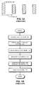
- FIG. 1B is a flowchart illustrating the process of creating model corrections.
- the system starts when a test pattern containing multiple line widths and pitches is received (step 106 ).
- the system creates a mask from the test pattern (step 108 ).
- a test wafer is then formed using the mask (step 110 ).
- the actual line widths and pitches are measured (step 112 ).
- the actual line widths are compared with the desired line widths to determine the error in the actual line widths (step 114 ).
- the measured error is used to calibrate the model so that the model will more accurately approximate actual line widths (step 116 ).
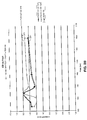
- FIG. 1C is a graph plotting actual line width versus pitch for a target line width of 160 nm.
- Target CD 118 indicates the target line width of 160 nm.
- the region labeled valuable data 120 provides more useful information for the model.
- the regions labeled less valuable data 122 are far removed from target CD 118 and are in non-linear regions so that model corrections are difficult to compute.
- One embodiment of the invention provides a system for using a test pattern to calibrate a model of a manufacturing process for an integrated circuit.
- the system operates by first receiving a basic test pattern and then performing optical proximity correction (OPC) on this basic test pattern using an optical model.
- OPC optical proximity correction
- This optical proximity correction creates a partially corrected or modified test pattern.
- This partially corrected test pattern is optical proximity effect free.
- a mask is generated from the partially corrected test pattern and then a test wafer is created using the mask.
- the system measures features on the test wafer to determine a difference between the desired width and the width on the test wafer.
- the system calibrates the model using this difference.
- the basic test pattern includes multiple line widths and for each line width the basic test pattern includes multiple line pitches.
- performing optical proximity correction on the basic test pattern compensates for optical effects involved in creating the test wafer.
- the difference between the partially corrected test pattern and the test wafer includes multiple measurements for each line width and pitch.
- the system sorts the measurements according to the expected line width.
- the system compares the expected line width at a specified pitch with the actual line width at the specified pitch to determine the model error, thereby creating measurements closer to the target dimension and providing more information for accurate OPC.
- the system calibrates the model to compensate for the model error allowing easier judgment about the model accuracy by a process engineer.
- receiving the test pattern includes designing the test pattern with a plurality of lines having different widths and pitches arranged in a grid.
- FIG. 1A illustrates line width and pitch.
- FIG. 1B is a flowchart illustrating the process of calibrating a model.
- FIG. 1C is a graph plotting actual line width versus pitch for a target line width.
- FIG. 2A is a flowchart illustrating the process of calibrating an optical model in accordance with an embodiment of the invention.
- FIG. 2B is a graph plotting actual line width versus pitch for a target line width in accordance with an embodiment of the invention.
- FIG. 3 illustrates model calibration in accordance with an embodiment of the invention.
- FIG. 2A is a flowchart illustrating the process of calibrating an optical model in accordance with an embodiment of the invention.
- An optical model is a model created by a model generator such as ModelGenTM, which corrects for optical effects while creating an integrated circuit. These effects include numerical aperture (NA), wavelength ( ⁇ ), and sigma ( ⁇ ). Calibrating this model with a model calibrator such as ModelCalTM allows the calibrated model to compensate for resist and/or etch effects.
- ModelGenTM and ModelCalTM are trademarks or registered trademarks of Numerical Technologies, Inc. of San Jose, Calif.
- the system starts when a basic test pattern containing multiple line widths and pitches is received (step 202 ). Next, the system performs optical proximity correction on the test pattern (step 204 ).
- a mask is then created from the test pattern (step 206 ). After creating the mask, a test wafer is formed using the mask (step 208 ).
- the actual line widths and pitches are measured (step 210 ).
- the actual line widths are compared with the desired line widths to determine the error in the actual line widths (step 212 ).
- the model is calibrated for resist and/or etch effects so that the model will create line widths closer to the desired line widths (step 214 ). Since optical proximity correction has been performed on the test pattern, the corrections are more accurate and determined with fewer measurements and calculations.
- FIG. 2B is a graph plotting actual line width versus pitch for a target line width in accordance with an embodiment of the invention.
- Curve 218 illustrates the predicted critical dimension (CD) from the optical model.
- Curve 220 illustrates the predicted CD from the calibrated model.
- Curve 222 illustrates the measured CD on a wafer. As illustrated, the differences from these curves to target CD 216 are relatively small and are more linear.
- FIG. 3 illustrates model calibration 302 in accordance with an embodiment of the invention.
- the system starts with optical model 304 , test pattern 310 , and wafer critical dimension measurements 306 .
- Optical model 304 applies corrections to mask patterns in a format such as GDSII stream format.
- Test pattern 310 is a pattern of multiple line widths at multiple pitches after optical proximity correction as described above.
- Wafer critical dimension measurements 306 are measurements of the lines on a test wafer corresponding to the lines on test pattern 310 . These wafer critical dimension measurements 306 include resist and/or etch effects.
- Model calibrator 308 receives optical model 304 , test pattern 310 , and wafer critical dimension measurements 306 . Model calibrator 308 then determines corrections to be made to optical model 304 by comparing wafer critical dimension measurements 306 with test pattern 310 to determine the magnitude and direction of the errors. Finally, model calibrator 308 calibrates optical model 304 using the calculated measurements to generate a calibrated model 312 .
- the ModelCalTM software from Numerical Technologies, Inc. can be used.
- a computer readable storage medium which may be any device or medium that can store code and/or data for use by a computer system.
- the transmission medium may include a communications network, such as the Internet.
- the computer instruction signals can include instructions for calibrating a model from CD measurements taken from a test wafer.
Abstract
Description
- 1. Field of the Invention
- The invention relates to the process of manufacturing an integrated circuit. More specifically, the invention relates to a method and an apparatus for calibrating a model related to manufacturing the integrated circuit.
- 2. Related Art
- Integrated circuits can be produced through an optical lithography process that involves creating a mask with a pattern specifying where the various features of the integrated circuit are to be placed and then passing radiation through the mask to expose the pattern on a semiconductor wafer. This pattern defines where the surface of the semiconductor wafer is to be etched or where new material is to be added to create the integrated circuit.
- As the features of an integrated circuit continue to get smaller, resist effects, diffraction and process effects, and other manufacturing process variations become more significant. These diffraction effects cause the actual width of a line to change from the designed width. The pitch of the lines also affects the diffraction and can change the actual line width from the desired width. FIG. 1A illustrates line width and pitch.
Line width 102 is the width of a line, whilepitch 104 is the pitch of the lines. Note thatpitch 104 includesline width 102 and the space between lines. Optionally, pitch can be measured from midpoint of a line to the midpoint of the next line. - Process engineers create a wafer using a test pattern in order to calibrate a computer model of the process. Process engineers then use the computer model to apply corrections to the layout design so that the finished wafer has the desired dimensions after the process is complete. FIG. 1B is a flowchart illustrating the process of creating model corrections. The system starts when a test pattern containing multiple line widths and pitches is received (step 106). Next, the system creates a mask from the test pattern (step 108). A test wafer is then formed using the mask (step 110).
- After the test wafer has been fabricated, the actual line widths and pitches are measured (step 112). Next, the actual line widths are compared with the desired line widths to determine the error in the actual line widths (step 114). Finally, the measured error is used to calibrate the model so that the model will more accurately approximate actual line widths (step 116).
- Except in some special cases, this method is not satisfactory because the measured errors are not linear. This non-linearity causes the model corrections to be understated or overstated, thereby requiring additional test wafers to be created. In the worse case, the corrections never converge on the desired line width. FIG. 1C is a graph plotting actual line width versus pitch for a target line width of 160 nm.
Target CD 118 indicates the target line width of 160 nm. The region labeledvaluable data 120 provides more useful information for the model. However, the regions labeled lessvaluable data 122 are far removed fromtarget CD 118 and are in non-linear regions so that model corrections are difficult to compute. - What is needed is a method and an apparatus to facilitate test pattern design for model calibration and proximity correction that do not exhibit the problems described above.
- One embodiment of the invention provides a system for using a test pattern to calibrate a model of a manufacturing process for an integrated circuit. The system operates by first receiving a basic test pattern and then performing optical proximity correction (OPC) on this basic test pattern using an optical model. This optical proximity correction creates a partially corrected or modified test pattern. This partially corrected test pattern is optical proximity effect free. A mask is generated from the partially corrected test pattern and then a test wafer is created using the mask. The system measures features on the test wafer to determine a difference between the desired width and the width on the test wafer. The system calibrates the model using this difference.
- In one embodiment of the invention, the basic test pattern includes multiple line widths and for each line width the basic test pattern includes multiple line pitches.
- In one embodiment of the invention, performing optical proximity correction on the basic test pattern compensates for optical effects involved in creating the test wafer.
- In one embodiment of the invention, the difference between the partially corrected test pattern and the test wafer includes multiple measurements for each line width and pitch.
- In one embodiment of the invention, the system sorts the measurements according to the expected line width.
- In one embodiment of the invention, the system compares the expected line width at a specified pitch with the actual line width at the specified pitch to determine the model error, thereby creating measurements closer to the target dimension and providing more information for accurate OPC.
- In one embodiment of the invention, the system calibrates the model to compensate for the model error allowing easier judgment about the model accuracy by a process engineer.
- In one embodiment of the invention, receiving the test pattern includes designing the test pattern with a plurality of lines having different widths and pitches arranged in a grid.
- FIG. 1A illustrates line width and pitch.
- FIG. 1B is a flowchart illustrating the process of calibrating a model.
- FIG. 1C is a graph plotting actual line width versus pitch for a target line width.
- FIG. 2A is a flowchart illustrating the process of calibrating an optical model in accordance with an embodiment of the invention.
- FIG. 2B is a graph plotting actual line width versus pitch for a target line width in accordance with an embodiment of the invention.
- FIG. 3 illustrates model calibration in accordance with an embodiment of the invention.
- Creating Model Calibrations
- FIG. 2A is a flowchart illustrating the process of calibrating an optical model in accordance with an embodiment of the invention. An optical model is a model created by a model generator such as ModelGen™, which corrects for optical effects while creating an integrated circuit. These effects include numerical aperture (NA), wavelength (λ), and sigma (σ). Calibrating this model with a model calibrator such as ModelCal™ allows the calibrated model to compensate for resist and/or etch effects. ModelGen™ and ModelCal™ are trademarks or registered trademarks of Numerical Technologies, Inc. of San Jose, Calif. The system starts when a basic test pattern containing multiple line widths and pitches is received (step 202). Next, the system performs optical proximity correction on the test pattern (step 204). Note that performing optical proximity correction on the test pattern at this stage provides more accurate results on the wafer line widths and, therefore, provides better data for model calibration. A mask is then created from the test pattern (step 206). After creating the mask, a test wafer is formed using the mask (step 208).
- After the test wafer has been fabricated, the actual line widths and pitches are measured (step 210). Next, the actual line widths are compared with the desired line widths to determine the error in the actual line widths (step 212). Finally, the model is calibrated for resist and/or etch effects so that the model will create line widths closer to the desired line widths (step 214). Since optical proximity correction has been performed on the test pattern, the corrections are more accurate and determined with fewer measurements and calculations.
- FIG. 2B is a graph plotting actual line width versus pitch for a target line width in accordance with an embodiment of the invention.
Curve 218 illustrates the predicted critical dimension (CD) from the optical model.Curve 220 illustrates the predicted CD from the calibrated model.Curve 222 illustrates the measured CD on a wafer. As illustrated, the differences from these curves to targetCD 216 are relatively small and are more linear. - Model Calibration
- FIG. 3 illustrates
model calibration 302 in accordance with an embodiment of the invention. The system starts withoptical model 304,test pattern 310, and wafercritical dimension measurements 306.Optical model 304 applies corrections to mask patterns in a format such as GDSII stream format.Test pattern 310 is a pattern of multiple line widths at multiple pitches after optical proximity correction as described above. Wafercritical dimension measurements 306 are measurements of the lines on a test wafer corresponding to the lines ontest pattern 310. These wafercritical dimension measurements 306 include resist and/or etch effects. -
Model calibrator 308 receivesoptical model 304,test pattern 310, and wafercritical dimension measurements 306.Model calibrator 308 then determines corrections to be made tooptical model 304 by comparing wafercritical dimension measurements 306 withtest pattern 310 to determine the magnitude and direction of the errors. Finally,model calibrator 308 calibratesoptical model 304 using the calculated measurements to generate a calibratedmodel 312. The ModelCal™ software from Numerical Technologies, Inc. can be used. - The preceding description is presented to enable one to make and use the invention, and is provided in the context of a particular application and its requirements. Various modifications to the disclosed embodiments will be readily apparent, and the general principles defined herein may be applied to other embodiments and applications without departing from the spirit and scope of the invention. The invention can be readily adapted to be used with “next generation” optical lithography techniques including, but not limited to, deep ultraviolet (DUV), extreme ultraviolet (EUV), x-ray, and e-beam with suitable adaptations. Thus, the invention is not intended to be limited to the embodiments shown, but is to be accorded the widest scope consistent with the principles and features disclosed herein.
- The data structures and code described in this detailed description can be stored on a computer readable storage medium, which may be any device or medium that can store code and/or data for use by a computer system. This includes, but is not limited to, magnetic and optical storage devices such as disk drives, magnetic tape, CDs (compact discs) and DVDs (digital versatile discs or digital video discs), and computer instruction signals embodied in a transmission medium (with or without a carrier wave upon which the signals are modulated). For example, the transmission medium may include a communications network, such as the Internet. In one embodiment of the invention, the computer instruction signals can include instructions for calibrating a model from CD measurements taken from a test wafer.
- The foregoing descriptions of embodiments of the invention have been presented for purposes of illustration and description only. They are not intended to be exhaustive or to limit the invention to the forms disclosed. The scope of the invention is defined by the appended claims.
Claims (29)
Priority Applications (1)
| Application Number | Priority Date | Filing Date | Title |
|---|---|---|---|
| US10/116,286 US20030192015A1 (en) | 2002-04-04 | 2002-04-04 | Method and apparatus to facilitate test pattern design for model calibration and proximity correction |
Applications Claiming Priority (1)
| Application Number | Priority Date | Filing Date | Title |
|---|---|---|---|
| US10/116,286 US20030192015A1 (en) | 2002-04-04 | 2002-04-04 | Method and apparatus to facilitate test pattern design for model calibration and proximity correction |
Publications (1)
| Publication Number | Publication Date |
|---|---|
| US20030192015A1 true US20030192015A1 (en) | 2003-10-09 |
Family
ID=28673941
Family Applications (1)
| Application Number | Title | Priority Date | Filing Date |
|---|---|---|---|
| US10/116,286 Abandoned US20030192015A1 (en) | 2002-04-04 | 2002-04-04 | Method and apparatus to facilitate test pattern design for model calibration and proximity correction |
Country Status (1)
| Country | Link |
|---|---|
| US (1) | US20030192015A1 (en) |
Cited By (38)
| Publication number | Priority date | Publication date | Assignee | Title |
|---|---|---|---|---|
| US20050257188A1 (en) * | 2004-04-28 | 2005-11-17 | Toshiya Kotani | Pattern correcting method, mask making method, method of manufacturing semiconductor device, pattern correction system, and computer-readable recording medium having pattern correction program recorded therein |
| US20070079278A1 (en) * | 2005-10-05 | 2007-04-05 | Yasushi Tanaka | Method and apparatus for reducing OPC model errors |
| US20080022237A1 (en) * | 2002-08-15 | 2008-01-24 | Eric Adler | Device modeling for proximity effects |
| WO2008137922A1 (en) * | 2007-05-07 | 2008-11-13 | Kla-Tencor Corporation | Computer-implemented methods, systems, and computer-readable media for determining a model for predicting printability of reticle features on a wafer |
| US20080295059A1 (en) * | 2007-05-21 | 2008-11-27 | Hynix Semiconductor Inc. | Method for Correcting Optical Proximity Effect |
| US7646906B2 (en) | 2004-01-29 | 2010-01-12 | Kla-Tencor Technologies Corp. | Computer-implemented methods for detecting defects in reticle design data |
| US7676077B2 (en) | 2005-11-18 | 2010-03-09 | Kla-Tencor Technologies Corp. | Methods and systems for utilizing design data in combination with inspection data |
| US20100070944A1 (en) * | 2008-09-16 | 2010-03-18 | United Microelectronics Corp. | Method for constructing opc model |
| US7689966B2 (en) | 2004-09-14 | 2010-03-30 | Kla-Tencor Technologies Corp. | Methods, systems, and carrier media for evaluating reticle layout data |
| US7711514B2 (en) | 2007-08-10 | 2010-05-04 | Kla-Tencor Technologies Corp. | Computer-implemented methods, carrier media, and systems for generating a metrology sampling plan |
| US7769225B2 (en) | 2005-08-02 | 2010-08-03 | Kla-Tencor Technologies Corp. | Methods and systems for detecting defects in a reticle design pattern |
| US7796804B2 (en) | 2007-07-20 | 2010-09-14 | Kla-Tencor Corp. | Methods for generating a standard reference die for use in a die to standard reference die inspection and methods for inspecting a wafer |
| US7877722B2 (en) | 2006-12-19 | 2011-01-25 | Kla-Tencor Corp. | Systems and methods for creating inspection recipes |
| US7975245B2 (en) | 2007-08-20 | 2011-07-05 | Kla-Tencor Corp. | Computer-implemented methods for determining if actual defects are potentially systematic defects or potentially random defects |
| US7999920B2 (en) | 2007-08-22 | 2011-08-16 | Asml Netherlands B.V. | Method of performing model-based scanner tuning |
| US8041103B2 (en) | 2005-11-18 | 2011-10-18 | Kla-Tencor Technologies Corp. | Methods and systems for determining a position of inspection data in design data space |
| US8112241B2 (en) | 2009-03-13 | 2012-02-07 | Kla-Tencor Corp. | Methods and systems for generating an inspection process for a wafer |
| US8139844B2 (en) | 2008-04-14 | 2012-03-20 | Kla-Tencor Corp. | Methods and systems for determining a defect criticality index for defects on wafers |
| US8194968B2 (en) | 2007-01-05 | 2012-06-05 | Kla-Tencor Corp. | Methods and systems for using electrical information for a device being fabricated on a wafer to perform one or more defect-related functions |
| US8213704B2 (en) | 2007-05-09 | 2012-07-03 | Kla-Tencor Corp. | Methods and systems for detecting defects in a reticle design pattern |
| US20120229786A1 (en) * | 2011-03-11 | 2012-09-13 | Asml Netherlands B.V. | Method of controlling a lithographic apparatus, device manufacturing method, lithographic apparatus, computer program product and method of improving a mathematical model of a lithographic process |
| CN102759862A (en) * | 2011-04-28 | 2012-10-31 | 中芯国际集成电路制造(上海)有限公司 | Optical proximity correction method |
| TWI421908B (en) * | 2008-09-18 | 2014-01-01 | United Microelectronics Corp | Method for constructing opc model |
| US8775101B2 (en) | 2009-02-13 | 2014-07-08 | Kla-Tencor Corp. | Detecting defects on a wafer |
| US8781781B2 (en) | 2010-07-30 | 2014-07-15 | Kla-Tencor Corp. | Dynamic care areas |
| US8826200B2 (en) | 2012-05-25 | 2014-09-02 | Kla-Tencor Corp. | Alteration for wafer inspection |
| US8831334B2 (en) | 2012-01-20 | 2014-09-09 | Kla-Tencor Corp. | Segmentation for wafer inspection |
| US8923600B2 (en) | 2005-11-18 | 2014-12-30 | Kla-Tencor Technologies Corp. | Methods and systems for utilizing design data in combination with inspection data |
| US9053527B2 (en) | 2013-01-02 | 2015-06-09 | Kla-Tencor Corp. | Detecting defects on a wafer |
| US9087367B2 (en) | 2011-09-13 | 2015-07-21 | Kla-Tencor Corp. | Determining design coordinates for wafer defects |
| US9092846B2 (en) | 2013-02-01 | 2015-07-28 | Kla-Tencor Corp. | Detecting defects on a wafer using defect-specific and multi-channel information |
| US9134254B2 (en) | 2013-01-07 | 2015-09-15 | Kla-Tencor Corp. | Determining a position of inspection system output in design data space |
| US9170211B2 (en) | 2011-03-25 | 2015-10-27 | Kla-Tencor Corp. | Design-based inspection using repeating structures |
| US9189844B2 (en) | 2012-10-15 | 2015-11-17 | Kla-Tencor Corp. | Detecting defects on a wafer using defect-specific information |
| US9310320B2 (en) | 2013-04-15 | 2016-04-12 | Kla-Tencor Corp. | Based sampling and binning for yield critical defects |
| US9311698B2 (en) | 2013-01-09 | 2016-04-12 | Kla-Tencor Corp. | Detecting defects on a wafer using template image matching |
| US9659670B2 (en) | 2008-07-28 | 2017-05-23 | Kla-Tencor Corp. | Computer-implemented methods, computer-readable media, and systems for classifying defects detected in a memory device area on a wafer |
| US9865512B2 (en) | 2013-04-08 | 2018-01-09 | Kla-Tencor Corp. | Dynamic design attributes for wafer inspection |
Citations (8)
| Publication number | Priority date | Publication date | Assignee | Title |
|---|---|---|---|---|
| US20020015899A1 (en) * | 2000-05-01 | 2002-02-07 | Chen Jang Fung | Hybrid phase-shift mask |
| US20030008215A1 (en) * | 2001-07-03 | 2003-01-09 | Maharaj Mukherjee | Method for correcting optical proximity effects in a lithographic process using the radius of curvature of shapes on a mask |
| US20030046653A1 (en) * | 2001-08-31 | 2003-03-06 | Numerical Technologies, Inc. | Microloading effect correction |
| US20030082463A1 (en) * | 2001-10-09 | 2003-05-01 | Thomas Laidig | Method of two dimensional feature model calibration and optimization |
| US20030088847A1 (en) * | 2001-11-07 | 2003-05-08 | Numerical Technologies, Inc. | Method of incorporating lens aberration information into various process flows |
| US20030115569A1 (en) * | 2001-11-26 | 2003-06-19 | Atsuhiko Ikeuchi | Method and system for optical proximity correction |
| US6602728B1 (en) * | 2001-01-05 | 2003-08-05 | International Business Machines Corporation | Method for generating a proximity model based on proximity rules |
| US20030149955A1 (en) * | 2001-05-10 | 2003-08-07 | Hidetoshi Ohnuma | Rule-based opc evaluating method and simulation base opc model evaluating method |
-
2002
- 2002-04-04 US US10/116,286 patent/US20030192015A1/en not_active Abandoned
Patent Citations (8)
| Publication number | Priority date | Publication date | Assignee | Title |
|---|---|---|---|---|
| US20020015899A1 (en) * | 2000-05-01 | 2002-02-07 | Chen Jang Fung | Hybrid phase-shift mask |
| US6602728B1 (en) * | 2001-01-05 | 2003-08-05 | International Business Machines Corporation | Method for generating a proximity model based on proximity rules |
| US20030149955A1 (en) * | 2001-05-10 | 2003-08-07 | Hidetoshi Ohnuma | Rule-based opc evaluating method and simulation base opc model evaluating method |
| US20030008215A1 (en) * | 2001-07-03 | 2003-01-09 | Maharaj Mukherjee | Method for correcting optical proximity effects in a lithographic process using the radius of curvature of shapes on a mask |
| US20030046653A1 (en) * | 2001-08-31 | 2003-03-06 | Numerical Technologies, Inc. | Microloading effect correction |
| US20030082463A1 (en) * | 2001-10-09 | 2003-05-01 | Thomas Laidig | Method of two dimensional feature model calibration and optimization |
| US20030088847A1 (en) * | 2001-11-07 | 2003-05-08 | Numerical Technologies, Inc. | Method of incorporating lens aberration information into various process flows |
| US20030115569A1 (en) * | 2001-11-26 | 2003-06-19 | Atsuhiko Ikeuchi | Method and system for optical proximity correction |
Cited By (49)
| Publication number | Priority date | Publication date | Assignee | Title |
|---|---|---|---|---|
| US20080022237A1 (en) * | 2002-08-15 | 2008-01-24 | Eric Adler | Device modeling for proximity effects |
| US7646906B2 (en) | 2004-01-29 | 2010-01-12 | Kla-Tencor Technologies Corp. | Computer-implemented methods for detecting defects in reticle design data |
| US20050257188A1 (en) * | 2004-04-28 | 2005-11-17 | Toshiya Kotani | Pattern correcting method, mask making method, method of manufacturing semiconductor device, pattern correction system, and computer-readable recording medium having pattern correction program recorded therein |
| US7337426B2 (en) * | 2004-04-28 | 2008-02-26 | Kabushiki Kaisha Toshiba | Pattern correcting method, mask making method, method of manufacturing semiconductor device, pattern correction system, and computer-readable recording medium having pattern correction program recorded therein |
| US7689966B2 (en) | 2004-09-14 | 2010-03-30 | Kla-Tencor Technologies Corp. | Methods, systems, and carrier media for evaluating reticle layout data |
| US7769225B2 (en) | 2005-08-02 | 2010-08-03 | Kla-Tencor Technologies Corp. | Methods and systems for detecting defects in a reticle design pattern |
| US7325225B2 (en) | 2005-10-05 | 2008-01-29 | Yasushi Tanaka | Method and apparatus for reducing OPC model errors |
| US20070079278A1 (en) * | 2005-10-05 | 2007-04-05 | Yasushi Tanaka | Method and apparatus for reducing OPC model errors |
| US7676077B2 (en) | 2005-11-18 | 2010-03-09 | Kla-Tencor Technologies Corp. | Methods and systems for utilizing design data in combination with inspection data |
| US8923600B2 (en) | 2005-11-18 | 2014-12-30 | Kla-Tencor Technologies Corp. | Methods and systems for utilizing design data in combination with inspection data |
| US8041103B2 (en) | 2005-11-18 | 2011-10-18 | Kla-Tencor Technologies Corp. | Methods and systems for determining a position of inspection data in design data space |
| US8139843B2 (en) | 2005-11-18 | 2012-03-20 | Kla-Tencor Technologies Corp. | Methods and systems for utilizing design data in combination with inspection data |
| US7877722B2 (en) | 2006-12-19 | 2011-01-25 | Kla-Tencor Corp. | Systems and methods for creating inspection recipes |
| US8194968B2 (en) | 2007-01-05 | 2012-06-05 | Kla-Tencor Corp. | Methods and systems for using electrical information for a device being fabricated on a wafer to perform one or more defect-related functions |
| WO2008137922A1 (en) * | 2007-05-07 | 2008-11-13 | Kla-Tencor Corporation | Computer-implemented methods, systems, and computer-readable media for determining a model for predicting printability of reticle features on a wafer |
| US8213704B2 (en) | 2007-05-09 | 2012-07-03 | Kla-Tencor Corp. | Methods and systems for detecting defects in a reticle design pattern |
| US20080295059A1 (en) * | 2007-05-21 | 2008-11-27 | Hynix Semiconductor Inc. | Method for Correcting Optical Proximity Effect |
| US7827520B2 (en) * | 2007-05-21 | 2010-11-02 | Hynix Semiconductor Inc. | Method for correcting optical proximity effect |
| US8204296B2 (en) | 2007-07-20 | 2012-06-19 | Kla-Tencor Corp. | Methods for generating a standard reference die for use in a die to standard reference die inspection and methods for inspecting a wafer |
| US7796804B2 (en) | 2007-07-20 | 2010-09-14 | Kla-Tencor Corp. | Methods for generating a standard reference die for use in a die to standard reference die inspection and methods for inspecting a wafer |
| US7711514B2 (en) | 2007-08-10 | 2010-05-04 | Kla-Tencor Technologies Corp. | Computer-implemented methods, carrier media, and systems for generating a metrology sampling plan |
| US7975245B2 (en) | 2007-08-20 | 2011-07-05 | Kla-Tencor Corp. | Computer-implemented methods for determining if actual defects are potentially systematic defects or potentially random defects |
| US11372337B2 (en) | 2007-08-22 | 2022-06-28 | Asml Netherlands B.V. | Method of performing model-based scanner tuning |
| US7999920B2 (en) | 2007-08-22 | 2011-08-16 | Asml Netherlands B.V. | Method of performing model-based scanner tuning |
| US9158208B2 (en) | 2007-08-22 | 2015-10-13 | Asml Netherlands B.V. | Method of performing model-based scanner tuning |
| US10795266B2 (en) | 2007-08-22 | 2020-10-06 | Asml Netherlands B.V. | Method of performing model-based scanner tuning |
| US9921485B2 (en) | 2007-08-22 | 2018-03-20 | Asml Netherlands B.V. | Method of performing model-based scanner tuning |
| US8139844B2 (en) | 2008-04-14 | 2012-03-20 | Kla-Tencor Corp. | Methods and systems for determining a defect criticality index for defects on wafers |
| US9659670B2 (en) | 2008-07-28 | 2017-05-23 | Kla-Tencor Corp. | Computer-implemented methods, computer-readable media, and systems for classifying defects detected in a memory device area on a wafer |
| US8166424B2 (en) * | 2008-09-16 | 2012-04-24 | United Microelectronics Corp. | Method for constructing OPC model |
| US20100070944A1 (en) * | 2008-09-16 | 2010-03-18 | United Microelectronics Corp. | Method for constructing opc model |
| TWI421908B (en) * | 2008-09-18 | 2014-01-01 | United Microelectronics Corp | Method for constructing opc model |
| US8775101B2 (en) | 2009-02-13 | 2014-07-08 | Kla-Tencor Corp. | Detecting defects on a wafer |
| US8112241B2 (en) | 2009-03-13 | 2012-02-07 | Kla-Tencor Corp. | Methods and systems for generating an inspection process for a wafer |
| US8781781B2 (en) | 2010-07-30 | 2014-07-15 | Kla-Tencor Corp. | Dynamic care areas |
| US20120229786A1 (en) * | 2011-03-11 | 2012-09-13 | Asml Netherlands B.V. | Method of controlling a lithographic apparatus, device manufacturing method, lithographic apparatus, computer program product and method of improving a mathematical model of a lithographic process |
| US9696635B2 (en) * | 2011-03-11 | 2017-07-04 | Asml Netherlands B.V. | Method of controlling a lithographic apparatus, device manufacturing method, lithographic apparatus, computer program product and method of improving a mathematical model of a lithographic process |
| US9170211B2 (en) | 2011-03-25 | 2015-10-27 | Kla-Tencor Corp. | Design-based inspection using repeating structures |
| CN102759862A (en) * | 2011-04-28 | 2012-10-31 | 中芯国际集成电路制造(上海)有限公司 | Optical proximity correction method |
| US9087367B2 (en) | 2011-09-13 | 2015-07-21 | Kla-Tencor Corp. | Determining design coordinates for wafer defects |
| US8831334B2 (en) | 2012-01-20 | 2014-09-09 | Kla-Tencor Corp. | Segmentation for wafer inspection |
| US8826200B2 (en) | 2012-05-25 | 2014-09-02 | Kla-Tencor Corp. | Alteration for wafer inspection |
| US9189844B2 (en) | 2012-10-15 | 2015-11-17 | Kla-Tencor Corp. | Detecting defects on a wafer using defect-specific information |
| US9053527B2 (en) | 2013-01-02 | 2015-06-09 | Kla-Tencor Corp. | Detecting defects on a wafer |
| US9134254B2 (en) | 2013-01-07 | 2015-09-15 | Kla-Tencor Corp. | Determining a position of inspection system output in design data space |
| US9311698B2 (en) | 2013-01-09 | 2016-04-12 | Kla-Tencor Corp. | Detecting defects on a wafer using template image matching |
| US9092846B2 (en) | 2013-02-01 | 2015-07-28 | Kla-Tencor Corp. | Detecting defects on a wafer using defect-specific and multi-channel information |
| US9865512B2 (en) | 2013-04-08 | 2018-01-09 | Kla-Tencor Corp. | Dynamic design attributes for wafer inspection |
| US9310320B2 (en) | 2013-04-15 | 2016-04-12 | Kla-Tencor Corp. | Based sampling and binning for yield critical defects |
Similar Documents
| Publication | Publication Date | Title |
|---|---|---|
| US20030192015A1 (en) | Method and apparatus to facilitate test pattern design for model calibration and proximity correction | |
| US6684382B2 (en) | Microloading effect correction | |
| US7673281B2 (en) | Pattern evaluation method and evaluation apparatus and pattern evaluation program | |
| US20200233317A1 (en) | Metrology Method for a Semiconductor Manufacturing Process | |
| KR101059265B1 (en) | How to correct mask | |
| US7480890B2 (en) | Method for correcting and configuring optical mask pattern | |
| US11200362B2 (en) | 3D resist profile aware resolution enhancement techniques | |
| US7426712B2 (en) | Lithography simulation method and recording medium | |
| US7325225B2 (en) | Method and apparatus for reducing OPC model errors | |
| US8607168B2 (en) | Contour alignment for model calibration | |
| US9484186B2 (en) | Modeling and correcting short-range and long-range effects in E-beam lithography | |
| US20230099105A1 (en) | Reduction or elimination of pattern placement error in metrology measurements | |
| US20100011325A1 (en) | Method and apparatus for determining the effect of process variations | |
| US20090132992A1 (en) | Statistical optical proximity correction | |
| JP2005055563A (en) | Mask correction program, mask correction method and method for manufacturing mask | |
| US20050050512A1 (en) | Method for projection of a circuit pattern, which is arranged on a mask, onto a semiconductor wafer | |
| US20100082313A1 (en) | Optical Lithographic Process Model Calibration | |
| CN114925635A (en) | OPC model data weight setting method | |
| JP4551937B2 (en) | Pattern formation method | |
| CN112099316B (en) | Correction method and system of optical proximity correction model | |
| JP4691840B2 (en) | Mask pattern generation method and photomask | |
| Laske et al. | In-depth overlay contribution analysis of a poly-layer reticle | |
| TWI631415B (en) | Method of simultaneous lithography and etch correction flow | |
| US20220252991A1 (en) | Method for overlay control based on a semiconductor device pattern, and method and system for generating a photomask | |
| US20090191473A1 (en) | Photomask manufacturing method, photomask manufacturing system, and device manufacturing method |
Legal Events
| Date | Code | Title | Description |
|---|---|---|---|
| AS | Assignment |
Owner name: NUMERICAL TECHNOLOGIES, INC., CALIFORNIA Free format text: ASSIGNMENT OF ASSIGNORS INTEREST;ASSIGNOR:LIU, HUA-YU;REEL/FRAME:012763/0213 Effective date: 20020402 |
|
| STCB | Information on status: application discontinuation |
Free format text: ABANDONED -- FAILURE TO RESPOND TO AN OFFICE ACTION |
|
| AS | Assignment |
Owner name: SYNOPSYS, INC., CALIFORNIA Free format text: ASSIGNMENT OF ASSIGNORS INTEREST;ASSIGNOR:SYNOPSYS MERGER HOLDINGS LLC;REEL/FRAME:015653/0738 Effective date: 20041223 |
|
| AS | Assignment |
Owner name: SYNOPSYS MERGER HOLDINGS, LLC., CALIFORNIA Free format text: ASSIGNMENT OF ASSIGNORS INTEREST;ASSIGNOR:NUMERICAL TECHNOLOGIES, INC.;REEL/FRAME:023736/0273 Effective date: 20091216 |
|
| AS | Assignment |
Owner name: SYNOPSYS MERGER HOLDINGS, LLC., CALIFORNIA Free format text: CORRECTIVE ASSIGNMENT TO CORRECT THE ASSIGNOR DOCUMENT DATE SHOULD BE 12/20/2004 PREVIOUSLY RECORDED ON REEL 023736 FRAME 0275. ASSIGNOR(S) HEREBY CONFIRMS THE ASSIGNMENT OF ASSIGNORS INTEREST;ASSIGNOR:NUMERICAL TECHNOLOGIES, INC.;REEL/FRAME:038060/0911 Effective date: 20041220 |