US20030191993A1 - Semiconductor device for memory test with changing address information - Google Patents
Semiconductor device for memory test with changing address information Download PDFInfo
- Publication number
- US20030191993A1 US20030191993A1 US10/235,638 US23563802A US2003191993A1 US 20030191993 A1 US20030191993 A1 US 20030191993A1 US 23563802 A US23563802 A US 23563802A US 2003191993 A1 US2003191993 A1 US 2003191993A1
- Authority
- US
- United States
- Prior art keywords
- address
- test
- address information
- data
- memory
- Prior art date
- Legal status (The legal status is an assumption and is not a legal conclusion. Google has not performed a legal analysis and makes no representation as to the accuracy of the status listed.)
- Abandoned
Links
- 238000012360 testing method Methods 0.000 title claims abstract description 108
- 239000004065 semiconductor Substances 0.000 title claims abstract description 70
- 238000006243 chemical reaction Methods 0.000 claims abstract description 6
- 238000010586 diagram Methods 0.000 description 22
- 230000005540 biological transmission Effects 0.000 description 10
- 239000000470 constituent Substances 0.000 description 5
- 238000011056 performance test Methods 0.000 description 4
- 230000000694 effects Effects 0.000 description 3
- 230000006870 function Effects 0.000 description 2
- 102100036848 C-C motif chemokine 20 Human genes 0.000 description 1
- 102100035353 Cyclin-dependent kinase 2-associated protein 1 Human genes 0.000 description 1
- 230000007257 malfunction Effects 0.000 description 1
- 238000004904 shortening Methods 0.000 description 1
- 239000000758 substrate Substances 0.000 description 1
Images


Classifications
-
- G—PHYSICS
- G11—INFORMATION STORAGE
- G11C—STATIC STORES
- G11C29/00—Checking stores for correct operation ; Subsequent repair; Testing stores during standby or offline operation
- G11C29/04—Detection or location of defective memory elements, e.g. cell constructio details, timing of test signals
- G11C29/08—Functional testing, e.g. testing during refresh, power-on self testing [POST] or distributed testing
- G11C29/12—Built-in arrangements for testing, e.g. built-in self testing [BIST] or interconnection details
- G11C29/18—Address generation devices; Devices for accessing memories, e.g. details of addressing circuits
-
- G—PHYSICS
- G11—INFORMATION STORAGE
- G11C—STATIC STORES
- G11C29/00—Checking stores for correct operation ; Subsequent repair; Testing stores during standby or offline operation
-
- G—PHYSICS
- G11—INFORMATION STORAGE
- G11C—STATIC STORES
- G11C2207/00—Indexing scheme relating to arrangements for writing information into, or reading information out from, a digital store
- G11C2207/10—Aspects relating to interfaces of memory device to external buses
- G11C2207/104—Embedded memory devices, e.g. memories with a processing device on the same die or ASIC memory designs
Definitions
- the present invention relates to a semiconductor device for memory test with changing address information provided with an address decoder and an internal memory having a function for producing the data of a memory array region by the address decoder and, in particular, to a semiconductor device for memory test with changing address information in which the memory array region of one internal memory is divided into independent regions that do not affect each other and in which the self-test of the internal memory itself is conducted.
- a semiconductor memory device is formed on the same substrate along with a CPU and the like or is formed as one chip along with a CPU and the like.
- the performance test of the semiconductor memory device is conducted, the performance test is conducted by the use of a tester.
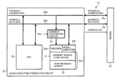
- FIG. 13 is a block diagram to show one example of a semiconductor integrated circuit in the related art with a tester.
- a reference character 11 denotes a semiconductor integrated circuit that has an internal memory 11 b as a semiconductor memory device;
- a reference character 11 a denotes a CPU mounted in the semiconductor integrated circuit 11 ;
- a reference character 11 b denotes the internal memory that has a decoder 111 , a sense amplifier 112 , and a memory array 113 ;
- reference characters 11 c and 11 d denote an internal address bus and an internal data bus that are mounted in the semiconductor integrated circuit 11 ;
- a reference character 12 denotes a tester used for testing the internal memory 11 b ;
- a reference character 13 denotes an external bus that has an external address bus 13 a and an external data bus 13 b , wherein the external address bus 13 a and the external data bus 13 b are the external address bus and the external data bus that connect the semiconductor integrated circuit 11 to the tester 12 , respectively
- FIG. 14 is a flow chart describing the test of the internal memory in the semiconductor integrated circuit in FIG. 13 and a test operation will be described with reference to this drawing.
- a test program is stored in the tester 12 (step ST 1 ). Then, the CPU 11 a fetches an instruction code of the test program on the tester 12 via the external bus 13 (step ST 2 ). If the instruction code fetched is a data read request for the internal memory 11 b (step ST 3 ), the CPU 11 a reads data from the internal memory 11 b in accordance with the address received via the external address bus 13 a and the internal address bus 11 c and outputs the data to the internal data bus 11 d (step ST 4 ). The data on the internal data bus 11 d is given to the tester 12 as output data via the external data bus 13 b .
- the instruction code fetched is not a data test instruction in the step ST 3 , the program is returned to the step ST 2 .
- the tester 12 compares an expected value that is set in advance with the output data described above (step ST 5 ). If the expected value does not agree with the output data, it is judged an error and the test is finished. If the expected value agrees with the output data, it is judged whether or not all of the test programs are finished (step ST 6 ). If all of the test programs are finished, the test is finished. On the other hand, if all of the test programs are not finished, the program is returned to the step ST 2 and the test is continued (the CPU 11 a again fetches the instruction code of the test program).
- the semiconductor memory device has been increased in speed and capacity as a transistor has been patterned more finely. Further, as a progress has been made in increasing the speed and capacity of the semiconductor memory device, it has become difficult to test the performance of the semiconductor memory device by the use of an ordinary tester (low-cost and low-speed tester). Further, even if a high-speed tester is used, when the data is compared with the expected value by the use of the external bus, as described above, it is difficult to conduct the performance test of the semiconductor memory device (internal memory 11 b ) because of the performance capability of the external bus. In addition, with the increasing capacity of the semiconductor memory device, the test vector of the test program is increased in size and the time required to make the test vector like this can not be neglected.
- the so-called self-test is conducted in which a program is previously stored in the internal memory itself of the semiconductor memory device and in which a CPU is operated in accordance with the program to thereby conduct the performance test of the semiconductor memory device.
- FIG. 15 is a block diagram to show another example of the semiconductor integrated circuit in the related art.
- a reference character 11 e denotes an internal memory
- a reference character 121 denotes a decoder
- a reference character 122 denotes a sense amplifier that is provided separately from the internal memory 11 b .
- the same constituent parts as those in FIG. 3 are denoted by the same reference characters and their descriptions will be omitted.
- FIG. 16 is a flow chart describing the self-test of the internal memory of the semiconductor integrated circuit in FIG. 15, and the self-test will be described with reference to this drawing.
- the semiconductor integrated circuit 11 is provided with the internal memory 11 e in addition to the internal memory 11 b .
- the internal memory 11 e has a decoder 121 , a sense amplifier 122 , and a memory array 123 .
- the internal memory 11 b is an object to be tested and a test program is stored in the memory array 123 of the internal memory 11 e.
- test program is stored in the tester 12 (step ST 11 ). Then, the test program on the tester 12 is transferred to the internal memory 11 e via an internal address bus 11 c and an internal data bus 11 d at the operable seed of the external bus 13 (step ST 12 ).
- a CPU 11 a fetches the instruction code of the test program stored in the internal memory 11 e via the internal bus (step ST 13 ).
- step ST 14 If the instruction code fetched is the data test instruction of the internal memory 11 b (step ST 14 ), the CPU 11 a reads data from the internal memory 11 b in accordance with the data test instruction and outputs the data to the internal data bus 11 d (step ST 15 ).
- the instruction code fetched in the step ST 14 is not the data test instruction, the program is returned to the step ST 13 .
- the CPU 11 a compares the data on the internal data bus lid with an expected value that is set in advance (step ST 16 ). If the data does not agree with the expected value, the CPU 11 a outputs an error flag to a signal line by the use of a port (input/output terminal) (step ST 17 ). At this time, the error flag is outputted at the operable speed of the signal line. The tester 12 recognizes an error by the error flag (step ST 18 ) and finishes the test (error finish).
- step ST 19 the CPU 11 a judges whether or not the all of the test programs are finished. At this time, if the CPU 11 a judges that all of the test programs are finished, the test is normally finished. If the all of the test programs are not finished, the program is returned to the step ST 13 and the test is continued (the CPU 11 a again fetches the instruction code of the test program).
- the present invention has been made to solve the above-mentioned problems. It is the object of the present invention to provide a semiconductor device for memory test with changing address information which is provided with an address decoder and an internal memory having a function of getting the data of a memory array region by the address decoder and in which the memory array region is divided into regions, which are independent of and do not affect each other, by the one internal memory and a small number of hardware to conduct the self-test of the internal memory itself.
- a semiconductor device for memory test with changing address information in accordance with the present invention includes a memory array into which data based on predetermined address information are written and read; and address converting means that makes a predetermined conversion of a part or the whole of the address information to convert the address information into new address information for specifying a desired region in the memory array.
- a semiconductor device for memory test with changing address information in accordance with the present invention includes a memory array into which data based on predetermined address information are written and read; and a plurality of blocks for a test each of which has: address converting means that operates according to an inputted control signal to make a predetermined conversion of a part or the whole of the address information to thereby convert the address information into new address information for specifying a desired region in the memory array; at least one register that stores the expected value of data in the memory array; and comparing means that compares data read from one region in the memory array specified by the new address information generated by the address converting means with the expected value read from the register and outputs the result of comparison.
- FIG. 1 is a block diagram to show the configuration of a semiconductor device for memory test with changing address information in accordance with the preferred embodiment 1 of the present invention along with a tester.
- FIG. 2 is a diagram to describe one example of an address converting circuit shown in FIG. 1.
- FIG. 3 is a block diagram to show one example of an address interchanging circuit shown in FIG. 1.
- FIG. 4 is a flow chart to describe the self-test of an internal memory in the semiconductor device shown in FIG. 1.
- FIG. 5 is a diagram to describe another example of an address converting circuit shown in FIG. 1.
- FIG. 6 is a block diagram to show one example of an address inverting circuit shown in FIG. 1.
- FIG. 7 is a diagram to describe still another example of an address converting circuit shown in FIG. 1.
- FIG. 8 is a diagram to show an example of configuration of the address fixing circuit shown in FIG. 7.
- FIG. 9 is a block diagram to show the configuration of a semiconductor device in accordance with the preferred embodiment 2 of the present invention along with a tester.
- FIG. 10 is a flow chart to describe the self-test of an internal memory in a semiconductor device shown in FIG. 9.
- FIG. 11 is a block diagram to show the configuration of a semiconductor device in accordance with the preferred embodiment 3 of the present invention along with a tester.
- FIG. 12 is a flow chart to describe the self-test of an internal memory in a semiconductor device shown in FIG. 11.
- FIG. 13 is a block diagram to show one example of a semiconductor device in the related art along with a tester.
- FIG. 14 is a flow chart to describe the self-test of an internal memory in a semiconductor device shown in FIG. 13.
- FIG. 15 is a block diagram to show another example of a semiconductor device in the related art along with a tester.
- FIG. 16 is a flow chart to describe the self-test of an internal memory in a semiconductor device shown in FIG. 15.
- FIG. 1 is a block diagram to show the configuration of a semiconductor device in accordance with the present invention of the present invention along with a tester.
- a reference character 21 denotes a semiconductor device
- a reference character 22 denotes a CPU
- a reference character 23 denotes an address converting circuit (address converting means)
- a reference character 24 denotes an internal memory that is a semiconductor memory device.
- the CPU 22 is connected to an internal address bus 22 a and an internal data bus 22 b .
- the internal memory 24 is connected to the internal data bus 22 b and, via the address converting circuit 23 , the internal address bus 22 a .
- the internal memory 24 has a memory array 24 a , an address decoder (decoder) 24 b , and a sense amplifier 24 c .
- the memory array 24 a is divided into a memory region to be tested (data region: the second region) 31 and a test program region 32 .
- the address converting circuit 23 selects the memory region to be tested 31 or the test program region 32 in accordance with a control signal for a test C[n] (where n is an integer not smaller than 1).
- FIG. 2 is a diagram to show one example of an address converting circuit in FIG. 1.
- a reference character 33 denotes an address interchanging circuit (address converting means) that outputs an address in which two arbitrary bits of the internal address bus 22 a of M bits interchange with each other to the address decoder 24 b .
- a reference character A[M:0] designates the address of M (where m is an integer not smaller than 1) bits of the internal address bus 22 a .
- a reference character A in [M:0] designates the address of an address bus (hereinafter referred to as an internal memory address) given to the internal memory 24 that is the semiconductor memory device.
- the sense amplifier 24 c is not shown in FIG. 2.
- the address A [M:0] has address bits A[M] to A[ 0 ]. Two arbitrary address bits A[i] and A[j] of these address bits A[M] to A[ 0 ] are given to the address interchanging circuit 33 . Further, the address Ain[M: 0 ] of the internal memory address bus has address bits (hereinafter referred to as an internal address bit) Ain[M] to Ain[ 0 ]. The values of the other address bits except for the above-mentioned address bits A[i] and A[j] are given to the address decoder 24 b as the values of the internal address bits.
- FIG. 3 is a block diagram to show the example of configuration of the address interchanging circuit in FIG. 2.
- the address interchanging circuit 33 has an inverter 33 a and transmission gates 33 b to 33 e .
- the transmission gates 33 b and 33 d are turned on, whereas the transmission gates 33 c and 33 e are turned off.
- the value of the address bit A[i] is given as the internal address bit Ain[i] to the address decoder 24 b .
- the address bit A[j] is given as the internal address bit Ain[j] to the address decoder 24 b .
- the address bit A[i] is equal in logic to the internal address bit Ain[i]
- the address bit A[j] is equal in logic to the internal address bit Ain[j].
- the internal address Ain[M: 0 ] of M bits that is equal in logic to the address A[M: 0 ] of M bits is given to the address decoder 24 b.
- the transmission gates 33 c and 33 e are turned on, whereas the transmission gates 33 b and 33 d are turned off.
- the address bit A[i] is given to the address decoder 24 b as the internal address bit Ain[j].
- the address bit A[j] is given to the address decoder 24 b as the internal address bit Ain[i]. In other words, the address bit A[i] becomes equal in logic to the internal address bit Ain[j] and the address bit A[j] becomes equal in logic to the internal address bit Ain[i].
- FIG. 4 is a flow chart of the self-test of the internal memory in the semiconductor device shown in FIG. 1. The self-test in the present invention will be described with reference to FIG. 4.
- the external buses 13 (the external address bus 13 a and the external data bus 13 b ) are connected to the tester 12 and the port (input/output terminal) of the semiconductor device 21 is connected to the tester 12 by a signal line. Then, a test program is stored in the tester 12 (step ST 21 ).
- the address interchanging circuit 33 outputs, with respect to one address of the internal address bus 22 a , the address which is equal to an inputted value and the address in which the values of the predetermined 2 bits are interchanged with each other to the address decoder 24 b in accordance with the control signal for a test C 1 .
- the memory array 24 a is divided into a memory region to be tested 31 and a test program region 32 (step ST 22 ).
- test program stored in the tester 12 is transferred to the internal memory 24 at the operable speed of the external bus 13 via the internal bus (internal address bus 22 a and internal data bus 22 b ) and is stored in the test program region 32 (step ST 23 ).
- the address interchanging circuit 33 gets the respective data constituting a test vector inputted thereto and interchanges two predetermined bits in the respective addresses corresponding to the respective data to convert them to addresses corresponding to the memory region to be tested 31 .
- the test vector is selectively stored in the memory region to be tested 31 .
- the address specified first by the test vector and the address interchanged are already known. In this manner, by specifying the address for storing the test program such that it does not overlap the address in the memory region to be tested 31 , the test program is stored in the test program region 32 that is independent of and not affected by the memory region to be tested 31 .
- the CPU 22 fetches the instruction code of the test program from the test program region 32 via the internal bus and executes the instruction (step ST 24 ).
- the instruction code fetched by the CPU 22 is a data read request from the memory region to be tested 31 (step ST 25 )
- the CPU 22 reads data from the memory region to be tested 31 and outputs the data to the internal data but 22 b (step ST 26 ).
- the program is returned to the step ST 24 .
- the CPU 22 compares the data on the internal data bus 22 b with an expected value that is set in advance (step ST 27 ). If the data does not agree with the expected value, the CPU 22 outputs an error flag to the signal line by the use of the port (input/output terminal) (step ST 28 ). Here, the error flag is outputted at the operable speed of the signal line. The tester 12 recognizes the error by the error flag (step ST 29 ) and finishes the program as a test error.
- step ST 30 the CPU 22 judges whether or not all of the test programs are finished. At this time, if all of the test programs are finished, the CPU 22 judges that the test normally finished. If all of the test programs are not finished, the program is returned to the step ST 24 , the CPU 22 fetches the instruction code of the test program.
- FIG. 5 is a diagram to describe another example of the address converting circuit shown in FIG. 1.
- an address inverting circuit (address converting means) 34 is used as the address converting circuit 23 .
- the same constituent parts as those shown in FIG. 2 are denoted by the same reference characters.
- one arbitrary address bit A[k] of the address bits A[M] to A[ 0 ] is given to the address inverting circuit 34 .
- the other address bits except for the above-mentioned A[k] are given to the address decoder 24 b as the internal address bits.
- the address bit A[k] is inverted by an address inverting circuit 34 and is given to the address decoder 24 b as the internal address bit Ain[k].
- FIG. 6 is a block diagram to show one example of the address inverting circuit shown in FIG. 5.
- the address inverting circuit 34 has inverters 34 a , 34 b and transmission gates 34 c , 34 d . If a control signal for a test C 2 (here, n 2 ) is an L level, the transmission gate 34 c is turned on and the transmission gate 34 d is turned off. As a result, the address bit A[k] is given to the internal address decoder 24 b as the internal address bit Ain[k]. In other words, the address bit A[k] is equal in logic to the internal address bit Ain[k]. In this manner, the internal address Ain[M: 0 ] that is equal in logic to the address A[M: 0 ] of M bits is given to the address decoder 24 b.
- FIG. 7 is a diagram to describe still another example of the address converting circuit shown in FIG. 1.
- an address fixing circuit (address converting means) 35 is used as the address converting circuit 23 .
- the same constituent parts as those shown in FIG. 2 are denoted by the same reference characters.
- one arbitrary address bit A[l] of the address bits A[M] to A[ 0 ] is given to the address fixing circuit 35 .
- the other address bits except for the above-mentioned A[l] are given to the address decoder 24 b as the internal address bits.
- the address bit A[l] is controlled by an address fixing circuit 35 and is given to the address decoder 24 b as the internal address bit Ain[l].
- FIG. 8 is a diagram to show the example of configuration of the address fixing circuit shown in FIG. 7.
- the OR circuit 35 a outputs the H level irrespective of the address bit A[l].
- the internal address bit Ain[l] is fixed at the H level (for example, logic “1”).
- the internal address Ain [M: 0 ] in which the internal address bit Ain [l] is logic “1” is given to the address decoder 24 b.
- the address converting circuit 23 that divides the memory array region into the memory region to be tested 31 for storing the test data and the test program region 32 for storing the test program, so that it is possible to prevent an increase in a circuit size (quantity of hardware) and to conduct a self-test normally.
- the address converting circuit 23 is not limited to the converting operation described above.
- FIG. 9 is a block diagram to show the configuration of a semiconductor device in accordance with the preferred embodiment 2 of the present invention along with a tester.
- a reference character 41 denotes a semiconductor device and in addition to a CPU 22 , an address converting circuit 23 , and an internal memory 24 , there are provided a register 42 and a data comparator (comparing means) 43 .
- An expected value relating to data read from a memory region to be tested 31 is set in the register 42 (this expected value is set for each memory array 24 a ).
- the data comparator 43 is connected to an internal address bus 22 b and the register 42 .
- FIG. 10 is a flow chart to describe the self-test of the internal memory of the semiconductor device shown in FIG. 9, and the self-test of the present preferred embodiment will be described with reference to FIG. 10.
- the external bus 13 is connected to the tester 12 and the port (input/output terminal) of the semiconductor device 41 is connected to the tester 12 by a signal line.
- a test program is stored in the tester 12 (step ST 31 ).
- a control signal for a test C[n] (where n is any one integer of from 1 to 3) is given to the address converting circuit 23 from the other port of the semiconductor device 41 .
- the memory array 24 a is divided into the test program region 32 and the memory region to be tested 31 in accordance with the control signal for a test C[n].
- an expected value relating to data read from the memory region to be tested 31 is set at a register 42 from the port of the semiconductor device 41 (step ST 33 : a signal line (route) when the expected value is set at the register 42 from the port is not shown in FIG. 9).
- test program stored in the tester 12 is transferred to the internal memory 24 at the operable speed of the external bus 13 via the internal bus and is stored in the test program region 32 (step ST 34 ).
- the CPU 22 fetches the instruction code of the test program stored in the test program region 32 via the internal bus and executes the instruction (step ST 35 ).
- the instruction code fetched is a data read request from the memory region to be tested 31 (step ST 36 )
- the CPU 22 reads data from the memory region to be tested 31 and outputs the data to the internal data bus 22 b (step ST 37 ).
- the instruction code is not the data read request from the memory region to be tested 31 in the step ST 36 , the program is returned to the step ST 35 .
- the data comparator 43 compares data on the internal data bus 22 b with the expected value set at the register 42 (step ST 38 ). If the data does not agree with the expected value, the data comparator 43 outputs a disagreement flag (step ST 39 ). This disagreement flag is outputted as an error flag from the port (input/output terminal) via the signal line. At this time, the error flag is outputted at the operable speed of the signal line. The tester 12 recognizes an error by the error flag (step ST 40 ) and finishes the program as a test error.
- step ST 41 the CPU 22 judges whether or not all of the test programs are finished. At this time, if all of the test programs are finished, the test is normally finished. If all of the test programs are not finished, the program is returned to the step ST 35 and the test is continued (the CPU 22 again fetches the instruction code of the test program).
- the semiconductor device is provided with the register that stores the expected value and the data comparator that compares the data read by the test program with the expected value, so that it is not necessary for the CPU to compare the expected value with the date.
- the register that stores the expected value
- the data comparator that compares the data read by the test program with the expected value
- FIG. 11 is a block diagram to show the configuration of a semiconductor device in accordance with the preferred embodiment 3 of the present invention along with a tester.
- a reference character 51 denotes a semiconductor device and in addition to a CPU 22 , an address converting circuit 23 , and an internal memory 24 , there are provided a plurality of registers (in the example shown, two registers 52 , 53 ), a toggle selector 54 and a data comparator 55 .
- Expected values that are different from each other are set in the registers 52 and 53 , respectively.
- the data comparator 55 is connected to an internal address bus 22 b and the registers 52 , 53 via the toggle selector 54 .
- FIG. 12 is a flow chart to describe the self-test of the internal memory of the semiconductor device shown in FIG. 11, and the self-test of the present preferred embodiment will be described with reference to FIG. 12.
- the external bus 13 is connected to the tester 12 and the port (input/output terminal) of the semiconductor device 51 is connected to the tester 12 by a signal line.
- a test program is stored in the tester 12 (step ST 51 ).
- a control signal for a test C[n] (where n is any one integer of from 1 to 3) is given to the address converting circuit 23 from the other port of the semiconductor device 51 .
- the memory array 24 a is divided 30 into the test program region 32 and the memory region to be tested 31 in accordance with the control signal for a test C[n] (step ST 52 ).
- expected values relating to the memory region to be tested 31 are set at the registers 52 , 53 from the port of the semiconductor device 41 (step ST 53 ).
- the expected values set at the registers 52 , 53 are referred to as the first expected value and the second expected value.
- the test program stored in the tester 12 is transferred to the internal memory 24 at the operable speed of the external bus 13 via the internal bus and is stored in the test program region 32 (step ST 54 ).
- the CPU 22 fetches the instruction code of the test program stored in the test program region 32 via the internal bus and executes the instruction (step ST 55 ).
- the instruction code fetched is a data read request from the memory region to be tested 31 (step ST 56 )
- the CPU 22 reads data from the memory region to be tested 31 and outputs the data to the internal data bus 22 b (step ST 57 ).
- the instruction code is not the data read request from the memory region to be tested 31 in the step ST 56 , the program is returned to the step ST 55 .
- the toggle selector 54 selects the first expected value set at the register 52 and gives the first expected value to the data comparator 55 .
- the data comparator 55 compares data on the internal data bus 22 b with the first expected value (step ST 58 ). If the data does not agree with the first expected value, the data comparator 55 outputs a disagreement flag (step ST 59 ). This disagreement flag is outputted as an error flag from the port (input/output terminal) via the signal line. At this time, the error flag is outputted at the operable speed of the signal line. In this manner, the tester 12 recognizes an error by the error flag (step ST 60 ) and finishes the program as a test error.
- step ST 61 the CPU 22 judges whether or not all of the test programs are finished. At this time, if all of the test programs are finished, the test is normally finished. If all of the test programs are not finished, the toggle selector 54 selects the second expected value set at the register 53 and gives the second expected value to the data comparator 55 (change of the expected value: step ST 62 ). Then, the program is returned to the step ST 55 and the test is continued (the CPU 22 again fetches the instruction code of the test program).
- the semiconductor device is provided with the plurality of registers that store the different expected values, respectively, and the data comparator that compares the data read by the test program with the expected values, so that it is not necessary for the CPU to compare the expected values with the data.
- the plurality of data are read in sequence, it is possible to conduct the test extremely easily.
- the address converting circuit 23 , the registers 42 , 52 , 53 , and the data comparators 43 , 55 which have been described above in the preferred embodiments 1 to 3, be constituted as one block for a test and that the test be conducted by a combination of the plurality of blocks. In this manner, it is possible to shorten a testing time and to respond to a complicated test.
Abstract
Description
- 1. Field of the Invention
- The present invention relates to a semiconductor device for memory test with changing address information provided with an address decoder and an internal memory having a function for producing the data of a memory array region by the address decoder and, in particular, to a semiconductor device for memory test with changing address information in which the memory array region of one internal memory is divided into independent regions that do not affect each other and in which the self-test of the internal memory itself is conducted.
- 2. Description of the Related Art
- In general, a semiconductor memory device is formed on the same substrate along with a CPU and the like or is formed as one chip along with a CPU and the like. When the performance test of the semiconductor memory device is conducted, the performance test is conducted by the use of a tester.
- FIG. 13 is a block diagram to show one example of a semiconductor integrated circuit in the related art with a tester. In FIG. 13, a
reference character 11 denotes a semiconductor integrated circuit that has aninternal memory 11 b as a semiconductor memory device; areference character 11 a denotes a CPU mounted in the semiconductor integratedcircuit 11; areference character 11 b denotes the internal memory that has adecoder 111, asense amplifier 112, and amemory array 113;reference characters integrated circuit 11; areference character 12 denotes a tester used for testing theinternal memory 11 b; areference character 13 denotes an external bus that has anexternal address bus 13 a and anexternal data bus 13 b, wherein theexternal address bus 13 a and theexternal data bus 13 b are the external address bus and the external data bus that connect the semiconductor integratedcircuit 11 to thetester 12, respectively; areference character 111 denotes a decoder that decodes a specified address and specifies the specified address of thememory array 113; areference character 112 denotes a sense amplifier that outputs the data of the specified address to the internal data bus lid; and areference character 113 denotes a memory array. - Next, the operation of the semiconductor integrated circuit will be described.
- FIG. 14 is a flow chart describing the test of the internal memory in the semiconductor integrated circuit in FIG. 13 and a test operation will be described with reference to this drawing.
- First, a test program is stored in the tester 12 (step ST1). Then, the
CPU 11 a fetches an instruction code of the test program on thetester 12 via the external bus 13 (step ST2). If the instruction code fetched is a data read request for theinternal memory 11 b (step ST3), theCPU 11 a reads data from theinternal memory 11 b in accordance with the address received via theexternal address bus 13 a and theinternal address bus 11 c and outputs the data to theinternal data bus 11 d (step ST4). The data on theinternal data bus 11 d is given to thetester 12 as output data via theexternal data bus 13 b. Here, if the instruction code fetched is not a data test instruction in the step ST3, the program is returned to the step ST2. - Then, the
tester 12 compares an expected value that is set in advance with the output data described above (step ST5). If the expected value does not agree with the output data, it is judged an error and the test is finished. If the expected value agrees with the output data, it is judged whether or not all of the test programs are finished (step ST6). If all of the test programs are finished, the test is finished. On the other hand, if all of the test programs are not finished, the program is returned to the step ST2 and the test is continued (theCPU 11 a again fetches the instruction code of the test program). - By the way, in recent years, the semiconductor memory device has been increased in speed and capacity as a transistor has been patterned more finely. Further, as a progress has been made in increasing the speed and capacity of the semiconductor memory device, it has become difficult to test the performance of the semiconductor memory device by the use of an ordinary tester (low-cost and low-speed tester). Further, even if a high-speed tester is used, when the data is compared with the expected value by the use of the external bus, as described above, it is difficult to conduct the performance test of the semiconductor memory device (
internal memory 11 b) because of the performance capability of the external bus. In addition, with the increasing capacity of the semiconductor memory device, the test vector of the test program is increased in size and the time required to make the test vector like this can not be neglected. - In order to solve such problems, in the related art, the so-called self-test is conducted in which a program is previously stored in the internal memory itself of the semiconductor memory device and in which a CPU is operated in accordance with the program to thereby conduct the performance test of the semiconductor memory device.
- FIG. 15 is a block diagram to show another example of the semiconductor integrated circuit in the related art. In FIG. 15, a
reference character 11 e denotes an internal memory; areference character 121 denotes a decoder; areference character 122 denotes a sense amplifier that is provided separately from theinternal memory 11 b. Here, the same constituent parts as those in FIG. 3 are denoted by the same reference characters and their descriptions will be omitted. - Next, the operation of this semiconductor integrated circuit will be described.
- FIG. 16 is a flow chart describing the self-test of the internal memory of the semiconductor integrated circuit in FIG. 15, and the self-test will be described with reference to this drawing.
- First, in order to conduct the self-test, the semiconductor integrated
circuit 11 is provided with theinternal memory 11 e in addition to theinternal memory 11 b. Theinternal memory 11 e has adecoder 121, asense amplifier 122, and amemory array 123. Here, theinternal memory 11 b is an object to be tested and a test program is stored in thememory array 123 of theinternal memory 11 e. - When the
internal memory 11 b is tested, the test program is stored in the tester 12 (step ST11). Then, the test program on thetester 12 is transferred to theinternal memory 11 e via aninternal address bus 11 c and aninternal data bus 11 d at the operable seed of the external bus 13 (step ST12). ACPU 11 a fetches the instruction code of the test program stored in theinternal memory 11 e via the internal bus (step ST13). - If the instruction code fetched is the data test instruction of the
internal memory 11 b (step ST14), theCPU 11 a reads data from theinternal memory 11 b in accordance with the data test instruction and outputs the data to theinternal data bus 11 d (step ST15). Here, if the instruction code fetched in the step ST14 is not the data test instruction, the program is returned to the step ST13. - The
CPU 11 a compares the data on the internal data bus lid with an expected value that is set in advance (step ST16). If the data does not agree with the expected value, theCPU 11 a outputs an error flag to a signal line by the use of a port (input/output terminal) (step ST17). At this time, the error flag is outputted at the operable speed of the signal line. Thetester 12 recognizes an error by the error flag (step ST18) and finishes the test (error finish). - On the other hand, if the data agrees with the expected value, the
CPU 11 a judges whether or not the all of the test programs are finished (step ST19). At this time, if theCPU 11 a judges that all of the test programs are finished, the test is normally finished. If the all of the test programs are not finished, the program is returned to the step ST13 and the test is continued (theCPU 11 a again fetches the instruction code of the test program). - Since the test of the semiconductor memory device in the related art is conducted in the manner described above, in the semiconductor integrated circuit such as a one-chip microcomputer, it is necessary to provide an internal memory for storing a test program separately in addition to an internal memory to be tested. For this reason, there is presented a problem that the size of the circuit is inevitably increased.
- On the other hand, in order to decrease the size of the circuit, it is thought to adopt a self-test specification. However, when data is read from the internal memory while the instruction code stored in the internal memory is being fetched, in some cases, the read/write of the test program and the read/write of the data occur at the same time. For this reason, occasionally, the test program stored in the internal memory causes a malfunction such as an unintended rewrite or makes a bad effect on a read margin. Further, it is also thought that it is impossible to conduct the test of the internal memory, depending on the data array of the internal memory, that is, it is difficult to conduct the self-test in a normal state.
- The present invention has been made to solve the above-mentioned problems. It is the object of the present invention to provide a semiconductor device for memory test with changing address information which is provided with an address decoder and an internal memory having a function of getting the data of a memory array region by the address decoder and in which the memory array region is divided into regions, which are independent of and do not affect each other, by the one internal memory and a small number of hardware to conduct the self-test of the internal memory itself.
- A semiconductor device for memory test with changing address information in accordance with the present invention includes a memory array into which data based on predetermined address information are written and read; and address converting means that makes a predetermined conversion of a part or the whole of the address information to convert the address information into new address information for specifying a desired region in the memory array.
- Therefore, according to the present invention, it is possible to produce an effect of preventing a circuit size (the quantity of hardware) from increasing and conducting the self-test normally.
- A semiconductor device for memory test with changing address information in accordance with the present invention includes a memory array into which data based on predetermined address information are written and read; and a plurality of blocks for a test each of which has: address converting means that operates according to an inputted control signal to make a predetermined conversion of a part or the whole of the address information to thereby convert the address information into new address information for specifying a desired region in the memory array; at least one register that stores the expected value of data in the memory array; and comparing means that compares data read from one region in the memory array specified by the new address information generated by the address converting means with the expected value read from the register and outputs the result of comparison.
- Therefore, according to the present invention, it is possible to produce an effect of shortening a testing time and responding to a complicated test.
- FIG. 1 is a block diagram to show the configuration of a semiconductor device for memory test with changing address information in accordance with the
preferred embodiment 1 of the present invention along with a tester. - FIG. 2 is a diagram to describe one example of an address converting circuit shown in FIG. 1.
- FIG. 3 is a block diagram to show one example of an address interchanging circuit shown in FIG. 1.
- FIG. 4 is a flow chart to describe the self-test of an internal memory in the semiconductor device shown in FIG. 1.
- FIG. 5 is a diagram to describe another example of an address converting circuit shown in FIG. 1.
- FIG. 6 is a block diagram to show one example of an address inverting circuit shown in FIG. 1.
- FIG. 7 is a diagram to describe still another example of an address converting circuit shown in FIG. 1.
- FIG. 8 is a diagram to show an example of configuration of the address fixing circuit shown in FIG. 7.
- FIG. 9 is a block diagram to show the configuration of a semiconductor device in accordance with the
preferred embodiment 2 of the present invention along with a tester. - FIG. 10 is a flow chart to describe the self-test of an internal memory in a semiconductor device shown in FIG. 9.
- FIG. 11 is a block diagram to show the configuration of a semiconductor device in accordance with the preferred embodiment 3 of the present invention along with a tester.
- FIG. 12 is a flow chart to describe the self-test of an internal memory in a semiconductor device shown in FIG. 11.
- FIG. 13 is a block diagram to show one example of a semiconductor device in the related art along with a tester.
- FIG. 14 is a flow chart to describe the self-test of an internal memory in a semiconductor device shown in FIG. 13.
- FIG. 15 is a block diagram to show another example of a semiconductor device in the related art along with a tester.
- FIG. 16 is a flow chart to describe the self-test of an internal memory in a semiconductor device shown in FIG. 15.
- The preferred embodiments of the present invention will be hereinafter described.
- Preferred
Embodiment 1 - FIG. 1 is a block diagram to show the configuration of a semiconductor device in accordance with the present invention of the present invention along with a tester. In FIG. 1, a
reference character 21 denotes a semiconductor device; areference character 22 denotes a CPU; areference character 23 denotes an address converting circuit (address converting means); and areference character 24 denotes an internal memory that is a semiconductor memory device. TheCPU 22 is connected to aninternal address bus 22 a and aninternal data bus 22 b. Theinternal memory 24 is connected to theinternal data bus 22 b and, via theaddress converting circuit 23, theinternal address bus 22 a. Here, theinternal memory 24 has amemory array 24 a, an address decoder (decoder) 24 b, and asense amplifier 24 c. Thememory array 24 a is divided into a memory region to be tested (data region: the second region) 31 and atest program region 32. Theaddress converting circuit 23, as will be described later, selects the memory region to be tested 31 or thetest program region 32 in accordance with a control signal for a test C[n] (where n is an integer not smaller than 1). - FIG. 2 is a diagram to show one example of an address converting circuit in FIG. 1. In FIG. 2, a
reference character 33 denotes an address interchanging circuit (address converting means) that outputs an address in which two arbitrary bits of theinternal address bus 22 a of M bits interchange with each other to theaddress decoder 24 b. A reference character A[M:0] designates the address of M (where m is an integer not smaller than 1) bits of theinternal address bus 22 a. A reference character A in [M:0] designates the address of an address bus (hereinafter referred to as an internal memory address) given to theinternal memory 24 that is the semiconductor memory device. Here, thesense amplifier 24 c is not shown in FIG. 2. - As shown in FIG. 2, the address A [M:0] has address bits A[M] to A[ 0]. Two arbitrary address bits A[i] and A[j] of these address bits A[M] to A[0] are given to the
address interchanging circuit 33. Further, the address Ain[M:0] of the internal memory address bus has address bits (hereinafter referred to as an internal address bit) Ain[M] to Ain[0]. The values of the other address bits except for the above-mentioned address bits A[i] and A[j] are given to theaddress decoder 24 b as the values of the internal address bits. On the other hand, for the address bits A[i] and A[j], the values of the address bits A[i] and A[j] are interchanged with each other by theaddress interchanging circuit 33 and the interchanged internal address bits Ain[i] and Ain[j] are given to theaddress decoder 24 b. - FIG. 3 is a block diagram to show the example of configuration of the address interchanging circuit in FIG. 2. In FIG. 3, the
address interchanging circuit 33 has aninverter 33 a andtransmission gates 33 b to 33 e. Here, when a low-level (L level) control signal for a test C1 is inputted (that is, in a state where the control signal for a test is not given), thetransmission gates transmission gates address decoder 24 b. Further, similarly, the address bit A[j] is given as the internal address bit Ain[j] to theaddress decoder 24 b. In other words, the address bit A[i] is equal in logic to the internal address bit Ain[i] and the address bit A[j] is equal in logic to the internal address bit Ain[j]. In this manner, the internal address Ain[M:0] of M bits that is equal in logic to the address A[M:0] of M bits is given to theaddress decoder 24 b. - On the other hand, if the control signal for a test C 1 is a high level (H level) (that is, in a state where the control signal for a test is given), the
transmission gates transmission gates address decoder 24 b as the internal address bit Ain[j]. Further, similarly, the address bit A[j] is given to theaddress decoder 24 b as the internal address bit Ain[i]. In other words, the address bit A[i] becomes equal in logic to the internal address bit Ain[j] and the address bit A[j] becomes equal in logic to the internal address bit Ain[i]. That is to say, an address in which the values of the address bits A[i] and A[j] of the address A[M:0] of M bits are interchanged with each other is given to theaddress decoder 24 b as the internal address Ain[M:0]. - With this address interchanging circuit, even if the address A[M: 0] is the same, it is possible to change (convert) the internal address Ain [M:0] in accordance with the control signal for a test C1 and thus to make an access to a different memory region of the
memory array 24 a. - Next, the operation of the semiconductor device will be described.
- FIG. 4 is a flow chart of the self-test of the internal memory in the semiconductor device shown in FIG. 1. The self-test in the present invention will be described with reference to FIG. 4.
- First, the external buses 13 (the
external address bus 13 a and theexternal data bus 13 b) are connected to thetester 12 and the port (input/output terminal) of thesemiconductor device 21 is connected to thetester 12 by a signal line. Then, a test program is stored in the tester 12 (step ST21). - Here, a signal line that gives a control signal for a test C[n] (=C 1, where n=1) to the
address interchanging circuit 33 of theaddress converting circuit 23 is connected to the other port of thesemiconductor device 21. Theaddress interchanging circuit 33 outputs, with respect to one address of theinternal address bus 22 a, the address which is equal to an inputted value and the address in which the values of the predetermined 2 bits are interchanged with each other to theaddress decoder 24 b in accordance with the control signal for a test C1. In this manner, thememory array 24 a is divided into a memory region to be tested 31 and a test program region 32 (step ST22). - Next, the test program stored in the
tester 12 is transferred to theinternal memory 24 at the operable speed of theexternal bus 13 via the internal bus (internal address bus 22 a andinternal data bus 22 b) and is stored in the test program region 32 (step ST23). - To be more specific, first, assuming that the control signal for a test C 1 is an H level, the
address interchanging circuit 33 gets the respective data constituting a test vector inputted thereto and interchanges two predetermined bits in the respective addresses corresponding to the respective data to convert them to addresses corresponding to the memory region to be tested 31. In this manner, the test vector is selectively stored in the memory region to be tested 31. Here, the address specified first by the test vector and the address interchanged are already known. In this manner, by specifying the address for storing the test program such that it does not overlap the address in the memory region to be tested 31, the test program is stored in thetest program region 32 that is independent of and not affected by the memory region to be tested 31. - Then, the
CPU 22 fetches the instruction code of the test program from thetest program region 32 via the internal bus and executes the instruction (step ST24). At this time, if the instruction code fetched by theCPU 22 is a data read request from the memory region to be tested 31 (step ST25), theCPU 22 reads data from the memory region to be tested 31 and outputs the data to the internal data but 22 b (step ST26). Here, in the step ST25, if the instruction code fetched by theCPU 22 is not the data read request from the memory region to be tested 31, the program is returned to the step ST24. - Next, the
CPU 22 compares the data on theinternal data bus 22 b with an expected value that is set in advance (step ST27). If the data does not agree with the expected value, theCPU 22 outputs an error flag to the signal line by the use of the port (input/output terminal) (step ST28). Here, the error flag is outputted at the operable speed of the signal line. Thetester 12 recognizes the error by the error flag (step ST29) and finishes the program as a test error. - On the other hand, if the data agrees with the expected value, the
CPU 22 judges whether or not all of the test programs are finished (step ST30). At this time, if all of the test programs are finished, theCPU 22 judges that the test normally finished. If all of the test programs are not finished, the program is returned to the step ST24, theCPU 22 fetches the instruction code of the test program. - Next, another example of the
address converting circuit 23 will be described. - FIG. 5 is a diagram to describe another example of the address converting circuit shown in FIG. 1. Here, for example, an address inverting circuit (address converting means) 34 is used as the
address converting circuit 23. Here, the same constituent parts as those shown in FIG. 2 are denoted by the same reference characters. As shown in FIG. 5, one arbitrary address bit A[k] of the address bits A[M] to A[0] is given to theaddress inverting circuit 34. The other address bits except for the above-mentioned A[k] are given to theaddress decoder 24 b as the internal address bits. On the other hand, the address bit A[k], as will be described later, is inverted by anaddress inverting circuit 34 and is given to theaddress decoder 24 b as the internal address bit Ain[k]. - FIG. 6 is a block diagram to show one example of the address inverting circuit shown in FIG. 5. In FIG. 5, the
address inverting circuit 34 hasinverters transmission gates transmission gate 34 c is turned on and thetransmission gate 34 d is turned off. As a result, the address bit A[k] is given to theinternal address decoder 24 b as the internal address bit Ain[k]. In other words, the address bit A[k] is equal in logic to the internal address bit Ain[k]. In this manner, the internal address Ain[M:0] that is equal in logic to the address A[M:0] of M bits is given to theaddress decoder 24 b. - On the other hand, if the control signal for a test C 2 is an H level, the
transmission gate 34 d is turned on and thetransmission gate 34 c is turned off. As a result, an inverted address bit made by inverting the address bit A[k] by theinverter 34 b is given to theaddress decoder 24 b as the internal address bit Ain[k]. - In this manner, even if the address A[M: 0] is the same, it is possible to change (convert) the internal address Ain[M:0] in accordance with the control signal for a test C2 and thus to make an access to a different memory region of the
memory array 24 a. That is to say, it is possible to divide thememory array 24 a into two regions (test program region and the memory region to be tested). - Next, still another example of the
address converting circuit 23 will be described. - FIG. 7 is a diagram to describe still another example of the address converting circuit shown in FIG. 1. Here, for example, an address fixing circuit (address converting means) 35 is used as the
address converting circuit 23. Here, the same constituent parts as those shown in FIG. 2 are denoted by the same reference characters. As shown in FIG. 7, one arbitrary address bit A[l] of the address bits A[M] to A[0] is given to theaddress fixing circuit 35. The other address bits except for the above-mentioned A[l] are given to theaddress decoder 24 b as the internal address bits. On the other hand, the address bit A[l], as will be described later, is controlled by anaddress fixing circuit 35 and is given to theaddress decoder 24 b as the internal address bit Ain[l]. - FIG. 8 is a diagram to show the example of configuration of the address fixing circuit shown in FIG. 7. In FIG. 7, the
address fixing circuit 35 has anOR circuit 35 a. If a control signal for a test C3 (here, n=3) is an L level, theOR circuit 35 a outputs the address bit A[l] as an internal address bit Ain[l]. In other words, the address bit A[l] is equal in logic to the internal address bit Ain[l]. In this manner, the internal address Ain [M:0] that is equal in logic to the address A[M:0] of M bits is given to theaddress decoder 24 b. - On the other hand, if the control signal for a test C 3 is an H level, the
OR circuit 35 a outputs the H level irrespective of the address bit A[l]. In other words, the internal address bit Ain[l] is fixed at the H level (for example, logic “1”). As a result, the internal address Ain [M:0] in which the internal address bit Ain [l] is logic “1” is given to theaddress decoder 24 b. - In this manner, even if the address A[M: 0] is the same, it is possible to change (convert) the internal address Ain[M:0] in accordance with the control signal for a test C3 and thus to make an access to a different memory region of the
memory array 24 a. That is to say, it is possible to divide thememory array 24 a into two regions (test program region 32 and the memory region to be tested 31). - As described above, according to the present
preferred embodiment 1, there is provided theaddress converting circuit 23 that divides the memory array region into the memory region to be tested 31 for storing the test data and thetest program region 32 for storing the test program, so that it is possible to prevent an increase in a circuit size (quantity of hardware) and to conduct a self-test normally. - In this respect, while the example has been described in the
preferred embodiment 1, in which two arbitrary address bits are converted, a plurality of arbitrary address bits may be converted. Further, if the value of the address after conversion can be specified to a predetermined value, theaddress converting circuit 23 is not limited to the converting operation described above. - Preferred
Embodiment 2 - FIG. 9 is a block diagram to show the configuration of a semiconductor device in accordance with the
preferred embodiment 2 of the present invention along with a tester. Here, the same constituent parts as those shown in FIG. 1 will be denoted by the same reference characters. In FIG. 9, areference character 41 denotes a semiconductor device and in addition to aCPU 22, anaddress converting circuit 23, and aninternal memory 24, there are provided aregister 42 and a data comparator (comparing means) 43. An expected value relating to data read from a memory region to be tested 31 is set in the register 42 (this expected value is set for eachmemory array 24 a). Further, thedata comparator 43 is connected to aninternal address bus 22 b and theregister 42. - Next, the operation of the semiconductor device will be described.
- FIG. 10 is a flow chart to describe the self-test of the internal memory of the semiconductor device shown in FIG. 9, and the self-test of the present preferred embodiment will be described with reference to FIG. 10.
- First, the
external bus 13 is connected to thetester 12 and the port (input/output terminal) of thesemiconductor device 41 is connected to thetester 12 by a signal line. Then, a test program is stored in the tester 12 (step ST31). Then, a control signal for a test C[n] (where n is any one integer of from 1 to 3) is given to theaddress converting circuit 23 from the other port of thesemiconductor device 41. In theaddress converting circuit 23, as is the case with thepreferred embodiment 1 described above, thememory array 24 a is divided into thetest program region 32 and the memory region to be tested 31 in accordance with the control signal for a test C[n]. - Next, an expected value relating to data read from the memory region to be tested 31 is set at a
register 42 from the port of the semiconductor device 41 (step ST33: a signal line (route) when the expected value is set at theregister 42 from the port is not shown in FIG. 9). - The test program stored in the
tester 12 is transferred to theinternal memory 24 at the operable speed of theexternal bus 13 via the internal bus and is stored in the test program region 32 (step ST34). - The
CPU 22 fetches the instruction code of the test program stored in thetest program region 32 via the internal bus and executes the instruction (step ST35). At this time, if the instruction code fetched is a data read request from the memory region to be tested 31 (step ST36), theCPU 22 reads data from the memory region to be tested 31 and outputs the data to theinternal data bus 22 b (step ST37). Here, if the instruction code is not the data read request from the memory region to be tested 31 in the step ST36, the program is returned to the step ST35. - The
data comparator 43 compares data on theinternal data bus 22 b with the expected value set at the register 42 (step ST38). If the data does not agree with the expected value, thedata comparator 43 outputs a disagreement flag (step ST39). This disagreement flag is outputted as an error flag from the port (input/output terminal) via the signal line. At this time, the error flag is outputted at the operable speed of the signal line. Thetester 12 recognizes an error by the error flag (step ST40) and finishes the program as a test error. - On the other hand, if the data agrees with the expected value, the
CPU 22 judges whether or not all of the test programs are finished (step ST41). At this time, if all of the test programs are finished, the test is normally finished. If all of the test programs are not finished, the program is returned to the step ST35 and the test is continued (theCPU 22 again fetches the instruction code of the test program). - As described above, according to the present
preferred embodiment 2, the semiconductor device is provided with the register that stores the expected value and the data comparator that compares the data read by the test program with the expected value, so that it is not necessary for the CPU to compare the expected value with the date. As a result, when the same data is read, it is possible to conduct the test extremely easily. Here, when the data is read, if the expected vale is set again at the register, also in the case where data other than the same data is read, it is possible to conduct the test easily. - Preferred Embodiment 3
- FIG. 11 is a block diagram to show the configuration of a semiconductor device in accordance with the preferred embodiment 3 of the present invention along with a tester. Here, the same constituent parts as those shown in FIG. 1 will be denoted by the same reference characters. In FIG. 11, a
reference character 51 denotes a semiconductor device and in addition to aCPU 22, anaddress converting circuit 23, and aninternal memory 24, there are provided a plurality of registers (in the example shown, tworegisters 52, 53), atoggle selector 54 and adata comparator 55. Expected values that are different from each other (expected values relating to data stored in a memory region to be tested) are set in theregisters data comparator 55 is connected to aninternal address bus 22 b and theregisters toggle selector 54. - Next, the operation of the semiconductor device will be described.
- FIG. 12 is a flow chart to describe the self-test of the internal memory of the semiconductor device shown in FIG. 11, and the self-test of the present preferred embodiment will be described with reference to FIG. 12.
- First, the
external bus 13 is connected to thetester 12 and the port (input/output terminal) of thesemiconductor device 51 is connected to thetester 12 by a signal line. Then, a test program is stored in the tester 12 (step ST51). Then, a control signal for a test C[n] (where n is any one integer of from 1 to 3) is given to theaddress converting circuit 23 from the other port of thesemiconductor device 51. In theaddress converting circuit 23, as is the case with thepreferred embodiment 1 described above, thememory array 24 a is divided 30 into thetest program region 32 and the memory region to be tested 31 in accordance with the control signal for a test C[n] (step ST52). Next, expected values relating to the memory region to be tested 31 are set at theregisters registers registers - Next, the test program stored in the
tester 12 is transferred to theinternal memory 24 at the operable speed of theexternal bus 13 via the internal bus and is stored in the test program region 32 (step ST54). TheCPU 22 fetches the instruction code of the test program stored in thetest program region 32 via the internal bus and executes the instruction (step ST55). At this time, if the instruction code fetched is a data read request from the memory region to be tested 31 (step ST56), theCPU 22 reads data from the memory region to be tested 31 and outputs the data to theinternal data bus 22 b (step ST57). Here, if the instruction code is not the data read request from the memory region to be tested 31 in the step ST56, the program is returned to the step ST55. - At this time, the
toggle selector 54 selects the first expected value set at theregister 52 and gives the first expected value to thedata comparator 55. Thedata comparator 55 compares data on theinternal data bus 22 b with the first expected value (step ST58). If the data does not agree with the first expected value, thedata comparator 55 outputs a disagreement flag (step ST59). This disagreement flag is outputted as an error flag from the port (input/output terminal) via the signal line. At this time, the error flag is outputted at the operable speed of the signal line. In this manner, thetester 12 recognizes an error by the error flag (step ST60) and finishes the program as a test error. - On the other hand, if the data agrees with the first expected value, the
CPU 22 judges whether or not all of the test programs are finished (step ST61). At this time, if all of the test programs are finished, the test is normally finished. If all of the test programs are not finished, thetoggle selector 54 selects the second expected value set at theregister 53 and gives the second expected value to the data comparator 55 (change of the expected value: step ST62). Then, the program is returned to the step ST55 and the test is continued (theCPU 22 again fetches the instruction code of the test program). - Incidentally, in the above-described embodiment has been described the example in which: two
registers registers toggle selector 54 outputs the first expected value and the second expected value selectively (sequentially). It is also recommended, however, that N (where N is an integer not smaller than 2) registers are provided and that the first to Nth expected values are stored in the N registered and that thetoggle selector 54 outputs the first to Nth expected values selectively (sequentially) and that thedata comparator 55 compares the data on the data bus with the expected values. - As described above, according to the present preferred embodiment 3, the semiconductor device is provided with the plurality of registers that store the different expected values, respectively, and the data comparator that compares the data read by the test program with the expected values, so that it is not necessary for the CPU to compare the expected values with the data. As a result, when the plurality of data are read in sequence, it is possible to conduct the test extremely easily.
- In this respect, it is also recommended that the
address converting circuit 23, theregisters data comparators preferred embodiments 1 to 3, be constituted as one block for a test and that the test be conducted by a combination of the plurality of blocks. In this manner, it is possible to shorten a testing time and to respond to a complicated test.
Claims (6)
Applications Claiming Priority (2)
| Application Number | Priority Date | Filing Date | Title |
|---|---|---|---|
| JP2002105421A JP2003303499A (en) | 2002-04-08 | 2002-04-08 | Semiconductor integrated circuit |
| JP2002-105421 | 2002-04-08 |
Publications (1)
| Publication Number | Publication Date |
|---|---|
| US20030191993A1 true US20030191993A1 (en) | 2003-10-09 |
Family
ID=28672361
Family Applications (1)
| Application Number | Title | Priority Date | Filing Date |
|---|---|---|---|
| US10/235,638 Abandoned US20030191993A1 (en) | 2002-04-08 | 2002-09-06 | Semiconductor device for memory test with changing address information |
Country Status (3)
| Country | Link |
|---|---|
| US (1) | US20030191993A1 (en) |
| JP (1) | JP2003303499A (en) |
| KR (1) | KR20030080988A (en) |
Cited By (5)
| Publication number | Priority date | Publication date | Assignee | Title |
|---|---|---|---|---|
| US20110264973A1 (en) * | 2010-04-25 | 2011-10-27 | Ssu-Pin Ma | Methods and systems for testing electronic circuits |
| US20170062074A1 (en) * | 2015-08-24 | 2017-03-02 | Samsung Electronics Co., Ltd. | Memory test system and method of testing memory device |
| CN107154276A (en) * | 2016-03-02 | 2017-09-12 | 瑞萨电子株式会社 | Semiconductor device and memory access control method |
| US20220244863A1 (en) * | 2021-02-02 | 2022-08-04 | Nvidia Corporation | Techniques for performing write training on a dynamic random-access memory |
| US11742007B2 (en) | 2021-02-02 | 2023-08-29 | Nvidia Corporation | Techniques for performing write training on a dynamic random-access memory |
Families Citing this family (1)
| Publication number | Priority date | Publication date | Assignee | Title |
|---|---|---|---|---|
| KR100894504B1 (en) * | 2006-09-05 | 2009-04-22 | (주)알파칩스 | Memory self test comparative circuit and System On Chip including the circuit |
Citations (7)
| Publication number | Priority date | Publication date | Assignee | Title |
|---|---|---|---|---|
| US6202180B1 (en) * | 1997-06-13 | 2001-03-13 | Kabushiki Kaisha Toshiba | Semiconductor memory capable of relieving a defective memory cell by exchanging addresses |
| US6324657B1 (en) * | 1998-06-11 | 2001-11-27 | Micron Technology, Inc. | On-clip testing circuit and method for improving testing of integrated circuits |
| US6359818B2 (en) * | 2000-07-14 | 2002-03-19 | Fujitsu Limited | Apparatus for analyzing failure for semiconductor memory device |
| US6550023B1 (en) * | 1998-10-19 | 2003-04-15 | Hewlett Packard Development Company, L.P. | On-the-fly memory testing and automatic generation of bitmaps |
| US6601218B2 (en) * | 2000-03-10 | 2003-07-29 | Hitachi, Ltd. | Semiconductor integrated circuit device |
| US6650583B2 (en) * | 2001-08-28 | 2003-11-18 | Mitsubishi Denki Kabushiki Kaisha | Test circuit device capable of identifying error in stored data at memory cell level and semiconductor integrated circuit device including the same |
| US6829737B1 (en) * | 2000-08-30 | 2004-12-07 | Micron Technology, Inc. | Method and system for storing device test information on a semiconductor device using on-device logic for determination of test results |
Family Cites Families (5)
| Publication number | Priority date | Publication date | Assignee | Title |
|---|---|---|---|---|
| JPH0612894A (en) * | 1992-06-30 | 1994-01-21 | Toshiba Corp | Test device for semiconductor memory |
| JPH06187799A (en) * | 1992-12-21 | 1994-07-08 | Fujitsu Ltd | Test method for memory ic |
| JPH0877796A (en) * | 1994-08-31 | 1996-03-22 | Fujitsu Ltd | Semiconductor memory |
| KR100297709B1 (en) * | 1998-04-21 | 2001-08-07 | 윤종용 | Method for testing semiconductor memory device having plurality of memory banks & semiconductor memory test equipment |
| KR20000021308A (en) * | 1998-09-28 | 2000-04-25 | 김영환 | Memory test apparatus for complex semiconductor device |
-
2002
- 2002-04-08 JP JP2002105421A patent/JP2003303499A/en active Pending
- 2002-09-06 US US10/235,638 patent/US20030191993A1/en not_active Abandoned
- 2002-11-30 KR KR1020020075624A patent/KR20030080988A/en not_active Application Discontinuation
Patent Citations (7)
| Publication number | Priority date | Publication date | Assignee | Title |
|---|---|---|---|---|
| US6202180B1 (en) * | 1997-06-13 | 2001-03-13 | Kabushiki Kaisha Toshiba | Semiconductor memory capable of relieving a defective memory cell by exchanging addresses |
| US6324657B1 (en) * | 1998-06-11 | 2001-11-27 | Micron Technology, Inc. | On-clip testing circuit and method for improving testing of integrated circuits |
| US6550023B1 (en) * | 1998-10-19 | 2003-04-15 | Hewlett Packard Development Company, L.P. | On-the-fly memory testing and automatic generation of bitmaps |
| US6601218B2 (en) * | 2000-03-10 | 2003-07-29 | Hitachi, Ltd. | Semiconductor integrated circuit device |
| US6359818B2 (en) * | 2000-07-14 | 2002-03-19 | Fujitsu Limited | Apparatus for analyzing failure for semiconductor memory device |
| US6829737B1 (en) * | 2000-08-30 | 2004-12-07 | Micron Technology, Inc. | Method and system for storing device test information on a semiconductor device using on-device logic for determination of test results |
| US6650583B2 (en) * | 2001-08-28 | 2003-11-18 | Mitsubishi Denki Kabushiki Kaisha | Test circuit device capable of identifying error in stored data at memory cell level and semiconductor integrated circuit device including the same |
Cited By (8)
| Publication number | Priority date | Publication date | Assignee | Title |
|---|---|---|---|---|
| US20110264973A1 (en) * | 2010-04-25 | 2011-10-27 | Ssu-Pin Ma | Methods and systems for testing electronic circuits |
| US8694845B2 (en) * | 2010-04-25 | 2014-04-08 | Ssu-Pin Ma | Methods and systems for testing electronic circuits |
| US20170062074A1 (en) * | 2015-08-24 | 2017-03-02 | Samsung Electronics Co., Ltd. | Memory test system and method of testing memory device |
| US9859023B2 (en) * | 2015-08-24 | 2018-01-02 | Samsung Electronics Co., Ltd. | Memory test system and method of testing memory device |
| CN107154276A (en) * | 2016-03-02 | 2017-09-12 | 瑞萨电子株式会社 | Semiconductor device and memory access control method |
| US20220244863A1 (en) * | 2021-02-02 | 2022-08-04 | Nvidia Corporation | Techniques for performing write training on a dynamic random-access memory |
| US11742007B2 (en) | 2021-02-02 | 2023-08-29 | Nvidia Corporation | Techniques for performing write training on a dynamic random-access memory |
| US11809719B2 (en) * | 2021-02-02 | 2023-11-07 | Nvidia Corporation | Techniques for performing write training on a dynamic random-access memory |
Also Published As
| Publication number | Publication date |
|---|---|
| KR20030080988A (en) | 2003-10-17 |
| JP2003303499A (en) | 2003-10-24 |
Similar Documents
| Publication | Publication Date | Title |
|---|---|---|
| US5668815A (en) | Method for testing integrated memory using an integrated DMA controller | |
| US6601218B2 (en) | Semiconductor integrated circuit device | |
| US4969087A (en) | Single-chip microcomputer | |
| US6961881B2 (en) | Semiconductor device | |
| US10261127B2 (en) | Semiconductor integrated circuit | |
| US5923600A (en) | Semiconductor device and test method and apparatus for semiconductor device | |
| US7017089B1 (en) | Method and apparatus for testing a content addressable memory device | |
| JPH0770240B2 (en) | Semiconductor integrated circuit | |
| JP3645294B2 (en) | Multi-bit test circuit for semiconductor memory device | |
| US6807116B2 (en) | Semiconductor circuit device capable of accurately testing embedded memory | |
| JP2001006395A (en) | Semiconductor memory device and reading method at its test mode | |
| US20030116763A1 (en) | Semiconductor integrated circuit device | |
| US7246279B2 (en) | Static random access memory (SRAM) unit and method for operating the same | |
| US20080288836A1 (en) | Semiconductor integrated circuit capable of testing with small scale circuit configuration | |
| US20030191993A1 (en) | Semiconductor device for memory test with changing address information | |
| US8050135B2 (en) | Semiconductor memory device | |
| US20050237826A1 (en) | Nonvolatile semiconductor memory device | |
| US20080155363A1 (en) | Bist circuit device and self test method thereof | |
| JPH0799000A (en) | Method and circuit for testing ram block | |
| US20050149792A1 (en) | Semiconductor device and method for testing the same | |
| EP1574867B1 (en) | Semiconductor device and method for testing the same | |
| KR100871691B1 (en) | Method of Parallel Bit Test and semiconductor memory device using the method | |
| JP3251265B2 (en) | Memory output control circuit | |
| JPH05101699A (en) | Memory device | |
| JP2000251497A (en) | Semiconductor memory |
Legal Events
| Date | Code | Title | Description |
|---|---|---|---|
| AS | Assignment |
Owner name: MITSUBISHI DENKI KABUSHIKI KAISHA, JAPAN Free format text: ASSIGNMENT OF ASSIGNORS INTEREST;ASSIGNOR:MIWA, TAKESHI;REEL/FRAME:013266/0955 Effective date: 20020821 |
|
| AS | Assignment |
Owner name: RENESAS TECHNOLOGY CORP., JAPAN Free format text: ASSIGNMENT OF ASSIGNORS INTEREST;ASSIGNOR:MITSUBISHI DENKI KABUSHIKI KAISHA;REEL/FRAME:014502/0289 Effective date: 20030908 |
|
| AS | Assignment |
Owner name: RENESAS TECHNOLOGY CORP., JAPAN Free format text: ASSIGNMENT OF ASSIGNORS INTEREST;ASSIGNOR:MITSUBISHI DENKI KABUSHIKI KAISHA;REEL/FRAME:015185/0122 Effective date: 20030908 |
|
| STCB | Information on status: application discontinuation |
Free format text: ABANDONED -- FAILURE TO RESPOND TO AN OFFICE ACTION |