EP2980960A1 - Systems and methods for hybrid voltage and current control in static ups systems - Google Patents
Systems and methods for hybrid voltage and current control in static ups systems Download PDFInfo
- Publication number
- EP2980960A1 EP2980960A1 EP15176637.5A EP15176637A EP2980960A1 EP 2980960 A1 EP2980960 A1 EP 2980960A1 EP 15176637 A EP15176637 A EP 15176637A EP 2980960 A1 EP2980960 A1 EP 2980960A1
- Authority
- EP
- European Patent Office
- Prior art keywords
- inverter
- current
- upss
- ups
- controller
- Prior art date
- Legal status (The legal status is an assumption and is not a legal conclusion. Google has not performed a legal analysis and makes no representation as to the accuracy of the status listed.)
- Granted
Links
- 238000000034 method Methods 0.000 title claims description 23
- 230000003068 static effect Effects 0.000 title description 5
- 239000003990 capacitor Substances 0.000 claims abstract description 25
- 230000004044 response Effects 0.000 claims abstract description 7
- 230000007423 decrease Effects 0.000 claims description 4
- 238000010586 diagram Methods 0.000 description 15
- 230000001939 inductive effect Effects 0.000 description 8
- 230000006870 function Effects 0.000 description 7
- 238000013459 approach Methods 0.000 description 4
- 230000007935 neutral effect Effects 0.000 description 4
- 238000013461 design Methods 0.000 description 3
- 238000006243 chemical reaction Methods 0.000 description 2
- 238000002955 isolation Methods 0.000 description 2
- 230000002441 reversible effect Effects 0.000 description 2
- 230000001052 transient effect Effects 0.000 description 2
- 230000004913 activation Effects 0.000 description 1
- 238000003491 array Methods 0.000 description 1
- 230000000903 blocking effect Effects 0.000 description 1
- 238000004891 communication Methods 0.000 description 1
- 230000000694 effects Effects 0.000 description 1
- 230000008030 elimination Effects 0.000 description 1
- 238000003379 elimination reaction Methods 0.000 description 1
- 238000004146 energy storage Methods 0.000 description 1
- 238000005516 engineering process Methods 0.000 description 1
- 238000012423 maintenance Methods 0.000 description 1
- 238000004519 manufacturing process Methods 0.000 description 1
- 230000007246 mechanism Effects 0.000 description 1
- 230000003287 optical effect Effects 0.000 description 1
- 230000010363 phase shift Effects 0.000 description 1
- 230000008569 process Effects 0.000 description 1
- 238000012545 processing Methods 0.000 description 1
- 239000004065 semiconductor Substances 0.000 description 1
- 239000007787 solid Substances 0.000 description 1
- 230000002459 sustained effect Effects 0.000 description 1
- 230000001360 synchronised effect Effects 0.000 description 1
- 238000012546 transfer Methods 0.000 description 1
Images


Classifications
-
- H—ELECTRICITY
- H02—GENERATION; CONVERSION OR DISTRIBUTION OF ELECTRIC POWER
- H02H—EMERGENCY PROTECTIVE CIRCUIT ARRANGEMENTS
- H02H9/00—Emergency protective circuit arrangements for limiting excess current or voltage without disconnection
- H02H9/02—Emergency protective circuit arrangements for limiting excess current or voltage without disconnection responsive to excess current
-
- H—ELECTRICITY
- H02—GENERATION; CONVERSION OR DISTRIBUTION OF ELECTRIC POWER
- H02J—CIRCUIT ARRANGEMENTS OR SYSTEMS FOR SUPPLYING OR DISTRIBUTING ELECTRIC POWER; SYSTEMS FOR STORING ELECTRIC ENERGY
- H02J9/00—Circuit arrangements for emergency or stand-by power supply, e.g. for emergency lighting
- H02J9/04—Circuit arrangements for emergency or stand-by power supply, e.g. for emergency lighting in which the distribution system is disconnected from the normal source and connected to a standby source
- H02J9/06—Circuit arrangements for emergency or stand-by power supply, e.g. for emergency lighting in which the distribution system is disconnected from the normal source and connected to a standby source with automatic change-over, e.g. UPS systems
- H02J9/062—Circuit arrangements for emergency or stand-by power supply, e.g. for emergency lighting in which the distribution system is disconnected from the normal source and connected to a standby source with automatic change-over, e.g. UPS systems for AC powered loads
-
- H—ELECTRICITY
- H02—GENERATION; CONVERSION OR DISTRIBUTION OF ELECTRIC POWER
- H02M—APPARATUS FOR CONVERSION BETWEEN AC AND AC, BETWEEN AC AND DC, OR BETWEEN DC AND DC, AND FOR USE WITH MAINS OR SIMILAR POWER SUPPLY SYSTEMS; CONVERSION OF DC OR AC INPUT POWER INTO SURGE OUTPUT POWER; CONTROL OR REGULATION THEREOF
- H02M1/00—Details of apparatus for conversion
- H02M1/32—Means for protecting converters other than automatic disconnection
Landscapes
- Engineering & Computer Science (AREA)
- Power Engineering (AREA)
- Business, Economics & Management (AREA)
- Emergency Management (AREA)
- Inverter Devices (AREA)
Abstract
Description
- The field of the invention relates generally to uninterruptible power supplies, and more particularly, to reducing a DC fault current component in the event of a bolted fault.
- Robust power systems enable supplying power to one or more loads. Such power systems may include combinations of generation, transport, rectification, inversion and conversion of power to supply energy for electronic, optical, mechanical, and/or nuclear applications and loads. When implementing power systems and architectures, practical considerations include cost, size, reliability, and ease of implementation.
- In at least some known power systems, one or more uninterruptible power supplies (UPSs) facilitate supplying power to a load. UPSs facilitate ensuring that power is continuously supplied to one or more critical loads, even when one or more components of a power system fail. Accordingly, UPSs provide a redundant power source. UPSs may be utilized in a number of applications (e.g., utility substations, industrial plants, marine systems, high security systems, hospitals, datacomm and telecomm centers, semiconductor manufacturing sites, nuclear power plants, etc.). Further, UPSs may be utilized in high, medium, or low power applications. For example, UPSs may be used in relatively small power systems (e.g., entertainment or consumer systems) or microsystems (e.g., a chip-based system).
- In one aspect, a system is provided. The system includes a plurality of uninterruptible power supplies (UPSs), each UPS of the plurality of UPSs including an inverter, a ring bus, at least one controller communicatively coupled to the plurality of UPSs, the at least one controller configured to determine when a bridge current in at least one UPS of the plurality of UPSs reaches a predetermined bridge current limit, and modify, in response to the determination, a capacitor voltage in said inverter of the at least one UPS to reduce a DC fault current component of a load current in the inverter.
- In another aspect, at least one controller for controlling a power supply system that includes a plurality of uninterruptible power supplies (UPSs), a ring bus, and at least one load electrically coupled to the plurality of UPSs and the ring bus is provided. The at least one controller includes a processor, and a memory device communicatively coupled to said processor, said memory device storing executable instructions configured to cause the processor to determine when a bridge current in an inverter of at least one UPS of the plurality of UPSs reaches a predetermined bridge current limit, and modify, in response to the determination, a capacitor voltage in the inverter to reduce a DC fault current component of a load current in the inverter.
- In yet another aspect, a method of controlling a power supply system that includes a plurality of uninterruptible power supplies (UPSs), a ring bus, and at least one load electrically coupled to the plurality of UPSs and the ring bus is provided. The method includes determining when a bridge current in an inverter of at least one UPS of the plurality of UPSs reaches a predetermined bridge current limit, and modify, in response to the determination, a capacitor voltage in the inverter to reduce a DC fault current component of a load current in the inverter.
-
-
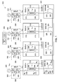
Fig. 1 is a diagram of an exemplary ring bus architecture. -
Fig. 2 is a circuit diagram of an exemplary single phase voltage source two level inverter. -
Fig. 3 is a circuit diagram of an exemplary single phase voltage source three level inverter. -
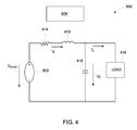
Fig. 4 is a simplified circuit diagram of a single phase inverter. -
Fig. 5 is a block diagram of a voltage control algorithm with current limitation that may be used with the circuit shown inFig. 4 . -
Fig. 6 is a graph illustrating periods of current limiting. -
Fig. 7 is a graph illustrating behavior of a fault current. -
Fig. 8 is a graph illustrating behavior of a fault current when a hybrid voltage/current control algorithm is utilized. - The systems and methods described herein utilize a hybrid voltage/current limiting control. Specifically, utilizing the hybrid voltage/current limiting control described herein, it is possible to quickly re-center a fault current, permitting reducing (e.g., halving) the size of a choke as compared to other approaches. The current limiting control takes over as soon as a predetermined bridge current limit is reached. As a result, the voltage briefly drops, re-centering a fault current and substantially eliminating a large DC fault current that would otherwise occur.
- Exemplary embodiments of an uninterruptible power supply system are described here. A plurality of uninterruptible power supplies are arranged in a ring bus configuration and configured to supply power to at least one load. At least one control device is communicatively coupled to the plurality of uninterruptible power supplies.
-
Fig. 1 is a schematic diagram of an exemplary redundant isolated-parallel (IP) uninterruptible power supply (UPS)ring bus architecture 300. In the exemplary embodiment,architecture 300 includes a plurality ofUPSs 302 arranged in a ring architecture, or parallel architecture, as described herein. Specifically,architecture 300 includes fourUPSs 302 in the exemplary embodiment. Alternatively,architecture 300 may include any number of UPSs 302 that enablearchitecture 300 to function as described herein. In the exemplary embodiment,architecture 300 is a three wire system. Alternatively,architecture 300 may be a four wire system (typically to supply loads that require a neutral wire). - In the exemplary embodiment, UPSs 302 are static double conversion UPSs (i.e., true on-line system systems). Both static and rotary UPSs may require droop control techniques for both voltage and frequency. In some cases, droop control for frequency alone may be sufficient. In some embodiments, droop control techniques are modified in order to handle non-linear loads.
-
Architecture 300 facilitates providing power to one ormore loads 304. Under normal operation, one or more utilities function as avoltage source 303 and provide power alternating current (AC) power to loads 304. Generators may also function asvoltage sources 303. Notably,voltage sources 303 do not need to be synchronized inarchitecture 300. This is advantageous, as every UPS 302 may be fed by an individual generator and/or utility, and there is no need to add additional equipment to synchronizevoltage sources 303. - In the event of a failure of
voltage source 303 or of the UPS rectifier, UPS 302 utilizes energy storage systems 358 (e.g., batteries, flywheels, etc. with their converter) connected toUPSs 302 to keep power flowing to loads 304, as described herein. Further, if a given UPS 302 fails,loads 304 are fed power through aring bus 306, as described herein. In the exemplary embodiment,architecture 300 includes fourloads 304. Alternatively,architecture 300 may include any suitable number ofloads 304 that enablearchitecture 300 to function as described herein. - In the exemplary embodiment, each UPS 302 is electrically coupled to an associated
load 304, and coupled toring bus 306 through an associated choke 308 (e.g., an inductor). Inarchitecture 300, without proper synchronization,UPSs 302 cannot work properly due to undesirable circulation currents. Accordingly, in the exemplary embodiment, at least onecontroller 309 controls operation of UPSs 302. More specifically, at least onecontroller 309 controls a frequency of an output voltage of eachUPS 302, as described herein. The frequency for each UPS 302 is calculated as a function of power, as described herein. - In some embodiments,
architecture 300 includes a separate,dedicated controller 309 for each UPS 302. Alternatively, system may include asingle controller 309 that controls operation of all UPSs 302. Eachcontroller 309 may include its own power system (not shown) such as a dedicated energy source (e.g., a battery). In some embodiments, eachcontroller 309 is coupled to a substitute controller (not shown) that may be used in the event that controller 309 fails. - In the exemplary embodiment, each
controller 309 is implemented by aprocessor 311 communicatively coupled to amemory device 313 for executing instructions. In some embodiments, executable instructions are stored inmemory device 313. Alternatively,controller 309 may be implemented using any circuitry that enablescontroller 309 to control operation ofUPSs 302 as described herein. For example, in some embodiments,controller 309 may include a state machine that learns or is preprogrammed to determine information relevant to which loads 304 require power. - In the exemplary embodiment,
controller 309 performs one or more operations described herein byprogramming processor 311. For example,processor 311 may be programmed by encoding an operation as one or more executable instructions and by providing the executable instructions inmemory device 313.Processor 311 may include one or more processing units (e.g., in a multi-core configuration). Further,processor 311 may be implemented using one or more heterogeneous processor systems in which a main processor is present with secondary processors on a single chip. As another illustrative example,processor 311 may be a symmetric multiprocessor system containing multiple processors of the same type. Further,processor 311 may be implemented using any suitable programmable circuit including one or more systems and microcontrollers, microprocessors, reduced instruction set circuits (RISC), application specific integrated circuits (ASIC), programmable logic circuits, field programmable gate arrays (FPGA), and any other circuit capable of executing the functions described herein. In the exemplary embodiment,processor 311 causescontroller 309 to operateUPSs 302, as described herein. - In the exemplary embodiment,
memory device 313 is one or more devices that enable information such as executable instructions and/or other data to be stored and retrieved.Memory device 313 may include one or more computer readable media, such as, without limitation, dynamic random access memory (DRAM), static random access memory (SRAM), a solid state disk, and/or a hard disk.Memory device 313 may be configured to store, without limitation, application source code, application object code, source code portions of interest, object code portions of interest, configuration data, execution events and/or any other type of data. - In the exemplary embodiment, as described in more detail below, one or
more controllers 309, and more specificallyprocessor 311, calculates an output voltage frequency for eachUPS 302, and one ormore controllers 309 operate eachUPS 302 at the calculated frequency. Operating eachUPS 302 at their respective calculated frequencies as determined by the droop controls makes it possible to achieve load sharing and stability inarchitecture 300. The frequencies of operation across thevarious UPSs 302 are different in transient conditions (e.g., following a variation of one or more loads 304). Once the droop controls are in steady state, allUPSs 302 operate at the same frequency but with a phase shift acrosschokes 308 that equalizes the active power provided by eachUPS 302. - In
architecture 300, eachUPS 302 is able to supply power to an associatedlocal load 304, as well as transfer active and reactive power to ringbus 306 through an associatedchoke 308. In the exemplary embodiment,architecture 300 facilitates sharinglocal loads 304 equally betweenUPSs 302 without any communication using droop controls, and in particular, frequency versus active power and voltage versus reactive power. This removes limitations on the number ofUPSs 302 inarchitecture 300. - In the exemplary embodiment,
architecture 300 includes a number of circuit breakers. Specifically, for eachUPS 302, afirst circuit breaker 310 is electrically coupled betweenUPS 302 and choke 308, asecond circuit breaker 312 is electrically coupled betweenfirst circuit breaker 310 andlocal load 304, athird circuit breaker 314 is electrically coupled betweenfirst circuit breaker 310 andring bus 306, and afourth circuit breaker 316 is coupled betweenchoke 308 andring bus 306. Further, atring bus 306, acentral circuit breaker 320, aleft circuit breaker 322, and aright circuit breaker 324 are associated with eachUPS 302, and facilitate isolatingUPS 302 fromring bus 306 and/orother UPSs 302 onring bus 306. Eachcircuit breaker circuit breakers architecture 300 and isolating those faults by opening the appropriate breakers. Further,third circuit breakers 314, also referred to as bypass breakers, facilitate bypassingchoke 308 when the associatedUPS 302 fails or is under maintenance. This facilitates improving the quality of the voltage on the associatedlocal load 304 as the voltage drop onchoke 308 is removed. - For ring bus applications, chokes 308 are sized to sustain a bolted fault on
ring bus 306 for a long enough time to guarantee isolation of the fault through the activation of the specific breakers inarchitecture 300. Further, for situations where a breaker fails to open, additional time should be built-in to determine and execute an alternative fault isolation strategy. Accordingly, to facilitate maximizing a duration of time where the inverter in an associatedUPS 302 can sustain a bolted fault onring bus 306, chokes 308 may be sized to operate the inverter in a linear mode under a short circuit onring bus 306. The systems and methods described herein facilitate a rapid elimination of the DC fault current component, as described herein. Accordingly, the size ofchokes 308 may be reduced proportionally. - As shown in
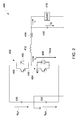
Fig. 1 , eachUPS 302 includes aninverter 330. Different designs are possible forinverters 330. For example, for transformerless designs,Fig. 2 is a circuit diagram of an exemplary single phase voltage source twolevel inverter 400, andFig. 3 is a circuit diagram of an exemplary single phase voltage source threelevel inverter 500. - As shown in
Fig. 2 ,inverter 400 includes afirst switching device 402 and asecond switching device 404.First switching device 402 includes a first switch 405 (e.g., a transistor) electrically coupled in parallel with afirst diode 406, andsecond switching device 404 includes a second switch 407 (e.g., a transistor) electrically coupled in parallel with asecond diode 408. A voltage across the lower, orsecond switching device 404 is referred to herein as a command voltage, ucmd. Anode 410 between first andsecond switching devices inductor 412 and aresistor 414. Bridge current is splits into a load current, iL, that flows to load 416 (such as local load 304) and a current that flows through acapacitor 418. The total load current is the sum of load current iL and a potential fault current. A voltage acrosscapacitor 418 is referred to as a capacitor voltage, uC.Inverter 400 includes afirst DC capacitor 430 electrically coupled betweenfirst switching device 402 and neutral 420, and asecond DC capacitor 432 electrically coupled betweensecond switching device 404 and neutral 420. The voltage acrossfirst DC capacitor 430 is an upper DC link voltage, VdcP, and the voltage acrosssecond DC capacitor 432 is a lower DC link voltage, VdcN. - Unless indicated otherwise,
inverter 500 is substantially similar toinverter 400. As shown inFig. 3 ,inverter 500 includes athird switching device 502 and afourth switching device 504 electrically coupled in series betweennode 410 and neutral 420.Third switching device 502 includes a third switch 505 (e.g., a transistor) electrically coupled in parallel with athird diode 506, andfourth switching device 504 includes a fourth switch 507 (e.g., a transistor) electrically coupled in parallel with afourth diode 508. Third andfourth switching devices inverter 400 andinverter 500 may be implemented as three phase converters by using three legs. - For both
inverter 400 andinverter 500,Fig. 4 is a circuit diagram of theequivalent circuit 600 of a single phase inverter.Circuit 600 includes the command voltage ucmd represented as avoltage source 602. The discontinuous command voltage ucmd models the two or three level inverter. Hence, this voltage may have square wave variations between two or three possible values. In the exemplary embodiment, acontroller 604, such as controller 309 (shown inFig. 1 ), controls operation of one or more components ofcircuit 600. -
Fig. 5 is a block diagram 700 of an exemplary voltage control algorithm with current limitation that may be used withcircuit 600. The steps of block diagram 700 may be performed, for example, using controller 604 (shown inFig. 4 ). In block diagram 700, avoltage controller block 702, Ru, implements and determines the command voltage ucmd based on a reference voltage, uref, a quadrature reference voltage, urefQ, the capacitor voltage uc, the load current iL and the bridge current is. The reference voltage uref and quadrature reference voltage urefQ may be predetermined values stored in a memory, such as memory device 313 (shown inFig. 1 ). Alternatively, the reference voltage uref and quadrature reference voltage urefQ may be computed using equations, for example, in the following manner: uref = A*sin(2*π*f*time) and urefQ = B*cos(2*π*f*time). - A
modulation block 704, M, implements modulation that determines gating signals di for power switches (e.g., gating signals d1 and d2 for first andsecond switches inverter 400, and gating signals d1 ... d4 for first, second, third, andfourth switches limitation block 706, Lis, implements a bridge current limitation that can modify the gating signals di for the power switches. In the exemplary embodiment, limitation block 706 uses a hysteresis comparator to check if the bridge current is exceeds a predefined current limit, Ismax. - In particular, considering a positive current, when the bridge current is exceeds the limit Ismax, the gating signals di for the switches are modified in such a way to make the current is decrease. This depends on the topology of the inverter used. As an example, consider
inverter 400 ofFig. 2 . For a positive and increasing current is,first switch 405 is closed andsecond switch 407 is open. If the current is exceeds the limit Ismax,first switch 405 is commanded to open bylimitation block 706. As a result, the current is will flow throughsecond diode 408 and will decrease as the LC filter formed byinductor 412 andcapacitor 418 is reverse biased. When the current falls below a lower maximal limit IsmaxLOW (e.g., approximately 70% of Ismax),voltage control block 702 andmodulation block 704 take over the control again. Control is performed similarly for a negative current, by operating switches to cause the negative bridge current is to increase (i.e., move towards zero current) once the negative bridge current is falls below a limit -Ismax. -
Limitation block 706 can implement additional features to improve performance in embodiments including a three level inverter (e.g., inverter 500). For example, ininverter 500, the bi-directional switching device formed by third andfourth switching devices limitation block 706 in order to commutate the command voltage Ucmd from VdcP to 0 and then -VdcN. This reduces commutation overvoltage on the switches. - In block diagram 700, a
system block 708, S, represents the controlled system, in particular the inverter bridge and the LC filter (seeFigs. 2-4 ). For a three phase system, a three phase inverter may be used in combination with adifferent controller 604 for every phase. Alternatively, the current limiting strategy described herein may be implemented using a space vector approach. - This operation of block diagram 700 is illustrated in
Fig. 6 , which is agraph 800 that illustrates periods of current limiting when slim = 1. The current limiting operation of block diagram 700 may be controlled by a timer mechanism implemented usingcontroller 604 that triggers when the current limit Ismax is first hit and then checks the duration against a defined limit (e.g., 100 milliseconds (ms)). To facilitate optimizing the design of inverters inarchitecture 300, the current limit may be set slightly above the typical maximum 150% overload capability of the inverters that can usually be sustained for 30 seconds (s). - Referring back to
Fig. 1 , to facilitate maximizing a duration of time where aninverter 330 in an associatedUPS 302 can sustain a bolted fault onring bus 306, chokes 308 are typically sized to operateinverter 330 in a linear mode under a short circuit onring bus 306. -
Fig. 7 is agraph 900 illustrating behavior of a fault current without implementing the hybrid voltage/current control algorithm shown inFig. 5 .Graph 900 includes an inductive faultcurrent curve 902 and avoltage curve 904 plotted over time during a bolted fault onring bus 306. As shown inFig. 7 , depending on a phase angle of the short circuit onring bus 306, an inductive fault current throughchoke 308 can include a relatively large DC component (see, e.g., the initial dip in inductive fault current curve 902). This DC component decays over time to "re-center" with an L/R time constant ofchoke 308. As shown inFig. 7 , inductive faultcurrent curve 902 recenters relatively slowly. Accordingly, a transient peak fault current may reach twice a steady state fault current (see, e.g., the initial dip in inductive fault current curve 902). - To keep
inverter 330 ofUPS 302 operating in a linear mode of operation, one approach is to increase (e.g., double) the size ofchokes 308. This may be impractical, as static UPSs, such asUPSs 302, have a limited fault current capability that may demand a relatively large choke. - However, using the hybrid voltage/current control algorithm described herein, it is possible to re-center a fault current relatively quickly, typically in a fraction of a cycle. For example, in
Fig. 8 , a re-centering time is approximately ¼ of a cycle. Accordingly, the size ofchoke 308 may be kept relatively small. Specifically, as described above in reference toFig. 7 , a current limiting control is utilized when a maximum bridge current limit, ±Ismax, is reached. As a result, the voltage briefly drops (in absolute value), quickly re-centering the fault current. - For example,
Fig. 8 is agraph 1000 illustrating behavior of a fault current while implementing the hybrid voltage/current control algorithm shown inFig. 5 .Graph 1000 includes an inductive faultcurrent curve 1002 and avoltage curve 1004 plotted over time during a bolted fault onring bus 306. As shown in Fig. 10, once the bridge current is (seeFigs. 2 and3 ) reaches the lower threshold -Ismax, the hybrid voltage/current control algorithm causesvoltage curve 1004 to briefly drop, resulting in a relatively quick re-centering of inductive faultcurrent curve 1002. With reference toFigs. 4 and8 , in the case of a bolted fault onring bus 306,load 416 ischoke 308, inductive faultcurrent curve 1002 is the load current iL, andvoltage curve 1004 is the capacitor voltage uc. - In conclusion, utilizing the hybrid voltage/current limiting control described herein, it is possible to quickly re-center the fault current, permitting reducing (e.g., halving) the size of the choke as compared to other approaches. The current limiting control takes over as soon as a predetermined bridge current limit is reached. As a result, the voltage briefly drops (in absolute value), re-centering the fault current and substantially eliminating the large DC fault current that would otherwise occur.
- The systems and methods described herein are applicable independent of voltage level, and more particularly, are applicable to both low voltage (LV) (e.g., 480V phase-phase) and medium voltage (MV) (e.g., 13.8kV phase-phase) applications. For example, although the inverter topologies described herein are typically used in LV systems, the principles of the embodiments described herein can be equally applied to MV systems using appropriate inverter technologies.
- As compared to at least some known power systems, the systems and methods described herein facilitate reducing relatively large DC fault currents. Specifically, a control device determines when a bridge current in an inverter reaches a predetermined bridge current limit, and implements, in response to the determination, a hybrid voltage/current limiting control algorithm that modifies a capacitor voltage in the inverter to reduce a DC fault current component of a load current in the inverter.
- Exemplary embodiments of systems and methods for uninterruptible power supplies are described above in detail. The systems and methods are not limited to the specific embodiments described herein but, rather, components of the systems and/or operations of the methods may be utilized independently and separately from other components and/or operations described herein. Further, the described components and/or operations may also be defined in, or used in combination with, other systems, methods, and/or devices, and are not limited to practice with only the systems described herein.
- At least one technical effect of the systems and methods described herein includes (a) determining when a bridge current in an inverter of one UPS of a plurality of UPSs reaches a predetermined bridge current limit; and (b) modifying, in response to the determination, a capacitor voltage in the inverter to reduce a DC fault current component of a load current in the inverter.
- The order of execution or performance of the operations in the embodiments of the invention illustrated and described herein is not essential, unless otherwise specified. That is, the operations may be performed in any order, unless otherwise specified, and embodiments of the invention may include additional or fewer operations than those disclosed herein. For example, it is contemplated that executing or performing a particular operation before, contemporaneously with, or after another operation is within the scope of aspects of the invention.
- Although specific features of various embodiments of the invention may be shown in some drawings and not in others, this is for convenience only. In accordance with the principles of the invention, any feature of a drawing may be referenced and/or claimed in combination with any feature of any other drawing.
- This written description uses examples to disclose the invention, including the best mode, and also to enable any person skilled in the art to practice the invention, including making and using any devices or systems and performing any incorporated methods. The patentable scope of the invention is defined by the claims, and may include other examples that occur to those skilled in the art. Such other examples are intended to be within the scope of the claims if they have structural elements that do not differ from the literal language of the claims, or if they include equivalent structural elements with insubstantial differences from the literal language of the claims.
Claims (14)
- At least one controller (309) for controlling a power supply system (300) that includes a plurality of uninterruptible power supplies (UPSs) (302), a ring bus (306), and at least one load (304) electrically coupled to the plurality of UPSs and the ring bus, said at least one controller comprising:a processor (311); anda memory device (313) communicatively coupled to said processor, said memory device storing executable instructions configured to cause said processor to:determine when a bridge current in an inverter (330) of at least one UPS of the plurality of UPSs reaches a predetermined bridge current limit; andmodify a capacitor voltage in the inverter to reduce a DC fault current component of a load current in the inverter.
- At least one controller (309) in accordance with Claim 1, wherein to modify a capacitor voltage, said at least one controller is configured to implement a control algorithm that modifies gating signals for switches (405, 407) in the inverter (330) when the bridge current reaches the predefined current limit.
- At least one controller (309) in accordance with Claim 2, wherein to implement a control algorithm, said at least one controller (309) is configured to implement a control algorithm that modifies gating signals such that a magnitude of the bridge current decreases.
- A system (300) comprising:a plurality of uninterruptible power supplies (UPSs) (302), each UPS of the plurality of UPSs comprising an inverter (330);a ring bus (306); andat least one controller (309) communicatively coupled to said plurality of UPSs, said at least one controller as recited in any of claims 1 to 3.
- A system (300) in accordance with Claim 4, wherein said inverter (330) comprises a single phase voltage source two level inverter (400).
- A system (300) in accordance with Claim 4, wherein said inverter (330) comprises a single phase voltage source three level inverter (500).
- A system (300) in accordance with any of Claims 4 to 6, wherein the load current is a sum of at least one of a current through a load (304) associated with the at least one UPS (302) and a fault current in the at least one UPS.
- A system (300) in accordance with any of Claims 4 to 7, further comprising at least one circuit breaker (310) coupled between said at least one UPS (302) and said ring bus (306).
- A method of controlling a power supply system that includes a plurality of uninterruptible power supplies (UPSs), a ring bus, and at least one load electrically coupled to the plurality of UPSs and the ring bus, the method comprising:determining when a bridge current in an inverter of at least one UPS of the plurality of UPSs reaches a predetermined bridge current limit; andmodifying, in response to the determination, a capacitor voltage in the inverter to reduce a DC fault current component of a load current in the inverter.
- A method in accordance with Claim 9, wherein modifying a capacitor voltage comprises implementing a control algorithm that modifies gating signals for switches in the inverter when the bridge current reaches the predefined current limit.
- A method in accordance with Claim 10, wherein implementing a control algorithm comprises implementing a control algorithm that modifies gating signals such that a magnitude of the bridge current decreases.
- A method in accordance with any of Claim 9 or 10, wherein modifying a capacitor voltage comprises modifying a capacitor voltage in a single phase voltage source three level inverter.
- A method in accordance with any of Claims 9 to 11, wherein modifying a capacitor voltage comprises modifying a capacitor voltage in a single phase voltage source two level inverter.
- A method in accordance with any of Claims 9 to 13, wherein modifying a capacitor voltage comprises implementing a control algorithm that reduces a DC fault current component of a load current through a choke associated with the at least one UPS.
Applications Claiming Priority (2)
| Application Number | Priority Date | Filing Date | Title |
|---|---|---|---|
| US201462030843P | 2014-07-30 | 2014-07-30 | |
| US14/568,632 US10608428B2 (en) | 2014-07-30 | 2014-12-12 | Systems and methods for hybrid voltage and current control in static UPS systems |
Publications (2)
| Publication Number | Publication Date |
|---|---|
| EP2980960A1 true EP2980960A1 (en) | 2016-02-03 |
| EP2980960B1 EP2980960B1 (en) | 2020-06-24 |
Family
ID=53546157
Family Applications (1)
| Application Number | Title | Priority Date | Filing Date |
|---|---|---|---|
| EP15176637.5A Active EP2980960B1 (en) | 2014-07-30 | 2015-07-14 | Systems and methods for hybrid voltage and current control in static ups systems |
Country Status (4)
| Country | Link |
|---|---|
| US (1) | US10608428B2 (en) |
| EP (1) | EP2980960B1 (en) |
| CN (1) | CN105322524B (en) |
| ES (1) | ES2815575T3 (en) |
Cited By (1)
| Publication number | Priority date | Publication date | Assignee | Title |
|---|---|---|---|---|
| CN105896722A (en) * | 2016-04-13 | 2016-08-24 | 安徽智瑞电气有限公司 | Intelligent electric power inverter power source system |
Families Citing this family (4)
| Publication number | Priority date | Publication date | Assignee | Title |
|---|---|---|---|---|
| CN108832614B (en) * | 2018-04-23 | 2020-05-19 | 北方工业大学 | Power distribution equipment fault processing method and device based on fuzzy control |
| CN109088395B (en) * | 2018-09-10 | 2020-02-07 | 中国船舶重工集团公司第七0四研究所 | Generator protection device based on closed-loop ship power system |
| CN110729087B (en) * | 2019-10-18 | 2021-10-15 | 大连理工大学 | Voltage-controlled material resistance change curve controllable combination device and implementation method |
| CN112260246B (en) * | 2020-11-09 | 2021-10-26 | 珠海格力电器股份有限公司 | Control method of current limiting control circuit and electrical system |
Citations (4)
| Publication number | Priority date | Publication date | Assignee | Title |
|---|---|---|---|---|
| US5579197A (en) * | 1995-01-24 | 1996-11-26 | Best Power Technology, Incorporated | Backup power system and method |
| US20050036248A1 (en) * | 2003-08-15 | 2005-02-17 | American Power Conversion Corporation | Uninterruptible power supply |
| US20130076142A1 (en) * | 2011-09-28 | 2013-03-28 | Robert William Johnson, Jr. | Ac power supply apparatus and methods providing variable voltage waveforms for load transient conditions |
| WO2013101432A2 (en) * | 2011-12-26 | 2013-07-04 | Schneider Electric It Corporation | System and method for maintaining proper phase neutral wiring in a power system |
Family Cites Families (18)
| Publication number | Priority date | Publication date | Assignee | Title |
|---|---|---|---|---|
| TW245848B (en) | 1991-09-18 | 1995-04-21 | Toshiba Kk | |
| US6122184A (en) * | 1997-06-19 | 2000-09-19 | The Texas A&M University System | Method and system for an improved converter output filter for an induction drive system |
| US6191500B1 (en) | 1998-11-06 | 2001-02-20 | Kling Lindquist Partnership, Inc. | System and method for providing an uninterruptible power supply to a critical load |
| US6630752B2 (en) | 2001-09-12 | 2003-10-07 | Qualmag, Inc. | Uninterruptible transfer switch |
| US20050200205A1 (en) | 2004-01-30 | 2005-09-15 | Winn David W. | On-site power generation system with redundant uninterruptible power supply |
| US7368880B2 (en) * | 2004-07-19 | 2008-05-06 | Intersil Americas Inc. | Phase shift modulation-based control of amplitude of AC voltage output produced by double-ended DC-AC converter circuitry for powering high voltage load such as cold cathode fluorescent lamp |
| EP1890371A1 (en) | 2006-08-03 | 2008-02-20 | Michael J. Mosman | UPS system configuration comprising parallel modules being independent of each other |
| DE102007021089B3 (en) | 2007-05-03 | 2008-12-11 | Piller Power Systems Gmbh | Method for controlling parallel-connected backup power sources and device with parallel-connected backup power sources |
| TWI342652B (en) * | 2008-01-07 | 2011-05-21 | Ablerex Electronics Co Ltd | Ups system having a function of parallel operation |
| CA2740765C (en) * | 2008-10-16 | 2014-12-30 | Toshiba Mitsubishi-Electric Industrial Systems Corporation | Power conversion device |
| WO2012056766A1 (en) * | 2010-10-27 | 2012-05-03 | 三菱電機株式会社 | Power conversion apparatus |
| FR2985616B1 (en) * | 2012-01-09 | 2014-02-14 | Converteam Technology Ltd | REACTIVE ENERGY COMPENSATOR AND METHOD OF BALANCING HALF BUS ASSOCIATED VOLTAGES |
| US9236768B2 (en) | 2012-01-31 | 2016-01-12 | Lorenzo Giuntini | Systems, methods, and devices for control of parallel uninterruptible power supplies |
| US9722459B2 (en) * | 2012-06-12 | 2017-08-01 | Schneider Electric It Corporation | Apparatus and method for providing uninterruptible power |
| US9225262B2 (en) * | 2012-06-29 | 2015-12-29 | Eaton Corporation | Multi-level inverter apparatus and methods using variable overcurrent response |
| US9404947B2 (en) | 2012-08-31 | 2016-08-02 | General Electric Company | Systems and methods for detecting power quality of uninterrupible power supplies |
| US9239364B2 (en) * | 2012-12-18 | 2016-01-19 | Eaton Corporation | Methods of testing unInterruptible power supply (UPS) systems with multiple UPS modules |
| US9831675B2 (en) * | 2012-12-27 | 2017-11-28 | General Electric Company | System for common redundant bypass feed paths in uninterruptible power supplies |
-
2014
- 2014-12-12 US US14/568,632 patent/US10608428B2/en active Active
-
2015
- 2015-07-14 EP EP15176637.5A patent/EP2980960B1/en active Active
- 2015-07-14 ES ES15176637T patent/ES2815575T3/en active Active
- 2015-07-30 CN CN201510457216.5A patent/CN105322524B/en active Active
Patent Citations (4)
| Publication number | Priority date | Publication date | Assignee | Title |
|---|---|---|---|---|
| US5579197A (en) * | 1995-01-24 | 1996-11-26 | Best Power Technology, Incorporated | Backup power system and method |
| US20050036248A1 (en) * | 2003-08-15 | 2005-02-17 | American Power Conversion Corporation | Uninterruptible power supply |
| US20130076142A1 (en) * | 2011-09-28 | 2013-03-28 | Robert William Johnson, Jr. | Ac power supply apparatus and methods providing variable voltage waveforms for load transient conditions |
| WO2013101432A2 (en) * | 2011-12-26 | 2013-07-04 | Schneider Electric It Corporation | System and method for maintaining proper phase neutral wiring in a power system |
Cited By (2)
| Publication number | Priority date | Publication date | Assignee | Title |
|---|---|---|---|---|
| CN105896722A (en) * | 2016-04-13 | 2016-08-24 | 安徽智瑞电气有限公司 | Intelligent electric power inverter power source system |
| CN105896722B (en) * | 2016-04-13 | 2018-09-25 | 安徽智瑞电气有限公司 | Intelligent electric power inverter system |
Also Published As
| Publication number | Publication date |
|---|---|
| CN105322524A (en) | 2016-02-10 |
| ES2815575T3 (en) | 2021-03-30 |
| US20160036215A1 (en) | 2016-02-04 |
| EP2980960B1 (en) | 2020-06-24 |
| CN105322524B (en) | 2020-08-21 |
| US10608428B2 (en) | 2020-03-31 |
Similar Documents
| Publication | Publication Date | Title |
|---|---|---|
| EP2919350B1 (en) | Systems and methods for providing increased fault current capability in uninterruptible power supply systems | |
| US11081903B2 (en) | Protection methods and switches in uninterruptible power supply systems | |
| EP2980960B1 (en) | Systems and methods for hybrid voltage and current control in static ups systems | |
| CN105305532B (en) | System and method for managing backfeed in an uninterruptible power supply system | |
| US9705360B2 (en) | Redundant uninterruptible power supply systems | |
| CN104917277B (en) | Redundant uninterruptible power supply system | |
| US9882424B2 (en) | Redundant uninterruptible power supply systems | |
| CN105720677B (en) | System and method for implementing series compensator in static UPS | |
| CN105006878B (en) | System and method for providing increased fault current capability in an uninterruptible power supply system | |
| EP2980959B1 (en) | Systems and methods for exploiting current capability in static ups | |
| CA2921793A1 (en) | Converter arrangement |
Legal Events
| Date | Code | Title | Description |
|---|---|---|---|
| PUAI | Public reference made under article 153(3) epc to a published international application that has entered the european phase |
Free format text: ORIGINAL CODE: 0009012 |
|
| AK | Designated contracting states |
Kind code of ref document: A1 Designated state(s): AL AT BE BG CH CY CZ DE DK EE ES FI FR GB GR HR HU IE IS IT LI LT LU LV MC MK MT NL NO PL PT RO RS SE SI SK SM TR |
|
| AX | Request for extension of the european patent |
Extension state: BA ME |
|
| 17P | Request for examination filed |
Effective date: 20160803 |
|
| RBV | Designated contracting states (corrected) |
Designated state(s): AL AT BE BG CH CY CZ DE DK EE ES FI FR GB GR HR HU IE IS IT LI LT LU LV MC MK MT NL NO PL PT RO RS SE SI SK SM TR |
|
| STAA | Information on the status of an ep patent application or granted ep patent |
Free format text: STATUS: EXAMINATION IS IN PROGRESS |
|
| 17Q | First examination report despatched |
Effective date: 20180309 |
|
| RAP1 | Party data changed (applicant data changed or rights of an application transferred) |
Owner name: ABB SCHWEIZ AG |
|
| GRAP | Despatch of communication of intention to grant a patent |
Free format text: ORIGINAL CODE: EPIDOSNIGR1 |
|
| STAA | Information on the status of an ep patent application or granted ep patent |
Free format text: STATUS: GRANT OF PATENT IS INTENDED |
|
| INTG | Intention to grant announced |
Effective date: 20200127 |
|
| GRAS | Grant fee paid |
Free format text: ORIGINAL CODE: EPIDOSNIGR3 |
|
| GRAA | (expected) grant |
Free format text: ORIGINAL CODE: 0009210 |
|
| STAA | Information on the status of an ep patent application or granted ep patent |
Free format text: STATUS: THE PATENT HAS BEEN GRANTED |
|
| AK | Designated contracting states |
Kind code of ref document: B1 Designated state(s): AL AT BE BG CH CY CZ DE DK EE ES FI FR GB GR HR HU IE IS IT LI LT LU LV MC MK MT NL NO PL PT RO RS SE SI SK SM TR |
|
| REG | Reference to a national code |
Ref country code: GB Ref legal event code: FG4D |
|
| REG | Reference to a national code |
Ref country code: CH Ref legal event code: EP |
|
| REG | Reference to a national code |
Ref country code: AT Ref legal event code: REF Ref document number: 1284851 Country of ref document: AT Kind code of ref document: T Effective date: 20200715 |
|
| REG | Reference to a national code |
Ref country code: DE Ref legal event code: R096 Ref document number: 602015054628 Country of ref document: DE |
|
| REG | Reference to a national code |
Ref country code: IE Ref legal event code: FG4D |
|
| REG | Reference to a national code |
Ref country code: CH Ref legal event code: NV Representative=s name: CABINET GERMAIN AND MAUREAU, CH |
|
| PG25 | Lapsed in a contracting state [announced via postgrant information from national office to epo] |
Ref country code: FI Free format text: LAPSE BECAUSE OF FAILURE TO SUBMIT A TRANSLATION OF THE DESCRIPTION OR TO PAY THE FEE WITHIN THE PRESCRIBED TIME-LIMIT Effective date: 20200624 Ref country code: SE Free format text: LAPSE BECAUSE OF FAILURE TO SUBMIT A TRANSLATION OF THE DESCRIPTION OR TO PAY THE FEE WITHIN THE PRESCRIBED TIME-LIMIT Effective date: 20200624 Ref country code: NO Free format text: LAPSE BECAUSE OF FAILURE TO SUBMIT A TRANSLATION OF THE DESCRIPTION OR TO PAY THE FEE WITHIN THE PRESCRIBED TIME-LIMIT Effective date: 20200924 Ref country code: GR Free format text: LAPSE BECAUSE OF FAILURE TO SUBMIT A TRANSLATION OF THE DESCRIPTION OR TO PAY THE FEE WITHIN THE PRESCRIBED TIME-LIMIT Effective date: 20200925 Ref country code: LT Free format text: LAPSE BECAUSE OF FAILURE TO SUBMIT A TRANSLATION OF THE DESCRIPTION OR TO PAY THE FEE WITHIN THE PRESCRIBED TIME-LIMIT Effective date: 20200624 |
|
| REG | Reference to a national code |
Ref country code: LT Ref legal event code: MG4D |
|
| PG25 | Lapsed in a contracting state [announced via postgrant information from national office to epo] |
Ref country code: RS Free format text: LAPSE BECAUSE OF FAILURE TO SUBMIT A TRANSLATION OF THE DESCRIPTION OR TO PAY THE FEE WITHIN THE PRESCRIBED TIME-LIMIT Effective date: 20200624 Ref country code: BG Free format text: LAPSE BECAUSE OF FAILURE TO SUBMIT A TRANSLATION OF THE DESCRIPTION OR TO PAY THE FEE WITHIN THE PRESCRIBED TIME-LIMIT Effective date: 20200924 Ref country code: LV Free format text: LAPSE BECAUSE OF FAILURE TO SUBMIT A TRANSLATION OF THE DESCRIPTION OR TO PAY THE FEE WITHIN THE PRESCRIBED TIME-LIMIT Effective date: 20200624 Ref country code: HR Free format text: LAPSE BECAUSE OF FAILURE TO SUBMIT A TRANSLATION OF THE DESCRIPTION OR TO PAY THE FEE WITHIN THE PRESCRIBED TIME-LIMIT Effective date: 20200624 |
|
| REG | Reference to a national code |
Ref country code: NL Ref legal event code: MP Effective date: 20200624 |
|
| REG | Reference to a national code |
Ref country code: AT Ref legal event code: MK05 Ref document number: 1284851 Country of ref document: AT Kind code of ref document: T Effective date: 20200624 |
|
| PG25 | Lapsed in a contracting state [announced via postgrant information from national office to epo] |
Ref country code: AL Free format text: LAPSE BECAUSE OF FAILURE TO SUBMIT A TRANSLATION OF THE DESCRIPTION OR TO PAY THE FEE WITHIN THE PRESCRIBED TIME-LIMIT Effective date: 20200624 Ref country code: NL Free format text: LAPSE BECAUSE OF FAILURE TO SUBMIT A TRANSLATION OF THE DESCRIPTION OR TO PAY THE FEE WITHIN THE PRESCRIBED TIME-LIMIT Effective date: 20200624 |
|
| PG25 | Lapsed in a contracting state [announced via postgrant information from national office to epo] |
Ref country code: SM Free format text: LAPSE BECAUSE OF FAILURE TO SUBMIT A TRANSLATION OF THE DESCRIPTION OR TO PAY THE FEE WITHIN THE PRESCRIBED TIME-LIMIT Effective date: 20200624 Ref country code: EE Free format text: LAPSE BECAUSE OF FAILURE TO SUBMIT A TRANSLATION OF THE DESCRIPTION OR TO PAY THE FEE WITHIN THE PRESCRIBED TIME-LIMIT Effective date: 20200624 Ref country code: AT Free format text: LAPSE BECAUSE OF FAILURE TO SUBMIT A TRANSLATION OF THE DESCRIPTION OR TO PAY THE FEE WITHIN THE PRESCRIBED TIME-LIMIT Effective date: 20200624 Ref country code: CZ Free format text: LAPSE BECAUSE OF FAILURE TO SUBMIT A TRANSLATION OF THE DESCRIPTION OR TO PAY THE FEE WITHIN THE PRESCRIBED TIME-LIMIT Effective date: 20200624 Ref country code: RO Free format text: LAPSE BECAUSE OF FAILURE TO SUBMIT A TRANSLATION OF THE DESCRIPTION OR TO PAY THE FEE WITHIN THE PRESCRIBED TIME-LIMIT Effective date: 20200624 Ref country code: PT Free format text: LAPSE BECAUSE OF FAILURE TO SUBMIT A TRANSLATION OF THE DESCRIPTION OR TO PAY THE FEE WITHIN THE PRESCRIBED TIME-LIMIT Effective date: 20201026 |
|
| PG25 | Lapsed in a contracting state [announced via postgrant information from national office to epo] |
Ref country code: PL Free format text: LAPSE BECAUSE OF FAILURE TO SUBMIT A TRANSLATION OF THE DESCRIPTION OR TO PAY THE FEE WITHIN THE PRESCRIBED TIME-LIMIT Effective date: 20200624 Ref country code: SK Free format text: LAPSE BECAUSE OF FAILURE TO SUBMIT A TRANSLATION OF THE DESCRIPTION OR TO PAY THE FEE WITHIN THE PRESCRIBED TIME-LIMIT Effective date: 20200624 Ref country code: IS Free format text: LAPSE BECAUSE OF FAILURE TO SUBMIT A TRANSLATION OF THE DESCRIPTION OR TO PAY THE FEE WITHIN THE PRESCRIBED TIME-LIMIT Effective date: 20201024 |
|
| REG | Reference to a national code |
Ref country code: DE Ref legal event code: R097 Ref document number: 602015054628 Country of ref document: DE |
|
| REG | Reference to a national code |
Ref country code: ES Ref legal event code: FG2A Ref document number: 2815575 Country of ref document: ES Kind code of ref document: T3 Effective date: 20210330 |
|
| PG25 | Lapsed in a contracting state [announced via postgrant information from national office to epo] |
Ref country code: MC Free format text: LAPSE BECAUSE OF FAILURE TO SUBMIT A TRANSLATION OF THE DESCRIPTION OR TO PAY THE FEE WITHIN THE PRESCRIBED TIME-LIMIT Effective date: 20200624 |
|
| REG | Reference to a national code |
Ref country code: BE Ref legal event code: MM Effective date: 20200731 |
|
| PG25 | Lapsed in a contracting state [announced via postgrant information from national office to epo] |
Ref country code: LU Free format text: LAPSE BECAUSE OF NON-PAYMENT OF DUE FEES Effective date: 20200714 Ref country code: DK Free format text: LAPSE BECAUSE OF FAILURE TO SUBMIT A TRANSLATION OF THE DESCRIPTION OR TO PAY THE FEE WITHIN THE PRESCRIBED TIME-LIMIT Effective date: 20200624 |
|
| PLBE | No opposition filed within time limit |
Free format text: ORIGINAL CODE: 0009261 |
|
| STAA | Information on the status of an ep patent application or granted ep patent |
Free format text: STATUS: NO OPPOSITION FILED WITHIN TIME LIMIT |
|
| PG25 | Lapsed in a contracting state [announced via postgrant information from national office to epo] |
Ref country code: BE Free format text: LAPSE BECAUSE OF NON-PAYMENT OF DUE FEES Effective date: 20200731 |
|
| 26N | No opposition filed |
Effective date: 20210325 |
|
| PG25 | Lapsed in a contracting state [announced via postgrant information from national office to epo] |
Ref country code: SI Free format text: LAPSE BECAUSE OF FAILURE TO SUBMIT A TRANSLATION OF THE DESCRIPTION OR TO PAY THE FEE WITHIN THE PRESCRIBED TIME-LIMIT Effective date: 20200624 Ref country code: IE Free format text: LAPSE BECAUSE OF NON-PAYMENT OF DUE FEES Effective date: 20200714 |
|
| PG25 | Lapsed in a contracting state [announced via postgrant information from national office to epo] |
Ref country code: TR Free format text: LAPSE BECAUSE OF FAILURE TO SUBMIT A TRANSLATION OF THE DESCRIPTION OR TO PAY THE FEE WITHIN THE PRESCRIBED TIME-LIMIT Effective date: 20200624 Ref country code: MT Free format text: LAPSE BECAUSE OF FAILURE TO SUBMIT A TRANSLATION OF THE DESCRIPTION OR TO PAY THE FEE WITHIN THE PRESCRIBED TIME-LIMIT Effective date: 20200624 Ref country code: CY Free format text: LAPSE BECAUSE OF FAILURE TO SUBMIT A TRANSLATION OF THE DESCRIPTION OR TO PAY THE FEE WITHIN THE PRESCRIBED TIME-LIMIT Effective date: 20200624 |
|
| PG25 | Lapsed in a contracting state [announced via postgrant information from national office to epo] |
Ref country code: MK Free format text: LAPSE BECAUSE OF FAILURE TO SUBMIT A TRANSLATION OF THE DESCRIPTION OR TO PAY THE FEE WITHIN THE PRESCRIBED TIME-LIMIT Effective date: 20200624 |
|
| PGFP | Annual fee paid to national office [announced via postgrant information from national office to epo] |
Ref country code: IT Payment date: 20230724 Year of fee payment: 9 Ref country code: GB Payment date: 20230720 Year of fee payment: 9 Ref country code: ES Payment date: 20230926 Year of fee payment: 9 Ref country code: CH Payment date: 20230801 Year of fee payment: 9 |
|
| PGFP | Annual fee paid to national office [announced via postgrant information from national office to epo] |
Ref country code: FR Payment date: 20230726 Year of fee payment: 9 Ref country code: DE Payment date: 20230719 Year of fee payment: 9 |