EP2750194A1 - Light emitting device comprising a plurality of light emitting diode cells - Google Patents
Light emitting device comprising a plurality of light emitting diode cells Download PDFInfo
- Publication number
- EP2750194A1 EP2750194A1 EP20140161338 EP14161338A EP2750194A1 EP 2750194 A1 EP2750194 A1 EP 2750194A1 EP 20140161338 EP20140161338 EP 20140161338 EP 14161338 A EP14161338 A EP 14161338A EP 2750194 A1 EP2750194 A1 EP 2750194A1
- Authority
- EP
- European Patent Office
- Prior art keywords
- light emitting
- semiconductor layer
- type semiconductor
- layer
- emitting device
- Prior art date
- Legal status (The legal status is an assumption and is not a legal conclusion. Google has not performed a legal analysis and makes no representation as to the accuracy of the status listed.)
- Ceased
Links
Images


Classifications
-
- H—ELECTRICITY
- H01—ELECTRIC ELEMENTS
- H01L—SEMICONDUCTOR DEVICES NOT COVERED BY CLASS H10
- H01L27/00—Devices consisting of a plurality of semiconductor or other solid-state components formed in or on a common substrate
- H01L27/15—Devices consisting of a plurality of semiconductor or other solid-state components formed in or on a common substrate including semiconductor components with at least one potential-jump barrier or surface barrier specially adapted for light emission
- H01L27/153—Devices consisting of a plurality of semiconductor or other solid-state components formed in or on a common substrate including semiconductor components with at least one potential-jump barrier or surface barrier specially adapted for light emission in a repetitive configuration, e.g. LED bars
-
- H—ELECTRICITY
- H01—ELECTRIC ELEMENTS
- H01L—SEMICONDUCTOR DEVICES NOT COVERED BY CLASS H10
- H01L33/00—Semiconductor devices with at least one potential-jump barrier or surface barrier specially adapted for light emission; Processes or apparatus specially adapted for the manufacture or treatment thereof or of parts thereof; Details thereof
- H01L33/02—Semiconductor devices with at least one potential-jump barrier or surface barrier specially adapted for light emission; Processes or apparatus specially adapted for the manufacture or treatment thereof or of parts thereof; Details thereof characterised by the semiconductor bodies
- H01L33/08—Semiconductor devices with at least one potential-jump barrier or surface barrier specially adapted for light emission; Processes or apparatus specially adapted for the manufacture or treatment thereof or of parts thereof; Details thereof characterised by the semiconductor bodies with a plurality of light emitting regions, e.g. laterally discontinuous light emitting layer or photoluminescent region integrated within the semiconductor body
-
- H—ELECTRICITY
- H01—ELECTRIC ELEMENTS
- H01L—SEMICONDUCTOR DEVICES NOT COVERED BY CLASS H10
- H01L33/00—Semiconductor devices with at least one potential-jump barrier or surface barrier specially adapted for light emission; Processes or apparatus specially adapted for the manufacture or treatment thereof or of parts thereof; Details thereof
- H01L33/02—Semiconductor devices with at least one potential-jump barrier or surface barrier specially adapted for light emission; Processes or apparatus specially adapted for the manufacture or treatment thereof or of parts thereof; Details thereof characterised by the semiconductor bodies
- H01L33/20—Semiconductor devices with at least one potential-jump barrier or surface barrier specially adapted for light emission; Processes or apparatus specially adapted for the manufacture or treatment thereof or of parts thereof; Details thereof characterised by the semiconductor bodies with a particular shape, e.g. curved or truncated substrate
- H01L33/24—Semiconductor devices with at least one potential-jump barrier or surface barrier specially adapted for light emission; Processes or apparatus specially adapted for the manufacture or treatment thereof or of parts thereof; Details thereof characterised by the semiconductor bodies with a particular shape, e.g. curved or truncated substrate of the light emitting region, e.g. non-planar junction
-
- H—ELECTRICITY
- H01—ELECTRIC ELEMENTS
- H01L—SEMICONDUCTOR DEVICES NOT COVERED BY CLASS H10
- H01L33/00—Semiconductor devices with at least one potential-jump barrier or surface barrier specially adapted for light emission; Processes or apparatus specially adapted for the manufacture or treatment thereof or of parts thereof; Details thereof
- H01L33/02—Semiconductor devices with at least one potential-jump barrier or surface barrier specially adapted for light emission; Processes or apparatus specially adapted for the manufacture or treatment thereof or of parts thereof; Details thereof characterised by the semiconductor bodies
- H01L33/26—Materials of the light emitting region
- H01L33/30—Materials of the light emitting region containing only elements of group III and group V of the periodic system
- H01L33/32—Materials of the light emitting region containing only elements of group III and group V of the periodic system containing nitrogen
-
- H—ELECTRICITY
- H01—ELECTRIC ELEMENTS
- H01L—SEMICONDUCTOR DEVICES NOT COVERED BY CLASS H10
- H01L33/00—Semiconductor devices with at least one potential-jump barrier or surface barrier specially adapted for light emission; Processes or apparatus specially adapted for the manufacture or treatment thereof or of parts thereof; Details thereof
- H01L33/48—Semiconductor devices with at least one potential-jump barrier or surface barrier specially adapted for light emission; Processes or apparatus specially adapted for the manufacture or treatment thereof or of parts thereof; Details thereof characterised by the semiconductor body packages
- H01L33/62—Arrangements for conducting electric current to or from the semiconductor body, e.g. lead-frames, wire-bonds or solder balls
-
- H—ELECTRICITY
- H01—ELECTRIC ELEMENTS
- H01L—SEMICONDUCTOR DEVICES NOT COVERED BY CLASS H10
- H01L2224/00—Indexing scheme for arrangements for connecting or disconnecting semiconductor or solid-state bodies and methods related thereto as covered by H01L24/00
- H01L2224/01—Means for bonding being attached to, or being formed on, the surface to be connected, e.g. chip-to-package, die-attach, "first-level" interconnects; Manufacturing methods related thereto
- H01L2224/42—Wire connectors; Manufacturing methods related thereto
- H01L2224/44—Structure, shape, material or disposition of the wire connectors prior to the connecting process
- H01L2224/45—Structure, shape, material or disposition of the wire connectors prior to the connecting process of an individual wire connector
- H01L2224/45001—Core members of the connector
- H01L2224/45099—Material
- H01L2224/451—Material with a principal constituent of the material being a metal or a metalloid, e.g. boron (B), silicon (Si), germanium (Ge), arsenic (As), antimony (Sb), tellurium (Te) and polonium (Po), and alloys thereof
- H01L2224/45138—Material with a principal constituent of the material being a metal or a metalloid, e.g. boron (B), silicon (Si), germanium (Ge), arsenic (As), antimony (Sb), tellurium (Te) and polonium (Po), and alloys thereof the principal constituent melting at a temperature of greater than or equal to 950°C and less than 1550°C
- H01L2224/45144—Gold (Au) as principal constituent
-
- H—ELECTRICITY
- H01—ELECTRIC ELEMENTS
- H01L—SEMICONDUCTOR DEVICES NOT COVERED BY CLASS H10
- H01L2224/00—Indexing scheme for arrangements for connecting or disconnecting semiconductor or solid-state bodies and methods related thereto as covered by H01L24/00
- H01L2224/01—Means for bonding being attached to, or being formed on, the surface to be connected, e.g. chip-to-package, die-attach, "first-level" interconnects; Manufacturing methods related thereto
- H01L2224/42—Wire connectors; Manufacturing methods related thereto
- H01L2224/47—Structure, shape, material or disposition of the wire connectors after the connecting process
- H01L2224/48—Structure, shape, material or disposition of the wire connectors after the connecting process of an individual wire connector
- H01L2224/4805—Shape
- H01L2224/4809—Loop shape
- H01L2224/48095—Kinked
-
- H—ELECTRICITY
- H01—ELECTRIC ELEMENTS
- H01L—SEMICONDUCTOR DEVICES NOT COVERED BY CLASS H10
- H01L2224/00—Indexing scheme for arrangements for connecting or disconnecting semiconductor or solid-state bodies and methods related thereto as covered by H01L24/00
- H01L2224/01—Means for bonding being attached to, or being formed on, the surface to be connected, e.g. chip-to-package, die-attach, "first-level" interconnects; Manufacturing methods related thereto
- H01L2224/42—Wire connectors; Manufacturing methods related thereto
- H01L2224/47—Structure, shape, material or disposition of the wire connectors after the connecting process
- H01L2224/48—Structure, shape, material or disposition of the wire connectors after the connecting process of an individual wire connector
- H01L2224/481—Disposition
- H01L2224/48135—Connecting between different semiconductor or solid-state bodies, i.e. chip-to-chip
- H01L2224/48137—Connecting between different semiconductor or solid-state bodies, i.e. chip-to-chip the bodies being arranged next to each other, e.g. on a common substrate
-
- H—ELECTRICITY
- H01—ELECTRIC ELEMENTS
- H01L—SEMICONDUCTOR DEVICES NOT COVERED BY CLASS H10
- H01L2933/00—Details relating to devices covered by the group H01L33/00 but not provided for in its subgroups
- H01L2933/0008—Processes
- H01L2933/0033—Processes relating to semiconductor body packages
- H01L2933/0066—Processes relating to semiconductor body packages relating to arrangements for conducting electric current to or from the semiconductor body
-
- H—ELECTRICITY
- H01—ELECTRIC ELEMENTS
- H01L—SEMICONDUCTOR DEVICES NOT COVERED BY CLASS H10
- H01L33/00—Semiconductor devices with at least one potential-jump barrier or surface barrier specially adapted for light emission; Processes or apparatus specially adapted for the manufacture or treatment thereof or of parts thereof; Details thereof
- H01L33/02—Semiconductor devices with at least one potential-jump barrier or surface barrier specially adapted for light emission; Processes or apparatus specially adapted for the manufacture or treatment thereof or of parts thereof; Details thereof characterised by the semiconductor bodies
- H01L33/20—Semiconductor devices with at least one potential-jump barrier or surface barrier specially adapted for light emission; Processes or apparatus specially adapted for the manufacture or treatment thereof or of parts thereof; Details thereof characterised by the semiconductor bodies with a particular shape, e.g. curved or truncated substrate
-
- H—ELECTRICITY
- H01—ELECTRIC ELEMENTS
- H01L—SEMICONDUCTOR DEVICES NOT COVERED BY CLASS H10
- H01L33/00—Semiconductor devices with at least one potential-jump barrier or surface barrier specially adapted for light emission; Processes or apparatus specially adapted for the manufacture or treatment thereof or of parts thereof; Details thereof
- H01L33/02—Semiconductor devices with at least one potential-jump barrier or surface barrier specially adapted for light emission; Processes or apparatus specially adapted for the manufacture or treatment thereof or of parts thereof; Details thereof characterised by the semiconductor bodies
- H01L33/26—Materials of the light emitting region
- H01L33/28—Materials of the light emitting region containing only elements of group II and group VI of the periodic system
-
- H—ELECTRICITY
- H01—ELECTRIC ELEMENTS
- H01L—SEMICONDUCTOR DEVICES NOT COVERED BY CLASS H10
- H01L33/00—Semiconductor devices with at least one potential-jump barrier or surface barrier specially adapted for light emission; Processes or apparatus specially adapted for the manufacture or treatment thereof or of parts thereof; Details thereof
- H01L33/36—Semiconductor devices with at least one potential-jump barrier or surface barrier specially adapted for light emission; Processes or apparatus specially adapted for the manufacture or treatment thereof or of parts thereof; Details thereof characterised by the electrodes
- H01L33/38—Semiconductor devices with at least one potential-jump barrier or surface barrier specially adapted for light emission; Processes or apparatus specially adapted for the manufacture or treatment thereof or of parts thereof; Details thereof characterised by the electrodes with a particular shape
- H01L33/385—Semiconductor devices with at least one potential-jump barrier or surface barrier specially adapted for light emission; Processes or apparatus specially adapted for the manufacture or treatment thereof or of parts thereof; Details thereof characterised by the electrodes with a particular shape the electrode extending at least partially onto a side surface of the semiconductor body
-
- H—ELECTRICITY
- H01—ELECTRIC ELEMENTS
- H01L—SEMICONDUCTOR DEVICES NOT COVERED BY CLASS H10
- H01L33/00—Semiconductor devices with at least one potential-jump barrier or surface barrier specially adapted for light emission; Processes or apparatus specially adapted for the manufacture or treatment thereof or of parts thereof; Details thereof
- H01L33/44—Semiconductor devices with at least one potential-jump barrier or surface barrier specially adapted for light emission; Processes or apparatus specially adapted for the manufacture or treatment thereof or of parts thereof; Details thereof characterised by the coatings, e.g. passivation layer or anti-reflective coating
-
- H—ELECTRICITY
- H10—SEMICONDUCTOR DEVICES; ELECTRIC SOLID-STATE DEVICES NOT OTHERWISE PROVIDED FOR
- H10K—ORGANIC ELECTRIC SOLID-STATE DEVICES
- H10K50/00—Organic light-emitting devices
- H10K50/80—Constructional details
- H10K50/84—Passivation; Containers; Encapsulations
- H10K50/844—Encapsulations
-
- H—ELECTRICITY
- H10—SEMICONDUCTOR DEVICES; ELECTRIC SOLID-STATE DEVICES NOT OTHERWISE PROVIDED FOR
- H10K—ORGANIC ELECTRIC SOLID-STATE DEVICES
- H10K59/00—Integrated devices, or assemblies of multiple devices, comprising at least one organic light-emitting element covered by group H10K50/00
- H10K59/10—OLED displays
- H10K59/17—Passive-matrix OLED displays
Definitions
- the present invention relates to a light emitting device and a method of manufacturing the same. More particularly, the present invention relates to a nitride based semiconductor light emitting device with enhanced luminous efficiency and brightness and a method of manufacturing the light emitting device.
- a light emitting device refers to an element in which minority carriers (electrons or holes) injected using a p-n junction structure of a semiconductor are produced and certain light is emitted due to recombination of the carriers.
- a light emitting source is formed from any one or combination of compound semiconductor materials such as GaAs, AlGaAs, GaN, InGaN and AlGaInP, so that a variety of colors can be implemented.
- a red light emitting device may be formed from GaAsP or the like; a green light emitting device may be formed from GaP, InGaN or the like; a blue light emitting device may be formed using an InGaN/GaN double hetero structure; and a UV light emitting device may be formed using an AlGaN/GaN or AlGaN/AlGaN structure.
- GaN has a direct bandgap of 3.4eV at a normal temperature and a direct energy bandgap of 1.9eV (InN) to 3.4eV (GaN) or 6.2eV (AlN) by combining with a substance such as InN or AlN.
- GaN is a substance with great applicability to an optical element due to its broad wavelength range from visible light to ultraviolet light. Since the wavelength can be adjusted in such a manner, full-color implementation can be made by means of red, green and blue light emitting devices with a short wavelength range, so that the applicability to a general illumination market as well as a display device market is expected to be greatly increased.
- Light emitting devices have characteristics of lower power consumption, longer lifespan, better installation in a narrow space and stronger resistance against vibration as compared with existing bulbs or fluorescent lamps. Since the light emitting devices are used as display devices and backlights and have superior characteristics in view of the reduction in power consumption and the durability, many studies for applying the light emitting devices to a general illumination field have been recently conducted. In the future, their applicability is expected to extend to a backlight of a large-sized LCD-TV, a vehicle headlight and general illumination. To this end, it is necessary to improve luminous efficiency of light emitting devices, solve a heat dissipation problem, and achieve high brightness and output of the light emitting devices.
- the extraction efficiency is determined as a ratio of electrons injected into the light emitting device to photons emitted to the outside of the light emitting device. That is, the light emitting device becomes bright as the extraction efficiency becomes high. Since the extraction efficiency of the light emitting device is much influenced by the shape and surface pattern of a chip, the structure of a chip and a packaging type, careful attention should be paid when designing the light emitting device.
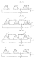
- Fig. 1 is a sectional view showing a conventional light emitting device with a horizontal structure.
- the light emitting device comprises a substrate 1, an N-type semiconductor layer 2 formed on the substrate 1, an active layer 3 formed on a portion of the N-type semiconductor layer 2 and a P-type semiconductor layer 4. That is, after the N-type semiconductor layer 2, the active layer 3 and the P-type semiconductor layer 4 have been sequentially formed on the substrate 1, predetermined regions of the P-type semiconductor layer 4 and the active layer 3 are etched to expose a portion of the N-type semiconductor layer 2. Then, a predetermined voltage is applied to top surfaces of the exposed N-type semiconductor layer 2 and the P-type semiconductor layer 4.
- Fig. 2 is a sectional view showing a conventional light emitting device with a flip chip structure.
- the light emitting device comprises an N-type semiconductor layer 2, an active layer 3 and a P-type semiconductor layer 4, which are sequentially formed on a base substrate 1.
- the light emitting device further comprises a submount substrate 5 onto which the base substrate 1 is flip-chip bonded using metal bumps 8 and 9.
- the N-type semiconductor layer 2, the active layer 3 and the P-type semiconductor layer 4 are sequentially formed on the predetermined substrate 1, and portions of the P-type semiconductor layer 4 and the active layer 3 are etched to expose the N-type semiconductor layer 2 such that a light emitting cell can be formed.
- the additional submount substrate 5 is prepared to form first and second electrodes 6 and 7 thereon, and the P-type and N-type metal bumps 8 and 9 are then formed on the first and second electrodes 6 and 7, respectively.
- the light emitting cell is bonded with the submount substrate 5 such that P and N electrodes of the light emitting cell are bonded with the P-type and N-type metal bumps 8 and 9, respectively, to fabricate a light emitting device. Since such a conventional light emitting device with a flip chip structure has high heat dissipation efficiency and hardly has shield of light, there is an advantage in that its light efficiency is increased by 50% or more as compared with a conventional light emitting device. Further, since a gold wire for driving a light emitting device is not necessary, many applications to a variety of small-sized packages can be considered.
- Light produced from a light emitting layer of a light emitting device is emitted from all the surfaces of a chip, and light extraction efficiency is generally determined by a critical angle of light.
- the conventional light emitting device is etched to expose an N-type semiconductor layer, side surfaces of the P-type semiconductor layer and the active layer are vertically processed such that a portion of light produced within the light emitting device is totally reflected on the etched surface that is processed vertically from a horizontal plane. Then, a considerable amount of light to be totally reflected is not emitted to the outside but dissipated within the light emitting device due to the internal reflection. That is, there is a problem in that luminous efficiency in which electric energy is converted into light energy and the light is then emitted to the outside of a light emitting device is low.
- an object of the present invention is to provide a light emitting device for emitting light with high luminous intensity and brightness by enhancing characteristics of luminous efficiency, external quantum efficiency, extraction efficiency and the like and improving reliability, and a method of manufacturing the light emitting device.
- a light emitting device comprising a plurality of light emitting cells each including an N-type semiconductor layer and a P-type semiconductor layer formed on a portion of the N-type semiconductor layer on a substrate.
- the N-type semiconductor layer of one light emitting cell and the P-type semiconductor layer of another adjacent light emitting cell may be connected to each other, and a side surface including the N-type or P-type semiconductor layer of the light emitting cell has a slope of 20 to 80°from a horizontal plane.
- the light emitting device may further comprise a wire for connecting the N-type semiconductor layer of one light emitting cell and the P-type semiconductor layer of another adjacent light emitting cell, a transparent electrode layer on the P-type semiconductor layer, and P-type and N-type ohmic metal layers containing Cr or Au on the P-type and N-type semiconductor layers, respectively.
- a light emitting device comprising a substrate formed with a plurality of light emitting cells each including an N-type semiconductor layer and a P-type semiconductor layer formed on the N-type semiconductor layer and a submount substrate flip-chip bonded onto the substrate.
- the N-type semiconductor layer of one light emitting cell and the P-type semiconductor layer of another adjacent light emitting cell are connected to each other, and a side surface including at least the P-type semiconductor layer of the light emitting cell has a slope of 20 to 80°from a horizontal plane.
- the light emitting device may further comprise a wire for connecting the N-type semi-conductor layer of one light emitting cell and the P-type semiconductor layer of another adjacent light emitting cell.
- a method of manufacturing a light emitting device comprising the steps of sequentially forming N-type and P-type semiconductor layers on a substrate; forming an etching mask pattern, of which side surface is not perpendicular to but inclined at a predetermined slope from a horizontal plane, on the P-type semiconductor layer; and removing the etching mask pattern and the P-type semiconductor layer exposed through the etching mask pattern.
- a method of manufacturing a light emitting device comprising the steps of removing a portion of the N-type semiconductor layer exposed due to the removal of the P-type semiconductor layer to form a plurality of light emitting cells; and connecting the N-type semiconductor layer of one light emitting cell and the P-type semiconductor layer of another adjacent light emitting cell through a conductive wire.
- a method of manufacturing a light emitting device comprising the step of flip-chip bonding the substrate onto an additional submount substrate after the step of removing the P-type semiconductor layer and the etching mask pattern.
- the method of manufacturing a light emitting device may further comprise the steps of removing a portion of the N-type semiconductor layer exposed through the removal of the P-type semiconductor layer to form a plurality of light emitting cell; and connecting the N-type semiconductor layer of one light emitting cell and the P-type semiconductor layer of another adjacent light emitting cell through a conductive wire, after the step of removing the P-type semiconductor layer and the etching mask pattern.
- the step of forming the plurality of light emitting cells may comprise the steps of forming an etching mask pattern, of which side surface is not perpendicular to but inclined at a predetermined slope from a horizontal plane, on the P-type semiconductor layer; removing the N-type and P-type semiconductor layers exposed through the etching mask pattern to form a plurality of light emitting cells; and removing the etching mask pattern.
- the N type semiconductor layer of one light emitting cell and the P type semiconductor layer of another adjacent light emitting cell may be connected with the conductive wire through a bridge or step coverage process.
- a photoresist with a thickness of 3 to 50 ⁇ may be used in the step of forming the etching mask pattern.
- the step of forming the etching mask pattern may comprise the steps of: applying the photoresist onto the P-type semiconductor layer; light exposing the photoresist in accordance with a predetermined mask pattern; and developing the light-exposed photoresist without a baking process after the light exposure.
- the step of forming the etching mask pattern may comprise the steps of: applying the photoresist onto the P-type semiconductor layer; light exposing the photoresist in accordance with a predetermined mask pattern; hard baking the light-exposed photoresist at a temperature of 100 to 140°C; and developing the hard-baked photoresist.
- the method of manufacturing a light emitting device may further comprise the steps of removing a rear surface of the substrate at a certain thickness; and depositing Al, Ti, Ag, W, Ta, Ni, Ru or an alloy thereof onto the rear surface of the substrate.
- a light emitting device and a method of manufacturing the same In a light emitting device and a method of manufacturing the same according to the present invention, light produced from a side surface of a semiconductor layer, which is not perpendicular to but inclined at a predetermined slop from a horizontal plane, is not totally reflected but emitted to the outside of the light emitting device. Therefore, more enhanced characteristics of light extraction efficiency, external quantum efficiency, luminous efficiency or the like can be obtained. Further, a light emitting device of the present invention emits light with high luminous intensity and brightness and can be applied to a variety of products in which a superior light characteristic is necessary.
- Fig. 3 is a conceptual sectional view illustrating a light emitting device with a horizontal structure according to the present invention.
- the light emitting device comprises a substrate 10, and an N-type semiconductor layer 20, an active layer 30 and a P-type semiconductor layer 40, which are sequentially formed on the substrate 10.
- Each of side surfaces of the P-type semiconductor layer 40, the active layer 30 and a portion of the N-type semiconductor layer 20 has a slope of 80 to 20° from a horizontal plane such that a critical angle of light can be changed by such surfaces and light can be easily extracted. Therefore, luminous efficiency of a light emitting device can be improved.
- Figs. 4 and 5 are sectional views illustrating a process of manufacturing a light emitting device according to a first embodiment of the present invention.
- an N-type semiconductor layer 20, an active layer 30 and a P-type semiconductor layer 40 are sequentially formed on a substrate 10.
- the substrate 10 refers to a general wafer used for fabricating a light emitting device and is made of at least any one of Al 2 O 3 , SiC, ZnO, Si, GaAs, GaP, LiAl 2 O 3 , BN, AlN and GaN.
- a crystal growth substrate made of sapphire is used.
- a buffer layer (not shown) may be further formed on the substrate 10 to reduce lattice mismatch between the substrate 10 and the subsequent layers upon growth of crystals.
- the buffer layer may contain GaN or AlN that is a semiconductor material.
- the N-type semiconductor layer 20 is a layer in which electrons are produced and is preferably made from GaN doped with N-type impurities. However, the N-type semiconductor layer 20 is not limited thereto but may use a material layer having a variety of semiconductor properties.
- the N-type semiconductor layer 20 including N-type Al x Ga 1-x N(0 ⁇ x ⁇ 1) is formed in this embodiment.
- the P-type semiconductor layer 40 is a layer in which holes are produced and is preferably made from GaN doped with P-type impurities. However, the P-type semiconductor layer 40 is not limited thereto but may use a material layer with a variety of semiconductor properties.
- the P-type semiconductor layer 40 including P-type Al x Ga 1-x N(0 ⁇ x ⁇ 1) is formed in this embodiment.
- InGaN may be used as the semiconductor layer.
- each of the N-type and P-type semiconductor layers 20 and 40 may be formed as a multiple layer.
- the active layer 30 has a predetermined bandgap and is a region where a quantum well is formed so that electrons and holes are recombined.
- the active layer 30 may contain InGaN.
- the wavelength of light emitted through the combination of electrons and holes varies according to the kind of a material constituting the active layer 30. Therefore, it is preferred that a semiconductor material contained in the active layer 30 be controlled depending on a target wavelength.
- the aforementioned material layers are formed through a variety of deposition and growth methods including MOCVD (Metal Organic Chemical Vapor Deposition), CVD (Chemical Vapor Deposition), PCVD (Plasma-enhanced Chemical Vapor Deposition), MBE (Molecular Beam Epitaxy), HVPE (Hybride Vapor Phase Epitaxy) and the like.
- MOCVD Metal Organic Chemical Vapor Deposition
- CVD Chemical Vapor Deposition
- PCVD Physical Vapor Deposition
- MBE Molecular Beam Epitaxy
- HVPE Hybride Vapor Phase Epitaxy
- portions of the P-type semiconductor layer 40 and the active layer 30 are removed through a predetermined etching process to expose a portion of the N-type semiconductor layer 20.
- An etching mask pattern is formed on the P-type semiconductor layer 40, and the P-type semiconductor layer 40 and the active layer 30 are then removed through a dry or wet etching process to expose the N-type semiconductor layer 20.
- a photoresist has been applied onto a top surface of the P-type semiconductor layer 40 at a thickness of 1 to 2 ⁇ , and then soft-baked at a temperature of 80 to 90°C is performed.
- an exposure process in which light in a UV range is irradiated through a predetermined photo mask to transfer a pattern formed on the mask to the applied photoresist is executed.
- the photoresist is hard-baked at a temperature of 100 to 120°C, and a developing process in which the photoresist at a portion with relatively weak combination through the exposure process is melted using a solvent is executed.
- a predetermined etching mask pattern is formed on the P-type semiconductor layer 40 through the above process.
- the photoresist is applied at a thickness of 3 to 50 ⁇ which is thicker as compared with the prior art when the etching mask pattern is formed, and the exposure process is performed after the soft-baking.
- a developed side surface of the remaining photoresist is formed into an inclined surface not perpendicular (90°) to but inclined at a predetermined slope from a horizontal plane.
- the side surfaces of the etched P-type semiconductor layer 40, active layer 30 and N-type semiconductor layer 20 can be similarly formed into an inclined surface not perpendicular (90°) to but inclined at a predetermined slope from the horizontal plane.
- a developed etching mask pattern is immediately formed without the hard-baking.
- the P-type semiconductor layer 40 and the active layer 30, which are exposed through the etching mask pattern, are removed through an ICP (Inductive Coupled Plasma) or dry etching process to expose the N-type semiconductor layer 20. A portion of the exposed N-type semiconductor layer 20 may be further removed.
- ICP Inductive Coupled Plasma
- a light emitting device in which the side surfaces of the P-type semiconductor layer 40, the active layer 30 and a portion of the N-type semiconductor layer 20 are not perpendicular (90°) to but inclined at the predetermined slope from a horizontal plane can be manufactured as shown in Fig. 5 .
- hard-baking may be performed.
- the photoresist is hard-baked at a temperature of 100 to 140°C and then developed, the side surface of the developed photoresist may be etched to have a slope of 80 to 20° from a horizontal plane.
- an etching mask pattern with a slope of about 80° from the horizontal plane can be obtained, and the side surfaces of the P-type semiconductor layer 40, the active layer 30 and a portion of the N-type semiconductor layer 20 can have a slope of about 80° from the horizontal plane using the etching mask pattern.
- an etching mask pattern with a slope of about 20° from the horizontal plane can be obtained, and the side surfaces of the P-type semiconductor layer 40, the active layer 30 and a portion of the N-type semiconductor layer 20 can have a slope of about 20° from the horizontal plane using the etching mask pattern.
- the etching mask pattern which the photoresist with a thickness of 3 to 500 has been light-exposed and hard-baked at a temperature of 100 to 140°C and then developed in such a manner, can be used such that the side surfaces of the etched the P-type semiconductor layer 40, active layer 30 and predetermined N-type semiconductor layer 20 have a slope of 80 to 20° from a horizontal plane similarly to the etching mask pattern. Then, light produced within a light emitting layer is not totally reflected on the etched side surface with a variety of slopes but emitted to the outside of a light emitting device.
- a transparent electrode layer may be further formed on the P-type semiconductor layer 40 to reduce resistance of the P-type semiconductor layer 40 and enhancing transmittance of light, and an additional ohmic metal layer may be further formed on the P-type semiconductor layer 40 or the exposed N-type semiconductor layer 20 to facilitate current supply.
- the transparent electrode layer may be made of ITO (Indium Tin Oxide), ZnO or a transparent conductive metal, and the ohmic metal layer may be made of Cr or Au.
- a P-type electrode may be further formed on the P-type semiconductor layer 40 and an N-type electrode may be further formed on the N-type semiconductor layer 20.
- Al, Ti, Ag, W, Ni, Ta, Ru or an alloy thereof may be deposited on the rear surface of the substrate 10.
- a plurality of light emitting devices may be fabricated on a single substrate 10, which is cut into the individual light emitting devices.
- portions A shown in Fig. 5 are cutting portions used for individually cutting the plurality of light emitting devices.
- a light emitting device in which the side surfaces of the P-type semiconductor layer 40, the active layer 30 and a portion of the N-type semiconductor layer 20 is not perpendicular (90°) to but inclined at the predetermined slope from a horizontal plane can be manufactured.
- Figs. 6 to 7 are sectional views illustrating a process of manufacturing a light emitting device according to a second embodiment of the present invention.
- the second embodiment of the present invention is almost the same as the first embodiment.
- a light emitting device in which a plurality of light emitting cells are connected in series, parallel or series-parallel in a wafer level to reduce the size of the device, and they can be driven at proper voltage and current to be used for illustration purpose and can also be driven even with an AC power source. Descriptions overlapping with the previous embodiment will be omitted herein.
- an N-type semiconductor layer 20, an active layer 30 and a P-type semiconductor layer 40 are sequentially formed on a substrate 10 through various deposition methods including MOCVD (Metal Organic Chemical Vapor Deposition), CVD (Chemical Vapor Deposition), PCVD (Plasma-enhanced Chemical Vapor Deposition), MBE (Molecular Beam Epitaxy), HVPE (Hybride Vapor Phase Epitaxy) and the like.
- a buffer layer may be further formed on the substrate 10 to reduce lattice mismatch between the substrate 10 and the subsequent layers upon growth of crystals.
- portions of the P-type semiconductor layer 40 and the active layer 30 are removed through a predetermined etching process to expose a portion of the N-type semiconductor layer 20. That is, after the photoresist has been applied at a thickness of 3 to 50 ⁇ on the P-type semiconductor layer 40 of Fig. 6 and light-exposed, it is developed without hard-baking to form an etching mask pattern.
- the P-type semiconductor layer 40 and the active layer 30, which are exposed through the etching mask pattern, are removed through an ICP (Inductive Coupled Plasma) or dry etching process to expose the N-type semiconductor layer 20. A portion of the exposed N-type semiconductor layer 20 may be further removed.
- ICP Inductive Coupled Plasma
- a light emitting device in which the side surfaces of the P-type semiconductor layer 40, the active layer 30 and the N-type semiconductor layer 20 are not perpendicular (90°) to but inclined at the predetermined slope from a horizontal plane can be manufactured as shown in Fig. 7 .
- a photoresist after a photoresist has been applied in a thickness of 3 to 50 ⁇ on the P-type semiconductor layer 40 of Fig. 6 and light-exposed, it is hard-baked at a temperature of 100 to 140°C and developed such that an etching mask pattern can be formed.
- the etching mask pattern is removed such that the side surfaces of the etched P-type semiconductor layer 40 and active layer 30 can have a variety of slopes of 80 to 20°.
- predetermined regions of the exposed N-type semiconductor layer 20 are removed such that a portion of the substrate 10 can be exposed.
- a predetermined mask pattern is formed on all the portions except the predetermined regions where the substrate 10 will be exposed, and regions of the N-type semiconductor layer 20 that are exposed through the mask pattern are then etched such that the plurality of light emitting cells can be electrically isolated from one another as shown in Fig. 8 .
- the mask pattern whose side surface is inclined through the aforementioned process is formed and then used to etch the exposed N-type semiconductor layer 20 such that the side surface of the N-type semiconductor layer 20 in which the plurality of light emitting cells are separated from one another is not perpendicular to but inclined at a predetermined slope from a horizontal plane.
- the N-type semiconductor layer 20 of a light emitting cell and the P-type semiconductor layer 40 of the adjacent light emitting cell are connected through a predetermined wiring process. That is, the exposed N-type semiconductor layer 20 of one light emitting cell and the P-type semiconductor layer 40 of another adjacent light emitting cell are connected through a wire 60. At this time, the conductive wire 60 for electrically connecting the N-type and P-type semiconductor layers 20 and 40 are formed through a bridge process.
- the aforementioned bridge process is also called an air-bridge process.
- a photosensitive liquid is applied between chips to be connected with each other through a photo process and developed to form a photoresist pattern
- a material such as metal is first formed into a thin film on the photoresist pattern through a vacuum vapor deposition method or the like, and a conductive material containing gold (Au) is applied at a predetermined thickness onto the thin film through an electroplating, electroless plating or metal vapor deposition method.
- Au gold
- the wire 60 may be made of not only metal but also all kinds of conductive materials. It will be apparent that a silicone compound doped with impurities may be used.
- a P-type bonding pad 50 is formed on the P-type semiconductor layer 40 of the light emitting cell positioned at one edge of the substrate 10 and an N-type bonding pad 55 is formed on the exposed N-type semiconductor layer 20 of the light emitting cell positioned at the other edge of the substrate 10.
- a process of manufacturing a light emitting device according to the present invention is merely a specific embodiment but is not limited thereto. Various modifications can be made or various material films can be further added. For example, in order to enhance the heat dissipation characteristic of a light emitting device, after a rear surface of the substrate 10 has been removed at a predetermined thickness, Al, Ti, Ag, W, Ni, Ta, Ru or an alloy thereof may be deposited on the rear surface of the substrate 10.
- a light emitting device in which the plurality of light emitting cells each of which side surfaces of the P-type semiconductor layer 40, the active layer 30 and a portion of the N-type semiconductor layer 20 are not perpendicular (90°) to but inclined at predetermined slope from a horizontal plane are connected with one another can be manufactured.
- Figs. 10 to 13 are sectional views illustrating a process of manufacturing a light emitting device according to a third embodiment of the present invention.
- the third embodiment is almost the same as the second embodiment.
- the N-type semiconductor layer 20 is first exposed and a portion of the exposed N-type semiconductor layer 20 is then removed to separate the light emitting cells from one another.
- a plurality of light emitting cells are first separated, and a portion of an N-type semiconductor layer 20 is then exposed. Descriptions overlapping with the previous embodiments will be omitted herein.
- portions of an N-type semiconductor layer 20, an active layer 30 and a P-type semiconductor layer 40, which are sequentially formed on a substrate 10, are removed to form a plurality of light emitting cells.
- a photoresist has been applied at a thickness of 3 to 50 ⁇ on the P-type semiconductor layer 40 and light-exposed, it is immediately developed without hard-baking such that an etching mask pattern can be formed.
- the portions of the P-type semiconductor layer 40, the active layer 30 and the N-type semiconductor pattern 20, which are exposed through the etching mask pattern, and the etching mask pattern is removed to separate the light emitting cells from one another.
- a light emitting device in which entire side surfaces of the P-type semiconductor layer 40, the active layer 30 and the N-type semiconductor layer 20 are not perpendicular (90°) to but inclined at a pre-determined slope can be obtained as shown in this figure.
- the P-type semi-conductor layer 40, the active layer 30 and the N-type semiconductor layer 20 are removed using the etching mask pattern in which a photoresist is applied at a thickness of 3 to 50 ⁇ on the P-type semiconductor layer 40 and light-exposed and hard-baked at a temperature of 100 to 140°C and then developed. Accordingly, the entire side surfaces of the P-type semiconductor layer 40, the active layer 30 and the N-type semiconductor layer 20 can be formed at various slopes of 80 to 20°.
- portions of the P-type semiconductor layer 40 and the active layer 30 are removed to expose a portion of the N-type semiconductor layer 20 through a predetermined etching process.
- the N-type semiconductor layer 20 of one light emitting cell and the P-type semiconductor layer 40 of another adjacent light emitting cell are connected with each other through a bridge process.
- a P-type bonding pad 50 is formed on the P-type semiconductor layer 40 of the light emitting cell positioned at one edge of the substrate 10 and an N-type bonding pad 55 is formed on the exposed N-type semiconductor layer 20 of the light emitting cell positioned at the other edge of the substrate 10.
- a process of manufacturing a light emitting device according to the present invention is merely a specific embodiment but is not limited thereto. Various modifications can be made and various material films may be further added. For example, in order to enhance the heat dissipation characteristic of a light emitting device, after a rear surface of the substrate 10 has been removed at a predetermined thickness, Al, Ti, Ag, W, Ni, Ta, Ru or an alloy thereof may be deposited on the rear surface of the substrate 10.
- a light emitting device can be manufactured using the same etching process as described above. That is, as shown in Fig. 11 , the side surfaces of the P-type semiconductor layer 40 and the active layer 30, which are etched to expose the N-type semiconductor layer 20, can be formed at various slopes.
- a light emitting device in which the plurality of light emitting cells each of which side surfaces of the P-type semiconductor layer 40, the active layer 30 and the N-type semiconductor layer 20 are not perpendicular (90°) to but inclined at predetermined slope from a horizontal plane are connected with one another can be manufactured.
- Figs. 14 to 17 are sectional views illustrating a process of manufacturing a light emitting device according to a fourth embodiment of the present invention.
- the fourth embodiment is almost the same as the third embodiment.
- a conductive wire for electrically connecting the N-type semiconductor layer of one light emitting cell and the P-type semiconductor layer of another adjacent light emitting cell is formed through a bridge process.
- the conductive wire is formed through a step coverage process. Descriptions overlapping with the previous embodiments will be omitted herein.
- a transparent electrode layer 85 may be further formed on a top surface of the P-type semiconductor layer 40.
- an additional ohmic metal layer 87 for facilitating the supply of current may be further formed on a top surface of the P-type semiconductor layer 40 or the exposed N-type semiconductor layer 20.
- the transparent electrode layer 85 may be made of ITO (Indium Tin Oxide), ZnO or a conductive transparent metal, and the ohmic metal layer 87 may be made of Cr or Au.
- a continuous insulation layer 70 is formed on an entire surface of the substrate 10 with the plurality of light emitting cells formed thereon.
- the insulation layer 70 covers the side surfaces and top surfaces of the light emitting cells and the top surfaces of the substrate 10 between the adjacent light emitting cells.
- the insulation layer 70 may be formed as a silicone oxide film using a CVD (Chemical Vapor Deposition) technique.
- the insulation layer 70 can easily cover the side surfaces of the light emitting cells. Since the total thickness of the N-type semiconductor layer 20 and active layer 30 is small and spaces between the adjacent P-type semiconductor layers 40 are broad, the side surfaces of the P-type semiconductor layers 40 adjacent to the exposed regions of the N-type semiconductor layers 20 can be easily covered with the insulation layer 70.
- an opening portion is formed on each of the exposed N-type and P-type semiconductor layers 20 and 40 of the light emitting cell by patterning the insulation layer 70 through a predetermined etching process. If the transparent electrode layer 85 and/or the ohmic metal layer 87 are formed as shown in this figure, the transparent electrode layer 85 and/or the ohmic metal layer 87 are exposed through the opening portion.
- a wire 80 is formed on the insulation layer 70 with the opening portion.
- the wire 80 connects the N-type and P-type semiconductor layers 20 and 40 through the opening portion thereof. That is, the N-type semiconductor layer 20 of one light emitting cell and the P-type semiconductor layer 40 of another adjacent the light emitting cell are electrically connected with the wire.
- the wire 80 may be formed using a plating technique. That is, after an etching mask pattern with an opening portion defining a region of the wire 80 has been formed on the insulation layer 70 and a metal layer has been plated within the opening portion, the etching mask pattern is removed and thus the wire 80 can be formed.
- the wire 80 may be formed using the CVD (Chemical Vapor Deposition) or PVD (Physical Vapor Deposition) technique. That is, a metal layer is formed using a vapor deposition technique such as electron beam deposition and then patterned using a photo and etching process, so that the wire 80 can be formed. Since the side surface of the light emitting cell is inclined, the metal layer is continuously formed on the upper side surface of the light emitting cell.
- CVD Chemical Vapor Deposition
- PVD Physical Vapor Deposition
- the light emitting device in which the wire 80 is formed as described above has an advantage in that it is possible to prevent the wire 80 from being disconnected or shorted due to external pressure and also prevent conductive materials such as metal, which remains while the wire 80 is formed, from shorting the light emitting cell.
- a light emitting device in which the plurality of light emitting cells each of which side surfaces of the P-type semiconductor layer 40, the active layer 30 and the N-type semiconductor layer 20 are not perpendicular (90°) to but inclined at predetermined slope from a horizontal plane are connected with one another can be manufactured.
- the light emitting device according to the present invention is formed such that the side surfaces of the P-type semiconductor layer, the active layer and a portion of the N-type semiconductor layer are not perpendicular (90°) to but inclined at a predetermined slope from a horizontal plane. Therefore, luminous efficiency of the light emitting device of the present invention can be enhanced as compared with that of the conventional light emitting device. The reason is that a photon reflected on a flat surface in the prior art is not reflected on a surface with a different angle but emitted to the outside.
- Fig. 18 is a conceptual sectional view illustrating a light emitting device with a flip chip structure according to the present invention.
- the light emitting device comprises a light emitting layer, i.e. an N-type semiconductor layer 120, an active layer 130 and a P-type semiconductor layer 140 sequentially formed on a base substrate 110. Further, the light emitting device comprises a submount substrate 200 onto which the base substrate 110 with the light emitting layer formed thereon is flip-chip bonded through metal bumps 150 and 155. A side surface of the light emitting layer comprising the P-type semiconductor layer 140, the active layer 130 and the N-type semiconductor layer 120 is inclined at a slope of 20 to 80° from the horizontal plane and a critical angle of light is changed due to the side surface such that the light can be easily extracted. Therefore, luminous efficiency of the light emitting device can be improved.
- a light emitting layer i.e. an N-type semiconductor layer 120, an active layer 130 and a P-type semiconductor layer 140 sequentially formed on a base substrate 110.
- the light emitting device comprises a submount substrate 200 onto which the base substrate 110 with the light emitting layer formed thereon is flip-chip
- Figs. 19 to 23 are sectional views illustrating a process of manufacturing a light emitting device according to a fifth embodiment of the present invention.
- an N-type semiconductor layer 120, an active layer 130 and a P-type semiconductor layer 140 are sequentially formed on a base substrate 110.
- the base substrate 110 refers to a general wafer used for fabricating a light emitting device is made of a transparent substrate such as Al 2 O 3 , ZnO and LiAl 2 O 3 .
- a crystal growth substrate made of sapphire is used.
- the N-type semiconductor layer 120, the active layer 130 and the P-type semiconductor layer 140 are sequentially formed on the substrate 110 through various deposition methods including MOCVD (Metal Organic Chemical Vapor Deposition), CVD (Chemical Vapor Deposition), PCVD (Plasma-enhanced Chemical Vapor Deposition), MBE (Molecular Beam Epitaxy), HVPE (Hybride Vapor Phase Epitaxy) and the like.
- a buffer layer may be further formed on the substrate 110 to reduce lattice mismatch between the substrate 110 and the subsequent layers upon growth of crystals.
- the aforementioned components are the same as those in the previous embodiments, and thus, descriptions overlapping with the foregoing components will be omitted herein.
- portions of the P-type semiconductor layer 140 and the active layer 130 are removed through a predetermined etching process to expose a portion of the N-type semiconductor layer 120.
- This etching process is the same as that of the previous embodiments.
- a photoresist after a photoresist has been applied at a thickness of 3 to 50 ⁇ on the P-type semiconductor layer 140 of Fig. 19 and light-exposed, it is immediately developed without hard-baking to form an etching mask pattern.
- the P-type semiconductor 140 and the active layer 130, which are exposed through the etching mask pattern, are removed through an ICP (Inductive Coupled Plasma) or dry etching process to expose the N-type semiconductor layer 120. Thereafter, if the etching mask pattern is removed, side surfaces of the P-type semiconductor layer 140 and the active layer 130 which are not perpendicular (90°) to but inclined at a predetermined slope from the horizontal plane can be obtained as shown in Fig. 20 .
- a photoresist after a photoresist has been applied at a thickness of 3 to 50 ⁇ on the P-type semiconductor layer 140 of Fig. 19 and light-exposed, it is hard-baked at a temperature of 100 to 140°C and then developed such that an etching mask pattern can be formed.
- the etching mask pattern is removed such that the side surfaces of the etched P-type semiconductor layer 140 and active layer 130 can have a variety of slopes of 80 to 20°.
- a reflection layer for reflecting light may be further formed on a top surface of the P-type semiconductor layer 140, and an additional ohmic metal layer for facilitating the supply of current may be further formed on a top surface of the P-type semiconductor layer 140 or the exposed N-type semiconductor layer 120.
- the ohmic metal layer may be made of Cr or Au.
- P-type and N-type metal bumps 155 and 150 are formed on the P-type and N-type semiconductor layers 140 and 120, respectively, as shown in Fig. 21 .
- Each of the P-type and N-type metal bumps 155 and 150 may be made of at least one material selected from the group consisting of Pb, Sn, Au, Ge, Cu, Bi, Cd, Zn, Ag, Ni, Ti and an alloy thereof.
- a photoresist is applied onto an entire structure and a photoresist pattern (not shown) through which portions of the P-type and N-type semiconductor layers 140 and 120 are exposed is formed through a photo-etching process using a predetermined mask.
- metal film portions formed on regions other than regions on the P-type and N-type semiconductor layers 140 exposed through the photoresist pattern and the photoresist pattern are removed. Accordingly, the P-type and N-type metal bumps 155 and 150 are formed on the P-type and N-type semiconductor layers 140 and 120, respectively.
- an additional submount substrate 200 is prepared to form P-type and N-type bonding pads 215 and 210 connected to the P-type and N-type metal bumps 155 and 150, respectively.
- the submount substrate 200 may be made of SiC, Si, Ge, SiGe, AlN, metal or the like.
- AlN with superior heat conductivity and insulation property is used.
- the present invention is not limited thereto, but a metallic material with superior heat and electric conductivity may be employed.
- an insulation or dielectric film is formed on the substrate 200 to sufficiently serve as an insulation.
- the dielectric film may be made of SiO2, MgO and SiN or an insulating material.
- each of the P-type and N-type bonding pads 210 and 215 is made of a metal with superior electric conductivity. This is formed through a screen printing process or a deposition process using a predetermined mask pattern.
- the submount substrate 200 is flip-chip bonded onto the base substrate 110 with the light emitting layer formed thereon.
- the N-type and P-type metal bumps 150 and 155 formed on the top of the light emitting layer are bonded and connected with the N-type and P-type bonding pads 210 and 215 of the submount substrate 200, respectively.
- the bonding pads and metal bumps may be bonded using heat or ultrasonic waves or simultaneously using the heat and ultrasonic waves.
- the metal bumps 150 and 155 and the lower bonding pads 210 and 215 are connected through a variety of bonding methods.
- the N-type and P-type metal bumps 150 and 155 are not formed on the top of the light emitting layer but may be formed on the submount substrate 200.
- a plurality of light emitting devices may be fabricated on a single substrate 10, which is cut into the individual light emitting devices.
- portions A shown in Fig. 23 are cutting portions used for individually cutting the plurality of light emitting devices.
- the aforementioned process of manufacturing a light emitting device according to the present invention is merely a specific embodiment, but is not limited thereto.
- Various processes and manufacturing methods may be modified or added depending on the characteristics of devices and the convenience of processes.
- the base substrate with the N-type semiconductor layer, the active layer and the P-type semiconductor layer sequentially formed thereon is prepared as shown in Fig. 19 .
- portions of the P-type semiconductor layer, the active layer and the N-type semiconductor layer are first removed to expose the substrate such that the plurality of light emitting devices can be individually isolated.
- the side surfaces of the P-type semiconductor layer, the active layer and the N-type semiconductor layer, which are etched through the aforementioned process may be formed not to be perpendicular (90°) to but inclined at a predetermined slope.
- a light emitting device with a flip chip structure in which the side surfaces of the P-type semiconductor layer, the active layer and a portion of the N-type semiconductor layer are not perpendicular (90°) to but inclined at the predetermined slope from the horizontal plane, can be manufactured.
- Figs. 24 to 28 are sectional views illustrating a process of manufacturing a light emitting device according to a sixth embodiment of the present invention.
- the sixth embodiment is almost the same as the fifth embodiment.
- a light emitting device with a flip chip structure in which a plurality of light emitting cells are connected in series, parallel or series-parallel in a wafer level to reduce the size of the device, and they can be driven at proper voltage and current to be used for illumination purpose and can also be driven even with an AC power source. Descriptions overlapping with the previous embodiments will be omitted herein.
- an N-type semiconductor layer 120, an active layer 130 and a P-type semiconductor layer 140 are sequentially formed on a base substrate 110 through various deposition methods including MOCVD (Metal Organic Chemical Vapor Deposition), CVD (Chemical Vapor Deposition), PCVD (Plasma-enhanced Chemical Vapor Deposition), MBE (Molecular Beam Epitaxy), HVPE (Hybride Vapor Phase Epitaxy) and the like.
- a buffer layer may be further formed on the substrate 110 to reduce lattice mismatch between the substrate 110 and the subsequent layers upon growth of crystals.
- portions of the N-type semiconductor layer 120, the active layer 130 and the P-type semiconductor layer 140, which are sequentially formed on the base substrate 110, are removed to form a plurality of light emitting cells.
- a photoresist has been applied at a thickness of 3 to 50 ⁇ on the P-type semiconductor layer 140 of Fig. 24 and light-exposed, it is immediately developed without hard-baking to form an etching mask pattern.
- the P-type semiconductor 140, the active layer 130 and the predetermined N-type semiconductor layer 120, which are exposed through the etching mask pattern, are removed through an ICP (Inductive Coupled Plasma) or dry etching process to separate the light emitting cells from one another.
- ICP Inductive Coupled Plasma
- a light emitting device in which entire side surfaces of the etched P-type semiconductor layer 140, active layer 130 and N-type semiconductor layer 120 are not perpendicular (90°) to but inclined at a pre-determined slope from the horizontal plane can be obtained as shown in Fig. 25 .
- a photoresist after a photoresist has been applied at a thickness of 3 to 50 ⁇ on the P-type semiconductor layer 140 of Fig. 24 and light-exposed, it is hard-baked at a temperature of 100 to 140°C and developed such that an etching mask pattern can be formed.
- the etching mask pattern is removed such that the side surfaces of the etched P-type semiconductor layer 140 and active layer 130 can be inclined at various slopes of 80 to 20°.
- a bridge wire 160 is made of a conductive material, e.g. metal. It will be apparent that the bridge wire 160 may be made of a silicone compound doped with impurities.
- the bridge wire 160 is formed through a bridge process.
- a plurality of metal bumps are formed on the top of the light emitting cells, and P-type and N-type metal bumps 155 and 150 are further formed on the P-type semiconductor layer 140 of the light emitting cell positioned at one edge of the substrate 110 and the N-type semiconductor layer 120 of the light emitting cell positioned the other edge of the substrate, respectively.
- an additional submount substrate 200 is prepared, on which a plurality of bonding layers 220, a P-type bonding pad 215 positioned at one edge of the submount substrate 200 and an N-type bonding pad 210 positioned at the other edge of the submount substrate are formed.
- the aforementioned base substrate 110 with the plurality of light emitting cells formed thereon is flip-chip bonded onto the submount substrate 200 to fabricate the light emitting device.
- the substrates are bonded with each other through the metal bumps 150 and 155 formed on the top of the light emitting cell and the bonding layers 220 formed on the submount substrate 200, respectively.
- the P-type bonding pad 215 positioned at one edge of the submount substrate 200 is connected to the P-type metal bump 155 of the light emitting cell positioned at one edge of the base substrate 110, whereas the N-type bonding pad 210 positioned at the other edge of the submount substrate 200 is connected to the N-type metal bump 150 of the light emitting cell positioned at the other edge of the base substrate 110.
- the aforementioned process of manufacturing a light emitting device according to the present invention is merely a specific embodiment, but is not limited thereto.
- Various processes and manufacturing methods may be modified or added depending on the characteristics of devices and the convenience of processes.
- the conductive wire for electrically connecting the N-type semiconductor layer of one light emitting cell and the P-type semiconductor layer of another adjacent light emitting cell is formed through a bridge process, and the base substrate is then flip-chip bonded onto the submount substrate.
- the present invention is not limited thereto. That is, a conductive wire for electrically connecting the N-type semiconductor layer of one light emitting cell and the P-type semiconductor layer of another adjacent light emitting cells may be formed through a step coverage process which is the same as in the fourth embodiment.
- an electrode layer may be formed on the submount substrate when the plurality of light emitting cells are flip-chip bonded onto the submount substrate such that the N-type semiconductor layer of one light emitting cell and the P-type semiconductor layer of another adjacent light emitting cell are electrically connected through the metal bumps.
- a light emitting device in which a plurality of flip chip light emitting cells each having a side surface of a light emitting layer, which is not perpendicular (90°) to but inclined at a predetermined slope from the horizontal plane, are arrayed on the submount substrate can be manufactured.
- the light emitting cells may be connected in various ways, i.e. in series, parallel or series-parallel, depending on the desired purpose.
- Fig. 29 is a sectional view showing a seventh embodiment according to the present invention.
- the seventh embodiment is almost the same as the sixth embodiment.
- a light emitting device can be manufactured using the same etching process as the previous embodiment. That is, side surfaces of a P-type semiconductor layer 140 and an active layer 130 etched to expose an N-type semiconductor layer 120 are formed with various slopes, as shown in Fig. 29 .
- a light emitting device in which a plurality of flip chip light emitting cells each having an entire side surface of a light emitting layer, which is not perpendicular (90°) to but inclined at a predetermined slope from the horizontal plane, are arrayed on the submount substrate can be manufactured.
- the light emitting cells may be connected in various ways, i.e. in series, parallel or series-parallel, depending on the desired purpose.
- the light emitting device with a flip chip structure according to the present invention is formed such that some side surfaces of a light emitting layer are not particular (90°) to but inclined at a predetermined slope from the horizontal plane. Therefore, luminous efficiency of the light emitting device of the present invention can be enhanced as compared with that of the conventional light emitting device. The reason is that a photon reflected on a flat surface in the prior art is not reflected on a surface with a different angle but emitted to the outside.
- Figs. 30 and 31 are conceptual sectional views illustrating a difference between effects of the light emitting devices according to the prior art and the present invention.
- the light efficiency of a light emitting device may be expressed as internal quantum efficiency and external quantum efficiency, and the internal quantum efficiency is determined in accordance with the design and quality of an active layer.
- the external quantum efficiency is determined in accordance with a degree where a photon produced in an active layer is emitted to the outside of a light emitting device.
- Fig. 30 in which a conventional light emitting device is shown, a side surface of a semiconductor layer is formed perpendicular to a horizontal plane. In such a case, some portions of photons are not penetrated through the side surface of the semiconductor layer but reflected thereon, and totally reflected light is not emitted to the outside but dissipated within the light emitting device.
- Fig. 30 in which a conventional light emitting device is shown, a side surface of a semiconductor layer is formed perpendicular to a horizontal plane. In such a case, some portions of photons are not penetrated through the side surface of the semiconductor layer but reflected thereon, and totally reflected light is not
- a side surface of a semiconductor layer is not perpendicular to but inclined at a predetermined slope from a horizontal plane.
- the inclined side surface makes a critical angle of light change to help the light to be more easily extracted. Therefore, light generated in an active layer is not totally reflected but emitted to the outside of the light emitting device such that external quantum efficiency can be markedly enhanced.
Abstract
Description
- The present invention relates to a light emitting device and a method of manufacturing the same. More particularly, the present invention relates to a nitride based semiconductor light emitting device with enhanced luminous efficiency and brightness and a method of manufacturing the light emitting device.
- A light emitting device refers to an element in which minority carriers (electrons or holes) injected using a p-n junction structure of a semiconductor are produced and certain light is emitted due to recombination of the carriers. A light emitting source is formed from any one or combination of compound semiconductor materials such as GaAs, AlGaAs, GaN, InGaN and AlGaInP, so that a variety of colors can be implemented. For example, a red light emitting device may be formed from GaAsP or the like; a green light emitting device may be formed from GaP, InGaN or the like; a blue light emitting device may be formed using an InGaN/GaN double hetero structure; and a UV light emitting device may be formed using an AlGaN/GaN or AlGaN/AlGaN structure.
- In particular, GaN has a direct bandgap of 3.4eV at a normal temperature and a direct energy bandgap of 1.9eV (InN) to 3.4eV (GaN) or 6.2eV (AlN) by combining with a substance such as InN or AlN. Thus, GaN is a substance with great applicability to an optical element due to its broad wavelength range from visible light to ultraviolet light. Since the wavelength can be adjusted in such a manner, full-color implementation can be made by means of red, green and blue light emitting devices with a short wavelength range, so that the applicability to a general illumination market as well as a display device market is expected to be greatly increased.
- Light emitting devices have characteristics of lower power consumption, longer lifespan, better installation in a narrow space and stronger resistance against vibration as compared with existing bulbs or fluorescent lamps. Since the light emitting devices are used as display devices and backlights and have superior characteristics in view of the reduction in power consumption and the durability, many studies for applying the light emitting devices to a general illumination field have been recently conducted. In the future, their applicability is expected to extend to a backlight of a large-sized LCD-TV, a vehicle headlight and general illumination. To this end, it is necessary to improve luminous efficiency of light emitting devices, solve a heat dissipation problem, and achieve high brightness and output of the light emitting devices.
- Many techniques for enhancing the performance of light emitting devices have been currently developed. There are various indexes indicating the performance of light emitting devices, such as luminous efficiency (lm/W), internal quantum efficiency (%), external quantum efficiency (%) and extraction efficiency (%). The extraction efficiency is determined as a ratio of electrons injected into the light emitting device to photons emitted to the outside of the light emitting device. That is, the light emitting device becomes bright as the extraction efficiency becomes high. Since the extraction efficiency of the light emitting device is much influenced by the shape and surface pattern of a chip, the structure of a chip and a packaging type, careful attention should be paid when designing the light emitting device.
-
Fig. 1 is a sectional view showing a conventional light emitting device with a horizontal structure. - Referring to
Fig. 1 , the light emitting device comprises a substrate 1, an N-type semiconductor layer 2 formed on the substrate 1, an active layer 3 formed on a portion of the N-type semiconductor layer 2 and a P-type semiconductor layer 4. That is, after the N-type semiconductor layer 2, the active layer 3 and the P-type semiconductor layer 4 have been sequentially formed on the substrate 1, predetermined regions of the P-type semiconductor layer 4 and the active layer 3 are etched to expose a portion of the N-type semiconductor layer 2. Then, a predetermined voltage is applied to top surfaces of the exposed N-type semiconductor layer 2 and the P-type semiconductor layer 4. -
Fig. 2 is a sectional view showing a conventional light emitting device with a flip chip structure. - Referring to
Fig. 2 , the light emitting device comprises an N-type semiconductor layer 2, an active layer 3 and a P-type semiconductor layer 4, which are sequentially formed on a base substrate 1. The light emitting device further comprises a submount substrate 5 onto which the base substrate 1 is flip-chip bonded usingmetal bumps 8 and 9. To this end, the N-type semiconductor layer 2, the active layer 3 and the P-type semiconductor layer 4 are sequentially formed on the predetermined substrate 1, and portions of the P-type semiconductor layer 4 and the active layer 3 are etched to expose the N-type semiconductor layer 2 such that a light emitting cell can be formed. Further, the additional submount substrate 5 is prepared to form first andsecond electrodes 6 and 7 thereon, and the P-type and N-type metal bumps 8 and 9 are then formed on the first andsecond electrodes 6 and 7, respectively. Thereafter, the light emitting cell is bonded with the submount substrate 5 such that P and N electrodes of the light emitting cell are bonded with the P-type and N-type metal bumps 8 and 9, respectively, to fabricate a light emitting device. Since such a conventional light emitting device with a flip chip structure has high heat dissipation efficiency and hardly has shield of light, there is an advantage in that its light efficiency is increased by 50% or more as compared with a conventional light emitting device. Further, since a gold wire for driving a light emitting device is not necessary, many applications to a variety of small-sized packages can be considered. - Light produced from a light emitting layer of a light emitting device is emitted from all the surfaces of a chip, and light extraction efficiency is generally determined by a critical angle of light. However, when the conventional light emitting device is etched to expose an N-type semiconductor layer, side surfaces of the P-type semiconductor layer and the active layer are vertically processed such that a portion of light produced within the light emitting device is totally reflected on the etched surface that is processed vertically from a horizontal plane. Then, a considerable amount of light to be totally reflected is not emitted to the outside but dissipated within the light emitting device due to the internal reflection. That is, there is a problem in that luminous efficiency in which electric energy is converted into light energy and the light is then emitted to the outside of a light emitting device is low.
- The present invention is conceived to solve the aforementioned problems. Accordingly, an object of the present invention is to provide a light emitting device for emitting light with high luminous intensity and brightness by enhancing characteristics of luminous efficiency, external quantum efficiency, extraction efficiency and the like and improving reliability, and a method of manufacturing the light emitting device.
- According to an aspect of the present invention for achieving the objects, there is provided a light emitting device, comprising a plurality of light emitting cells each including an N-type semiconductor layer and a P-type semiconductor layer formed on a portion of the N-type semiconductor layer on a substrate. The N-type semiconductor layer of one light emitting cell and the P-type semiconductor layer of another adjacent light emitting cell may be connected to each other, and a side surface including the N-type or P-type semiconductor layer of the light emitting cell has a slope of 20 to 80°from a horizontal plane. The light emitting device may further comprise a wire for connecting the N-type semiconductor layer of one light emitting cell and the P-type semiconductor layer of another adjacent light emitting cell, a transparent electrode layer on the P-type semiconductor layer, and P-type and N-type ohmic metal layers containing Cr or Au on the P-type and N-type semiconductor layers, respectively.
- According to another aspect of the present invention, there is provided a light emitting device comprising a substrate formed with a plurality of light emitting cells each including an N-type semiconductor layer and a P-type semiconductor layer formed on the N-type semiconductor layer and a submount substrate flip-chip bonded onto the substrate. Preferably, the N-type semiconductor layer of one light emitting cell and the P-type semiconductor layer of another adjacent light emitting cell are connected to each other, and a side surface including at least the P-type semiconductor layer of the light emitting cell has a slope of 20 to 80°from a horizontal plane. The light emitting device may further comprise a wire for connecting the N-type semi-conductor layer of one light emitting cell and the P-type semiconductor layer of another adjacent light emitting cell.
- According to further aspect of the present invention, there is provided a method of manufacturing a light emitting device, comprising the steps of sequentially forming N-type and P-type semiconductor layers on a substrate; forming an etching mask pattern, of which side surface is not perpendicular to but inclined at a predetermined slope from a horizontal plane, on the P-type semiconductor layer; and removing the etching mask pattern and the P-type semiconductor layer exposed through the etching mask pattern.
- According to still further aspect of the present invention, there is a method of manufacturing a light emitting device comprising the steps of removing a portion of the N-type semiconductor layer exposed due to the removal of the P-type semiconductor layer to form a plurality of light emitting cells; and connecting the N-type semiconductor layer of one light emitting cell and the P-type semiconductor layer of another adjacent light emitting cell through a conductive wire.
- According to still further aspect of the present invention, there is a method of manufacturing a light emitting device comprising the step of flip-chip bonding the substrate onto an additional submount substrate after the step of removing the P-type semiconductor layer and the etching mask pattern. The method of manufacturing a light emitting device may further comprise the steps of removing a portion of the N-type semiconductor layer exposed through the removal of the P-type semiconductor layer to form a plurality of light emitting cell; and connecting the N-type semiconductor layer of one light emitting cell and the P-type semiconductor layer of another adjacent light emitting cell through a conductive wire, after the step of removing the P-type semiconductor layer and the etching mask pattern.
- The step of forming the plurality of light emitting cells may comprise the steps of forming an etching mask pattern, of which side surface is not perpendicular to but inclined at a predetermined slope from a horizontal plane, on the P-type semiconductor layer; removing the N-type and P-type semiconductor layers exposed through the etching mask pattern to form a plurality of light emitting cells; and removing the etching mask pattern.
- The N type semiconductor layer of one light emitting cell and the P type semiconductor layer of another adjacent light emitting cell may be connected with the conductive wire through a bridge or step coverage process.
- A photoresist with a thickness of 3 to 50□ may be used in the step of forming the etching mask pattern. The step of forming the etching mask pattern may comprise the steps of: applying the photoresist onto the P-type semiconductor layer; light exposing the photoresist in accordance with a predetermined mask pattern; and developing the light-exposed photoresist without a baking process after the light exposure. The step of forming the etching mask pattern may comprise the steps of: applying the photoresist onto the P-type semiconductor layer; light exposing the photoresist in accordance with a predetermined mask pattern; hard baking the light-exposed photoresist at a temperature of 100 to 140°C; and developing the hard-baked photoresist.
- After the step of removing the P-type semiconductor layer and the etching mask pattern, the method of manufacturing a light emitting device may further comprise the steps of removing a rear surface of the substrate at a certain thickness; and depositing Al, Ti, Ag, W, Ta, Ni, Ru or an alloy thereof onto the rear surface of the substrate.
- In a light emitting device and a method of manufacturing the same according to the present invention, light produced from a side surface of a semiconductor layer, which is not perpendicular to but inclined at a predetermined slop from a horizontal plane, is not totally reflected but emitted to the outside of the light emitting device. Therefore, more enhanced characteristics of light extraction efficiency, external quantum efficiency, luminous efficiency or the like can be obtained. Further, a light emitting device of the present invention emits light with high luminous intensity and brightness and can be applied to a variety of products in which a superior light characteristic is necessary.
- The above and other objects, features and advantages of the present invention will become apparent from the following description of preferred embodiments given in conjunction with the accompanying drawings, in which:
-
Figs. 1 and 2 are sectional views showing conventional light emitting devices, respectively; -
Fig. 3 is a conceptual sectional view illustrating a light emitting device with a hori zontal structure according to the present invention; -
Figs. 4 and 5 are sectional views illustrating a process of manufacturing a light emitting device according to a first embodiment of the present invention; -
Figs. 6 to 9 are sectional views illustrating a process of manufacturing a light emitting device according to a second embodiment of the present invention; -
Figs. 10 to 13 are sectional views illustrating a process of manufacturing a light emitting device according to a third embodiment of the present invention; -
Figs. 14 to 17 are sectional views illustrating a process of manufacturing a light emitting device according to a fourth embodiment of the present invention; -
Fig. 18 is a conceptual sectional view illustrating a light emitting device with a flip chip structure according to the present invention; -
Figs. 19 to 23 are sectional views illustrating a process of manufacturing a light emitting device according to a fifth embodiment of the present invention; -
Figs. 24 to 28 are sectional views illustrating a process of manufacturing a light emitting device according to a sixth embodiment of the present invention; -
Fig. 29 is a sectional view showing a seventh embodiment according to the present invention; and -
Figs. 30 and 31 are conceptual sectional views illustrating a difference between effects of the light emitting devices according to the prior art and the present invention. - Hereinafter, a light emitting device and a manufacturing method thereof according to the present invention will be described in detail with reference to the accompanying drawings. However, the present invention is not limited to the embodiments set forth herein but can be implemented in different forms. Rather, the preferred embodiments are merely provided to allow the present invention to be completely described herein and to fully convey the scope of the invention to those skilled in the art.
-
Fig. 3 is a conceptual sectional view illustrating a light emitting device with a horizontal structure according to the present invention. - Referring to
Fig. 3 , the light emitting device comprises asubstrate 10, and an N-type semiconductor layer 20, anactive layer 30 and a P-type semiconductor layer 40, which are sequentially formed on thesubstrate 10. Each of side surfaces of the P-type semiconductor layer 40, theactive layer 30 and a portion of the N-type semiconductor layer 20 has a slope of 80 to 20° from a horizontal plane such that a critical angle of light can be changed by such surfaces and light can be easily extracted. Therefore, luminous efficiency of a light emitting device can be improved. -
Figs. 4 and 5 are sectional views illustrating a process of manufacturing a light emitting device according to a first embodiment of the present invention. - Referring to
Fig. 4 , an N-type semiconductor layer 20, anactive layer 30 and a P-type semiconductor layer 40 are sequentially formed on asubstrate 10. - The
substrate 10 refers to a general wafer used for fabricating a light emitting device and is made of at least any one of Al2O3, SiC, ZnO, Si, GaAs, GaP, LiAl2O3, BN, AlN and GaN. In this embodiment, a crystal growth substrate made of sapphire is used. - A buffer layer (not shown) may be further formed on the
substrate 10 to reduce lattice mismatch between thesubstrate 10 and the subsequent layers upon growth of crystals. The buffer layer may contain GaN or AlN that is a semiconductor material. - The N-
type semiconductor layer 20 is a layer in which electrons are produced and is preferably made from GaN doped with N-type impurities. However, the N-type semiconductor layer 20 is not limited thereto but may use a material layer having a variety of semiconductor properties. The N-type semiconductor layer 20 including N-type Al x Ga1-x N(0≤x≤1) is formed in this embodiment. Further, the P-type semiconductor layer 40 is a layer in which holes are produced and is preferably made from GaN doped with P-type impurities. However, the P-type semiconductor layer 40 is not limited thereto but may use a material layer with a variety of semiconductor properties. The P-type semiconductor layer 40 including P-type AlxGa1-xN(0≤x≤1) is formed in this embodiment. Moreover, InGaN may be used as the semiconductor layer. Further, each of the N-type and P-type semiconductor layers 20 and 40 may be formed as a multiple layer. - The
active layer 30 has a predetermined bandgap and is a region where a quantum well is formed so that electrons and holes are recombined. Theactive layer 30 may contain InGaN. The wavelength of light emitted through the combination of electrons and holes varies according to the kind of a material constituting theactive layer 30. Therefore, it is preferred that a semiconductor material contained in theactive layer 30 be controlled depending on a target wavelength. - The aforementioned material layers are formed through a variety of deposition and growth methods including MOCVD (Metal Organic Chemical Vapor Deposition), CVD (Chemical Vapor Deposition), PCVD (Plasma-enhanced Chemical Vapor Deposition), MBE (Molecular Beam Epitaxy), HVPE (Hybride Vapor Phase Epitaxy) and the like.
- Thereafter, portions of the P-
type semiconductor layer 40 and theactive layer 30 are removed through a predetermined etching process to expose a portion of the N-type semiconductor layer 20. An etching mask pattern is formed on the P-type semiconductor layer 40, and the P-type semiconductor layer 40 and theactive layer 30 are then removed through a dry or wet etching process to expose the N-type semiconductor layer 20. - Generally, in order to perform the etching process, a photoresist has been applied onto a top surface of the P-
type semiconductor layer 40 at a thickness of 1 to 2□, and then soft-baked at a temperature of 80 to 90°C is performed. Next, an exposure process in which light in a UV range is irradiated through a predetermined photo mask to transfer a pattern formed on the mask to the applied photoresist is executed. Thereafter, the photoresist is hard-baked at a temperature of 100 to 120°C, and a developing process in which the photoresist at a portion with relatively weak combination through the exposure process is melted using a solvent is executed. A predetermined etching mask pattern is formed on the P-type semiconductor layer 40 through the above process. - However, in this embodiment, the photoresist is applied at a thickness of 3 to 50□ which is thicker as compared with the prior art when the etching mask pattern is formed, and the exposure process is performed after the soft-baking. Next, if the photoresist is directly developed without the hard-baking, a developed side surface of the remaining photoresist is formed into an inclined surface not perpendicular (90°) to but inclined at a predetermined slope from a horizontal plane. Subsequently, if exposed regions of the P-
type semiconductor layer 40, theactive layer 30 and the predetermined N-type semiconductor layer 20 are etched using the etching mask pattern with such a slope of the side surface, the side surfaces of the etched P-type semiconductor layer 40,active layer 30 and N-type semiconductor layer 20 can be similarly formed into an inclined surface not perpendicular (90°) to but inclined at a predetermined slope from the horizontal plane. - That is, after the photoresist has been applied at a thickness of 3 to 50□ on the P-
type semiconductor layer 40 ofFig. 4 and light-exposed, a developed etching mask pattern is immediately formed without the hard-baking. The P-type semiconductor layer 40 and theactive layer 30, which are exposed through the etching mask pattern, are removed through an ICP (Inductive Coupled Plasma) or dry etching process to expose the N-type semiconductor layer 20. A portion of the exposed N-type semiconductor layer 20 may be further removed. Thereafter, if the etching mask pattern is removed, a light emitting device in which the side surfaces of the P-type semiconductor layer 40, theactive layer 30 and a portion of the N-type semiconductor layer 20 are not perpendicular (90°) to but inclined at the predetermined slope from a horizontal plane can be manufactured as shown inFig. 5 . - Alternatively, after a photoresist has been applied at a thickness of 3 to 50□ on the P-
type semiconductor layer 40 ofFig. 4 and light-exposed, hard-baking may be performed. In such a case, if the photoresist is hard-baked at a temperature of 100 to 140°C and then developed, the side surface of the developed photoresist may be etched to have a slope of 80 to 20° from a horizontal plane. For example, in a case where the hard-baking is performed at a temperature of 100°C, an etching mask pattern with a slope of about 80° from the horizontal plane can be obtained, and the side surfaces of the P-type semiconductor layer 40, theactive layer 30 and a portion of the N-type semiconductor layer 20 can have a slope of about 80° from the horizontal plane using the etching mask pattern. Further, in a case where the hard-baking is performed at a temperature of 140°C, an etching mask pattern with a slope of about 20° from the horizontal plane can be obtained, and the side surfaces of the P-type semiconductor layer 40, theactive layer 30 and a portion of the N-type semiconductor layer 20 can have a slope of about 20° from the horizontal plane using the etching mask pattern. - The etching mask pattern, which the photoresist with a thickness of 3 to 500 has been light-exposed and hard-baked at a temperature of 100 to 140°C and then developed in such a manner, can be used such that the side surfaces of the etched the P-
type semiconductor layer 40,active layer 30 and predetermined N-type semiconductor layer 20 have a slope of 80 to 20° from a horizontal plane similarly to the etching mask pattern. Then, light produced within a light emitting layer is not totally reflected on the etched side surface with a variety of slopes but emitted to the outside of a light emitting device. - A transparent electrode layer may be further formed on the P-
type semiconductor layer 40 to reduce resistance of the P-type semiconductor layer 40 and enhancing transmittance of light, and an additional ohmic metal layer may be further formed on the P-type semiconductor layer 40 or the exposed N-type semiconductor layer 20 to facilitate current supply. The transparent electrode layer may be made of ITO (Indium Tin Oxide), ZnO or a transparent conductive metal, and the ohmic metal layer may be made of Cr or Au. Further, for the application of voltage, a P-type electrode may be further formed on the P-type semiconductor layer 40 and an N-type electrode may be further formed on the N-type semiconductor layer 20. - Further, in order to enhance the heat dissipation characteristic of a light emitting device, after a rear surface of the
substrate 10 has been removed at a predetermined thickness, Al, Ti, Ag, W, Ni, Ta, Ru or an alloy thereof may be deposited on the rear surface of thesubstrate 10. - As can be seen from this figure, a plurality of light emitting devices may be fabricated on a
single substrate 10, which is cut into the individual light emitting devices. At this time, portions A shown inFig. 5 are cutting portions used for individually cutting the plurality of light emitting devices. - Accordingly, a light emitting device in which the side surfaces of the P-
type semiconductor layer 40, theactive layer 30 and a portion of the N-type semiconductor layer 20 is not perpendicular (90°) to but inclined at the predetermined slope from a horizontal plane can be manufactured. - The aforementioned process of manufacturing a light emitting device according to the present invention is merely a specific embodiment, but is not limited thereto. Various processes and manufacturing methods may be modified or added depending on the characteristics of devices and the convenience of processes.
-
Figs. 6 to 7 are sectional views illustrating a process of manufacturing a light emitting device according to a second embodiment of the present invention. - The second embodiment of the present invention is almost the same as the first embodiment. In the second embodiment, however, there is provided a light emitting device in which a plurality of light emitting cells are connected in series, parallel or series-parallel in a wafer level to reduce the size of the device, and they can be driven at proper voltage and current to be used for illustration purpose and can also be driven even with an AC power source. Descriptions overlapping with the previous embodiment will be omitted herein.
- Referring to
Fig. 6 , an N-type semiconductor layer 20, anactive layer 30 and a P-type semiconductor layer 40 are sequentially formed on asubstrate 10 through various deposition methods including MOCVD (Metal Organic Chemical Vapor Deposition), CVD (Chemical Vapor Deposition), PCVD (Plasma-enhanced Chemical Vapor Deposition), MBE (Molecular Beam Epitaxy), HVPE (Hybride Vapor Phase Epitaxy) and the like. A buffer layer may be further formed on thesubstrate 10 to reduce lattice mismatch between thesubstrate 10 and the subsequent layers upon growth of crystals. - Thereafter, portions of the P-
type semiconductor layer 40 and theactive layer 30 are removed through a predetermined etching process to expose a portion of the N-type semiconductor layer 20. That is, after the photoresist has been applied at a thickness of 3 to 50□ on the P-type semiconductor layer 40 ofFig. 6 and light-exposed, it is developed without hard-baking to form an etching mask pattern. The P-type semiconductor layer 40 and theactive layer 30, which are exposed through the etching mask pattern, are removed through an ICP (Inductive Coupled Plasma) or dry etching process to expose the N-type semiconductor layer 20. A portion of the exposed N-type semiconductor layer 20 may be further removed. Thereafter, if the etching mask pattern is removed, a light emitting device in which the side surfaces of the P-type semiconductor layer 40, theactive layer 30 and the N-type semiconductor layer 20 are not perpendicular (90°) to but inclined at the predetermined slope from a horizontal plane can be manufactured as shown inFig. 7 . - Alternatively, after a photoresist has been applied in a thickness of 3 to 50□ on the P-
type semiconductor layer 40 ofFig. 6 and light-exposed, it is hard-baked at a temperature of 100 to 140°C and developed such that an etching mask pattern can be formed. After the P-type semiconductor layer 40 and theactive layer 30, which are exposed through the etching mask pattern, have been etched, the etching mask pattern is removed such that the side surfaces of the etched P-type semiconductor layer 40 andactive layer 30 can have a variety of slopes of 80 to 20°. - Next, in order to form a plurality of light emitting cells on the
substrate 10, predetermined regions of the exposed N-type semiconductor layer 20 are removed such that a portion of thesubstrate 10 can be exposed. To this end, a predetermined mask pattern is formed on all the portions except the predetermined regions where thesubstrate 10 will be exposed, and regions of the N-type semiconductor layer 20 that are exposed through the mask pattern are then etched such that the plurality of light emitting cells can be electrically isolated from one another as shown inFig. 8 . At this time, the mask pattern whose side surface is inclined through the aforementioned process is formed and then used to etch the exposed N-type semiconductor layer 20 such that the side surface of the N-type semiconductor layer 20 in which the plurality of light emitting cells are separated from one another is not perpendicular to but inclined at a predetermined slope from a horizontal plane. - Referring to
Fig. 9 , the N-type semiconductor layer 20 of a light emitting cell and the P-type semiconductor layer 40 of the adjacent light emitting cell are connected through a predetermined wiring process. That is, the exposed N-type semiconductor layer 20 of one light emitting cell and the P-type semiconductor layer 40 of another adjacent light emitting cell are connected through awire 60. At this time, theconductive wire 60 for electrically connecting the N-type and P-type semiconductor layers 20 and 40 are formed through a bridge process. - The aforementioned bridge process is also called an air-bridge process. In the air-bridge process, a photosensitive liquid is applied between chips to be connected with each other through a photo process and developed to form a photoresist pattern, a material such as metal is first formed into a thin film on the photoresist pattern through a vacuum vapor deposition method or the like, and a conductive material containing gold (Au) is applied at a predetermined thickness onto the thin film through an electroplating, electroless plating or metal vapor deposition method. Thereafter, if the photoresist pattern is removed with a solution of a solvent or the like, a lower portion of the conductive material is completely removed, and thus, only the bridge-shaped conductive material is formed in a space between the adjacent light emitting cells.
- The
wire 60 may be made of not only metal but also all kinds of conductive materials. It will be apparent that a silicone compound doped with impurities may be used. - Further, in order to apply an external voltage to the light emitting device, a P-
type bonding pad 50 is formed on the P-type semiconductor layer 40 of the light emitting cell positioned at one edge of thesubstrate 10 and an N-type bonding pad 55 is formed on the exposed N-type semiconductor layer 20 of the light emitting cell positioned at the other edge of thesubstrate 10. - The aforementioned process of manufacturing a light emitting device according to the present invention is merely a specific embodiment but is not limited thereto. Various modifications can be made or various material films can be further added. For example, in order to enhance the heat dissipation characteristic of a light emitting device, after a rear surface of the
substrate 10 has been removed at a predetermined thickness, Al, Ti, Ag, W, Ni, Ta, Ru or an alloy thereof may be deposited on the rear surface of thesubstrate 10. - Accordingly, a light emitting device in which the plurality of light emitting cells each of which side surfaces of the P-
type semiconductor layer 40, theactive layer 30 and a portion of the N-type semiconductor layer 20 are not perpendicular (90°) to but inclined at predetermined slope from a horizontal plane are connected with one another can be manufactured. -
Figs. 10 to 13 are sectional views illustrating a process of manufacturing a light emitting device according to a third embodiment of the present invention. - The third embodiment is almost the same as the second embodiment. In the second embodiment, the N-
type semiconductor layer 20 is first exposed and a portion of the exposed N-type semiconductor layer 20 is then removed to separate the light emitting cells from one another. In the third embodiment, however, a plurality of light emitting cells are first separated, and a portion of an N-type semiconductor layer 20 is then exposed. Descriptions overlapping with the previous embodiments will be omitted herein. - Referring to
Fig. 10 , portions of an N-type semiconductor layer 20, anactive layer 30 and a P-type semiconductor layer 40, which are sequentially formed on asubstrate 10, are removed to form a plurality of light emitting cells. To this end, after a photoresist has been applied at a thickness of 3 to 50□ on the P-type semiconductor layer 40 and light-exposed, it is immediately developed without hard-baking such that an etching mask pattern can be formed. The portions of the P-type semiconductor layer 40, theactive layer 30 and the N-type semiconductor pattern 20, which are exposed through the etching mask pattern, and the etching mask pattern is removed to separate the light emitting cells from one another. Accordingly, a light emitting device in which entire side surfaces of the P-type semiconductor layer 40, theactive layer 30 and the N-type semiconductor layer 20 are not perpendicular (90°) to but inclined at a pre-determined slope can be obtained as shown in this figure. Further, the P-type semi-conductor layer 40, theactive layer 30 and the N-type semiconductor layer 20 are removed using the etching mask pattern in which a photoresist is applied at a thickness of 3 to 50□ on the P-type semiconductor layer 40 and light-exposed and hard-baked at a temperature of 100 to 140°C and then developed. Accordingly, the entire side surfaces of the P-type semiconductor layer 40, theactive layer 30 and the N-type semiconductor layer 20 can be formed at various slopes of 80 to 20°. - Thereafter, as shown in
Fig. 11 , portions of the P-type semiconductor layer 40 and theactive layer 30 are removed to expose a portion of the N-type semiconductor layer 20 through a predetermined etching process. - Referring to
Fig. 12 , the N-type semiconductor layer 20 of one light emitting cell and the P-type semiconductor layer 40 of another adjacent light emitting cell are connected with each other through a bridge process. - Further, in order to apply an external voltage to the light emitting device, a P-
type bonding pad 50 is formed on the P-type semiconductor layer 40 of the light emitting cell positioned at one edge of thesubstrate 10 and an N-type bonding pad 55 is formed on the exposed N-type semiconductor layer 20 of the light emitting cell positioned at the other edge of thesubstrate 10. - The aforementioned process of manufacturing a light emitting device according to the present invention is merely a specific embodiment but is not limited thereto. Various modifications can be made and various material films may be further added. For example, in order to enhance the heat dissipation characteristic of a light emitting device, after a rear surface of the
substrate 10 has been removed at a predetermined thickness, Al, Ti, Ag, W, Ni, Ta, Ru or an alloy thereof may be deposited on the rear surface of thesubstrate 10. - Further, even in a case where the plurality of light emitting cells are separated by etching such that the side surfaces may have various slopes as shown in
Fig. 10 and then etched to expose the N-type semiconductor layer 20, a light emitting device can be manufactured using the same etching process as described above. That is, as shown inFig. 11 , the side surfaces of the P-type semiconductor layer 40 and theactive layer 30, which are etched to expose the N-type semiconductor layer 20, can be formed at various slopes. - Accordingly, a light emitting device in which the plurality of light emitting cells each of which side surfaces of the P-
type semiconductor layer 40, theactive layer 30 and the N-type semiconductor layer 20 are not perpendicular (90°) to but inclined at predetermined slope from a horizontal plane are connected with one another can be manufactured. -
Figs. 14 to 17 are sectional views illustrating a process of manufacturing a light emitting device according to a fourth embodiment of the present invention. - The fourth embodiment is almost the same as the third embodiment. In the third embodiment, a conductive wire for electrically connecting the N-type semiconductor layer of one light emitting cell and the P-type semiconductor layer of another adjacent light emitting cell is formed through a bridge process. In the fourth embodiment, however, the conductive wire is formed through a step coverage process. Descriptions overlapping with the previous embodiments will be omitted herein.
- Referring to
Fig. 14 , even in a case where a plurality of light emitting cells are separated by etching such that the side surfaces may have various slopes and then etched to expose an N-type semiconductor layer 20 through the aforementioned process, the side surfaces of P-type semiconductor layer 40 andactive layer 30, which are etched to expose the N-type semiconductor layer 20, are formed with various slopes. Further, in order to reduce the resistance of the P-type semiconductor layer 40 and enhance the transmittance of light, atransparent electrode layer 85 may be further formed on a top surface of the P-type semiconductor layer 40. Further, an additionalohmic metal layer 87 for facilitating the supply of current may be further formed on a top surface of the P-type semiconductor layer 40 or the exposed N-type semiconductor layer 20. Thetransparent electrode layer 85 may be made of ITO (Indium Tin Oxide), ZnO or a conductive transparent metal, and theohmic metal layer 87 may be made of Cr or Au. - Referring to
Fig. 15 , acontinuous insulation layer 70 is formed on an entire surface of thesubstrate 10 with the plurality of light emitting cells formed thereon. Theinsulation layer 70 covers the side surfaces and top surfaces of the light emitting cells and the top surfaces of thesubstrate 10 between the adjacent light emitting cells. For example, theinsulation layer 70 may be formed as a silicone oxide film using a CVD (Chemical Vapor Deposition) technique. - Since the side surfaces of the light emitting cells are inclined, the
insulation layer 70 can easily cover the side surfaces of the light emitting cells. Since the total thickness of the N-type semiconductor layer 20 andactive layer 30 is small and spaces between the adjacent P-type semiconductor layers 40 are broad, the side surfaces of the P-type semiconductor layers 40 adjacent to the exposed regions of the N-type semiconductor layers 20 can be easily covered with theinsulation layer 70. - Referring to
Fig. 16 , an opening portion is formed on each of the exposed N-type and P-type semiconductor layers 20 and 40 of the light emitting cell by patterning theinsulation layer 70 through a predetermined etching process. If thetransparent electrode layer 85 and/or theohmic metal layer 87 are formed as shown in this figure, thetransparent electrode layer 85 and/or theohmic metal layer 87 are exposed through the opening portion. - Referring to
Fig. 17 , awire 80 is formed on theinsulation layer 70 with the opening portion. Thewire 80 connects the N-type and P-type semiconductor layers 20 and 40 through the opening portion thereof. That is, the N-type semiconductor layer 20 of one light emitting cell and the P-type semiconductor layer 40 of another adjacent the light emitting cell are electrically connected with the wire. - The
wire 80 may be formed using a plating technique. That is, after an etching mask pattern with an opening portion defining a region of thewire 80 has been formed on theinsulation layer 70 and a metal layer has been plated within the opening portion, the etching mask pattern is removed and thus thewire 80 can be formed. - Further, the
wire 80 may be formed using the CVD (Chemical Vapor Deposition) or PVD (Physical Vapor Deposition) technique. That is, a metal layer is formed using a vapor deposition technique such as electron beam deposition and then patterned using a photo and etching process, so that thewire 80 can be formed. Since the side surface of the light emitting cell is inclined, the metal layer is continuously formed on the upper side surface of the light emitting cell. - The light emitting device in which the
wire 80 is formed as described above has an advantage in that it is possible to prevent thewire 80 from being disconnected or shorted due to external pressure and also prevent conductive materials such as metal, which remains while thewire 80 is formed, from shorting the light emitting cell. - Accordingly, a light emitting device in which the plurality of light emitting cells each of which side surfaces of the P-
type semiconductor layer 40, theactive layer 30 and the N-type semiconductor layer 20 are not perpendicular (90°) to but inclined at predetermined slope from a horizontal plane are connected with one another can be manufactured. - As described above, the light emitting device according to the present invention is formed such that the side surfaces of the P-type semiconductor layer, the active layer and a portion of the N-type semiconductor layer are not perpendicular (90°) to but inclined at a predetermined slope from a horizontal plane. Therefore, luminous efficiency of the light emitting device of the present invention can be enhanced as compared with that of the conventional light emitting device. The reason is that a photon reflected on a flat surface in the prior art is not reflected on a surface with a different angle but emitted to the outside.
-
Fig. 18 is a conceptual sectional view illustrating a light emitting device with a flip chip structure according to the present invention. - Referring to
Fig. 18 , the light emitting device comprises a light emitting layer, i.e. an N-type semiconductor layer 120, anactive layer 130 and a P-type semiconductor layer 140 sequentially formed on abase substrate 110. Further, the light emitting device comprises asubmount substrate 200 onto which thebase substrate 110 with the light emitting layer formed thereon is flip-chip bonded throughmetal bumps type semiconductor layer 140, theactive layer 130 and the N-type semiconductor layer 120 is inclined at a slope of 20 to 80° from the horizontal plane and a critical angle of light is changed due to the side surface such that the light can be easily extracted. Therefore, luminous efficiency of the light emitting device can be improved. -
Figs. 19 to 23 are sectional views illustrating a process of manufacturing a light emitting device according to a fifth embodiment of the present invention. - Referring to
Fig. 19 , an N-type semiconductor layer 120, anactive layer 130 and a P-type semiconductor layer 140 are sequentially formed on abase substrate 110. - The
base substrate 110 refers to a general wafer used for fabricating a light emitting device is made of a transparent substrate such as Al2O3, ZnO and LiAl2O3. In this embodiment, a crystal growth substrate made of sapphire is used. - The N-
type semiconductor layer 120, theactive layer 130 and the P-type semiconductor layer 140 are sequentially formed on thesubstrate 110 through various deposition methods including MOCVD (Metal Organic Chemical Vapor Deposition), CVD (Chemical Vapor Deposition), PCVD (Plasma-enhanced Chemical Vapor Deposition), MBE (Molecular Beam Epitaxy), HVPE (Hybride Vapor Phase Epitaxy) and the like. A buffer layer may be further formed on thesubstrate 110 to reduce lattice mismatch between thesubstrate 110 and the subsequent layers upon growth of crystals. The aforementioned components are the same as those in the previous embodiments, and thus, descriptions overlapping with the foregoing components will be omitted herein. - Thereafter, portions of the P-
type semiconductor layer 140 and theactive layer 130 are removed through a predetermined etching process to expose a portion of the N-type semiconductor layer 120. This etching process is the same as that of the previous embodiments. - That is, after a photoresist has been applied at a thickness of 3 to 50□ on the P-
type semiconductor layer 140 ofFig. 19 and light-exposed, it is immediately developed without hard-baking to form an etching mask pattern. The P-type semiconductor 140 and theactive layer 130, which are exposed through the etching mask pattern, are removed through an ICP (Inductive Coupled Plasma) or dry etching process to expose the N-type semiconductor layer 120. Thereafter, if the etching mask pattern is removed, side surfaces of the P-type semiconductor layer 140 and theactive layer 130 which are not perpendicular (90°) to but inclined at a predetermined slope from the horizontal plane can be obtained as shown inFig. 20 . - Alternatively, after a photoresist has been applied at a thickness of 3 to 50□ on the P-
type semiconductor layer 140 ofFig. 19 and light-exposed, it is hard-baked at a temperature of 100 to 140°C and then developed such that an etching mask pattern can be formed. After the P-type semiconductor layer 140 and theactive layer 130, which are exposed through the etching mask pattern, have been etched, the etching mask pattern is removed such that the side surfaces of the etched P-type semiconductor layer 140 andactive layer 130 can have a variety of slopes of 80 to 20°. - A reflection layer for reflecting light may be further formed on a top surface of the P-
type semiconductor layer 140, and an additional ohmic metal layer for facilitating the supply of current may be further formed on a top surface of the P-type semiconductor layer 140 or the exposed N-type semiconductor layer 120. The ohmic metal layer may be made of Cr or Au. - Further, P-type and N-type metal bumps 155 and 150 are formed on the P-type and N-type semiconductor layers 140 and 120, respectively, as shown in
Fig. 21 . Each of the P-type and N-type metal bumps 155 and 150 may be made of at least one material selected from the group consisting of Pb, Sn, Au, Ge, Cu, Bi, Cd, Zn, Ag, Ni, Ti and an alloy thereof. To this end, a photoresist is applied onto an entire structure and a photoresist pattern (not shown) through which portions of the P-type and N-type semiconductor layers 140 and 120 are exposed is formed through a photo-etching process using a predetermined mask. After a metal film has been deposited on the entire structure, metal film portions formed on regions other than regions on the P-type and N-type semiconductor layers 140 exposed through the photoresist pattern and the photoresist pattern are removed. Accordingly, the P-type and N-type metal bumps 155 and 150 are formed on the P-type and N-type semiconductor layers 140 and 120, respectively. - Next, referring to
Fig. 22 , anadditional submount substrate 200 is prepared to form P-type and N-type bonding pads - At this time, various kinds of superior heat
conductive substrates 200 are used as thesubmount substrate 200. That is, thesubmount substrate 200 may be made of SiC, Si, Ge, SiGe, AlN, metal or the like. In this embodiment, AlN with superior heat conductivity and insulation property is used. The present invention is not limited thereto, but a metallic material with superior heat and electric conductivity may be employed. In this case, an insulation or dielectric film is formed on thesubstrate 200 to sufficiently serve as an insulation. The dielectric film may be made of SiO2, MgO and SiN or an insulating material. Further, each of the P-type and N-type bonding pads - Thereafter, the
submount substrate 200 is flip-chip bonded onto thebase substrate 110 with the light emitting layer formed thereon. - Referring to
Fig. 23 , in the light emitting device of the present invention, the N-type and P-type metal bumps 150 and 155 formed on the top of the light emitting layer are bonded and connected with the N-type and P-type bonding pads submount substrate 200, respectively. At this time, the bonding pads and metal bumps may be bonded using heat or ultrasonic waves or simultaneously using the heat and ultrasonic waves. The metal bumps 150 and 155 and thelower bonding pads - Moreover, the N-type and P-type metal bumps 150 and 155 are not formed on the top of the light emitting layer but may be formed on the
submount substrate 200. - As can be seen from this figure, a plurality of light emitting devices may be fabricated on a
single substrate 10, which is cut into the individual light emitting devices. At this time, portions A shown inFig. 23 are cutting portions used for individually cutting the plurality of light emitting devices. - The aforementioned process of manufacturing a light emitting device according to the present invention is merely a specific embodiment, but is not limited thereto. Various processes and manufacturing methods may be modified or added depending on the characteristics of devices and the convenience of processes. For example, in the same process as the previous embodiments, the base substrate with the N-type semiconductor layer, the active layer and the P-type semiconductor layer sequentially formed thereon is prepared as shown in
Fig. 19 . Then, portions of the P-type semiconductor layer, the active layer and the N-type semiconductor layer are first removed to expose the substrate such that the plurality of light emitting devices can be individually isolated. At this time, the side surfaces of the P-type semiconductor layer, the active layer and the N-type semiconductor layer, which are etched through the aforementioned process, may be formed not to be perpendicular (90°) to but inclined at a predetermined slope. - Accordingly, a light emitting device with a flip chip structure, in which the side surfaces of the P-type semiconductor layer, the active layer and a portion of the N-type semiconductor layer are not perpendicular (90°) to but inclined at the predetermined slope from the horizontal plane, can be manufactured.
-
Figs. 24 to 28 are sectional views illustrating a process of manufacturing a light emitting device according to a sixth embodiment of the present invention. - The sixth embodiment is almost the same as the fifth embodiment. In the sixth embodiment, however, there is provided a light emitting device with a flip chip structure, in which a plurality of light emitting cells are connected in series, parallel or series-parallel in a wafer level to reduce the size of the device, and they can be driven at proper voltage and current to be used for illumination purpose and can also be driven even with an AC power source. Descriptions overlapping with the previous embodiments will be omitted herein.
- Referring to
Fig. 24 , an N-type semiconductor layer 120, anactive layer 130 and a P-type semiconductor layer 140 are sequentially formed on abase substrate 110 through various deposition methods including MOCVD (Metal Organic Chemical Vapor Deposition), CVD (Chemical Vapor Deposition), PCVD (Plasma-enhanced Chemical Vapor Deposition), MBE (Molecular Beam Epitaxy), HVPE (Hybride Vapor Phase Epitaxy) and the like. A buffer layer may be further formed on thesubstrate 110 to reduce lattice mismatch between thesubstrate 110 and the subsequent layers upon growth of crystals. - Thereafter, portions of the N-
type semiconductor layer 120, theactive layer 130 and the P-type semiconductor layer 140, which are sequentially formed on thebase substrate 110, are removed to form a plurality of light emitting cells. To this end, after a photoresist has been applied at a thickness of 3 to 50□ on the P-type semiconductor layer 140 ofFig. 24 and light-exposed, it is immediately developed without hard-baking to form an etching mask pattern. The P-type semiconductor 140, theactive layer 130 and the predetermined N-type semiconductor layer 120, which are exposed through the etching mask pattern, are removed through an ICP (Inductive Coupled Plasma) or dry etching process to separate the light emitting cells from one another. Next, if the etching mask pattern is removed, a light emitting device in which entire side surfaces of the etched P-type semiconductor layer 140,active layer 130 and N-type semiconductor layer 120 are not perpendicular (90°) to but inclined at a pre-determined slope from the horizontal plane can be obtained as shown inFig. 25 . - Alternatively, after a photoresist has been applied at a thickness of 3 to 50□ on the P-
type semiconductor layer 140 ofFig. 24 and light-exposed, it is hard-baked at a temperature of 100 to 140°C and developed such that an etching mask pattern can be formed. After the P-type semiconductor layer 140, theactive layer 130 and the N-type semiconductor layer 120, which are exposed through the etching mask pattern, have been etched, the etching mask pattern is removed such that the side surfaces of the etched P-type semiconductor layer 140 andactive layer 130 can be inclined at various slopes of 80 to 20°. - Next, portions of the P-
type semiconductor layer 140 and theactive layer 130 are removed through a predetermined etching process to expose a portion of the N-type semiconductor layer 120, as shown inFig. 26 . The exposed N-type semiconductor layer 120 of one light emitting cell and the P-type semiconductor layer 140 of another adjacent light emitting cell are connected with each other through a predetermined conductive wire. At this time, abridge wire 160 is made of a conductive material, e.g. metal. It will be apparent that thebridge wire 160 may be made of a silicone compound doped with impurities. Thebridge wire 160 is formed through a bridge process. - Further, a plurality of metal bumps are formed on the top of the light emitting cells, and P-type and N-type metal bumps 155 and 150 are further formed on the P-
type semiconductor layer 140 of the light emitting cell positioned at one edge of thesubstrate 110 and the N-type semiconductor layer 120 of the light emitting cell positioned the other edge of the substrate, respectively. - Next, as shown in
Fig. 27 , anadditional submount substrate 200 is prepared, on which a plurality ofbonding layers 220, a P-type bonding pad 215 positioned at one edge of thesubmount substrate 200 and an N-type bonding pad 210 positioned at the other edge of the submount substrate are formed. - Thereafter, as can be shown in
Fig. 28 , theaforementioned base substrate 110 with the plurality of light emitting cells formed thereon is flip-chip bonded onto thesubmount substrate 200 to fabricate the light emitting device. The substrates are bonded with each other through the metal bumps 150 and 155 formed on the top of the light emitting cell and the bonding layers 220 formed on thesubmount substrate 200, respectively. The P-type bonding pad 215 positioned at one edge of thesubmount substrate 200 is connected to the P-type metal bump 155 of the light emitting cell positioned at one edge of thebase substrate 110, whereas the N-type bonding pad 210 positioned at the other edge of thesubmount substrate 200 is connected to the N-type metal bump 150 of the light emitting cell positioned at the other edge of thebase substrate 110. - The aforementioned process of manufacturing a light emitting device according to the present invention is merely a specific embodiment, but is not limited thereto. Various processes and manufacturing methods may be modified or added depending on the characteristics of devices and the convenience of processes. For example, in this embodiment, the conductive wire for electrically connecting the N-type semiconductor layer of one light emitting cell and the P-type semiconductor layer of another adjacent light emitting cell is formed through a bridge process, and the base substrate is then flip-chip bonded onto the submount substrate. However, the present invention is not limited thereto. That is, a conductive wire for electrically connecting the N-type semiconductor layer of one light emitting cell and the P-type semiconductor layer of another adjacent light emitting cells may be formed through a step coverage process which is the same as in the fourth embodiment. Further, an electrode layer may be formed on the submount substrate when the plurality of light emitting cells are flip-chip bonded onto the submount substrate such that the N-type semiconductor layer of one light emitting cell and the P-type semiconductor layer of another adjacent light emitting cell are electrically connected through the metal bumps.
- Accordingly, a light emitting device in which a plurality of flip chip light emitting cells each having a side surface of a light emitting layer, which is not perpendicular (90°) to but inclined at a predetermined slope from the horizontal plane, are arrayed on the submount substrate can be manufactured. The light emitting cells may be connected in various ways, i.e. in series, parallel or series-parallel, depending on the desired purpose.
-
Fig. 29 is a sectional view showing a seventh embodiment according to the present invention. - The seventh embodiment is almost the same as the sixth embodiment. In this embodiment, even in a case where a plurality of light emitting cells are separated by etching such that the side surfaces may have slopes as shown in
Fig. 25 and then etched to expose an N-type semiconductor layer, a light emitting device can be manufactured using the same etching process as the previous embodiment. That is, side surfaces of a P-type semiconductor layer 140 and anactive layer 130 etched to expose an N-type semiconductor layer 120 are formed with various slopes, as shown inFig. 29 . - Accordingly, a light emitting device in which a plurality of flip chip light emitting cells each having an entire side surface of a light emitting layer, which is not perpendicular (90°) to but inclined at a predetermined slope from the horizontal plane, are arrayed on the submount substrate can be manufactured. The light emitting cells may be connected in various ways, i.e. in series, parallel or series-parallel, depending on the desired purpose.
- As described above, the light emitting device with a flip chip structure according to the present invention is formed such that some side surfaces of a light emitting layer are not particular (90°) to but inclined at a predetermined slope from the horizontal plane. Therefore, luminous efficiency of the light emitting device of the present invention can be enhanced as compared with that of the conventional light emitting device. The reason is that a photon reflected on a flat surface in the prior art is not reflected on a surface with a different angle but emitted to the outside.
-
Figs. 30 and 31 are conceptual sectional views illustrating a difference between effects of the light emitting devices according to the prior art and the present invention. - The light efficiency of a light emitting device may be expressed as internal quantum efficiency and external quantum efficiency, and the internal quantum efficiency is determined in accordance with the design and quality of an active layer. The external quantum efficiency is determined in accordance with a degree where a photon produced in an active layer is emitted to the outside of a light emitting device. Referring to
Fig. 30 in which a conventional light emitting device is shown, a side surface of a semiconductor layer is formed perpendicular to a horizontal plane. In such a case, some portions of photons are not penetrated through the side surface of the semiconductor layer but reflected thereon, and totally reflected light is not emitted to the outside but dissipated within the light emitting device. However, referring toFig. 31 in which a light emitting device according to the present invention is shown, a side surface of a semiconductor layer is not perpendicular to but inclined at a predetermined slope from a horizontal plane. In such a case, the inclined side surface makes a critical angle of light change to help the light to be more easily extracted. Therefore, light generated in an active layer is not totally reflected but emitted to the outside of the light emitting device such that external quantum efficiency can be markedly enhanced. - Although the present invention has been described in detail in connection with the specific embodiments, it will be readily understood by those skilled in the art that various modifications and changes can be made thereto within the technical spirit and scope of the present invention. It is also apparent that the modifications and changes fall within the scope of the present invention defined by the appended claims.
- In the following paragraphs, preferred embodiments of the invention are indicated:
- 1. A light emitting device, comprising: a plurality of light emitting cells each including an N-type semiconductor layer and a P-type semiconductor layer formed on a portion of the N-type semiconductor layer on a substrate, wherein the N-type semiconductor layer of one light emitting cell and the P-type semiconductor layer of another adjacent light emitting cell are connected to each other, and a side surface including the N-type or P-type semiconductor layer of the light emitting cell has a slope of 20 to 80[deg.]from a horizontal plane.
- 2. The light emitting device as described in paragraph 1, further comprising a wire for connecting the N-type semiconductor layer of one light emitting cell and the P- type semiconductor layer of another adjacent light emitting cell.
- 3. The light emitting device as described in
paragraph 1 or 2, further comprising a transparent electrode layer on the P-type semiconductor layer. - 4. The light emitting device as described in
paragraph 1 or 2, further comprising P-type and N-type ohmic metal layers containing Cr or Au on the P-type and N-type semiconductor layers, respectively. - 5. A light emitting device, comprising: a substrate formed with a plurality of light emitting cells each including an N- type semiconductor layer and a P-type semiconductor layer formed on the N-type semiconductor layer; and a submount substrate flip-chip bonded onto the substrate, wherein the N-type semiconductor layer of one light emitting cell and the P-type semiconductor layer of another adjacent light emitting cell are connected to each other, and a side surface including at least the P-type semiconductor layer of the light emitting cell has a slope of 20 to 80° from a horizontal plane.
- 6. The light emitting device as described in paragraph 5, further comprising a wire for connecting the N-type semiconductor layer of one light emitting cell and the P- type semiconductor layer of another adjacent light emitting cell.
- 7. A method of manufacturing a light emitting device, comprising the steps of: sequentially forming N-type and P-type semiconductor layers on a substrate; forming an etching mask pattern, of which side surface is not perpendicular to but inclined at a predetermined slope from a horizontal plane, on the P-type semiconductor layer; and removing the etching mask pattern and the P-type semiconductor layer exposed through the etching mask pattern.
- 8. The method as described in paragraph 7, further comprising the steps of: removing a portion of the N-type semiconductor layer exposed through the removal of the P-type semiconductor layer to form a plurality of light emitting cells; and connecting the N-type semiconductor layer of one light emitting cell and the P- type semiconductor layer of another adjacent light emitting cell through a conductive wire.
- 9. The method as described in paragraph 7, further comprising the step of flip-chip bonding the substrate onto an additional submount substrate after the step of removing the P-type semiconductor layer and the etching mask pattern.
- 10. The method as described in paragraph 9, further comprising the steps of: removing a portion of the N-type semiconductor layer exposed due to the removal of the P-type semiconductor layer to form a plurality of light emitting cell; and connecting the N-type semiconductor layer of one light emitting cell and the P- type semiconductor layer of another adjacent light emitting cell through a conductive wire, after the step of removing the P-type semiconductor layer and the etching mask pattern.
- 11. The method as described in
paragraph - 12. The method as described in
paragraph - 13. The method as claimed in any one of paragraphs 7 to 10, wherein a photoresist with a thickness of 3 to 50µm is used in the step of forming the etching mask pattern.
- 14. The method as described in paragraph 13, wherein the step of forming the etching mask pattern comprises the steps of: applying the photoresist onto the P-type semiconductor layer; light exposing the photoresist in accordance with a predetermined mask pattern; and developing the light-exposed photoresist without a baking process after the light exposure.
- 15. The method as described in paragraph 13, wherein the step of forming the etching mask pattern comprises the steps of: applying the photoresist onto the P-type semiconductor layer; light exposing the photoresist in accordance with a predetermined mask pattern; hard baking the light-exposed photoresist at a temperature of 100 to 140°C; and developing the hard-baked photoresist.
- 16. The method as described in
paragraph 7 or 8, further comprising the steps of: after the step of removing the P-type semiconductor layer and the etching mask pattern, removing a rear surface of the substrate at a certain thickness; and depositing Al, Ti, Ag, W, Ta, Ni, Ru or an alloy thereof onto the rear surface of the substrate.
Claims (10)
- A light emitting device, comprising:a plurality of light emitting cells which is disposed to be spaced apart each other;an insulation layer which covers an entire surface of the light emitting cells; andan electrical connector which is formed on the insulation layer,wherein each of the plurality of light emitting cells comprises:a lower semiconductor layer;an upper semiconductor layer disposed on a region of the lower semiconductor layer; an active layer disposed between the lower semiconductor layer and the upper semiconductor layer, andan electrode layer which is disposed between the upper semiconductor layer and the insulation layer,wherein the insulation layer includes opening portions on other regions of the lower semiconductor layer.
- The light emitting device of claim 1, wherein the opening portions of the insulation layer are space apart from each other.
- The light emitting device of any one of claim 1 or 2, wherein the insulation layer includes a silicon oxide layer.
- The light emitting device of any one of claims 1 to 3, wherein the electrical connector is electrically connected to semiconductor layers through the opening portions.
- The light emitting device of any one of claims 1 to 4, wherein the electrical connector connects the lower semiconductor layer of one of the light emitting cells and the upper semiconductor layer of another adjacent light emitting cell.
- The light emitting device of any one of claims 1 to 5, wherein the electrical connector is formed of a conductive material.
- The light emitting device of any one of claims I to 6, wherein the conductive material is a doped semiconducting material or a metal.
- The light emitting device of any one of claims 1 to 7, wherein the electrode layer is transparent.
- The light emitting device of any one of claims 1 to 8, wherein the electrode layer is exposed by the opening portions formed on the upper semiconductor layer.
- The light emitting device of any one of claims 1 to 9, further comprising a submount substrate flip-chip bonded onto the plurality of light emitting cells.
Applications Claiming Priority (4)
| Application Number | Priority Date | Filing Date | Title |
|---|---|---|---|
| KR1020050053797A KR100691497B1 (en) | 2005-06-22 | 2005-06-22 | Light-emitting device and Method of manufacturing the same |
| KR1020050055179A KR100646635B1 (en) | 2005-06-24 | 2005-06-24 | Light-emitting device having arrayed cells and method of manufacturing the same |
| KR1020060021801A KR100690323B1 (en) | 2006-03-08 | 2006-03-08 | Light emitting diode for ac operation with wires and method of fabricating the same |
| EP06769008A EP1897151A4 (en) | 2005-06-22 | 2006-06-22 | Light emitting device and method of manufacturing the same |
Related Parent Applications (1)
| Application Number | Title | Priority Date | Filing Date |
|---|---|---|---|
| EP06769008A Division EP1897151A4 (en) | 2005-06-22 | 2006-06-22 | Light emitting device and method of manufacturing the same |
Publications (1)
| Publication Number | Publication Date |
|---|---|
| EP2750194A1 true EP2750194A1 (en) | 2014-07-02 |
Family
ID=37570683
Family Applications (3)
| Application Number | Title | Priority Date | Filing Date |
|---|---|---|---|
| EP20140161338 Ceased EP2750194A1 (en) | 2005-06-22 | 2006-06-22 | Light emitting device comprising a plurality of light emitting diode cells |
| EP06769008A Ceased EP1897151A4 (en) | 2005-06-22 | 2006-06-22 | Light emitting device and method of manufacturing the same |
| EP09014468.4A Active EP2161752B1 (en) | 2005-06-22 | 2006-06-22 | Light-emitting device |
Family Applications After (2)
| Application Number | Title | Priority Date | Filing Date |
|---|---|---|---|
| EP06769008A Ceased EP1897151A4 (en) | 2005-06-22 | 2006-06-22 | Light emitting device and method of manufacturing the same |
| EP09014468.4A Active EP2161752B1 (en) | 2005-06-22 | 2006-06-22 | Light-emitting device |
Country Status (4)
| Country | Link |
|---|---|
| US (10) | US8476648B2 (en) |
| EP (3) | EP2750194A1 (en) |
| JP (4) | JP2008544540A (en) |
| WO (1) | WO2006137711A1 (en) |
Families Citing this family (112)
| Publication number | Priority date | Publication date | Assignee | Title |
|---|---|---|---|---|
| US7638346B2 (en) * | 2001-12-24 | 2009-12-29 | Crystal Is, Inc. | Nitride semiconductor heterostructures and related methods |
| US20060005763A1 (en) * | 2001-12-24 | 2006-01-12 | Crystal Is, Inc. | Method and apparatus for producing large, single-crystals of aluminum nitride |
| US8545629B2 (en) | 2001-12-24 | 2013-10-01 | Crystal Is, Inc. | Method and apparatus for producing large, single-crystals of aluminum nitride |
| JP3802910B2 (en) * | 2004-09-13 | 2006-08-02 | ローム株式会社 | Semiconductor light emitting device |
| US8476648B2 (en) | 2005-06-22 | 2013-07-02 | Seoul Opto Device Co., Ltd. | Light emitting device and method of manufacturing the same |
| WO2007018360A1 (en) | 2005-08-09 | 2007-02-15 | Seoul Opto Device Co., Ltd. | Ac light emitting diode and method for fabricating the same |
| KR100634307B1 (en) * | 2005-08-10 | 2006-10-16 | 서울옵토디바이스주식회사 | Light-emitting device and method of manufacturing the same |
| US7641735B2 (en) | 2005-12-02 | 2010-01-05 | Crystal Is, Inc. | Doped aluminum nitride crystals and methods of making them |
| JP4861437B2 (en) | 2006-01-09 | 2012-01-25 | ソウル オプト デバイス カンパニー リミテッド | Light emitting diode having ITO layer and method for manufacturing the same |
| EP2007933B1 (en) * | 2006-03-30 | 2017-05-10 | Crystal Is, Inc. | Methods for controllable doping of aluminum nitride bulk crystals |
| US9034103B2 (en) | 2006-03-30 | 2015-05-19 | Crystal Is, Inc. | Aluminum nitride bulk crystals having high transparency to ultraviolet light and methods of forming them |
| US7274083B1 (en) * | 2006-05-02 | 2007-09-25 | Semisouth Laboratories, Inc. | Semiconductor device with surge current protection and method of making the same |
| US9771666B2 (en) | 2007-01-17 | 2017-09-26 | Crystal Is, Inc. | Defect reduction in seeded aluminum nitride crystal growth |
| US8323406B2 (en) * | 2007-01-17 | 2012-12-04 | Crystal Is, Inc. | Defect reduction in seeded aluminum nitride crystal growth |
| US10586787B2 (en) | 2007-01-22 | 2020-03-10 | Cree, Inc. | Illumination devices using externally interconnected arrays of light emitting devices, and methods of fabricating same |
| US8080833B2 (en) | 2007-01-26 | 2011-12-20 | Crystal Is, Inc. | Thick pseudomorphic nitride epitaxial layers |
| CN101652832B (en) * | 2007-01-26 | 2011-06-22 | 晶体公司 | Thick pseudomorphic nitride epitaxial layers |
| US8088220B2 (en) | 2007-05-24 | 2012-01-03 | Crystal Is, Inc. | Deep-eutectic melt growth of nitride crystals |
| KR100889956B1 (en) | 2007-09-27 | 2009-03-20 | 서울옵토디바이스주식회사 | Ac light emitting diode |
| KR100928259B1 (en) * | 2007-10-15 | 2009-11-24 | 엘지전자 주식회사 | Light emitting device and manufacturing method thereof |
| US8183582B2 (en) * | 2007-10-16 | 2012-05-22 | LumaChip, Inc. | Bare die semiconductor device configured for lamination |
| TWI372478B (en) * | 2008-01-08 | 2012-09-11 | Epistar Corp | Light-emitting device |
| CN102136533A (en) * | 2008-01-24 | 2011-07-27 | 晶元光电股份有限公司 | Method for manufacturing light-emitting element |
| JP2009283912A (en) * | 2008-04-25 | 2009-12-03 | Sanyo Electric Co Ltd | Nitride-based semiconductor device and method of manufacturing the same |
| US8569735B2 (en) * | 2008-06-16 | 2013-10-29 | Toyoda Gosei Co., Ltd. | Semiconductor light-emitting element, electrode and manufacturing method for the element, and lamp |
| US9293656B2 (en) * | 2012-11-02 | 2016-03-22 | Epistar Corporation | Light emitting device |
| US8716723B2 (en) * | 2008-08-18 | 2014-05-06 | Tsmc Solid State Lighting Ltd. | Reflective layer between light-emitting diodes |
| WO2010020077A1 (en) * | 2008-08-22 | 2010-02-25 | Lattice Power (Jiangxi) Corporation | Method for fabricating ingaain light-emitting device on a combined substrate |
| US9117944B2 (en) * | 2008-09-24 | 2015-08-25 | Koninklijke Philips N.V. | Semiconductor light emitting devices grown on composite substrates |
| DE102008049188A1 (en) * | 2008-09-26 | 2010-04-01 | Osram Opto Semiconductors Gmbh | Optoelectronic module with a carrier substrate and a plurality of radiation-emitting semiconductor components and method for its production |
| JP2010103522A (en) * | 2008-10-21 | 2010-05-06 | Seoul Opto Devices Co Ltd | Ac drive type light-emitting element with delay phosphor and light-emitting element module |
| CN101800219B (en) * | 2009-02-09 | 2019-09-17 | 晶元光电股份有限公司 | Light-emitting component |
| TWI466266B (en) * | 2009-02-24 | 2014-12-21 | Epistar Corp | An array-type light-emitting device and apparatus thereof |
| US20100314551A1 (en) * | 2009-06-11 | 2010-12-16 | Bettles Timothy J | In-line Fluid Treatment by UV Radiation |
| US8963178B2 (en) | 2009-11-13 | 2015-02-24 | Seoul Viosys Co., Ltd. | Light emitting diode chip having distributed bragg reflector and method of fabricating the same |
| KR101712543B1 (en) * | 2010-02-12 | 2017-03-07 | 서울바이오시스 주식회사 | Light emitting diode chip having distributed bragg reflector and method of fabricating the same |
| US8105852B2 (en) * | 2010-01-15 | 2012-01-31 | Koninklijke Philips Electronics N.V. | Method of forming a composite substrate and growing a III-V light emitting device over the composite substrate |
| JP5855344B2 (en) * | 2010-02-12 | 2016-02-09 | ソウル バイオシス カンパニー リミテッドSeoul Viosys Co.,Ltd. | Light emitting diode chip having distributed Bragg reflector and method of manufacturing the same |
| US8658513B2 (en) * | 2010-05-04 | 2014-02-25 | Varian Semiconductor Equipment Associates, Inc. | Isolation by implantation in LED array manufacturing |
| US8471282B2 (en) * | 2010-06-07 | 2013-06-25 | Koninklijke Philips Electronics N.V. | Passivation for a semiconductor light emitting device |
| CN105951177B (en) | 2010-06-30 | 2018-11-02 | 晶体公司 | Use the growth for the bulk aluminum nitride single crystal that thermal gradient controls |
| TWI557875B (en) * | 2010-07-19 | 2016-11-11 | 晶元光電股份有限公司 | Multi-dimensional light emitting device |
| JP2012028749A (en) * | 2010-07-22 | 2012-02-09 | Seoul Opto Devices Co Ltd | Light-emitting diode |
| US9070851B2 (en) | 2010-09-24 | 2015-06-30 | Seoul Semiconductor Co., Ltd. | Wafer-level light emitting diode package and method of fabricating the same |
| US9012948B2 (en) * | 2010-10-04 | 2015-04-21 | Epistar Corporation | Light-emitting element having a plurality of contact parts |
| JP2012114377A (en) * | 2010-11-26 | 2012-06-14 | Mitsubishi Chemicals Corp | Semiconductor light-emitting element |
| TWI467805B (en) | 2011-03-08 | 2015-01-01 | Opto Tech Corp | Light emitting diode having large viewing angle and method of fabricating thereof |
| US8592847B2 (en) * | 2011-04-15 | 2013-11-26 | Epistar Corporation | Light-emitting device |
| TWI580070B (en) * | 2011-05-25 | 2017-04-21 | 元智大學 | Light emitting device with light extraction layer and fabricating method thereof |
| TW201301570A (en) * | 2011-06-28 | 2013-01-01 | Aceplux Optotech Inc | Multi-color light emitting diode and manufacturing method thereof |
| US8274091B1 (en) * | 2011-07-07 | 2012-09-25 | Yuan Ze University | Light emitting device with light extraction layer and fabricating method thereof |
| US8962359B2 (en) | 2011-07-19 | 2015-02-24 | Crystal Is, Inc. | Photon extraction from nitride ultraviolet light-emitting devices |
| CN102916090A (en) * | 2011-08-05 | 2013-02-06 | 展晶科技(深圳)有限公司 | LED (light emitting diode) epitaxial coarsening process |
| KR20130035658A (en) * | 2011-09-30 | 2013-04-09 | 서울옵토디바이스주식회사 | Method for fabricating a substrate for light emitting diode device |
| JP5644745B2 (en) * | 2011-12-05 | 2014-12-24 | 豊田合成株式会社 | Semiconductor light emitting element and light emitting device |
| JP2013135098A (en) * | 2011-12-27 | 2013-07-08 | Sanken Electric Co Ltd | Semiconductor light-emitting device |
| KR20130109319A (en) * | 2012-03-27 | 2013-10-08 | 삼성전자주식회사 | Semiconductor light emitting device, light emitting module and illumination apparatus |
| KR101669641B1 (en) | 2012-06-28 | 2016-10-26 | 서울바이오시스 주식회사 | Light Emitting Diode for Surface Mount Technology, Method of manufacturing the same and Method of manufacturing of Light Emitting Diode Module |
| US11160148B2 (en) | 2017-06-13 | 2021-10-26 | Ideal Industries Lighting Llc | Adaptive area lamp |
| US11792898B2 (en) | 2012-07-01 | 2023-10-17 | Ideal Industries Lighting Llc | Enhanced fixtures for area lighting |
| US8816383B2 (en) * | 2012-07-06 | 2014-08-26 | Invensas Corporation | High performance light emitting diode with vias |
| US10804316B2 (en) | 2012-08-07 | 2020-10-13 | Seoul Viosys Co., Ltd. | Wafer level light-emitting diode array |
| US9318529B2 (en) | 2012-09-07 | 2016-04-19 | Seoul Viosys Co., Ltd. | Wafer level light-emitting diode array |
| US10388690B2 (en) * | 2012-08-07 | 2019-08-20 | Seoul Viosys Co., Ltd. | Wafer level light-emitting diode array |
| DE202013012470U1 (en) * | 2012-09-07 | 2017-01-12 | Seoul Viosys Co., Ltd. | Light-emitting diode array on WAFER level |
| KR102087933B1 (en) * | 2012-11-05 | 2020-04-14 | 엘지이노텍 주식회사 | Light Emitting device and light emitting array |
| US20140209961A1 (en) * | 2013-01-30 | 2014-07-31 | Luxo-Led Co., Limited | Alternating current light emitting diode flip-chip |
| CN105144345B (en) | 2013-03-15 | 2018-05-08 | 晶体公司 | With the counterfeit plane contact with electronics and photoelectric device |
| US9673254B2 (en) * | 2013-07-22 | 2017-06-06 | Lg Innotek Co., Ltd. | Light emitting device |
| KR102194805B1 (en) * | 2013-07-22 | 2020-12-28 | 엘지이노텍 주식회사 | Light emitting device |
| JP6352430B2 (en) * | 2014-01-23 | 2018-07-04 | 中国科学院蘇州納米技術与納米▲ファン▼生研究所 | Wafer level semiconductor device and manufacturing method thereof |
| DE102014107555A1 (en) | 2014-05-28 | 2015-12-03 | Osram Opto Semiconductors Gmbh | Electrical contact structure for a semiconductor device and semiconductor device |
| JP6328497B2 (en) * | 2014-06-17 | 2018-05-23 | ソニーセミコンダクタソリューションズ株式会社 | Semiconductor light emitting device, package device, and light emitting panel device |
| CN113035850B (en) * | 2014-06-18 | 2022-12-06 | 艾克斯展示公司技术有限公司 | Micro-assembly LED display |
| US11073248B2 (en) | 2014-09-28 | 2021-07-27 | Zhejiang Super Lighting Electric Appliance Co., Ltd. | LED bulb lamp |
| US11690148B2 (en) | 2014-09-28 | 2023-06-27 | Zhejiang Super Lighting Electric Appliance Co., Ltd. | LED filament and LED light bulb |
| US11421827B2 (en) | 2015-06-19 | 2022-08-23 | Zhejiang Super Lighting Electric Appliance Co., Ltd | LED filament and LED light bulb |
| US11085591B2 (en) | 2014-09-28 | 2021-08-10 | Zhejiang Super Lighting Electric Appliance Co., Ltd | LED light bulb with curved filament |
| US11543083B2 (en) | 2014-09-28 | 2023-01-03 | Zhejiang Super Lighting Electric Appliance Co., Ltd | LED filament and LED light bulb |
| US11686436B2 (en) | 2014-09-28 | 2023-06-27 | Zhejiang Super Lighting Electric Appliance Co., Ltd | LED filament and light bulb using LED filament |
| US11525547B2 (en) | 2014-09-28 | 2022-12-13 | Zhejiang Super Lighting Electric Appliance Co., Ltd | LED light bulb with curved filament |
| US9853197B2 (en) * | 2014-09-29 | 2017-12-26 | Bridgelux, Inc. | Light emitting diode package having series connected LEDs |
| JP2016081562A (en) | 2014-10-09 | 2016-05-16 | ソニー株式会社 | Display apparatus, manufacturing method of the same, and electronic apparatus |
| KR102231646B1 (en) * | 2014-10-17 | 2021-03-24 | 엘지이노텍 주식회사 | Light emitting device |
| KR20160054073A (en) * | 2014-11-05 | 2016-05-16 | 삼성전자주식회사 | Display device and display panel |
| KR102255214B1 (en) | 2014-11-13 | 2021-05-24 | 삼성전자주식회사 | Light emitting diode |
| EP3306684B9 (en) * | 2015-06-01 | 2021-04-14 | Toshiba Hokuto Electronics Corp. | Light-emitting module |
| JP5967269B2 (en) * | 2015-06-11 | 2016-08-10 | 日亜化学工業株式会社 | Light emitting device |
| KR102316325B1 (en) * | 2015-07-06 | 2021-10-22 | 엘지전자 주식회사 | Display device using semiconductor light emitting device and method for manufacturing |
| US10998478B2 (en) * | 2015-08-18 | 2021-05-04 | Lg Innotek Co., Ltd. | Light-emitting element, light-emitting element package comprising light-emitting element, and light-emitting device comprising light-emitting element package |
| CN108291087B (en) * | 2015-10-30 | 2020-09-15 | 东丽株式会社 | Method for manufacturing substrate and method for manufacturing light-emitting element using same |
| CN205944139U (en) | 2016-03-30 | 2017-02-08 | 首尔伟傲世有限公司 | Ultraviolet ray light -emitting diode spare and contain this emitting diode module |
| US10529696B2 (en) | 2016-04-12 | 2020-01-07 | Cree, Inc. | High density pixelated LED and devices and methods thereof |
| KR102572515B1 (en) * | 2016-08-09 | 2023-08-30 | 쑤저우 레킨 세미컨덕터 컴퍼니 리미티드 | Semiconductive device and lighting apparatus having the same |
| KR102571788B1 (en) * | 2016-08-30 | 2023-09-04 | 쑤저우 레킨 세미컨덕터 컴퍼니 리미티드 | Semiconductive device, light emitting device and lighting apparatus having the same |
| US10734363B2 (en) | 2017-08-03 | 2020-08-04 | Cree, Inc. | High density pixelated-LED chips and chip array devices |
| JP7290001B2 (en) | 2017-08-03 | 2023-06-13 | クリーエルイーディー・インコーポレーテッド | High-density pixelated LED chips, chip array devices, and methods of making same |
| US11037911B2 (en) * | 2017-12-27 | 2021-06-15 | Nichia Corporation | Light emitting device |
| US10529773B2 (en) | 2018-02-14 | 2020-01-07 | Cree, Inc. | Solid state lighting devices with opposing emission directions |
| JP6822429B2 (en) * | 2018-02-19 | 2021-01-27 | 日亜化学工業株式会社 | Light emitting element |
| CN108470752A (en) * | 2018-03-27 | 2018-08-31 | 京东方科技集团股份有限公司 | Pixel defining layer and its manufacturing method and display base plate |
| US10607515B2 (en) * | 2018-04-19 | 2020-03-31 | Lg Electronics Inc. | Display device using semiconductor light emitting device and method for manufacturing the same |
| US11282984B2 (en) * | 2018-10-05 | 2022-03-22 | Seoul Viosys Co., Ltd. | Light emitting device |
| CN109300919B (en) * | 2018-10-15 | 2020-09-29 | 上海天马微电子有限公司 | Micro LED display substrate, manufacturing method thereof and display device |
| US10903265B2 (en) | 2018-12-21 | 2021-01-26 | Cree, Inc. | Pixelated-LED chips and chip array devices, and fabrication methods |
| CN113454857A (en) * | 2019-02-26 | 2021-09-28 | 新唐科技日本株式会社 | Semiconductor laser device and semiconductor laser element |
| KR20200111323A (en) * | 2019-03-18 | 2020-09-29 | 삼성전자주식회사 | Semiconductor light emitting device and Manufacturing method of the same |
| EP4052296A1 (en) | 2019-10-29 | 2022-09-07 | Creeled, Inc. | Texturing for high density pixelated-led chips |
| US11404473B2 (en) | 2019-12-23 | 2022-08-02 | Lumileds Llc | III-nitride multi-wavelength LED arrays |
| US11923398B2 (en) | 2019-12-23 | 2024-03-05 | Lumileds Llc | III-nitride multi-wavelength LED arrays |
| US11437548B2 (en) | 2020-10-23 | 2022-09-06 | Creeled, Inc. | Pixelated-LED chips with inter-pixel underfill materials, and fabrication methods |
| US11631786B2 (en) | 2020-11-12 | 2023-04-18 | Lumileds Llc | III-nitride multi-wavelength LED arrays with etch stop layer |
Citations (8)
| Publication number | Priority date | Publication date | Assignee | Title |
|---|---|---|---|---|
| JP2001156331A (en) * | 1999-11-30 | 2001-06-08 | Nichia Chem Ind Ltd | Nitride semiconductor light emitting element |
| JP2002026384A (en) * | 2000-07-05 | 2002-01-25 | Nichia Chem Ind Ltd | Integrated nitride semiconductor light emitting element |
| JP2002324915A (en) * | 2001-04-24 | 2002-11-08 | Nichia Chem Ind Ltd | Integrated nitride semiconductor light emitting device |
| JP2002329896A (en) * | 2001-05-02 | 2002-11-15 | Kansai Tlo Kk | Led surface light emission device |
| US20040012958A1 (en) * | 2001-04-23 | 2004-01-22 | Takuma Hashimoto | Light emitting device comprising led chip |
| US20040080941A1 (en) * | 2002-10-24 | 2004-04-29 | Hongxing Jiang | Light emitting diodes for high AC voltage operation and general lighting |
| EP1469529A2 (en) * | 2003-04-16 | 2004-10-20 | LumiLeds Lighting U.S., LLC | Alternating current light emitting device |
| WO2005008791A2 (en) * | 2003-07-16 | 2005-01-27 | Matsushita Electric Industrial Co., Ltd. | Semiconductor light emitting device, method of manufacturing the same, and lighting apparatus and display apparatus using the same |
Family Cites Families (75)
| Publication number | Priority date | Publication date | Assignee | Title |
|---|---|---|---|---|
| US5252434A (en) * | 1992-02-20 | 1993-10-12 | At&T Bell Laboratories | Method for forming a sloped surface having a predetermined slope |
| US5406095A (en) * | 1992-08-27 | 1995-04-11 | Victor Company Of Japan, Ltd. | Light emitting diode array and production method of the light emitting diode |
| JP2964822B2 (en) | 1993-02-19 | 1999-10-18 | 日亜化学工業株式会社 | Manufacturing method of light emitting diode |
| JPH06318731A (en) * | 1993-03-12 | 1994-11-15 | Sharp Corp | Semiconductor light emitting device |
| EP0952617B1 (en) * | 1993-04-28 | 2004-07-28 | Nichia Corporation | Gallium nitride-based III-V group compound semiconductor device |
| JPH07153993A (en) | 1993-11-29 | 1995-06-16 | Daido Steel Co Ltd | Light-emitting diode |
| JP3717196B2 (en) * | 1994-07-19 | 2005-11-16 | 豊田合成株式会社 | Light emitting element |
| US5940683A (en) * | 1996-01-18 | 1999-08-17 | Motorola, Inc. | LED display packaging with substrate removal and method of fabrication |
| DE19640003B4 (en) * | 1996-09-27 | 2005-07-07 | Siemens Ag | Semiconductor device and method for its production |
| US6677619B1 (en) * | 1997-01-09 | 2004-01-13 | Nichia Chemical Industries, Ltd. | Nitride semiconductor device |
| JP4203132B2 (en) * | 1997-03-31 | 2008-12-24 | シャープ株式会社 | Light emitting device and manufacturing method thereof |
| JP3505374B2 (en) | 1997-11-14 | 2004-03-08 | 三洋電機株式会社 | Light emitting components |
| US6633120B2 (en) * | 1998-11-19 | 2003-10-14 | Unisplay S.A. | LED lamps |
| US7253445B2 (en) * | 1998-07-28 | 2007-08-07 | Paul Heremans | High-efficiency radiating device |
| US6608330B1 (en) * | 1998-09-21 | 2003-08-19 | Nichia Corporation | Light emitting device |
| JP2001168383A (en) * | 1999-12-03 | 2001-06-22 | Matsushita Electronics Industry Corp | Method for manufacturing composite light emitting element |
| JP4773597B2 (en) | 1999-12-24 | 2011-09-14 | ローム株式会社 | Semiconductor light emitting device |
| TW465123B (en) * | 2000-02-02 | 2001-11-21 | Ind Tech Res Inst | High power white light LED |
| JP2002026378A (en) | 2000-07-05 | 2002-01-25 | Kyocera Corp | Light emitting diode and led array head |
| JP2002043633A (en) * | 2000-07-25 | 2002-02-08 | Stanley Electric Co Ltd | White light emitting diode |
| US6255129B1 (en) * | 2000-09-07 | 2001-07-03 | Highlink Technology Corporation | Light-emitting diode device and method of manufacturing the same |
| JP2002185032A (en) * | 2000-10-06 | 2002-06-28 | Furukawa Electric Co Ltd:The | Light-receiving array element, light-receiving module, connection structure therefor and optical connector |
| US6547249B2 (en) * | 2001-03-29 | 2003-04-15 | Lumileds Lighting U.S., Llc | Monolithic series/parallel led arrays formed on highly resistive substrates |
| US6987613B2 (en) | 2001-03-30 | 2006-01-17 | Lumileds Lighting U.S., Llc | Forming an optical element on the surface of a light emitting device for improved light extraction |
| US6455878B1 (en) * | 2001-05-15 | 2002-09-24 | Lumileds Lighting U.S., Llc | Semiconductor LED flip-chip having low refractive index underfill |
| US7067916B2 (en) * | 2001-06-20 | 2006-06-27 | International Business Machines Corporation | Extension of fatigue life for C4 solder ball to chip connection |
| JP2003031840A (en) * | 2001-07-11 | 2003-01-31 | Hitachi Cable Ltd | Light emitting diode array |
| KR100433989B1 (en) | 2001-09-11 | 2004-06-04 | 삼성전기주식회사 | Semiconductor LED device and manufacturing metheod thereof |
| JP4045767B2 (en) * | 2001-09-28 | 2008-02-13 | 日亜化学工業株式会社 | Semiconductor light emitting device |
| JP3620498B2 (en) | 2001-12-07 | 2005-02-16 | 日亜化学工業株式会社 | Nitride semiconductor laser device |
| KR20030052499A (en) * | 2001-12-21 | 2003-06-27 | 삼성전자주식회사 | Light emitting diode |
| JP4269709B2 (en) * | 2002-02-19 | 2009-05-27 | 日亜化学工業株式会社 | Light emitting device and manufacturing method thereof |
| JP3822545B2 (en) * | 2002-04-12 | 2006-09-20 | 士郎 酒井 | Light emitting device |
| US7164155B2 (en) * | 2002-05-15 | 2007-01-16 | Semiconductor Energy Laboratory Co., Ltd. | Light emitting device |
| US6635902B1 (en) * | 2002-05-24 | 2003-10-21 | Para Light Electronics Co., Ltd. | Serial connection structure of light emitting diode chip |
| JP4123830B2 (en) * | 2002-05-28 | 2008-07-23 | 松下電工株式会社 | LED chip |
| JP2003031852A (en) * | 2002-07-01 | 2003-01-31 | Rohm Co Ltd | Semiconductor light emitting device and its manufacturing method |
| KR20040005098A (en) * | 2002-07-08 | 2004-01-16 | 주식회사 비첼 | Nitride semiconductor light emitting device and method of manufacturing the same |
| JP3912219B2 (en) | 2002-08-01 | 2007-05-09 | 日亜化学工業株式会社 | Nitride semiconductor light emitting device |
| CN100595938C (en) * | 2002-08-01 | 2010-03-24 | 日亚化学工业株式会社 | Semiconductor light emitting device, manufacturing method thereof, and light emitting device using the same |
| JP4309106B2 (en) | 2002-08-21 | 2009-08-05 | 士郎 酒井 | InGaN-based compound semiconductor light emitting device manufacturing method |
| EP2154721B1 (en) | 2002-08-29 | 2019-08-07 | Seoul Semiconductor Co., Ltd. | Light-emitting device having light-emitting diodes |
| US7009199B2 (en) * | 2002-10-22 | 2006-03-07 | Cree, Inc. | Electronic devices having a header and antiparallel connected light emitting diodes for producing light from AC current |
| US7213942B2 (en) * | 2002-10-24 | 2007-05-08 | Ac Led Lighting, L.L.C. | Light emitting diodes for high AC voltage operation and general lighting |
| JP2004200277A (en) * | 2002-12-17 | 2004-07-15 | Matsushita Electric Ind Co Ltd | Compound light emitting element |
| GB0302580D0 (en) * | 2003-02-05 | 2003-03-12 | Univ Strathclyde | MICRO LEDs |
| JP2004273746A (en) * | 2003-03-07 | 2004-09-30 | Hitachi Cable Ltd | Light-emitting diode array |
| TWI220798B (en) * | 2003-03-07 | 2004-09-01 | Hitachi Cable | Light-emitting diode array |
| US7057208B2 (en) * | 2003-03-25 | 2006-06-06 | Semiconductor Energy Laboratory Co., Ltd. | Display device and manufacturing method thereof |
| JP2004311677A (en) | 2003-04-07 | 2004-11-04 | Matsushita Electric Works Ltd | Semiconductor light emitting device |
| RU2231171C1 (en) * | 2003-04-30 | 2004-06-20 | Закрытое акционерное общество "Инновационная фирма "ТЕТИС" | Light-emitting diode |
| JP4699681B2 (en) | 2003-06-27 | 2011-06-15 | パナソニック株式会社 | LED module and lighting device |
| JP2005051233A (en) * | 2003-07-15 | 2005-02-24 | Matsushita Electric Ind Co Ltd | Light emitting semiconductor device and manufacturing method therefor |
| KR100706473B1 (en) * | 2003-07-18 | 2007-04-10 | 산요덴키가부시키가이샤 | Light emitting diode |
| JP2005064104A (en) * | 2003-08-08 | 2005-03-10 | Hitachi Cable Ltd | Light emitting diode array |
| JP4160881B2 (en) * | 2003-08-28 | 2008-10-08 | 松下電器産業株式会社 | Semiconductor light emitting device, light emitting module, lighting device, and method for manufacturing semiconductor light emitting device |
| JP4305102B2 (en) * | 2003-09-03 | 2009-07-29 | 豊田合成株式会社 | COMPOSITE SUBSTRATE FOR SEMICONDUCTOR LIGHT EMITTING ELEMENT AND METHOD FOR MANUFACTURING SAME |
| WO2005029185A2 (en) * | 2003-09-16 | 2005-03-31 | Matsushita Electric Industrial Co., Ltd. | Led lighting source and led lighting apparatus |
| JP2005117020A (en) | 2003-09-16 | 2005-04-28 | Stanley Electric Co Ltd | Gallium nitride based compound semiconductor device and its manufacturing method |
| US7902747B2 (en) * | 2003-10-21 | 2011-03-08 | Semiconductor Energy Laboratory Co., Ltd. | Light-emitting device having a thin insulating film made of nitrogen and silicon and an electrode made of conductive transparent oxide and silicon dioxide |
| JP4683832B2 (en) | 2003-10-30 | 2011-05-18 | 京セラ株式会社 | Light emitting diode array device and light emitting diode printer using the same |
| JP4334321B2 (en) | 2003-11-05 | 2009-09-30 | シャープ株式会社 | Manufacturing method of nitride semiconductor light emitting diode chip |
| WO2005050748A1 (en) | 2003-11-19 | 2005-06-02 | Nichia Corporation | Semiconductor device and method for manufacturing same |
| KR100593891B1 (en) | 2003-12-26 | 2006-06-28 | 삼성전기주식회사 | Nitride semiconductor light emitting device for flip chip and manufacturing method thereof |
| JP4868709B2 (en) * | 2004-03-09 | 2012-02-01 | 三洋電機株式会社 | Light emitting element |
| US7285801B2 (en) * | 2004-04-02 | 2007-10-23 | Lumination, Llc | LED with series-connected monolithically integrated mesas |
| TW200501464A (en) * | 2004-08-31 | 2005-01-01 | Ind Tech Res Inst | LED chip structure with AC loop |
| KR101216938B1 (en) | 2004-10-28 | 2012-12-31 | 서울반도체 주식회사 | Luminous element having arrayed cells and method of manufacturing thereof and luminous apparatus using the same |
| US7221044B2 (en) * | 2005-01-21 | 2007-05-22 | Ac Led Lighting, L.L.C. | Heterogeneous integrated high voltage DC/AC light emitter |
| US7525248B1 (en) * | 2005-01-26 | 2009-04-28 | Ac Led Lighting, L.L.C. | Light emitting diode lamp |
| US7535028B2 (en) * | 2005-02-03 | 2009-05-19 | Ac Led Lighting, L.Lc. | Micro-LED based high voltage AC/DC indicator lamp |
| US7474681B2 (en) * | 2005-05-13 | 2009-01-06 | Industrial Technology Research Institute | Alternating current light-emitting device |
| US8476648B2 (en) * | 2005-06-22 | 2013-07-02 | Seoul Opto Device Co., Ltd. | Light emitting device and method of manufacturing the same |
| TWI331406B (en) * | 2005-12-14 | 2010-10-01 | Advanced Optoelectronic Tech | Single chip with multi-led |
| KR100974923B1 (en) * | 2007-03-19 | 2010-08-10 | 서울옵토디바이스주식회사 | Light emitting diode |
-
2006
- 2006-06-22 US US11/993,965 patent/US8476648B2/en active Active
- 2006-06-22 JP JP2008518038A patent/JP2008544540A/en not_active Withdrawn
- 2006-06-22 EP EP20140161338 patent/EP2750194A1/en not_active Ceased
- 2006-06-22 EP EP06769008A patent/EP1897151A4/en not_active Ceased
- 2006-06-22 WO PCT/KR2006/002427 patent/WO2006137711A1/en active Application Filing
- 2006-06-22 EP EP09014468.4A patent/EP2161752B1/en active Active
-
2009
- 2009-09-28 US US12/568,630 patent/US7723737B2/en active Active
- 2009-11-05 US US12/613,275 patent/US7951626B2/en active Active
- 2009-11-18 JP JP2009262658A patent/JP2010034608A/en not_active Withdrawn
- 2009-12-03 US US12/630,370 patent/US7977691B2/en active Active
-
2012
- 2012-02-02 JP JP2012021079A patent/JP5554792B2/en active Active
-
2013
- 2013-04-12 US US13/862,052 patent/US8704246B2/en active Active
- 2013-08-30 US US14/015,411 patent/US8895957B2/en active Active
-
2014
- 2014-02-07 JP JP2014022820A patent/JP2014112713A/en active Pending
- 2014-11-21 US US14/550,815 patent/US9209223B2/en active Active
-
2015
- 2015-12-03 US US14/958,253 patent/US9627435B2/en active Active
-
2017
- 2017-03-16 US US15/461,026 patent/US9929208B2/en active Active
-
2018
- 2018-02-18 US US15/898,644 patent/US10340309B2/en active Active
Patent Citations (8)
| Publication number | Priority date | Publication date | Assignee | Title |
|---|---|---|---|---|
| JP2001156331A (en) * | 1999-11-30 | 2001-06-08 | Nichia Chem Ind Ltd | Nitride semiconductor light emitting element |
| JP2002026384A (en) * | 2000-07-05 | 2002-01-25 | Nichia Chem Ind Ltd | Integrated nitride semiconductor light emitting element |
| US20040012958A1 (en) * | 2001-04-23 | 2004-01-22 | Takuma Hashimoto | Light emitting device comprising led chip |
| JP2002324915A (en) * | 2001-04-24 | 2002-11-08 | Nichia Chem Ind Ltd | Integrated nitride semiconductor light emitting device |
| JP2002329896A (en) * | 2001-05-02 | 2002-11-15 | Kansai Tlo Kk | Led surface light emission device |
| US20040080941A1 (en) * | 2002-10-24 | 2004-04-29 | Hongxing Jiang | Light emitting diodes for high AC voltage operation and general lighting |
| EP1469529A2 (en) * | 2003-04-16 | 2004-10-20 | LumiLeds Lighting U.S., LLC | Alternating current light emitting device |
| WO2005008791A2 (en) * | 2003-07-16 | 2005-01-27 | Matsushita Electric Industrial Co., Ltd. | Semiconductor light emitting device, method of manufacturing the same, and lighting apparatus and display apparatus using the same |
Also Published As
| Publication number | Publication date |
|---|---|
| US20100006870A1 (en) | 2010-01-14 |
| US9627435B2 (en) | 2017-04-18 |
| US20150102367A1 (en) | 2015-04-16 |
| US7723737B2 (en) | 2010-05-25 |
| US20080251796A1 (en) | 2008-10-16 |
| US20100078658A1 (en) | 2010-04-01 |
| US20100047943A1 (en) | 2010-02-25 |
| EP2161752B1 (en) | 2015-08-12 |
| JP2008544540A (en) | 2008-12-04 |
| JP2010034608A (en) | 2010-02-12 |
| JP5554792B2 (en) | 2014-07-23 |
| US20130234173A1 (en) | 2013-09-12 |
| US9209223B2 (en) | 2015-12-08 |
| US10340309B2 (en) | 2019-07-02 |
| EP1897151A4 (en) | 2010-03-10 |
| US7951626B2 (en) | 2011-05-31 |
| US20160087003A1 (en) | 2016-03-24 |
| US7977691B2 (en) | 2011-07-12 |
| WO2006137711A1 (en) | 2006-12-28 |
| US8476648B2 (en) | 2013-07-02 |
| US20180175105A1 (en) | 2018-06-21 |
| US9929208B2 (en) | 2018-03-27 |
| EP1897151A1 (en) | 2008-03-12 |
| EP2161752A2 (en) | 2010-03-10 |
| US20170186810A1 (en) | 2017-06-29 |
| EP2161752A3 (en) | 2010-03-24 |
| US20130341592A1 (en) | 2013-12-26 |
| US8704246B2 (en) | 2014-04-22 |
| US8895957B2 (en) | 2014-11-25 |
| JP2014112713A (en) | 2014-06-19 |
| JP2012084933A (en) | 2012-04-26 |
Similar Documents
| Publication | Publication Date | Title |
|---|---|---|
| US10340309B2 (en) | Light emitting device | |
| EP4145543A1 (en) | Light emitting diode | |
| KR20060066870A (en) | Luminous device | |
| KR100691497B1 (en) | Light-emitting device and Method of manufacturing the same | |
| KR100646636B1 (en) | Luminous device and method of manufacturing the same | |
| KR100675268B1 (en) | Flip chip Light-emitting device having arrayed cells and Method of manufacturing the same | |
| KR100646635B1 (en) | Light-emitting device having arrayed cells and method of manufacturing the same | |
| KR101221643B1 (en) | Flip chip Light-emitting device and Method of manufacturing the same | |
| KR101115533B1 (en) | Flip chip Light-emitting device and Method of manufacturing the same | |
| CN108281532B (en) | Flexible LED chip and manufacturing method and packaging method thereof | |
| KR100663910B1 (en) | Light-emitting device and method of manufacturing the same | |
| CN115863326B (en) | Micro light-emitting diode display device and preparation method thereof | |
| KR101205524B1 (en) | Flip chip Light-emitting device and Method of manufacturing the same | |
| KR20230024121A (en) | Semiconductor light emitting device |
Legal Events
| Date | Code | Title | Description |
|---|---|---|---|
| 17P | Request for examination filed |
Effective date: 20140324 |
|
| AC | Divisional application: reference to earlier application |
Ref document number: 1897151 Country of ref document: EP Kind code of ref document: P |
|
| AK | Designated contracting states |
Kind code of ref document: A1 Designated state(s): AT BE BG CH CY CZ DE DK EE ES FI FR GB GR HU IE IS IT LI LT LU LV MC NL PL PT RO SE SI SK TR |
|
| PUAI | Public reference made under article 153(3) epc to a published international application that has entered the european phase |
Free format text: ORIGINAL CODE: 0009012 |
|
| R17P | Request for examination filed (corrected) |
Effective date: 20150105 |
|
| RBV | Designated contracting states (corrected) |
Designated state(s): AT BE BG CH CY CZ DE DK EE ES FI FR GB GR HU IE IS IT LI LT LU LV MC NL PL PT RO SE SI SK TR |
|
| STAA | Information on the status of an ep patent application or granted ep patent |
Free format text: STATUS: EXAMINATION IS IN PROGRESS |
|
| 17Q | First examination report despatched |
Effective date: 20190321 |
|
| STAA | Information on the status of an ep patent application or granted ep patent |
Free format text: STATUS: EXAMINATION IS IN PROGRESS |
|
| STAA | Information on the status of an ep patent application or granted ep patent |
Free format text: STATUS: THE APPLICATION HAS BEEN REFUSED |
|
| 18R | Application refused |
Effective date: 20201130 |