EP2665187A1 - Electronic device comprising RF-LDMOS transistor having improved ruggedness - Google Patents
Electronic device comprising RF-LDMOS transistor having improved ruggedness Download PDFInfo
- Publication number
- EP2665187A1 EP2665187A1 EP12167901.3A EP12167901A EP2665187A1 EP 2665187 A1 EP2665187 A1 EP 2665187A1 EP 12167901 A EP12167901 A EP 12167901A EP 2665187 A1 EP2665187 A1 EP 2665187A1
- Authority
- EP
- European Patent Office
- Prior art keywords
- electronic device
- terminal
- clipping
- reference voltage
- ldmos transistor
- Prior art date
- Legal status (The legal status is an assumption and is not a legal conclusion. Google has not performed a legal analysis and makes no representation as to the accuracy of the status listed.)
- Granted
Links
- 230000003071 parasitic effect Effects 0.000 claims abstract description 13
- 239000000758 substrate Substances 0.000 claims description 26
- 230000001413 cellular effect Effects 0.000 claims description 3
- 239000004065 semiconductor Substances 0.000 description 14
- 230000015556 catabolic process Effects 0.000 description 11
- 229910052751 metal Inorganic materials 0.000 description 7
- 239000002184 metal Substances 0.000 description 7
- 229910021332 silicide Inorganic materials 0.000 description 7
- FVBUAEGBCNSCDD-UHFFFAOYSA-N silicide(4-) Chemical compound [Si-4] FVBUAEGBCNSCDD-UHFFFAOYSA-N 0.000 description 7
- XUIMIQQOPSSXEZ-UHFFFAOYSA-N Silicon Chemical compound [Si] XUIMIQQOPSSXEZ-UHFFFAOYSA-N 0.000 description 6
- 229910052710 silicon Inorganic materials 0.000 description 6
- 239000010703 silicon Substances 0.000 description 6
- 230000008901 benefit Effects 0.000 description 5
- 238000005516 engineering process Methods 0.000 description 5
- 238000010586 diagram Methods 0.000 description 4
- 239000000463 material Substances 0.000 description 4
- 239000003990 capacitor Substances 0.000 description 3
- 238000011156 evaluation Methods 0.000 description 3
- 229910021420 polycrystalline silicon Inorganic materials 0.000 description 3
- 229910052581 Si3N4 Inorganic materials 0.000 description 2
- 230000009286 beneficial effect Effects 0.000 description 2
- 238000004891 communication Methods 0.000 description 2
- 239000004020 conductor Substances 0.000 description 2
- 238000006731 degradation reaction Methods 0.000 description 2
- 230000001419 dependent effect Effects 0.000 description 2
- 238000013461 design Methods 0.000 description 2
- 239000002019 doping agent Substances 0.000 description 2
- 230000000694 effects Effects 0.000 description 2
- 230000005669 field effect Effects 0.000 description 2
- 229910052732 germanium Inorganic materials 0.000 description 2
- GNPVGFCGXDBREM-UHFFFAOYSA-N germanium atom Chemical compound [Ge] GNPVGFCGXDBREM-UHFFFAOYSA-N 0.000 description 2
- 229920005591 polysilicon Polymers 0.000 description 2
- HQVNEWCFYHHQES-UHFFFAOYSA-N silicon nitride Chemical compound N12[Si]34N5[Si]62N3[Si]51N64 HQVNEWCFYHHQES-UHFFFAOYSA-N 0.000 description 2
- 238000012360 testing method Methods 0.000 description 2
- JBRZTFJDHDCESZ-UHFFFAOYSA-N AsGa Chemical compound [As]#[Ga] JBRZTFJDHDCESZ-UHFFFAOYSA-N 0.000 description 1
- 229910001218 Gallium arsenide Inorganic materials 0.000 description 1
- VMXJCRHCUWKQCB-UHFFFAOYSA-N NPNP Chemical group NPNP VMXJCRHCUWKQCB-UHFFFAOYSA-N 0.000 description 1
- VYPSYNLAJGMNEJ-UHFFFAOYSA-N Silicium dioxide Chemical compound O=[Si]=O VYPSYNLAJGMNEJ-UHFFFAOYSA-N 0.000 description 1
- 238000013459 approach Methods 0.000 description 1
- 230000005540 biological transmission Effects 0.000 description 1
- 239000000969 carrier Substances 0.000 description 1
- 238000012512 characterization method Methods 0.000 description 1
- 150000001875 compounds Chemical class 0.000 description 1
- 230000006835 compression Effects 0.000 description 1
- 238000007906 compression Methods 0.000 description 1
- 230000021615 conjugation Effects 0.000 description 1
- 230000008878 coupling Effects 0.000 description 1
- 238000010168 coupling process Methods 0.000 description 1
- 238000005859 coupling reaction Methods 0.000 description 1
- 238000011161 development Methods 0.000 description 1
- 238000009792 diffusion process Methods 0.000 description 1
- 230000005684 electric field Effects 0.000 description 1
- 239000011521 glass Substances 0.000 description 1
- 230000017525 heat dissipation Effects 0.000 description 1
- 238000010438 heat treatment Methods 0.000 description 1
- 239000012212 insulator Substances 0.000 description 1
- 238000002955 isolation Methods 0.000 description 1
- 238000001465 metallisation Methods 0.000 description 1
- 238000000034 method Methods 0.000 description 1
- 239000004033 plastic Substances 0.000 description 1
- 229910052814 silicon oxide Inorganic materials 0.000 description 1
- 230000003685 thermal hair damage Effects 0.000 description 1
Images


Classifications
-
- H—ELECTRICITY
- H01—ELECTRIC ELEMENTS
- H01L—SEMICONDUCTOR DEVICES NOT COVERED BY CLASS H10
- H01L29/00—Semiconductor devices adapted for rectifying, amplifying, oscillating or switching, or capacitors or resistors with at least one potential-jump barrier or surface barrier, e.g. PN junction depletion layer or carrier concentration layer; Details of semiconductor bodies or of electrodes thereof ; Multistep manufacturing processes therefor
- H01L29/66—Types of semiconductor device ; Multistep manufacturing processes therefor
- H01L29/68—Types of semiconductor device ; Multistep manufacturing processes therefor controllable by only the electric current supplied, or only the electric potential applied, to an electrode which does not carry the current to be rectified, amplified or switched
- H01L29/76—Unipolar devices, e.g. field effect transistors
- H01L29/772—Field effect transistors
- H01L29/78—Field effect transistors with field effect produced by an insulated gate
- H01L29/7801—DMOS transistors, i.e. MISFETs with a channel accommodating body or base region adjoining a drain drift region
- H01L29/7816—Lateral DMOS transistors, i.e. LDMOS transistors
- H01L29/7817—Lateral DMOS transistors, i.e. LDMOS transistors structurally associated with at least one other device
- H01L29/7818—Lateral DMOS transistors, i.e. LDMOS transistors structurally associated with at least one other device the other device being a pn-junction diode
-
- H—ELECTRICITY
- H03—ELECTRONIC CIRCUITRY
- H03K—PULSE TECHNIQUE
- H03K17/00—Electronic switching or gating, i.e. not by contact-making and –breaking
- H03K17/08—Modifications for protecting switching circuit against overcurrent or overvoltage
- H03K17/081—Modifications for protecting switching circuit against overcurrent or overvoltage without feedback from the output circuit to the control circuit
- H03K17/0814—Modifications for protecting switching circuit against overcurrent or overvoltage without feedback from the output circuit to the control circuit by measures taken in the output circuit
- H03K17/08142—Modifications for protecting switching circuit against overcurrent or overvoltage without feedback from the output circuit to the control circuit by measures taken in the output circuit in field-effect transistor switches
-
- H—ELECTRICITY
- H03—ELECTRONIC CIRCUITRY
- H03G—CONTROL OF AMPLIFICATION
- H03G11/00—Limiting amplitude; Limiting rate of change of amplitude ; Clipping in general
- H03G11/02—Limiting amplitude; Limiting rate of change of amplitude ; Clipping in general by means of diodes
Definitions
- the invention relates to an electronic device comprising an RF-LDMOS transistor and a protection circuit for the RF-LDMOS transistor.
- RF-power amplifiers In base stations for personal communication systems (GSM, EDGE, W-CDMA), RF-power amplifiers (PA) are key components.
- RF Laterally Diffused MOS (LDMOS) transistors are the standard choice of technology, because of their excellent power capabilities gain, linearity and reliability.
- An RF power amplifier is a type of electronic amplifier used to convert a low-power radio-frequency signal into a larger signal of significant power, typically for driving the antenna of a transmitter. It is usually optimized to have high efficiency, high output Power (P1dB) compression, good return loss on the input and output, good gain, and optimum heat dissipation.
- the basic applications of the RF power amplifier include driving another high power source, driving a transmitting antenna, microwave heating, and exciting resonant cavity structures. Among these applications, driving transmitter antennas is most well-known.
- the transmitter-receivers are used not only for voice and data communication but also for weather sensing (in the form of radar).
- An RF power amplifier generally comprises of a package having a source lead (plate shaped), a drain lead, and a gate lead. Inside the package there is provided a semiconductor die in which the RF power transistor is manufactured. Depending on the size of the semiconductor die, there may also be a capacitor (MOSCAP) provided at the gate side of the die and there may be a further capacitor at the drain side. The capacitor(s) are added for impedance matching of the semiconductor die to the outside world. The die is wire bonded to the respective leads. For (electrical) performance reasons, the bond wires are kept as short as possible. Power amplifiers (PA's) for base stations use predominantly laterally-diffused metal-oxide-semiconductor (LDMOS) technology.
- LDMOS laterally-diffused metal-oxide-semiconductor
- Modern LDMOS dies are designed in such a way that the gate and drain contacts are at the topside of the die and the source contact is on the backside of the die.
- the LDMOS packages are designed to fit this configuration.
- the gate and drain can be connected to the leads through bond wires.
- the source is connected to the bottom (lead) of the package (flange) using the backside contact of the die.
- the flange acts as a third lead. This configuration ensures a very short connection between the die and the third lead (source).
- This back-side contacting of the source is only possible in case the substrate of the die is conducting, which is the case in silicon-based LDMOS technology.
- RF-ruggedness Another important performance indicator for power RF-LDMOS transistors is the RF-ruggedness.
- This RF-ruggedness may be defined as the ability to withstand reflected power at the output. Power is reflected at the output if an impedance mismatch occurs. This may occurs as an incident (e.g. at breaking of the antenna) or as a structural, normal part of the application (e.g. at switching on a lamp).
- the amount of reflected power a device is able to withstand is expressed in the voltage standing wave ratio (VSWR) this device is able survive (without breaking down).
- VSWR voltage standing wave ratio
- a VSWR of 1:10 is specified.
- the reflected power causes voltage peaks at the drain of the LDMOS in the amplifier stage. If this voltage becomes too high, the device is destroyed.
- a first solution concerns the protection of a power amplifier (PA) for VSWR-mismatch by using a circulator (http://en.wiki edia.org/wiki/Circulator) at the output of the device. This is a very expensive solution.
- PA power amplifier
- One of the objects of the invention is to provide an electronic device comprising an RF-LDMOS transistor having an improved RF ruggedness, while not, or at least to a much lesser extent, compromising the RF performance of the RF-LDMOS transistor.
- a first aspect of the invention provides an electronic device as claimed in claim 1.
- the electronic device comprises an RF-LDMOS transistor and a protection circuit for the RF-LDMOS transistor.
- the protection circuit comprises:
- An electronic device in accordance with the first aspect of the invention reaches several effects.
- the coupling of the drain terminal of the RF-LDMOS transistor to the clipping node (which is being kept below a predefined reference voltage (there are multiple ways of achieving this effect), wherein the predefined reference voltage is designed to be larger than the operation voltage on the drain terminal) via the rectifying element ensures that during normal RF operation, the voltage on the clipping node will approach (but most likely stay below) the predefined reference voltage, which means that the rectifying element is reverse biased.
- the impedance at the clipping node is not significantly loading the drain terminal of the RF-LDMOS transistor.
- the voltage on the drain terminal may get larger than the predefined reference voltage (which must be carefully chosen in order not to degrade the performance of the device when set too near to the operation voltage on the drain terminal).
- the rectifying element may get forward biased and a (large) current will flow through the rectifying element (for example comprising one or more diodes) to the clipping node. This current may charge up the capacitance at the clipping node to a level higher than the predefined reference voltage. After the ruggedness event, the capacitance will de-charge to the predefined reference voltage.
- the rectifying element for instance a diode or a series of diodes only has to cope with large ruggedness currents in forward mode.
- operation voltage on a particular node should be considered as the voltage which that particular node has during normal operation of the device, which is typically the supply voltage added with the RF-voltage swing.
- the term "voltage" (of a particular node) should be considered as a potential difference between the respective potential (on that particular node) and a reference potential.
- reference potential may be freely chosen, but for convenience in this description the source potential of the RF-LDMOS transistor is defined as the reference potential.
- anode terminal (of a rectifying element such as a diode) should be considered as the input terminal of the rectifying element.
- cathode terminal should be considered as the output terminal of the rectifying element.
- the rectifying element is forward-biased when the anode terminal has a higher potential than the cathode terminal (and a large current may flow from anode to cathode), and the rectifying element is reverse-biased when the anode terminal has a lower potential than the cathode terminal (and a small leaking current may flow from anode to cathode).
- the clipping circuit comprises: i) a reference voltage terminal for being coupled to the predefined reference voltage, and ii) a connector coupled between the clipping node and the reference voltage terminal.
- This embodiment constitutes a first main variant of forming a clipping circuit that substantially keeps the voltage on the clipping node below a predefined reference voltage.
- the connector may be formed by a respective bondwire coupled between the clipping node and the reference voltage terminal.
- the clipping circuit comprises a further rectifying element connected with its cathode terminal to the clipping node and with its anode terminal to the further reference voltage terminal.
- This embodiment constitutes a second main variant of forming a clipping circuit that substantially keeps the voltage on the clipping node below a predefined reference voltage.
- the further rectifying element comprises a diode and the capacitance is formed by the parasitic capacitance of the diode.
- the further reference voltage is the voltage of the source terminal of RF-LDMOS transistor. Even though it is not very important to what reference voltage the capacitance is coupled, it still is advantageous to select the voltage (potential) on the source terminal as the further reference voltage, because this is the only reference plane which is available in a conventional RF-LDMOS transistor. Thus, this embodiment makes the generation and routing of the further reference voltage superfluous.
- the rectifying element comprises a single diode.
- the rectifying comprises a plurality of diodes connected in series. This embodiment is advantageous if the break-down voltage of a single diode is below the reference voltage.
- the break-down voltage of a single diode manufactured in a polysilicon wire may be typically in the range from 1V to 30V. However, it is expected that break-down voltages up to 70V are possible when the process and design are optimized.
- the further rectifying element comprises a single diode.
- such diode must have a break-down voltage equal to the reference voltage.
- the further rectifying element comprises a plurality of diodes connected in series. This embodiment is useful if the break-down voltage of a single diode is lower than the reference voltage (for example half the reference voltage).
- the RF-LDMOS transistor and the protection circuit are integrated on a single substrate.
- this substrate is a silicon-on-insulator (SOI) substrate.
- the RF-LDMOS transistor comprises a drain bondpad in an upper interconnect layer forming the drain terminal, wherein at least part of the clipping circuit is substantially laid out underneath the drain bondpad.
- the bondpad may also be a bond bar (onto which a plurality of bond wires may be bonded.
- the respective rectifying element is manufactured in a poly-silicon wire, wherein a junction has been formed by implanting n-type and p-type dopants in the respective wire. It is very convenient to implement the diodes in a poly silicon wire, as such diodes can easily be integrated underneath the drain bondpad, while having a relatively low parasitic capacitance to the substrate. In other words, the diodes could be implemented in the substrate, but this is then at the penalty of a higher capacitance to the substrate.
- a second aspect of the invention provides a power amplifier comprising the electronic device according to the invention.
- Such power amplifier benefits from the better ruggedness of the electronic device of the invention.
- a third aspect of the invention provides an integrated multi-stage power amplifier module comprising one or more electronic devices according to the invention.
- Such multi-stage power amplifier benefits from the better ruggedness of the electronic device of the invention.
- a fourth aspect of the invention provides a cellular base station comprising the electronic device.
- Such cellular base station benefits from the better ruggedness of the electronic device of the invention.
- an RF-LDMOS transistor with an ruggedness protection is proposed.
- this protection is integrated on the same substrate.
- ruggedness protection circuit the voltage spikes, which occur if power is reflected, can be clipped.
- the protection is preferably integrated directly on the drain of the RF-LDMOS. If the protection is provided as an external component, the phase difference between the actual drain of the LDMOS and the ruggedness protection circuit may make the protection less effective. Integrating the protection on the LDMOS die therefore improves the RF performance.
- RF power amplifier refers to a circuit used to convert a low-power radio-frequency signal into a larger signal of significant power, typically for driving the antenna of a transmitter
- Fig. 1 shows a schematic cross-sectional view of an RF-LDMOS transistor as known from the prior art.
- the RF-LDMOS transistor 1 is integrated on a P-type substrate 10.
- an P-type epitaxial (EPI) layer 20 On the substrate 10 there is provided an P-type epitaxial (EPI) layer 20.
- EPI P-type epitaxial
- an P-type sinker layer 21 is formed for establishing an electrical contact with the P-type substrate 10 of which the back-side forms the source contact of the RF-LDMOS transistor.
- Adjacent the P-type sinker layer 21 there is provided a P-well region 22, which comprises the channel region of the RF-LDMOS transistor.
- the EP-layer 20 further comprises an N-type drain extension layer 23 (weakly doped for forming a high resistance), a heavily-doped N-type source region 24, and a heavily-doped N-type drain region 25, wherein the drain extension layer 23 is situated in between the channel region and the drain region 25.
- a silicide layer 26 is provided on the P-type sinker layer 21 and on part of the N-type source region 24. This silicide layer 26 effectively connects the source region 24 to the substrate 10.
- a source line 40 for connecting a plurality of source regions (not shown) together.
- a drain line 50 and a connecting stack 45 for connecting the drain line 50 to the drain region 25.
- a dielectric layer/gate dielectric 27 (for example comprising silicon oxide) extending form an end of the silicide layer 26 to the connecting stack 45 for the drain line 50.
- a gate 30 being capacitively coupled to the channel region in between the source region 24 and the drain extension layer 23.
- a further dielectric layer 28 On top of the further dielectric layer 28 there is provided a shield 35. The shield 35 serves as an electrical shield between the drain line 50 and the gate 30.
- Fig. 1 discloses an N-type RF-LDMOS transistor 1.
- a P-type RF-LDMOS transistor is obtained if the respective conductivity types of the source region 23, channel region, drain extension region 23, and drain region 25 are reversed.
- P-type RF-LDMOS transistor has a lower performance (when the size is kept constant), due to the lower mobility of the majority carriers (holes) in the channel region.
- NPN parasitic bipolar transistor 100 In the RF-LDMOS transistor of Fig. 1 there is inherently present an NPN parasitic bipolar transistor 100, indicated by the rectangle. It is important to note that this NPN parasitic bipolar transistor 100 has a low gain. Nevertheless, it may happen that this bipolar transistor is switched 100 during operation, in particular in case of reflections at the output of the RF-LDMOS transistor due to impedance mismatch. During such reflections the voltage on the drain may get too high, switching on the bipolar transistor 100, which then directly destroys the device 1.
- Fig. 2 shows an equivalent circuit diagram of an electronic device in accordance with a first embodiment of the invention.
- the RF-LDMOS transistor 1 which is connected, via a drain terminal bondwire Ld (with an inductance), with its drain terminal Drn to a drain lead connected to a power supply voltage Vdd.
- This supply voltage Vdd is typically within the range of 28V to 50V.
- An LDMOS device optimized for 28V will have slightly other dimensions then the 50V variant.
- the RF-LDMOS transistor also comprises a gate terminal Gte which is typically connected to a gate lead via a further bondwire (not shown).
- the source terminal Src of the LDMOS transistor 1 is connected to the ground voltage (potential) Gnd.
- the source terminal of the RF-LDMOS is typically at the backside of a substrate.
- the substrate onto which the RF-LDMOS is manufactured is directly provided on and in electrical contact with a source lead.
- the electronic device further comprises a protection circuit 2.
- the protection circuit 2 comprises a clipping circuit 3.
- the protection circuit 2 has an input terminal Ni which is coupled to the drain terminal Drn of the LDMOS transistor 1.
- the input terminal Ni is connected to a series connected of two diodes D1, D2, which together form an implementation of a rectifying element.
- the rectifying element is connected such that its anode side is coupled to the drain terminal Drn.
- the cathode side of the rectifying element is coupled to a clipping node Nc.
- the clipping node Nc forms part of the clipping circuit 3.
- the clipping circuit comprises a reference terminal bondwire Lr (with an inductance) coupled between the clipping node Nc and a reference voltage terminal being at a reference voltage Vref.
- the clipping circuit 3 further comprises a capacitance Ct coupled between the clipping node Nc and a further reference voltage terminal being at ground voltage Gnd.
- the diodes D1, D2 are provided directly on the drain terminal Drn of the LDMOS transistor 1.
- a poly diode is advantageous. These diodes can be integrated on top of the locos oxide, which results in a low capacitance to ground.
- the breakdown voltage of the diode should be above the reference voltage which is Vref applied via the reference terminal bondwire Lr. If the diode has a breakdown voltage below this reference voltage, a series of diodes can be used as illustrated in Fig. 2 .
- the diode(s) D1, D2 are connected to an integrated grounded capacitance Ct, which is also connected to an external lead to supply the reference voltage Vref.
- the value of the reference voltage Vref should be so low as possible, so the protection circuit 2 switches on as early as possible in case of a ruggedness event. However, if the reference voltage Vref is set too low, the RF-performance will degrade. So, it is advantageous to use a value larger than two times the supply voltage Vdd. During normal RF operation, the voltage across capacitance Ct will be substantially equal to the reference voltage Vref. The voltage at the drain terminal Drn of the RF-LDMOS transistor will be below this level. The poly diodes D1, D2 will be in reverse, and no significant current will flow through them.
- the voltage direct on the drain terminal can get higher than the reference voltage Vref.
- the diodes D1, D2 are forward biased and a (large) current flows through the diodes D1, D2. This current may charge up the capacitance Ct.
- the capacitance Ct will discharge to the reference voltage Vref, while delivering power to the voltage source which is used to generate Vref.
- a key aspect of the invention is that the (poly) diodes only have to cope with the large ruggedness current in forward-bias mode. This gives a relative low dissipation in to diodes D1, D2, because of the low voltage drop across the diodes. Consequence is that the (poly) diodes can be relative small. This relative small size of the diodes is giving a small capacitance of the diode and so only a small degradation of RF-behavior.
- Fig. 3 shows an equivalent circuit diagram of an electronic device in accordance with a second embodiment of the invention. This embodiment will be discussed in as far as it differs from Fig. 2 . Sometimes, it may be inconvenient to feed the extra reference voltage Vref via additional bondwires to the chip. In the embodiment of Fig. 3 the reference voltage is created on the die itself.
- the main difference between Fig. 3 and Fig. 2 is that in Fig. 3 there is an alternative clipping circuit 3'.
- the alternative clipping circuit 3' comprises the capacitance Ct and a clipping diode Dcl connected in parallel with the capacitance Ct, wherein the anode side of the clipping diode Dcl is connected to the ground voltage (further reference voltage terminal), i.e. in normal operation the clipping diode Dcl is reverse-biased.
- This clipping diode Dcl must be able to dissipate the high power associated with a ruggedness event. Therefore, the thermal resistance of the diode should be low and, preferably, a diode that is integrated in the (silicon) substrate should be used. Furthermore, the diode Dcl must be relative large.
- the large clipping diode Dcl has a large capacitance to ground, however since the capacitance of the (poly) diodes D1, D2 is low, and this doesn't load the drain of the RF-LDMOS. It must be noted that even though a separate capacitance Ct has been drawn in Fig. 3 , this capacitance may also be (at least) partially formed by the parasitic capacitance of the clipping diode Dcl.
- the RF-signal at the drain Drn will charge up the capacitance Ct. After this charging up, the behavior of this embodiment is the same as for embodiment of Fig. 2 . However, in this case the energy associated with the ruggedness event cannot be delivered back to the power supply. Instead of that, the energy is dissipated in the clipping diode Dcl.
- Fig. 4 shows a layout of the electronic device of Fig. 3 .
- This figure merely serves to illustrate the feasibility of the invention. By no means, the invention is limited to this specific layout. There are literally thousands of layout implementations possible.
- a gate bondbar Gbb (a bondbar is a bondpad suitable for bonding a plurality of bond wires) and a drain bondbar Dbb, wherein between the LDMOS transistor 1 is laid out (including its drain and gate fingers).
- the rectifying element in the form of a series connection of two diodes D1, D2
- the clipping diode Dcl is also laid out underneath the drain bondbar Dbb, but then in the substrate (a junction formed by a diffusion in the substrate).
- Fig. 5 shows a cross-sectional view of the electronic device in accordance with another embodiment of the invention, having a single diode as rectifying element. Reference is also made to the description of Fig. 1 , including the reference numbers used in that figure.
- the substrate 10 provided with the N-type EPI-layer 20 on top of it.
- a field oxide layer 29 (this may be a LOCOS layer, but alternatively, this could be an shallow-trench-isolation (STI) layer.
- the poly diode layer PDL which comprises P-type doped regions p and N-type doped regions n, alternatingly.
- All P-type doped regions p are connected together via a first metal layer M1 (connected to the diodes via respective contacts). All N-type doped regions n are connected together via a second metal layer M2 (connected to the diodes via respective vias, first metal layer parts, and contacts).
- a scratch protection layer 60 typically comprising silicon nitride (Si 3 N 4 )).
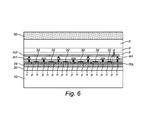
- Fig. 6 shows a cross-sectional view of the electronic device in accordance with another embodiment of the invention, having a series of two diodes as rectifying element.
- the main difference between Fig. 5 and 6 . Is that in Fig. 6 the dopants in the poly diode layer PDL are formed such that a NPNP region forming three PN-junctions in between two neighboring connections. However, the respective middle junctions are short circuited by means of respective silicide regions 32, which means that two PN-junctions are effectively connected in series.
- Fig. 7 shows the results of a TLP evaluation of the embodiment of Fig. 4 . Ruggedness can be evaluated using a TLP (Transmission Line Pulse) system. TLP tests and systems as such are well-known to the person skilled in the art. A TLP test is often used for ESD characterization, but can also be used for ruggedness evaluation.
- Fig. 7 shows two curves wherein the TLP current TLPC is plotted against the TLP voltage TLPV.
- the first curve Crv1 represents an RF-LDMOS transistor without a protection circuit 2
- the second curve Crv2 represents an RF-LDMOS transistor with a protection circuit as presented in Fig. 3 . It can be clearly observed from the curves that due to the protection circuit of the invention the current capability significantly increases.
- substrate may denote any suitable material, such as a semiconductor, glass, plastic, etc. According to an exemplary embodiment, the term “substrate” may be used to define generally the elements for layers that underlie and/or overlie a layer or a portion of interest. Also, the substrate may be any other base on which a layer is formed, for example a semiconductor wafer such as a silicon wafer or silicon chip.
- a semiconductor substrate may comprise a material of the group comprising: a group IV semiconductor (such as silicon or germanium), and a group III-group V compound semiconductor (such as gallium arsenide).
- semiconductor device may denote a transistor or a circuit comprising a plurality of transistors and interconnections.
- the transistor may be a field effect transistor for example.
- FET field effect transistor
- MOSFET complementary metal-oxide-semiconductor
- the semiconductor device can be any integrated circuit and may comprise logic circuitry, photo sensitive cells, memory cells, and the like.
- the material of the semiconductor structure may be silicon, germanium, or any other semiconductor material.
- any reference signs placed between parentheses shall not be construed as limiting the claim.
- Use of the verb "comprise” and its conjugations does not exclude the presence of elements or steps other than those stated in a claim.
- the article "a” or “an” preceding an element does not exclude the presence of a plurality of such elements.
- the invention may be implemented by means of hardware comprising several distinct elements, and by means of a suitably programmed computer. In the device claim enumerating several means, several of these means may be embodied by one and the same item of hardware. The mere fact that certain measures are recited in mutually different dependent claims does not indicate that a combination of these measures cannot be used to advantage.
Abstract
Description
- The invention relates to an electronic device comprising an RF-LDMOS transistor and a protection circuit for the RF-LDMOS transistor.
- In base stations for personal communication systems (GSM, EDGE, W-CDMA), RF-power amplifiers (PA) are key components. For these power amplifiers, RF Laterally Diffused MOS (LDMOS) transistors are the standard choice of technology, because of their excellent power capabilities gain, linearity and reliability.
- An RF power amplifier is a type of electronic amplifier used to convert a low-power radio-frequency signal into a larger signal of significant power, typically for driving the antenna of a transmitter. It is usually optimized to have high efficiency, high output Power (P1dB) compression, good return loss on the input and output, good gain, and optimum heat dissipation. The basic applications of the RF power amplifier include driving another high power source, driving a transmitting antenna, microwave heating, and exciting resonant cavity structures. Among these applications, driving transmitter antennas is most well-known. The transmitter-receivers are used not only for voice and data communication but also for weather sensing (in the form of radar).
- An RF power amplifier generally comprises of a package having a source lead (plate shaped), a drain lead, and a gate lead. Inside the package there is provided a semiconductor die in which the RF power transistor is manufactured. Depending on the size of the semiconductor die, there may also be a capacitor (MOSCAP) provided at the gate side of the die and there may be a further capacitor at the drain side. The capacitor(s) are added for impedance matching of the semiconductor die to the outside world. The die is wire bonded to the respective leads. For (electrical) performance reasons, the bond wires are kept as short as possible. Power amplifiers (PA's) for base stations use predominantly laterally-diffused metal-oxide-semiconductor (LDMOS) technology. The trend in base station PA's is towards higher peak power capabilities to be able to transmit more channels for larger data capacity. Modern LDMOS dies are designed in such a way that the gate and drain contacts are at the topside of the die and the source contact is on the backside of the die. The LDMOS packages are designed to fit this configuration. The gate and drain can be connected to the leads through bond wires. The source is connected to the bottom (lead) of the package (flange) using the backside contact of the die. The flange acts as a third lead. This configuration ensures a very short connection between the die and the third lead (source). This back-side contacting of the source is only possible in case the substrate of the die is conducting, which is the case in silicon-based LDMOS technology.
- Another important performance indicator for power RF-LDMOS transistors is the RF-ruggedness. This RF-ruggedness may be defined as the ability to withstand reflected power at the output. Power is reflected at the output if an impedance mismatch occurs. This may occurs as an incident (e.g. at breaking of the antenna) or as a structural, normal part of the application (e.g. at switching on a lamp). The amount of reflected power a device is able to withstand is expressed in the voltage standing wave ratio (VSWR) this device is able survive (without breaking down). In many LDMOS products for base stations, a VSWR of 1:10 is specified. In an RF power amplifier the reflected power causes voltage peaks at the drain of the LDMOS in the amplifier stage. If this voltage becomes too high, the device is destroyed.
- In the prior art several solutions to this problem have been proposed.
- A first solution concerns the protection of a power amplifier (PA) for VSWR-mismatch by using a circulator (http://en.wiki edia.org/wiki/Circulator) at the output of the device. This is a very expensive solution.
- Another solution is reported in
US4,122,400 . This published patent discloses a protection circuit for a transmitter amplifier, in which separate VSWR (reflected power) control and separate temperature control is provided when the thresholds of either or both are exceeded. When the temperature of the RF amplifier is sensed and when this temperature exceeds a certain threshold level, the output level of the RF amplifier is adjusted to protect the amplifier. Separately, there is provided a means for sensing the ration of the reflected power to the forward power (by an expensive directional couple) and when this ration exceeds a given threshold, the gain of the amplifier is cut back to thereby protect the amplifier. - A further solution is reported in
US6,794,719B2 in which an integrated diode is proposed for ruggedness improvement of a high-voltage (HV) LDMOS transistor. However, this solution is not suitable for RF-applications. In this solution the diode must cope with a high current and high voltage (breakdown voltage of the diode), which gives large power dissipation. To avoid thermal damage a large diode must be used, which gives a large capacitance, and this gives a decrease in RF-performance. - Further ruggedness can obtained increasing the intrinsic ruggedness of the LDMOS itself. This is done by avoiding the turn-on of the bipolar NPN-transistor, which is inherently present in an LDMOS transistor. If this parasitic bipolar transistor is switching on, the device is destroyed. Avoiding turning-on of the bipolar transistor can be done by electrical field engineering, and/or lowering the base resistance of the bipolar. This is also described in publication of S.J.C.H. Theeuwen et al. al., "LDMOS Ruggedness reliability", Microwave Journal, Vol. 52 / No. 4 / April 2009 / p. 96-104. However, there will always remain a trade-off between RF-performance versus intrinsic ruggedness. Furthermore, for future development of LDMOS on high resistivity substrate, it will become very hard to introduce sufficient intrinsic ruggedness into the power RF-LDMOS.
- One of the objects of the invention is to provide an electronic device comprising an RF-LDMOS transistor having an improved RF ruggedness, while not, or at least to a much lesser extent, compromising the RF performance of the RF-LDMOS transistor.
- The invention is defined by the independent claims, the dependent claims define embodiments.
- A first aspect of the invention provides an electronic device as claimed in
claim 1. The electronic device comprises an RF-LDMOS transistor and a protection circuit for the RF-LDMOS transistor. The protection circuit comprises: - an input terminal coupled to a drain terminal of the RF-LDMOS transistor;
- a clipping node;
- a clipping circuit coupled to the clipping node for substantially keeping the voltage on the clipping node below a predefined reference voltage, wherein the predefined reference voltage is designed to be larger than the operation voltage on the drain terminal and lower than a trigger voltage of a parasitic bipolar transistor that is inherently present in the RF-LDMOS transistor;
- a capacitance coupled between the clipping node and a further reference voltage terminal, and
- a rectifying element connected with its anode terminal to the input terminal and with its cathode terminal to the clipping node.
- An electronic device in accordance with the first aspect of the invention reaches several effects. First of all, the coupling of the drain terminal of the RF-LDMOS transistor to the clipping node (which is being kept below a predefined reference voltage (there are multiple ways of achieving this effect), wherein the predefined reference voltage is designed to be larger than the operation voltage on the drain terminal) via the rectifying element ensures that during normal RF operation, the voltage on the clipping node will approach (but most likely stay below) the predefined reference voltage, which means that the rectifying element is reverse biased. Thus, in normal operation, the impedance at the clipping node is not significantly loading the drain terminal of the RF-LDMOS transistor. Then, during a ruggedness event, the voltage on the drain terminal may get larger than the predefined reference voltage (which must be carefully chosen in order not to degrade the performance of the device when set too near to the operation voltage on the drain terminal). In this case the rectifying element may get forward biased and a (large) current will flow through the rectifying element (for example comprising one or more diodes) to the clipping node. This current may charge up the capacitance at the clipping node to a level higher than the predefined reference voltage. After the ruggedness event, the capacitance will de-charge to the predefined reference voltage. It is important to note that in the invention the rectifying element (for instance a diode or a series of diodes) only has to cope with large ruggedness currents in forward mode. This results in low power dissipation in the rectifying element, in particular when a diode or a series of diodes is used, because of the low voltage drop over the rectifying element (diode). A consequence of this, is that the rectifying element can be kept small in size, which is also beneficial for parasitic capacitances, which will consequently remain small as well. The latter being beneficial for the RF performance (due to a smaller degradation of RF behavior) of the electronic device.
- To facilitate the understanding of the scope of the invention and its variations, a few terms are defined hereinafter.
- Throughout this description the term "operation voltage" on a particular node should be considered as the voltage which that particular node has during normal operation of the device, which is typically the supply voltage added with the RF-voltage swing.
- Throughout this description the term "voltage" (of a particular node) should be considered as a potential difference between the respective potential (on that particular node) and a reference potential. In principle, such reference potential may be freely chosen, but for convenience in this description the source potential of the RF-LDMOS transistor is defined as the reference potential.
- Throughout this description the term "anode terminal" (of a rectifying element such as a diode) should be considered as the input terminal of the rectifying element. Furthermore, throughout this description the term "cathode terminal" should be considered as the output terminal of the rectifying element. Thus, the rectifying element is forward-biased when the anode terminal has a higher potential than the cathode terminal (and a large current may flow from anode to cathode), and the rectifying element is reverse-biased when the anode terminal has a lower potential than the cathode terminal (and a small leaking current may flow from anode to cathode).
- In an embodiment the clipping circuit comprises: i) a reference voltage terminal for being coupled to the predefined reference voltage, and ii) a connector coupled between the clipping node and the reference voltage terminal. This embodiment constitutes a first main variant of forming a clipping circuit that substantially keeps the voltage on the clipping node below a predefined reference voltage. In an embodiment the connector may be formed by a respective bondwire coupled between the clipping node and the reference voltage terminal.
- In an embodiment the clipping circuit comprises a further rectifying element connected with its cathode terminal to the clipping node and with its anode terminal to the further reference voltage terminal. This embodiment constitutes a second main variant of forming a clipping circuit that substantially keeps the voltage on the clipping node below a predefined reference voltage. In an embodiment the further rectifying element comprises a diode and the capacitance is formed by the parasitic capacitance of the diode.
- In an embodiment the further reference voltage is the voltage of the source terminal of RF-LDMOS transistor. Even though it is not very important to what reference voltage the capacitance is coupled, it still is advantageous to select the voltage (potential) on the source terminal as the further reference voltage, because this is the only reference plane which is available in a conventional RF-LDMOS transistor. Thus, this embodiment makes the generation and routing of the further reference voltage superfluous.
- In an embodiment the rectifying element comprises a single diode.
- In an embodiment the rectifying comprises a plurality of diodes connected in series. This embodiment is advantageous if the break-down voltage of a single diode is below the reference voltage. The break-down voltage of a single diode manufactured in a polysilicon wire may be typically in the range from 1V to 30V. However, it is expected that break-down voltages up to 70V are possible when the process and design are optimized.
- In an embodiment the further rectifying element comprises a single diode. In accordance with an aspect of the invention such diode must have a break-down voltage equal to the reference voltage.
- In an embodiment the further rectifying element comprises a plurality of diodes connected in series. This embodiment is useful if the break-down voltage of a single diode is lower than the reference voltage (for example half the reference voltage).
- In an embodiment the RF-LDMOS transistor and the protection circuit are integrated on a single substrate. In an advantageous embodiment this substrate is a silicon-on-insulator (SOI) substrate.
- In an embodiment the RF-LDMOS transistor comprises a drain bondpad in an upper interconnect layer forming the drain terminal, wherein at least part of the clipping circuit is substantially laid out underneath the drain bondpad. The bondpad may also be a bond bar (onto which a plurality of bond wires may be bonded. Preferably, in this embodiment the respective rectifying element is manufactured in a poly-silicon wire, wherein a junction has been formed by implanting n-type and p-type dopants in the respective wire. It is very convenient to implement the diodes in a poly silicon wire, as such diodes can easily be integrated underneath the drain bondpad, while having a relatively low parasitic capacitance to the substrate. In other words, the diodes could be implemented in the substrate, but this is then at the penalty of a higher capacitance to the substrate.
- A second aspect of the invention provides a power amplifier comprising the electronic device according to the invention. Such power amplifier benefits from the better ruggedness of the electronic device of the invention.
- A third aspect of the invention provides an integrated multi-stage power amplifier module comprising one or more electronic devices according to the invention. Such multi-stage power amplifier benefits from the better ruggedness of the electronic device of the invention.
- A fourth aspect of the invention provides a cellular base station comprising the electronic device. Such cellular base station benefits from the better ruggedness of the electronic device of the invention.
- These and other aspects of the invention are apparent from and will be elucidated with reference to the embodiments described hereinafter. In the drawings,
-
Fig. 1 shows a schematic cross-sectional view of an RF-LDMOS transistor as known from the prior art; -
Fig. 2 shows an equivalent circuit diagram of an electronic device in accordance with a first embodiment of the invention; -
Fig. 3 shows an equivalent circuit diagram of an electronic device in accordance with a second embodiment of the invention; -
Fig. 4 shows a layout of the electronic device ofFig. 3 ; -
Fig. 5 shows a cross-sectional view of the electronic device in accordance with another embodiment of the invention, having a single diode as rectifying element; -
Fig. 6 shows a cross-sectional view of the electronic device in accordance with another embodiment of the invention, having a series of two diodes as rectifying element, and; -
Fig. 7 shows the results of a TLP evaluation of the embodiment ofFig. 4 . -
- 1
- RF-LDMOS transistor
- 10
- substrate
- 20
- P-type EPI-layer
- 21
- P-type sinker layer (connecting source region to substrate/source terminal)
- 22
- P-type well region (comprising channel region of RF-LDMOS transistor)
- 23
- N-type drain extension layer of LDMOS transistor
- 24
- N-type source region
- 25
- N-type drain region
- 26
- Silicide layer (connecting P-
type sinker layer 21 to N-type source region) - 27
- gate dielectric (dielectric layer)
- 28
- further dielectric layer (isolating
shield 35 from gate 30) - 30
- gate
- 35
- shield
- 40
- source line
- 45
- connecting stack for drain line
- 50
- drain line
- 100
- parasitic bipolar transistor
- 2
- protection circuit
- 3
- clipping circuit
- Vdd
- supply voltage
- Gnd
- ground voltage
- Ni
- input terminal of protection circuit
- Nc
- clipping node
- Drn
- drain terminal of LDMOS transistor
- Src
- source terminal of LDMOS transistor
- Gte
- gate terminal of LDMOS transistor
- Ld
- drain terminal bondwire (inductance)
- Lr
- reference terminal bondwire
- Vref
- reference voltage
- D1, D2
- rectifying elements (diodes)
- Ct
- capacitance
- 3'
- alternative clipping circuit
- Dcl
- clipping diode
- Gbb
- gate bondbar (gate bondpad)
- Dbb
- drain bondbar (drain bondpad)
- 29
- field oxide (LOCOS)
- 32
- silicide regions (connecting poly diodes in series)
- 60
- scratch protection layer (Si3N4-layer)
- M1
- first metal layer
- M2
- second metal layer
- PDL
- poly diode layer
- d
- dielectric layers
- p
- p-type doped region
- n
- n-type doped region
- Crv1
- first curve (without protection circuit)
- Crv2
- second curve (with protection circuit)
- TLPC
- TLP current
- TLPV
- TLP voltage
- In this description an RF-LDMOS transistor with an ruggedness protection is proposed. In specific embodiments this protection is integrated on the same substrate. With the use of ruggedness protection circuit the voltage spikes, which occur if power is reflected, can be clipped. This provides protection for the RF-LDMOS. The protection is preferably integrated directly on the drain of the RF-LDMOS. If the protection is provided as an external component, the phase difference between the actual drain of the LDMOS and the ruggedness protection circuit may make the protection less effective. Integrating the protection on the LDMOS die therefore improves the RF performance.
- The advantages of the ruggedness protection of the invention are:
- The parasitic capacitance of the ruggedness protection is small. A large capacitance results in large losses in the capacitance, which will decrease the efficiency of the LDMOS transistor; and
- The ruggedness protection has a high current capability. During a ruggedness event a high current may flow to prevent the voltage to increase further. These aspect will be elucidated in the description of the embodiments hereinafter.
- To facilitate the understanding of the scope of the invention and its variations, a few terms are defined hereinafter.
- Throughout this description the term "interconnect layer" should be considered as synonym to "metallization layer" or "metal layer". Both terms are used interchangeably and have to be interpreted as the layer comprising conductors, the insulating layer in which the conductors are embedded, and any vias (=contacts) to underlying layers. These terms are well-known to the person skilled in the art of semiconductor technology.
- In this description the term "RF power amplifier" refers to a circuit used to convert a low-power radio-frequency signal into a larger signal of significant power, typically for driving the antenna of a transmitter
-
Fig. 1 shows a schematic cross-sectional view of an RF-LDMOS transistor as known from the prior art. The RF-LDMOS transistor 1 is integrated on a P-type substrate 10. On thesubstrate 10 there is provided an P-type epitaxial (EPI)layer 20. In the P-type epitaxial layer 20 an P-type sinker layer 21 is formed for establishing an electrical contact with the P-type substrate 10 of which the back-side forms the source contact of the RF-LDMOS transistor. Adjacent the P-type sinker layer 21 there is provided a P-well region 22, which comprises the channel region of the RF-LDMOS transistor. The EP-layer 20 further comprises an N-type drain extension layer 23 (weakly doped for forming a high resistance), a heavily-doped N-type source region 24, and a heavily-doped N-type drain region 25, wherein thedrain extension layer 23 is situated in between the channel region and thedrain region 25. Asilicide layer 26 is provided on the P-type sinker layer 21 and on part of the N-type source region 24. Thissilicide layer 26 effectively connects thesource region 24 to thesubstrate 10. On top of thesilicide layer 26 there is provided asource line 40 for connecting a plurality of source regions (not shown) together. Above thedrain region 25 there is provided adrain line 50 and a connectingstack 45 for connecting thedrain line 50 to thedrain region 25. On the channel region there is further provided a dielectric layer/gate dielectric 27 (for example comprising silicon oxide) extending form an end of thesilicide layer 26 to the connectingstack 45 for thedrain line 50. On top of thegate dielectric 27 there is provided agate 30 being capacitively coupled to the channel region in between thesource region 24 and thedrain extension layer 23. Over thegate 30 and thegate dielectric layer 27 there is provided afurther dielectric layer 28. On top of thefurther dielectric layer 28 there is provided ashield 35. Theshield 35 serves as an electrical shield between thedrain line 50 and thegate 30. It must be noted thatFig. 1 discloses an N-type RF-LDMOS transistor 1. A P-type RF-LDMOS transistor is obtained if the respective conductivity types of thesource region 23, channel region,drain extension region 23, and drainregion 25 are reversed. However, such P-type RF-LDMOS transistor has a lower performance (when the size is kept constant), due to the lower mobility of the majority carriers (holes) in the channel region. - In the RF-LDMOS transistor of
Fig. 1 there is inherently present an NPN parasiticbipolar transistor 100, indicated by the rectangle. It is important to note that this NPN parasiticbipolar transistor 100 has a low gain. Nevertheless, it may happen that this bipolar transistor is switched 100 during operation, in particular in case of reflections at the output of the RF-LDMOS transistor due to impedance mismatch. During such reflections the voltage on the drain may get too high, switching on thebipolar transistor 100, which then directly destroys thedevice 1. -
Fig. 2 shows an equivalent circuit diagram of an electronic device in accordance with a first embodiment of the invention. On the left side ofFig. 2 there is shown the RF-LDMOS transistor 1 which is connected, via a drain terminal bondwire Ld (with an inductance), with its drain terminal Drn to a drain lead connected to a power supply voltage Vdd. This supply voltage Vdd is typically within the range of 28V to 50V. An LDMOS device optimized for 28V will have slightly other dimensions then the 50V variant. The RF-LDMOS transistor also comprises a gate terminal Gte which is typically connected to a gate lead via a further bondwire (not shown). The source terminal Src of theLDMOS transistor 1 is connected to the ground voltage (potential) Gnd. As already mentioned the source terminal of the RF-LDMOS is typically at the backside of a substrate. Typically, the substrate onto which the RF-LDMOS is manufactured is directly provided on and in electrical contact with a source lead. - The electronic device further comprises a
protection circuit 2. Theprotection circuit 2 comprises aclipping circuit 3. Theprotection circuit 2 has an input terminal Ni which is coupled to the drain terminal Drn of theLDMOS transistor 1. The input terminal Ni is connected to a series connected of two diodes D1, D2, which together form an implementation of a rectifying element. The rectifying element is connected such that its anode side is coupled to the drain terminal Drn. The cathode side of the rectifying element is coupled to a clipping node Nc. The clipping node Nc forms part of theclipping circuit 3. The clipping circuit comprises a reference terminal bondwire Lr (with an inductance) coupled between the clipping node Nc and a reference voltage terminal being at a reference voltage Vref. Theclipping circuit 3 further comprises a capacitance Ct coupled between the clipping node Nc and a further reference voltage terminal being at ground voltage Gnd. - As is shown in
Fig. 2 , the diodes D1, D2 are provided directly on the drain terminal Drn of theLDMOS transistor 1. For this purpose, a poly diode is advantageous. These diodes can be integrated on top of the locos oxide, which results in a low capacitance to ground. The breakdown voltage of the diode should be above the reference voltage which is Vref applied via the reference terminal bondwire Lr. If the diode has a breakdown voltage below this reference voltage, a series of diodes can be used as illustrated inFig. 2 . - In this embodiment the diode(s) D1, D2 are connected to an integrated grounded capacitance Ct, which is also connected to an external lead to supply the reference voltage Vref.
- The value of the reference voltage Vref should be so low as possible, so the
protection circuit 2 switches on as early as possible in case of a ruggedness event. However, if the reference voltage Vref is set too low, the RF-performance will degrade. So, it is advantageous to use a value larger than two times the supply voltage Vdd. During normal RF operation, the voltage across capacitance Ct will be substantially equal to the reference voltage Vref. The voltage at the drain terminal Drn of the RF-LDMOS transistor will be below this level. The poly diodes D1, D2 will be in reverse, and no significant current will flow through them. - During a ruggedness event, the voltage direct on the drain terminal, can get higher than the reference voltage Vref. Now, the diodes D1, D2 are forward biased and a (large) current flows through the diodes D1, D2. This current may charge up the capacitance Ct. After the ruggedness event, the capacitance Ct will discharge to the reference voltage Vref, while delivering power to the voltage source which is used to generate Vref.
- A key aspect of the invention is that the (poly) diodes only have to cope with the large ruggedness current in forward-bias mode. This gives a relative low dissipation in to diodes D1, D2, because of the low voltage drop across the diodes. Consequence is that the (poly) diodes can be relative small. This relative small size of the diodes is giving a small capacitance of the diode and so only a small degradation of RF-behavior.
-
Fig. 3 shows an equivalent circuit diagram of an electronic device in accordance with a second embodiment of the invention. This embodiment will be discussed in as far as it differs fromFig. 2 . Sometimes, it may be inconvenient to feed the extra reference voltage Vref via additional bondwires to the chip. In the embodiment ofFig. 3 the reference voltage is created on the die itself. The main difference betweenFig. 3 and Fig. 2 is that inFig. 3 there is an alternative clipping circuit 3'. The alternative clipping circuit 3' comprises the capacitance Ct and a clipping diode Dcl connected in parallel with the capacitance Ct, wherein the anode side of the clipping diode Dcl is connected to the ground voltage (further reference voltage terminal), i.e. in normal operation the clipping diode Dcl is reverse-biased. - A clipping diode Dcl with a breakdown voltage equal to the earlier mentioned reference voltage Vref in
Fig. 2 , is integrated near to capacitance Ct. This clipping diode Dcl must be able to dissipate the high power associated with a ruggedness event. Therefore, the thermal resistance of the diode should be low and, preferably, a diode that is integrated in the (silicon) substrate should be used. Furthermore, the diode Dcl must be relative large. - The large clipping diode Dcl has a large capacitance to ground, however since the capacitance of the (poly) diodes D1, D2 is low, and this doesn't load the drain of the RF-LDMOS. It must be noted that even though a separate capacitance Ct has been drawn in
Fig. 3 , this capacitance may also be (at least) partially formed by the parasitic capacitance of the clipping diode Dcl. - At switch-on of the circuit, the RF-signal at the drain Drn will charge up the capacitance Ct. After this charging up, the behavior of this embodiment is the same as for embodiment of
Fig. 2 . However, in this case the energy associated with the ruggedness event cannot be delivered back to the power supply. Instead of that, the energy is dissipated in the clipping diode Dcl. -
Fig. 4 shows a layout of the electronic device ofFig. 3 . This figure merely serves to illustrate the feasibility of the invention. By no means, the invention is limited to this specific layout. There are literally thousands of layout implementations possible. In the layout inFig. 4 there is visible a gate bondbar Gbb (a bondbar is a bondpad suitable for bonding a plurality of bond wires) and a drain bondbar Dbb, wherein between theLDMOS transistor 1 is laid out (including its drain and gate fingers). In this embodiment the rectifying element (in the form of a series connection of two diodes D1, D2) is laid out at least partially underneath the drain bondbar Dbb, which saves space. The clipping diode Dcl is also laid out underneath the drain bondbar Dbb, but then in the substrate (a junction formed by a diffusion in the substrate). -
Fig. 5 shows a cross-sectional view of the electronic device in accordance with another embodiment of the invention, having a single diode as rectifying element. Reference is also made to the description ofFig. 1 , including the reference numbers used in that figure. InFig. 5 there is shown thesubstrate 10 provided with the N-type EPI-layer 20 on top of it. On the EPI-layer 20 there is provided a field oxide layer 29 (this may be a LOCOS layer, but alternatively, this could be an shallow-trench-isolation (STI) layer. On top of thefield oxide layer 29 there is provided the poly diode layer PDL which comprises P-type doped regions p and N-type doped regions n, alternatingly. All P-type doped regions p are connected together via a first metal layer M1 (connected to the diodes via respective contacts). All N-type doped regions n are connected together via a second metal layer M2 (connected to the diodes via respective vias, first metal layer parts, and contacts). In between the respective poly diode layer PDL and the metal layers M1, M2 there is provided respective dielectric layers d. On top of the layer stack there is provided a scratch protection layer 60 (typically comprising silicon nitride (Si3N4)). -
Fig. 6 shows a cross-sectional view of the electronic device in accordance with another embodiment of the invention, having a series of two diodes as rectifying element. The main difference betweenFig. 5 and6 . Is that inFig. 6 the dopants in the poly diode layer PDL are formed such that a NPNP region forming three PN-junctions in between two neighboring connections. However, the respective middle junctions are short circuited by means ofrespective silicide regions 32, which means that two PN-junctions are effectively connected in series. -
Fig. 7 shows the results of a TLP evaluation of the embodiment ofFig. 4 .
Ruggedness can be evaluated using a TLP (Transmission Line Pulse) system. TLP tests and systems as such are well-known to the person skilled in the art. A TLP test is often used for ESD characterization, but can also be used for ruggedness evaluation.Fig. 7 shows two curves wherein the TLP current TLPC is plotted against the TLP voltage TLPV. The first curve Crv1 represents an RF-LDMOS transistor without aprotection circuit 2, and the second curve Crv2 represents an RF-LDMOS transistor with a protection circuit as presented inFig. 3 . It can be clearly observed from the curves that due to the protection circuit of the invention the current capability significantly increases. - The term "substrate" may denote any suitable material, such as a semiconductor, glass, plastic, etc. According to an exemplary embodiment, the term "substrate" may be used to define generally the elements for layers that underlie and/or overlie a layer or a portion of interest. Also, the substrate may be any other base on which a layer is formed, for example a semiconductor wafer such as a silicon wafer or silicon chip. A semiconductor substrate may comprise a material of the group comprising: a group IV semiconductor (such as silicon or germanium), and a group III-group V compound semiconductor (such as gallium arsenide).
- The term "semiconductor device" may denote a transistor or a circuit comprising a plurality of transistors and interconnections. The transistor may be a field effect transistor for example.
- The term "field effect transistor" (FET) may denote a transistor in which an output current (source-drain current) may be controlled by the voltage applied to a gate. Such FET structure may be an MOSFET. The semiconductor device can be any integrated circuit and may comprise logic circuitry, photo sensitive cells, memory cells, and the like. The material of the semiconductor structure may be silicon, germanium, or any other semiconductor material.
- As the invention is related towards technology rather than circuits the following description of the drawings does not elaborate in much detail on the operation of CCD and CMOS imagers. Such knowledge is considered to be known to the person skilled in the art.
- It should be noted that the above-mentioned embodiments illustrate rather than limit the invention, and that those skilled in the art will be able to design many alternative embodiments.
- In the claims, any reference signs placed between parentheses shall not be construed as limiting the claim. Use of the verb "comprise" and its conjugations does not exclude the presence of elements or steps other than those stated in a claim. The article "a" or "an" preceding an element does not exclude the presence of a plurality of such elements. The invention may be implemented by means of hardware comprising several distinct elements, and by means of a suitably programmed computer. In the device claim enumerating several means, several of these means may be embodied by one and the same item of hardware. The mere fact that certain measures are recited in mutually different dependent claims does not indicate that a combination of these measures cannot be used to advantage.
Claims (15)
- An electronic device comprising an RF-LDMOS transistor (1) and a protection circuit (2) for the RF-LDMOS transistor, the protection circuit (2) comprising:- an input terminal (Ni) coupled to a drain terminal (Drn) of the RF-LDMOS transistor (1);- a clipping node (Nc);- a clipping circuit (3) coupled to the clipping node (Nc) for substantially keeping the voltage on the clipping node (Nc) below a predefined reference voltage, wherein the predefined reference voltage is designed to be larger than the operation voltage on the drain terminal (Drn) and lower than a trigger voltage of a parasitic bipolar transistor (100) that is inherently present in the RF-LDMOS transistor;- a capacitance (Ct) coupled between the clipping node (Nc) and a further reference voltage terminal (Gnd), and- a rectifying element (D1, D2) connected with its anode terminal to the input terminal (Ni) and with its cathode terminal to the clipping node (Nc).
- The electronic device as claimed in claim 1, wherein the clipping circuit (3) comprises: i) a reference voltage terminal for being coupled to the predefined reference voltage (Vref), and ii) a connector (Lr) coupled between the clipping node (Nc) and the reference voltage terminal.
- The electronic device as claimed in claim 2, wherein the connector (Lr) is formed by a respective bondwire coupled between the clipping node (Nc) and the reference voltage terminal.
- The electronic device as claimed in claim 1, wherein the clipping circuit (3) comprises a further rectifying element (Dcl) connected with its cathode terminal to the clipping node (Nc) and with its anode terminal to the further reference voltage terminal (Gnd).
- The electronic device as claimed in claim 4, wherein the further rectifying element (Dcl) comprises a diode and the capacitance (Ct) is formed by the parasitic capacitance of the diode (Dcl).
- The electronic device as claimed in any one of claims 2 to 5, wherein the further reference voltage (Gnd) is the voltage of the source terminal (Src) of RF-LDMOS transistor (1).
- The electronic device as claimed in any one of the preceding claims, wherein the rectifying element comprises a single diode (D1).
- The electronic device as claimed in any one of claims 1 to 6, wherein the rectifying element comprises a plurality of diodes connected in series (D1, D2).
- The electronic device as claimed in any one of the preceding claims, wherein the further rectifying element comprises a single diode (Dcl).
- The electronic device as claimed in any one of claims 1 to 8, wherein the further rectifying element comprises a plurality of diodes connected in series.
- The electronic device as claimed in any one of the preceding claims, wherein the RF-LDMOS transistor (1) and the protection circuit (2) are integrated on a single substrate (10).
- The electronic device as claimed in claim 11, wherein the RF-LDMOS transistor (1) comprises a drain bondpad (Dbb) in an upper interconnect layer forming the drain terminal (Drn), wherein at least part of the clipping circuit (3) is substantially laid out underneath the drain bondpad (Dbb).
- A power amplifier comprising the electronic device according to any one of claims 1-12.
- An integrated multi-stage power amplifier module comprising one or more electronic devices according to any of claims 1-12.
- A cellular base station comprising the electronic device according to any of claims 1-12.
Priority Applications (3)
| Application Number | Priority Date | Filing Date | Title |
|---|---|---|---|
| EP12167901.3A EP2665187B1 (en) | 2012-05-14 | 2012-05-14 | Electronic device comprising RF-LDMOS transistor having improved ruggedness |
| US13/887,212 US9019671B2 (en) | 2012-05-14 | 2013-05-03 | Electronic device comprising RF-LDMOS transistor having improved ruggedness |
| CN201310176747.8A CN103475320B (en) | 2012-05-14 | 2013-05-14 | Electronic device comprising RF-LDMOS transistor having improved ruggedness |
Applications Claiming Priority (1)
| Application Number | Priority Date | Filing Date | Title |
|---|---|---|---|
| EP12167901.3A EP2665187B1 (en) | 2012-05-14 | 2012-05-14 | Electronic device comprising RF-LDMOS transistor having improved ruggedness |
Publications (2)
| Publication Number | Publication Date |
|---|---|
| EP2665187A1 true EP2665187A1 (en) | 2013-11-20 |
| EP2665187B1 EP2665187B1 (en) | 2016-07-20 |
Family
ID=46052660
Family Applications (1)
| Application Number | Title | Priority Date | Filing Date |
|---|---|---|---|
| EP12167901.3A Not-in-force EP2665187B1 (en) | 2012-05-14 | 2012-05-14 | Electronic device comprising RF-LDMOS transistor having improved ruggedness |
Country Status (3)
| Country | Link |
|---|---|
| US (1) | US9019671B2 (en) |
| EP (1) | EP2665187B1 (en) |
| CN (1) | CN103475320B (en) |
Families Citing this family (4)
| Publication number | Priority date | Publication date | Assignee | Title |
|---|---|---|---|---|
| DE102013226511B4 (en) | 2013-12-18 | 2016-12-15 | TRUMPF Hüttinger GmbH + Co. KG | Power supply system and method for generating a power |
| DE102013226537B4 (en) | 2013-12-18 | 2022-12-29 | TRUMPF Hüttinger GmbH + Co. KG | Power supply system with multiple amplifier paths and method for exciting a plasma |
| JP6318911B2 (en) * | 2014-06-26 | 2018-05-09 | 株式会社デンソー | Semiconductor device inspection circuit and inspection method |
| CN108540099A (en) * | 2017-03-06 | 2018-09-14 | 上海安其威微电子科技有限公司 | SOI amplifiers |
Citations (6)
| Publication number | Priority date | Publication date | Assignee | Title |
|---|---|---|---|---|
| US4122400A (en) | 1976-11-08 | 1978-10-24 | Rca Corporation | Amplifier protection circuit |
| US6794719B2 (en) | 2001-06-28 | 2004-09-21 | Koninklijke Philips Electronics N.V. | HV-SOI LDMOS device with integrated diode to improve reliability and avalanche ruggedness |
| DE102005055832A1 (en) * | 2005-11-23 | 2007-05-24 | Patent-Treuhand-Gesellschaft für elektrische Glühlampen mbH | Circuit arrangement for controlling electronic component, has bipolar transistor provided in grounded-base circuit and having emitter coupled with output of microprocessor, and another bipolar transistor provided in grounded-emitter circuit |
| US20070249304A1 (en) * | 2005-03-25 | 2007-10-25 | Pulsewave Rf, Inc. | Radio frequency power amplifier and method using a controlled supply |
| US7787227B1 (en) * | 2008-04-24 | 2010-08-31 | Atheros Communications, Inc. | Apparatus and method for electrostatic discharge protection of a transmit integrated circuit |
| US20110309872A1 (en) * | 2010-06-17 | 2011-12-22 | Cynthia Blair | Voltage Spike Protection for Power DMOS Devices |
Family Cites Families (2)
| Publication number | Priority date | Publication date | Assignee | Title |
|---|---|---|---|---|
| EP2143205A1 (en) * | 2007-04-23 | 2010-01-13 | Freescale Semiconductor, Inc. | Circuit, integrated circuit and method for dissipating heat from an inductive load |
| KR101767577B1 (en) * | 2012-02-09 | 2017-08-23 | 스카이워크스 솔루션즈, 인코포레이티드 | Apparatus and methods for envelope tracking |
-
2012
- 2012-05-14 EP EP12167901.3A patent/EP2665187B1/en not_active Not-in-force
-
2013
- 2013-05-03 US US13/887,212 patent/US9019671B2/en not_active Expired - Fee Related
- 2013-05-14 CN CN201310176747.8A patent/CN103475320B/en not_active Expired - Fee Related
Patent Citations (6)
| Publication number | Priority date | Publication date | Assignee | Title |
|---|---|---|---|---|
| US4122400A (en) | 1976-11-08 | 1978-10-24 | Rca Corporation | Amplifier protection circuit |
| US6794719B2 (en) | 2001-06-28 | 2004-09-21 | Koninklijke Philips Electronics N.V. | HV-SOI LDMOS device with integrated diode to improve reliability and avalanche ruggedness |
| US20070249304A1 (en) * | 2005-03-25 | 2007-10-25 | Pulsewave Rf, Inc. | Radio frequency power amplifier and method using a controlled supply |
| DE102005055832A1 (en) * | 2005-11-23 | 2007-05-24 | Patent-Treuhand-Gesellschaft für elektrische Glühlampen mbH | Circuit arrangement for controlling electronic component, has bipolar transistor provided in grounded-base circuit and having emitter coupled with output of microprocessor, and another bipolar transistor provided in grounded-emitter circuit |
| US7787227B1 (en) * | 2008-04-24 | 2010-08-31 | Atheros Communications, Inc. | Apparatus and method for electrostatic discharge protection of a transmit integrated circuit |
| US20110309872A1 (en) * | 2010-06-17 | 2011-12-22 | Cynthia Blair | Voltage Spike Protection for Power DMOS Devices |
Non-Patent Citations (1)
| Title |
|---|
| S.J.C.H. THEEUWEN ET AL.: "LDMOS Ruggedness reliability", MICROWAVE JOURNAL, vol. 52, no. 4, April 2009 (2009-04-01), pages 96 - 104 |
Also Published As
| Publication number | Publication date |
|---|---|
| US20130307055A1 (en) | 2013-11-21 |
| CN103475320A (en) | 2013-12-25 |
| US9019671B2 (en) | 2015-04-28 |
| CN103475320B (en) | 2017-05-17 |
| EP2665187B1 (en) | 2016-07-20 |
Similar Documents
| Publication | Publication Date | Title |
|---|---|---|
| US9530773B2 (en) | Systems and methods for integrating bootstrap circuit elements in power transistors and other devices | |
| US6649944B2 (en) | Silicon-on-insulator diodes and ESD protection circuits | |
| TWI443836B (en) | Power device integration on a common substrate | |
| US6624487B1 (en) | Drain-extended MOS ESD protection structure | |
| US10446687B2 (en) | Integrated circuit connection arrangement for minimizing crosstalk | |
| US8471337B2 (en) | Integrated circuit | |
| US11276680B2 (en) | Power semiconductor device with integrated temperature protection | |
| US11335627B2 (en) | Connection arrangements for integrated lateral diffusion field effect transistors having a backside contact | |
| KR20080106951A (en) | Esd protection circuit with isolated diode element and method thereof | |
| TW201415609A (en) | Power device integration on a common substrate | |
| US11855012B2 (en) | Devices and methods for enhancing insertion loss performance of an antenna switch | |
| US9019671B2 (en) | Electronic device comprising RF-LDMOS transistor having improved ruggedness | |
| US6898060B2 (en) | Gated diode overvoltage protection | |
| US20230054117A1 (en) | Electro-static discharge protection device for semiconductor | |
| EP4229682A1 (en) | Integrated freewheeling diode and extraction device | |
| CN117616572A (en) | Semiconductor device and method for manufacturing the same |
Legal Events
| Date | Code | Title | Description |
|---|---|---|---|
| PUAI | Public reference made under article 153(3) epc to a published international application that has entered the european phase |
Free format text: ORIGINAL CODE: 0009012 |
|
| AK | Designated contracting states |
Kind code of ref document: A1 Designated state(s): AL AT BE BG CH CY CZ DE DK EE ES FI FR GB GR HR HU IE IS IT LI LT LU LV MC MK MT NL NO PL PT RO RS SE SI SK SM TR |
|
| AX | Request for extension of the european patent |
Extension state: BA ME |
|
| 17P | Request for examination filed |
Effective date: 20131031 |
|
| RBV | Designated contracting states (corrected) |
Designated state(s): AL AT BE BG CH CY CZ DE DK EE ES FI FR GB GR HR HU IE IS IT LI LT LU LV MC MK MT NL NO PL PT RO RS SE SI SK SM TR |
|
| 17Q | First examination report despatched |
Effective date: 20141028 |
|
| RAP1 | Party data changed (applicant data changed or rights of an application transferred) |
Owner name: SAMBA HOLDCO NETHERLANDS B.V. |
|
| GRAP | Despatch of communication of intention to grant a patent |
Free format text: ORIGINAL CODE: EPIDOSNIGR1 |
|
| GRAS | Grant fee paid |
Free format text: ORIGINAL CODE: EPIDOSNIGR3 |
|
| INTG | Intention to grant announced |
Effective date: 20160308 |
|
| RAP1 | Party data changed (applicant data changed or rights of an application transferred) |
Owner name: AMPLEON NETHERLANDS B.V. |
|
| GRAA | (expected) grant |
Free format text: ORIGINAL CODE: 0009210 |
|
| AK | Designated contracting states |
Kind code of ref document: B1 Designated state(s): AL AT BE BG CH CY CZ DE DK EE ES FI FR GB GR HR HU IE IS IT LI LT LU LV MC MK MT NL NO PL PT RO RS SE SI SK SM TR |
|
| REG | Reference to a national code |
Ref country code: GB Ref legal event code: FG4D |
|
| REG | Reference to a national code |
Ref country code: CH Ref legal event code: EP |
|
| REG | Reference to a national code |
Ref country code: IE Ref legal event code: FG4D |
|
| REG | Reference to a national code |
Ref country code: AT Ref legal event code: REF Ref document number: 814802 Country of ref document: AT Kind code of ref document: T Effective date: 20160815 |
|
| REG | Reference to a national code |
Ref country code: DE Ref legal event code: R096 Ref document number: 602012020621 Country of ref document: DE |
|
| REG | Reference to a national code |
Ref country code: NL Ref legal event code: FP |
|
| REG | Reference to a national code |
Ref country code: LT Ref legal event code: MG4D |
|
| REG | Reference to a national code |
Ref country code: AT Ref legal event code: MK05 Ref document number: 814802 Country of ref document: AT Kind code of ref document: T Effective date: 20160720 |
|
| PG25 | Lapsed in a contracting state [announced via postgrant information from national office to epo] |
Ref country code: IS Free format text: LAPSE BECAUSE OF FAILURE TO SUBMIT A TRANSLATION OF THE DESCRIPTION OR TO PAY THE FEE WITHIN THE PRESCRIBED TIME-LIMIT Effective date: 20161120 Ref country code: RS Free format text: LAPSE BECAUSE OF FAILURE TO SUBMIT A TRANSLATION OF THE DESCRIPTION OR TO PAY THE FEE WITHIN THE PRESCRIBED TIME-LIMIT Effective date: 20160720 Ref country code: NO Free format text: LAPSE BECAUSE OF FAILURE TO SUBMIT A TRANSLATION OF THE DESCRIPTION OR TO PAY THE FEE WITHIN THE PRESCRIBED TIME-LIMIT Effective date: 20161020 Ref country code: HR Free format text: LAPSE BECAUSE OF FAILURE TO SUBMIT A TRANSLATION OF THE DESCRIPTION OR TO PAY THE FEE WITHIN THE PRESCRIBED TIME-LIMIT Effective date: 20160720 Ref country code: LT Free format text: LAPSE BECAUSE OF FAILURE TO SUBMIT A TRANSLATION OF THE DESCRIPTION OR TO PAY THE FEE WITHIN THE PRESCRIBED TIME-LIMIT Effective date: 20160720 Ref country code: FI Free format text: LAPSE BECAUSE OF FAILURE TO SUBMIT A TRANSLATION OF THE DESCRIPTION OR TO PAY THE FEE WITHIN THE PRESCRIBED TIME-LIMIT Effective date: 20160720 Ref country code: IT Free format text: LAPSE BECAUSE OF FAILURE TO SUBMIT A TRANSLATION OF THE DESCRIPTION OR TO PAY THE FEE WITHIN THE PRESCRIBED TIME-LIMIT Effective date: 20160720 |
|
| PG25 | Lapsed in a contracting state [announced via postgrant information from national office to epo] |
Ref country code: PT Free format text: LAPSE BECAUSE OF FAILURE TO SUBMIT A TRANSLATION OF THE DESCRIPTION OR TO PAY THE FEE WITHIN THE PRESCRIBED TIME-LIMIT Effective date: 20161121 Ref country code: AT Free format text: LAPSE BECAUSE OF FAILURE TO SUBMIT A TRANSLATION OF THE DESCRIPTION OR TO PAY THE FEE WITHIN THE PRESCRIBED TIME-LIMIT Effective date: 20160720 Ref country code: SE Free format text: LAPSE BECAUSE OF FAILURE TO SUBMIT A TRANSLATION OF THE DESCRIPTION OR TO PAY THE FEE WITHIN THE PRESCRIBED TIME-LIMIT Effective date: 20160720 Ref country code: PL Free format text: LAPSE BECAUSE OF FAILURE TO SUBMIT A TRANSLATION OF THE DESCRIPTION OR TO PAY THE FEE WITHIN THE PRESCRIBED TIME-LIMIT Effective date: 20160720 Ref country code: ES Free format text: LAPSE BECAUSE OF FAILURE TO SUBMIT A TRANSLATION OF THE DESCRIPTION OR TO PAY THE FEE WITHIN THE PRESCRIBED TIME-LIMIT Effective date: 20160720 Ref country code: BE Free format text: LAPSE BECAUSE OF FAILURE TO SUBMIT A TRANSLATION OF THE DESCRIPTION OR TO PAY THE FEE WITHIN THE PRESCRIBED TIME-LIMIT Effective date: 20160720 Ref country code: GR Free format text: LAPSE BECAUSE OF FAILURE TO SUBMIT A TRANSLATION OF THE DESCRIPTION OR TO PAY THE FEE WITHIN THE PRESCRIBED TIME-LIMIT Effective date: 20161021 Ref country code: LV Free format text: LAPSE BECAUSE OF FAILURE TO SUBMIT A TRANSLATION OF THE DESCRIPTION OR TO PAY THE FEE WITHIN THE PRESCRIBED TIME-LIMIT Effective date: 20160720 |
|
| REG | Reference to a national code |
Ref country code: DE Ref legal event code: R097 Ref document number: 602012020621 Country of ref document: DE |
|
| PG25 | Lapsed in a contracting state [announced via postgrant information from national office to epo] |
Ref country code: RO Free format text: LAPSE BECAUSE OF FAILURE TO SUBMIT A TRANSLATION OF THE DESCRIPTION OR TO PAY THE FEE WITHIN THE PRESCRIBED TIME-LIMIT Effective date: 20160720 Ref country code: EE Free format text: LAPSE BECAUSE OF FAILURE TO SUBMIT A TRANSLATION OF THE DESCRIPTION OR TO PAY THE FEE WITHIN THE PRESCRIBED TIME-LIMIT Effective date: 20160720 |
|
| PLBE | No opposition filed within time limit |
Free format text: ORIGINAL CODE: 0009261 |
|
| STAA | Information on the status of an ep patent application or granted ep patent |
Free format text: STATUS: NO OPPOSITION FILED WITHIN TIME LIMIT |
|
| PG25 | Lapsed in a contracting state [announced via postgrant information from national office to epo] |
Ref country code: DK Free format text: LAPSE BECAUSE OF FAILURE TO SUBMIT A TRANSLATION OF THE DESCRIPTION OR TO PAY THE FEE WITHIN THE PRESCRIBED TIME-LIMIT Effective date: 20160720 Ref country code: CZ Free format text: LAPSE BECAUSE OF FAILURE TO SUBMIT A TRANSLATION OF THE DESCRIPTION OR TO PAY THE FEE WITHIN THE PRESCRIBED TIME-LIMIT Effective date: 20160720 Ref country code: SM Free format text: LAPSE BECAUSE OF FAILURE TO SUBMIT A TRANSLATION OF THE DESCRIPTION OR TO PAY THE FEE WITHIN THE PRESCRIBED TIME-LIMIT Effective date: 20160720 Ref country code: SK Free format text: LAPSE BECAUSE OF FAILURE TO SUBMIT A TRANSLATION OF THE DESCRIPTION OR TO PAY THE FEE WITHIN THE PRESCRIBED TIME-LIMIT Effective date: 20160720 Ref country code: BG Free format text: LAPSE BECAUSE OF FAILURE TO SUBMIT A TRANSLATION OF THE DESCRIPTION OR TO PAY THE FEE WITHIN THE PRESCRIBED TIME-LIMIT Effective date: 20161020 |
|
| 26N | No opposition filed |
Effective date: 20170421 |
|
| PG25 | Lapsed in a contracting state [announced via postgrant information from national office to epo] |
Ref country code: LU Free format text: LAPSE BECAUSE OF NON-PAYMENT OF DUE FEES Effective date: 20170531 Ref country code: SI Free format text: LAPSE BECAUSE OF FAILURE TO SUBMIT A TRANSLATION OF THE DESCRIPTION OR TO PAY THE FEE WITHIN THE PRESCRIBED TIME-LIMIT Effective date: 20160720 |
|
| REG | Reference to a national code |
Ref country code: CH Ref legal event code: PL |
|
| GBPC | Gb: european patent ceased through non-payment of renewal fee |
Effective date: 20170514 |
|
| PG25 | Lapsed in a contracting state [announced via postgrant information from national office to epo] |
Ref country code: MC Free format text: LAPSE BECAUSE OF FAILURE TO SUBMIT A TRANSLATION OF THE DESCRIPTION OR TO PAY THE FEE WITHIN THE PRESCRIBED TIME-LIMIT Effective date: 20160720 |
|
| REG | Reference to a national code |
Ref country code: IE Ref legal event code: MM4A |
|
| PG25 | Lapsed in a contracting state [announced via postgrant information from national office to epo] |
Ref country code: CH Free format text: LAPSE BECAUSE OF NON-PAYMENT OF DUE FEES Effective date: 20170531 Ref country code: LI Free format text: LAPSE BECAUSE OF NON-PAYMENT OF DUE FEES Effective date: 20170531 |
|
| REG | Reference to a national code |
Ref country code: FR Ref legal event code: ST Effective date: 20180131 |
|
| PG25 | Lapsed in a contracting state [announced via postgrant information from national office to epo] |
Ref country code: LU Free format text: LAPSE BECAUSE OF NON-PAYMENT OF DUE FEES Effective date: 20170514 |
|
| PG25 | Lapsed in a contracting state [announced via postgrant information from national office to epo] |
Ref country code: IE Free format text: LAPSE BECAUSE OF NON-PAYMENT OF DUE FEES Effective date: 20170514 Ref country code: GB Free format text: LAPSE BECAUSE OF NON-PAYMENT OF DUE FEES Effective date: 20170514 |
|
| PG25 | Lapsed in a contracting state [announced via postgrant information from national office to epo] |
Ref country code: FR Free format text: LAPSE BECAUSE OF NON-PAYMENT OF DUE FEES Effective date: 20170531 |
|
| PG25 | Lapsed in a contracting state [announced via postgrant information from national office to epo] |
Ref country code: MT Free format text: LAPSE BECAUSE OF NON-PAYMENT OF DUE FEES Effective date: 20170514 |
|
| PG25 | Lapsed in a contracting state [announced via postgrant information from national office to epo] |
Ref country code: AL Free format text: LAPSE BECAUSE OF FAILURE TO SUBMIT A TRANSLATION OF THE DESCRIPTION OR TO PAY THE FEE WITHIN THE PRESCRIBED TIME-LIMIT Effective date: 20160720 |
|
| PG25 | Lapsed in a contracting state [announced via postgrant information from national office to epo] |
Ref country code: HU Free format text: LAPSE BECAUSE OF FAILURE TO SUBMIT A TRANSLATION OF THE DESCRIPTION OR TO PAY THE FEE WITHIN THE PRESCRIBED TIME-LIMIT; INVALID AB INITIO Effective date: 20120514 |
|
| PG25 | Lapsed in a contracting state [announced via postgrant information from national office to epo] |
Ref country code: CY Free format text: LAPSE BECAUSE OF NON-PAYMENT OF DUE FEES Effective date: 20160720 |
|
| PG25 | Lapsed in a contracting state [announced via postgrant information from national office to epo] |
Ref country code: MK Free format text: LAPSE BECAUSE OF FAILURE TO SUBMIT A TRANSLATION OF THE DESCRIPTION OR TO PAY THE FEE WITHIN THE PRESCRIBED TIME-LIMIT Effective date: 20160720 |
|
| PG25 | Lapsed in a contracting state [announced via postgrant information from national office to epo] |
Ref country code: TR Free format text: LAPSE BECAUSE OF FAILURE TO SUBMIT A TRANSLATION OF THE DESCRIPTION OR TO PAY THE FEE WITHIN THE PRESCRIBED TIME-LIMIT Effective date: 20160720 |
|
| PGFP | Annual fee paid to national office [announced via postgrant information from national office to epo] |
Ref country code: DE Payment date: 20210527 Year of fee payment: 10 Ref country code: NL Payment date: 20210526 Year of fee payment: 10 |
|
| REG | Reference to a national code |
Ref country code: DE Ref legal event code: R119 Ref document number: 602012020621 Country of ref document: DE |
|
| REG | Reference to a national code |
Ref country code: NL Ref legal event code: MM Effective date: 20220601 |
|
| PG25 | Lapsed in a contracting state [announced via postgrant information from national office to epo] |
Ref country code: DE Free format text: LAPSE BECAUSE OF NON-PAYMENT OF DUE FEES Effective date: 20221201 |
|
| PG25 | Lapsed in a contracting state [announced via postgrant information from national office to epo] |
Ref country code: NL Free format text: LAPSE BECAUSE OF NON-PAYMENT OF DUE FEES Effective date: 20220601 |