EP2409194B1 - Area adaptive backlight display and method with reduced computation and halo artifacts - Google Patents
Area adaptive backlight display and method with reduced computation and halo artifacts Download PDFInfo
- Publication number
- EP2409194B1 EP2409194B1 EP10753367.1A EP10753367A EP2409194B1 EP 2409194 B1 EP2409194 B1 EP 2409194B1 EP 10753367 A EP10753367 A EP 10753367A EP 2409194 B1 EP2409194 B1 EP 2409194B1
- Authority
- EP
- European Patent Office
- Prior art keywords
- image
- light valve
- lighting element
- led
- resolution
- Prior art date
- Legal status (The legal status is an assumption and is not a legal conclusion. Google has not performed a legal analysis and makes no representation as to the accuracy of the status listed.)
- Not-in-force
Links
- 238000000034 method Methods 0.000 title claims description 33
- 125000001475 halogen functional group Chemical group 0.000 title description 7
- 230000003044 adaptive effect Effects 0.000 title description 3
- 239000004973 liquid crystal related substance Substances 0.000 claims description 40
- 238000001914 filtration Methods 0.000 claims description 9
- 239000003607 modifier Substances 0.000 claims description 6
- 238000005070 sampling Methods 0.000 claims description 3
- 230000033001 locomotion Effects 0.000 description 37
- 230000003287 optical effect Effects 0.000 description 15
- 238000002834 transmittance Methods 0.000 description 15
- 210000004027 cell Anatomy 0.000 description 11
- 238000005286 illumination Methods 0.000 description 10
- 238000009792 diffusion process Methods 0.000 description 9
- 230000008859 change Effects 0.000 description 7
- 238000001514 detection method Methods 0.000 description 5
- 238000012545 processing Methods 0.000 description 5
- 230000004044 response Effects 0.000 description 5
- 230000002123 temporal effect Effects 0.000 description 5
- 238000012937 correction Methods 0.000 description 4
- 230000000694 effects Effects 0.000 description 4
- 210000001508 eye Anatomy 0.000 description 4
- 238000013459 approach Methods 0.000 description 3
- 210000005252 bulbus oculi Anatomy 0.000 description 3
- 230000003247 decreasing effect Effects 0.000 description 3
- 238000010586 diagram Methods 0.000 description 3
- 239000000463 material Substances 0.000 description 3
- 230000008569 process Effects 0.000 description 3
- 230000000007 visual effect Effects 0.000 description 3
- XUIMIQQOPSSXEZ-UHFFFAOYSA-N Silicon Chemical compound [Si] XUIMIQQOPSSXEZ-UHFFFAOYSA-N 0.000 description 2
- 230000008033 biological extinction Effects 0.000 description 2
- 239000013078 crystal Substances 0.000 description 2
- 230000005684 electric field Effects 0.000 description 2
- 230000014509 gene expression Effects 0.000 description 2
- 239000011159 matrix material Substances 0.000 description 2
- 238000012805 post-processing Methods 0.000 description 2
- 210000001525 retina Anatomy 0.000 description 2
- 229910052710 silicon Inorganic materials 0.000 description 2
- 239000010703 silicon Substances 0.000 description 2
- 230000007704 transition Effects 0.000 description 2
- 239000013598 vector Substances 0.000 description 2
- 238000003491 array Methods 0.000 description 1
- 230000001174 ascending effect Effects 0.000 description 1
- 230000005540 biological transmission Effects 0.000 description 1
- 239000003990 capacitor Substances 0.000 description 1
- 210000002421 cell wall Anatomy 0.000 description 1
- 239000003086 colorant Substances 0.000 description 1
- 230000006866 deterioration Effects 0.000 description 1
- 230000010339 dilation Effects 0.000 description 1
- 238000005516 engineering process Methods 0.000 description 1
- 239000010408 film Substances 0.000 description 1
- 238000009499 grossing Methods 0.000 description 1
- 230000010354 integration Effects 0.000 description 1
- 238000011835 investigation Methods 0.000 description 1
- 238000013507 mapping Methods 0.000 description 1
- 230000000873 masking effect Effects 0.000 description 1
- 230000004048 modification Effects 0.000 description 1
- 238000012986 modification Methods 0.000 description 1
- 230000000877 morphologic effect Effects 0.000 description 1
- 230000000737 periodic effect Effects 0.000 description 1
- 230000009467 reduction Effects 0.000 description 1
- 230000035945 sensitivity Effects 0.000 description 1
- 230000003595 spectral effect Effects 0.000 description 1
- 239000010409 thin film Substances 0.000 description 1
Images


Classifications
-
- G—PHYSICS
- G09—EDUCATION; CRYPTOGRAPHY; DISPLAY; ADVERTISING; SEALS
- G09G—ARRANGEMENTS OR CIRCUITS FOR CONTROL OF INDICATING DEVICES USING STATIC MEANS TO PRESENT VARIABLE INFORMATION
- G09G3/00—Control arrangements or circuits, of interest only in connection with visual indicators other than cathode-ray tubes
- G09G3/20—Control arrangements or circuits, of interest only in connection with visual indicators other than cathode-ray tubes for presentation of an assembly of a number of characters, e.g. a page, by composing the assembly by combination of individual elements arranged in a matrix no fixed position being assigned to or needed to be assigned to the individual characters or partial characters
- G09G3/34—Control arrangements or circuits, of interest only in connection with visual indicators other than cathode-ray tubes for presentation of an assembly of a number of characters, e.g. a page, by composing the assembly by combination of individual elements arranged in a matrix no fixed position being assigned to or needed to be assigned to the individual characters or partial characters by control of light from an independent source
- G09G3/3406—Control of illumination source
- G09G3/342—Control of illumination source using several illumination sources separately controlled corresponding to different display panel areas, e.g. along one dimension such as lines
- G09G3/3426—Control of illumination source using several illumination sources separately controlled corresponding to different display panel areas, e.g. along one dimension such as lines the different display panel areas being distributed in two dimensions, e.g. matrix
-
- G—PHYSICS
- G09—EDUCATION; CRYPTOGRAPHY; DISPLAY; ADVERTISING; SEALS
- G09G—ARRANGEMENTS OR CIRCUITS FOR CONTROL OF INDICATING DEVICES USING STATIC MEANS TO PRESENT VARIABLE INFORMATION
- G09G2320/00—Control of display operating conditions
- G09G2320/02—Improving the quality of display appearance
- G09G2320/0209—Crosstalk reduction, i.e. to reduce direct or indirect influences of signals directed to a certain pixel of the displayed image on other pixels of said image, inclusive of influences affecting pixels in different frames or fields or sub-images which constitute a same image, e.g. left and right images of a stereoscopic display
-
- G—PHYSICS
- G09—EDUCATION; CRYPTOGRAPHY; DISPLAY; ADVERTISING; SEALS
- G09G—ARRANGEMENTS OR CIRCUITS FOR CONTROL OF INDICATING DEVICES USING STATIC MEANS TO PRESENT VARIABLE INFORMATION
- G09G2320/00—Control of display operating conditions
- G09G2320/02—Improving the quality of display appearance
- G09G2320/0242—Compensation of deficiencies in the appearance of colours
-
- G—PHYSICS
- G09—EDUCATION; CRYPTOGRAPHY; DISPLAY; ADVERTISING; SEALS
- G09G—ARRANGEMENTS OR CIRCUITS FOR CONTROL OF INDICATING DEVICES USING STATIC MEANS TO PRESENT VARIABLE INFORMATION
- G09G2320/00—Control of display operating conditions
- G09G2320/06—Adjustment of display parameters
- G09G2320/0626—Adjustment of display parameters for control of overall brightness
- G09G2320/0646—Modulation of illumination source brightness and image signal correlated to each other
-
- G—PHYSICS
- G09—EDUCATION; CRYPTOGRAPHY; DISPLAY; ADVERTISING; SEALS
- G09G—ARRANGEMENTS OR CIRCUITS FOR CONTROL OF INDICATING DEVICES USING STATIC MEANS TO PRESENT VARIABLE INFORMATION
- G09G2360/00—Aspects of the architecture of display systems
- G09G2360/16—Calculation or use of calculated indices related to luminance levels in display data
Definitions
- the present invention relates to backlit displays and methods and, more particularly, to a backlit display with improved performance characteristics.
- the local transmittance of a liquid crystal display (LCD) panel or a liquid crystal on silicon (LCOS) display can be varied to modulate the intensity of light passing from a backlit source through an area of the panel to produce a pixel that can be displayed at a variable intensity. Whether light from the source passes through the panel to a viewer or is blocked is determined by the orientations of molecules of liquid crystals in a light valve.
- LCD liquid crystal display
- LCOS liquid crystal on silicon
- LCD panels used for computer displays and video screens are typically backlit with fluorescent tubes or arrays of light-emitting diodes (LEDs) that are built into the sides or back of the panel.
- LEDs light-emitting diodes
- the transmittance of the light valve is controlled by a layer of liquid crystals interposed between a pair of polarizers.
- Light from the source impinging on the first polarizer comprises electromagnetic waves vibrating in a plurality of planes. Only that portion of the light vibrating in the plane of the optical axis of a polarizer can pass through the polarizer.
- the optical axes of the first and second polarizers are arranged at an angle so that light passing through the first polarizer would normally be blocked from passing through the second polarizer in the series.
- a layer of the physical orientation of the molecules of liquid crystal can be controlled and the plane of vibration of light transiting the columns of molecules spanning the layer can be rotated to either align or not align with the optical axes of the polarizers. It is to be understood that normally white may likewise be used.
- the surfaces of the first and second polarizers forming the walls of the cell gap are grooved so that the molecules of liquid crystal immediately adjacent to the cell gap walls will align with the grooves and, thereby, be aligned with the optical axis of the respective polarizer.
- Molecular forces cause adjacent liquid crystal molecules to attempt to align with their neighbors with the result that the orientation of the molecules in the column spanning the cell gap twist over the length of the column.
- the plane of vibration of light transiting the column of molecules will be "twisted" from the optical axis of the first polarizer to that of the second polarizer.
- liquid crystals With the liquid crystals in this orientation, light from the source can pass through the series polarizers of the translucent panel assembly to produce a lighted area of the display surface when viewed from the front of the panel. It is to be understood that the grooves may be omitted in some configurations.
- a voltage typically controlled by a thin-film transistor, is applied to an electrode in an array of electrodes deposited on one wall of the cell gap.
- the liquid crystal molecules adjacent to the electrode are attracted by the field created by the voltage and rotate to align with the field.
- the column of crystals is "untwisted," and the optical axes of the crystals adjacent the cell wall arc rotated out of alignment with the optical axis of the corresponding polarizer progressively reducing the local transmittance of the light valve and the intensity of the corresponding display pixel.
- Color LCD displays are created by varying the intensity of transmitted light for each of a plurality of primary color elements (typically, red, green, and blue) that make up a display pixel.
- LCDs can produce bright, high resolution, color images and are thinner, lighter, and draw less power than cathode ray tubes (CRTs).
- CRTs cathode ray tubes
- LCD usage is pervasive for the displays of portable computers, digital clocks and watches, appliances, audio and video equipment, and other electronic devices.
- the use of LCDs in certain "high end markets," such as video and graphic arts, is frustrated, in part, by the limited performance of the display.
- US 2005/0231457 proposes a liquid crystal display apparatus that includes a liquid crystal display, a backlight unit for emitting rays of light of three or more colors, the ray of each color being controlled, and applying these rays of light onto the liquid crystal display.
- a controller is further provided for controlling a change of display data of each color of the liquid crystal display and an emitted light quantity of each color of the backlight unit at a time, based on a video signal being inputted for displaying the corresponding image and an output signal sent from an ambient light sensor for sensing ambient light.
- Document US2006/0103621 discloses a method for displaying an image on a display device containing a liquid crystal light valve and a backlight including a plurality of light emitting elements. The input image signal is re-sampled to a lower resolution before determining the substantial maximum for one of the regions. The image signal to be provided to the backlight is modified based upon crosstalk.
- a method for displaying an image on a liquid crystal display is defined by the appended claim 1.
- a liquid crystal display including a backlight array of individually controllable lighting elements and a light valve is defined by the appended claim 3
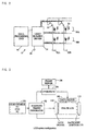
- a backlit display 20 comprises, generally, a backlight 22, a diffuser 24, and a light valve 26 (indicated by a bracket) that controls the transmittance of light from the backlight 22 to a user viewing an image displayed at the front of the panel 28.
- the light valve typically comprising a liquid crystal apparatus, is arranged to electronically control the transmittance of light for a picture element or pixel. Since liquid crystals do not emit light, an external source of light is necessary to create a visible image.
- the source of light for small and inexpensive LCDs, such as those used in digital clocks or calculators, may be light that is reflected from the back surface of the panel after passing through the panel.
- LCDs CMOS on silicon devices rely on light reflected from a backplane of the light valve to illuminate a display pixel.
- LCDs absorb a significant portion of the light passing through the assembly and an artificial source of light such as the backlight 22 comprising fluorescent light tubes or an array of light sources 30 (e.g., light-emitting diodes (LEDs), as illustrated in FIG. 1A and fluorescent tubes as illustrated in FIG. 1B ), are useful to produce pixels of sufficient intensity for highly visible images or to illuminate the display in poor lighting conditions.
- LEDs light-emitting diodes
- the light from the general point sources e.g., LEDS
- general line sources e.g., fluorescent tubes
- Light radiating from the light sources 30 of the backlight 22 comprises electromagnetic waves vibrating in random planes. Only those light waves vibrating in the plane of a polarizer's optical axis can pass through the polarizer.
- the light valve 26 includes a first polarizer 32 and a second polarizer 34 having optical axes arrayed at an angle so that normally light cannot pass through the series of polarizers. Images are displayable with an LCD because local regions of a liquid crystal layer 36 interposed between the first 32 and second 34 polarizer can be electrically controlled to alter the alignment of the plane of vibration of light relative of the optical axis of a polarizer and, thereby, modulate the transmittance of local regions of the panel corresponding to individual pixels 36 in an array of display pixels.
- the layer of liquid crystal molecules 36 occupies a cell gap having walls formed by surfaces of the first 32 and second 34 polarizers.
- the walls of the cell gap are rubbed to create microscopic grooves aligned with the optical axis of the corresponding polarizer.
- the grooves cause the layer of liquid crystal molecules adjacent to the walls of the cell gap to align with the optical axis of the associated polarizer.
- each successive molecule in the column of molecules spanning the cell gap will attempt to align with its neighbors.
- the result is a layer of liquid crystals comprising innumerable twisted columns of liquid crystal molecules that bridge the cell gap.
- a voltage is applied to a spatially corresponding electrode of a rectangular array of transparent electrodes deposited on a wall of the cell gap.
- the resulting electric field causes molecules of the liquid crystal adjacent to the electrode to rotate toward alignment with the field.
- the effect is to untwist the column of molecules so that the plane of vibration of the light is progressively rotated away from the optical axis of the polarizer as the field strength increases and the local transmittance of the light valve 26 is reduced.
- the pixel 28 progressively darkens until the maximum extinction of light 40 from the light source 42 is obtained.
- Color LCD displays are created by varying the intensity of transmitted light for each of a plurality of primary color elements (typically, red, green, and blue) elements making up a display pixel. Other arrangements of structures may likewise be used.
- the LCD uses transistors as a select switch for each pixel, and adopts a display method (hereinafter, called as a "hold-type display”), in which a displayed image is held for a frame period.
- a CRT hereinafter, called as an "impulse-type display”
- the darkened pixel is displayed between each frame of a motion image that is rewritten in 60 Hz in case of the impulse-type display like the CRT. That is, the black of the darkened pixel is displayed excluding a period when the image is displayed, and one frame of the motion image is presented respectively to the viewer as an independent image. Therefore, the image is observed as a clear motion image in the impulse-type display.
- the LCD is fundamentally different from CRT in time axis hold characteristic in an image display. Therefore, when the motion image is displayed on a LCD, image deterioration such as blurring the image is caused.
- image deterioration arises from a viewer that follows the moving object of the motion image (when the eyeball movement of the viewer is a following motion), even if the image is rewritten, for example, at 60 Hz discrete steps.
- the eyeball has a characteristic to attempt to smoothly follow the moving object even though it is discretely presented in a "hold type" manner.
- the displayed image of one frame of the motion image is held for one frame period, and is presented to the viewer during the corresponding period as a still image. Therefore, even though the eyeball of the viewer smoothly follows the moving object, the displayed image stands still for one frame period. Therefore, the shifted image is presented according to the speed of the moving object on the retina of the viewer. Accordingly, the image will appear blurred to the viewer due to integration by the eye. In addition, since the change between the images presented on the retina of the viewer increases with greater speed, such images become even more blurred.
- the backlight 22 comprises an array of locally controllable light sources 30.
- the individual light sources 30 of the backlight may be light-emitting diodes (LEDs), an arrangement of phosphors and lenses, or other suitable light-emitting devices.
- the backlight may include a set of independently controllable light sources, such as one or more cold cathode ray tubes.
- the light-emitting diodes may be 'white' and/or separate colored light emitting diodes so that the backlight array comprises a plurality of different colored lighting elements.
- the individual light sources 30 of the backlight array 22 are independently controllable to output light at a luminance level independent of the luminance level of light output by the other light sources so that a light source can be modulated in response to any suitable signal.
- a film or material may be overlaid on the backlight to achieve the spatial and/or temporal light modulation.
- the light sources 30 (LEDs illustrated) of the array 22 are typically arranged in the rows, for examples, rows 50A and 50 B, (indicated by brackets) and columns, for examples, columns 52A and 52bB (indicated by brackets) of a rectangular array.
- the output of the light sources 30 of the backlight are controlled by a backlight driver 53.
- the light sources 30 are driven by a light element driver 54 that powers the elements by selecting a column of elements 52 A or 52 B by actuating a column selection transistor 55 and connecting a selected light source 30 of the selected column to ground 56.
- a data processing unit 58 processing the digital values for pixels of an image to be displayed, provides a signal to the light driver 54 to select the appropriate light source 30 corresponding to the displayed pixel and to drive the light source with a power level to produce an appropriate level of illumination of the light source.
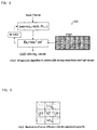
- FIG. 3 illustrates a block diagram of a typical data path within a liquid crystal panel.
- the video source (video data) 100 may be provided from any suitable source, such as for example, television broadcast, Internet connection, file server, digital video disc, computer, video on demand, or broadcast.
- the video source 100 is provided to a scanning and timing generator 102 where the video source is converted to a suitable format for presentation on the display.
- each line of data is provided to an overdrive 104, in combination with a frame buffer 106, to compensate for the slow temporal response of the display.
- the overdrive may be analog in nature, if desired.
- the signal from the overdrive 104 is preferably converted to a voltage value in the data driver 108 which is output to individual data electrodes of the display.
- the generator 102 also provides a clock signal to the gate driver 110, thereby selecting one row at a time, which stores the voltage data on the data electrode on the storage capacitor of each pixel of the display.
- the generator 102 also provides backlight control signals to backlight controller 112 to control the level of luminance from the backlight, and/or the color or color balance of the light provided in the case of spatially non-uniform backlight (e.g., based upon image content and/or spatially different in different regions of the 16 display).
- Liquid crystal displays have limited dynamic range due the extinction ratio of polarizers and imperfection of the liquid crystal material.
- a low resolution light emitting diode (LED) backlight system may be used to modulate the light that feeds into the liquid crystal material.
- LED typically has lower spatial resolution than the LCD. Due to the lower resolution LED, the high dynamic range display based on this technology can not display a high dynamic pattern of high spatial resolution. But it can display both very bright image (> 2000 cd/m 2 ) and very dark image ( ⁇ 0.5 cd/m 2 ) simultaneously.
- the inability to display high dynamic range of high spatial resolution is not a serious issue since the human eye has limited dynamic range in a local area, and with visual masking, the human eye can hardly perceive the limited dynamic range of high spatial frequency content.
- Figure 4 illustrates one previously existing technique, described in US2006/0103621 , to convert a high spatial resolution high dynamic range (HDR) image into a lower resolution light emitting diode (LED) image and a high resolution liquid crystal display image.
- the luminance is extracted from the HDR image.
- the extracted luminance is then low pass filtered and sub-sampled to the resolution of the LED array.
- the filtered and sub-sampled image may be processed to reduce cross talk effects.
- the cross-talk corrected image may be sent to a raster decoder and displayed on the LED layer of the HDR display.
- the desirable backlight image may be predicted by convolving an up-sampled LED image with the point spread function of LED.
- the LCD image is derived by dividing the original HDR image with predicted backlight image to obtain the simulated backlight. Since the final displayed image is the product of LED backlight image and the LCD transmittance, this approach reproduces the original HDR image.
- the resulting displayed images using this technique tends to have limited bright specular highlights that are limited in spatial extent. Accordingly, many HDR images contains specular highlight that are extremely bright, but very small in spatial extent, which may not be adequately represented on the display.
- the system may also use the maximum image (or some value associated with regions where a significant value exists) which is the local maximum in the HDR image divided by the max transmittance of LCD.
- the broad spread in the LED point spread function results in decreasing the potential contrast ratio of the image and also fails to minimize the power consumption of the display.
- a modified approach may be used to derive the LED driving value to achieve a higher contrast in the backlight image.
- the resulting higher contrast backlight image combining with the high resolution LCD image can produce much higher dynamic image to be displayed and also reduce the power consumption of the LED backlight.
- moving images tend to flicker more than expected, i.e. the fluctuation of display output.
- a particular configuration of the display namely a LCD combined with LED array
- the temporal response of the LCD layer is different than the LED array in a manner that may result in flickering.
- the LED has a much faster temporal response than the LCD layer.
- these errors resulting in flickering may be due to inaccuracies in the point spread function approximation, which may vary from display to display, and from LED to LED.
- the course nature of the LED array tends to result in course selection of the LED values, generally being on or off.
- FIG. 1 shows a schematic of a HDR display with LED layer as a backlight for a LCD.
- the light from array of LEDs passes through the diffusion layer and illuminates the LCD.
- the backlight image is further modulated by the LCD.
- the displayed image is the product of LED backlight and transmittance of LCD: T LCD (x, y).
- the dynamic range of display is the product of the dynamic range of LED and LCD.
- the notation may use normalized LCD and LED output limited to between 0 and 1.
- FIG. 5 shows an exemplary technique to convert (modify) a received HDR image 900 into a low resolution LED image 902 by providing modified data to the backlight array and a high resolution LCD image 904 by providing modified data to the light valve.
- the LCD resolution is m x n pixels with its range from 0 to 1, with 0 to be black and 1 to be the maximum transmittance.
- the LED resolution is M x N with M ⁇ m and N ⁇ n.
- a scaling or cropping step may be used to convert the HDR image to LCD image resolution.
- the HDR image such as in sRGB color space, may be linearized using a 1-dimensional look up table 901.
- the linearized HDR image is low pass filtered by the point spread function of the diffusion screen (or other function) and sub-sampled (down sample) to an intermediate resolution (M1xN1) 906.
- M1xN1 intermediate resolution
- One example of an intermediate resolution is eight times the LED resolution (8Mx8N).
- the extra resolution of the sub-sampled image may be used to reduce flickering that would occur as a result of moving objects over a series of frames of a video, and to preserve specular highlights.
- the additional data points in the LED matrix also permit a smoothing of the transition of the LED values when movement occurs in the image of a video.
- an adjacent LED for example, a second colored light element having a different color than the first colored lighting element
- the block maximum 912 (or other suitable value) is selected.
- the processing of each block may correspond to the intermediate resolution with some overlap between each block, i.e., the block size is (1+k)*(m/M x n/N), where k (i.e., 0.25) is the overlapping factor.
- the block maximum (or other suitable value) is used to form a LED max image (MxN) 914. It is to be understood that any suitable technique may be used to define the maximum (or other suitable value) for each location based upon the pixel location, region, and/or neighboring regions.
- the block mean 916 (or other suitable value) is selected. If desired, the processing of each block may correspond to the intermediate resolution with some overlap between each block, i.e., the block size is (1+k)*(m/M x n/N), where k (i.e., 0.25) is the overlapping factor.
- the mean value (or other suitable value) is used to form a LED mean image (MxN) 918.
- the mean image 918 may include a set of values at the dark portion of the range in a uniform area, then with the combination of a low backlight level the LCD tends to either be generally not transmissive or generally fully transmissive.
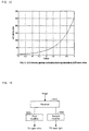
- a one-dimensional look up table 920 may be used that includes a dark region offset and non-linear expansion across its range to boost the values in the dark region, such as illustrated in FIG. 6 .
- This provides an offset mean tone-adjusted image 922. It is to be understood that any suitable technique may be used to define the mean (or other suitable value) for each location based upon the location, region, and/or neighboring regions.
- LED max 914 and LED mean 922 is selected 924. This larger value helps account for the fact that the low pass filtering tends to decrease the dynamic range that would otherwise have been rendered on the display. Taking into account the local maximum assists to preserve the specular highlights. If desired, for non specular highlight areas the system may increase the backlight levels, which is compensated by the LCD, to ensure operation toward the lower end of the LCD tone curve.
- the output of the max 924 is the target backlight level and its size may be the same as the number of active backlight blocks (M x N).
- intensity fluctuations generally referred to as flickering
- the object movement causes an abrupt change in the LED driving values.
- the change in backlight can be compensated by the LCD.
- the LCD due to timing differences between the LED and LCD, and the mismatch in the point-spread-function used in calculation of the compensation and the actual point spread function of the LED, there is some small intensity variations. Minor small intensity variations are frequently not objectionable. However, when the eye of a viewer is tracking an object, then the small backlight changes become a periodic objectionable fluctuation.
- the system may include a motion adaptive technique 925 to reduce the sudden LED change when an object moves across the LED grids.
- the motion adaptive technique 925 may use motion detection 926, which may be the classification of the video image into two classes, those regions with sufficient motion and those regions without sufficient motion.
- motion detection 926 may be the classification of the video image into two classes, those regions with sufficient motion and those regions without sufficient motion.
- the backlight contrast may be reduced so that there is less sudden changes in the LED driving value.
- the backlight contrast may be preserved to improve the contrast ratio and reduce power consumption.
- Motion detection may be performed at the subsampled image at M1xN1 resolution.
- the value at current frame may be compared to the corresponding block in the previous frame. If the difference is greater than a threshold, then the backlight block that contains this block is classified as motion block.
- each backlight block contains 8x8 sub-blocks.
- the process of motion detection may be as follows:
- LED max is the local max of LEDs in a window that centers on the current LED.
- a 3x3 window is a 3x3 window.
- a 5x5 window is another example.
- An alternative embodiment is using motion estimation.
- the window is aligned with the motion vector. This approach reduces the window size and preserves the contrast in the non motion direction, but the computation of motion vectors is more complex than motion detection.
- the LED may be of size M1 x N1 and range from 0 to 1. Since the PSF of the diffusion screen is typically larger than the LED spacing in order to provide a more uniform backlight image, there tends to be considerable crosstalk between the LED elements that are located close together.
- FIG. 7 shows a typical LED PSF where the PSF extends beyond the boarder of a particular LED.
- any LED has contribution from its entire neighboring LEDs.
- equation 2 can be used to calculate the backlight if given a LED driving signal, deriving LED driving signal to achieve a target backlight image is an inverse problem. This problem results in an ill posed de-convolution problem.
- a convolution kernel may be used to derive the LED driving signal, as shown in equation 3.
- the crosstalk correction kernel coefficients (c 1 and c 2 ) are negative to compensate for the crosstalk from neighboring LEDs.
- crosstalk c 2 c 1 c 2 c 1 c 0 c 1 c 2 c 1 c 2
- the crosstalk correction matrix does reduce the crosstalk effect from its immediate neighbors, but the resulting backlight image is still inaccurate with a low contrast. Another problem is that it produces many out of range driving values that have to be truncated which can result in more errors.
- the led driving value is derived so that backlight is larger than target luminance, i.e. led i j : led i j * psf x y ⁇ I x y
- Another feature is power saving so that the total LED output should be minimized or otherwise reduced.
- Flickering is due, at least in part, to the non-stationary response of the LED which combines with the mismatch between the LCD and LED.
- the mismatch can be either spatially or temporally. Flickering can be reduced by decreasing the total led output fluctuation as a point object move through the LED grid.
- led i j min ⁇ i , j led i j ⁇ ⁇ i , j led i ⁇ x 0 , j ⁇ y 0 where x 0 and y 0 is the distance from the center of the LED.
- the flickering can be further reduced by temporal IIR filtering.
- a computationally efficient technique to derive the backlight values that satisfy equations 6, 7, and 8 may involve the following steps:
- the preferred technique to derive the LED driving values ie. derive data provided to the backlight array - see block 927 of FIG. 5
- the preferred single pass technique is illustrated in FIG. 8 .
- the difference between the target backlight (BL) of the new frame and the backlight (BLi-1) of the previous frame is calculated.
- the backlight of the previous frame (BLi_i) is provided by a BL buffer.
- This difference may be scaled by a scale factor, such as a scale factor that ranges from 0.5 to 2.0 times the inverse of the sum of the PSF.
- the new driving value is the sum of the previous LED driving value (LEDi_i) which was data previously provided to the backlight array and the aforementioned scaled difference.
- the new data provided to the backlight (BLi) is then estimated by the convolution of the new LED driving value and the PSF of the LED.
- the derived LED value from the preferred single pass technique can be less than 0 and great than 1. Since the LED can only be driven between 0 (minimum) and 1 (maximum), these values should be truncated to the rage of 0 to 1. Truncation to 0 still satisfies equation 4, but truncation to 1 does not. This truncation causes a shortfall in the backlight. The shortfall to 1 may be compensated by increasing the driving value of its neighboring LEDs, such as illustrated in FIG. 9 . Accordingly, information related to the previous backlight illumination is used to select the next backlight level.
- a post processing technique may be used to diffuse this truncation error, such as follows:
- ErrWeight is the array for error diffusion coefficients based on the rank order.
- the errWeight [0.75 0.5 0.5 0.25], where the largest coefficient is for the neighboring LED with the lowest driving value, and the smallest coefficient is for the neighboring LED with the driving value.
- extra light is obtained by increasing the illumination of the LED(s) with less illumination, while simultaneously, decreasing the illumination from LCD(s) with greater illumination, such that the total illumination is substantially unchanged.
- a similar diffusion process may be used to diffuse the error to the corner neighbors to further increase the brightness of small objects.
- the LED driving values may be changed so that to reduce sudden backlight change in the dark region.
- the output of the halo reduction 928 results in the LED image 902 which may be provided to the LED driver circuit 930.
- the system looks in the neighborhood of the pixel. If there are bright pixel(s) in the neighborhood (ie. in at least one neighboring lighting element value in a neighborhood of light element values having a sufficiently large value), then the system may boost the dark spot based on the distance to the bright pixel(s). The closer to the bright pixel the greater the boost.
- the neighborhood of light element values includes at least one adjacent lighting element. It is also possible to include at least four adjacent lighting elements in the neighborhood of light element values.
- FIG. 11 shows the measured spectral of the blue (LCD) channel with both blue and green LED on.
- one of the blue and green LEDs is the first colored lighting element and the other is the second colored light element.
- the second peak at the wavelength of 520 nm is from the green LED.
- This crosstalk causes color shift which proportional to the product of green LED and blue LCD.
- the crosstalk from the green LED to the blue LCD may be reduced using a suitable technique.
- the technique shown in FIG. 12 involves (1) estimating the green backlight by a convolution of the green LED with the point-spread-function (PSF), (2) boosting the value of the blue weight (calculating the blue LED boost weight), (3) blurring the weighted map by convolving with a blur kernel, such as that shown in FIG. 12 , (4) increasing the blue LED based upon the value of the blue weight, and (5) reduce the green LCD to compensate for the blue filter leakage.
- the crosstalk from the green LED to the red LED; the blue LED to the green LCD; the blue LED to the red LCD; the red LED to the blue LCD; and the red LED to the green LCD may be reduced using a suitable technique.
- the LED image 902 may be up-sampled to the backlight predicted scale 940.
- This up-sampling predicted image may be convolved with the backlight element post spread function 942. Then this convolved data is up-sampled to the LCD sampling 944, to result in a backlight density.
- a one dimensional look-up-table may be used to convert linear luminance values into density values such as block 946 and 954 (ie. to convert from "substantially linear” data to "substantially non-linear” data).
- the LCD density may be derived by subtracting the backlight density 946 from the image density 954 to obtain the LCD density 956. In other words, a substantially non-linear data difference is the result.
- Another 1D LUT 948 may be used to convert the LCD density 956 into code value domain, as illustrated in FIG. 13 .
- Color halo correction 950 may be applied to the output of the 1D LUT 948 to obtain the LCD image 904.
- the LCD image 904 is provided to the LCD driver circuit 952 so that it is suitable to provide a desired illumination for the image.
- the above methods can be used with a liquid crystal display such as that shown in FIG. 14 .
- the liquid crystal display includes a backlight array of individually controllable lighting elements and a light valve corresponding to the individually controllable lighting elements.
- the display includes a receiver 1010 for receiving an image; a first modifier 1020 for modifying the image to provide data to the light valve; a second modifier 1030 for modifying the image to provide data to the backlight array, wherein the backlight array has a plurality of different colored lighting elements; wherein the data provided to the backlight array is based at least in part upon the constraint of modification of at least one of the value of a first colored element and the value of an adjacent second colored light element having a different color than the first colored lighting element to reduce the cross-talk between the first and second colored lighting elements; wherein the data provided to the light valve corresponding to the individually controllable lighting element is suitable to provide the desired illumination for the image.
Description
- The present invention relates to backlit displays and methods and, more particularly, to a backlit display with improved performance characteristics.
- The local transmittance of a liquid crystal display (LCD) panel or a liquid crystal on silicon (LCOS) display can be varied to modulate the intensity of light passing from a backlit source through an area of the panel to produce a pixel that can be displayed at a variable intensity. Whether light from the source passes through the panel to a viewer or is blocked is determined by the orientations of molecules of liquid crystals in a light valve.
- Since liquid crystals do not emit light, a visible display requires an external light source. Small and inexpensive LCD panels often rely on light that is reflected back toward the viewer after passing through the panel. Since the panel is not completely transparent, a substantial part of the light is absorbed during its transit of the panel and images displayed on this type of panel may be difficult to see except under the best lighting conditions. On the other hand, LCD panels used for computer displays and video screens are typically backlit with fluorescent tubes or arrays of light-emitting diodes (LEDs) that are built into the sides or back of the panel. To provide a display with a more uniform light level, light from these points or line sources is typically dispersed in a diffuser panel before impinging on the light valve that controls transmission to a viewer.
- The transmittance of the light valve is controlled by a layer of liquid crystals interposed between a pair of polarizers. Light from the source impinging on the first polarizer comprises electromagnetic waves vibrating in a plurality of planes. Only that portion of the light vibrating in the plane of the optical axis of a polarizer can pass through the polarizer. In an LCD, the optical axes of the first and second polarizers are arranged at an angle so that light passing through the first polarizer would normally be blocked from passing through the second polarizer in the series. However, a layer of the physical orientation of the molecules of liquid crystal can be controlled and the plane of vibration of light transiting the columns of molecules spanning the layer can be rotated to either align or not align with the optical axes of the polarizers. It is to be understood that normally white may likewise be used.
- The surfaces of the first and second polarizers forming the walls of the cell gap are grooved so that the molecules of liquid crystal immediately adjacent to the cell gap walls will align with the grooves and, thereby, be aligned with the optical axis of the respective polarizer. Molecular forces cause adjacent liquid crystal molecules to attempt to align with their neighbors with the result that the orientation of the molecules in the column spanning the cell gap twist over the length of the column. Likewise, the plane of vibration of light transiting the column of molecules will be "twisted" from the optical axis of the first polarizer to that of the second polarizer. With the liquid crystals in this orientation, light from the source can pass through the series polarizers of the translucent panel assembly to produce a lighted area of the display surface when viewed from the front of the panel. It is to be understood that the grooves may be omitted in some configurations.
- To darken a pixel and create an image, a voltage, typically controlled by a thin-film transistor, is applied to an electrode in an array of electrodes deposited on one wall of the cell gap. The liquid crystal molecules adjacent to the electrode are attracted by the field created by the voltage and rotate to align with the field. As the molecules of liquid crystal are rotated by the electric field, the column of crystals is "untwisted," and the optical axes of the crystals adjacent the cell wall arc rotated out of alignment with the optical axis of the corresponding polarizer progressively reducing the local transmittance of the light valve and the intensity of the corresponding display pixel. Color LCD displays are created by varying the intensity of transmitted light for each of a plurality of primary color elements (typically, red, green, and blue) that make up a display pixel.
- LCDs can produce bright, high resolution, color images and are thinner, lighter, and draw less power than cathode ray tubes (CRTs). As a result, LCD usage is pervasive for the displays of portable computers, digital clocks and watches, appliances, audio and video equipment, and other electronic devices. On the other hand, the use of LCDs in certain "high end markets," such as video and graphic arts, is frustrated, in part, by the limited performance of the display.
- What is desired, therefore, is a liquid crystal display having reduced blur.
-
US 2005/0231457 proposes a liquid crystal display apparatus that includes a liquid crystal display, a backlight unit for emitting rays of light of three or more colors, the ray of each color being controlled, and applying these rays of light onto the liquid crystal display. A controller is further provided for controlling a change of display data of each color of the liquid crystal display and an emitted light quantity of each color of the backlight unit at a time, based on a video signal being inputted for displaying the corresponding image and an output signal sent from an ambient light sensor for sensing ambient light. DocumentUS2006/0103621 discloses a method for displaying an image on a display device containing a liquid crystal light valve and a backlight including a plurality of light emitting elements. The input image signal is re-sampled to a lower resolution before determining the substantial maximum for one of the regions. The image signal to be provided to the backlight is modified based upon crosstalk. - A method for displaying an image on a liquid crystal display is defined by the appended
claim 1. - A liquid crystal display including a backlight array of individually controllable lighting elements and a light valve is defined by the appended
claim 3 - The foregoing and other objectives, features, and advantages of the invention will be more readily understood upon consideration of the following detailed description of the invention, taken in conjunction with the accompanying drawings.
-
-
FIGS. 1A and 1B are schematic diagrams of liquid crystal displays (LCDs); -
FIG. 2 is a schematic diagram of an exemplary driver for modulating the illumination of a plurality of light source elements of a backlight; -
FIG. 3 illustrates an exemplary LCD system configuration; -
FIG. 4 illustrates a high dynamic range image processing technique; -
FIG. 5 illustrates LED and LCD driving values; -
FIG. 6 illustrates tone mapping; -
FIG. 7 illustrates LED PSF; -
FIG. 8 illustrates a single pass LED driving scheme; -
FIG. 9 illustrates error diffusion; -
FIG. 10 illustrates a halo artifact; -
FIG. 11 illustrates color crosstalk; -
FIG. 12 illustrates a technique to reduce color crosstalk; -
FIG. 13 illustrates LCD inverse gamma correction; andFIG. 14 illustrates a LCD device for use with the methods of the present invention. - Referring to
FIG. 1A , abacklit display 20 comprises, generally, abacklight 22, adiffuser 24, and a light valve 26 (indicated by a bracket) that controls the transmittance of light from thebacklight 22 to a user viewing an image displayed at the front of thepanel 28. The light valve, typically comprising a liquid crystal apparatus, is arranged to electronically control the transmittance of light for a picture element or pixel. Since liquid crystals do not emit light, an external source of light is necessary to create a visible image. The source of light for small and inexpensive LCDs, such as those used in digital clocks or calculators, may be light that is reflected from the back surface of the panel after passing through the panel. Likewise, liquid crystal on silicon (LCOS) devices rely on light reflected from a backplane of the light valve to illuminate a display pixel. However, LCDs absorb a significant portion of the light passing through the assembly and an artificial source of light such as thebacklight 22 comprising fluorescent light tubes or an array of light sources 30 (e.g., light-emitting diodes (LEDs), as illustrated inFIG. 1A and fluorescent tubes as illustrated inFIG. 1B ), are useful to produce pixels of sufficient intensity for highly visible images or to illuminate the display in poor lighting conditions. There may not be alight source 30 for each pixel of the display and, therefore, the light from the general point sources (e.g., LEDS) or general line sources (e.g., fluorescent tubes) is typically dispersed by adiffuser panel 24 so that the lighting of the front surface of thepanel 28 is more uniform. - Light radiating from the
light sources 30 of thebacklight 22 comprises electromagnetic waves vibrating in random planes. Only those light waves vibrating in the plane of a polarizer's optical axis can pass through the polarizer. Thelight valve 26 includes afirst polarizer 32 and asecond polarizer 34 having optical axes arrayed at an angle so that normally light cannot pass through the series of polarizers. Images are displayable with an LCD because local regions of aliquid crystal layer 36 interposed between the first 32 and second 34 polarizer can be electrically controlled to alter the alignment of the plane of vibration of light relative of the optical axis of a polarizer and, thereby, modulate the transmittance of local regions of the panel corresponding toindividual pixels 36 in an array of display pixels. - The layer of
liquid crystal molecules 36 occupies a cell gap having walls formed by surfaces of the first 32 and second 34 polarizers. The walls of the cell gap are rubbed to create microscopic grooves aligned with the optical axis of the corresponding polarizer. The grooves cause the layer of liquid crystal molecules adjacent to the walls of the cell gap to align with the optical axis of the associated polarizer. As a result of molecular forces, each successive molecule in the column of molecules spanning the cell gap will attempt to align with its neighbors. The result is a layer of liquid crystals comprising innumerable twisted columns of liquid crystal molecules that bridge the cell gap. Aslight 40 originating at alight source element 42 and passing through thefirst polarizer 32 passes through each translucent molecule of a column of liquid crystals, its plane of vibration is twisted so that when the light reaches the far side of the cell gap its plane of vibration will be aligned with the optical axis of thesecond polarizer 34. The light 44 vibrating in the plane of the optical axis of thesecond polarizer 34 can pass through the second polarizer to produce a lightedpixel 38 at the front surface of thedisplay 28. - To darken the
pixel 28, a voltage is applied to a spatially corresponding electrode of a rectangular array of transparent electrodes deposited on a wall of the cell gap. The resulting electric field causes molecules of the liquid crystal adjacent to the electrode to rotate toward alignment with the field. The effect is to untwist the column of molecules so that the plane of vibration of the light is progressively rotated away from the optical axis of the polarizer as the field strength increases and the local transmittance of thelight valve 26 is reduced. As the transmittance of thelight valve 26 is reduced, thepixel 28 progressively darkens until the maximum extinction of light 40 from thelight source 42 is obtained. Color LCD displays are created by varying the intensity of transmitted light for each of a plurality of primary color elements (typically, red, green, and blue) elements making up a display pixel. Other arrangements of structures may likewise be used. - The LCD uses transistors as a select switch for each pixel, and adopts a display method (hereinafter, called as a "hold-type display"), in which a displayed image is held for a frame period. In contrast, a CRT (hereinafter, called as an "impulse-type display") includes selected pixel that is darkened immediately after the selection of the pixel. The darkened pixel is displayed between each frame of a motion image that is rewritten in 60 Hz in case of the impulse-type display like the CRT. That is, the black of the darkened pixel is displayed excluding a period when the image is displayed, and one frame of the motion image is presented respectively to the viewer as an independent image. Therefore, the image is observed as a clear motion image in the impulse-type display. Thus, the LCD is fundamentally different from CRT in time axis hold characteristic in an image display. Therefore, when the motion image is displayed on a LCD, image deterioration such as blurring the image is caused. The principal cause of this blurring effect arises from a viewer that follows the moving object of the motion image (when the eyeball movement of the viewer is a following motion), even if the image is rewritten, for example, at 60 Hz discrete steps. The eyeball has a characteristic to attempt to smoothly follow the moving object even though it is discretely presented in a "hold type" manner.
- In the hold-type display, the displayed image of one frame of the motion image is held for one frame period, and is presented to the viewer during the corresponding period as a still image. Therefore, even though the eyeball of the viewer smoothly follows the moving object, the displayed image stands still for one frame period. Therefore, the shifted image is presented according to the speed of the moving object on the retina of the viewer. Accordingly, the image will appear blurred to the viewer due to integration by the eye. In addition, since the change between the images presented on the retina of the viewer increases with greater speed, such images become even more blurred.
- In the
backlit display 20, thebacklight 22 comprises an array of locally controllablelight sources 30. The individuallight sources 30 of the backlight may be light-emitting diodes (LEDs), an arrangement of phosphors and lenses, or other suitable light-emitting devices. In addition, the backlight may include a set of independently controllable light sources, such as one or more cold cathode ray tubes. The light-emitting diodes may be 'white' and/or separate colored light emitting diodes so that the backlight array comprises a plurality of different colored lighting elements. The individuallight sources 30 of thebacklight array 22 are independently controllable to output light at a luminance level independent of the luminance level of light output by the other light sources so that a light source can be modulated in response to any suitable signal. Similarly, a film or material may be overlaid on the backlight to achieve the spatial and/or temporal light modulation. - Referring to
FIG. 2 , the light sources 30 (LEDs illustrated) of thearray 22 are typically arranged in the rows, for examples,rows columns 52A and 52bB (indicated by brackets) of a rectangular array. The output of thelight sources 30 of the backlight are controlled by abacklight driver 53. Thelight sources 30 are driven by alight element driver 54 that powers the elements by selecting a column ofelements column selection transistor 55 and connecting a selectedlight source 30 of the selected column to ground 56. Adata processing unit 58, processing the digital values for pixels of an image to be displayed, provides a signal to thelight driver 54 to select the appropriatelight source 30 corresponding to the displayed pixel and to drive the light source with a power level to produce an appropriate level of illumination of the light source. -
FIG. 3 illustrates a block diagram of a typical data path within a liquid crystal panel. The video source (video data) 100 may be provided from any suitable source, such as for example, television broadcast, Internet connection, file server, digital video disc, computer, video on demand, or broadcast. Thevideo source 100 is provided to a scanning andtiming generator 102 where the video source is converted to a suitable format for presentation on the display. In many cases, each line of data is provided to anoverdrive 104, in combination with aframe buffer 106, to compensate for the slow temporal response of the display. The overdrive may be analog in nature, if desired. The signal from theoverdrive 104 is preferably converted to a voltage value in thedata driver 108 which is output to individual data electrodes of the display. Thegenerator 102 also provides a clock signal to thegate driver 110, thereby selecting one row at a time, which stores the voltage data on the data electrode on the storage capacitor of each pixel of the display. Thegenerator 102 also provides backlight control signals tobacklight controller 112 to control the level of luminance from the backlight, and/or the color or color balance of the light provided in the case of spatially non-uniform backlight (e.g., based upon image content and/or spatially different in different regions of the 16 display). - Liquid crystal displays have limited dynamic range due the extinction ratio of polarizers and imperfection of the liquid crystal material. In order to display high dynamic images, a low resolution light emitting diode (LED) backlight system may be used to modulate the light that feeds into the liquid crystal material. By the combination of LED and LCD, a very high dynamic range display can be achieved. For cost reasons, the LED typically has lower spatial resolution than the LCD. Due to the lower resolution LED, the high dynamic range display based on this technology can not display a high dynamic pattern of high spatial resolution. But it can display both very bright image (> 2000 cd/m2) and very dark image (< 0.5 cd/m2) simultaneously. The inability to display high dynamic range of high spatial resolution is not a serious issue since the human eye has limited dynamic range in a local area, and with visual masking, the human eye can hardly perceive the limited dynamic range of high spatial frequency content.
-
Figure 4 illustrates one previously existing technique, described inUS2006/0103621 , to convert a high spatial resolution high dynamic range (HDR) image into a lower resolution light emitting diode (LED) image and a high resolution liquid crystal display image. The luminance is extracted from the HDR image. The extracted luminance is then low pass filtered and sub-sampled to the resolution of the LED array. The filtered and sub-sampled image may be processed to reduce cross talk effects. The cross-talk corrected image may be sent to a raster decoder and displayed on the LED layer of the HDR display. - The desirable backlight image may be predicted by convolving an up-sampled LED image with the point spread function of LED. The LCD image is derived by dividing the original HDR image with predicted backlight image to obtain the simulated backlight. Since the final displayed image is the product of LED backlight image and the LCD transmittance, this approach reproduces the original HDR image. Unfortunately, the resulting displayed images using this technique tends to have limited bright specular highlights that are limited in spatial extent. Accordingly, many HDR images contains specular highlight that are extremely bright, but very small in spatial extent, which may not be adequately represented on the display.
- It was determined that the low pass filtering process smears this specular highlight causing the corresponding LED to have a lower value. Traditionally it would have been thought that any of the spatial details lost in the low pass filtering process could be recovered in the division operation. Although any spatial details lost in the filtering step can be theoretically recovered in the LCD image via the division operation, it turns out that the LCD can not recover the bright specular highlight due to its limited range (its transmittance can not exceed 1). Thus specular highlights are lost in the final display image although the HDR is capable of displaying that bright highlight.
- It was also determined that the low pass filtering works well for regions of the image that are not at the extremes of brightness and darkness. Accordingly, another criteria may be used to account for those regions where the low pass filtering is not exceptionally effective. In addition to using the low pass filtered image to derive the LED image, the system may also use the maximum image (or some value associated with regions where a significant value exists) which is the local maximum in the HDR image divided by the max transmittance of LCD.
- In addition, it was determined that the broad spread in the LED point spread function (PSF), results in decreasing the potential contrast ratio of the image and also fails to minimize the power consumption of the display. In order to improve the contrast ratio a modified approach may be used to derive the LED driving value to achieve a higher contrast in the backlight image. The resulting higher contrast backlight image combining with the high resolution LCD image can produce much higher dynamic image to be displayed and also reduce the power consumption of the LED backlight.
- Upon yet further investigation, moving images tend to flicker more than expected, i.e. the fluctuation of display output. After consideration of a particular configuration of the display, namely a LCD combined with LED array, it was determined that the temporal response of the LCD layer is different than the LED array in a manner that may result in flickering. In general, the LED has a much faster temporal response than the LCD layer. In addition, these errors resulting in flickering may be due to inaccuracies in the point spread function approximation, which may vary from display to display, and from LED to LED. In addition, the course nature of the LED array tends to result in course selection of the LED values, generally being on or off.
-
FIG. 1 shows a schematic of a HDR display with LED layer as a backlight for a LCD. The light from array of LEDs passes through the diffusion layer and illuminates the LCD. The backlight image is given by:
- The displayed image is the product of LED backlight and transmittance of LCD: TLCD(x, y).

- By combining the LED and LCD, the dynamic range of display is the product of the dynamic range of LED and LCD. For simplicity, the notation may use normalized LCD and LED output limited to between 0 and 1.
-
FIG. 5 shows an exemplary technique to convert (modify) a receivedHDR image 900 into a lowresolution LED image 902 by providing modified data to the backlight array and a highresolution LCD image 904 by providing modified data to the light valve. The LCD resolution is m x n pixels with its range from 0 to 1, with 0 to be black and 1 to be the maximum transmittance. The LED resolution is M x N with M < m and N < n. For simplicity it may be assumed that the HDR image has the same resolution as LCD. If HDR image is of different resolution, a scaling or cropping step may be used to convert the HDR image to LCD image resolution. - The HDR image, such as in sRGB color space, may be linearized using a 1-dimensional look up table 901. The linearized HDR image is low pass filtered by the point spread function of the diffusion screen (or other function) and sub-sampled (down sample) to an intermediate resolution (M1xN1) 906. One example of an intermediate resolution is eight times the LED resolution (8Mx8N). The extra resolution of the sub-sampled image may be used to reduce flickering that would occur as a result of moving objects over a series of frames of a video, and to preserve specular highlights. The additional data points in the LED matrix also permit a smoothing of the transition of the LED values when movement occurs in the image of a video. This facilitates one LED (for example, a first color lighting element) to gradually decrease in value as an adjacent LED (for example, a second colored light element having a different color than the first colored lighting element) gradually increases in value, which reduces the resulting flickering of the image that would result if the changes were more abrupt. By using this form of "constraint of motion", the cross talk between the first and second colored lighting elements can be reduced.
- For each block of pixels of the low-pass filtered
sub-sampled image 910 the block maximum 912 (or other suitable value) is selected. If desired, the processing of each block may correspond to the intermediate resolution with some overlap between each block, i.e., the block size is (1+k)*(m/M x n/N), where k (i.e., 0.25) is the overlapping factor. For each block, the block maximum (or other suitable value) is used to form a LEDmax image (MxN) 914. It is to be understood that any suitable technique may be used to define the maximum (or other suitable value) for each location based upon the pixel location, region, and/or neighboring regions. - For each block of pixels of the low-pass filtered
sub-sampled image 910 the block mean 916 (or other suitable value) is selected. If desired, the processing of each block may correspond to the intermediate resolution with some overlap between each block, i.e., the block size is (1+k)*(m/M x n/N), where k (i.e., 0.25) is the overlapping factor. For each block, the mean value (or other suitable value) is used to form a LEDmean image (MxN) 918. Themean image 918 may include a set of values at the dark portion of the range in a uniform area, then with the combination of a low backlight level the LCD tends to either be generally not transmissive or generally fully transmissive. Having the LCD operate at its extremes tends to appear noisy with a noisy input. To enhance themean image 918 to reduce its resulting visual noise a one-dimensional look up table 920 may be used that includes a dark region offset and non-linear expansion across its range to boost the values in the dark region, such as illustrated inFIG. 6 . This provides an offset mean tone-adjustedimage 922. It is to be understood that any suitable technique may be used to define the mean (or other suitable value) for each location based upon the location, region, and/or neighboring regions. - From these two
LED images LED max 914 andLED mean 922 is selected 924. This larger value helps account for the fact that the low pass filtering tends to decrease the dynamic range that would otherwise have been rendered on the display. Taking into account the local maximum assists to preserve the specular highlights. If desired, for non specular highlight areas the system may increase the backlight levels, which is compensated by the LCD, to ensure operation toward the lower end of the LCD tone curve. - The output of the
max 924 is the target backlight level and its size may be the same as the number of active backlight blocks (M x N). As previously noted, intensity fluctuations, generally referred to as flickering, may be observed when an object moves across LED boundaries. The object movement causes an abrupt change in the LED driving values. Theoretically, the change in backlight can be compensated by the LCD. But due to timing differences between the LED and LCD, and the mismatch in the point-spread-function used in calculation of the compensation and the actual point spread function of the LED, there is some small intensity variations. Minor small intensity variations are frequently not objectionable. However, when the eye of a viewer is tracking an object, then the small backlight changes become a periodic objectionable fluctuation. The frequency of the fluctuation is the product of the video frame rate and object motion speed in terms of LED blocks per frame. If an object moves across a LED block in 8 video frames and the video frame rate is 60 Hz, the flickering frequency is 60 hz * 0.125=7.5 Hz. This is about at the peak of the human visual sensitivity to flickering and it makes a very annoying artifact. To reduce this motion flickering, the system may include a motionadaptive technique 925 to reduce the sudden LED change when an object moves across the LED grids. - The motion
adaptive technique 925 may usemotion detection 926, which may be the classification of the video image into two classes, those regions with sufficient motion and those regions without sufficient motion. In the motion region, the backlight contrast may be reduced so that there is less sudden changes in the LED driving value. In the insufficient motion region, the backlight contrast may be preserved to improve the contrast ratio and reduce power consumption. - Motion detection may be performed at the subsampled image at M1xN1 resolution. The value at current frame may be compared to the corresponding block in the previous frame. If the difference is greater than a threshold, then the backlight block that contains this block is classified as motion block. In the preferred embodiment, each backlight block contains 8x8 sub-blocks. The process of motion detection may be as follows:
- For each frame:
- (1) Calculate the average of each sub-block in the input image for the current frame.
- (2) If the difference between the average in this frame and the sub-block average of the previous frame is greater than a threshold (such as 5% of total range), then backlight block that contains the sub-block is a motion block. Thus a first motion map is formed.
- (3) Perform a morphological dilation operation on the motion map (change the still blocks neighboring to a motion block to motion block) to form a second enlarged motion map.
- (4) For each backlight block, the motion status map is updated based on the motion detection results:
- (i) if it is motion block, mMap(i,j)=min(4, mMap (i,j)+1);
- (ii) else (still block) mMap (i,j)=max(0, mMap (i,j)-1).
- The LED driving value is given by

- Where LEDmax is the local max of LEDs in a window that centers on the current LED. One example is a 3x3 window. Another example is a 5x5 window.
- An alternative embodiment is using motion estimation. The window is aligned with the motion vector. This approach reduces the window size and preserves the contrast in the non motion direction, but the computation of motion vectors is more complex than motion detection.
- Since the PSF of LED is larger than the LED spacing to provide a more uniform backlight image, there is considerable crosstalk between the LED elements that are located close together. The LED may be of size M1 x N1 and range from 0 to 1. Since the PSF of the diffusion screen is typically larger than the LED spacing in order to provide a more uniform backlight image, there tends to be considerable crosstalk between the LED elements that are located close together.
FIG. 7 shows a typical LED PSF where the PSF extends beyond the boarder of a particular LED. - Because of the PSF of the diffusion screen, any LED has contribution from its entire neighboring LEDs. Although
equation 2 can be used to calculate the backlight if given a LED driving signal, deriving LED driving signal to achieve a target backlight image is an inverse problem. This problem results in an ill posed de-convolution problem. Traditionally, a convolution kernel may be used to derive the LED driving signal, as shown inequation 3. The crosstalk correction kernel coefficients (c1 and c2) are negative to compensate for the crosstalk from neighboring LEDs.
- The crosstalk correction matrix does reduce the crosstalk effect from its immediate neighbors, but the resulting backlight image is still inaccurate with a low contrast. Another problem is that it produces many out of range driving values that have to be truncated which can result in more errors.
- Since the LCD output can not be more than 1, the led driving value is derived so that backlight is larger than target luminance, i.e.

- The syntax uses ":" to denote the constraint to achieve the desired LED values of the function in the curly bracket. Because of the limited contrast ratio (CR) due to leakage, LCD(x,y) generally can no longer reach 0. The solution is that when target value is smaller than LCD leakage, the led value is reduced to reproduce the dark luminance.

- Another feature is power saving so that the total LED output should be minimized or otherwise reduced.

- Flickering is due, at least in part, to the non-stationary response of the LED which combines with the mismatch between the LCD and LED. The mismatch can be either spatially or temporally. Flickering can be reduced by decreasing the total led output fluctuation as a point object move through the LED grid.

- A computationally efficient technique to derive the backlight values that satisfy equations 6, 7, and 8 may involves the following steps:
- (1) A single pass technique to derive the LED driving values with a constraint that led > 0.
- (2) Post-processing: for those LED with driving value more than a (maximum), threshold those values to 1 (or other suitable value) and then using an error diffusion technique distribute the error to its neighboring LEDs.
- While an iterative technique may be used, the preferred technique to derive the LED driving values (ie. derive data provided to the backlight array -
see block 927 ofFIG. 5 ) is non-iterative, and thus more computationally efficient. The preferred single pass technique is illustrated inFIG. 8 . The difference between the target backlight (BL) of the new frame and the backlight (BLi-1) of the previous frame is calculated. The backlight of the previous frame (BLi_i) is provided by a BL buffer. This difference may be scaled by a scale factor, such as a scale factor that ranges from 0.5 to 2.0 times the inverse of the sum of the PSF. The new driving value (LED) is the sum of the previous LED driving value (LEDi_i) which was data previously provided to the backlight array and the aforementioned scaled difference. The new data provided to the backlight (BLi) is then estimated by the convolution of the new LED driving value and the PSF of the LED. - The derived LED value from the preferred single pass technique can be less than 0 and great than 1. Since the LED can only be driven between 0 (minimum) and 1 (maximum), these values should be truncated to the rage of 0 to 1. Truncation to 0 still satisfies
equation 4, but truncation to 1 does not. This truncation causes a shortfall in the backlight. The shortfall to 1 may be compensated by increasing the driving value of its neighboring LEDs, such as illustrated inFIG. 9 . Accordingly, information related to the previous backlight illumination is used to select the next backlight level. - A post processing technique may be used to diffuse this truncation error, such as follows:
- (1) For these led i,j>1.
- (2) tmpVal=led i,j -1.
- (3) Set led i,j = 1.
- (4) Sort the 4 neighboring LEDs to ascending order.
- (5) If(max-min < min(diffThd, tmpVal/2)
- All the neighbor LEDs are increased by tmpVal/ 2.
- (6) Else
- They are increased by errWeight*tmpVal*2.
- ErrWeight is the array for error diffusion coefficients based on the rank order. In the preferred embodiment, the errWeight=[0.75 0.5 0.5 0.25], where the largest coefficient is for the neighboring LED with the lowest driving value, and the smallest coefficient is for the neighboring LED with the driving value. In general, extra light is obtained by increasing the illumination of the LED(s) with less illumination, while simultaneously, decreasing the illumination from LCD(s) with greater illumination, such that the total illumination is substantially unchanged.
- A similar diffusion process may be used to diffuse the error to the corner neighbors to further increase the brightness of small objects.
- Since the LED resolution is much lower than that of LCD, there are considerable amounts of spread in the LED PSF. If there is a sharp transition in the original image, the backlight for the dark region is considerably higher than needed, thus LCD layer may compensate. There are at least two problems with the compensation: (1) limited contrast ratio prevents an exact compensation, and (2) even if the compensation works well for normal viewing, it will not tend to work well at oblique viewing angles due to the angular dependence of the LCD transmittance. This mismatch between LED backlight and LCD may result in an undesirable halo artifact, as illustrated in
FIG. 10 . - To avoid or reduce this halo artifact (block 928 of
FIG. 5 ), the LED driving values may be changed so that to reduce sudden backlight change in the dark region. The output of thehalo reduction 928 results in theLED image 902 which may be provided to theLED driver circuit 930.
    If led(i,j) < Halo_low
         For(1=-halo_size_x: halo_size_x)
              For(k=halo_size_y:halo_size_y)
                   If(led(i-k,j-1)> halo_high)
                        d=sqrt(1*1+k*k)
                        Led(I,j)=led(I,j)+halo_blur(d)
                   End
              End
         End
   End
Claims (3)
- A method for displaying an image on a liquid crystal display including a backlight array (22) of individually controllable lighting elements (30) and a light valve (26) corresponding to said individually controllable lighting elements (30), a resolution of the backlight array being M x N and a resolution of the light valve being m x n where M < m and N < n, said individually controllable lighting elements (30) comprising at least a first colored lighting element and an adjacent second colored lighting element having a different color to said first colored lighting element, the method comprising:(a) receiving an image;(b) modifying said image to provide data to said light valve; and(c) modifying said image to provide data to said backlight array (22), wherein said backlight array has a plurality of different colored lighting elements;
wherein modifying said image to provide data to said backlight array (22) comprises generating a modified image by:(i) low pass filtering said received image (900),(ii) modifying said low pass filtered image so as to reduce cross-talk between said first colored lighting element and said adjacent second colored lighting element by subsampling said low pass filtered image to a resolution intermediate between the resolution of said backlight array (22) and the resolution of said light valve (26),(iii) selecting, for each of M x N blocks of pixels of the subsampled image, a maximum pixel value of the block and forming a first image from the maximum pixel values of the blocks,selecting, for each of the M x N blocks of pixels of the subsampled image, a mean pixel value of the block and forming a second image from the mean pixel values of the blocks,and, for each block of the M x N blocks, selecting the larger value of the first image and the second image, and(iv) if a lighting element value is below a threshold and at least one neighbouring lighting element value is sufficiently large, increasing the value of said lighting element value below said threshold, based on the distance to said one neighbouring lighting element such that the closer said one neighbouring lighting element, the greater the increase;and providing said modified image to said backlight array;and wherein modifying said image to provide data to said light valve comprises up-sampling said modified image to the resolution of the light valve, obtaining a light valve image (956) by dividing said received image (900) by said up-sampled image, and providing said light valve image (956) to said light valve (26). - The method of claim 1 wherein one of the said first and second colored light elements is a green LED and said data provided to said backlight array includes a convolution of the value of the green LED with a point-spread-function of a diffuser, the diffuser being provided between the backlight array (22) and the light valve (26).
- A liquid crystal display including a backlight array (22) of individually controllable lighting elements (30) and a light valve (26) corresponding to said individually controllable lighting elements (30), a resolution of the backlight array being M x N and a resolution of the light valve being m x n where M < m and N < n, wherein said individually controllable lighting elements (30) comprise at least a first colored lighting element and an adjacent second colored lighting element having a different color than said first colored lighting element, the liquid crystal display comprising:a receiver (1010) for receiving an image;a first modifier (1020) for modifying said image to provide data to said light valve;a second modifier (1030) for modifying said image to provide data to said backlight array (22), wherein said backlight array has a plurality of different colored lighting elements;wherein said second modifier (1030) is configured to generate a modified image by:(i) low pass filtering said received image,(ii) modifing said low pass filtered image by subsampling said low pass filtered image to a resolution intermediate between the resolution of said backlight array (22) and the resolution of said light valve (26) thereby to reduce the cross-talk between said first colored lighting element and said adjacent second colored light element having a different color than said first colored lighting element,(iii) select, for each of M x N blocks of pixels of the subsampled image, a maximum pixel value of the block and form a first image from the maximum pixel values of the blocks,
select, for each of the M x N blocks of pixels of the subsampled image, a mean pixel value of the block and form a second image from the mean pixel values of the blocks,
and, for each of the M x N blocks, select the larger value of the first image and the second image, and(iv) if a lighting element value is below a threshold and at least one neighbouring lighting element value is sufficiently large, increase the value of said lighting element value below said threshold, based on the distance to said one neighbouring lighting element such that the closer said one neighbouring lighting element, the greater the increase;and provide said modified image to said backlight array (22) as said data provided to said backlight array (22); andwherein said first modifier (1020) is configured to up-sample said modified image to the resolution of the light valve, obtain a light valve image (956) by dividing said received image (900) by said up-sampled image, and provide said light valve image (956) to said light valve (26) as said data provided to said light valve.
Applications Claiming Priority (2)
| Application Number | Priority Date | Filing Date | Title |
|---|---|---|---|
| US12/383,194 US8624824B2 (en) | 2009-03-19 | 2009-03-19 | Area adaptive backlight with reduced color crosstalk |
| PCT/JP2010/052576 WO2010106872A1 (en) | 2009-03-19 | 2010-02-15 | Area adaptive backlight display and method with reduced computation and halo artifacts |
Publications (3)
| Publication Number | Publication Date |
|---|---|
| EP2409194A1 EP2409194A1 (en) | 2012-01-25 |
| EP2409194A4 EP2409194A4 (en) | 2012-08-08 |
| EP2409194B1 true EP2409194B1 (en) | 2016-11-30 |
Family
ID=42737149
Family Applications (1)
| Application Number | Title | Priority Date | Filing Date |
|---|---|---|---|
| EP10753367.1A Not-in-force EP2409194B1 (en) | 2009-03-19 | 2010-02-15 | Area adaptive backlight display and method with reduced computation and halo artifacts |
Country Status (7)
| Country | Link |
|---|---|
| US (1) | US8624824B2 (en) |
| EP (1) | EP2409194B1 (en) |
| JP (1) | JP5568088B2 (en) |
| CN (2) | CN102334062B (en) |
| BR (1) | BRPI1008681A2 (en) |
| RU (1) | RU2489746C2 (en) |
| WO (1) | WO2010106872A1 (en) |
Families Citing this family (20)
| Publication number | Priority date | Publication date | Assignee | Title |
|---|---|---|---|---|
| US8537098B2 (en) * | 2009-08-05 | 2013-09-17 | Dolby Laboratories Licensing Corporation | Retention and other mechanisms or processes for display calibration |
| GB2475026A (en) * | 2009-08-07 | 2011-05-11 | Alessandro Artusi | Display for displaying digital images having improved contrast ratio |
| US8947339B2 (en) * | 2009-12-21 | 2015-02-03 | Sharp Laboratories Of America, Inc. | Noise-compensated LCD display |
| EP2583272B1 (en) * | 2010-06-21 | 2016-01-20 | Dolby Laboratories Licensing Corporation | Displaying images on local-dimming displays |
| US9030466B2 (en) * | 2010-10-05 | 2015-05-12 | Empire Technology Development Llc | Generation of depth data based on spatial light pattern |
| US8687143B2 (en) * | 2010-12-20 | 2014-04-01 | Sharp Laboratories Of America, Inc. | Multi-primary display with area active backlight |
| EP2862162B1 (en) * | 2012-06-15 | 2020-03-18 | Dolby Laboratories Licensing Corporation | Systems and methods for controlling dual modulation displays |
| WO2015088963A1 (en) * | 2013-12-11 | 2015-06-18 | Robert Bosch Gmbh | Miter saw including a chain drive |
| KR20160102438A (en) * | 2013-12-27 | 2016-08-30 | 톰슨 라이센싱 | Method and device for tone-mapping a high dynamic range image |
| US20150228219A1 (en) * | 2014-02-12 | 2015-08-13 | Dolby Laboratories Licensing Corporation | Dual Modulator Synchronization in a High Dynamic Range Display System |
| CN111929963B (en) * | 2014-09-16 | 2023-05-09 | Ipg光子公司 | Broadband red light generator for RBG display |
| US20160284265A1 (en) * | 2015-03-26 | 2016-09-29 | Emagin Corporation | Method of Implementing Global Illumination With OLED Displays |
| JP6711564B2 (en) | 2015-06-26 | 2020-06-17 | キヤノン株式会社 | Display device, control method thereof, and program |
| US9858872B2 (en) | 2015-07-15 | 2018-01-02 | Htc Corporation | Electronic device and control method |
| JP7054851B2 (en) | 2016-09-09 | 2022-04-15 | パナソニックIpマネジメント株式会社 | Display device and signal processing method |
| CN106782231B (en) * | 2017-01-20 | 2020-09-11 | 合肥安达创展科技股份有限公司 | Animation display system based on LCD light valve array |
| FR3101691B1 (en) * | 2019-10-04 | 2022-07-08 | Valeo Vision | METHOD FOR CONTROLLING A LIGHT DEVICE FOR THE EMISSION OF A PIXELIZED LIGHT BEAM |
| CN111798805A (en) * | 2020-07-29 | 2020-10-20 | 北京显芯科技有限公司 | Backlight processing system, apparatus, method, backlight driver and storage medium |
| US11887518B2 (en) * | 2022-01-06 | 2024-01-30 | Sharp Kabushiki Kaisha | Display device having displayable area expansion unit and cutting unit and control method thereof |
| US11856311B1 (en) * | 2022-08-25 | 2023-12-26 | Aspinity, Inc. | Motion detection based on analog video stream |
Citations (1)
| Publication number | Priority date | Publication date | Assignee | Title |
|---|---|---|---|---|
| US20060103621A1 (en) * | 2004-11-16 | 2006-05-18 | Sharp Laboratories Of America, Inc. | Technique that preserves specular highlights |
Family Cites Families (24)
| Publication number | Priority date | Publication date | Assignee | Title |
|---|---|---|---|---|
| US4631691A (en) * | 1984-05-14 | 1986-12-23 | Rca Corporation | Video display device simulation apparatus and method |
| JPH0277659A (en) * | 1988-09-13 | 1990-03-16 | Nec Corp | Circuit for measuring signal-to-noise ratio |
| TW225025B (en) * | 1992-10-09 | 1994-06-11 | Tektronix Inc | |
| US6809741B1 (en) * | 1999-06-09 | 2004-10-26 | International Business Machines Corporation | Automatic color contrast adjuster |
| JP2002077659A (en) | 2000-09-05 | 2002-03-15 | Konica Corp | Method and apparatus to attain favorite color conversion |
| US7320531B2 (en) * | 2003-03-28 | 2008-01-22 | Philips Lumileds Lighting Company, Llc | Multi-colored LED array with improved brightness profile and color uniformity |
| CN1771518A (en) * | 2003-04-09 | 2006-05-10 | 皇家飞利浦电子股份有限公司 | Generation of motion blur |
| JP3701661B2 (en) * | 2003-12-05 | 2005-10-05 | シャープ株式会社 | Display panel and display device |
| JP4612406B2 (en) * | 2004-02-09 | 2011-01-12 | 株式会社日立製作所 | Liquid crystal display device |
| US7872631B2 (en) * | 2004-05-04 | 2011-01-18 | Sharp Laboratories Of America, Inc. | Liquid crystal display with temporal black point |
| JP4172455B2 (en) * | 2004-10-08 | 2008-10-29 | ソニー株式会社 | Light source unit for backlight, backlight device for liquid crystal display, and transmissive color liquid crystal display device |
| CA2828589C (en) * | 2004-12-23 | 2016-03-15 | Dolby Laboratories Licensing Corporation | Wide color gamut displays |
| CN1866344A (en) * | 2005-05-18 | 2006-11-22 | 深圳大学 | Color sequential liquid crystal display |
| JP5134768B2 (en) * | 2005-05-19 | 2013-01-30 | 株式会社ジャパンディスプレイイースト | Image display device |
| US7364306B2 (en) * | 2005-06-20 | 2008-04-29 | Digital Display Innovations, Llc | Field sequential light source modulation for a digital display system |
| KR101471150B1 (en) | 2006-04-04 | 2014-12-09 | 삼성디스플레이 주식회사 | Liquid crystal display apparatus and mathod of driving thereof |
| US7671832B2 (en) * | 2006-07-10 | 2010-03-02 | Philips Lumileds Lighting Company, Llc | Multi-colored LED backlight with color-compensated clusters near edge |
| JP2008071603A (en) | 2006-09-13 | 2008-03-27 | Sharp Corp | Backlight, transmission type display device, and control method of transmission type display device |
| US8941580B2 (en) * | 2006-11-30 | 2015-01-27 | Sharp Laboratories Of America, Inc. | Liquid crystal display with area adaptive backlight |
| JP4285532B2 (en) * | 2006-12-01 | 2009-06-24 | ソニー株式会社 | Backlight control device, backlight control method, and liquid crystal display device |
| JP2008258094A (en) | 2007-04-09 | 2008-10-23 | M & S Fine Tec Kk | Led backlight and liquid crystal display device |
| US8139022B2 (en) * | 2007-05-08 | 2012-03-20 | Victor Company Of Japan, Limited | Liquid crystal display device and image display method thereof |
| CN101303839A (en) | 2007-05-08 | 2008-11-12 | 日本胜利株式会社 | Liquid crystal display device and image display method thereof |
| US8416179B2 (en) * | 2008-07-10 | 2013-04-09 | Sharp Laboratories Of America, Inc. | Methods and systems for color preservation with a color-modulated backlight |
-
2009
- 2009-03-19 US US12/383,194 patent/US8624824B2/en active Active
-
2010
- 2010-02-15 JP JP2011532403A patent/JP5568088B2/en not_active Expired - Fee Related
- 2010-02-15 CN CN201080009100.0A patent/CN102334062B/en active Active
- 2010-02-15 WO PCT/JP2010/052576 patent/WO2010106872A1/en active Application Filing
- 2010-02-15 BR BRPI1008681A patent/BRPI1008681A2/en not_active IP Right Cessation
- 2010-02-15 EP EP10753367.1A patent/EP2409194B1/en not_active Not-in-force
- 2010-02-15 CN CN201410658153.5A patent/CN104361868B/en active Active
- 2010-02-15 RU RU2011135606/28A patent/RU2489746C2/en not_active IP Right Cessation
Patent Citations (1)
| Publication number | Priority date | Publication date | Assignee | Title |
|---|---|---|---|---|
| US20060103621A1 (en) * | 2004-11-16 | 2006-05-18 | Sharp Laboratories Of America, Inc. | Technique that preserves specular highlights |
Also Published As
| Publication number | Publication date |
|---|---|
| RU2489746C2 (en) | 2013-08-10 |
| CN104361868B (en) | 2017-01-18 |
| CN102334062A (en) | 2012-01-25 |
| US8624824B2 (en) | 2014-01-07 |
| BRPI1008681A2 (en) | 2016-03-08 |
| RU2011135606A (en) | 2013-04-27 |
| US20100238189A1 (en) | 2010-09-23 |
| CN104361868A (en) | 2015-02-18 |
| CN102334062B (en) | 2014-12-24 |
| JP2012516458A (en) | 2012-07-19 |
| EP2409194A1 (en) | 2012-01-25 |
| WO2010106872A1 (en) | 2010-09-23 |
| EP2409194A4 (en) | 2012-08-08 |
| JP5568088B2 (en) | 2014-08-06 |
Similar Documents
| Publication | Publication Date | Title |
|---|---|---|
| EP2409194B1 (en) | Area adaptive backlight display and method with reduced computation and halo artifacts | |
| EP1927974B1 (en) | Liquid crystal display with area adaptive backlight | |
| US8115728B2 (en) | Image display device with reduced flickering and blur | |
| US7505027B2 (en) | Backlit display with improved dynamic range | |
| US8648780B2 (en) | Motion adaptive black data insertion | |
| US7525528B2 (en) | Technique that preserves specular highlights | |
| US20100052575A1 (en) | Methods and Systems for Reducing View-Angle-Induced Color Shift | |
| US8922474B2 (en) | Method of performing off axis halo reduction by generating an off-axis image and detecting halo artifacts therein | |
| US8947339B2 (en) | Noise-compensated LCD display |
Legal Events
| Date | Code | Title | Description |
|---|---|---|---|
| PUAI | Public reference made under article 153(3) epc to a published international application that has entered the european phase |
Free format text: ORIGINAL CODE: 0009012 |
|
| 17P | Request for examination filed |
Effective date: 20110905 |
|
| AK | Designated contracting states |
Kind code of ref document: A1 Designated state(s): AT BE BG CH CY CZ DE DK EE ES FI FR GB GR HR HU IE IS IT LI LT LU LV MC MK MT NL NO PL PT RO SE SI SK SM TR |
|
| DAX | Request for extension of the european patent (deleted) | ||
| A4 | Supplementary search report drawn up and despatched |
Effective date: 20120706 |
|
| RIC1 | Information provided on ipc code assigned before grant |
Ipc: G09G 3/34 20060101ALI20120702BHEP Ipc: G02F 1/133 20060101AFI20120702BHEP Ipc: G02F 1/13357 20060101ALI20120702BHEP |
|
| 17Q | First examination report despatched |
Effective date: 20150209 |
|
| GRAJ | Information related to disapproval of communication of intention to grant by the applicant or resumption of examination proceedings by the epo deleted |
Free format text: ORIGINAL CODE: EPIDOSDIGR1 |
|
| GRAP | Despatch of communication of intention to grant a patent |
Free format text: ORIGINAL CODE: EPIDOSNIGR1 |
|
| INTG | Intention to grant announced |
Effective date: 20160624 |
|
| GRAS | Grant fee paid |
Free format text: ORIGINAL CODE: EPIDOSNIGR3 |
|
| GRAA | (expected) grant |
Free format text: ORIGINAL CODE: 0009210 |
|
| AK | Designated contracting states |
Kind code of ref document: B1 Designated state(s): AT BE BG CH CY CZ DE DK EE ES FI FR GB GR HR HU IE IS IT LI LT LU LV MC MK MT NL NO PL PT RO SE SI SK SM TR |
|
| REG | Reference to a national code |
Ref country code: CH Ref legal event code: EP Ref country code: GB Ref legal event code: FG4D |
|
| REG | Reference to a national code |
Ref country code: AT Ref legal event code: REF Ref document number: 850343 Country of ref document: AT Kind code of ref document: T Effective date: 20161215 |
|
| REG | Reference to a national code |
Ref country code: IE Ref legal event code: FG4D |
|
| REG | Reference to a national code |
Ref country code: DE Ref legal event code: R096 Ref document number: 602010038458 Country of ref document: DE |
|
| REG | Reference to a national code |
Ref country code: NL Ref legal event code: FP |
|
| PG25 | Lapsed in a contracting state [announced via postgrant information from national office to epo] |
Ref country code: LV Free format text: LAPSE BECAUSE OF FAILURE TO SUBMIT A TRANSLATION OF THE DESCRIPTION OR TO PAY THE FEE WITHIN THE PRESCRIBED TIME-LIMIT Effective date: 20161130 |
|
| REG | Reference to a national code |
Ref country code: LT Ref legal event code: MG4D |
|
| REG | Reference to a national code |
Ref country code: AT Ref legal event code: MK05 Ref document number: 850343 Country of ref document: AT Kind code of ref document: T Effective date: 20161130 |
|
| PG25 | Lapsed in a contracting state [announced via postgrant information from national office to epo] |
Ref country code: LT Free format text: LAPSE BECAUSE OF FAILURE TO SUBMIT A TRANSLATION OF THE DESCRIPTION OR TO PAY THE FEE WITHIN THE PRESCRIBED TIME-LIMIT Effective date: 20161130 Ref country code: GR Free format text: LAPSE BECAUSE OF FAILURE TO SUBMIT A TRANSLATION OF THE DESCRIPTION OR TO PAY THE FEE WITHIN THE PRESCRIBED TIME-LIMIT Effective date: 20170301 Ref country code: NO Free format text: LAPSE BECAUSE OF FAILURE TO SUBMIT A TRANSLATION OF THE DESCRIPTION OR TO PAY THE FEE WITHIN THE PRESCRIBED TIME-LIMIT Effective date: 20170228 Ref country code: SE Free format text: LAPSE BECAUSE OF FAILURE TO SUBMIT A TRANSLATION OF THE DESCRIPTION OR TO PAY THE FEE WITHIN THE PRESCRIBED TIME-LIMIT Effective date: 20161130 |
|
| PG25 | Lapsed in a contracting state [announced via postgrant information from national office to epo] |
Ref country code: AT Free format text: LAPSE BECAUSE OF FAILURE TO SUBMIT A TRANSLATION OF THE DESCRIPTION OR TO PAY THE FEE WITHIN THE PRESCRIBED TIME-LIMIT Effective date: 20161130 Ref country code: ES Free format text: LAPSE BECAUSE OF FAILURE TO SUBMIT A TRANSLATION OF THE DESCRIPTION OR TO PAY THE FEE WITHIN THE PRESCRIBED TIME-LIMIT Effective date: 20161130 Ref country code: BE Free format text: LAPSE BECAUSE OF NON-PAYMENT OF DUE FEES Effective date: 20170228 Ref country code: FI Free format text: LAPSE BECAUSE OF FAILURE TO SUBMIT A TRANSLATION OF THE DESCRIPTION OR TO PAY THE FEE WITHIN THE PRESCRIBED TIME-LIMIT Effective date: 20161130 Ref country code: HR Free format text: LAPSE BECAUSE OF FAILURE TO SUBMIT A TRANSLATION OF THE DESCRIPTION OR TO PAY THE FEE WITHIN THE PRESCRIBED TIME-LIMIT Effective date: 20161130 Ref country code: PL Free format text: LAPSE BECAUSE OF FAILURE TO SUBMIT A TRANSLATION OF THE DESCRIPTION OR TO PAY THE FEE WITHIN THE PRESCRIBED TIME-LIMIT Effective date: 20161130 Ref country code: PT Free format text: LAPSE BECAUSE OF FAILURE TO SUBMIT A TRANSLATION OF THE DESCRIPTION OR TO PAY THE FEE WITHIN THE PRESCRIBED TIME-LIMIT Effective date: 20170330 |
|
| PG25 | Lapsed in a contracting state [announced via postgrant information from national office to epo] |
Ref country code: RO Free format text: LAPSE BECAUSE OF FAILURE TO SUBMIT A TRANSLATION OF THE DESCRIPTION OR TO PAY THE FEE WITHIN THE PRESCRIBED TIME-LIMIT Effective date: 20161130 Ref country code: SK Free format text: LAPSE BECAUSE OF FAILURE TO SUBMIT A TRANSLATION OF THE DESCRIPTION OR TO PAY THE FEE WITHIN THE PRESCRIBED TIME-LIMIT Effective date: 20161130 Ref country code: CZ Free format text: LAPSE BECAUSE OF FAILURE TO SUBMIT A TRANSLATION OF THE DESCRIPTION OR TO PAY THE FEE WITHIN THE PRESCRIBED TIME-LIMIT Effective date: 20161130 Ref country code: DK Free format text: LAPSE BECAUSE OF FAILURE TO SUBMIT A TRANSLATION OF THE DESCRIPTION OR TO PAY THE FEE WITHIN THE PRESCRIBED TIME-LIMIT Effective date: 20161130 Ref country code: EE Free format text: LAPSE BECAUSE OF FAILURE TO SUBMIT A TRANSLATION OF THE DESCRIPTION OR TO PAY THE FEE WITHIN THE PRESCRIBED TIME-LIMIT Effective date: 20161130 |
|
| PG25 | Lapsed in a contracting state [announced via postgrant information from national office to epo] |
Ref country code: BG Free format text: LAPSE BECAUSE OF FAILURE TO SUBMIT A TRANSLATION OF THE DESCRIPTION OR TO PAY THE FEE WITHIN THE PRESCRIBED TIME-LIMIT Effective date: 20170228 Ref country code: SM Free format text: LAPSE BECAUSE OF FAILURE TO SUBMIT A TRANSLATION OF THE DESCRIPTION OR TO PAY THE FEE WITHIN THE PRESCRIBED TIME-LIMIT Effective date: 20161130 Ref country code: IT Free format text: LAPSE BECAUSE OF FAILURE TO SUBMIT A TRANSLATION OF THE DESCRIPTION OR TO PAY THE FEE WITHIN THE PRESCRIBED TIME-LIMIT Effective date: 20161130 Ref country code: BE Free format text: LAPSE BECAUSE OF FAILURE TO SUBMIT A TRANSLATION OF THE DESCRIPTION OR TO PAY THE FEE WITHIN THE PRESCRIBED TIME-LIMIT Effective date: 20161130 |
|
| REG | Reference to a national code |
Ref country code: DE Ref legal event code: R097 Ref document number: 602010038458 Country of ref document: DE |
|
| PG25 | Lapsed in a contracting state [announced via postgrant information from national office to epo] |
Ref country code: MC Free format text: LAPSE BECAUSE OF FAILURE TO SUBMIT A TRANSLATION OF THE DESCRIPTION OR TO PAY THE FEE WITHIN THE PRESCRIBED TIME-LIMIT Effective date: 20161130 |
|
| REG | Reference to a national code |
Ref country code: CH Ref legal event code: PL |
|
| PLBE | No opposition filed within time limit |
Free format text: ORIGINAL CODE: 0009261 |
|
| STAA | Information on the status of an ep patent application or granted ep patent |
Free format text: STATUS: NO OPPOSITION FILED WITHIN TIME LIMIT |
|
| PG25 | Lapsed in a contracting state [announced via postgrant information from national office to epo] |
Ref country code: LI Free format text: LAPSE BECAUSE OF NON-PAYMENT OF DUE FEES Effective date: 20170228 Ref country code: CH Free format text: LAPSE BECAUSE OF NON-PAYMENT OF DUE FEES Effective date: 20170228 |
|
| 26N | No opposition filed |
Effective date: 20170831 |
|
| REG | Reference to a national code |
Ref country code: IE Ref legal event code: MM4A |
|
| PG25 | Lapsed in a contracting state [announced via postgrant information from national office to epo] |
Ref country code: SI Free format text: LAPSE BECAUSE OF FAILURE TO SUBMIT A TRANSLATION OF THE DESCRIPTION OR TO PAY THE FEE WITHIN THE PRESCRIBED TIME-LIMIT Effective date: 20161130 |
|
| REG | Reference to a national code |
Ref country code: FR Ref legal event code: ST Effective date: 20171031 |
|
| PG25 | Lapsed in a contracting state [announced via postgrant information from national office to epo] |
Ref country code: LU Free format text: LAPSE BECAUSE OF NON-PAYMENT OF DUE FEES Effective date: 20170215 |
|
| PG25 | Lapsed in a contracting state [announced via postgrant information from national office to epo] |
Ref country code: FR Free format text: LAPSE BECAUSE OF NON-PAYMENT OF DUE FEES Effective date: 20170228 |
|
| PG25 | Lapsed in a contracting state [announced via postgrant information from national office to epo] |
Ref country code: IE Free format text: LAPSE BECAUSE OF NON-PAYMENT OF DUE FEES Effective date: 20170215 |
|
| PGFP | Annual fee paid to national office [announced via postgrant information from national office to epo] |
Ref country code: NL Payment date: 20180216 Year of fee payment: 9 |
|
| PGFP | Annual fee paid to national office [announced via postgrant information from national office to epo] |
Ref country code: GB Payment date: 20180216 Year of fee payment: 9 |
|
| PG25 | Lapsed in a contracting state [announced via postgrant information from national office to epo] |
Ref country code: MT Free format text: LAPSE BECAUSE OF NON-PAYMENT OF DUE FEES Effective date: 20170215 |
|
| PGFP | Annual fee paid to national office [announced via postgrant information from national office to epo] |
Ref country code: DE Payment date: 20190219 Year of fee payment: 10 |
|
| PG25 | Lapsed in a contracting state [announced via postgrant information from national office to epo] |
Ref country code: HU Free format text: LAPSE BECAUSE OF FAILURE TO SUBMIT A TRANSLATION OF THE DESCRIPTION OR TO PAY THE FEE WITHIN THE PRESCRIBED TIME-LIMIT; INVALID AB INITIO Effective date: 20100215 |
|
| REG | Reference to a national code |
Ref country code: NL Ref legal event code: MM Effective date: 20190301 |
|
| GBPC | Gb: european patent ceased through non-payment of renewal fee |
Effective date: 20190215 |
|
| PG25 | Lapsed in a contracting state [announced via postgrant information from national office to epo] |
Ref country code: CY Free format text: LAPSE BECAUSE OF NON-PAYMENT OF DUE FEES Effective date: 20161130 |
|
| PG25 | Lapsed in a contracting state [announced via postgrant information from national office to epo] |
Ref country code: MK Free format text: LAPSE BECAUSE OF FAILURE TO SUBMIT A TRANSLATION OF THE DESCRIPTION OR TO PAY THE FEE WITHIN THE PRESCRIBED TIME-LIMIT Effective date: 20161130 |
|
| PG25 | Lapsed in a contracting state [announced via postgrant information from national office to epo] |
Ref country code: GB Free format text: LAPSE BECAUSE OF NON-PAYMENT OF DUE FEES Effective date: 20190215 Ref country code: NL Free format text: LAPSE BECAUSE OF NON-PAYMENT OF DUE FEES Effective date: 20190301 |
|
| PG25 | Lapsed in a contracting state [announced via postgrant information from national office to epo] |
Ref country code: TR Free format text: LAPSE BECAUSE OF FAILURE TO SUBMIT A TRANSLATION OF THE DESCRIPTION OR TO PAY THE FEE WITHIN THE PRESCRIBED TIME-LIMIT Effective date: 20161130 |
|
| PG25 | Lapsed in a contracting state [announced via postgrant information from national office to epo] |
Ref country code: IS Free format text: LAPSE BECAUSE OF FAILURE TO SUBMIT A TRANSLATION OF THE DESCRIPTION OR TO PAY THE FEE WITHIN THE PRESCRIBED TIME-LIMIT Effective date: 20170330 |
|
| REG | Reference to a national code |
Ref country code: DE Ref legal event code: R119 Ref document number: 602010038458 Country of ref document: DE |
|
| PG25 | Lapsed in a contracting state [announced via postgrant information from national office to epo] |
Ref country code: DE Free format text: LAPSE BECAUSE OF NON-PAYMENT OF DUE FEES Effective date: 20200901 |