EP2207200A1 - Stack of molded integrated circuit dies with side surface contact tracks - Google Patents
Stack of molded integrated circuit dies with side surface contact tracks Download PDFInfo
- Publication number
- EP2207200A1 EP2207200A1 EP20080291240 EP08291240A EP2207200A1 EP 2207200 A1 EP2207200 A1 EP 2207200A1 EP 20080291240 EP20080291240 EP 20080291240 EP 08291240 A EP08291240 A EP 08291240A EP 2207200 A1 EP2207200 A1 EP 2207200A1
- Authority
- EP
- European Patent Office
- Prior art keywords
- stack
- integrated circuit
- face
- electrical connections
- circuit dies
- Prior art date
- Legal status (The legal status is an assumption and is not a legal conclusion. Google has not performed a legal analysis and makes no representation as to the accuracy of the status listed.)
- Ceased
Links
Images


Classifications
-
- H—ELECTRICITY
- H01—ELECTRIC ELEMENTS
- H01L—SEMICONDUCTOR DEVICES NOT COVERED BY CLASS H10
- H01L24/00—Arrangements for connecting or disconnecting semiconductor or solid-state bodies; Methods or apparatus related thereto
- H01L24/01—Means for bonding being attached to, or being formed on, the surface to be connected, e.g. chip-to-package, die-attach, "first-level" interconnects; Manufacturing methods related thereto
- H01L24/18—High density interconnect [HDI] connectors; Manufacturing methods related thereto
- H01L24/19—Manufacturing methods of high density interconnect preforms
-
- H—ELECTRICITY
- H01—ELECTRIC ELEMENTS
- H01L—SEMICONDUCTOR DEVICES NOT COVERED BY CLASS H10
- H01L24/00—Arrangements for connecting or disconnecting semiconductor or solid-state bodies; Methods or apparatus related thereto
- H01L24/93—Batch processes
- H01L24/95—Batch processes at chip-level, i.e. with connecting carried out on a plurality of singulated devices, i.e. on diced chips
- H01L24/96—Batch processes at chip-level, i.e. with connecting carried out on a plurality of singulated devices, i.e. on diced chips the devices being encapsulated in a common layer, e.g. neo-wafer or pseudo-wafer, said common layer being separable into individual assemblies after connecting
-
- H—ELECTRICITY
- H01—ELECTRIC ELEMENTS
- H01L—SEMICONDUCTOR DEVICES NOT COVERED BY CLASS H10
- H01L25/00—Assemblies consisting of a plurality of individual semiconductor or other solid state devices ; Multistep manufacturing processes thereof
- H01L25/03—Assemblies consisting of a plurality of individual semiconductor or other solid state devices ; Multistep manufacturing processes thereof all the devices being of a type provided for in the same subgroup of groups H01L27/00 - H01L33/00, or in a single subclass of H10K, H10N, e.g. assemblies of rectifier diodes
- H01L25/10—Assemblies consisting of a plurality of individual semiconductor or other solid state devices ; Multistep manufacturing processes thereof all the devices being of a type provided for in the same subgroup of groups H01L27/00 - H01L33/00, or in a single subclass of H10K, H10N, e.g. assemblies of rectifier diodes the devices having separate containers
- H01L25/105—Assemblies consisting of a plurality of individual semiconductor or other solid state devices ; Multistep manufacturing processes thereof all the devices being of a type provided for in the same subgroup of groups H01L27/00 - H01L33/00, or in a single subclass of H10K, H10N, e.g. assemblies of rectifier diodes the devices having separate containers the devices being of a type provided for in group H01L27/00
-
- H—ELECTRICITY
- H01—ELECTRIC ELEMENTS
- H01L—SEMICONDUCTOR DEVICES NOT COVERED BY CLASS H10
- H01L25/00—Assemblies consisting of a plurality of individual semiconductor or other solid state devices ; Multistep manufacturing processes thereof
- H01L25/50—Multistep manufacturing processes of assemblies consisting of devices, each device being of a type provided for in group H01L27/00 or H01L29/00
-
- H—ELECTRICITY
- H01—ELECTRIC ELEMENTS
- H01L—SEMICONDUCTOR DEVICES NOT COVERED BY CLASS H10
- H01L21/00—Processes or apparatus adapted for the manufacture or treatment of semiconductor or solid state devices or of parts thereof
- H01L21/02—Manufacture or treatment of semiconductor devices or of parts thereof
- H01L21/04—Manufacture or treatment of semiconductor devices or of parts thereof the devices having at least one potential-jump barrier or surface barrier, e.g. PN junction, depletion layer or carrier concentration layer
- H01L21/50—Assembly of semiconductor devices using processes or apparatus not provided for in a single one of the subgroups H01L21/06 - H01L21/326, e.g. sealing of a cap to a base of a container
- H01L21/56—Encapsulations, e.g. encapsulation layers, coatings
- H01L21/568—Temporary substrate used as encapsulation process aid
-
- H—ELECTRICITY
- H01—ELECTRIC ELEMENTS
- H01L—SEMICONDUCTOR DEVICES NOT COVERED BY CLASS H10
- H01L2224/00—Indexing scheme for arrangements for connecting or disconnecting semiconductor or solid-state bodies and methods related thereto as covered by H01L24/00
- H01L2224/01—Means for bonding being attached to, or being formed on, the surface to be connected, e.g. chip-to-package, die-attach, "first-level" interconnects; Manufacturing methods related thereto
- H01L2224/02—Bonding areas; Manufacturing methods related thereto
- H01L2224/04—Structure, shape, material or disposition of the bonding areas prior to the connecting process
- H01L2224/04105—Bonding areas formed on an encapsulation of the semiconductor or solid-state body, e.g. bonding areas on chip-scale packages
-
- H—ELECTRICITY
- H01—ELECTRIC ELEMENTS
- H01L—SEMICONDUCTOR DEVICES NOT COVERED BY CLASS H10
- H01L2224/00—Indexing scheme for arrangements for connecting or disconnecting semiconductor or solid-state bodies and methods related thereto as covered by H01L24/00
- H01L2224/01—Means for bonding being attached to, or being formed on, the surface to be connected, e.g. chip-to-package, die-attach, "first-level" interconnects; Manufacturing methods related thereto
- H01L2224/10—Bump connectors; Manufacturing methods related thereto
- H01L2224/12—Structure, shape, material or disposition of the bump connectors prior to the connecting process
- H01L2224/12105—Bump connectors formed on an encapsulation of the semiconductor or solid-state body, e.g. bumps on chip-scale packages
-
- H—ELECTRICITY
- H01—ELECTRIC ELEMENTS
- H01L—SEMICONDUCTOR DEVICES NOT COVERED BY CLASS H10
- H01L2224/00—Indexing scheme for arrangements for connecting or disconnecting semiconductor or solid-state bodies and methods related thereto as covered by H01L24/00
- H01L2224/01—Means for bonding being attached to, or being formed on, the surface to be connected, e.g. chip-to-package, die-attach, "first-level" interconnects; Manufacturing methods related thereto
- H01L2224/18—High density interconnect [HDI] connectors; Manufacturing methods related thereto
- H01L2224/20—Structure, shape, material or disposition of high density interconnect preforms
-
- H—ELECTRICITY
- H01—ELECTRIC ELEMENTS
- H01L—SEMICONDUCTOR DEVICES NOT COVERED BY CLASS H10
- H01L2224/00—Indexing scheme for arrangements for connecting or disconnecting semiconductor or solid-state bodies and methods related thereto as covered by H01L24/00
- H01L2224/01—Means for bonding being attached to, or being formed on, the surface to be connected, e.g. chip-to-package, die-attach, "first-level" interconnects; Manufacturing methods related thereto
- H01L2224/18—High density interconnect [HDI] connectors; Manufacturing methods related thereto
- H01L2224/23—Structure, shape, material or disposition of the high density interconnect connectors after the connecting process
- H01L2224/24—Structure, shape, material or disposition of the high density interconnect connectors after the connecting process of an individual high density interconnect connector
- H01L2224/241—Disposition
- H01L2224/24135—Connecting between different semiconductor or solid-state bodies, i.e. chip-to-chip
- H01L2224/24137—Connecting between different semiconductor or solid-state bodies, i.e. chip-to-chip the bodies being arranged next to each other, e.g. on a common substrate
-
- H—ELECTRICITY
- H01—ELECTRIC ELEMENTS
- H01L—SEMICONDUCTOR DEVICES NOT COVERED BY CLASS H10
- H01L2225/00—Details relating to assemblies covered by the group H01L25/00 but not provided for in its subgroups
- H01L2225/03—All the devices being of a type provided for in the same subgroup of groups H01L27/00 - H01L33/648 and H10K99/00
- H01L2225/10—All the devices being of a type provided for in the same subgroup of groups H01L27/00 - H01L33/648 and H10K99/00 the devices having separate containers
- H01L2225/1005—All the devices being of a type provided for in the same subgroup of groups H01L27/00 - H01L33/648 and H10K99/00 the devices having separate containers the devices being of a type provided for in group H01L27/00
- H01L2225/1011—All the devices being of a type provided for in the same subgroup of groups H01L27/00 - H01L33/648 and H10K99/00 the devices having separate containers the devices being of a type provided for in group H01L27/00 the containers being in a stacked arrangement
- H01L2225/1017—All the devices being of a type provided for in the same subgroup of groups H01L27/00 - H01L33/648 and H10K99/00 the devices having separate containers the devices being of a type provided for in group H01L27/00 the containers being in a stacked arrangement the lowermost container comprising a device support
- H01L2225/1035—All the devices being of a type provided for in the same subgroup of groups H01L27/00 - H01L33/648 and H10K99/00 the devices having separate containers the devices being of a type provided for in group H01L27/00 the containers being in a stacked arrangement the lowermost container comprising a device support the device being entirely enclosed by the support, e.g. high-density interconnect [HDI]
-
- H—ELECTRICITY
- H01—ELECTRIC ELEMENTS
- H01L—SEMICONDUCTOR DEVICES NOT COVERED BY CLASS H10
- H01L2225/00—Details relating to assemblies covered by the group H01L25/00 but not provided for in its subgroups
- H01L2225/03—All the devices being of a type provided for in the same subgroup of groups H01L27/00 - H01L33/648 and H10K99/00
- H01L2225/10—All the devices being of a type provided for in the same subgroup of groups H01L27/00 - H01L33/648 and H10K99/00 the devices having separate containers
- H01L2225/1005—All the devices being of a type provided for in the same subgroup of groups H01L27/00 - H01L33/648 and H10K99/00 the devices having separate containers the devices being of a type provided for in group H01L27/00
- H01L2225/1011—All the devices being of a type provided for in the same subgroup of groups H01L27/00 - H01L33/648 and H10K99/00 the devices having separate containers the devices being of a type provided for in group H01L27/00 the containers being in a stacked arrangement
- H01L2225/1047—Details of electrical connections between containers
- H01L2225/1064—Electrical connections provided on a side surface of one or more of the containers
-
- H—ELECTRICITY
- H01—ELECTRIC ELEMENTS
- H01L—SEMICONDUCTOR DEVICES NOT COVERED BY CLASS H10
- H01L2924/00—Indexing scheme for arrangements or methods for connecting or disconnecting semiconductor or solid-state bodies as covered by H01L24/00
- H01L2924/01—Chemical elements
- H01L2924/01033—Arsenic [As]
-
- H—ELECTRICITY
- H01—ELECTRIC ELEMENTS
- H01L—SEMICONDUCTOR DEVICES NOT COVERED BY CLASS H10
- H01L2924/00—Indexing scheme for arrangements or methods for connecting or disconnecting semiconductor or solid-state bodies as covered by H01L24/00
- H01L2924/01—Chemical elements
- H01L2924/01074—Tungsten [W]
-
- H—ELECTRICITY
- H01—ELECTRIC ELEMENTS
- H01L—SEMICONDUCTOR DEVICES NOT COVERED BY CLASS H10
- H01L2924/00—Indexing scheme for arrangements or methods for connecting or disconnecting semiconductor or solid-state bodies as covered by H01L24/00
- H01L2924/01—Chemical elements
- H01L2924/01078—Platinum [Pt]
-
- H—ELECTRICITY
- H01—ELECTRIC ELEMENTS
- H01L—SEMICONDUCTOR DEVICES NOT COVERED BY CLASS H10
- H01L2924/00—Indexing scheme for arrangements or methods for connecting or disconnecting semiconductor or solid-state bodies as covered by H01L24/00
- H01L2924/01—Chemical elements
- H01L2924/01079—Gold [Au]
-
- H—ELECTRICITY
- H01—ELECTRIC ELEMENTS
- H01L—SEMICONDUCTOR DEVICES NOT COVERED BY CLASS H10
- H01L2924/00—Indexing scheme for arrangements or methods for connecting or disconnecting semiconductor or solid-state bodies as covered by H01L24/00
- H01L2924/10—Details of semiconductor or other solid state devices to be connected
- H01L2924/11—Device type
- H01L2924/12—Passive devices, e.g. 2 terminal devices
- H01L2924/1204—Optical Diode
- H01L2924/12042—LASER
-
- H—ELECTRICITY
- H01—ELECTRIC ELEMENTS
- H01L—SEMICONDUCTOR DEVICES NOT COVERED BY CLASS H10
- H01L2924/00—Indexing scheme for arrangements or methods for connecting or disconnecting semiconductor or solid-state bodies as covered by H01L24/00
- H01L2924/10—Details of semiconductor or other solid state devices to be connected
- H01L2924/11—Device type
- H01L2924/14—Integrated circuits
-
- H—ELECTRICITY
- H01—ELECTRIC ELEMENTS
- H01L—SEMICONDUCTOR DEVICES NOT COVERED BY CLASS H10
- H01L2924/00—Indexing scheme for arrangements or methods for connecting or disconnecting semiconductor or solid-state bodies as covered by H01L24/00
- H01L2924/15—Details of package parts other than the semiconductor or other solid state devices to be connected
- H01L2924/181—Encapsulation
Landscapes
- Engineering & Computer Science (AREA)
- Microelectronics & Electronic Packaging (AREA)
- Power Engineering (AREA)
- Computer Hardware Design (AREA)
- Manufacturing & Machinery (AREA)
- Physics & Mathematics (AREA)
- Condensed Matter Physics & Semiconductors (AREA)
- General Physics & Mathematics (AREA)
- Internal Circuitry In Semiconductor Integrated Circuit Devices (AREA)
Abstract
A method of forming electrical connections on an integrated circuit package, the method comprising: providing a cuboid-shaped stack (630) within which are moulded a plurality of integrated circuit dies, the stack having a lower face (650) with a plurality of electrical connections provided thereon; electroless metal plating the stack to deposit a metallic layer (710) on a side face of the stack; selectively removing a portion of the metallic layer on the side face of the stack to form a plurality of conductive tracks (740) along the side face, the conductive tracks electrically connecting each of the integrated circuit dies to a selection of the electrical connections on the lower face of the stack, wherein the step of selectively removing a portion of the metallic layer comprises sawing a plurality of grooves (730) along the side face of the stack, the grooves extending between an upper face and the lower face of the stack.
Description
- The invention relates to forming electrical connections on integrated circuit packages, and in particular to methods of providing electroless metal plated connections on 3-dimensional stacks of integrated circuit packages.
- Integrated circuits are most commonly manufactured by techniques that rely on successive 2-dimensional patterning processes, resulting in integrated circuit (IC) dies. The dies are packaged, typically in a mouldable composition such as an epoxy resin, to protect the sensitive components from external environments in use. This process results in integrated circuit chips having a largely planar construction. Stacking techniques may be used to increase the density of chips in a given volume, for example by stacking circuit boards on which the chips are mounted.
- Further improvements in density can be provided by stacking the dies themselves in a 3-dimensional integrated circuit package, resulting in cuboid-shaped packages that can be compatible with existing surface mounting techniques such as BGA (Ball Grid Array) and LGA (Land Grid Array) connections. A problem with such packages, however, is that of being able to redistribute electrical connections to the IC dies in successive layers of the package. For reasons of economies of scale, each stack of dies is typically required to be cut from a stack of wafers each of which is made up of a 2-dimensional array of dies. This cutting process prevents electrical connections from being made between the dies to a base layer of the stack (e.g. for connection to a motherboard via a BGA) until after the stacks are divided from the stack of wafers. A method is therefore required to allow electrical connections to be made along one or more side faces of the stacks after division.
- Advantages of forming 3-dimensional stacks of IC dies in a single package include the absence of the need for wire bonds and the capability of different die sizes to be stacked internally while retaining a similar outer appearance and electrical layout. The electrical layout of a stack can be routed via one or more side walls of the package. Although a 3-dimensional stack may add further cost to the overall packaging process, this can outweigh the alternative costs involved in stacking packages on circuit boards, as well as result in a substantial overall saving in total volume for a given function.
- To form the required electrical layout on a 3-dimensional stack, a technique of applying electrical connection traces along the side faces of the stack is required. Various techniques may be possible, one of which is that of electroless metal plating, being a well-known technique for depositing conductive metallic coatings on non-conductive, as well as conductive, substrates. This plating technique can be used to apply electrical connections on a 3-dimensional stack by applying an overall metallic coating followed by a patterning technique such as laser patterning to form individual traces. Laser patterning is, however, problematic due to i) being expensive; ii) tending to result in peeling of the deposited metallic layer; and iii) penetration of the laser into the intermediate layers of the stack (e.g. glue or foil layers), causing defects.
- It is an object of the invention to address one or more of the above mentioned problems, to provide an electrical routing solution for a 3-dimensional stack of IC dies in a single package.
- According to a first aspect of the invention there is provided a method of forming electrical connections on an integrated circuit package, the method comprising:
- providing a cuboid-shaped stack within which is moulded a plurality of integrated circuit dies, the stack having a lower face with a plurality of electrical connections provided thereon;
- electroless metal plating the stack to deposit a metallic layer on a side face of the stack; and
- selectively removing a portion of the metallic layer on the side face of the stack to form a plurality of conductive tracks along the side face, the conductive tracks electrically connecting each of the integrated circuit dies to a selection of the electrical connections on the lower face of the stack,
- By using a sawing process to form the individual conductive tracks along the side wall(s) of the stack, the invention overcomes the problems associated with laser machining. In addition, a finer pitch is possible by using a sawing process, and the invention has the further advantage that the same or similar equipment can be used for package singulation (i.e. dividing the stacks from a stacked wafer package) as for the metal patterning process.
- According to a second aspect of the invention there is provided an integrated circuit package comprising a cuboid-shaped stack within which are moulded a plurality of integrated circuit dies, the stack having a lower face with a plurality of electrical connections provided thereon, a plurality of tracks being provided along a side face of the stack to connect the plurality of electrical connections with each of the plurality of integrated circuit dies, each track separated from adjacent tracks by a groove extending between an upper face and the lower face of the stack.
- The invention will now be described by way of example with reference to the appended drawings in which:
-
figures 1a to 1d illustrate in schematic cross-section a process for providing a wafer comprising an array of semiconductor dies; -
figure 2 is a plan view of an exemplary wafer resulting from the process offigures 1 a to 1 d; -
figures 3a and 3b are schematic cross-sectional and plan views of a portion of a wafer comprising an array of dies; -
figure 4a is a schematic cross-sectional view of a wafer having electrical fan-out connections; -
figure 4b is a schematic cross-sectional view of the wafer offigure 4a upon separation from a support substrate; -
figures 5a to 5d are schematic cross-sectional views illustrating a process of building up a stack of wafers; -
figure 6 is a schematic cross-sectional view of a stack of wafers after division into individual stacks; -
figures 7a to 7c illustrate in schematic perspective views a process of providing conductive tracks along side faces of a stack; and -
figure 8 is a schematic cross-sectional view of a stack mounted on a PCB. -
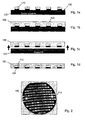
Figures 1a to 1d illustrate an exemplary process for obtaining a wafer-scale chip package. As shown infigure 1a , in a first step individual semiconductor dies (or chips) 110 are placed on acarrier substrate 120, the chips being attached to thecarrier substrate 120 by means of an temporary bonding layer, for example in the form of a double-sideadhesive tape 130. Preferably each die is tested before being placed on thecarrier substrate 120, so that only functioning dies are used. - In a second step, shown in
figure 1b , thedies 110 are moulded into awafer 150 by applying amoulding compound 140 around the dies. The underside of eachdie 110, on which electrical connections are to be made, is protected from themoulding compound 140 by being attached to thecarrier substrate 120. - In a third step, shown in
figure 1c , thewafer 150 is separated from thecarrier substrate 120. Thewafer 150, with electrical connections on the exposedsurfaces 160 of the now embedded dies 110 (figure 1d ), can then be handled as a single unit during subsequent processing steps. A plan view of anexemplary wafer 150, in which a 2-dimensional array ofdies 110 is embedded, is shown infigure 2 . -
Figures 3a and 3b illustrate schematically a subsequent step performed on each wafer, which provides fan-out electrical connection traces from eachdie 110. Electrical connections betweenadjacent dies wafer 150, onesuch connection 320 being shown infigure 3b . Eachconnection 320 connects a diepad 330 of one die 310a to that of another die 310b. Theseconnections 320 are also shown in cross-section infigure 4a , which illustrates thewafer 150 now attached to acarrier substrate 420 with the exposed surfaces on thedies 310 face-up to allow theconnections 320 to be applied. Thewafer 150 is then separated from thecarrier substrate 420 after the connections are applied (figure 4b ). -
Figures 5a to 5d illustrate further processing stages involved in creating a 3-dimensional stack of wafers. Shown infigure 5a , aglue layer 510 is applied to a face of eachwafer 150. Afirst wafer 150a is attached to a carrier substrate 520 (figure 5b ). Asecond wafer 150b is then attached to thefirst wafer 150a with the glue layer 510 (figure 5c ). The process is repeated (figure 5d ) until sufficient layers have been assembled. A 3-dimensional stack 530 is then formed in which eachlayer material 140 andglue layers 510. - As shown in
figure 6 , the 3-dimensional stack 530, in this case comprising four wafer layers, is then divided intoindividual stacks 630a-d in a machining operation. The machining operation preferably comprises a series of sawing operations, for example using a computer-controlled grinding disc to accurately saw through the wafers between adjacent dies. This machining operation exposeselectrical connections 650 on side faces of each of thestacks 630a-d. Theindividual stacks 630a-d can then be removed from thecarrier substrate 520. -
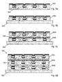
figures 7a to 7c illustrate schematically a subsequent series of processing steps to form electrical connections between each layer of theindividual stacks 630. Thestacks 630 are first subjected to an electroless metal plating process, which deposits ametallic layer 710 over at least oneside face 640 of thestack 630. This process may be performed while thestacks 630a-d are on thecarrier substrate 520, so that electrical output connections on thelower face 650 of each stack are protected. - A particular preferred material for use as the deposited
metal layer 710 is a nickel and gold composition (Ni-Au). Various processes for electroless metal deposition are known in the art, and need not be described here in detail. Further information regarding an exemplary electroless Ni plating process suitable for use with the invention is disclosed by W. Riedel in "Electroless Nickel Plating", ASM International, 1991. - After electroless plating, portions of the
metallic layer 710 are selectively removed from theside face 640 of thestack 630 by means of a sawing operation (figure 7b ). Arotating grinding disc 720 may be used to machinenarrow grooves 730 along theside face 640 of the stack, forming a plurality ofconductive tracks 740 along the side face. The remaining metallic layer, now in the form of conductive tracks extending between an upper surface and thelower surface 650 of thestack 630, connects with the electrical connections 320 (figure 4a ) provided on each layer of the stack, so that a connection can be made from thelower face 650 of thestack 630 to each of the individual dies in the stack (figure 7c ). - A positioning precision of around 7µm is currently possible for the selective sawing step, allowing conductive tracks with a pitch of the order of 25 µm to be produced. The selective sawing process results in several advantages over other techniques such as laser patterning. Firstly, the same equipment can be used that may already be in place for dividing the packages from a stack of wafers, therefore requiring only minor reconfigurations in the process line. Secondly, fine machining by sawing is a well known and mature processing technique, and can achieve high levels of accuracy with low set-up costs as compared with laser machining. Thirdly, sawing can result in a finer scale pitch, and with less resulting surface and sub-surface damage, than laser machining.
- The finished form of a
stack 630 is shown schematically infigure 8 , as attached to a printed circuit board (PCB) by aball grid array 810. Thelower face 650 of thestack 630 provides the electrical connections to the PCB via aball grid array 810. Aredistribution layer 820 on thelower face 630 of the stack, allows for appropriate connections on the lower surface to be made to one or more of the side faces 640, on which are provided theconductive tracks 740 resulting from the preceding stages. With appropriate configuration of connections, each layer of thestack 630, which may be provided with different fan-out connections to connect with different conductive tracks along one or more side faces of the stack, can be addressed through the connections provided on thelower face 650. - Other embodiments are intentionally within the scope of the invention as defined by the appended claims.
Claims (7)
- A method of forming electrical connections on an integrated circuit package, the method comprising:providing a cuboid-shaped stack within which are moulded a plurality of integrated circuit dies, the stack having a lower face with a plurality of electrical connections provided thereon;electroless metal plating the stack to deposit a metallic layer on a side face of the stack; andselectively removing a portion of the metallic layer on the side face of the stack to form a plurality of conductive tracks along the side face, the conductive tracks electrically connecting each of the integrated circuit dies to a selection of the electrical connections on the lower face of the stack,wherein the step of selectively removing a portion of the metallic layer comprises sawing a plurality of grooves along the side face of the stack, the grooves extending between an upper face and the lower face of the stack.
- The method of claim 1 comprising the preceding steps of:providing a plurality of wafers, each wafer comprising a planar array of integrated circuit dies;applying electrical connection traces to a first face of each wafer;stacking the plurality of wafers to form a 3 dimensional array of integrated circuit dies; anddividing the array into a plurality of said cuboid-shaped stacks by cutting the stack of wafers between adjacent integrated circuit dies.
- The method of claim 1 wherein the metallic layer comprises nickel and gold.
- The method of claim 1 wherein the step of electroless metal plating is carried out prior to removal of the stack from a carrier substrate on which a plurality of said stacks are mounted.
- An integrated circuit package comprising a cuboid-shaped stack within which are moulded a plurality of integrated circuit dies, the stack having a lower face with a plurality of electrical connections provided thereon, a plurality of tracks being provided along a side face of the stack to connect the plurality of electrical connections with each of the plurality of integrated circuit dies, each track separated from adjacent tracks by a groove extending between an upper face and the lower face of the stack.
- The integrated circuit package of claim 5 wherein the plurality of tracks are formed of an electroless deposited metal layer.
- The integrated circuit package of claim 6 wherein the metal layer comprises nickel and gold.
Priority Applications (1)
| Application Number | Priority Date | Filing Date | Title |
|---|---|---|---|
| EP20080291240 EP2207200A1 (en) | 2008-12-24 | 2008-12-24 | Stack of molded integrated circuit dies with side surface contact tracks |
Applications Claiming Priority (1)
| Application Number | Priority Date | Filing Date | Title |
|---|---|---|---|
| EP20080291240 EP2207200A1 (en) | 2008-12-24 | 2008-12-24 | Stack of molded integrated circuit dies with side surface contact tracks |
Publications (1)
| Publication Number | Publication Date |
|---|---|
| EP2207200A1 true EP2207200A1 (en) | 2010-07-14 |
Family
ID=40677758
Family Applications (1)
| Application Number | Title | Priority Date | Filing Date |
|---|---|---|---|
| EP20080291240 Ceased EP2207200A1 (en) | 2008-12-24 | 2008-12-24 | Stack of molded integrated circuit dies with side surface contact tracks |
Country Status (1)
| Country | Link |
|---|---|
| EP (1) | EP2207200A1 (en) |
Cited By (1)
| Publication number | Priority date | Publication date | Assignee | Title |
|---|---|---|---|---|
| US10607955B2 (en) | 2017-06-20 | 2020-03-31 | Sandisk Semiconductor (Shanghai) Co. Ltd. | Heterogeneous fan-out structures for memory devices |
Citations (6)
| Publication number | Priority date | Publication date | Assignee | Title |
|---|---|---|---|---|
| US5547906A (en) * | 1992-09-14 | 1996-08-20 | Badehi; Pierre | Methods for producing integrated circuit devices |
| WO2001045172A1 (en) * | 1999-12-15 | 2001-06-21 | 3D Plus | Method and device for interconnecting electronic components in three dimensions |
| US20030047353A1 (en) * | 2001-09-07 | 2003-03-13 | Yamaguchi James Satsuo | Multilayer modules with flexible substrates |
| US20060055039A1 (en) * | 2002-02-07 | 2006-03-16 | Floyd Eide | Stackable layer containing ball grid array package |
| FR2895568A1 (en) * | 2005-12-23 | 2007-06-29 | 3D Plus Sa Sa | COLLECTIVE MANUFACTURING METHOD OF 3D ELECTRONIC MODULES |
| US20070158805A1 (en) * | 2002-04-22 | 2007-07-12 | Gann Keith | BGA-scale stacks comprised of layers containing integrated circuit die and a method for making the same |
-
2008
- 2008-12-24 EP EP20080291240 patent/EP2207200A1/en not_active Ceased
Patent Citations (6)
| Publication number | Priority date | Publication date | Assignee | Title |
|---|---|---|---|---|
| US5547906A (en) * | 1992-09-14 | 1996-08-20 | Badehi; Pierre | Methods for producing integrated circuit devices |
| WO2001045172A1 (en) * | 1999-12-15 | 2001-06-21 | 3D Plus | Method and device for interconnecting electronic components in three dimensions |
| US20030047353A1 (en) * | 2001-09-07 | 2003-03-13 | Yamaguchi James Satsuo | Multilayer modules with flexible substrates |
| US20060055039A1 (en) * | 2002-02-07 | 2006-03-16 | Floyd Eide | Stackable layer containing ball grid array package |
| US20070158805A1 (en) * | 2002-04-22 | 2007-07-12 | Gann Keith | BGA-scale stacks comprised of layers containing integrated circuit die and a method for making the same |
| FR2895568A1 (en) * | 2005-12-23 | 2007-06-29 | 3D Plus Sa Sa | COLLECTIVE MANUFACTURING METHOD OF 3D ELECTRONIC MODULES |
Cited By (1)
| Publication number | Priority date | Publication date | Assignee | Title |
|---|---|---|---|---|
| US10607955B2 (en) | 2017-06-20 | 2020-03-31 | Sandisk Semiconductor (Shanghai) Co. Ltd. | Heterogeneous fan-out structures for memory devices |
Similar Documents
| Publication | Publication Date | Title |
|---|---|---|
| US9761565B2 (en) | Microelectronic packages having embedded sidewall substrates and methods for the producing thereof | |
| US9257415B2 (en) | Stacked microelectronic packages having sidewall conductors and methods for the fabrication thereof | |
| US6818998B2 (en) | Stacked chip package having upper chip provided with trenches and method of manufacturing the same | |
| US7344917B2 (en) | Method for packaging a semiconductor device | |
| US8058098B2 (en) | Method and apparatus for fabricating a plurality of semiconductor devices | |
| US9378967B2 (en) | Method of making a stacked microelectronic package | |
| US7727875B2 (en) | Grooving bumped wafer pre-underfill system | |
| US9299670B2 (en) | Stacked microelectronic packages having sidewall conductors and methods for the fabrication thereof | |
| US7145228B2 (en) | Microelectronic devices | |
| US7511379B1 (en) | Surface mountable direct chip attach device and method including integral integrated circuit | |
| US8617987B2 (en) | Through hole via filling using electroless plating | |
| US5946555A (en) | Wafer level decal for minimal packaging of chips | |
| US20180342434A1 (en) | Method of manufacturing semiconductor devices and corresponding semiconductor device | |
| US20100052164A1 (en) | Wafer level package and method of manufacturing the same | |
| US8093102B2 (en) | Process of forming an electronic device including a plurality of singulated die | |
| US20020180017A1 (en) | Wafer level package having a side package | |
| EP0843357B1 (en) | Method of manufacturing a grid array semiconductor package | |
| JP2004342861A (en) | Chip type electronic component, dummy wafer, methods of manufacturing them, and packaging structure of electronic component | |
| CN101271853A (en) | Method of manufacturing electronic device, substrate and semiconductor device | |
| KR20110107989A (en) | Method for forming stacked semiconductor package | |
| US20100075462A1 (en) | Method of forming semiconductor package | |
| US20080305306A1 (en) | Semiconductor molded panel having reduced warpage | |
| EP2207200A1 (en) | Stack of molded integrated circuit dies with side surface contact tracks | |
| KR101060120B1 (en) | Chip scale semiconductor package and manufacturing method thereof | |
| CN114373688A (en) | Three-dimensional fan-out type wafer level packaging method and packaging structure |
Legal Events
| Date | Code | Title | Description |
|---|---|---|---|
| PUAI | Public reference made under article 153(3) epc to a published international application that has entered the european phase |
Free format text: ORIGINAL CODE: 0009012 |
|
| AK | Designated contracting states |
Kind code of ref document: A1 Designated state(s): AT BE BG CH CY CZ DE DK EE ES FI FR GB GR HR HU IE IS IT LI LT LU LV MC MT NL NO PL PT RO SE SI SK TR |
|
| AX | Request for extension of the european patent |
Extension state: AL BA MK RS |
|
| STAA | Information on the status of an ep patent application or granted ep patent |
Free format text: STATUS: THE APPLICATION HAS BEEN REFUSED |
|
| 18R | Application refused |
Effective date: 20100827 |