EP2157659A1 - Multiband monopole slot antenna - Google Patents
Multiband monopole slot antenna Download PDFInfo
- Publication number
- EP2157659A1 EP2157659A1 EP08170263A EP08170263A EP2157659A1 EP 2157659 A1 EP2157659 A1 EP 2157659A1 EP 08170263 A EP08170263 A EP 08170263A EP 08170263 A EP08170263 A EP 08170263A EP 2157659 A1 EP2157659 A1 EP 2157659A1
- Authority
- EP
- European Patent Office
- Prior art keywords
- monopole slot
- antenna
- monopole
- multiband
- metal surface
- Prior art date
- Legal status (The legal status is an assumption and is not a legal conclusion. Google has not performed a legal analysis and makes no representation as to the accuracy of the status listed.)
- Granted
Links
- 230000005404 monopole Effects 0.000 title claims abstract description 89
- 239000002184 metal Substances 0.000 claims abstract description 30
- 239000000758 substrate Substances 0.000 claims abstract description 28
- 238000005452 bending Methods 0.000 claims description 4
- 238000010295 mobile communication Methods 0.000 description 10
- 230000005855 radiation Effects 0.000 description 6
- 238000005259 measurement Methods 0.000 description 2
- 238000012986 modification Methods 0.000 description 2
- 230000004048 modification Effects 0.000 description 2
- 230000005540 biological transmission Effects 0.000 description 1
- 238000004891 communication Methods 0.000 description 1
- 230000007812 deficiency Effects 0.000 description 1
- 238000011161 development Methods 0.000 description 1
- 238000005516 engineering process Methods 0.000 description 1
- 238000005530 etching Methods 0.000 description 1
- 238000000034 method Methods 0.000 description 1
- 238000007639 printing Methods 0.000 description 1
Images

Classifications
-
- H—ELECTRICITY
- H01—ELECTRIC ELEMENTS
- H01Q—ANTENNAS, i.e. RADIO AERIALS
- H01Q1/00—Details of, or arrangements associated with, antennas
- H01Q1/12—Supports; Mounting means
- H01Q1/22—Supports; Mounting means by structural association with other equipment or articles
- H01Q1/24—Supports; Mounting means by structural association with other equipment or articles with receiving set
- H01Q1/241—Supports; Mounting means by structural association with other equipment or articles with receiving set used in mobile communications, e.g. GSM
- H01Q1/242—Supports; Mounting means by structural association with other equipment or articles with receiving set used in mobile communications, e.g. GSM specially adapted for hand-held use
- H01Q1/243—Supports; Mounting means by structural association with other equipment or articles with receiving set used in mobile communications, e.g. GSM specially adapted for hand-held use with built-in antennas
-
- H—ELECTRICITY
- H01—ELECTRIC ELEMENTS
- H01Q—ANTENNAS, i.e. RADIO AERIALS
- H01Q13/00—Waveguide horns or mouths; Slot antennas; Leaky-waveguide antennas; Equivalent structures causing radiation along the transmission path of a guided wave
- H01Q13/10—Resonant slot antennas
- H01Q13/106—Microstrip slot antennas
-
- H—ELECTRICITY
- H01—ELECTRIC ELEMENTS
- H01Q—ANTENNAS, i.e. RADIO AERIALS
- H01Q21/00—Antenna arrays or systems
- H01Q21/30—Combinations of separate antenna units operating in different wavebands and connected to a common feeder system
-
- H—ELECTRICITY
- H01—ELECTRIC ELEMENTS
- H01Q—ANTENNAS, i.e. RADIO AERIALS
- H01Q5/00—Arrangements for simultaneous operation of antennas on two or more different wavebands, e.g. dual-band or multi-band arrangements
- H01Q5/40—Imbricated or interleaved structures; Combined or electromagnetically coupled arrangements, e.g. comprising two or more non-connected fed radiating elements
Definitions
- the present invention relates to a slot antenna, and more particularly, to a multiband monopole slot antenna suitable for application in mobile communication devices.
- Taiwan patent No. 1293215 entitled “Dual-Band Inverted-F Antenna”
- a ground plane built in the backplane of the LCD display of a notebook computer and a dual-band antenna designed thereon are disclosed.
- the antenna is only suitable for WLAN operation due to its size; it is difficult to fit into a mobile communication device when it is applied as a multiband antenna used in the mobile communication system.
- the antenna disclosed in the present invention comprises: a ground plane, a dielectric substrate, a radiating portion and a microstrip feedline.
- the dielectric substrate is connected to an edge of the ground plane and extends toward the opposite direction of the ground plane.
- the dielectric substrate has a metal surface, which can be formed on the dielectric substrate by printing or etching and the metal surface is electrically connected to the ground plane via at least one electrical connecting point.
- the radiating portion is on the metal surface of the dielectric substrate and comprises at least a first monopole slot, a second monopole slot, and a third monopole slot, wherein the first, the second, and the third monopole slots each have an open end and a terminal, the open end is on a side edge of the metal surface, and the terminal is extended inward the metal surface.
- the second monopole slot is substantially parallel to the first monopole slot; the third monopole slot is positioned between the first monopole slot and the second monopole slot.
- the microstrip feedline is on the surface opposite to the metal surface of the dielectric substrate and can be printed or etched on the dielectric substrate.
- a first end of the microstrip feedline is connected to a signal source, and a second end of the microstrip feedline is an open end.
- the microstrip feedline passes over the first, second, and third monopole slots.
- a section of the microstrip feedline which passes over the third monopole slot is substantially parallel to the third monopole slot, and the microstrip feedline is generally of a step shape.
- the antenna disclosed in the present invention is designed as a multiband monopole slot antenna, which can be operated in communication bands such as GSM850 (824 ⁇ 894 MHz), GSM900 (890 - 960 MHz), and DCS/PCS/UMTS (1710 - 1880 MHz/1850 ⁇ 1990 MHz/1920 ⁇ 2170 MHz).
- the multiband monopole slot antenna is series-fed by the microstrip feedline in different positions of the three monopole slots, wherein the microstrip feedline is generally of a step shape and comprises a section parallel to one of the three monopole slots for controlling the feeding position of the monopole slots so as to generate a resonant mode in the lower-frequency band, thereby enabling multiband operation covering the GSM850/900 and DCS/PCS/UMTS bands.
- the first monopole slot can generate a resonant mode near a quarter wavelength of a lower frequency at about 900 MHz
- the second monopole slot can generate a resonant mode near a quarter wavelength of a higher frequency at about 1900 MHz
- the third monopole slot can also generate a resonant mode near a quarter wavelength of the lower frequency at about 900 MHz to form a lower-frequency band with the resonant mode generated by the first monopole slot; in addition, the resonant mode generated by the second monopole slot can form a higher-frequency band.
- the central frequencies of the lower-frequency band and the higher-frequency band can be adjusted by changing the feeding positions of the microstrip feedline corresponding to the first and the second monopole slots. Furthermore, a section of the microstrip feedline parallel to the third monopole slot can also effectively adjust the resonant mode of the third monopole slot to provide good impedance matching; therefore, the present invention can enable multiband operation covering the GSM850/900 and DCS/PCS/UMTS bands.
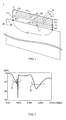
- FIG. 1 illustrates a structural view of a multiband antenna in a first embodiment of the present invention.
- the multiband antenna 1 comprises a ground plane 10, a dielectric substrate 11, a radiating portion 12, and a microstrip feedline 16.
- the ground plane 10 is a metal backplane of an LCD display of a notebook computer.
- the dielectric substrate 11 is at an edge 101 of the ground plane and extends toward the opposite direction of the ground plane 10.
- the dielectric substrate 11 also comprises a metal surface 111, which is electrically connected to the ground plane 10 via at least one electrical connecting point 113.
- the radiating portion 12 on the metal surface 111 of the dielectric substrate 11 comprises at least a first monopole slot 13, a second monopole slot 14, and a third monopole slot 15.
- the first monopole slot 13 comprises an open end 131 and a terminal 132.
- the open end 131 is on a side edge 112 of the metal surface 111, and the terminal 132 extends inward the metal surface 111.
- the second monopole slot 14 is substantially parallel to the first monopole slot 13 and comprises an open end 141 and a terminal 142.
- the open end 141 is on the side edge 112 of the metal surface 111, and the terminal 142 extends inward the metal surface 111.
- the third monopole slot 15 is positioned between the first monopole slot 13 and the second monopole slot 14 and comprises an open end 151 and a terminal 152.
- the open end 151 is on the side edge 112 of the metal surface 111, and the terminal 152 extends inward the metal surface 111.
- the microstrip feedline 16 is generally of a step shape and is on the surface opposite to the metal surface 111 of the dielectric substrate 11. A first end of the microstrip feedline 16 is connected to a signal source 17, and a second end of the microstrip feedline 16 is an open end 161. The microstrip feedline 16 passes over the first monopole slot 13, the second monopole slot 14, and third monopole slot 15. A section 162 of the microstrip feedline 16 which passes over the third monopole slot 15 is substantially parallel to the third monopole slot 15.
- the ground plane 10 being a metal backplane of an LCD display of a notebook computer, is designed to have a length of 260 mm and a width of 200 mm;
- the first monopole slot 13 of the radiating portion 12 has a length of 55 mm (about a quarter wavelength at 900 MHz);
- the second monopole slot 14 has a length of 30 mm (about a quarter wavelength at 1900 MHz);
- the third monopole slot 15 has a length of 58 mm (about a quarter wavelength at 900 MHz).
- the radiating portion 12 is printed or etched on the dielectric substrate 11, which is 60 mm long, 10 mm wide, and 0.8 mm thick.
- FIG. 2 shows a measurement of the return loss of the first embodiment of the present invention.
- the first monopole slot 13 and the third monopole slot 15 can respectively generate a quarter-wavelength resonant mode to jointly form a lower-frequency band 21 of the multiband antenna 1, and the second monopole slot 14 can generate a quarter-wavelength resonant mode to form a higher-frequency band 22.
- the operating bandwidth of the lower-frequency band is about 200 MHz (785 - 985 MHz), which covers the GSM850 (824 - 894 MHz) and the GSM900 (890 ⁇ 960 MHz) bands;
- the operating bandwidth of the higher-frequency band is about 670 MHz (1630 - 2300 MHz), which covers the DCS (1710 - 1880 MHz), PCS (1850 - 1990 MHz), and UMTS (1920 ⁇ 2170 MHz) bands.
- FIG. 3 and FIG. 4 respectively show the gain and the radiation efficiency of the first embodiment of the present invention in a lower-frequency band 21 and a higher-frequency band 22.
- the antenna gain 31 in the lower-frequency band 21 ranges from 0.1 dBi to 0.8 dBi, and the radiation efficiency 32 ranges from 55% to 70%;
- the antenna gain 41 in the higher-frequency band 22 ranges from 0.4 dBi to 2.5 dBi, and the radiation efficiency 42 ranges from 82% to 94%. Therefore, the radiation characteristics of the multiband antenna 1 are suitable for application in mobile communication devices.
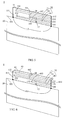
- FIG. 5 illustrates a structural view of the multiband antenna in a second embodiment of the present invention.
- the third monopole slot 55 of the multiband antenna 5 comprises at least two bendings and substantially forms a step shape to keep the terminal 132 of the first monopole slot 13 separated from the terminal 552 of the third monopole slot 55 at a desired distance.
- Other structures of the antenna 5 are the same as those of the antenna 1 of the first embodiment.
- FIG. 6 illustrates a structural view of the multiband antenna in a third embodiment of the present invention.
- the dielectric substrate 61 of the multiband antenna 6 has a bending to allow a portion of the dielectric substrate 61 substantially vertical to the ground plane.
- Other structures of the antenna 6 are the same as those of the antenna 1 of the first embodiment. In this way, the multiband antenna 6 can have various heights and thicknesses to allow placement in different positions in mobile communication devices.
- antennas in the second and the third embodiments can also provide multiband operations as described in the first embodiment.
Abstract
Description
- The present invention relates to a slot antenna, and more particularly, to a multiband monopole slot antenna suitable for application in mobile communication devices.
- The fast development of mobile communication technology and its related market has created various applications for notebook computers, such as the traditional wireless local area network (WLAN) and mobile communications. Among all the factors affecting mobile communication applications, the performance of the antenna is critical to wireless transmission and reception quality. Presently, antennas embedded in notebook computers are mostly used for WLAN operation.
- In the prior art, such as Taiwan patent No.
1293215 - Therefore, it is necessary to provide a multiband antenna with a small size to overcome the deficiency of the techniques of the prior art.
- It is an objective of the present invention to provide an antenna for mobile communication devices, wherein the antenna covers operating bands such as the GSM850/900/DCS/PCS/UMTS bands and provides advantages such as a simple structure and a compact size, and wherein the antenna can easily be printed or etched on a dielectric substrate to fit into mobile communication devices such as notebook computers. In order to achieve the above objectives, the antenna disclosed in the present invention comprises: a ground plane, a dielectric substrate, a radiating portion and a microstrip feedline. The dielectric substrate is connected to an edge of the ground plane and extends toward the opposite direction of the ground plane. The dielectric substrate has a metal surface, which can be formed on the dielectric substrate by printing or etching and the metal surface is electrically connected to the ground plane via at least one electrical connecting point. The radiating portion is on the metal surface of the dielectric substrate and comprises at least a first monopole slot, a second monopole slot, and a third monopole slot, wherein the first, the second, and the third monopole slots each have an open end and a terminal, the open end is on a side edge of the metal surface, and the terminal is extended inward the metal surface. Furthermore, the second monopole slot is substantially parallel to the first monopole slot; the third monopole slot is positioned between the first monopole slot and the second monopole slot. The microstrip feedline is on the surface opposite to the metal surface of the dielectric substrate and can be printed or etched on the dielectric substrate. A first end of the microstrip feedline is connected to a signal source, and a second end of the microstrip feedline is an open end. The microstrip feedline passes over the first, second, and third monopole slots. A section of the microstrip feedline which passes over the third monopole slot is substantially parallel to the third monopole slot, and the microstrip feedline is generally of a step shape.
- The antenna disclosed in the present invention is designed as a multiband monopole slot antenna, which can be operated in communication bands such as GSM850 (824 ∼ 894 MHz), GSM900 (890 - 960 MHz), and DCS/PCS/UMTS (1710 - 1880 MHz/1850 ∼ 1990 MHz/1920 ∼ 2170 MHz). The multiband monopole slot antenna is series-fed by the microstrip feedline in different positions of the three monopole slots, wherein the microstrip feedline is generally of a step shape and comprises a section parallel to one of the three monopole slots for controlling the feeding position of the monopole slots so as to generate a resonant mode in the lower-frequency band, thereby enabling multiband operation covering the GSM850/900 and DCS/PCS/UMTS bands.
- In one embodiment of the present invention, the first monopole slot can generate a resonant mode near a quarter wavelength of a lower frequency at about 900 MHz, the second monopole slot can generate a resonant mode near a quarter wavelength of a higher frequency at about 1900 MHz, and the third monopole slot can also generate a resonant mode near a quarter wavelength of the lower frequency at about 900 MHz to form a lower-frequency band with the resonant mode generated by the first monopole slot; in addition, the resonant mode generated by the second monopole slot can form a higher-frequency band. The central frequencies of the lower-frequency band and the higher-frequency band can be adjusted by changing the feeding positions of the microstrip feedline corresponding to the first and the second monopole slots. Furthermore, a section of the microstrip feedline parallel to the third monopole slot can also effectively adjust the resonant mode of the third monopole slot to provide good impedance matching; therefore, the present invention can enable multiband operation covering the GSM850/900 and DCS/PCS/UMTS bands.
-
-
FIG 1 illustrates a structural view of a multiband antenna in a first embodiment of the present invention; -
FIG. 2 shows a measurement of the return loss of the first embodiment of the present invention; -
FIG. 3 shows a gain and a radiation efficiency of the first embodiment of the present invention in the lower-frequency band; -
FIG. 4 shows a gain and a radiation efficiency of the first embodiment of the present invention in the higher-frequency band; -
FIG. 5 illustrates a structural view of the multiband antenna in a second embodiment of the present invention; and -
FIG. 6 illustrates a structural view of the multiband antenna in a third embodiment of the present invention. - The advantages and innovative features of the invention will become more apparent from the following detailed description when taken in conjunction with the accompanying drawings.
-
FIG. 1 illustrates a structural view of a multiband antenna in a first embodiment of the present invention. Themultiband antenna 1 comprises aground plane 10, adielectric substrate 11, a radiatingportion 12, and amicrostrip feedline 16. In this embodiment, theground plane 10 is a metal backplane of an LCD display of a notebook computer. - The
dielectric substrate 11 is at anedge 101 of the ground plane and extends toward the opposite direction of theground plane 10. Thedielectric substrate 11 also comprises ametal surface 111, which is electrically connected to theground plane 10 via at least oneelectrical connecting point 113. - The
radiating portion 12 on themetal surface 111 of thedielectric substrate 11 comprises at least afirst monopole slot 13, asecond monopole slot 14, and athird monopole slot 15. - The
first monopole slot 13 comprises anopen end 131 and aterminal 132. Theopen end 131 is on aside edge 112 of themetal surface 111, and theterminal 132 extends inward themetal surface 111. - The
second monopole slot 14 is substantially parallel to thefirst monopole slot 13 and comprises anopen end 141 and aterminal 142. Theopen end 141 is on theside edge 112 of themetal surface 111, and theterminal 142 extends inward themetal surface 111. - The
third monopole slot 15 is positioned between thefirst monopole slot 13 and thesecond monopole slot 14 and comprises anopen end 151 and aterminal 152. Theopen end 151 is on theside edge 112 of themetal surface 111, and theterminal 152 extends inward themetal surface 111. - The
microstrip feedline 16 is generally of a step shape and is on the surface opposite to themetal surface 111 of thedielectric substrate 11. A first end of themicrostrip feedline 16 is connected to asignal source 17, and a second end of themicrostrip feedline 16 is anopen end 161. Themicrostrip feedline 16 passes over thefirst monopole slot 13, thesecond monopole slot 14, andthird monopole slot 15. Asection 162 of themicrostrip feedline 16 which passes over thethird monopole slot 15 is substantially parallel to thethird monopole slot 15. - In this embodiment, the
ground plane 10, being a metal backplane of an LCD display of a notebook computer, is designed to have a length of 260 mm and a width of 200 mm; thefirst monopole slot 13 of theradiating portion 12 has a length of 55 mm (about a quarter wavelength at 900 MHz); thesecond monopole slot 14 has a length of 30 mm (about a quarter wavelength at 1900 MHz); thethird monopole slot 15 has a length of 58 mm (about a quarter wavelength at 900 MHz). Furthermore, theradiating portion 12 is printed or etched on thedielectric substrate 11, which is 60 mm long, 10 mm wide, and 0.8 mm thick. - Please refer to
FIG. 2 , which shows a measurement of the return loss of the first embodiment of the present invention. Thefirst monopole slot 13 and thethird monopole slot 15 can respectively generate a quarter-wavelength resonant mode to jointly form a lower-frequency band 21 of themultiband antenna 1, and thesecond monopole slot 14 can generate a quarter-wavelength resonant mode to form a higher-frequency band 22. From the experimental results, under the definition of 6-dB return loss, the operating bandwidth of the lower-frequency band is about 200 MHz (785 - 985 MHz), which covers the GSM850 (824 - 894 MHz) and the GSM900 (890 ∼ 960 MHz) bands; the operating bandwidth of the higher-frequency band is about 670 MHz (1630 - 2300 MHz), which covers the DCS (1710 - 1880 MHz), PCS (1850 - 1990 MHz), and UMTS (1920 ∼ 2170 MHz) bands. -
FIG. 3 and FIG. 4 respectively show the gain and the radiation efficiency of the first embodiment of the present invention in a lower-frequency band 21 and a higher-frequency band 22. From the figures, the antenna gain 31 in the lower-frequency band 21 ranges from 0.1 dBi to 0.8 dBi, and theradiation efficiency 32 ranges from 55% to 70%; the antenna gain 41 in the higher-frequency band 22 ranges from 0.4 dBi to 2.5 dBi, and theradiation efficiency 42 ranges from 82% to 94%. Therefore, the radiation characteristics of themultiband antenna 1 are suitable for application in mobile communication devices. -
FIG. 5 illustrates a structural view of the multiband antenna in a second embodiment of the present invention. In this embodiment, thethird monopole slot 55 of themultiband antenna 5 comprises at least two bendings and substantially forms a step shape to keep theterminal 132 of thefirst monopole slot 13 separated from theterminal 552 of thethird monopole slot 55 at a desired distance. Other structures of theantenna 5 are the same as those of theantenna 1 of the first embodiment. - Now please refer to
FIG. 6 , which illustrates a structural view of the multiband antenna in a third embodiment of the present invention. In this embodiment, thedielectric substrate 61 of themultiband antenna 6 has a bending to allow a portion of thedielectric substrate 61 substantially vertical to the ground plane. Other structures of theantenna 6 are the same as those of theantenna 1 of the first embodiment. In this way, themultiband antenna 6 can have various heights and thicknesses to allow placement in different positions in mobile communication devices. - It is noted that the antennas in the second and the third embodiments can also provide multiband operations as described in the first embodiment.
- It is noted that the above-mentioned embodiments are only for illustration, it is intended that the present invention cover modifications and variations of this invention provided they fall within the scope of the following claims and their equivalents. Therefore, it will be apparent to those skilled in the art that various modifications and variations can be made to the structure of the present invention without departing from the scope or spirit of the invention.
Claims (11)
- A multiband monopole slot antenna comprising:a ground plane;a dielectric substrate connected to an edge of the ground plane and extending toward the opposite direction of the ground plane, the dielectric substrate having a metal surface electrically connected to the ground plane via at least one electrical connecting point;a radiating portion on the metal surface of the dielectric substrate comprising:a first monopole slot having a first open end and a first terminal, wherein the first open end is disposed on a side edge of the metal surface, and the first terminal is extended inward the metal surface;a second monopole slot substantially parallel to the first monopole slot, the second monopole slot having a second open end and a second terminal, wherein the second open end is disposed on a side edge of the metal surface, and the second terminal is extended inward the metal surface; anda third monopole slot disposed between the first monopole slot and the second monopole slot, the third monopole slot having a third open end and a third terminal, wherein the third open end is disposed on a side edge of the metal surface, and the third terminal is extended inward the metal surface; anda microstrip feedline formed generally of a step shape, wherein the microstrip feedline is on the surface opposite to the metal surface of the dielectric substrate; a first end of the microstrip feedline is connected to a signal source, and a second end of the microstrip feedline is an open end; and the microstrip feedline passes over the first, second and third monopole slots; a section of the microstrip feedline which passes over the third monopole slot is substantially parallel to the third monopole slot.
- The multiband monopole slot antenna as claimed in claim 1, wherein the ground plane is a metal backplane of an LCD display of a notebook computer.
- The multiband monopole slot antenna as claimed in claim 1, wherein the metal surface is printed or etched on the dielectric substrate.
- The multiband monopole slot antenna as claimed in claim 1, wherein the microstrip feedline is printed or etched on the dielectric substrate.
- The multiband monopole slot antenna as claimed in claim 1, wherein the length of the first monopole slot is substantially a quarter wavelength of a central frequency of a lower-frequency band of the antenna.
- The multiband monopole slot antenna as claimed in claim 1, wherein the length of the second monopole slot is substantially a quarter wavelength of a central frequency of a higher-frequency band of the antenna.
- The multiband monopole slot antenna as claimed in claim 1, wherein the length of the third monopole slot is substantially a quarter wavelength of a central frequency of a lower-frequency band of the antenna.
- The multiband monopole slot antenna as claimed in claim 1, wherein the third monopole slot comprises at least two bendings.
- The multiband monopole slot antenna as claimed in claim 1, wherein the dielectric substrate has a bending to allow a portion of the dielectric substrate substantially vertical to the ground plane.
- The multiband monopole slot antenna as claimed in claim 1, wherein the first monopole slot and the third monopole slot are used for generating a lower-frequency resonant mode; and the second monopole slot is used for generating a higher-frequency resonant mode.
- The multiband monopole slot antenna as claimed in claim 1, wherein the length of the first monopole slot is substantially a quarter wavelength of a central frequency of a first lower-frequency band of the antenna, the length of the second monopole slot is substantially a quarter wavelength of a central frequency of a higher-frequency band of the antenna, and the length of the third monopole slot is substantially a quarter wavelength of a central frequency of a second lower-frequency band of the antenna, wherein the central frequency of the first lower-frequency band is different from the central frequency of the second lower-frequency band.
Applications Claiming Priority (1)
| Application Number | Priority Date | Filing Date | Title |
|---|---|---|---|
| TW097131769A TWI341053B (en) | 2008-08-20 | 2008-08-20 | Multiband monopole slot antenna |
Publications (2)
| Publication Number | Publication Date |
|---|---|
| EP2157659A1 true EP2157659A1 (en) | 2010-02-24 |
| EP2157659B1 EP2157659B1 (en) | 2011-01-12 |
Family
ID=40474966
Family Applications (1)
| Application Number | Title | Priority Date | Filing Date |
|---|---|---|---|
| EP08170263A Active EP2157659B1 (en) | 2008-08-20 | 2008-11-28 | Multiband monopole slot antenna |
Country Status (5)
| Country | Link |
|---|---|
| US (1) | US8223083B2 (en) |
| EP (1) | EP2157659B1 (en) |
| AT (1) | ATE495559T1 (en) |
| DE (1) | DE602008004522D1 (en) |
| TW (1) | TWI341053B (en) |
Cited By (4)
| Publication number | Priority date | Publication date | Assignee | Title |
|---|---|---|---|---|
| CN101800361A (en) * | 2010-03-23 | 2010-08-11 | 中兴通讯股份有限公司 | Wireless device |
| EP2445053A1 (en) * | 2010-10-22 | 2012-04-25 | Acer Incorporated | Mobile communication device and antenna |
| EP2509158A3 (en) * | 2011-04-08 | 2013-04-03 | Acer Incorporated | Communication electronic device and antenna structure thereof |
| CN104241865A (en) * | 2013-06-11 | 2014-12-24 | 深圳富泰宏精密工业有限公司 | Antenna assembly |
Families Citing this family (13)
| Publication number | Priority date | Publication date | Assignee | Title |
|---|---|---|---|---|
| TWI436526B (en) * | 2010-04-20 | 2014-05-01 | Quanta Comp Inc | Can suppress the maximum gain of the multi-frequency antenna |
| WO2012047085A1 (en) * | 2010-10-05 | 2012-04-12 | Laird Technologies, Inc. | Multi-band, wide-band antennas |
| CN102456943B (en) * | 2010-10-28 | 2014-12-17 | 宏碁股份有限公司 | Mobile communication device and antenna device |
| CN102842747B (en) * | 2011-06-21 | 2014-12-17 | 英华达(上海)科技有限公司 | Single-pole slot antenna structure with adjustable slot |
| TWI619308B (en) * | 2013-06-10 | 2018-03-21 | 群邁通訊股份有限公司 | Antenna assembly |
| KR20140148150A (en) * | 2013-06-21 | 2014-12-31 | 삼성전자주식회사 | Antenna device and display apparatus having the same |
| CN104319477B (en) * | 2014-09-18 | 2018-02-27 | 联想(北京)有限公司 | A kind of antenna and electronic equipment |
| WO2016042516A1 (en) | 2014-09-18 | 2016-03-24 | Arad Measuring Technologies Ltd. | Utility meter having a meter register utilizing a multiple resonance antenna |
| US10128579B2 (en) | 2015-02-13 | 2018-11-13 | Commscope Technologies Llc | Dipole antenna element with open-end traces |
| TWI689134B (en) * | 2016-05-10 | 2020-03-21 | 和碩聯合科技股份有限公司 | Dual band printed antenna |
| TWI635653B (en) | 2017-04-18 | 2018-09-11 | 華碩電腦股份有限公司 | Antenna element |
| TWI641185B (en) | 2017-06-27 | 2018-11-11 | 華碩電腦股份有限公司 | Communication device and antenna assembly thereof |
| CN111952724B (en) * | 2020-09-28 | 2022-11-08 | 西安电子科技大学 | Antenna module and electronic equipment |
Citations (6)
| Publication number | Priority date | Publication date | Assignee | Title |
|---|---|---|---|---|
| GB2325349A (en) * | 1997-05-09 | 1998-11-18 | Motorola Inc | Multi-band slot antenna |
| US6404394B1 (en) * | 1999-12-23 | 2002-06-11 | Tyco Electronics Logistics Ag | Dual polarization slot antenna assembly |
| US20040056812A1 (en) * | 2000-01-12 | 2004-03-25 | Emag Technologies, Inc. | Multifunction antenna |
| US20050200545A1 (en) * | 2004-03-12 | 2005-09-15 | Centurion Wireless Technologies | Dual slot radiator single feedpoint printed circuit board antenna |
| EP1670093A1 (en) * | 2004-12-07 | 2006-06-14 | Sony Ericsson Mobile Communications AB | Antenna arrangement |
| TWI293215B (en) | 2006-06-13 | 2008-02-01 | Yageo Corp | Dual-band inverted-f antenna |
Family Cites Families (5)
| Publication number | Priority date | Publication date | Assignee | Title |
|---|---|---|---|---|
| US2942263A (en) * | 1957-02-25 | 1960-06-21 | Gen Dynamics Corp | Antennas |
| US5640386A (en) | 1995-06-06 | 1997-06-17 | Globalstar L.P. | Two-system protocol conversion transceiver repeater |
| SE516322C2 (en) * | 1999-12-01 | 2001-12-17 | Fci Katrineholm Ab | Angled connector and method of mounting one |
| KR100531218B1 (en) * | 2003-08-27 | 2006-01-10 | 한국전자통신연구원 | Slot antenna having slots formed on both sides of dielectric substrate |
| US8373610B2 (en) * | 2007-12-18 | 2013-02-12 | Apple Inc. | Microslot antennas for electronic devices |
-
2008
- 2008-08-20 TW TW097131769A patent/TWI341053B/en active
- 2008-11-13 US US12/269,924 patent/US8223083B2/en active Active
- 2008-11-28 DE DE602008004522T patent/DE602008004522D1/en active Active
- 2008-11-28 AT AT08170263T patent/ATE495559T1/en not_active IP Right Cessation
- 2008-11-28 EP EP08170263A patent/EP2157659B1/en active Active
Patent Citations (6)
| Publication number | Priority date | Publication date | Assignee | Title |
|---|---|---|---|---|
| GB2325349A (en) * | 1997-05-09 | 1998-11-18 | Motorola Inc | Multi-band slot antenna |
| US6404394B1 (en) * | 1999-12-23 | 2002-06-11 | Tyco Electronics Logistics Ag | Dual polarization slot antenna assembly |
| US20040056812A1 (en) * | 2000-01-12 | 2004-03-25 | Emag Technologies, Inc. | Multifunction antenna |
| US20050200545A1 (en) * | 2004-03-12 | 2005-09-15 | Centurion Wireless Technologies | Dual slot radiator single feedpoint printed circuit board antenna |
| EP1670093A1 (en) * | 2004-12-07 | 2006-06-14 | Sony Ericsson Mobile Communications AB | Antenna arrangement |
| TWI293215B (en) | 2006-06-13 | 2008-02-01 | Yageo Corp | Dual-band inverted-f antenna |
Cited By (8)
| Publication number | Priority date | Publication date | Assignee | Title |
|---|---|---|---|---|
| CN101800361A (en) * | 2010-03-23 | 2010-08-11 | 中兴通讯股份有限公司 | Wireless device |
| WO2011116575A1 (en) * | 2010-03-23 | 2011-09-29 | 中兴通讯股份有限公司 | Wireless device |
| EP2445053A1 (en) * | 2010-10-22 | 2012-04-25 | Acer Incorporated | Mobile communication device and antenna |
| US8599084B2 (en) | 2010-10-22 | 2013-12-03 | Acer Incorporated | Mobile communication device and antenna |
| EP2509158A3 (en) * | 2011-04-08 | 2013-04-03 | Acer Incorporated | Communication electronic device and antenna structure thereof |
| US9035841B2 (en) | 2011-04-08 | 2015-05-19 | Acer Incorporated | Communication electronic device and antenna structure thereof |
| CN104241865A (en) * | 2013-06-11 | 2014-12-24 | 深圳富泰宏精密工业有限公司 | Antenna assembly |
| CN104241865B (en) * | 2013-06-11 | 2018-10-30 | 深圳富泰宏精密工业有限公司 | Antenna module |
Also Published As
| Publication number | Publication date |
|---|---|
| TW201010182A (en) | 2010-03-01 |
| EP2157659B1 (en) | 2011-01-12 |
| US8223083B2 (en) | 2012-07-17 |
| ATE495559T1 (en) | 2011-01-15 |
| TWI341053B (en) | 2011-04-21 |
| US20100045556A1 (en) | 2010-02-25 |
| DE602008004522D1 (en) | 2011-02-24 |
Similar Documents
| Publication | Publication Date | Title |
|---|---|---|
| EP2157659B1 (en) | Multiband monopole slot antenna | |
| EP2117073B1 (en) | A coupled-fed multiband loop antenna | |
| US7626551B2 (en) | Multi-band planar inverted-F antenna | |
| US7333067B2 (en) | Multi-band antenna with wide bandwidth | |
| US8698673B2 (en) | Multiband antenna | |
| US6509882B2 (en) | Low SAR broadband antenna assembly | |
| US8373604B2 (en) | Multiband mobile communication device and antenna thereof | |
| EP2065972B1 (en) | Dual-band-antenna | |
| EP2509158B1 (en) | Communication electronic device and antenna structure thereof | |
| US20100060528A1 (en) | Dual-frequency antenna | |
| US8599086B2 (en) | Monopole slot antenna | |
| US20050195119A1 (en) | Integrated multiband antennas for computing devices | |
| EP2610967B1 (en) | Communication device and antenna structure therein | |
| US8587486B2 (en) | Multi-band antenna | |
| EP2381529B1 (en) | Communications structures including antennas with separate antenna branches coupled to feed and ground conductors | |
| US20110102272A1 (en) | Mobile Communication Device and Antenna Thereof | |
| US20120162022A1 (en) | Multi-band antenna | |
| EP2202845B1 (en) | Multi-band antenna | |
| EP2584647A2 (en) | Communication device and antenna structure thereof | |
| US7391375B1 (en) | Multi-band antenna | |
| TWI448006B (en) | Antenna with multi-bands | |
| US7791545B2 (en) | Multiband antenna | |
| JP5060938B2 (en) | Wireless LAN antenna and wireless communication device | |
| US20120162023A1 (en) | Multi-band antenna | |
| US20090033565A1 (en) | Antenna structure and wireless communication apparatus thereof |
Legal Events
| Date | Code | Title | Description |
|---|---|---|---|
| PUAI | Public reference made under article 153(3) epc to a published international application that has entered the european phase |
Free format text: ORIGINAL CODE: 0009012 |
|
| 17P | Request for examination filed |
Effective date: 20090812 |
|
| AK | Designated contracting states |
Kind code of ref document: A1 Designated state(s): AT BE BG CH CY CZ DE DK EE ES FI FR GB GR HR HU IE IS IT LI LT LU LV MC MT NL NO PL PT RO SE SI SK TR |
|
| AX | Request for extension of the european patent |
Extension state: AL BA MK RS |
|
| GRAP | Despatch of communication of intention to grant a patent |
Free format text: ORIGINAL CODE: EPIDOSNIGR1 |
|
| GRAS | Grant fee paid |
Free format text: ORIGINAL CODE: EPIDOSNIGR3 |
|
| AKX | Designation fees paid |
Designated state(s): AT BE BG CH CY CZ DE DK EE ES FI FR GB GR HR HU IE IS IT LI LT LU LV MC MT NL NO PL PT RO SE SI SK TR |
|
| RAP1 | Party data changed (applicant data changed or rights of an application transferred) |
Owner name: ACER INC. |
|
| GRAA | (expected) grant |
Free format text: ORIGINAL CODE: 0009210 |
|
| AK | Designated contracting states |
Kind code of ref document: B1 Designated state(s): AT BE BG CH CY CZ DE DK EE ES FI FR GB GR HR HU IE IS IT LI LT LU LV MC MT NL NO PL PT RO SE SI SK TR |
|
| REG | Reference to a national code |
Ref country code: GB Ref legal event code: FG4D |
|
| REG | Reference to a national code |
Ref country code: CH Ref legal event code: EP |
|
| REG | Reference to a national code |
Ref country code: IE Ref legal event code: FG4D |
|
| REF | Corresponds to: |
Ref document number: 602008004522 Country of ref document: DE Date of ref document: 20110224 Kind code of ref document: P |
|
| REG | Reference to a national code |
Ref country code: DE Ref legal event code: R096 Ref document number: 602008004522 Country of ref document: DE Effective date: 20110224 |
|
| REG | Reference to a national code |
Ref country code: NL Ref legal event code: T3 |
|
| LTIE | Lt: invalidation of european patent or patent extension |
Effective date: 20110112 |
|
| PG25 | Lapsed in a contracting state [announced via postgrant information from national office to epo] |
Ref country code: HR Free format text: LAPSE BECAUSE OF FAILURE TO SUBMIT A TRANSLATION OF THE DESCRIPTION OR TO PAY THE FEE WITHIN THE PRESCRIBED TIME-LIMIT Effective date: 20110112 Ref country code: SE Free format text: LAPSE BECAUSE OF FAILURE TO SUBMIT A TRANSLATION OF THE DESCRIPTION OR TO PAY THE FEE WITHIN THE PRESCRIBED TIME-LIMIT Effective date: 20110112 Ref country code: GR Free format text: LAPSE BECAUSE OF FAILURE TO SUBMIT A TRANSLATION OF THE DESCRIPTION OR TO PAY THE FEE WITHIN THE PRESCRIBED TIME-LIMIT Effective date: 20110413 Ref country code: ES Free format text: LAPSE BECAUSE OF FAILURE TO SUBMIT A TRANSLATION OF THE DESCRIPTION OR TO PAY THE FEE WITHIN THE PRESCRIBED TIME-LIMIT Effective date: 20110423 Ref country code: PT Free format text: LAPSE BECAUSE OF FAILURE TO SUBMIT A TRANSLATION OF THE DESCRIPTION OR TO PAY THE FEE WITHIN THE PRESCRIBED TIME-LIMIT Effective date: 20110512 Ref country code: NO Free format text: LAPSE BECAUSE OF FAILURE TO SUBMIT A TRANSLATION OF THE DESCRIPTION OR TO PAY THE FEE WITHIN THE PRESCRIBED TIME-LIMIT Effective date: 20110412 Ref country code: IS Free format text: LAPSE BECAUSE OF FAILURE TO SUBMIT A TRANSLATION OF THE DESCRIPTION OR TO PAY THE FEE WITHIN THE PRESCRIBED TIME-LIMIT Effective date: 20110512 Ref country code: LV Free format text: LAPSE BECAUSE OF FAILURE TO SUBMIT A TRANSLATION OF THE DESCRIPTION OR TO PAY THE FEE WITHIN THE PRESCRIBED TIME-LIMIT Effective date: 20110112 Ref country code: LT Free format text: LAPSE BECAUSE OF FAILURE TO SUBMIT A TRANSLATION OF THE DESCRIPTION OR TO PAY THE FEE WITHIN THE PRESCRIBED TIME-LIMIT Effective date: 20110112 |
|
| PG25 | Lapsed in a contracting state [announced via postgrant information from national office to epo] |
Ref country code: SI Free format text: LAPSE BECAUSE OF FAILURE TO SUBMIT A TRANSLATION OF THE DESCRIPTION OR TO PAY THE FEE WITHIN THE PRESCRIBED TIME-LIMIT Effective date: 20110112 Ref country code: PL Free format text: LAPSE BECAUSE OF FAILURE TO SUBMIT A TRANSLATION OF THE DESCRIPTION OR TO PAY THE FEE WITHIN THE PRESCRIBED TIME-LIMIT Effective date: 20110112 Ref country code: BE Free format text: LAPSE BECAUSE OF FAILURE TO SUBMIT A TRANSLATION OF THE DESCRIPTION OR TO PAY THE FEE WITHIN THE PRESCRIBED TIME-LIMIT Effective date: 20110112 Ref country code: BG Free format text: LAPSE BECAUSE OF FAILURE TO SUBMIT A TRANSLATION OF THE DESCRIPTION OR TO PAY THE FEE WITHIN THE PRESCRIBED TIME-LIMIT Effective date: 20110412 Ref country code: CY Free format text: LAPSE BECAUSE OF FAILURE TO SUBMIT A TRANSLATION OF THE DESCRIPTION OR TO PAY THE FEE WITHIN THE PRESCRIBED TIME-LIMIT Effective date: 20110112 Ref country code: AT Free format text: LAPSE BECAUSE OF FAILURE TO SUBMIT A TRANSLATION OF THE DESCRIPTION OR TO PAY THE FEE WITHIN THE PRESCRIBED TIME-LIMIT Effective date: 20110112 |
|
| PG25 | Lapsed in a contracting state [announced via postgrant information from national office to epo] |
Ref country code: EE Free format text: LAPSE BECAUSE OF FAILURE TO SUBMIT A TRANSLATION OF THE DESCRIPTION OR TO PAY THE FEE WITHIN THE PRESCRIBED TIME-LIMIT Effective date: 20110112 Ref country code: DK Free format text: LAPSE BECAUSE OF FAILURE TO SUBMIT A TRANSLATION OF THE DESCRIPTION OR TO PAY THE FEE WITHIN THE PRESCRIBED TIME-LIMIT Effective date: 20110112 |
|
| PLBE | No opposition filed within time limit |
Free format text: ORIGINAL CODE: 0009261 |
|
| STAA | Information on the status of an ep patent application or granted ep patent |
Free format text: STATUS: NO OPPOSITION FILED WITHIN TIME LIMIT |
|
| PG25 | Lapsed in a contracting state [announced via postgrant information from national office to epo] |
Ref country code: CZ Free format text: LAPSE BECAUSE OF FAILURE TO SUBMIT A TRANSLATION OF THE DESCRIPTION OR TO PAY THE FEE WITHIN THE PRESCRIBED TIME-LIMIT Effective date: 20110112 Ref country code: RO Free format text: LAPSE BECAUSE OF FAILURE TO SUBMIT A TRANSLATION OF THE DESCRIPTION OR TO PAY THE FEE WITHIN THE PRESCRIBED TIME-LIMIT Effective date: 20110112 Ref country code: SK Free format text: LAPSE BECAUSE OF FAILURE TO SUBMIT A TRANSLATION OF THE DESCRIPTION OR TO PAY THE FEE WITHIN THE PRESCRIBED TIME-LIMIT Effective date: 20110112 |
|
| 26N | No opposition filed |
Effective date: 20111013 |
|
| REG | Reference to a national code |
Ref country code: DE Ref legal event code: R097 Ref document number: 602008004522 Country of ref document: DE Effective date: 20111013 |
|
| PG25 | Lapsed in a contracting state [announced via postgrant information from national office to epo] |
Ref country code: MC Free format text: LAPSE BECAUSE OF NON-PAYMENT OF DUE FEES Effective date: 20111130 |
|
| REG | Reference to a national code |
Ref country code: IE Ref legal event code: MM4A |
|
| PG25 | Lapsed in a contracting state [announced via postgrant information from national office to epo] |
Ref country code: IE Free format text: LAPSE BECAUSE OF NON-PAYMENT OF DUE FEES Effective date: 20111128 |
|
| PG25 | Lapsed in a contracting state [announced via postgrant information from national office to epo] |
Ref country code: MT Free format text: LAPSE BECAUSE OF FAILURE TO SUBMIT A TRANSLATION OF THE DESCRIPTION OR TO PAY THE FEE WITHIN THE PRESCRIBED TIME-LIMIT Effective date: 20110112 |
|
| PG25 | Lapsed in a contracting state [announced via postgrant information from national office to epo] |
Ref country code: LU Free format text: LAPSE BECAUSE OF NON-PAYMENT OF DUE FEES Effective date: 20111128 |
|
| REG | Reference to a national code |
Ref country code: CH Ref legal event code: PL |
|
| PG25 | Lapsed in a contracting state [announced via postgrant information from national office to epo] |
Ref country code: LI Free format text: LAPSE BECAUSE OF NON-PAYMENT OF DUE FEES Effective date: 20121130 Ref country code: CH Free format text: LAPSE BECAUSE OF NON-PAYMENT OF DUE FEES Effective date: 20121130 |
|
| PG25 | Lapsed in a contracting state [announced via postgrant information from national office to epo] |
Ref country code: TR Free format text: LAPSE BECAUSE OF FAILURE TO SUBMIT A TRANSLATION OF THE DESCRIPTION OR TO PAY THE FEE WITHIN THE PRESCRIBED TIME-LIMIT Effective date: 20110112 |
|
| PG25 | Lapsed in a contracting state [announced via postgrant information from national office to epo] |
Ref country code: HU Free format text: LAPSE BECAUSE OF FAILURE TO SUBMIT A TRANSLATION OF THE DESCRIPTION OR TO PAY THE FEE WITHIN THE PRESCRIBED TIME-LIMIT Effective date: 20110112 |
|
| REG | Reference to a national code |
Ref country code: FR Ref legal event code: PLFP Year of fee payment: 8 |
|
| REG | Reference to a national code |
Ref country code: FR Ref legal event code: PLFP Year of fee payment: 9 |
|
| REG | Reference to a national code |
Ref country code: FR Ref legal event code: PLFP Year of fee payment: 10 |
|
| REG | Reference to a national code |
Ref country code: FR Ref legal event code: PLFP Year of fee payment: 11 |
|
| PGFP | Annual fee paid to national office [announced via postgrant information from national office to epo] |
Ref country code: NL Payment date: 20231013 Year of fee payment: 16 |
|
| PGFP | Annual fee paid to national office [announced via postgrant information from national office to epo] |
Ref country code: GB Payment date: 20231006 Year of fee payment: 16 |
|
| PGFP | Annual fee paid to national office [announced via postgrant information from national office to epo] |
Ref country code: IT Payment date: 20231010 Year of fee payment: 16 Ref country code: FR Payment date: 20231009 Year of fee payment: 16 Ref country code: FI Payment date: 20231116 Year of fee payment: 16 Ref country code: DE Payment date: 20231010 Year of fee payment: 16 |