EP2105960A2 - Improved adhesion to copper and copper electromigration resistance - Google Patents
Improved adhesion to copper and copper electromigration resistance Download PDFInfo
- Publication number
- EP2105960A2 EP2105960A2 EP09155899A EP09155899A EP2105960A2 EP 2105960 A2 EP2105960 A2 EP 2105960A2 EP 09155899 A EP09155899 A EP 09155899A EP 09155899 A EP09155899 A EP 09155899A EP 2105960 A2 EP2105960 A2 EP 2105960A2
- Authority
- EP
- European Patent Office
- Prior art keywords
- layer
- copper
- plasma
- treatment
- adhesion
- Prior art date
- Legal status (The legal status is an assumption and is not a legal conclusion. Google has not performed a legal analysis and makes no representation as to the accuracy of the status listed.)
- Granted
Links
- 239000010949 copper Substances 0.000 title abstract description 108
- RYGMFSIKBFXOCR-UHFFFAOYSA-N Copper Chemical compound [Cu] RYGMFSIKBFXOCR-UHFFFAOYSA-N 0.000 title abstract description 105
- 229910052802 copper Inorganic materials 0.000 title abstract description 105
- 229910052751 metal Inorganic materials 0.000 claims abstract description 38
- 239000002184 metal Substances 0.000 claims abstract description 38
- 239000002243 precursor Substances 0.000 claims abstract description 36
- 230000004888 barrier function Effects 0.000 claims abstract description 31
- 125000002524 organometallic group Chemical group 0.000 claims abstract description 29
- 238000004519 manufacturing process Methods 0.000 claims abstract description 5
- VXKWYPOMXBVZSJ-UHFFFAOYSA-N tetramethyltin Chemical group C[Sn](C)(C)C VXKWYPOMXBVZSJ-UHFFFAOYSA-N 0.000 claims description 70
- 238000011282 treatment Methods 0.000 claims description 58
- 238000000034 method Methods 0.000 claims description 52
- 229910052581 Si3N4 Inorganic materials 0.000 claims description 50
- 239000011135 tin Substances 0.000 claims description 37
- 229910052718 tin Inorganic materials 0.000 claims description 36
- 239000000203 mixture Substances 0.000 claims description 33
- ATJFFYVFTNAWJD-UHFFFAOYSA-N Tin Chemical group [Sn] ATJFFYVFTNAWJD-UHFFFAOYSA-N 0.000 claims description 30
- XUIMIQQOPSSXEZ-UHFFFAOYSA-N Silicon Chemical compound [Si] XUIMIQQOPSSXEZ-UHFFFAOYSA-N 0.000 claims description 23
- 229910052710 silicon Inorganic materials 0.000 claims description 23
- 239000010703 silicon Substances 0.000 claims description 23
- 238000000151 deposition Methods 0.000 claims description 21
- PXHVJJICTQNCMI-UHFFFAOYSA-N nickel Substances [Ni] PXHVJJICTQNCMI-UHFFFAOYSA-N 0.000 claims description 20
- 238000002203 pretreatment Methods 0.000 claims description 20
- 239000002904 solvent Substances 0.000 claims description 20
- 239000000758 substrate Substances 0.000 claims description 15
- KXCAEQNNTZANTK-UHFFFAOYSA-N stannane Chemical compound [SnH4] KXCAEQNNTZANTK-UHFFFAOYSA-N 0.000 claims description 12
- 229910000083 tin tetrahydride Inorganic materials 0.000 claims description 12
- VYPSYNLAJGMNEJ-UHFFFAOYSA-N Silicium dioxide Chemical compound O=[Si]=O VYPSYNLAJGMNEJ-UHFFFAOYSA-N 0.000 claims description 11
- 238000012545 processing Methods 0.000 claims description 11
- QVGXLLKOCUKJST-UHFFFAOYSA-N atomic oxygen Chemical compound [O] QVGXLLKOCUKJST-UHFFFAOYSA-N 0.000 claims description 9
- AEVRNKXPLOTCBW-UHFFFAOYSA-N carbon monoxide;cobalt;cyclopenta-1,3-diene Chemical compound [Co].[O+]#[C-].[O+]#[C-].C=1C=C[CH-]C=1 AEVRNKXPLOTCBW-UHFFFAOYSA-N 0.000 claims description 9
- 239000001301 oxygen Substances 0.000 claims description 9
- 229910052760 oxygen Inorganic materials 0.000 claims description 9
- HCHKCACWOHOZIP-UHFFFAOYSA-N Zinc Chemical compound [Zn] HCHKCACWOHOZIP-UHFFFAOYSA-N 0.000 claims description 8
- 229910017052 cobalt Inorganic materials 0.000 claims description 8
- 239000010941 cobalt Substances 0.000 claims description 8
- GUTLYIVDDKVIGB-UHFFFAOYSA-N cobalt atom Chemical compound [Co] GUTLYIVDDKVIGB-UHFFFAOYSA-N 0.000 claims description 8
- 239000012530 fluid Substances 0.000 claims description 8
- 239000011701 zinc Substances 0.000 claims description 8
- 229910052725 zinc Inorganic materials 0.000 claims description 8
- VYZAMTAEIAYCRO-UHFFFAOYSA-N Chromium Chemical compound [Cr] VYZAMTAEIAYCRO-UHFFFAOYSA-N 0.000 claims description 7
- 229910052804 chromium Inorganic materials 0.000 claims description 7
- 239000011651 chromium Substances 0.000 claims description 7
- HQVNEWCFYHHQES-UHFFFAOYSA-N silicon nitride Chemical compound N12[Si]34N5[Si]62N3[Si]51N64 HQVNEWCFYHHQES-UHFFFAOYSA-N 0.000 claims description 7
- VWHXTCKWIVCDGV-UHFFFAOYSA-N C(C)C1(C=CC=C1)[Ni]C1(C=CC=C1)CC Chemical compound C(C)C1(C=CC=C1)[Ni]C1(C=CC=C1)CC VWHXTCKWIVCDGV-UHFFFAOYSA-N 0.000 claims description 6
- DEIHRWXJCZMTHF-UHFFFAOYSA-N [Mn].[CH]1C=CC=C1 Chemical compound [Mn].[CH]1C=CC=C1 DEIHRWXJCZMTHF-UHFFFAOYSA-N 0.000 claims description 6
- 150000004678 hydrides Chemical class 0.000 claims description 6
- 229910052759 nickel Inorganic materials 0.000 claims description 6
- NFHFRUOZVGFOOS-UHFFFAOYSA-N palladium;triphenylphosphane Chemical compound [Pd].C1=CC=CC=C1P(C=1C=CC=CC=1)C1=CC=CC=C1.C1=CC=CC=C1P(C=1C=CC=CC=1)C1=CC=CC=C1.C1=CC=CC=C1P(C=1C=CC=CC=1)C1=CC=CC=C1.C1=CC=CC=C1P(C=1C=CC=CC=1)C1=CC=CC=C1 NFHFRUOZVGFOOS-UHFFFAOYSA-N 0.000 claims description 6
- KXCAEQNNTZANTK-NJJOSUKLSA-N tetradeuteriostannane Chemical compound [Sn]([2H])([2H])([2H])[2H] KXCAEQNNTZANTK-NJJOSUKLSA-N 0.000 claims description 6
- DBGVGMSCBYYSLD-UHFFFAOYSA-N tributylstannane Chemical compound CCCC[SnH](CCCC)CCCC DBGVGMSCBYYSLD-UHFFFAOYSA-N 0.000 claims description 6
- NXHILIPIEUBEPD-UHFFFAOYSA-H tungsten hexafluoride Chemical compound F[W](F)(F)(F)(F)F NXHILIPIEUBEPD-UHFFFAOYSA-H 0.000 claims description 6
- 229910052814 silicon oxide Inorganic materials 0.000 claims description 5
- 125000004122 cyclic group Chemical group 0.000 claims description 4
- 239000007789 gas Substances 0.000 claims description 4
- 229930195733 hydrocarbon Natural products 0.000 claims description 4
- 150000002430 hydrocarbons Chemical class 0.000 claims description 4
- 239000004065 semiconductor Substances 0.000 claims description 4
- HJAHIISBZWIGFO-UHFFFAOYSA-N CN(C)C.CC[Zn]CC Chemical compound CN(C)C.CC[Zn]CC HJAHIISBZWIGFO-UHFFFAOYSA-N 0.000 claims description 3
- 239000004215 Carbon black (E152) Substances 0.000 claims description 3
- 229910019813 Cr(CO)6 Inorganic materials 0.000 claims description 3
- HAPVSOMXSKSUFV-UHFFFAOYSA-N N(=O)[Co] Chemical compound N(=O)[Co] HAPVSOMXSKSUFV-UHFFFAOYSA-N 0.000 claims description 3
- 229910008940 W(CO)6 Inorganic materials 0.000 claims description 3
- 229910000086 alane Inorganic materials 0.000 claims description 3
- AZDRQVAHHNSJOQ-UHFFFAOYSA-N alumane Chemical compound [AlH3] AZDRQVAHHNSJOQ-UHFFFAOYSA-N 0.000 claims description 3
- 150000001412 amines Chemical class 0.000 claims description 3
- FQNHWXHRAUXLFU-UHFFFAOYSA-N carbon monoxide;tungsten Chemical group [W].[O+]#[C-].[O+]#[C-].[O+]#[C-].[O+]#[C-].[O+]#[C-].[O+]#[C-] FQNHWXHRAUXLFU-UHFFFAOYSA-N 0.000 claims description 3
- HQWPLXHWEZZGKY-UHFFFAOYSA-N diethylzinc Chemical compound CC[Zn]CC HQWPLXHWEZZGKY-UHFFFAOYSA-N 0.000 claims description 3
- AXAZMDOAUQTMOW-UHFFFAOYSA-N dimethylzinc Chemical compound C[Zn]C AXAZMDOAUQTMOW-UHFFFAOYSA-N 0.000 claims description 3
- DAZXVJBJRMWXJP-UHFFFAOYSA-N n,n-dimethylethylamine Chemical compound CCN(C)C DAZXVJBJRMWXJP-UHFFFAOYSA-N 0.000 claims description 3
- HBMJWWWQQXIZIP-UHFFFAOYSA-N silicon carbide Chemical compound [Si+]#[C-] HBMJWWWQQXIZIP-UHFFFAOYSA-N 0.000 claims description 3
- 229910010271 silicon carbide Inorganic materials 0.000 claims description 3
- JLTRXTDYQLMHGR-UHFFFAOYSA-N trimethylaluminium Chemical compound C[Al](C)C JLTRXTDYQLMHGR-UHFFFAOYSA-N 0.000 claims description 3
- IPSRAFUHLHIWAR-UHFFFAOYSA-N zinc;ethane Chemical compound [Zn+2].[CH2-]C.[CH2-]C IPSRAFUHLHIWAR-UHFFFAOYSA-N 0.000 claims description 3
- KJTLSVCANCCWHF-UHFFFAOYSA-N Ruthenium Chemical compound [Ru] KJTLSVCANCCWHF-UHFFFAOYSA-N 0.000 claims description 2
- RTAQQCXQSZGOHL-UHFFFAOYSA-N Titanium Chemical compound [Ti] RTAQQCXQSZGOHL-UHFFFAOYSA-N 0.000 claims description 2
- NRTOMJZYCJJWKI-UHFFFAOYSA-N Titanium nitride Chemical compound [Ti]#N NRTOMJZYCJJWKI-UHFFFAOYSA-N 0.000 claims description 2
- 238000004891 communication Methods 0.000 claims description 2
- 229910052707 ruthenium Inorganic materials 0.000 claims description 2
- 229910052715 tantalum Inorganic materials 0.000 claims description 2
- GUVRBAGPIYLISA-UHFFFAOYSA-N tantalum atom Chemical group [Ta] GUVRBAGPIYLISA-UHFFFAOYSA-N 0.000 claims description 2
- MZLGASXMSKOWSE-UHFFFAOYSA-N tantalum nitride Chemical compound [Ta]#N MZLGASXMSKOWSE-UHFFFAOYSA-N 0.000 claims description 2
- 239000010936 titanium Substances 0.000 claims description 2
- 229910052719 titanium Inorganic materials 0.000 claims description 2
- 238000011144 upstream manufacturing Methods 0.000 claims description 2
- 210000002381 plasma Anatomy 0.000 description 87
- 239000010410 layer Substances 0.000 description 86
- 239000001257 hydrogen Substances 0.000 description 23
- 229910052739 hydrogen Inorganic materials 0.000 description 23
- 238000000623 plasma-assisted chemical vapour deposition Methods 0.000 description 20
- 230000008569 process Effects 0.000 description 20
- 238000001004 secondary ion mass spectrometry Methods 0.000 description 20
- BLRPTPMANUNPDV-UHFFFAOYSA-N Silane Chemical compound [SiH4] BLRPTPMANUNPDV-UHFFFAOYSA-N 0.000 description 18
- 230000008021 deposition Effects 0.000 description 18
- 239000000463 material Substances 0.000 description 18
- VLKZOEOYAKHREP-UHFFFAOYSA-N n-Hexane Chemical compound CCCCCC VLKZOEOYAKHREP-UHFFFAOYSA-N 0.000 description 18
- QGZKDVFQNNGYKY-UHFFFAOYSA-N Ammonia Chemical compound N QGZKDVFQNNGYKY-UHFFFAOYSA-N 0.000 description 16
- 239000011521 glass Substances 0.000 description 16
- 238000005259 measurement Methods 0.000 description 16
- UFHFLCQGNIYNRP-UHFFFAOYSA-N Hydrogen Chemical compound [H][H] UFHFLCQGNIYNRP-UHFFFAOYSA-N 0.000 description 15
- 229910000069 nitrogen hydride Inorganic materials 0.000 description 13
- IJGRMHOSHXDMSA-UHFFFAOYSA-N Atomic nitrogen Chemical compound N#N IJGRMHOSHXDMSA-UHFFFAOYSA-N 0.000 description 12
- 238000004833 X-ray photoelectron spectroscopy Methods 0.000 description 12
- 239000000523 sample Substances 0.000 description 11
- QPLDLSVMHZLSFG-UHFFFAOYSA-N Copper oxide Chemical compound [Cu]=O QPLDLSVMHZLSFG-UHFFFAOYSA-N 0.000 description 10
- 238000009832 plasma treatment Methods 0.000 description 10
- 235000012431 wafers Nutrition 0.000 description 10
- 238000004458 analytical method Methods 0.000 description 9
- 230000032798 delamination Effects 0.000 description 9
- 239000003989 dielectric material Substances 0.000 description 9
- 230000000694 effects Effects 0.000 description 9
- 239000005751 Copper oxide Substances 0.000 description 8
- 229910052799 carbon Inorganic materials 0.000 description 8
- 238000005229 chemical vapour deposition Methods 0.000 description 8
- 229910000431 copper oxide Inorganic materials 0.000 description 8
- 150000002431 hydrogen Chemical class 0.000 description 8
- 230000008859 change Effects 0.000 description 7
- 229910000077 silane Inorganic materials 0.000 description 7
- OKTJSMMVPCPJKN-UHFFFAOYSA-N Carbon Chemical compound [C] OKTJSMMVPCPJKN-UHFFFAOYSA-N 0.000 description 6
- 230000015556 catabolic process Effects 0.000 description 6
- 239000001307 helium Substances 0.000 description 6
- 229910052734 helium Inorganic materials 0.000 description 6
- SWQJXJOGLNCZEY-UHFFFAOYSA-N helium atom Chemical compound [He] SWQJXJOGLNCZEY-UHFFFAOYSA-N 0.000 description 6
- 229910052757 nitrogen Inorganic materials 0.000 description 6
- -1 dibutyldimethyltin Chemical compound 0.000 description 5
- LFQSCWFLJHTTHZ-UHFFFAOYSA-N Ethanol Chemical compound CCO LFQSCWFLJHTTHZ-UHFFFAOYSA-N 0.000 description 4
- 229910052782 aluminium Inorganic materials 0.000 description 4
- XAGFODPZIPBFFR-UHFFFAOYSA-N aluminium Chemical compound [Al] XAGFODPZIPBFFR-UHFFFAOYSA-N 0.000 description 4
- 238000000231 atomic layer deposition Methods 0.000 description 4
- 230000015572 biosynthetic process Effects 0.000 description 4
- 238000005137 deposition process Methods 0.000 description 4
- 238000009792 diffusion process Methods 0.000 description 4
- 229910000881 Cu alloy Inorganic materials 0.000 description 3
- RTZKZFJDLAIYFH-UHFFFAOYSA-N Diethyl ether Chemical compound CCOCC RTZKZFJDLAIYFH-UHFFFAOYSA-N 0.000 description 3
- 239000004593 Epoxy Substances 0.000 description 3
- PWHULOQIROXLJO-UHFFFAOYSA-N Manganese Chemical compound [Mn] PWHULOQIROXLJO-UHFFFAOYSA-N 0.000 description 3
- OKKJLVBELUTLKV-UHFFFAOYSA-N Methanol Chemical compound OC OKKJLVBELUTLKV-UHFFFAOYSA-N 0.000 description 3
- YXFVVABEGXRONW-UHFFFAOYSA-N Toluene Chemical compound CC1=CC=CC=C1 YXFVVABEGXRONW-UHFFFAOYSA-N 0.000 description 3
- 239000000853 adhesive Substances 0.000 description 3
- 230000001070 adhesive effect Effects 0.000 description 3
- 229940104869 fluorosilicate Drugs 0.000 description 3
- 229910052748 manganese Inorganic materials 0.000 description 3
- 239000011572 manganese Substances 0.000 description 3
- 230000009467 reduction Effects 0.000 description 3
- 235000012239 silicon dioxide Nutrition 0.000 description 3
- 239000000377 silicon dioxide Substances 0.000 description 3
- 239000000243 solution Substances 0.000 description 3
- 238000012360 testing method Methods 0.000 description 3
- CSCPPACGZOOCGX-UHFFFAOYSA-N Acetone Chemical compound CC(C)=O CSCPPACGZOOCGX-UHFFFAOYSA-N 0.000 description 2
- XKRFYHLGVUSROY-UHFFFAOYSA-N Argon Chemical compound [Ar] XKRFYHLGVUSROY-UHFFFAOYSA-N 0.000 description 2
- KFZMGEQAYNKOFK-UHFFFAOYSA-N Isopropanol Chemical compound CC(C)O KFZMGEQAYNKOFK-UHFFFAOYSA-N 0.000 description 2
- IMNFDUFMRHMDMM-UHFFFAOYSA-N N-Heptane Chemical compound CCCCCCC IMNFDUFMRHMDMM-UHFFFAOYSA-N 0.000 description 2
- OFBQJSOFQDEBGM-UHFFFAOYSA-N Pentane Chemical compound CCCCC OFBQJSOFQDEBGM-UHFFFAOYSA-N 0.000 description 2
- BQCADISMDOOEFD-UHFFFAOYSA-N Silver Chemical compound [Ag] BQCADISMDOOEFD-UHFFFAOYSA-N 0.000 description 2
- WYURNTSHIVDZCO-UHFFFAOYSA-N Tetrahydrofuran Chemical compound C1CCOC1 WYURNTSHIVDZCO-UHFFFAOYSA-N 0.000 description 2
- 239000002318 adhesion promoter Substances 0.000 description 2
- 238000001505 atmospheric-pressure chemical vapour deposition Methods 0.000 description 2
- 239000012159 carrier gas Substances 0.000 description 2
- 238000006243 chemical reaction Methods 0.000 description 2
- 239000004020 conductor Substances 0.000 description 2
- NBBQQQJUOYRZCA-UHFFFAOYSA-N diethoxymethylsilane Chemical compound CCOC([SiH3])OCC NBBQQQJUOYRZCA-UHFFFAOYSA-N 0.000 description 2
- 150000002148 esters Chemical class 0.000 description 2
- 238000002347 injection Methods 0.000 description 2
- 239000007924 injection Substances 0.000 description 2
- 239000007788 liquid Substances 0.000 description 2
- 238000004518 low pressure chemical vapour deposition Methods 0.000 description 2
- WPBNNNQJVZRUHP-UHFFFAOYSA-L manganese(2+);methyl n-[[2-(methoxycarbonylcarbamothioylamino)phenyl]carbamothioyl]carbamate;n-[2-(sulfidocarbothioylamino)ethyl]carbamodithioate Chemical compound [Mn+2].[S-]C(=S)NCCNC([S-])=S.COC(=O)NC(=S)NC1=CC=CC=C1NC(=S)NC(=O)OC WPBNNNQJVZRUHP-UHFFFAOYSA-L 0.000 description 2
- 239000007769 metal material Substances 0.000 description 2
- 239000003361 porogen Substances 0.000 description 2
- 229910052709 silver Inorganic materials 0.000 description 2
- 239000004332 silver Substances 0.000 description 2
- 239000002356 single layer Substances 0.000 description 2
- YHQGMYUVUMAZJR-UHFFFAOYSA-N α-terpinene Chemical compound CC(C)C1=CC=C(C)CC1 YHQGMYUVUMAZJR-UHFFFAOYSA-N 0.000 description 2
- ZYVYEJXMYBUCMN-UHFFFAOYSA-N 1-methoxy-2-methylpropane Chemical compound COCC(C)C ZYVYEJXMYBUCMN-UHFFFAOYSA-N 0.000 description 1
- XDTMQSROBMDMFD-UHFFFAOYSA-N Cyclohexane Chemical compound C1CCCCC1 XDTMQSROBMDMFD-UHFFFAOYSA-N 0.000 description 1
- WSTYNZDAOAEEKG-UHFFFAOYSA-N Mayol Natural products CC1=C(O)C(=O)C=C2C(CCC3(C4CC(C(CC4(CCC33C)C)=O)C)C)(C)C3=CC=C21 WSTYNZDAOAEEKG-UHFFFAOYSA-N 0.000 description 1
- CTQNGGLPUBDAKN-UHFFFAOYSA-N O-Xylene Chemical compound CC1=CC=CC=C1C CTQNGGLPUBDAKN-UHFFFAOYSA-N 0.000 description 1
- HMDDXIMCDZRSNE-UHFFFAOYSA-N [C].[Si] Chemical compound [C].[Si] HMDDXIMCDZRSNE-UHFFFAOYSA-N 0.000 description 1
- 238000004026 adhesive bonding Methods 0.000 description 1
- 150000001298 alcohols Chemical class 0.000 description 1
- 150000001299 aldehydes Chemical class 0.000 description 1
- 229910021529 ammonia Inorganic materials 0.000 description 1
- 229910052786 argon Inorganic materials 0.000 description 1
- 150000004945 aromatic hydrocarbons Chemical class 0.000 description 1
- QUQFTIVBFKLPCL-UHFFFAOYSA-L copper;2-amino-3-[(2-amino-2-carboxylatoethyl)disulfanyl]propanoate Chemical group [Cu+2].[O-]C(=O)C(N)CSSCC(N)C([O-])=O QUQFTIVBFKLPCL-UHFFFAOYSA-L 0.000 description 1
- 230000008878 coupling Effects 0.000 description 1
- 238000010168 coupling process Methods 0.000 description 1
- 238000005859 coupling reaction Methods 0.000 description 1
- WJTCGQSWYFHTAC-UHFFFAOYSA-N cyclooctane Chemical compound C1CCCCCCC1 WJTCGQSWYFHTAC-UHFFFAOYSA-N 0.000 description 1
- 239000004914 cyclooctane Substances 0.000 description 1
- 230000000593 degrading effect Effects 0.000 description 1
- 238000002716 delivery method Methods 0.000 description 1
- 238000001514 detection method Methods 0.000 description 1
- 238000010790 dilution Methods 0.000 description 1
- 239000012895 dilution Substances 0.000 description 1
- 150000002170 ethers Chemical class 0.000 description 1
- 238000002474 experimental method Methods 0.000 description 1
- AHAREKHAZNPPMI-UHFFFAOYSA-N hexa-1,3-diene Chemical compound CCC=CC=C AHAREKHAZNPPMI-UHFFFAOYSA-N 0.000 description 1
- 230000006872 improvement Effects 0.000 description 1
- 238000011065 in-situ storage Methods 0.000 description 1
- 230000010354 integration Effects 0.000 description 1
- 239000011229 interlayer Substances 0.000 description 1
- 150000002576 ketones Chemical class 0.000 description 1
- 239000012705 liquid precursor Substances 0.000 description 1
- 238000001465 metallisation Methods 0.000 description 1
- 150000002739 metals Chemical class 0.000 description 1
- 238000004377 microelectronic Methods 0.000 description 1
- 238000007254 oxidation reaction Methods 0.000 description 1
- 230000001590 oxidative effect Effects 0.000 description 1
- HFPZCAJZSCWRBC-UHFFFAOYSA-N p-cymene Chemical compound CC(C)C1=CC=C(C)C=C1 HFPZCAJZSCWRBC-UHFFFAOYSA-N 0.000 description 1
- 230000000704 physical effect Effects 0.000 description 1
- 239000011148 porous material Substances 0.000 description 1
- 230000001737 promoting effect Effects 0.000 description 1
- 238000001228 spectrum Methods 0.000 description 1
- 238000004544 sputter deposition Methods 0.000 description 1
- 238000004381 surface treatment Methods 0.000 description 1
- YLQBMQCUIZJEEH-UHFFFAOYSA-N tetrahydrofuran Natural products C=1C=COC=1 YLQBMQCUIZJEEH-UHFFFAOYSA-N 0.000 description 1
- 238000007669 thermal treatment Methods 0.000 description 1
- 231100000331 toxic Toxicity 0.000 description 1
- 230000002588 toxic effect Effects 0.000 description 1
- 230000008016 vaporization Effects 0.000 description 1
- 238000009834 vaporization Methods 0.000 description 1
- 239000008096 xylene Substances 0.000 description 1
Images


Classifications
-
- H—ELECTRICITY
- H01—ELECTRIC ELEMENTS
- H01L—SEMICONDUCTOR DEVICES NOT COVERED BY CLASS H10
- H01L21/00—Processes or apparatus adapted for the manufacture or treatment of semiconductor or solid state devices or of parts thereof
- H01L21/02—Manufacture or treatment of semiconductor devices or of parts thereof
- H01L21/04—Manufacture or treatment of semiconductor devices or of parts thereof the devices having at least one potential-jump barrier or surface barrier, e.g. PN junction, depletion layer or carrier concentration layer
- H01L21/18—Manufacture or treatment of semiconductor devices or of parts thereof the devices having at least one potential-jump barrier or surface barrier, e.g. PN junction, depletion layer or carrier concentration layer the devices having semiconductor bodies comprising elements of Group IV of the Periodic System or AIIIBV compounds with or without impurities, e.g. doping materials
- H01L21/30—Treatment of semiconductor bodies using processes or apparatus not provided for in groups H01L21/20 - H01L21/26
- H01L21/31—Treatment of semiconductor bodies using processes or apparatus not provided for in groups H01L21/20 - H01L21/26 to form insulating layers thereon, e.g. for masking or by using photolithographic techniques; After treatment of these layers; Selection of materials for these layers
-
- H—ELECTRICITY
- H01—ELECTRIC ELEMENTS
- H01L—SEMICONDUCTOR DEVICES NOT COVERED BY CLASS H10
- H01L21/00—Processes or apparatus adapted for the manufacture or treatment of semiconductor or solid state devices or of parts thereof
- H01L21/70—Manufacture or treatment of devices consisting of a plurality of solid state components formed in or on a common substrate or of parts thereof; Manufacture of integrated circuit devices or of parts thereof
- H01L21/71—Manufacture of specific parts of devices defined in group H01L21/70
- H01L21/768—Applying interconnections to be used for carrying current between separate components within a device comprising conductors and dielectrics
- H01L21/76838—Applying interconnections to be used for carrying current between separate components within a device comprising conductors and dielectrics characterised by the formation and the after-treatment of the conductors
- H01L21/76841—Barrier, adhesion or liner layers
- H01L21/76843—Barrier, adhesion or liner layers formed in openings in a dielectric
- H01L21/76849—Barrier, adhesion or liner layers formed in openings in a dielectric the layer being positioned on top of the main fill metal
-
- C—CHEMISTRY; METALLURGY
- C23—COATING METALLIC MATERIAL; COATING MATERIAL WITH METALLIC MATERIAL; CHEMICAL SURFACE TREATMENT; DIFFUSION TREATMENT OF METALLIC MATERIAL; COATING BY VACUUM EVAPORATION, BY SPUTTERING, BY ION IMPLANTATION OR BY CHEMICAL VAPOUR DEPOSITION, IN GENERAL; INHIBITING CORROSION OF METALLIC MATERIAL OR INCRUSTATION IN GENERAL
- C23C—COATING METALLIC MATERIAL; COATING MATERIAL WITH METALLIC MATERIAL; SURFACE TREATMENT OF METALLIC MATERIAL BY DIFFUSION INTO THE SURFACE, BY CHEMICAL CONVERSION OR SUBSTITUTION; COATING BY VACUUM EVAPORATION, BY SPUTTERING, BY ION IMPLANTATION OR BY CHEMICAL VAPOUR DEPOSITION, IN GENERAL
- C23C16/00—Chemical coating by decomposition of gaseous compounds, without leaving reaction products of surface material in the coating, i.e. chemical vapour deposition [CVD] processes
- C23C16/02—Pretreatment of the material to be coated
-
- C—CHEMISTRY; METALLURGY
- C23—COATING METALLIC MATERIAL; COATING MATERIAL WITH METALLIC MATERIAL; CHEMICAL SURFACE TREATMENT; DIFFUSION TREATMENT OF METALLIC MATERIAL; COATING BY VACUUM EVAPORATION, BY SPUTTERING, BY ION IMPLANTATION OR BY CHEMICAL VAPOUR DEPOSITION, IN GENERAL; INHIBITING CORROSION OF METALLIC MATERIAL OR INCRUSTATION IN GENERAL
- C23C—COATING METALLIC MATERIAL; COATING MATERIAL WITH METALLIC MATERIAL; SURFACE TREATMENT OF METALLIC MATERIAL BY DIFFUSION INTO THE SURFACE, BY CHEMICAL CONVERSION OR SUBSTITUTION; COATING BY VACUUM EVAPORATION, BY SPUTTERING, BY ION IMPLANTATION OR BY CHEMICAL VAPOUR DEPOSITION, IN GENERAL
- C23C16/00—Chemical coating by decomposition of gaseous compounds, without leaving reaction products of surface material in the coating, i.e. chemical vapour deposition [CVD] processes
- C23C16/56—After-treatment
-
- H—ELECTRICITY
- H01—ELECTRIC ELEMENTS
- H01L—SEMICONDUCTOR DEVICES NOT COVERED BY CLASS H10
- H01L21/00—Processes or apparatus adapted for the manufacture or treatment of semiconductor or solid state devices or of parts thereof
- H01L21/02—Manufacture or treatment of semiconductor devices or of parts thereof
- H01L21/04—Manufacture or treatment of semiconductor devices or of parts thereof the devices having at least one potential-jump barrier or surface barrier, e.g. PN junction, depletion layer or carrier concentration layer
- H01L21/18—Manufacture or treatment of semiconductor devices or of parts thereof the devices having at least one potential-jump barrier or surface barrier, e.g. PN junction, depletion layer or carrier concentration layer the devices having semiconductor bodies comprising elements of Group IV of the Periodic System or AIIIBV compounds with or without impurities, e.g. doping materials
- H01L21/28—Manufacture of electrodes on semiconductor bodies using processes or apparatus not provided for in groups H01L21/20 - H01L21/268
- H01L21/283—Deposition of conductive or insulating materials for electrodes conducting electric current
- H01L21/285—Deposition of conductive or insulating materials for electrodes conducting electric current from a gas or vapour, e.g. condensation
- H01L21/28506—Deposition of conductive or insulating materials for electrodes conducting electric current from a gas or vapour, e.g. condensation of conductive layers
- H01L21/28512—Deposition of conductive or insulating materials for electrodes conducting electric current from a gas or vapour, e.g. condensation of conductive layers on semiconductor bodies comprising elements of Group IV of the Periodic System
- H01L21/28556—Deposition of conductive or insulating materials for electrodes conducting electric current from a gas or vapour, e.g. condensation of conductive layers on semiconductor bodies comprising elements of Group IV of the Periodic System by chemical means, e.g. CVD, LPCVD, PECVD, laser CVD
-
- H—ELECTRICITY
- H01—ELECTRIC ELEMENTS
- H01L—SEMICONDUCTOR DEVICES NOT COVERED BY CLASS H10
- H01L21/00—Processes or apparatus adapted for the manufacture or treatment of semiconductor or solid state devices or of parts thereof
- H01L21/70—Manufacture or treatment of devices consisting of a plurality of solid state components formed in or on a common substrate or of parts thereof; Manufacture of integrated circuit devices or of parts thereof
- H01L21/71—Manufacture of specific parts of devices defined in group H01L21/70
- H01L21/768—Applying interconnections to be used for carrying current between separate components within a device comprising conductors and dielectrics
- H01L21/76801—Applying interconnections to be used for carrying current between separate components within a device comprising conductors and dielectrics characterised by the formation and the after-treatment of the dielectrics, e.g. smoothing
- H01L21/76829—Applying interconnections to be used for carrying current between separate components within a device comprising conductors and dielectrics characterised by the formation and the after-treatment of the dielectrics, e.g. smoothing characterised by the formation of thin functional dielectric layers, e.g. dielectric etch-stop, barrier, capping or liner layers
- H01L21/76834—Applying interconnections to be used for carrying current between separate components within a device comprising conductors and dielectrics characterised by the formation and the after-treatment of the dielectrics, e.g. smoothing characterised by the formation of thin functional dielectric layers, e.g. dielectric etch-stop, barrier, capping or liner layers formation of thin insulating films on the sidewalls or on top of conductors
-
- H—ELECTRICITY
- H01—ELECTRIC ELEMENTS
- H01L—SEMICONDUCTOR DEVICES NOT COVERED BY CLASS H10
- H01L21/00—Processes or apparatus adapted for the manufacture or treatment of semiconductor or solid state devices or of parts thereof
- H01L21/70—Manufacture or treatment of devices consisting of a plurality of solid state components formed in or on a common substrate or of parts thereof; Manufacture of integrated circuit devices or of parts thereof
- H01L21/71—Manufacture of specific parts of devices defined in group H01L21/70
- H01L21/768—Applying interconnections to be used for carrying current between separate components within a device comprising conductors and dielectrics
- H01L21/76838—Applying interconnections to be used for carrying current between separate components within a device comprising conductors and dielectrics characterised by the formation and the after-treatment of the conductors
- H01L21/76877—Filling of holes, grooves or trenches, e.g. vias, with conductive material
- H01L21/76883—Post-treatment or after-treatment of the conductive material
-
- Y—GENERAL TAGGING OF NEW TECHNOLOGICAL DEVELOPMENTS; GENERAL TAGGING OF CROSS-SECTIONAL TECHNOLOGIES SPANNING OVER SEVERAL SECTIONS OF THE IPC; TECHNICAL SUBJECTS COVERED BY FORMER USPC CROSS-REFERENCE ART COLLECTIONS [XRACs] AND DIGESTS
- Y10—TECHNICAL SUBJECTS COVERED BY FORMER USPC
- Y10T—TECHNICAL SUBJECTS COVERED BY FORMER US CLASSIFICATION
- Y10T428/00—Stock material or miscellaneous articles
- Y10T428/13—Hollow or container type article [e.g., tube, vase, etc.]
Definitions
- the oxides inhibit the adhesion of subsequent layers, for example, the dielectric layer, that are deposited thereover. Copper adhesion and electromigration resistance are extremely important properties affecting device yield and device lifetimes.
- Patents and patent applications in this technological field include US7229911 B2 , US7193325 B2 , US7153774 B2 and WO 01/08213 A1 . Accordingly, there is a need for an improved process for making a semiconductor device that includes copper interconnects. There is a need for such a process that reduces electromigration without significantly raising conductor resistance. The method of the present invention provides such a process.
- the present invention relates to the improved adhesion between a patterned conductive metal layer, and the patterned barrier dielectric layer deposited on top of it.
- One embodiment discloses a structure comprising:
- the adhesion layer is selected from tin and zinc. In a preferred embodiment the adhesion layer is tin.
- the method further comprises a step (ab) before (b) of exposing the substrate to a pre-treatment. More preferably, steps (ab) and (b) are repeated until a desired thickness of the adhesion layer is achieved.
- the method further comprises a step (c) of depositing a dielectric barrier layer on the substrate having the adhesion layer. More preferably, the method further comprises a step before (c) of exposing the substrate having the adhesion layer to a post-treatment.
- Yet another embodiment discloses a method for processing a semiconductor device having an improved adhesion comprising the steps of:
- the at least one patterned dielectric layer is selected from the group consisting of silicon dioxide, fluorosilicate glass (FSG), organosilicate glass (OSG), carbon doped oxide (CDO), a porous organosilicate glass having a dielectric constant of less than 3.0, and mixtures thereof;
- the at least one patterned conductive metal layer is selected from the group consisting of copper , copper alloys, and mixtures thereof;
- the pre- treatment and the post- treatment are both H 2 plasma; and
- the organotin precursor is selected from the group consisting of tetramethyltin (Me 4 Sn), dibutyldimethyltin, tributyltin hydride, tetraalkyltin, trialkyltin hydride, dialkyltin dihydride, alkylalkoxytin, tetraalkoxytin, te
- the organotin is selected from the group consisting of tetramethyltin (Me 4 Sn), dibutyldimethyltin, tributyltin hydride, tetraalkyltin, trialkyltin hydride, dialkyltin dihydride, alkylalkoxytin, tetraalkoxytin, tetrakis(dialkylamino)tin, tin hydride (SnH 4 ), tin deuteride (SnD 4 ), and mixtures thereof.
- tetramethyltin Me 4 Sn
- dibutyldimethyltin dibutyldimethyltin
- tributyltin hydride tetraalkyltin
- trialkyltin hydride dialkyltin dihydride
- alkylalkoxytin tetraalkoxytin
- tetrakis(dialkylamino)tin tin
- the at least one patterned dielectric layer preferably comprises a material selected from the group consisting of silicon dioxide, fluorosilicate glass (FSG), organosilicate glass (OSG, aka carbon doped oxide (CDO)), a porous organosilicate glass having a dielectric constant of less than 3.0, and mixtures thereof.
- the at least one patterned conductive metal layer can be a copper, copper alloy layer, or mixtures thereof.
- the organometallic precursor is preferably selected from the group consisting of tetramethyltin (Me 4 Sn), dibutyldimethyltin, tributyltin hydride, tetraalkyltin, trialkyltin hydride, dialkyltin dihydride, alkylalkoxytin, tetraalkoxytin, tetrakis(dialkylamino)tin, tin hydride (SnH 4 ), tin deuteride (SnD 4 ), cyclopentadienyl cobalt dicarbonyl (CpCo(CO) 2 ), nitrosyl cobalt pentacarbonyl, cyclopentadienyl manganese tricarbonyl (CpMn(CO) 3 ), bis(ethylcyclopentadienyl)nickel ((EtCp) 2 Ni), diethylzinc (Et 2 Zn), diethylzinc
- the organotin precursor is preferably selected from the group consisting of tetramethyltin (Me 4 Sn), dibutyldimethyltin, tributyltin hydride, tetraalkyltin, trialkyltin hydride, dialkyltin dihydride, Alkylalkoxytin, tetraalkoxytin, tetrakis(dialkylamino)tin, tin hydride (SnH 4 ), tin deuteride (SnD 4 ), and mixtures thereof.
- tetramethyltin Me 4 Sn
- dibutyldimethyltin dibutyldimethyltin
- tributyltin hydride tetraalkyltin
- trialkyltin hydride dialkyltin dihydride
- Alkylalkoxytin tetraalkoxytin
- tetrakis(dialkylamino)tin
- the dielectric barrier layer is preferably selected from the group consisting of: silicon nitride, silicon oxide, silicon carbide, silicon oxycarbide, silicon oxynitride, silicon carbonitride, silicon oxycarbonitride and mixtures thereof.
- the barrier layer preferably has a dielectric constant of less than 7.
- the pre-treatment and the post-treatment are preferably selected from the group consisting of H 2 plasma, NH 3 plasma, H 2 /He plasma, and H 2 /N 2 plasma.
- the organometallic precursor preferably contains a material selected from the group consisting of zinc, silver, chromium, tin, manganese, nickel, aluminum, and cobalt.
- the deposition process used in the present invention can be any known process such as, Atomic Layer Deposition (ALD), Atomic Layer Treatment (ALT), Plasma Enhanced Atomic Layer Deposition (PEALD), Chemical Vapor Deposition(CVD), and Plasma Enhanced Chemical Vapor Deposition (PECVD), Low Pressure Chemical Vapor Deposition (LPCVD), Sub Atmospheric Chemical Vapor Deposition (SACVD), UV-assisted Chemical Vapor Deposition, Filament -assisted Chemical Vapor Deposition (FACVD), and Atmospheric Pressure Chemical Vapor Deposition (APCVD).
- ALD Atomic Layer Deposition
- ALT Atomic Layer Treatment
- PEALD Plasma Enhanced Atomic Layer Deposition
- CVD Chemical Vapor Deposition
- PECVD Plasma Enhanced Chemical Vapor Deposition
- LPCVD Low Pressure Chemical Vapor Deposition
- SACVD Sub Atmospheric Chemical Vapor Deposition
- FACVD Filament -assisted Chemical Vapor Deposition
- the precursor can be delivered by DLI of either a pure liquid precursor or by DLI of a mixture of the precursor with a solvent in a vessel or a container that is designed for the deposition delivery.
- a typical container comprises an interior volume bounded by interior wall, an inlet, and an outlet.
- Organometallic precursors are vaporized either in the pure form or as mixtures, and the resulting precursor vapor, typically mixed with a carrier gas (such as argon, helium or nitrogen) is transported to a reactor, for example, a chemical vapor deposition (CVD) reactor.
- the organometallic precursor can comprise a solvent which solubilizes the organometallic precursor without decomposing it.
- the weight % of the solvent can be ranging from 5% to 99%; preferably 50% to 90%.
- Suitable solvents can be simple hydrocarbons of the basic formula C n H (2n+2-x) ; where n is 3-10 and x is equal to the number of cyclic structures or the degrees of unsaturation; for example, hexane, hexadiene, pentane, heptane, cyclohexane, cyclooctane or an aromatic hydrocarbon of the general structure C 6 H (6-b) R b where R can be 0-6 and can be the same or different, for example toluene, mesytelene, xylene, para-cymene and combinations thereof.
- the solvent should solubilise the organometallic precursor without decomposing the organometallic precursor.
- organometallic precursors may also be soluble in oxygen containing solvents such as ethers, for example diethyl ether, methyl isobutyl ether, or tetrahydrofuran, alcohols, for example methanol, ethanol, or isopropanol, ketones for example acetone, aldehydes, or esters.
- oxygen containing solvent is selected from the group consisting of an ester, an alcohol and mixtures thereof.
- the structure can further have a metal barrier layer formed between the patterned dielectric layer and the embedded conductive metal features.
- the metal barrier layer preferably comprises materials such as tantalum, tantalum nitride, titanium, titanium nitride, cobalt, ruthenium, and other advanced barrier materials which prevent diffusion of the copper into the dielectric material.
- film treatments were carried out on an Applied Materials Precision-5000 system equipped to process 200 mm silicon wafers. Thermal treatments were carried out in a DxL vacuum chamber, organometallic precursors were delivered to the chamber either by vapor draw or entrained with helium as a carrier gas. Plasma treatments and deposition of silicon nitride films were carried out in a DxL vacuum chamber that was fitted with an Advance Energy 200 rf generator. Adhesive energies were measured via 4-point bend using a DTS Company Delaminator instrument. Bulk film resistivity was measured on 100 nm thick copper films using a 4-point probe.
- Silicon nitride cap layers were deposited using a standard Si 3 N 4 deposition recipe: 100 sccm NH 3 , 75 sccm SiH 4 , 2000 sccm N 2 , 3.5 torr (470 Pa) chamber pressure, 400 mili-inch (1 cm) susceptor to wafer spacing, 300° C wafer temperature, and 300 W power.
- Organometallic precursors evaluated were tetramethyltin (Me 4 Sn), cyclopentadienyl cobalt dicarbonyl (CpCo(CO) 2 ), cyclopentadienyl manganese tricarbonyl (CpMn(CO) 3 ), and bis(ethyl-cyclopentadienyl) nickel ((EtCp) 2 Ni). Adhesion measurements are widely viewed as an acceptable surrogate measurement to predict performance in promoting electromigration resistance. Adhesion values were measured for copper films treated with various processes and capped with 400 nm of PEVCD Si 3 N 4 .
- 4-Point bend measurements were made by gluing a piece of silicon wafer on top of the Si 3 N 4 film with epoxy, notching the top silicon wafer and using standard 4-point bend techniques.
- a 15 nm thick layer of chromium followed by a 150 nm thick layer of aluminum were deposited by sputtering onto both the silicon wafer and the Si 3 N 4 in order to improve the adhesion strength of the epoxy.
- a 400 nm thick layer of Si 3 N 4 was deposited on top of a copper film that had not been treated, these films failed at the Si 3 N 4 / copper interface with a value of 4.0 +/- 0.5 J/m 2 .
- a series of films were exposed to 30 second hydrogen plasma to examine a baseline process for copper film pretreatment.
- a copper film was treated with a 30 second H 2 plasma followed by deposition of 400 nm of PECVD Si 3 N 4 .
- Measurement of the adhesion with the 4-point bend technique revealed an adhesion value of 12.5 J/m 2 .
- To examine the impact of a H 2 plasma on the bulk resistivity of a copper film a 100 nm thick copper film with a bulk resistivity of 0.22 ohm-cm as measured by 4-point probe was exposed to a H 2 plasma for 30 seconds after which time the bulk resistivity was measured as 0.19 ohm-cm. This decrease is presumably due to the reduction of a thin copper oxide layer on top of the copper.
- porous OSG PDEMS films were deposited by flowing a blend of diethoxymethylsilane (DEMS) and alpha terpinene into a vacuum chamber, striking a plasma to co-deposit an organosilicate glass (OSG) and a sacrificial organic porogen. This film is then annealed in using ultraviolet light to remove the sacrificial porogen to yield a porous OSG.
- the porous OSG PDEMS films were then exposed to a 30 second H 2 plasma.
- a series of films were exposed to a 30 second hydrogen plasma pre-treatment, followed by exposure to a mixture of 5% SiH 4 in nitrogen at 4.5 torr (600 Pa) for a variable amount of time, and finally to a NH 3 plasma for 30 seconds post-treatment as shown below, in order to examine a baseline process for copper treatment.
- EXAMPLE 4 Exposure of a copper film to H 2 plasma pre-treatment, Tetramethyltin (Me 4 Sn), without post exposure treatment
- the porous OSG deposited as described in Example 2 was exposed to an organometallic precursor: 9% mixture of Me 4 Sn in helium at 300° C for 20 seconds, this resulted in a increase in the dielectric constant from 2.2 to 2.3, a minor change in leakage current from ⁇ 8 pico-amperes to 7 pico-amperes, and a minor change in breakdown voltage from ⁇ 4 to 4.18 MV/m.
- the last measurement was also repeated for the exposure to Me 4 Sn after a 30 second H 2 plasma treatment.
- EXAMPLE 6 Exposure of a copper film to H 2 plasma pre-treatment, tetramethyltin (Me 4 Sn) and H 2 plasma post-treatment
- EXAMPLE 7 Exposure of a copper film to H 2 plasma pre-treatment, Cyclopentadienyl Cobalt Dicarbonyl (Cpco(CO) 2 ) and H 2 plasma post-treatment
- EXAMPLE 8 Exposure of a copper film to H 2 plasma pre-treatment, Cyclopentadienyl Manganese Tricarbonyl (CpMn(CO) 3 ) and H 2 plasma post-treatment
- EXAMPLE 9 Exposure of a copper film to H 2 plasma pre-treatment, Bis(ethylcyclopentadienyl)Nickel (EtCp 2 Ni) with H 2 plasma post-treatment
- Table I shows the effect of various processes on the adhesion between the copper layer and the capping PECVD deposited Si 3 N 4 . These measurements were carried out by the industry standard 4-point bend technique. Unless otherwise noted all films were pretreated with a hydrogen plasma. The untreated copper film shows a low adhesion value of 4 +/- 0.5 J/m 2 with delamination at the Si 3 N 4 to copper interface due to the poor adhesion to the native oxide found on copper films. Treatment with hydrogen plasma will reduce the copper oxide back to copper metal and an adhesion value of 12.6 J/m 2 is measured with failure observed between the Si 3 N 4 and the copper interface.
- Table II shows the effect of various copper treatments on the bulk resistivity of a 100nm thick copper film as measured by 4-point probe before and after treatment. All treatments were carried out at 300° C. Exposure of the copper films to just hydrogen or ammonia plasmas lower the bulk resistivity by 8 to 17% presumably due to reduction of the native copper oxide layer found on top of the untreated films. Exposure of the copper to either 5 or 10 seconds of SiH 4 in the "standard silane process" results in significant bulk resistivity increases of 89 and 122% respectively, presumably due to formation of CuSiN and diffusion of Si into the bulk of the copper. Exposure of the copper layer to Me 4 Sn for either 10 or 20 seconds with pre and post hydrogen plasma treatments results in decrease the bulk resistivity by 16 and 13% respectively.
- Table III shows the effect of Me 4 Sn on the electrical performance of porous organosilicate films such as those produced by PDEMS TM ILD deposition process with a dielectric constant of ⁇ 2.2.
- This experiment was performed to determine if the Me 4 Sn would diffuse into the pores of a porous OSG potentially degrading the electrical performance of the porous OSG.
- a PDEMSTM film with a measured dielectric constant of ⁇ 2.2 was exposed to Me 4 Sn for 10 seconds at 300° C.
- the dielectric constant, leakage current and breakdown voltages are either unaffected or only minimally affected by exposure to the Me 4 Sn.
- These measurements were also run after exposure of the PDEMSTM to a hydrogen plasma and the values are given.
- the hydrogen plasma results in a increase in dielectric constant and leakage current. Exposure of the hydrogen plasma treated films to Me 4 Sn for 10 and 20 seconds does not significantly affect the dielectric constant or breakdown voltage. There is a measured difference in leakage current upon exposure to the Me 4 Sn. However, we
- EXAMPLE 11 Exposure of a copper film to H 2 plasma pre-treatment, tetramethyltin / anhydrous hexane mixture with NH3 plasma post-treatment
- a solvent such as hexane which does not influence the tin treatment offers advantages in safety and handling.
Abstract
Description
- In the fabrication of semiconductor devices, increased density and speed has caused a shift in the metallization system from Al to Cu to reduce the resistance of the conductor. To reduce the capacitive coupling between adjacent metal lines, materials having low k dielectric constant are used to form dielectric layers between adjacent metal lines. Furthermore, to prevent diffusion of copper containing materials into the surrounding low k dielectric layers, barrier layers are formed between metal layers and dielectric layers.
However, it has been observed that between the copper planarization and the subsequent dielectric layer deposition, the copper material may be subjected to an oxidation reaction through exposure between processing chambers or processing tools. The exposure to an oxidizing environment results in the formation of surface oxides on the copper material. The oxides inhibit the adhesion of subsequent layers, for example, the dielectric layer, that are deposited thereover. Copper adhesion and electromigration resistance are extremely important properties affecting device yield and device lifetimes. Patents and patent applications in this technological field includeUS7229911 B2 ,US7193325 B2 ,US7153774 B2 andWO 01/08213 A1
Accordingly, there is a need for an improved process for making a semiconductor device that includes copper interconnects. There is a need for such a process that reduces electromigration without significantly raising conductor resistance. The method of the present invention provides such a process.
The present invention relates to the improved adhesion between a patterned conductive metal layer, and the patterned barrier dielectric layer deposited on top of it.
One embodiment discloses a structure comprising: - (a) at least one patterned dielectric layer and at least one patterned conductive metal layer;
- (b)an adhesion layer selectively deposited at least on the at least one patterned conductive metal layer, said adhesion layer being selected from the group consisting of tin and zinc; and
- (c)a dielectric barrier layer covering the at least one patterned dielectric layer and the at least one patterned conductive metal layer having the adhesion layer.
- Another embodiment discloses a method comprising the steps of:
- (a)providing a substrate in a processing chamber;
wherein the substrate comprises at least one patterned dielectric layer and at least one patterned conductive metal layer; and - (b)introducing an organometallic precursor to the processing chamber to selectively deposit an adhesion layer at least on the at least one patterned conductive metal layer;
wherein the organometallic precursor is selected from the group consisting of organozinc, organosilver, organochromium, organotin, organomanganese, organonickel, organocobalt, organoaluminum, and mixtures thereof. - Preferably, the adhesion layer is selected from tin and zinc. In a preferred embodiment the adhesion layer is tin.
Preferably, the method further comprises a step (ab) before (b) of exposing the substrate to a pre-treatment. More preferably, steps (ab) and (b) are repeated until a desired thickness of the adhesion layer is achieved.
Preferably, the method further comprises a step (c) of depositing a dielectric barrier layer on the substrate having the adhesion layer. More preferably, the method further comprises a step before (c) of exposing the substrate having the adhesion layer to a post-treatment.
Yet another embodiment discloses a method for processing a semiconductor device having an improved adhesion comprising the steps of: - (a) providing a substrate in a processing chamber;
wherein the substrate comprises at least one patterned dielectric layer and at least one patterned conductive metal layer; - (b) exposing the substrate to a pre- treatment;
- (c) introducing an organotin precursor to the processing chamber to selectively deposit an adhesion layer at least on the at least one patterned conductive metal layer after the pre-treatment in (b);
- (d) exposing the substrate having the adhesion layer to a post- treatment; and
- (e) depositing a dielectric barrier layer on the substrate having the adhesion layer after the post-treatment in (d).
- Preferably, steps (b), (c) and (d) are repeated until a desired thickness of the adhesion layer is achieved.
Preferably, the at least one patterned dielectric layer is selected from the group consisting of silicon dioxide, fluorosilicate glass (FSG), organosilicate glass (OSG), carbon doped oxide (CDO), a porous organosilicate glass having a dielectric constant of less than 3.0, and mixtures thereof; the at least one patterned conductive metal layer is selected from the group consisting of copper , copper alloys, and mixtures thereof; the pre- treatment and the post- treatment are both H2 plasma; and the organotin precursor is selected from the group consisting of tetramethyltin (Me4Sn), dibutyldimethyltin, tributyltin hydride, tetraalkyltin, trialkyltin hydride, dialkyltin dihydride, alkylalkoxytin, tetraalkoxytin, tetrakis(dialkylamino)tin, tin hydride (SnH4), tin deuteride (SnD4), and mixtures thereof. More preferably, the organotin precursor is tetramethyltin (Me4Sn), optionally solubilised in hexane.
Yet another embodiment discloses an article of manufacture comprising - organotin;
- a solvent selected from the group consisting of a hydrocarbon with formula CnH(2n+2-x); where n is 3-10 and x is equal to the number of cyclic structures or the degrees of unsaturation; an oxygen containing solvents; and combinations thereof; and
- a container comprising an interior volume bounded by interior wall, an inlet, and an outlet;
- Preferably, the organotin is selected from the group consisting of tetramethyltin (Me4Sn), dibutyldimethyltin, tributyltin hydride, tetraalkyltin, trialkyltin hydride, dialkyltin dihydride, alkylalkoxytin, tetraalkoxytin, tetrakis(dialkylamino)tin, tin hydride (SnH4), tin deuteride (SnD4), and mixtures thereof.
The at least one patterned dielectric layer preferably comprises a material selected from the group consisting of silicon dioxide, fluorosilicate glass (FSG), organosilicate glass (OSG, aka carbon doped oxide (CDO)), a porous organosilicate glass having a dielectric constant of less than 3.0, and mixtures thereof.
The at least one patterned conductive metal layer can be a copper, copper alloy layer, or mixtures thereof. - The organometallic precursor is preferably selected from the group consisting of tetramethyltin (Me4Sn), dibutyldimethyltin, tributyltin hydride, tetraalkyltin, trialkyltin hydride, dialkyltin dihydride, alkylalkoxytin, tetraalkoxytin, tetrakis(dialkylamino)tin, tin hydride (SnH4), tin deuteride (SnD4), cyclopentadienyl cobalt dicarbonyl (CpCo(CO)2), nitrosyl cobalt pentacarbonyl, cyclopentadienyl manganese tricarbonyl (CpMn(CO)3), bis(ethylcyclopentadienyl)nickel ((EtCp)2Ni), diethylzinc (Et2Zn), diethylzinc-trimethylamine adduct, dimethylzinc, dialkylzinc, amine adducts of dialkylzinc, nickel hexacarbonyl (Ni(CO)6), tungsten hexafluoride (WF6), chromium hexacarbonyl (Cr(CO)6), trimethylaluminum, dimethylethylamine alane (DMEAA), and tungsten hexacarbonyl (W(CO)6).
- The organotin precursor is preferably selected from the group consisting of tetramethyltin (Me4Sn), dibutyldimethyltin, tributyltin hydride, tetraalkyltin, trialkyltin hydride, dialkyltin dihydride, Alkylalkoxytin, tetraalkoxytin, tetrakis(dialkylamino)tin, tin hydride (SnH4), tin deuteride (SnD4), and mixtures thereof.
The dielectric barrier layer is preferably selected from the group consisting of: silicon nitride, silicon oxide, silicon carbide, silicon oxycarbide, silicon oxynitride, silicon carbonitride, silicon oxycarbonitride and mixtures thereof. The barrier layer preferably has a dielectric constant of less than 7.
The pre-treatment and the post-treatment are preferably selected from the group consisting of H2 plasma, NH3 plasma, H2/He plasma, and H2/N2 plasma.
The organometallic precursor preferably contains a material selected from the group consisting of zinc, silver, chromium, tin, manganese, nickel, aluminum, and cobalt.
Features described in connection with one aspect of the invention may be used in other aspects of the invention. - In the drawings:
-
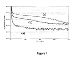
Figure 1 . Dynamic SIMS (secondary ion mass spectroscopy) Spectra for copper films pretreated with a hydrogen (H2) plasma then exposed to (a) no seconds of 5 % SiH4 in nitrogen, (b) 10 seconds of 5% SiH4 in nitrogen, and (c) 20 seconds of 5% SiH4 in nitrogen, samples (b) and (c) were also post treated with an NH3 plasma. -
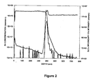
Figure 2 . Dynamic SIMS(secondary ion mass spectroscopy) data for a copper film pretreated with a hydrogen (H2) plasma, then exposed to 20 seconds of 9% Me4Sn in helium, post treated with a H2 plasma then capped with 400 nm of PECVD(Plasma Enhanced Chemical Vapor Deposition) Si3N4. -
Figure 3 . Dynamic SIMS (secondary ion mass spectroscopy) data for a copper film pretreated with a hydrogen (H2) plasma, then exposed to 20 seconds of CpCo(CO)2, post treated with hydrogen (H2) plasma then capped with 400 nm of PECVD Si3N4. -
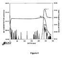
Figure 4 . Dynamic SIMS (secondary ion mass spectroscopy) data for a copper film pretreated with a hydrogen (H2) plasma, then exposed to 20 seconds of CpMn(CO)3, post treated with a hydrogen (H2) plasma then capped with 400 nm of PECVD Si3N4. -
Figure 5 . Dynamic SIMS (secondary ion mass spectroscopy) data for a copper film pretreated with a hydrogen (H2) plasma, then exposed to 20 seconds of EtCp2Ni, post treated with a hydrogen (H2) plasma then capped with 400 nm of PECVD Si3N4, -
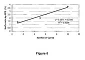
Figure 6 . X-ray photoelectron spectroscopy (XPS) data for the amount of tin at the copper surface presented as a ratio of Sn/Cu (%).
Copper adhesion to barrier layers and electromigration resistance are extremely important properties affecting device yield and device lifetimes. Currently the microelectronics industry is evaluating both silane exposure and electroless cobalt deposition to improve adhesion between the copper and the barrier dielectric layer. These are not optimal solutions as the silane treatments increase the copper resistivity which is a significant concern at the 32 nm generation and below, and the electroless cobalt deposition requires significant added steps to integrate.
The deposition of oxygen containing films directly onto copper generally does not result in highly adhesive interfaces due to the formation of copper oxide. Therefore dielectric barrier materials reported in the literature are generally silicon nitride or organosilicon carbonitride based materials, however, there is a desire in the microeletronics industry to use silicon oxide, organosilicon oxycarbide, organosilicon oxynitride, organosilicon carbonitride or organosilicon oxycarbonitride based films as barrier dielectrics because of their reduced dielectric constants. The method described in the present invention, that is, the use of certain volatile metallic materials as the adhesion promoter may allow for the deposition of oxygen-containing barrier films onto copper layers while retaining excellent adhesion properties. Metals under consideration are zinc, silver, chromium, tin, manganese, nickel, aluminum, and cobalt.
The organometallic precursor is preferably selected from the group consisting of tetramethyltin (Me4Sn), dibutyldimethyltin, tributyltin hydride, tin hydride (SnH4) and tin deuteride (SnD4), tetraalkyltin, trialkyltin hydride, dialkyltin dihydride, alkylalkoxytin, tetraalkoxytin, tetrakis(dialkylamino)tin, cyclopentadienyl cobalt dicarbonyl (CpCo(CO)2), nitrosyl cobalt pentacarbonyl, cyclopentadienyl manganese tricarbonyl (CpMn(CO)3), bis(ethylcyclopentadienyl)nickel ((EtCp)2Ni), dialkylzinc and amine adducts of dialkylzinc (e.g. diethylzinc (Et2Zn), diethylzinc-trimethylamine adduct, dimethylzinc), , nickel hexacarbonyl (Ni(CO)6), tungsten hexafluoride (WF6), chromium hexacarbonyl (Cr(CO)6), trimethylaluminum, dimethylethylamine alane (DMEAA), and tungsten hexacarbonyl (W(CO)6).
A delivery apparatus for the organometallic precursors in the present invention includes any container designed for safety delivery. A typical container comprises an interior volume bounded by interior wall, an inlet, and an outlet.
The specific pressurized apparatus and method disclosed inU.S. Pat. Nos. 7,013,916 can also be used in the present invention.
The organometallic precursor can be contained and delivered at sub-atmospheric pressure in a pressurized container, which includes- (a) a valve body in sealed communication with an outlet orifice of the pressurized container, said outlet orifice of said pressurized container open to an interior chamber of said pressurized container;
- (b) a fluid discharge path in the valve body, between the outlet orifice of the pressurized container and an outlet orifice of the valve body;
- (c) a pressure regulator having a pressure sensing means capable of responding to sub-atmospheric pressure, integral to said valve body, in-line in the fluid discharge path, said pressure regulator pre-set to a pressure below atmospheric pressure to allow said gas to be delivered through said regulator from said interior chamber only when said pressure sensing means senses a downstream pressure at or below said pre-set pressure; and
- (d) a high pressure shut-off valve integral to said valve body, in-line in the fluid discharge path and upstream from said pressure regulator; whereby said gas may flow through from said interior chamber of said pressurized container through said fluid discharge path, through said outlet orifice of said pressurized container, and through said outlet orifice of said valve body only when said outlet orifice is connected to a vacuum system.
- The deposition process used in the present invention can be any known process such as, Atomic Layer Deposition (ALD), Atomic Layer Treatment (ALT), Plasma Enhanced Atomic Layer Deposition (PEALD), Chemical Vapor Deposition(CVD), and Plasma Enhanced Chemical Vapor Deposition (PECVD), Low Pressure Chemical Vapor Deposition (LPCVD), Sub Atmospheric Chemical Vapor Deposition (SACVD), UV-assisted Chemical Vapor Deposition, Filament -assisted Chemical Vapor Deposition (FACVD), and Atmospheric Pressure Chemical Vapor Deposition (APCVD).
In the fabrication process, a direct liquid injection (DLI) delivery method can be employed. The precursor can be delivered by DLI of either a pure liquid precursor or by DLI of a mixture of the precursor with a solvent in a vessel or a container that is designed for the deposition delivery. A typical container comprises an interior volume bounded by interior wall, an inlet, and an outlet.
Organometallic precursors are vaporized either in the pure form or as mixtures, and the resulting precursor vapor, typically mixed with a carrier gas (such as argon, helium or nitrogen) is transported to a reactor, for example, a chemical vapor deposition (CVD) reactor.
More specifically, the organometallic precursor can comprise a solvent which solubilizes the organometallic precursor without decomposing it. The weight % of the solvent can be ranging from 5% to 99%; preferably 50% to 90%.
Suitable solvents can be simple hydrocarbons of the basic formula
CnH(2n+2-x); where n is 3-10 and x is equal to the number of cyclic structures or the degrees of unsaturation; for example, hexane, hexadiene, pentane, heptane, cyclohexane, cyclooctane or an aromatic hydrocarbon of the general structure
C6H(6-b)Rb where R can be 0-6 and can be the same or different, for example toluene, mesytelene, xylene, para-cymene and combinations thereof. The solvent should solubilise the organometallic precursor without decomposing the organometallic precursor.
Some organometallic precursors may also be soluble in oxygen containing solvents such as ethers, for example diethyl ether, methyl isobutyl ether, or tetrahydrofuran, alcohols, for example methanol, ethanol, or isopropanol, ketones for example acetone, aldehydes, or esters. Preferably, the oxygen containing solvent is selected from the group consisting of an ester, an alcohol and mixtures thereof. - Some of the advantages which may be available through the use of these solutions include the following:
- lowering the flammability of the mixture by choosing a solvent with a flammability lower than the organometallic;
- ability to delivery small amounts of organometallic precursor to the chamber using a dilute mixture;
- lowering the concentration of a potentially toxic organometallic precursor by dilution;
- an ability to tune the physical properties of the precursor solution such as viscosity for easy and safe delivery.
- (a) at least one patterned dielectric layer with embedded conductive metal features(such as copper or copper alloys);
- (b)an adhesion layer selectively deposited at least on the conductive metal features, said adhesion layer is selected from the group consisting of tin and zinc;
- (c)a dielectric barrier layer covering the at least one patterned dielectric layer with embedded conductive metal features having the adhesion layer.
- The structure can further have a metal barrier layer formed between the patterned dielectric layer and the embedded conductive metal features. The metal barrier layer preferably comprises materials such as tantalum, tantalum nitride, titanium, titanium nitride, cobalt, ruthenium, and other advanced barrier materials which prevent diffusion of the copper into the dielectric material.
- The following examples are provided for the purpose of further illustrating the present invention but are by no means intended to limit the same.
In the following examples, film treatments were carried out on an Applied Materials Precision-5000 system equipped to process 200 mm silicon wafers. Thermal treatments were carried out in a DxL vacuum chamber, organometallic precursors were delivered to the chamber either by vapor draw or entrained with helium as a carrier gas. Plasma treatments and deposition of silicon nitride films were carried out in a DxL vacuum chamber that was fitted with anAdvance Energy 200 rf generator. Adhesive energies were measured via 4-point bend using a DTS Company Delaminator instrument. Bulk film resistivity was measured on 100 nm thick copper films using a 4-point probe.
Silicon nitride cap layers were deposited using a standard Si3N4 deposition recipe: 100 sccm NH3, 75 sccm SiH4, 2000 sccm N2, 3.5 torr (470 Pa) chamber pressure, 400 mili-inch (1 cm) susceptor to wafer spacing, 300° C wafer temperature, and 300 W power.
Organometallic precursors evaluated were tetramethyltin (Me4Sn), cyclopentadienyl cobalt dicarbonyl (CpCo(CO)2), cyclopentadienyl manganese tricarbonyl (CpMn(CO)3), and bis(ethyl-cyclopentadienyl) nickel ((EtCp)2Ni).
Adhesion measurements are widely viewed as an acceptable surrogate measurement to predict performance in promoting electromigration resistance. Adhesion values were measured for copper films treated with various processes and capped with 400 nm of PEVCD Si3N4. 4-Point bend measurements were made by gluing a piece of silicon wafer on top of the Si3N4 film with epoxy, notching the top silicon wafer and using standard 4-point bend techniques. For examples 1 and 7 a 15 nm thick layer of chromium followed by a 150 nm thick layer of aluminum were deposited by sputtering onto both the silicon wafer and the Si3N4 in order to improve the adhesion strength of the epoxy.
In order to determine the adhesion value without any copper treatment a 400 nm thick layer of Si3N4 was deposited on top of a copper film that had not been treated, these films failed at the Si3N4 / copper interface with a value of 4.0 +/- 0.5 J/m2. - A series of films were exposed to 30 second hydrogen plasma to examine a baseline process for copper film pretreatment. In order to investigate the effect of a H2 plasma on adhesion, a copper film was treated with a 30 second H2 plasma followed by deposition of 400 nm of PECVD Si3N4.
Measurement of the adhesion with the 4-point bend technique revealed an adhesion value of 12.5 J/m2.
To examine the impact of a H2 plasma on the bulk resistivity of a copper film a 100 nm thick copper film with a bulk resistivity of 0.22 ohm-cm as measured by 4-point probe was exposed to a H2 plasma for 30 seconds after which time the bulk resistivity was measured as 0.19 ohm-cm. This decrease is presumably due to the reduction of a thin copper oxide layer on top of the copper. - The data was summarized in Tables I and II.
- In order to investigate the effect of a H2 plasma on a porous organosilicate glass (OSG), porous OSG PDEMS films were deposited by flowing a blend of diethoxymethylsilane (DEMS) and alpha terpinene into a vacuum chamber, striking a plasma to co-deposit an organosilicate glass (OSG) and a sacrificial organic porogen. This film is then annealed in using ultraviolet light to remove the sacrificial porogen to yield a porous OSG.
The porous OSG PDEMS films were then exposed to a 30 second H2 plasma. This resulted in a increase in the dielectric constant from 2.2 to 2.4, a increase in leakage current from 8 pico-amperes to 168 pico-amperes, and a minor change in breakdown voltage from ∼4 to 3.75 MV/m.
The data was summarized in Table III. - A series of films were exposed to a 30 second hydrogen plasma pre-treatment, followed by exposure to a mixture of 5% SiH4 in nitrogen at 4.5 torr (600 Pa) for a variable amount of time, and finally to a NH3 plasma for 30 seconds post-treatment as shown below, in order to examine a baseline process for copper treatment.
- 1) H2 plasma pre-treat to reduce CuO
300 sccm H2, 2.7 torr (360 Pa), 400 mil (1 cm) spacing, 300° C, at 300 W for 30 seconds - 2) SiH4 exposure
2000 sccm N2, 100 sccm SiH4, 4.5 Torr (600 Pa), 300° C for a variable length of time - 3) NH3 plasma post treatment
200 sccm NH3, 4.5 Torr (600 Pa), 300 mil (0.8 cm), 300° C, at 300 W for 30 seconds - 4) This may or may not have been followed with a Si3N4 capping layer.
- To examine the impact of the silane treatment on the bulk resistivity of a copper film a 100 nm thick copper film with a bulk resistivity of 0.21 ohm-cm as measured by 4-point probe was exposed to the silane treatment for 5 and 10 seconds with H2 plasma pre treatment and a NH3 plasma post treatment after which time the bulk resistivity was measured as 0.40 and 0.47 ohm-cm respectively. This sharp increase is believed to be due to silicon diffusing into the copper.
Similar samples with a thicker copper film were prepared and submitted for dynamic SIMS (secondary ion mass spectroscopy), the results of this analysis as well as that for a standard copper film exposed only to H2 plasma treatment are shown infigure 1 , it is evident that as the silane exposure times increased the amount of and depth of silicon diffusion also increased.
The data was summarized in Table II. - Measurement of the adhesion between a copper film which had been exposed to a H2 plasma pre-treatment, followed by a 10 second exposure to an organometallic precursor: 9% Me4Sn in He at 4.5 Torr (600 Pa) and 300° C then capped with a 400 nm film of PECVD Si3N4 was measured with the 4-point bend technique which yielding an adhesion value of 6.3 +/- 1 J/m2 with delamination occurring at the copper / Si3N4 interface. This indicates no improvement in adhesion relative to the untreated copper film.
The data was summarized in Table I. - In order to investigate the effect of a Me4Sn exposure on a porous organosilicate glass (OSG), the porous OSG deposited as described in Example 2 was exposed to an organometallic precursor: 9% mixture of Me4Sn in helium at 300° C for 20 seconds, this resulted in a increase in the dielectric constant from 2.2 to 2.3, a minor change in leakage current from ∼8 pico-amperes to 7 pico-amperes, and a minor change in breakdown voltage from ∼4 to 4.18 MV/m.
The last measurement was also repeated for the exposure to Me4Sn after a 30 second H2 plasma treatment. - Compared to the values measured above for a porous OSG PDEMS™ film exposed just to a H2 plasma treatment (Example 2), further exposure to 20 seconds of Me4Sn resulted in a minor change in the dielectric constant from 2.5 to 2.4, a minor change in leakage current from 166 pico-amperes to 230 pico-amperes, and a minor change in breakdown voltage from 3.76 to 3.62 MV/m.
The data was summarized in Table III. - Measurement of the adhesion between a sample which had been exposed to a H2 plasma followed by a 10 second exposure to 9% Me4Sn in He then treated with a H2 plasma post treatment and capped with a 400 nm film of PECVD Si3N4 was measured with the 4-point bend technique described previously which yielded an adhesion value of 22.0J/m2. The delamination occurred at the copper / Si3N4 interface.
To examine the impact of this Me4Sn treatment on the bulk resistivity of acopper film 100 nm thick copper films with bulk resistivities of 0.22 and 0.20 ohm-cm as measured by 4-point probe were exposed to the Me4Sn treatment for 10 and 20 seconds with H2 plasma pre and post treatments after which time the bulk resistivity was measured as 0.18 and 0.17 ohm-cm respectively. This decrease in resistivity is believed to be due to a combination of (1) reduction of the CuO layer with the H2 plasma pretreatment and (2) a relatively low resistivity of the thin adhesion layer deposited by the Me4Sn.
The data was summarized in Table I and II.
Similar samples with a thicker copper film were prepared and submitted for dynamic SIMS (secondary ion mass spectroscopy). These films were treated with a 20 second exposure to 9% Me4Sn in helium with pre and post H2 plasma treatments then capped with a 400 nm thick PECVD Si3N4 layer.
The result of the analysis is shown inFigure 2 . It is evident that the Me4Sn exposure results in the deposition of a thin tin containing layer at the interface between the copper and the Si3N4.
A set of wafers were obtained on which patterned Black Diamond™ organosilicate glass films were filled with copper metal. These patterned features included Kelvin structures of varying line widths (0.14 - 0.18 microns) to measure copper line resistance and comb-serpentine structures (0.16 x 0.18 microns) to evaluate leakage current and electrical shorting. These wafers were first treated with a hydrogen plasma at 350 ºC for 20 seconds to reduce the surface copper oxide, these were then exposed to tetramethyltin for 30 seconds at 350 ºC followed by a second hydrogen plasma to remove residual carbon from the surface. These wafers were then electrically probed to test for leakage current and electrical shorts as well as measuring copper line resistance.
Testing of the Kelvin structures revealed that the copper line resistance was not increased by treatment with tetramethyltin which indicates that the treatment with tetramethyltin results in only a surface treatment. If the tin had diffused into the copper an increase in copper resistance would have been observed. Testing of the Comb-Serpentine structures revealed that the treatment with tetramethyltin does not increase the line to line leakage current and no electrical shorts were observed indicating that the tetramethyltin treatment does not deposit a conductive layer of tin on the Organosilicate Glass supporting the fact of selective treatment of the copper surface with tetramethyltin. Additionally there was no increase in capacitance between metal lines which indicates that the tetramethyltin treatment does not damage the organosilicate glass. - Measurement of the adhesion between a sample which had been exposed to a H2 plasma followed by a 10 second exposure to vapors of CpCo(CO)2 at 300° C then treated with a H2 plasma post treatment and capped with a 400 nm film of PECVD Si3N4 was measured with the 4-point bend technique yielding an adhesion value of 17.5 J/m2. However, the delamination occurred between the top of the Si3N4 and the bare silicon used in the 4-point bend technique, therefore the adhesion strength of the copper / Si3N4 interface could not be unambiguously measured.
The data was summarized in Table I.
Similar samples with a copper film exposed to the cobalt treatment were prepared and submitted for dynamic SIMS (secondary ion mass spectroscopy), these films were treated with a 20 second exposure to CpCo(CO)2 vapors at 300° C with pre and post H2 plasma treatments then capped with a 400 nm thick PECVD Si3N4 layer. - The result of the analysis is shown in
Figure 3 . It is evident that the CpCo(CO)2 exposure results in the deposition of a thin cobalt containing layer at the interface between the copper and the Si3N4. - Measurement of the adhesion between a sample which had been exposed to a H2 plasma followed by a 10 second exposure to vapors of CpMn(CO)3 at 300° C then treated with a H2 plasma post treatment and capped with a 400 nm film of PECVD Si3N4 was measured with the 4-point bend technique yielding an adhesion value of 21.9 +/- 2.3 J/m2. However, the delamination occurred between the top of the Si3N4 and the bare silicon used in the 4-point bend technique, therefore the adhesion strength of the copper / Si3N4 interface could not be unambiguously measured. The data was summarized in Table I.
Similar samples with a copper film exposed to the manganese treatment were prepared and submitted for dynamic SIMS (secondary ion mass spectroscopy), these films were treated with a 20 second exposure to CpMn(CO)3 vapors at 300° C with pre and post H2 plasma treatments then capped with a 400 nm thick PECVD Si3N4 layer.
The result of the analysis is shown inFigure 4 . It is evident that the CpMn(CO)3 exposure results in the deposition of a thin manganese containing layer at the interface between the copper and the Si3N4. - Measurement of the adhesion between a sample which had been exposed to a H2 plasma followed by a 10 second exposure to vapors of EtCp2Ni at 300°C then treated with a H2 plasma post treatment and capped with a 400 nm film of PECVD Si3N4 was measured with the 4-point bend technique yielding an adhesion value of 31.5 J/m2. However, the delamination occurred between the top of the Si3N4 and the bare silicon used in the 4-point bend technique, therefore the adhesion strength of the copper / Si3N4 interface could not be unambiguously measured.
The data was summarized in Table I. - Similar samples with a copper film exposed to the manganese treatment were prepared and submitted for dynamic SIMS (secondary ion mass spectroscopy), these films were treated with a 20 second exposure to EtCp2Ni vapors at 300° C with pre and post H2 plasma treatments then capped with a 400 nm thick PECVD Si3N4 layer.
The result of the analysis is shown inFigure 5 . It is evident that the EtCp2Ni exposure results in the deposition of a thin nickel containing layer at the interface between the copper and the Si3N4.
The data from above measurements are summarized in Table I.Table I. Effect of Process on Adhesion between PECVD Si3N4 and Copper Process Adhesion (J/m2) Untreated Film 4 +/- 0.5 H2 Treatment 12.5 Me4Sn with out Post 6.3 +/- 1.0 20 second Me4Sn with H2 Post 22.0 CpMn(CO)3 with H2 Post 21.9 +/- 2.3 (EtCp)2Ni with H2 post 31.5 CpCo(CO)2 with H2 post 17.5 - Table I shows the effect of various processes on the adhesion between the copper layer and the capping PECVD deposited Si3N4. These measurements were carried out by the industry standard 4-point bend technique. Unless otherwise noted all films were pretreated with a hydrogen plasma.
The untreated copper film shows a low adhesion value of 4 +/- 0.5 J/m2 with delamination at the Si3N4 to copper interface due to the poor adhesion to the native oxide found on copper films. Treatment with hydrogen plasma will reduce the copper oxide back to copper metal and an adhesion value of 12.6 J/m2 is measured with failure observed between the Si3N4 and the copper interface.
Treatment of the copper with a hydrogen plasma followed by a 10 second exposure to Me4Sn with no post treatment followed by capping with a PECVD Si3N4 layer results in an adhesion value of 6.3 J/m2 with delamination at the Si3N4 to copper interface which is believed to be due to residual carbon at the surface after treatment with the Me4Sn. Treatment with hydrogen plasma after exposure the Me4Sn improves adhesion dramatically and an adhesion value of 22.0 J/m2 is observed with delamination occurring at the Si3N4 / copper interface. Copper films treated with cyclopentadienylmanganese tricarbonyl, bis(ethylcyclopentadienyl)nickel, and cyclopentadienylcobalt dicarbonyl vapors followed by a hydrogen plasma treatment were not examined with the advanced 4-point bend technique in which chromium and aluminum layer deposition and thus delamination occurred at the epoxy interface which indicates good adhesion although accurate measurements were not possible.Table II. Effect of copper treatments on bulk copper resistivity Treatment Resistivity before treatment (10-3ohm-cm) Resistivity after treatment (10-3ohm-cm) Change in resistivity (%) H2 plasma only 224 +/- 4 186 +/- 4 -17 NH3 plasma only 182 +/- 2 167 +/- 2 -8 H2 plasma / 5 second SiH4 / NH3 plasma 214 +/- 4 402 +/- 30 89 H2 plasma / 10 second SiH4 / NH3 plasma 210 +/- 4 46 +/- 26 122 H2 plasma / 10 second Me4Sn / H2 plasma 221 +/- 4 185 +/- 1 -16 H2 plasma / 20 second Me4Sn / H2 plasma 200 +/- 8 174 +/- 6 -13 - Table II shows the effect of various copper treatments on the bulk resistivity of a 100nm thick copper film as measured by 4-point probe before and after treatment. All treatments were carried out at 300° C. Exposure of the copper films to just hydrogen or ammonia plasmas lower the bulk resistivity by 8 to 17% presumably due to reduction of the native copper oxide layer found on top of the untreated films. Exposure of the copper to either 5 or 10 seconds of SiH4 in the "standard silane process" results in significant bulk resistivity increases of 89 and 122% respectively, presumably due to formation of CuSiN and diffusion of Si into the bulk of the copper. Exposure of the copper layer to Me4Sn for either 10 or 20 seconds with pre and post hydrogen plasma treatments results in decrease the bulk resistivity by 16 and 13% respectively. These changes are similar to those measured for just hydrogen plasma only treatments, which indicates that the layer which is deposited from the Me4Sn exposure does not significantly impact the copper resistivity as is seen with silane exposure.
Table III. Effect of Me4Sn treatment on porous OSG films (PDEMS™) Treatment Dielectric Constant Leakage Current (pA) Breakdown Voltage (MV/m) Untreated ∼2.2 ∼8 ∼4 10 second Me4Sn 2.28 7 4.18 H2 plasma only 2.46 166 3.75 H2 plasma / 10 second Me4Sn 2.44 137 3.62 H2 plasma / 20 second Me4Sn 2.44 230 3.62 - Table III shows the effect of Me4Sn on the electrical performance of porous organosilicate films such as those produced by PDEMS™ ILD deposition process with a dielectric constant of ∼2.2. This experiment was performed to determine if the Me4Sn would diffuse into the pores of a porous OSG potentially degrading the electrical performance of the porous OSG. A PDEMS™ film with a measured dielectric constant of ∼2.2 was exposed to Me4Sn for 10 seconds at 300° C. The dielectric constant, leakage current and breakdown voltages are either unaffected or only minimally affected by exposure to the Me4Sn. These measurements were also run after exposure of the PDEMS™ to a hydrogen plasma and the values are given. The hydrogen plasma results in a increase in dielectric constant and leakage current. Exposure of the hydrogen plasma treated films to Me4Sn for 10 and 20 seconds does not significantly affect the dielectric constant or breakdown voltage. There is a measured difference in leakage current upon exposure to the Me4Sn. However, we do not believe that the measured differences are significant.
- This example repeated the same measurement as set in Example 7, but with various exposure times and temperatures.
Samples of copper films were first in-situ plasma treated with a H2 plasma to reduce the surface copper oxide (pre-treatment), after which the samples were exposed to tetramethyltin (Me4Sn) as a 9% mixture in helium for various exposure times and temperatures. The samples were once again exposed to a H2 plasma to remove surface carbon (post-treatment). Samples were then submitted for surface X-ray photoelectron spectroscopy (XPS) analysis to measure the Tin on the copper films. The percent tin was measured as a ratio relative to copper.
Table IV shows that for all exposures only a small amount of tin was deposited. If it is assumed that a monolayer of tin would be result in a XPS signal of ∼5 atomic % these samples have slightly less than a monolayer of tin on the surface. The observation that a film exposed for 20 seconds and a film exposed for 80 seconds had essentially the same level of tin indicates that this is a surface limited reaction and not a continual deposition reaction. This is further indicated by the sample which was exposed at 350 ºC which also showed essentially the same level of tin indicating that the deposition is not thermally driven.Table IV. Process % Sn/Cu by XPS 20 second exposure to Me4Sn at 300 C 1.4 80 second exposure to Me4Sn at 300 C 0.8 20 second exposure to Me4Sn at 350 1.1 - Next, three samples of copper films were first treated with a H2 plasma, then exposed to Me4Sn for 20 seconds followed by a H2 plasma. The above whole process was repeated 5 times and 10 times respectively on two of the three samples. The samples were then submitted for surface X-ray photoelectron spectroscopy (XPS) analysis to measure the tin on the copper surface. The percent tin was measured as a ration relative to copper.
As shown infigure 6 , the amount of tin increased from 1.4%, to 2.0% and finally 3.4% for one, five and ten process cycles, respectively. The whole process can be repeated until a desired thickness of the tin on the copper surface is achieved. This indicates that the ALD process can also be used to deposit tin onto the copper surface.
Samples of wafers with PDEMS and Si3N4 films on them were exposed to the same process described above for five cycles. Then, the sample was submitted for surface X-ray photoelectron spectroscopy (XPS) analysis to measure the Tin on the surfaces of PDEMS and Si3N4 films. There was no tin observed above the detection limit of the XPS, indicating that the Me4Sn process is a selective deposition process. - A mixture of 5 mL tetramethyltin along with 95 mL anhydrous hexane was prepared in a drybox. This mixture was then delivered to the CVD chamber by means of direct liquid injection of the mixture with a vaporization temperature of 50°C.
Copper films were first treated with a H2 plasma to reduce the copper oxide followed by exposure of the film to vapors of the tetramethyltin / hexane mixture at 350°C for 30 seconds after which time the films were post-treated with a NH3 plasma and finally coated with a Silicon carbon nitride film.
Analysis of the resulting film stack by x-ray photoelectron spectroscopy shows a clean metallic tin layer at the copper / silicon carbonitride interface. The use of a solvent such as hexane which does not influence the tin treatment offers advantages in safety and handling. - The foregoing examples and description of the preferred embodiments should be taken as illustrating, rather than as limiting the present invention as defined by the claims. As will be readily appreciated, numerous variations and combinations of the features set forth above can be utilized without departing from the present invention as set forth in the claims. Such variations are not regarded as a departure from the scope of the invention, and all such variations are intended to be included within the scope of the following claims.
The dielectric barrier layer materials such as silicon nitride, silicon oxide, silicon carbide, silicon oxycarbide, silicon oxynitride, silicon carbonitride, silicon oxycarbonitride and mixtures are considered, where the "silicon" includes "organosilicon". For example, the list of materials includes organosilicon oxycarbide, organosilicon oxynitride, organosilicon carbonitride, organosilicon oxycarbonitride and mixtures. The barrier layer preferably has a dielectric constant of less than 7. An example of dielectric barrier layer material is a Si3N4.
A consideration here is that the metal or the organometallic precursor should not negatively impact the dielectric materials exposed to the same processing. Examples of dielectric materials include silicon dioxide, fluorosilicate glass (FSG), organosilicate glass (OSG), aka carbon doped oxide (CDO), or porous low-k dielectric materials. Examples of low k dielectric materials used in the integration scheme include porous OSG (organosilicate glass) materials such as those deposited from PDEMS™ interlayer dielectric (ILD) deposition process. The low k dielectric materials usually have a dielectric constant of less than 3.0. The dielectric material preferably has a dielectric constant of less than 3.2.
With the materials considered above together, a structure having improved conductive metal adhesion to a barrier layer and electromigration resistance is formed in the present invention. The structure comprises:
Claims (15)
- A method of processing a semiconductor device comprising steps of:(a) providing a substrate in a processing chamber;
wherein the substrate comprises at least one patterned dielectric layer and at least one patterned conductive metal layer; and(b) introducing an organometallic precursor to the processing chamber to selectively deposit an adhesion layer at least on the at least one patterned conductive metal layer;wherein the organometallic precursor is selected from the group consisting of organozinc, organosilver, organochromium, organotin, organomanganese, organonickel, organocobalt, organoaluminum, and mixtures thereof. - The method in Claim 1 further comprising a step (ab) before (b) of exposing the substrate to a pre-treatment.
- The method in Claim 2, wherein steps (ab) and (b) are repeated until a desired thickness of the adhesion layer is achieved.
- The method in any one of the preceding claims further comprising a step (c) of depositing a dielectric barrier layer on the substrate having the adhesion layer.
- The method in Claim 4 further comprising a step before (c) of exposing the substrate having the adhesion layer to a post-treatment.
- The method in Claim 4 or Claim 5, wherein the dielectric barrier layer is selected from the group consisting of: silicon nitride, silicon oxide, silicon oxycarbide, silicon oxynitride, silicon carbonitride, silicon oxycarbonitride, silicon carbide, and mixtures thereof.
- The method in any one of Claims 2 to 6 , wherein the pre-treatment and/or post-treatment is selected from the group consisting of H2 plasma, NH3 plasma, H2/He plasma, H2/N2 plasma and mixtures thereof.
- The method in any one of the preceding claims, wherein the organometallic precursor is solubilized in a solvent selected from the group consisting of a hydrocarbon with formula CnH(2n+2-x); where n is 3-10 and x is equal to the number of cyclic structures or the degrees of unsaturation; an oxygen containing solvent; and mixtures thereof;
wherein the solvent solubilizes the organometallic precursor without decomposing the organometallic precursor. - The method in any one of the preceding claims, wherein the organometallic precursor is contained and delivered at sub-atmospheric pressure in a pressurized container, comprising(a) a valve body in sealed communication with an outlet orifice of the pressurized container, said outlet orifice of said pressurized container being open to an interior chamber of said pressurized container;(b) a fluid discharge path in the valve body, between the outlet orifice of the pressurized container and an outlet orifice of the valve body;(c) a pressure regulator having a pressure sensing means capable of responding to sub-atmospheric pressure, integral to said valve body, in-line in the fluid discharge path, said pressure regulator being pre-set to a pressure below atmospheric pressure to allow said gas to be delivered through said regulator from said interior chamber only when said pressure sensing means senses a downstream pressure at or below said pre-set pressure; and(d) a high pressure shut-off valve integral to said valve body, in-line in the fluid discharge path and upstream from said pressure regulator; whereby said gas may flow through from said interior chamber of said pressurized container through said fluid discharge path, through said outlet orifice of said pressurized container, and through said outlet orifice of said valve body only when said outlet orifice is connected to a vacuum system.
- The method in any one of the preceding claims, wherein the organometallic precursor is selected from the group consisting of tetramethyltin (Me4Sn), dibutyldimethyltin, tributyltin hydride, tetraalkyltin, trialkyltin hydride, dialkyltin dihydride, alkylalkoxytin, tetraalkoxytin, tetrakis(dialkylamino)tin, tin hydride (SnH4), tin deuteride (SnD4), cyclopentadienyl cobalt dicarbonyl (CpCo(CO)2), nitrosyl cobalt pentacarbonyl, cyclopentadienyl manganese tricarbonyl (CpMn(CO)3), bis(ethylcyclopentadienyl)nickel ((EtCp)2Ni), diethylzinc (Et2Zn), diethylzinc-trimethylamine adduct, dimethylzinc, dialkylzinc, amine adducts of dialkylzinc, nickel hexacarbonyl (Ni(CO)6), tungsten hexafluoride (WF6), chromium hexacarbonyl (Cr(CO)6), trimethylaluminum, dimethylethylamine alane (DMEAA), tungsten hexacarbonyl (W(CO)6), and mixtures thereof.
- The method in any one of the preceding claims, wherein the adhesion layer is selected from the group consisting of tin and zinc.
- A structure comprising :(a) at least one patterned dielectric layer and at least one patterned conductive metal layer;(b)an adhesion layer selectively deposited at least on the at least one patterned conductive metal layer, said adhesion layer is selected from the group consisting of tin and zinc; and(c)a dielectric barrier layer covering the at least one patterned dielectric layer and the at least one patterned conductive metal layer having the adhesion layer.
- The structure of Claim 12 wherein a metal barrier layer is formed between the at least one patterned dielectric layer and the at least one patterned conductive metal layer.
- The structure of Claim 13 wherein the metal barrier layer is selected from the group consisting of tantalum, tantalum nitride, titanium, titanium nitride, cobalt, ruthenium, and mixtures thereof.
- An article of manufacture comprisingorganotin;a solvent selected from the group consisting of a hydrocarbon with formula CnH(2n+2-x); where n is 3-10 and x is equal to the number of cyclic structuresor the degrees of unsaturation; an oxygen containing solvent; and combinations thereof; anda container comprising an interior volume bounded by interior wall, an inlet, and an outlet;
wherein the organotin is solubilized in the solvent, and a mixture of the organotin and the solvent is contained and delivered in the container.
Applications Claiming Priority (3)
| Application Number | Priority Date | Filing Date | Title |
|---|---|---|---|
| US3887408P | 2008-03-24 | 2008-03-24 | |
| US7484308P | 2008-06-23 | 2008-06-23 | |
| US12/406,467 US8043976B2 (en) | 2008-03-24 | 2009-03-18 | Adhesion to copper and copper electromigration resistance |
Publications (4)
| Publication Number | Publication Date |
|---|---|
| EP2105960A2 true EP2105960A2 (en) | 2009-09-30 |
| EP2105960A3 EP2105960A3 (en) | 2012-04-04 |
| EP2105960B1 EP2105960B1 (en) | 2017-08-02 |
| EP2105960B8 EP2105960B8 (en) | 2017-10-11 |
Family
ID=40793197
Family Applications (1)
| Application Number | Title | Priority Date | Filing Date |
|---|---|---|---|
| EP09155899.9A Active EP2105960B8 (en) | 2008-03-24 | 2009-03-23 | Improved adhesion to copper and copper electromigration resistance |
Country Status (6)
| Country | Link |
|---|---|
| US (1) | US8043976B2 (en) |
| EP (1) | EP2105960B8 (en) |
| JP (1) | JP5266116B2 (en) |
| KR (2) | KR101169501B1 (en) |
| CN (1) | CN101609810B (en) |
| TW (1) | TWI479567B (en) |
Cited By (1)
| Publication number | Priority date | Publication date | Assignee | Title |
|---|---|---|---|---|
| WO2012054688A2 (en) * | 2010-10-22 | 2012-04-26 | Applied Materials, Inc. | Methods for enhancing tantalum filament life in hot wire chemical vapor deposition processes |
Families Citing this family (13)
| Publication number | Priority date | Publication date | Assignee | Title |
|---|---|---|---|---|
| JP5530118B2 (en) * | 2009-04-08 | 2014-06-25 | 東京エレクトロン株式会社 | Method for forming manganese oxide film, method for manufacturing semiconductor device, and semiconductor device |
| JP2013213269A (en) * | 2012-04-04 | 2013-10-17 | Tokyo Electron Ltd | Film forming method and storage medium |
| KR101715964B1 (en) | 2012-06-04 | 2017-03-13 | 삼성에스디아이 주식회사 | Rechargeable secondary battery |
| US11761086B2 (en) * | 2014-02-23 | 2023-09-19 | Entegris, Inc. | Cobalt precursors |
| US9673042B2 (en) | 2015-09-01 | 2017-06-06 | Applied Materials, Inc. | Methods and apparatus for in-situ cleaning of copper surfaces and deposition and removal of self-assembled monolayers |
| KR102019468B1 (en) * | 2016-11-29 | 2019-09-06 | 주식회사 엘지화학 | Adhesive film for semiconductor device and semiconductor device |
| WO2018169543A1 (en) * | 2017-03-17 | 2018-09-20 | Intel Corporation | Dielectric film with pressure sensitive microcapsules of adhesion promoter |
| CA2975104A1 (en) | 2017-08-02 | 2019-02-02 | Seastar Chemicals Inc. | Organometallic compounds and methods for the deposition of high purity tin oxide |
| US10580645B2 (en) * | 2018-04-30 | 2020-03-03 | Asm Ip Holding B.V. | Plasma enhanced atomic layer deposition (PEALD) of SiN using silicon-hydrohalide precursors |
| JP7213642B2 (en) * | 2018-09-05 | 2023-01-27 | 東京エレクトロン株式会社 | Method for manufacturing resist film |
| US11769692B2 (en) | 2018-10-31 | 2023-09-26 | Taiwan Semiconductor Manufacturing Co., Ltd. | High breakdown voltage inter-metal dielectric layer |
| JP7345787B2 (en) * | 2020-04-30 | 2023-09-19 | 東京エレクトロン株式会社 | Selective film formation method |
| US20230109501A1 (en) * | 2021-09-28 | 2023-04-06 | Applied Materials, Inc. | Tungsten gapfill using molybdenum co-flow |
Citations (5)
| Publication number | Priority date | Publication date | Assignee | Title |
|---|---|---|---|---|
| WO2001008213A1 (en) | 1999-07-27 | 2001-02-01 | International Business Machines Corporation | REDUCED ELECTROMIGRATION AND STRESS INDUCED MIGRATION OF Cu WIRES BY SURFACE COATING |
| US7013916B1 (en) | 1997-11-14 | 2006-03-21 | Air Products And Chemicals, Inc. | Sub-atmospheric gas delivery method and apparatus |
| US7153774B2 (en) | 2002-06-06 | 2006-12-26 | Intel Corporation | Method of making a semiconductor device that has copper damascene interconnects with enhanced electromigration reliability |
| US7193325B2 (en) | 2004-04-30 | 2007-03-20 | Taiwan Semiconductor Manufacturing Company, Ltd. | Reliability improvement of SiOC etch with trimethylsilane gas passivation in Cu damascene interconnects |
| US7229911B2 (en) | 2004-04-19 | 2007-06-12 | Applied Materials, Inc. | Adhesion improvement for low k dielectrics to conductive materials |
Family Cites Families (29)
| Publication number | Priority date | Publication date | Assignee | Title |
|---|---|---|---|---|
| JPH07161034A (en) | 1993-04-13 | 1995-06-23 | Matsushita Electric Ind Co Ltd | Magnetic recording medium |
| US6444264B2 (en) | 1995-03-31 | 2002-09-03 | Advanced Technology Materials, Inc. | Method for liquid delivery CVD utilizing alkane and polyamine solvent compositions |
| GB9724168D0 (en) * | 1997-11-14 | 1998-01-14 | Air Prod & Chem | Gas control device and method of supplying gas |
| US6147000A (en) | 1998-08-11 | 2000-11-14 | Advanced Micro Devices, Inc. | Method for forming low dielectric passivation of copper interconnects |
| US6355571B1 (en) * | 1998-11-17 | 2002-03-12 | Applied Materials, Inc. | Method and apparatus for reducing copper oxidation and contamination in a semiconductor device |
| US6479389B1 (en) | 1999-10-04 | 2002-11-12 | Taiwan Semiconductor Manufacturing Company | Method of doping copper metallization |
| US6984591B1 (en) * | 2000-04-20 | 2006-01-10 | International Business Machines Corporation | Precursor source mixtures |
| US6645550B1 (en) * | 2000-06-22 | 2003-11-11 | Applied Materials, Inc. | Method of treating a substrate |
| US20020048926A1 (en) * | 2000-09-14 | 2002-04-25 | Konecni Anthony J. | Method for forming a self-aligned copper capping diffusion barrier |
| US7351449B2 (en) | 2000-09-22 | 2008-04-01 | N Gimat Co. | Chemical vapor deposition methods for making powders and coatings, and coatings made using these methods |
| US20020089063A1 (en) * | 2001-01-08 | 2002-07-11 | Ahn Kie Y. | Copper dual damascene interconnect technology |
| US6518167B1 (en) * | 2002-04-16 | 2003-02-11 | Advanced Micro Devices, Inc. | Method of forming a metal or metal nitride interface layer between silicon nitride and copper |
| US6846515B2 (en) | 2002-04-17 | 2005-01-25 | Air Products And Chemicals, Inc. | Methods for using porogens and/or porogenated precursors to provide porous organosilica glass films with low dielectric constants |
| KR100443796B1 (en) | 2002-06-29 | 2004-08-11 | 주식회사 하이닉스반도체 | Method for forming a copper metal line |
| JP3992588B2 (en) * | 2002-10-23 | 2007-10-17 | 東京エレクトロン株式会社 | Deposition method |
| CN100345999C (en) * | 2003-01-02 | 2007-10-31 | 上海华虹(集团)有限公司 | Process for chemical vapor phase depositing titaniam nitride containing silicon using titanium containing organic metal material |
| KR100974778B1 (en) | 2003-06-30 | 2010-08-06 | 삼성전자주식회사 | Organometallic Precursor Composition for Metal Film or Patterns and a Method for preparing Metal film or Patterns by using the same |
| KR100546209B1 (en) | 2003-07-09 | 2006-01-24 | 매그나칩 반도체 유한회사 | Copper wiring formation method of semiconductor device |
| US6979625B1 (en) | 2003-11-12 | 2005-12-27 | Advanced Micro Devices, Inc. | Copper interconnects with metal capping layer and selective copper alloys |
| FR2868085B1 (en) | 2004-03-24 | 2006-07-14 | Alchimer Sa | METHOD FOR SELECTIVE COATING OF COMPOSITE SURFACE, FABRICATION OF MICROELECTRONIC INTERCONNECTIONS USING THE SAME, AND INTEGRATED CIRCUITS |
| FR2868709B1 (en) | 2004-04-08 | 2006-06-23 | Rexam Dispensing Systems Sas | NON-RETURN AIR DISTRIBUTOR FOR THE DELIVERY OF LOW DOSES OF LIQUID PRODUCTS AND, IN PARTICULAR, OF COSMETIC OR PHARMACEUTICAL PRODUCTS |
| JP2006063386A (en) | 2004-08-26 | 2006-03-09 | Tokyo Electron Ltd | Method for producing semiconductor device |
| US7332445B2 (en) | 2004-09-28 | 2008-02-19 | Air Products And Chemicals, Inc. | Porous low dielectric constant compositions and methods for making and using same |
| US7476618B2 (en) * | 2004-10-26 | 2009-01-13 | Asm Japan K.K. | Selective formation of metal layers in an integrated circuit |
| US7247946B2 (en) | 2005-01-18 | 2007-07-24 | International Business Machines Corporation | On-chip Cu interconnection using 1 to 5 nm thick metal cap |
| JP5116251B2 (en) * | 2005-05-20 | 2013-01-09 | 株式会社半導体エネルギー研究所 | Method for manufacturing semiconductor device |
| JP2007035734A (en) * | 2005-07-25 | 2007-02-08 | Nec Electronics Corp | Semiconductor device and manufacturing method thereof |
| TW200802703A (en) * | 2005-11-28 | 2008-01-01 | Nxp Bv | Method of forming a self aligned copper capping layer |
| US20070299239A1 (en) | 2006-06-27 | 2007-12-27 | Air Products And Chemicals, Inc. | Curing Dielectric Films Under A Reducing Atmosphere |
-
2009
- 2009-03-18 US US12/406,467 patent/US8043976B2/en active Active
- 2009-03-20 TW TW098109291A patent/TWI479567B/en active
- 2009-03-23 EP EP09155899.9A patent/EP2105960B8/en active Active
- 2009-03-24 JP JP2009072147A patent/JP5266116B2/en not_active Expired - Fee Related
- 2009-03-24 KR KR1020090025008A patent/KR101169501B1/en active IP Right Grant
- 2009-03-24 CN CN200910138735.XA patent/CN101609810B/en active Active
-
2011
- 2011-01-17 KR KR1020110004600A patent/KR20110019398A/en not_active Application Discontinuation
Patent Citations (5)
| Publication number | Priority date | Publication date | Assignee | Title |
|---|---|---|---|---|
| US7013916B1 (en) | 1997-11-14 | 2006-03-21 | Air Products And Chemicals, Inc. | Sub-atmospheric gas delivery method and apparatus |
| WO2001008213A1 (en) | 1999-07-27 | 2001-02-01 | International Business Machines Corporation | REDUCED ELECTROMIGRATION AND STRESS INDUCED MIGRATION OF Cu WIRES BY SURFACE COATING |
| US7153774B2 (en) | 2002-06-06 | 2006-12-26 | Intel Corporation | Method of making a semiconductor device that has copper damascene interconnects with enhanced electromigration reliability |
| US7229911B2 (en) | 2004-04-19 | 2007-06-12 | Applied Materials, Inc. | Adhesion improvement for low k dielectrics to conductive materials |
| US7193325B2 (en) | 2004-04-30 | 2007-03-20 | Taiwan Semiconductor Manufacturing Company, Ltd. | Reliability improvement of SiOC etch with trimethylsilane gas passivation in Cu damascene interconnects |
Cited By (2)
| Publication number | Priority date | Publication date | Assignee | Title |
|---|---|---|---|---|
| WO2012054688A2 (en) * | 2010-10-22 | 2012-04-26 | Applied Materials, Inc. | Methods for enhancing tantalum filament life in hot wire chemical vapor deposition processes |
| WO2012054688A3 (en) * | 2010-10-22 | 2012-06-07 | Applied Materials, Inc. | Methods for enhancing tantalum filament life in hot wire chemical vapor deposition processes |
Also Published As
| Publication number | Publication date |
|---|---|
| US20090236745A1 (en) | 2009-09-24 |
| CN101609810B (en) | 2014-06-04 |
| EP2105960A3 (en) | 2012-04-04 |
| KR101169501B1 (en) | 2012-07-27 |
| KR20110019398A (en) | 2011-02-25 |
| JP2009239283A (en) | 2009-10-15 |
| CN101609810A (en) | 2009-12-23 |
| KR20090101859A (en) | 2009-09-29 |
| TW200945440A (en) | 2009-11-01 |
| TWI479567B (en) | 2015-04-01 |
| EP2105960B8 (en) | 2017-10-11 |
| EP2105960B1 (en) | 2017-08-02 |
| JP5266116B2 (en) | 2013-08-21 |
| US8043976B2 (en) | 2011-10-25 |
Similar Documents
| Publication | Publication Date | Title |
|---|---|---|
| EP2105960B1 (en) | Improved adhesion to copper and copper electromigration resistance | |
| US6380080B2 (en) | Methods for preparing ruthenium metal films | |
| US6037001A (en) | Method for the chemical vapor deposition of copper-based films | |
| Kwon et al. | Atomic layer deposition of ruthenium thin films for copper glue layer | |
| US9111761B2 (en) | Multi component dielectric layer | |
| EP2692897B1 (en) | Methods of forming non-oxygen containing silicon-based films | |
| US8293001B2 (en) | Porogens, porogenated precursors and methods for using the same to provide porous organosilica glass films with low dielectric constants | |
| US7799671B1 (en) | Interfacial layers for electromigration resistance improvement in damascene interconnects | |
| US7943195B2 (en) | Porogens, porogenated precursors and methods for using the same to provide porous organosilica glass films with low dielectric constants | |
| CN105304479B (en) | For the self-aligned barrier layers and capping layer of interconnection | |
| US6066196A (en) | Method for the chemical vapor deposition of copper-based films and copper source precursors for the same | |
| US6281125B1 (en) | Methods for preparing ruthenium oxide films | |
| US6846515B2 (en) | Methods for using porogens and/or porogenated precursors to provide porous organosilica glass films with low dielectric constants | |
| EP1115900B1 (en) | Methods for preparing ruthenium metal films | |
| EP2251899B1 (en) | Dielectric barrier deposition using nitrogen containing precursor | |
| Hinz et al. | Analysis of NbN thin film deposition by plasma-enhanced ALD for gate electrode application | |
| Lu et al. | A new process for depositing tungsten nitride thin films | |
| Papadimitropoulos et al. | Copper Films Deposited by Hot‐Wire CVD and Direct Liquid Injection of CupraSelect | |
| Martini | Metallization and modification of low-k dielectric materials | |
| Wojcik et al. | A comparative study of thermal and plasma enhanced ALD Ta-NC films on SiO 2, SiCOH and Cu substrates | |
| Kim et al. | Properties of chemically vapor deposited blanket tungsten films on tin glue layers prepared by chemical vapor deposition | |
| Gatineau et al. | A New Liquid Precursor for Pure Ruthenium Depositions | |
| US20120328798A1 (en) | Inter-low-permittivity layer insulating film, and method for forming inter-low-permittivity layer insulating film | |
| Barton | Chemical vapor deposition and atomic layer deposition of metal oxide and nitride thin films |
Legal Events
| Date | Code | Title | Description |
|---|---|---|---|
| PUAI | Public reference made under article 153(3) epc to a published international application that has entered the european phase |
Free format text: ORIGINAL CODE: 0009012 |
|
| AK | Designated contracting states |
Kind code of ref document: A2 Designated state(s): AT BE BG CH CY CZ DE DK EE ES FI FR GB GR HR HU IE IS IT LI LT LU LV MC MK MT NL NO PL PT RO SE SI SK TR |
|
| AX | Request for extension of the european patent |
Extension state: AL BA RS |
|
| RIC1 | Information provided on ipc code assigned before grant |
Ipc: H01L 21/768 20060101AFI20111101BHEP Ipc: C23C 16/18 20060101ALI20111101BHEP |
|
| PUAL | Search report despatched |
Free format text: ORIGINAL CODE: 0009013 |
|
| AK | Designated contracting states |
Kind code of ref document: A3 Designated state(s): AT BE BG CH CY CZ DE DK EE ES FI FR GB GR HR HU IE IS IT LI LT LU LV MC MK MT NL NO PL PT RO SE SI SK TR |
|
| AX | Request for extension of the european patent |
Extension state: AL BA RS |
|
| RIC1 | Information provided on ipc code assigned before grant |
Ipc: H01L 21/768 20060101AFI20120228BHEP Ipc: C23C 16/18 20060101ALI20120228BHEP |
|
| 17P | Request for examination filed |
Effective date: 20121001 |
|
| AKX | Designation fees paid |
Designated state(s): AT BE BG CH CY CZ DE DK EE ES FI FR GB GR HR HU IE IS IT LI LT LU LV MC MK MT NL NO PL PT RO SE SI SK TR |
|
| 17Q | First examination report despatched |
Effective date: 20150611 |
|
| GRAP | Despatch of communication of intention to grant a patent |
Free format text: ORIGINAL CODE: EPIDOSNIGR1 |
|
| RIC1 | Information provided on ipc code assigned before grant |
Ipc: C23C 16/56 20060101ALI20170213BHEP Ipc: C23C 16/18 20060101ALI20170213BHEP Ipc: H01L 21/285 20060101ALI20170213BHEP Ipc: H01L 21/768 20060101AFI20170213BHEP Ipc: C23C 16/02 20060101ALI20170213BHEP |
|
| INTG | Intention to grant announced |
Effective date: 20170301 |
|
| GRAS | Grant fee paid |
Free format text: ORIGINAL CODE: EPIDOSNIGR3 |
|
| GRAA | (expected) grant |
Free format text: ORIGINAL CODE: 0009210 |
|
| AK | Designated contracting states |
Kind code of ref document: B1 Designated state(s): AT BE BG CH CY CZ DE DK EE ES FI FR GB GR HR HU IE IS IT LI LT LU LV MC MK MT NL NO PL PT RO SE SI SK TR |
|
| REG | Reference to a national code |
Ref country code: GB Ref legal event code: FG4D |
|
| GRAM | Information related to correction after decision after decision to grant or to maintain patent in amended form deleted |
Free format text: ORIGINAL CODE: EPIDOSDCDEC |
|
| GRAT | Correction requested after decision to grant or after decision to maintain patent in amended form |
Free format text: ORIGINAL CODE: EPIDOSNCDEC |
|
| REG | Reference to a national code |
Ref country code: CH Ref legal event code: EP Ref country code: AT Ref legal event code: REF Ref document number: 915336 Country of ref document: AT Kind code of ref document: T Effective date: 20170815 |
|
| REG | Reference to a national code |
Ref country code: IE Ref legal event code: FG4D |
|
| REG | Reference to a national code |
Ref country code: DE Ref legal event code: R096 Ref document number: 602009047451 Country of ref document: DE |
|
| RAP2 | Party data changed (patent owner data changed or rights of a patent transferred) |
Owner name: VERSUM MATERIALS US, LLC |
|
| REG | Reference to a national code |
Ref country code: NL Ref legal event code: MP Effective date: 20170802 |
|
| REG | Reference to a national code |
Ref country code: AT Ref legal event code: MK05 Ref document number: 915336 Country of ref document: AT Kind code of ref document: T Effective date: 20170802 |
|
| REG | Reference to a national code |
Ref country code: LT Ref legal event code: MG4D |
|
| PG25 | Lapsed in a contracting state [announced via postgrant information from national office to epo] |
Ref country code: NL Free format text: LAPSE BECAUSE OF FAILURE TO SUBMIT A TRANSLATION OF THE DESCRIPTION OR TO PAY THE FEE WITHIN THE PRESCRIBED TIME-LIMIT Effective date: 20170802 Ref country code: LT Free format text: LAPSE BECAUSE OF FAILURE TO SUBMIT A TRANSLATION OF THE DESCRIPTION OR TO PAY THE FEE WITHIN THE PRESCRIBED TIME-LIMIT Effective date: 20170802 Ref country code: SE Free format text: LAPSE BECAUSE OF FAILURE TO SUBMIT A TRANSLATION OF THE DESCRIPTION OR TO PAY THE FEE WITHIN THE PRESCRIBED TIME-LIMIT Effective date: 20170802 Ref country code: HR Free format text: LAPSE BECAUSE OF FAILURE TO SUBMIT A TRANSLATION OF THE DESCRIPTION OR TO PAY THE FEE WITHIN THE PRESCRIBED TIME-LIMIT Effective date: 20170802 Ref country code: FI Free format text: LAPSE BECAUSE OF FAILURE TO SUBMIT A TRANSLATION OF THE DESCRIPTION OR TO PAY THE FEE WITHIN THE PRESCRIBED TIME-LIMIT Effective date: 20170802 Ref country code: NO Free format text: LAPSE BECAUSE OF FAILURE TO SUBMIT A TRANSLATION OF THE DESCRIPTION OR TO PAY THE FEE WITHIN THE PRESCRIBED TIME-LIMIT Effective date: 20171102 Ref country code: AT Free format text: LAPSE BECAUSE OF FAILURE TO SUBMIT A TRANSLATION OF THE DESCRIPTION OR TO PAY THE FEE WITHIN THE PRESCRIBED TIME-LIMIT Effective date: 20170802 |
|
| REG | Reference to a national code |
Ref country code: FR Ref legal event code: PLFP Year of fee payment: 10 |
|
| PG25 | Lapsed in a contracting state [announced via postgrant information from national office to epo] |
Ref country code: PL Free format text: LAPSE BECAUSE OF FAILURE TO SUBMIT A TRANSLATION OF THE DESCRIPTION OR TO PAY THE FEE WITHIN THE PRESCRIBED TIME-LIMIT Effective date: 20170802 Ref country code: LV Free format text: LAPSE BECAUSE OF FAILURE TO SUBMIT A TRANSLATION OF THE DESCRIPTION OR TO PAY THE FEE WITHIN THE PRESCRIBED TIME-LIMIT Effective date: 20170802 Ref country code: BG Free format text: LAPSE BECAUSE OF FAILURE TO SUBMIT A TRANSLATION OF THE DESCRIPTION OR TO PAY THE FEE WITHIN THE PRESCRIBED TIME-LIMIT Effective date: 20171102 Ref country code: IS Free format text: LAPSE BECAUSE OF FAILURE TO SUBMIT A TRANSLATION OF THE DESCRIPTION OR TO PAY THE FEE WITHIN THE PRESCRIBED TIME-LIMIT Effective date: 20171202 Ref country code: ES Free format text: LAPSE BECAUSE OF FAILURE TO SUBMIT A TRANSLATION OF THE DESCRIPTION OR TO PAY THE FEE WITHIN THE PRESCRIBED TIME-LIMIT Effective date: 20170802 Ref country code: GR Free format text: LAPSE BECAUSE OF FAILURE TO SUBMIT A TRANSLATION OF THE DESCRIPTION OR TO PAY THE FEE WITHIN THE PRESCRIBED TIME-LIMIT Effective date: 20171103 |
|
| PG25 | Lapsed in a contracting state [announced via postgrant information from national office to epo] |
Ref country code: DK Free format text: LAPSE BECAUSE OF FAILURE TO SUBMIT A TRANSLATION OF THE DESCRIPTION OR TO PAY THE FEE WITHIN THE PRESCRIBED TIME-LIMIT Effective date: 20170802 Ref country code: RO Free format text: LAPSE BECAUSE OF FAILURE TO SUBMIT A TRANSLATION OF THE DESCRIPTION OR TO PAY THE FEE WITHIN THE PRESCRIBED TIME-LIMIT Effective date: 20170802 Ref country code: CZ Free format text: LAPSE BECAUSE OF FAILURE TO SUBMIT A TRANSLATION OF THE DESCRIPTION OR TO PAY THE FEE WITHIN THE PRESCRIBED TIME-LIMIT Effective date: 20170802 |
|
| REG | Reference to a national code |
Ref country code: DE Ref legal event code: R097 Ref document number: 602009047451 Country of ref document: DE |
|
| PG25 | Lapsed in a contracting state [announced via postgrant information from national office to epo] |
Ref country code: IT Free format text: LAPSE BECAUSE OF FAILURE TO SUBMIT A TRANSLATION OF THE DESCRIPTION OR TO PAY THE FEE WITHIN THE PRESCRIBED TIME-LIMIT Effective date: 20170802 Ref country code: EE Free format text: LAPSE BECAUSE OF FAILURE TO SUBMIT A TRANSLATION OF THE DESCRIPTION OR TO PAY THE FEE WITHIN THE PRESCRIBED TIME-LIMIT Effective date: 20170802 Ref country code: SK Free format text: LAPSE BECAUSE OF FAILURE TO SUBMIT A TRANSLATION OF THE DESCRIPTION OR TO PAY THE FEE WITHIN THE PRESCRIBED TIME-LIMIT Effective date: 20170802 |
|
| PLBE | No opposition filed within time limit |
Free format text: ORIGINAL CODE: 0009261 |
|
| STAA | Information on the status of an ep patent application or granted ep patent |
Free format text: STATUS: NO OPPOSITION FILED WITHIN TIME LIMIT |
|
| 26N | No opposition filed |
Effective date: 20180503 |
|
| PG25 | Lapsed in a contracting state [announced via postgrant information from national office to epo] |
Ref country code: SI Free format text: LAPSE BECAUSE OF FAILURE TO SUBMIT A TRANSLATION OF THE DESCRIPTION OR TO PAY THE FEE WITHIN THE PRESCRIBED TIME-LIMIT Effective date: 20170802 |
|
| REG | Reference to a national code |
Ref country code: CH Ref legal event code: PL |
|
| GBPC | Gb: european patent ceased through non-payment of renewal fee |
Effective date: 20180323 |
|
| PG25 | Lapsed in a contracting state [announced via postgrant information from national office to epo] |
Ref country code: MC Free format text: LAPSE BECAUSE OF FAILURE TO SUBMIT A TRANSLATION OF THE DESCRIPTION OR TO PAY THE FEE WITHIN THE PRESCRIBED TIME-LIMIT Effective date: 20170802 |
|
| REG | Reference to a national code |
Ref country code: BE Ref legal event code: MM Effective date: 20180331 |
|
| PG25 | Lapsed in a contracting state [announced via postgrant information from national office to epo] |
Ref country code: LU Free format text: LAPSE BECAUSE OF NON-PAYMENT OF DUE FEES Effective date: 20180323 |
|
| PG25 | Lapsed in a contracting state [announced via postgrant information from national office to epo] |
Ref country code: GB Free format text: LAPSE BECAUSE OF NON-PAYMENT OF DUE FEES Effective date: 20180323 Ref country code: LI Free format text: LAPSE BECAUSE OF NON-PAYMENT OF DUE FEES Effective date: 20180331 Ref country code: BE Free format text: LAPSE BECAUSE OF NON-PAYMENT OF DUE FEES Effective date: 20180331 Ref country code: CH Free format text: LAPSE BECAUSE OF NON-PAYMENT OF DUE FEES Effective date: 20180331 |
|
| PG25 | Lapsed in a contracting state [announced via postgrant information from national office to epo] |
Ref country code: MT Free format text: LAPSE BECAUSE OF NON-PAYMENT OF DUE FEES Effective date: 20180323 |
|
| PG25 | Lapsed in a contracting state [announced via postgrant information from national office to epo] |
Ref country code: TR Free format text: LAPSE BECAUSE OF FAILURE TO SUBMIT A TRANSLATION OF THE DESCRIPTION OR TO PAY THE FEE WITHIN THE PRESCRIBED TIME-LIMIT Effective date: 20170802 |
|
| PG25 | Lapsed in a contracting state [announced via postgrant information from national office to epo] |
Ref country code: PT Free format text: LAPSE BECAUSE OF FAILURE TO SUBMIT A TRANSLATION OF THE DESCRIPTION OR TO PAY THE FEE WITHIN THE PRESCRIBED TIME-LIMIT Effective date: 20170802 Ref country code: HU Free format text: LAPSE BECAUSE OF FAILURE TO SUBMIT A TRANSLATION OF THE DESCRIPTION OR TO PAY THE FEE WITHIN THE PRESCRIBED TIME-LIMIT; INVALID AB INITIO Effective date: 20090323 |
|
| PG25 | Lapsed in a contracting state [announced via postgrant information from national office to epo] |
Ref country code: CY Free format text: LAPSE BECAUSE OF FAILURE TO SUBMIT A TRANSLATION OF THE DESCRIPTION OR TO PAY THE FEE WITHIN THE PRESCRIBED TIME-LIMIT Effective date: 20170802 Ref country code: MK Free format text: LAPSE BECAUSE OF NON-PAYMENT OF DUE FEES Effective date: 20170802 |
|
| PGFP | Annual fee paid to national office [announced via postgrant information from national office to epo] |
Ref country code: FR Payment date: 20210210 Year of fee payment: 13 |
|
| PGFP | Annual fee paid to national office [announced via postgrant information from national office to epo] |
Ref country code: DE Payment date: 20210310 Year of fee payment: 13 |
|
| REG | Reference to a national code |
Ref country code: DE Ref legal event code: R119 Ref document number: 602009047451 Country of ref document: DE |
|
| PG25 | Lapsed in a contracting state [announced via postgrant information from national office to epo] |
Ref country code: FR Free format text: LAPSE BECAUSE OF NON-PAYMENT OF DUE FEES Effective date: 20220331 Ref country code: DE Free format text: LAPSE BECAUSE OF NON-PAYMENT OF DUE FEES Effective date: 20221001 |
|
| PGFP | Annual fee paid to national office [announced via postgrant information from national office to epo] |
Ref country code: IE Payment date: 20230110 Year of fee payment: 15 |
|
| P01 | Opt-out of the competence of the unified patent court (upc) registered |
Effective date: 20230602 |
|
| PGFP | Annual fee paid to national office [announced via postgrant information from national office to epo] |
Ref country code: IE Payment date: 20240103 Year of fee payment: 16 |