EP1892822A2 - Power level balance of frequency converters connected in parallel - Google Patents
Power level balance of frequency converters connected in parallel Download PDFInfo
- Publication number
- EP1892822A2 EP1892822A2 EP07075681A EP07075681A EP1892822A2 EP 1892822 A2 EP1892822 A2 EP 1892822A2 EP 07075681 A EP07075681 A EP 07075681A EP 07075681 A EP07075681 A EP 07075681A EP 1892822 A2 EP1892822 A2 EP 1892822A2
- Authority
- EP
- European Patent Office
- Prior art keywords
- parallel
- falling edge
- control
- power converter
- current
- Prior art date
- Legal status (The legal status is an assumption and is not a legal conclusion. Google has not performed a legal analysis and makes no representation as to the accuracy of the status listed.)
- Granted
Links
- 239000004065 semiconductor Substances 0.000 claims abstract description 11
- 238000000034 method Methods 0.000 claims abstract description 5
- 230000001934 delay Effects 0.000 claims abstract description 4
- 230000003111 delayed effect Effects 0.000 claims description 6
- 238000010304 firing Methods 0.000 description 6
- 230000000630 rising effect Effects 0.000 description 5
- 230000001105 regulatory effect Effects 0.000 description 3
- 238000009499 grossing Methods 0.000 description 2
- 238000005259 measurement Methods 0.000 description 2
- 101100412089 Schizosaccharomyces pombe (strain 972 / ATCC 24843) rec11 gene Proteins 0.000 description 1
- 101100366474 Schizosaccharomyces pombe (strain 972 / ATCC 24843) rec12 gene Proteins 0.000 description 1
- 230000033228 biological regulation Effects 0.000 description 1
- 239000003990 capacitor Substances 0.000 description 1
- 230000007423 decrease Effects 0.000 description 1
- 238000005516 engineering process Methods 0.000 description 1
- 238000004904 shortening Methods 0.000 description 1
- 230000001360 synchronised effect Effects 0.000 description 1
Images

Classifications
-
- H—ELECTRICITY
- H02—GENERATION; CONVERSION OR DISTRIBUTION OF ELECTRIC POWER
- H02M—APPARATUS FOR CONVERSION BETWEEN AC AND AC, BETWEEN AC AND DC, OR BETWEEN DC AND DC, AND FOR USE WITH MAINS OR SIMILAR POWER SUPPLY SYSTEMS; CONVERSION OF DC OR AC INPUT POWER INTO SURGE OUTPUT POWER; CONTROL OR REGULATION THEREOF
- H02M7/00—Conversion of ac power input into dc power output; Conversion of dc power input into ac power output
- H02M7/42—Conversion of dc power input into ac power output without possibility of reversal
- H02M7/44—Conversion of dc power input into ac power output without possibility of reversal by static converters
- H02M7/48—Conversion of dc power input into ac power output without possibility of reversal by static converters using discharge tubes with control electrode or semiconductor devices with control electrode
- H02M7/493—Conversion of dc power input into ac power output without possibility of reversal by static converters using discharge tubes with control electrode or semiconductor devices with control electrode the static converters being arranged for operation in parallel
-
- H—ELECTRICITY
- H02—GENERATION; CONVERSION OR DISTRIBUTION OF ELECTRIC POWER
- H02M—APPARATUS FOR CONVERSION BETWEEN AC AND AC, BETWEEN AC AND DC, OR BETWEEN DC AND DC, AND FOR USE WITH MAINS OR SIMILAR POWER SUPPLY SYSTEMS; CONVERSION OF DC OR AC INPUT POWER INTO SURGE OUTPUT POWER; CONTROL OR REGULATION THEREOF
- H02M1/00—Details of apparatus for conversion
- H02M1/08—Circuits specially adapted for the generation of control voltages for semiconductor devices incorporated in static converters
- H02M1/088—Circuits specially adapted for the generation of control voltages for semiconductor devices incorporated in static converters for the simultaneous control of series or parallel connected semiconductor devices
-
- H—ELECTRICITY
- H02—GENERATION; CONVERSION OR DISTRIBUTION OF ELECTRIC POWER
- H02M—APPARATUS FOR CONVERSION BETWEEN AC AND AC, BETWEEN AC AND DC, OR BETWEEN DC AND DC, AND FOR USE WITH MAINS OR SIMILAR POWER SUPPLY SYSTEMS; CONVERSION OF DC OR AC INPUT POWER INTO SURGE OUTPUT POWER; CONTROL OR REGULATION THEREOF
- H02M5/00—Conversion of ac power input into ac power output, e.g. for change of voltage, for change of frequency, for change of number of phases
- H02M5/40—Conversion of ac power input into ac power output, e.g. for change of voltage, for change of frequency, for change of number of phases with intermediate conversion into dc
- H02M5/42—Conversion of ac power input into ac power output, e.g. for change of voltage, for change of frequency, for change of number of phases with intermediate conversion into dc by static converters
- H02M5/44—Conversion of ac power input into ac power output, e.g. for change of voltage, for change of frequency, for change of number of phases with intermediate conversion into dc by static converters using discharge tubes or semiconductor devices to convert the intermediate dc into ac
- H02M5/453—Conversion of ac power input into ac power output, e.g. for change of voltage, for change of frequency, for change of number of phases with intermediate conversion into dc by static converters using discharge tubes or semiconductor devices to convert the intermediate dc into ac using devices of a triode or transistor type requiring continuous application of a control signal
- H02M5/458—Conversion of ac power input into ac power output, e.g. for change of voltage, for change of frequency, for change of number of phases with intermediate conversion into dc by static converters using discharge tubes or semiconductor devices to convert the intermediate dc into ac using devices of a triode or transistor type requiring continuous application of a control signal using semiconductor devices only
-
- H—ELECTRICITY
- H02—GENERATION; CONVERSION OR DISTRIBUTION OF ELECTRIC POWER
- H02P—CONTROL OR REGULATION OF ELECTRIC MOTORS, ELECTRIC GENERATORS OR DYNAMO-ELECTRIC CONVERTERS; CONTROLLING TRANSFORMERS, REACTORS OR CHOKE COILS
- H02P27/00—Arrangements or methods for the control of AC motors characterised by the kind of supply voltage
- H02P27/04—Arrangements or methods for the control of AC motors characterised by the kind of supply voltage using variable-frequency supply voltage, e.g. inverter or converter supply voltage
- H02P27/06—Arrangements or methods for the control of AC motors characterised by the kind of supply voltage using variable-frequency supply voltage, e.g. inverter or converter supply voltage using dc to ac converters or inverters
- H02P27/08—Arrangements or methods for the control of AC motors characterised by the kind of supply voltage using variable-frequency supply voltage, e.g. inverter or converter supply voltage using dc to ac converters or inverters with pulse width modulation
-
- H—ELECTRICITY
- H03—ELECTRONIC CIRCUITRY
- H03K—PULSE TECHNIQUE
- H03K17/00—Electronic switching or gating, i.e. not by contact-making and –breaking
- H03K17/08—Modifications for protecting switching circuit against overcurrent or overvoltage
- H03K17/081—Modifications for protecting switching circuit against overcurrent or overvoltage without feedback from the output circuit to the control circuit
- H03K17/0812—Modifications for protecting switching circuit against overcurrent or overvoltage without feedback from the output circuit to the control circuit by measures taken in the control circuit
-
- H—ELECTRICITY
- H03—ELECTRONIC CIRCUITRY
- H03K—PULSE TECHNIQUE
- H03K17/00—Electronic switching or gating, i.e. not by contact-making and –breaking
- H03K17/12—Modifications for increasing the maximum permissible switched current
- H03K17/127—Modifications for increasing the maximum permissible switched current in composite switches
-
- H—ELECTRICITY
- H03—ELECTRONIC CIRCUITRY
- H03K—PULSE TECHNIQUE
- H03K17/00—Electronic switching or gating, i.e. not by contact-making and –breaking
- H03K17/51—Electronic switching or gating, i.e. not by contact-making and –breaking characterised by the components used
- H03K17/56—Electronic switching or gating, i.e. not by contact-making and –breaking characterised by the components used by the use, as active elements, of semiconductor devices
- H03K17/687—Electronic switching or gating, i.e. not by contact-making and –breaking characterised by the components used by the use, as active elements, of semiconductor devices the devices being field-effect transistors
- H03K17/6871—Electronic switching or gating, i.e. not by contact-making and –breaking characterised by the components used by the use, as active elements, of semiconductor devices the devices being field-effect transistors the output circuit comprising more than one controlled field-effect transistor
Definitions
- the present invention relates to a method for balancing the output powers of frequency converters connected in parallel.
- the invention also relates to a parallel connection arrangement of power converter units connected in parallel.
- the firing controls of the power switches according to this invention are simultaneous and the power balance regulation is implemented simply by changing the timing of the falling edge of the control pulse such that the falling edge of the control pulse of the IGBT conducting the current is delayed.
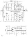
- Fig. 1 presents a motor drive, in which a three-phase alternating-current motor ⁇ 3lM is supplied by two three-phase frequency converters FC1 and FC2 connected to a three-phase network L 1 , L 2 , L 3 , in both of which is an input choke L AC,1 , L AC,2 , a diode rectifier bridge REC11, REC12, a DC-voltage intermediate circuit, in which is a capacitor C 1 , C 2 , and an inverter INU11, INU12 controlled by control pulses obtained from a control unit CU1, CU2 with pulse width modulation, which is a full-wave bridge rectifier provided with a semiconductor switch, such as an IGBT, and diodes connected in parallel with it.
- a three-phase alternating voltage U, V, W which is supplied to the motor, is received as output voltage from the frequency converter.
- Figs. 2 and 3 present current peaks, caused by the non-simultaneity of the rising edge and falling edge of the control pulse, between appliances connected in parallel.
- Fig. 2 presents the output currents of two frequency converters connected in parallel in a case in which the different timing of the rising edge of the control pulse causes a current peak for the time 70 ⁇ s and increases to be clearly greater than the load current.
- Fig. 3 presents the output currents of two frequency converters connected in parallel in a case in which the different timing of the falling edge of the control pulse causes a current peak limited to the value of the load current for the time of approx. 56 ⁇ s.
- Fig. 4 presents the control pulses of two IGBTs connected in parallel, of which the falling edge of one is delayed by ⁇ t . Delaying of the control pulse is implemented such that the duration of the safety time is not exceeded nor is the rising edge of the control pulse of the IGBT firing after the safety time affected.
- the safety time means the dwell time of the control pulses needed in conjunction with switching of the phase switch, with which simultaneous conduction of the power switches of the upper arm and the lower arm is prevented.
- Fig. 4a is similar to Fig. 4, however with the difference that in this case the safety time also is deferred by the amount ⁇ t , in which case also the rising edge of the control pulse of the IGBT firing after the safety time is delayed by the same amount ⁇ t .
- the main purpose of increasing the inductance is, however, to slow down the smoothing of the current peak caused by non-simultaneous timing. As a result of slower smoothing of the currents, a disbalance occurs in the current distribution of the appliances connected in parallel.
- the magnitude of the disbalance produced can be regulated with a switching time difference of the length ⁇ t .
- the switching time difference implemented for specific phases must also be proportioned to the value of the phase current so that the waveform of the current remains as sinusoidal as possible.
- ⁇ t was, depending on the case, kept constant irrespective of the value of the phase current.
- the switching frequency also affects the minimum requirement for inductance because as the switching frequency decreases, the time interval of non-simultaneous switchings increases. During this time interval the currents equalize at a time constant set by the system. By increasing the inductance the time constant can be increased.
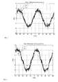
- Figs. 7-8 present the measured output currents of two frequency converters connected in parallel when the power balance is regulated by means of the falling edge of the control pulse and inductances of 200 ⁇ H are connected between the output terminals and the common points (i.e. 400 ⁇ H inductance between the output terminals).
- the disbalance caused to current distribution by the delay of the falling edge can be clearly seen in the measurement figures 7 - 8.
- the distortion of the waveform of the current caused by the unscaled delay to the current can also be clearly seen in Fig. 8.
- By delaying the falling edge of the control pulse it is thus possible to regulate, among other things, the disbalance caused by non-idealities of the output stages.
- the current distribution is shown in Fig. 6. The distribution seems to be almost directly comparable to the length of the delay. The above holds true, however, only in cases in which there is sufficient inductance between the output terminals.
Abstract
Description
- The present invention relates to a method for balancing the output powers of frequency converters connected in parallel. The invention also relates to a parallel connection arrangement of power converter units connected in parallel.
- Parallel connection of frequency converters is required in the control of motors of very high output power (e.g. > 1 MW), because owing to the power components available the power handling ability of individual frequency converters is substantially smaller.
- The distribution of power between appliances connected in parallel is not generally uniform, even if the switching instructions are simultaneous. Uneven distribution causes, among other things, non-idealities of power modules and non-simultaneities of control pulses caused by the control circuits. Fig. 1 presents a parallel connection formed from two frequency converters. In the parallel connection presented in the figure, the non-simultaneities of the control pulses cause current peaks between the appliances; in the worst case, a short-circuit between the appliances. The non-simultaneity of the control pulses corresponds in principle to disparities occurring in the firing delays and extinguishing delays of the power modules.
- Two cases of non-simultaneities of the control pulses must be distinguished; rising-edge non-simultaneity (commutation from the diodes to the IGBT) and falling-edge non-simultaneity (commutation from the IGBT to the diodes). In rising-edge non-simultaneity the IGBTs of the parallel appliances are fired at different times. The IGBT fired first takes the greatest part of the load current. When the switching time difference is sufficient, the current peak can grow to be greater than the load current. In falling-edge non-simultaneity the IGBTs are extinguished at different times. Now the IGBT extinguished last takes the greatest part of the load current. The current peak produced can in this case grow to the same magnitude as the load current.
- The firing controls of the power switches according to this invention are simultaneous and the power balance regulation is implemented simply by changing the timing of the falling edge of the control pulse such that the falling edge of the control pulse of the IGBT conducting the current is delayed.
- The characteristic features of the solution according to the invention are described in detail in the claims below.
- In the following, the invention will be described in more detail by the aid of an embodiment with reference to the attached drawings, wherein
- Fig. 1 presents two frequency converters connected in parallel, which supply an alternating-current electric motor.
- Fig. 2 presents the output currents of frequency converters connected in parallel, in the case where the rising edges of the control pulses are not simultaneous.
- Fig. 3 presents the output currents of frequency converters connected in parallel, in the case where the falling edges of the control pulses are not simultaneous.
- Fig. 4 presents the control pulses of two IGBTs connected in parallel, of which the falling edge of one is delayed by Δt at the expense of the safety time.
- Fig. 4a presents the control pulses of two IGBTs connected in parallel, of which the falling edge of one is delayed by Δt without shortening the safety time.
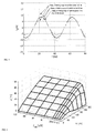
- Fig. 5 presents the simulated output currents of frequency converters connected in parallel when the delay of the falling edge of the control pulse is varied between Δt=0...100 ns, the inductance between the output terminals and the common point L out=100 µH and the switching frequency is 10 kHz.
- Fig. 6 presents the disbalance d of the effective values of frequency converters connected in parallel as a function of the inductance Lout between the output terminals and the common point and of the delay Δt of the falling edge of the control pulse.
- Figs. 7 and 8 present the measured output currents of frequency converters connected in parallel when the delay of the falling edge of the control pulse Δt=0 ns and Δt=300 ns, the inductance between the output terminals and the common point L out=200 µH and the switching frequency is 10 kHz.
- Fig. 1 presents a motor drive, in which a three-phase alternating-current motor ~3lM is supplied by two three-phase frequency converters FC1 and FC2 connected to a three-phase network L1, L2, L3, in both of which is an input choke LAC,1, LAC,2, a diode rectifier bridge REC11, REC12, a DC-voltage intermediate circuit, in which is a capacitor C1, C2, and an inverter INU11, INU12 controlled by control pulses obtained from a control unit CU1, CU2 with pulse width modulation, which is a full-wave bridge rectifier provided with a semiconductor switch, such as an IGBT, and diodes connected in parallel with it. A three-phase alternating voltage U, V, W, which is supplied to the motor, is received as output voltage from the frequency converter.
- Figs. 2 and 3 present current peaks, caused by the non-simultaneity of the rising edge and falling edge of the control pulse, between appliances connected in parallel. Fig. 2 presents the output currents of two frequency converters connected in parallel in a case in which the different timing of the rising edge of the control pulse causes a current peak for the
time 70 µs and increases to be clearly greater than the load current. Fig. 3 presents the output currents of two frequency converters connected in parallel in a case in which the different timing of the falling edge of the control pulse causes a current peak limited to the value of the load current for the time of approx. 56 µs. - Fig. 4 presents the control pulses of two IGBTs connected in parallel, of which the falling edge of one is delayed by Δt. Delaying of the control pulse is implemented such that the duration of the safety time is not exceeded nor is the rising edge of the control pulse of the IGBT firing after the safety time affected. The safety time means the dwell time of the control pulses needed in conjunction with switching of the phase switch, with which simultaneous conduction of the power switches of the upper arm and the lower arm is prevented. When the time differences made in the falling edge of the control pulses are small and inductance is added between the output terminals of the appliances connected in parallel, the amplitudes of current peaks caused by non-simultaneous control pulses do not grow substantially. This is important because with non-simultaneity of the falling edge the IGBT that extinguishes last conducts a large part of the load current and the current peak can grow to be as great as the load current. In this case it is necessary to cut off substantial overcurrent from the IGBT that extinguishes last, in which case the voltage stress over the power switch grows.
- Fig. 4a is similar to Fig. 4, however with the difference that in this case the safety time also is deferred by the amount Δt, in which case also the rising edge of the control pulse of the IGBT firing after the safety time is delayed by the same amount Δt.
- The main purpose of increasing the inductance is, however, to slow down the smoothing of the current peak caused by non-simultaneous timing. As a result of slower smoothing of the currents, a disbalance occurs in the current distribution of the appliances connected in parallel. The magnitude of the disbalance produced can be regulated with a switching time difference of the length Δt. The switching time difference implemented for specific phases must also be proportioned to the value of the phase current so that the waveform of the current remains as sinusoidal as possible.
- Fig. 5 presents the output currents of frequency converters connected in parallel when the delay of the falling edge of the control pulse is varied between Δt=0...100 ns. Δt was, depending on the case, kept constant irrespective of the value of the phase current. The inductance between the output terminals and the common point was 100 µH (
i.e. inductance 200 µH between the input terminals). It can be seen from the figure that the delay implemented in the falling edge of the control pulse causes a distinct disbalance in the current distribution. - Fig. 6 presents the disbalance d of the effective values of the output currents when the delay of the falling edge of the control pulse is varied between Δt=0...300 ns and the inductance between the output terminal and the common point varied between 1...100 µH (i.e. inductance between the output terminals varied between 2... 200 µH). Δt was, depending on the case, kept constant irrespective of the value of the phase current. The disbalance in the effective values is solved with the equation

the solution of which gives the difference of the current of the most loaded appliance with respect to the average value of the currents. It can be clearly seen from the figure that the delay implemented in the falling edge of the control pulse is not able to cause disbalance between the appliances connected in parallel if the inductance between the output terminals and the common point is too small (e.g. only short cables between the output terminals). The maximum permitted current deviation Δ/max, the switching frequency f sw and the maximum permitted delay of the falling edge Δt affect the measurement of inductance. One minimum requirement for inductance is obtained with the equation
where ΔU is the voltage difference between the output terminals during the switching time difference. The switching frequency also affects the minimum requirement for inductance because as the switching frequency decreases, the time interval of non-simultaneous switchings increases. During this time interval the currents equalize at a time constant set by the system. By increasing the inductance the time constant can be increased. - Figs. 7-8 present the measured output currents of two frequency converters connected in parallel when the power balance is regulated by means of the falling edge of the control pulse and inductances of 200 µH are connected between the output terminals and the common points (i.e. 400 µH inductance between the output terminals). In the examples of the figures the delay of the falling edge of the control pulses Δt=0 and Δt=300 ns, and it remains constant irrespective of the value of the phase current. In Fig. 7 the control pulses are identical, i.e. Δt=0 ns and in Fig. 8 Δt=300 ns.
- The disbalance caused to current distribution by the delay of the falling edge can be clearly seen in the measurement figures 7 - 8. The distortion of the waveform of the current caused by the unscaled delay to the current can also be clearly seen in Fig. 8. By delaying the falling edge of the control pulse it is thus possible to regulate, among other things, the disbalance caused by non-idealities of the output stages. The current distribution is shown in Fig. 6. The distribution seems to be almost directly comparable to the length of the delay. The above holds true, however, only in cases in which there is sufficient inductance between the output terminals.
- By synchronizing the firing times, the current peak produced between appliances connected in parallel can be eliminated, which can increase the load current to a higher value. When the firing times are synchronized, uneven distribution of the power can be regulated by delaying the falling edge of the control pulse.
- It is obvious to the person skilled in the art that the different embodiments of the invention are not limited solely to the example described above, but that they may be varied within the scope of the claims presented below. Instead of separate control units, the semiconductor switches of the inverters can also be controlled with a shared control unit.
Claims (4)
- A method for equalizing the output powers of power converter units (INU11, INU12), in which power converter units is a semiconductor switch bridge controlled with pulse width modulation, in which control are control pulses with which the semiconductor switches are controlled,
characterized in that in the method the falling edge of the control pulses of at least one semiconductor switch of at least one power converter unit is delayed. - A method according to claim 1, in which the delay of the falling edge of the control pulse changes as a function of the output current.
- A parallel connection arrangement for equalizing the output powers of power converter units (INU11, INU12) connected in parallel,
in which power converter units is a semiconductor switch bridge controlled with pulse width modulation, and
in which is a control unit arrangement (CU1, CU2) for forming control pulses, with which the semiconductor switches are controlled,
characterized in that the control unit arrangement delays the falling edge of the control pulses of at least one semiconductor switch of at least one power converter unit. - A parallel connection arrangement according to claim 3, in which the delay of the falling edge of the control pulse changes as a function of the output current.
Applications Claiming Priority (1)
| Application Number | Priority Date | Filing Date | Title |
|---|---|---|---|
| FI20060759A FI118876B (en) | 2006-08-25 | 2006-08-25 | Power balance in parallel connected drives |
Publications (3)
| Publication Number | Publication Date |
|---|---|
| EP1892822A2 true EP1892822A2 (en) | 2008-02-27 |
| EP1892822A3 EP1892822A3 (en) | 2010-09-22 |
| EP1892822B1 EP1892822B1 (en) | 2022-02-16 |
Family
ID=36950660
Family Applications (1)
| Application Number | Title | Priority Date | Filing Date |
|---|---|---|---|
| EP07075681.2A Active EP1892822B1 (en) | 2006-08-25 | 2007-08-14 | Power level balance of frequency converters connected in parallel |
Country Status (3)
| Country | Link |
|---|---|
| US (1) | US7872885B2 (en) |
| EP (1) | EP1892822B1 (en) |
| FI (1) | FI118876B (en) |
Cited By (3)
| Publication number | Priority date | Publication date | Assignee | Title |
|---|---|---|---|---|
| WO2015090627A1 (en) * | 2013-12-19 | 2015-06-25 | Abb Technology Ltd. | Power unit and multi-phase electric drive using the same |
| CN105576642A (en) * | 2014-11-03 | 2016-05-11 | 通用电气公司 | Systems and methods of monitoring a power system power converter |
| US10707777B2 (en) | 2015-10-09 | 2020-07-07 | Vacon Oy | Control of parallel connected power devices |
Families Citing this family (10)
| Publication number | Priority date | Publication date | Assignee | Title |
|---|---|---|---|---|
| US8730702B2 (en) * | 2009-03-03 | 2014-05-20 | Renewable Power Conversion, Inc. | Very high efficiency three phase power converter |
| DE102010003614A1 (en) * | 2010-04-01 | 2011-10-06 | Robert Bosch Gmbh | Circuit arrangement with at least two parallel-connected inverter modules, method for parallel connection of at least two inverter modules and circuit carrier for a gate drive circuit of an inverter module |
| CN102891612B (en) * | 2012-09-21 | 2014-12-10 | 上海交通大学 | Current non-equalizing control method of converter multi-unit parallel system |
| CN107112928B (en) | 2014-12-17 | 2021-01-15 | 奥的斯电梯公司 | Conveyor system with parallel drives |
| CN104836463B (en) * | 2015-04-30 | 2018-01-05 | 华南理工大学 | Mixing transformation system based on three-phase PWM rectification Yu multiple-unit uncontrollable rectifier |
| CN104883073B (en) * | 2015-06-01 | 2017-08-01 | 南车株洲电力机车研究所有限公司 | Current transformer is flowed in multiple module paralleling output |
| CN107565800B (en) * | 2016-06-30 | 2020-05-15 | 西门子公司 | Gate driving circuit and gate driving method |
| EP3574579B1 (en) | 2017-01-30 | 2023-11-08 | Carrier Corporation | Paralleled passive front-end rectifiers with and without interleaving |
| EP3574580B1 (en) | 2017-01-30 | 2024-02-28 | Carrier Corporation | Method of controlling paralleled passive front-end rectifiers |
| CN109361324B (en) * | 2018-12-24 | 2020-10-13 | 中国船舶重工集团公司第七一九研究所 | Three-phase inverter power supply parallel power balancing method based on zero sequence component |
Citations (6)
| Publication number | Priority date | Publication date | Assignee | Title |
|---|---|---|---|---|
| DE4038869C1 (en) | 1990-12-01 | 1991-08-01 | Licentia Patent-Verwaltungs-Gmbh, 6000 Frankfurt, De | Current symmetrising circuitry for parallel converters - having branches of semiconductor switches and phase outputs coupled together via choke coils |
| EP0524398A2 (en) | 1991-07-23 | 1993-01-27 | Kabushiki Kaisha Meidensha | Circuit for controlling output current balance between parallel driven PWM-type power inverting units |
| EP0600312A2 (en) | 1992-12-03 | 1994-06-08 | Inventio Ag | Method of controlling parallel-connected inverters on the basis of current maximal values |
| DE4341868A1 (en) | 1992-12-09 | 1994-06-23 | Mitsubishi Electric Corp | Parallel dual inverter circuit with high power capability |
| US5757634A (en) | 1996-12-24 | 1998-05-26 | Siemans Electric Limited | Multiparalleling system of voltage source power converters |
| EP1427094A2 (en) | 2002-12-06 | 2004-06-09 | Loher GmbH | Method for operating several pulse controlled inverters connected in parallel |
Family Cites Families (8)
| Publication number | Priority date | Publication date | Assignee | Title |
|---|---|---|---|---|
| ZA837849B (en) * | 1982-11-03 | 1984-06-27 | Bbc Brown Boveri & Cie | Static power converter |
| US4849870A (en) * | 1988-01-25 | 1989-07-18 | Westinghouse Electric Corp. | Method of operating a-c drive with parallel connected d-c link power converters |
| US5272612A (en) * | 1989-06-30 | 1993-12-21 | Kabushiki Kaisha Toshiba | X-ray power supply utilizing A.C. frequency conversion to generate a high D.C. voltage |
| ATE137365T1 (en) | 1990-11-19 | 1996-05-15 | Inventio Ag | METHOD AND DEVICE FOR CONNECTING INVERTERS IN PARALLEL |
| US5923550A (en) * | 1996-05-01 | 1999-07-13 | General Electric Company | Interference reduction by harmonic phase shift in multiple PWM rectifier operation |
| EP1575156B1 (en) * | 2004-02-16 | 2015-06-17 | Vacon Oyj | Synchronization of parallel-connected inverter units or frequency converters |
| JP4967584B2 (en) * | 2006-10-12 | 2012-07-04 | トヨタ自動車株式会社 | Converter control device |
| US7852643B2 (en) * | 2007-06-27 | 2010-12-14 | General Electric Company | Cross current control for power converter system |
-
2006
- 2006-08-25 FI FI20060759A patent/FI118876B/en active IP Right Grant
-
2007
- 2007-08-14 EP EP07075681.2A patent/EP1892822B1/en active Active
- 2007-08-20 US US11/892,110 patent/US7872885B2/en active Active
Patent Citations (6)
| Publication number | Priority date | Publication date | Assignee | Title |
|---|---|---|---|---|
| DE4038869C1 (en) | 1990-12-01 | 1991-08-01 | Licentia Patent-Verwaltungs-Gmbh, 6000 Frankfurt, De | Current symmetrising circuitry for parallel converters - having branches of semiconductor switches and phase outputs coupled together via choke coils |
| EP0524398A2 (en) | 1991-07-23 | 1993-01-27 | Kabushiki Kaisha Meidensha | Circuit for controlling output current balance between parallel driven PWM-type power inverting units |
| EP0600312A2 (en) | 1992-12-03 | 1994-06-08 | Inventio Ag | Method of controlling parallel-connected inverters on the basis of current maximal values |
| DE4341868A1 (en) | 1992-12-09 | 1994-06-23 | Mitsubishi Electric Corp | Parallel dual inverter circuit with high power capability |
| US5757634A (en) | 1996-12-24 | 1998-05-26 | Siemans Electric Limited | Multiparalleling system of voltage source power converters |
| EP1427094A2 (en) | 2002-12-06 | 2004-06-09 | Loher GmbH | Method for operating several pulse controlled inverters connected in parallel |
Cited By (3)
| Publication number | Priority date | Publication date | Assignee | Title |
|---|---|---|---|---|
| WO2015090627A1 (en) * | 2013-12-19 | 2015-06-25 | Abb Technology Ltd. | Power unit and multi-phase electric drive using the same |
| CN105576642A (en) * | 2014-11-03 | 2016-05-11 | 通用电气公司 | Systems and methods of monitoring a power system power converter |
| US10707777B2 (en) | 2015-10-09 | 2020-07-07 | Vacon Oy | Control of parallel connected power devices |
Also Published As
| Publication number | Publication date |
|---|---|
| FI20060759A (en) | 2008-02-26 |
| EP1892822A3 (en) | 2010-09-22 |
| US7872885B2 (en) | 2011-01-18 |
| FI20060759A0 (en) | 2006-08-25 |
| FI118876B (en) | 2008-04-15 |
| US20080049462A1 (en) | 2008-02-28 |
| EP1892822B1 (en) | 2022-02-16 |
Similar Documents
| Publication | Publication Date | Title |
|---|---|---|
| EP1892822A2 (en) | Power level balance of frequency converters connected in parallel | |
| EP3657661B1 (en) | Conversion circuit, control method, and power supply device | |
| EP2475088B1 (en) | Pulse width modulation control method and system for mitigating reflected wave effects in over-modulation region | |
| EP3068023B1 (en) | Inrush limiter for motor drive ac/ac power converters | |
| EP1175814A2 (en) | Resonant frequency induction furnace system using capacitive voltage division | |
| US10707777B2 (en) | Control of parallel connected power devices | |
| US20050207194A1 (en) | Control device and process of a converter and converter and electrical installation comprising such a device | |
| EP4167432A1 (en) | Power supply circuit without charging loop, and power management system | |
| EP0697764B1 (en) | Voltage, phase and frequency control by miniature inverter system | |
| EP3062413A1 (en) | Voltage source converter and control thereof | |
| EP2940846B1 (en) | A method of initiating a regenerative converter and a regenerative converter | |
| US11381158B2 (en) | Method for controlling a power converter in a fault condition state and protection of same | |
| EP0272776A2 (en) | Three-phase supply system | |
| EP2011225B1 (en) | Motor control | |
| EP2911287A1 (en) | Apparatus and method for reducing harmonics | |
| EP3571757B1 (en) | Energy reset of a modular multilevel converter | |
| KR101793062B1 (en) | NPC Converting Device and Method | |
| KR102269005B1 (en) | Generator system | |
| CN109874388B (en) | Method for operating an inverter and inverter | |
| Salim | Phase Conversion of VFD based Induction Motor | |
| KR102099975B1 (en) | Parallel rectifier capable of reducing ripples by controlling current | |
| WO2012116426A1 (en) | High power ac to dc conversion | |
| CN115004534B (en) | Three-level inverter, control method and system | |
| DK178199B1 (en) | Method for controlling the shape of the rising and falling edges of an output voltage pulse of a PWM converter | |
| KR20160116657A (en) | Control method for an ac motor using the reverse-phase control method, and the implemented system thereof |
Legal Events
| Date | Code | Title | Description |
|---|---|---|---|
| PUAI | Public reference made under article 153(3) epc to a published international application that has entered the european phase |
Free format text: ORIGINAL CODE: 0009012 |
|
| AK | Designated contracting states |
Kind code of ref document: A2 Designated state(s): AT BE BG CH CY CZ DE DK EE ES FI FR GB GR HU IE IS IT LI LT LU LV MC MT NL PL PT RO SE SI SK TR |
|
| AX | Request for extension of the european patent |
Extension state: AL BA HR MK YU |
|
| PUAL | Search report despatched |
Free format text: ORIGINAL CODE: 0009013 |
|
| AK | Designated contracting states |
Kind code of ref document: A3 Designated state(s): AT BE BG CH CY CZ DE DK EE ES FI FR GB GR HU IE IS IT LI LT LU LV MC MT NL PL PT RO SE SI SK TR |
|
| AX | Request for extension of the european patent |
Extension state: AL BA HR MK RS |
|
| RIC1 | Information provided on ipc code assigned before grant |
Ipc: H03K 17/687 20060101ALI20100813BHEP Ipc: H03K 17/12 20060101ALI20100813BHEP Ipc: H03K 17/0812 20060101ALI20100813BHEP Ipc: H02M 1/088 20060101ALI20100813BHEP Ipc: H02M 7/493 20070101ALI20100813BHEP Ipc: H02M 5/458 20060101AFI20071205BHEP |
|
| 17P | Request for examination filed |
Effective date: 20110321 |
|
| AKY | No designation fees paid | ||
| RBV | Designated contracting states (corrected) |
Designated state(s): AT BE BG CH CY CZ DE DK EE ES FI FR GB GR HU IE IS IT LI LT LU LV MC MT NL PL PT RO SE SI SK TR |
|
| REG | Reference to a national code |
Ref country code: DE Ref legal event code: R108 Effective date: 20110426 |
|
| 17Q | First examination report despatched |
Effective date: 20120410 |
|
| STAA | Information on the status of an ep patent application or granted ep patent |
Free format text: STATUS: EXAMINATION IS IN PROGRESS |
|
| RAP1 | Party data changed (applicant data changed or rights of an application transferred) |
Owner name: VACON OY |
|
| APBK | Appeal reference recorded |
Free format text: ORIGINAL CODE: EPIDOSNREFNE |
|
| APBN | Date of receipt of notice of appeal recorded |
Free format text: ORIGINAL CODE: EPIDOSNNOA2E |
|
| APBR | Date of receipt of statement of grounds of appeal recorded |
Free format text: ORIGINAL CODE: EPIDOSNNOA3E |
|
| APAF | Appeal reference modified |
Free format text: ORIGINAL CODE: EPIDOSCREFNE |
|
| APBT | Appeal procedure closed |
Free format text: ORIGINAL CODE: EPIDOSNNOA9E |
|
| GRAP | Despatch of communication of intention to grant a patent |
Free format text: ORIGINAL CODE: EPIDOSNIGR1 |
|
| STAA | Information on the status of an ep patent application or granted ep patent |
Free format text: STATUS: GRANT OF PATENT IS INTENDED |
|
| INTG | Intention to grant announced |
Effective date: 20210927 |
|
| GRAS | Grant fee paid |
Free format text: ORIGINAL CODE: EPIDOSNIGR3 |
|
| GRAA | (expected) grant |
Free format text: ORIGINAL CODE: 0009210 |
|
| STAA | Information on the status of an ep patent application or granted ep patent |
Free format text: STATUS: THE PATENT HAS BEEN GRANTED |
|
| AK | Designated contracting states |
Kind code of ref document: B1 Designated state(s): AT BE BG CH CY CZ DE DK EE ES FI FR GB GR HU IE IS IT LI LT LU LV MC MT NL PL PT RO SE SI SK TR |
|
| REG | Reference to a national code |
Ref country code: GB Ref legal event code: FG4D |
|
| REG | Reference to a national code |
Ref country code: CH Ref legal event code: EP |
|
| REG | Reference to a national code |
Ref country code: DE Ref legal event code: R096 Ref document number: 602007061432 Country of ref document: DE |
|
| REG | Reference to a national code |
Ref country code: AT Ref legal event code: REF Ref document number: 1469508 Country of ref document: AT Kind code of ref document: T Effective date: 20220315 |
|
| REG | Reference to a national code |
Ref country code: IE Ref legal event code: FG4D |
|
| REG | Reference to a national code |
Ref country code: LT Ref legal event code: MG9D |
|
| REG | Reference to a national code |
Ref country code: NL Ref legal event code: MP Effective date: 20220216 |
|
| REG | Reference to a national code |
Ref country code: AT Ref legal event code: MK05 Ref document number: 1469508 Country of ref document: AT Kind code of ref document: T Effective date: 20220216 |
|
| PG25 | Lapsed in a contracting state [announced via postgrant information from national office to epo] |
Ref country code: SE Free format text: LAPSE BECAUSE OF FAILURE TO SUBMIT A TRANSLATION OF THE DESCRIPTION OR TO PAY THE FEE WITHIN THE PRESCRIBED TIME-LIMIT Effective date: 20220216 Ref country code: PT Free format text: LAPSE BECAUSE OF FAILURE TO SUBMIT A TRANSLATION OF THE DESCRIPTION OR TO PAY THE FEE WITHIN THE PRESCRIBED TIME-LIMIT Effective date: 20220616 Ref country code: NL Free format text: LAPSE BECAUSE OF FAILURE TO SUBMIT A TRANSLATION OF THE DESCRIPTION OR TO PAY THE FEE WITHIN THE PRESCRIBED TIME-LIMIT Effective date: 20220216 Ref country code: LT Free format text: LAPSE BECAUSE OF FAILURE TO SUBMIT A TRANSLATION OF THE DESCRIPTION OR TO PAY THE FEE WITHIN THE PRESCRIBED TIME-LIMIT Effective date: 20220216 Ref country code: ES Free format text: LAPSE BECAUSE OF FAILURE TO SUBMIT A TRANSLATION OF THE DESCRIPTION OR TO PAY THE FEE WITHIN THE PRESCRIBED TIME-LIMIT Effective date: 20220216 Ref country code: BG Free format text: LAPSE BECAUSE OF FAILURE TO SUBMIT A TRANSLATION OF THE DESCRIPTION OR TO PAY THE FEE WITHIN THE PRESCRIBED TIME-LIMIT Effective date: 20220516 |
|
| PG25 | Lapsed in a contracting state [announced via postgrant information from national office to epo] |
Ref country code: PL Free format text: LAPSE BECAUSE OF FAILURE TO SUBMIT A TRANSLATION OF THE DESCRIPTION OR TO PAY THE FEE WITHIN THE PRESCRIBED TIME-LIMIT Effective date: 20220216 Ref country code: LV Free format text: LAPSE BECAUSE OF FAILURE TO SUBMIT A TRANSLATION OF THE DESCRIPTION OR TO PAY THE FEE WITHIN THE PRESCRIBED TIME-LIMIT Effective date: 20220216 Ref country code: GR Free format text: LAPSE BECAUSE OF FAILURE TO SUBMIT A TRANSLATION OF THE DESCRIPTION OR TO PAY THE FEE WITHIN THE PRESCRIBED TIME-LIMIT Effective date: 20220517 Ref country code: FI Free format text: LAPSE BECAUSE OF FAILURE TO SUBMIT A TRANSLATION OF THE DESCRIPTION OR TO PAY THE FEE WITHIN THE PRESCRIBED TIME-LIMIT Effective date: 20220216 Ref country code: AT Free format text: LAPSE BECAUSE OF FAILURE TO SUBMIT A TRANSLATION OF THE DESCRIPTION OR TO PAY THE FEE WITHIN THE PRESCRIBED TIME-LIMIT Effective date: 20220216 |
|
| PG25 | Lapsed in a contracting state [announced via postgrant information from national office to epo] |
Ref country code: IS Free format text: LAPSE BECAUSE OF FAILURE TO SUBMIT A TRANSLATION OF THE DESCRIPTION OR TO PAY THE FEE WITHIN THE PRESCRIBED TIME-LIMIT Effective date: 20220616 |
|
| PG25 | Lapsed in a contracting state [announced via postgrant information from national office to epo] |
Ref country code: SK Free format text: LAPSE BECAUSE OF FAILURE TO SUBMIT A TRANSLATION OF THE DESCRIPTION OR TO PAY THE FEE WITHIN THE PRESCRIBED TIME-LIMIT Effective date: 20220216 Ref country code: RO Free format text: LAPSE BECAUSE OF FAILURE TO SUBMIT A TRANSLATION OF THE DESCRIPTION OR TO PAY THE FEE WITHIN THE PRESCRIBED TIME-LIMIT Effective date: 20220216 Ref country code: EE Free format text: LAPSE BECAUSE OF FAILURE TO SUBMIT A TRANSLATION OF THE DESCRIPTION OR TO PAY THE FEE WITHIN THE PRESCRIBED TIME-LIMIT Effective date: 20220216 Ref country code: DK Free format text: LAPSE BECAUSE OF FAILURE TO SUBMIT A TRANSLATION OF THE DESCRIPTION OR TO PAY THE FEE WITHIN THE PRESCRIBED TIME-LIMIT Effective date: 20220216 Ref country code: CZ Free format text: LAPSE BECAUSE OF FAILURE TO SUBMIT A TRANSLATION OF THE DESCRIPTION OR TO PAY THE FEE WITHIN THE PRESCRIBED TIME-LIMIT Effective date: 20220216 |
|
| REG | Reference to a national code |
Ref country code: DE Ref legal event code: R097 Ref document number: 602007061432 Country of ref document: DE |
|
| PLBE | No opposition filed within time limit |
Free format text: ORIGINAL CODE: 0009261 |
|
| STAA | Information on the status of an ep patent application or granted ep patent |
Free format text: STATUS: NO OPPOSITION FILED WITHIN TIME LIMIT |
|
| 26N | No opposition filed |
Effective date: 20221117 |
|
| PG25 | Lapsed in a contracting state [announced via postgrant information from national office to epo] |
Ref country code: SI Free format text: LAPSE BECAUSE OF FAILURE TO SUBMIT A TRANSLATION OF THE DESCRIPTION OR TO PAY THE FEE WITHIN THE PRESCRIBED TIME-LIMIT Effective date: 20220216 |
|
| PG25 | Lapsed in a contracting state [announced via postgrant information from national office to epo] |
Ref country code: MC Free format text: LAPSE BECAUSE OF FAILURE TO SUBMIT A TRANSLATION OF THE DESCRIPTION OR TO PAY THE FEE WITHIN THE PRESCRIBED TIME-LIMIT Effective date: 20220216 |
|
| REG | Reference to a national code |
Ref country code: CH Ref legal event code: PL |
|
| GBPC | Gb: european patent ceased through non-payment of renewal fee |
Effective date: 20220814 |
|
| PG25 | Lapsed in a contracting state [announced via postgrant information from national office to epo] |
Ref country code: LU Free format text: LAPSE BECAUSE OF NON-PAYMENT OF DUE FEES Effective date: 20220814 Ref country code: LI Free format text: LAPSE BECAUSE OF NON-PAYMENT OF DUE FEES Effective date: 20220831 Ref country code: CH Free format text: LAPSE BECAUSE OF NON-PAYMENT OF DUE FEES Effective date: 20220831 |
|
| REG | Reference to a national code |
Ref country code: BE Ref legal event code: MM Effective date: 20220831 |
|
| P01 | Opt-out of the competence of the unified patent court (upc) registered |
Effective date: 20230621 |
|
| PG25 | Lapsed in a contracting state [announced via postgrant information from national office to epo] |
Ref country code: IT Free format text: LAPSE BECAUSE OF FAILURE TO SUBMIT A TRANSLATION OF THE DESCRIPTION OR TO PAY THE FEE WITHIN THE PRESCRIBED TIME-LIMIT Effective date: 20220216 Ref country code: IE Free format text: LAPSE BECAUSE OF NON-PAYMENT OF DUE FEES Effective date: 20220814 Ref country code: FR Free format text: LAPSE BECAUSE OF NON-PAYMENT OF DUE FEES Effective date: 20220831 |
|
| PG25 | Lapsed in a contracting state [announced via postgrant information from national office to epo] |
Ref country code: BE Free format text: LAPSE BECAUSE OF NON-PAYMENT OF DUE FEES Effective date: 20220831 |
|
| PG25 | Lapsed in a contracting state [announced via postgrant information from national office to epo] |
Ref country code: GB Free format text: LAPSE BECAUSE OF NON-PAYMENT OF DUE FEES Effective date: 20220814 |
|
| PGFP | Annual fee paid to national office [announced via postgrant information from national office to epo] |
Ref country code: DE Payment date: 20230705 Year of fee payment: 17 |
|
| PG25 | Lapsed in a contracting state [announced via postgrant information from national office to epo] |
Ref country code: HU Free format text: LAPSE BECAUSE OF FAILURE TO SUBMIT A TRANSLATION OF THE DESCRIPTION OR TO PAY THE FEE WITHIN THE PRESCRIBED TIME-LIMIT; INVALID AB INITIO Effective date: 20070814 |