EP1835324A1 - Mirror device, mirror array, optical switch, mirror device manufacturing method and mirror substrate manufacturing method - Google Patents
Mirror device, mirror array, optical switch, mirror device manufacturing method and mirror substrate manufacturing method Download PDFInfo
- Publication number
- EP1835324A1 EP1835324A1 EP05822402A EP05822402A EP1835324A1 EP 1835324 A1 EP1835324 A1 EP 1835324A1 EP 05822402 A EP05822402 A EP 05822402A EP 05822402 A EP05822402 A EP 05822402A EP 1835324 A1 EP1835324 A1 EP 1835324A1
- Authority
- EP
- European Patent Office
- Prior art keywords
- mirror
- substrate
- electrode
- mirror device
- driving
- Prior art date
- Legal status (The legal status is an assumption and is not a legal conclusion. Google has not performed a legal analysis and makes no representation as to the accuracy of the status listed.)
- Withdrawn
Links
- 239000000758 substrate Substances 0.000 title claims abstract description 673
- 238000004519 manufacturing process Methods 0.000 title claims description 75
- 230000003287 optical effect Effects 0.000 title claims description 74
- 239000010410 layer Substances 0.000 claims description 429
- 229910052751 metal Inorganic materials 0.000 claims description 155
- 239000002184 metal Substances 0.000 claims description 155
- XUIMIQQOPSSXEZ-UHFFFAOYSA-N Silicon Chemical compound [Si] XUIMIQQOPSSXEZ-UHFFFAOYSA-N 0.000 claims description 83
- 229910052710 silicon Inorganic materials 0.000 claims description 83
- 239000010703 silicon Substances 0.000 claims description 83
- 238000005530 etching Methods 0.000 claims description 53
- 230000015572 biosynthetic process Effects 0.000 claims description 40
- 230000005484 gravity Effects 0.000 claims description 39
- 230000033001 locomotion Effects 0.000 claims description 24
- 230000001133 acceleration Effects 0.000 claims description 16
- 239000000463 material Substances 0.000 claims description 15
- 239000011241 protective layer Substances 0.000 claims description 14
- 238000000137 annealing Methods 0.000 claims description 5
- 238000000059 patterning Methods 0.000 claims description 5
- 238000003860 storage Methods 0.000 claims description 5
- 239000011810 insulating material Substances 0.000 claims 2
- 239000007769 metal material Substances 0.000 claims 1
- 239000002585 base Substances 0.000 description 151
- 239000002344 surface layer Substances 0.000 description 110
- 238000003491 array Methods 0.000 description 48
- 229910021421 monocrystalline silicon Inorganic materials 0.000 description 46
- 238000000034 method Methods 0.000 description 41
- 239000000470 constituent Substances 0.000 description 34
- 239000010931 gold Substances 0.000 description 31
- 239000013307 optical fiber Substances 0.000 description 26
- 230000007423 decrease Effects 0.000 description 25
- 238000006073 displacement reaction Methods 0.000 description 25
- 230000008569 process Effects 0.000 description 25
- VYPSYNLAJGMNEJ-UHFFFAOYSA-N Silicium dioxide Chemical compound O=[Si]=O VYPSYNLAJGMNEJ-UHFFFAOYSA-N 0.000 description 24
- KWYUFKZDYYNOTN-UHFFFAOYSA-M Potassium hydroxide Chemical compound [OH-].[K+] KWYUFKZDYYNOTN-UHFFFAOYSA-M 0.000 description 20
- 238000000206 photolithography Methods 0.000 description 20
- 229910052814 silicon oxide Inorganic materials 0.000 description 20
- 239000011159 matrix material Substances 0.000 description 16
- 238000007740 vapor deposition Methods 0.000 description 15
- KRHYYFGTRYWZRS-UHFFFAOYSA-N Fluorane Chemical compound F KRHYYFGTRYWZRS-UHFFFAOYSA-N 0.000 description 14
- PCHJSUWPFVWCPO-UHFFFAOYSA-N gold Chemical compound [Au] PCHJSUWPFVWCPO-UHFFFAOYSA-N 0.000 description 14
- 229910052737 gold Inorganic materials 0.000 description 14
- 238000013459 approach Methods 0.000 description 13
- 238000001312 dry etching Methods 0.000 description 13
- 230000008859 change Effects 0.000 description 12
- 238000001020 plasma etching Methods 0.000 description 12
- 230000000694 effects Effects 0.000 description 11
- 230000005684 electric field Effects 0.000 description 11
- 229920002120 photoresistant polymer Polymers 0.000 description 11
- 238000005259 measurement Methods 0.000 description 10
- 230000004044 response Effects 0.000 description 9
- 238000012546 transfer Methods 0.000 description 9
- 238000001039 wet etching Methods 0.000 description 9
- 238000004380 ashing Methods 0.000 description 8
- 239000012212 insulator Substances 0.000 description 8
- 230000002441 reversible effect Effects 0.000 description 8
- 238000004544 sputter deposition Methods 0.000 description 8
- VYZAMTAEIAYCRO-UHFFFAOYSA-N Chromium Chemical compound [Cr] VYZAMTAEIAYCRO-UHFFFAOYSA-N 0.000 description 7
- 229910052782 aluminium Inorganic materials 0.000 description 7
- XAGFODPZIPBFFR-UHFFFAOYSA-N aluminium Chemical compound [Al] XAGFODPZIPBFFR-UHFFFAOYSA-N 0.000 description 7
- 229910052804 chromium Inorganic materials 0.000 description 7
- 239000011651 chromium Substances 0.000 description 7
- 238000005304 joining Methods 0.000 description 7
- BQCADISMDOOEFD-UHFFFAOYSA-N Silver Chemical compound [Ag] BQCADISMDOOEFD-UHFFFAOYSA-N 0.000 description 6
- 230000003247 decreasing effect Effects 0.000 description 6
- 230000002950 deficient Effects 0.000 description 6
- 238000012986 modification Methods 0.000 description 6
- 230000004048 modification Effects 0.000 description 6
- 238000004806 packaging method and process Methods 0.000 description 6
- 239000011347 resin Substances 0.000 description 6
- 229920005989 resin Polymers 0.000 description 6
- 229910052709 silver Inorganic materials 0.000 description 6
- 239000004332 silver Substances 0.000 description 6
- 239000012670 alkaline solution Substances 0.000 description 5
- 238000013461 design Methods 0.000 description 5
- 230000001681 protective effect Effects 0.000 description 5
- QVGXLLKOCUKJST-UHFFFAOYSA-N atomic oxygen Chemical compound [O] QVGXLLKOCUKJST-UHFFFAOYSA-N 0.000 description 4
- 239000007789 gas Substances 0.000 description 4
- 239000001301 oxygen Substances 0.000 description 4
- 229910052760 oxygen Inorganic materials 0.000 description 4
- 230000007261 regionalization Effects 0.000 description 4
- 229910052581 Si3N4 Inorganic materials 0.000 description 3
- 238000004458 analytical method Methods 0.000 description 3
- 238000001816 cooling Methods 0.000 description 3
- 238000000151 deposition Methods 0.000 description 3
- 238000005516 engineering process Methods 0.000 description 3
- 239000002245 particle Substances 0.000 description 3
- 230000010287 polarization Effects 0.000 description 3
- HQVNEWCFYHHQES-UHFFFAOYSA-N silicon nitride Chemical compound N12[Si]34N5[Si]62N3[Si]51N64 HQVNEWCFYHHQES-UHFFFAOYSA-N 0.000 description 3
- CBENFWSGALASAD-UHFFFAOYSA-N Ozone Chemical compound [O-][O+]=O CBENFWSGALASAD-UHFFFAOYSA-N 0.000 description 2
- 239000000853 adhesive Substances 0.000 description 2
- 230000001070 adhesive effect Effects 0.000 description 2
- 229910045601 alloy Inorganic materials 0.000 description 2
- 239000000956 alloy Substances 0.000 description 2
- 239000004020 conductor Substances 0.000 description 2
- 239000013078 crystal Substances 0.000 description 2
- 230000008021 deposition Effects 0.000 description 2
- 230000005611 electricity Effects 0.000 description 2
- 238000011049 filling Methods 0.000 description 2
- 239000011521 glass Substances 0.000 description 2
- 238000010438 heat treatment Methods 0.000 description 2
- 238000003780 insertion Methods 0.000 description 2
- 230000037431 insertion Effects 0.000 description 2
- 238000011068 loading method Methods 0.000 description 2
- 150000002739 metals Chemical class 0.000 description 2
- 230000003647 oxidation Effects 0.000 description 2
- 238000007254 oxidation reaction Methods 0.000 description 2
- 230000036961 partial effect Effects 0.000 description 2
- 230000002093 peripheral effect Effects 0.000 description 2
- 238000007747 plating Methods 0.000 description 2
- 230000009467 reduction Effects 0.000 description 2
- 239000000377 silicon dioxide Substances 0.000 description 2
- 229910000679 solder Inorganic materials 0.000 description 2
- 239000000126 substance Substances 0.000 description 2
- 239000002253 acid Substances 0.000 description 1
- 239000003513 alkali Substances 0.000 description 1
- JJWKPURADFRFRB-UHFFFAOYSA-N carbonyl sulfide Chemical compound O=C=S JJWKPURADFRFRB-UHFFFAOYSA-N 0.000 description 1
- 230000015556 catabolic process Effects 0.000 description 1
- 238000004140 cleaning Methods 0.000 description 1
- 229910052681 coesite Inorganic materials 0.000 description 1
- 238000004891 communication Methods 0.000 description 1
- 230000000052 comparative effect Effects 0.000 description 1
- 230000008602 contraction Effects 0.000 description 1
- 229910052906 cristobalite Inorganic materials 0.000 description 1
- 238000010586 diagram Methods 0.000 description 1
- 238000001035 drying Methods 0.000 description 1
- 230000005672 electromagnetic field Effects 0.000 description 1
- 238000009713 electroplating Methods 0.000 description 1
- 230000006872 improvement Effects 0.000 description 1
- 230000002401 inhibitory effect Effects 0.000 description 1
- 150000002500 ions Chemical class 0.000 description 1
- 230000007246 mechanism Effects 0.000 description 1
- 230000007935 neutral effect Effects 0.000 description 1
- 238000005498 polishing Methods 0.000 description 1
- 229910021420 polycrystalline silicon Inorganic materials 0.000 description 1
- 229920005591 polysilicon Polymers 0.000 description 1
- 238000004382 potting Methods 0.000 description 1
- 238000012545 processing Methods 0.000 description 1
- 230000005855 radiation Effects 0.000 description 1
- 239000000243 solution Substances 0.000 description 1
- 238000004528 spin coating Methods 0.000 description 1
- 229910052682 stishovite Inorganic materials 0.000 description 1
- 238000002834 transmittance Methods 0.000 description 1
- 229910052905 tridymite Inorganic materials 0.000 description 1
- XLYOFNOQVPJJNP-UHFFFAOYSA-N water Substances O XLYOFNOQVPJJNP-UHFFFAOYSA-N 0.000 description 1
Images


Classifications
-
- B—PERFORMING OPERATIONS; TRANSPORTING
- B81—MICROSTRUCTURAL TECHNOLOGY
- B81B—MICROSTRUCTURAL DEVICES OR SYSTEMS, e.g. MICROMECHANICAL DEVICES
- B81B3/00—Devices comprising flexible or deformable elements, e.g. comprising elastic tongues or membranes
- B81B3/0035—Constitution or structural means for controlling the movement of the flexible or deformable elements
- B81B3/004—Angular deflection
-
- B—PERFORMING OPERATIONS; TRANSPORTING
- B81—MICROSTRUCTURAL TECHNOLOGY
- B81B—MICROSTRUCTURAL DEVICES OR SYSTEMS, e.g. MICROMECHANICAL DEVICES
- B81B3/00—Devices comprising flexible or deformable elements, e.g. comprising elastic tongues or membranes
- B81B3/0064—Constitution or structural means for improving or controlling the physical properties of a device
- B81B3/0086—Electrical characteristics, e.g. reducing driving voltage, improving resistance to peak voltage
-
- G—PHYSICS
- G02—OPTICS
- G02B—OPTICAL ELEMENTS, SYSTEMS OR APPARATUS
- G02B26/00—Optical devices or arrangements for the control of light using movable or deformable optical elements
- G02B26/08—Optical devices or arrangements for the control of light using movable or deformable optical elements for controlling the direction of light
- G02B26/0816—Optical devices or arrangements for the control of light using movable or deformable optical elements for controlling the direction of light by means of one or more reflecting elements
- G02B26/0833—Optical devices or arrangements for the control of light using movable or deformable optical elements for controlling the direction of light by means of one or more reflecting elements the reflecting element being a micromechanical device, e.g. a MEMS mirror, DMD
- G02B26/0841—Optical devices or arrangements for the control of light using movable or deformable optical elements for controlling the direction of light by means of one or more reflecting elements the reflecting element being a micromechanical device, e.g. a MEMS mirror, DMD the reflecting element being moved or deformed by electrostatic means
-
- G—PHYSICS
- G02—OPTICS
- G02B—OPTICAL ELEMENTS, SYSTEMS OR APPARATUS
- G02B6/00—Light guides; Structural details of arrangements comprising light guides and other optical elements, e.g. couplings
- G02B6/24—Coupling light guides
- G02B6/26—Optical coupling means
- G02B6/35—Optical coupling means having switching means
- G02B6/351—Optical coupling means having switching means involving stationary waveguides with moving interposed optical elements
- G02B6/3512—Optical coupling means having switching means involving stationary waveguides with moving interposed optical elements the optical element being reflective, e.g. mirror
- G02B6/3518—Optical coupling means having switching means involving stationary waveguides with moving interposed optical elements the optical element being reflective, e.g. mirror the reflective optical element being an intrinsic part of a MEMS device, i.e. fabricated together with the MEMS device
-
- B—PERFORMING OPERATIONS; TRANSPORTING
- B81—MICROSTRUCTURAL TECHNOLOGY
- B81B—MICROSTRUCTURAL DEVICES OR SYSTEMS, e.g. MICROMECHANICAL DEVICES
- B81B2201/00—Specific applications of microelectromechanical systems
- B81B2201/04—Optical MEMS
- B81B2201/045—Optical switches
-
- B—PERFORMING OPERATIONS; TRANSPORTING
- B81—MICROSTRUCTURAL TECHNOLOGY
- B81B—MICROSTRUCTURAL DEVICES OR SYSTEMS, e.g. MICROMECHANICAL DEVICES
- B81B2203/00—Basic microelectromechanical structures
- B81B2203/05—Type of movement
- B81B2203/058—Rotation out of a plane parallel to the substrate
-
- G—PHYSICS
- G02—OPTICS
- G02B—OPTICAL ELEMENTS, SYSTEMS OR APPARATUS
- G02B6/00—Light guides; Structural details of arrangements comprising light guides and other optical elements, e.g. couplings
- G02B6/24—Coupling light guides
- G02B6/26—Optical coupling means
- G02B6/35—Optical coupling means having switching means
- G02B6/354—Switching arrangements, i.e. number of input/output ports and interconnection types
- G02B6/3554—3D constellations, i.e. with switching elements and switched beams located in a volume
- G02B6/3556—NxM switch, i.e. regular arrays of switches elements of matrix type constellation
-
- G—PHYSICS
- G02—OPTICS
- G02B—OPTICAL ELEMENTS, SYSTEMS OR APPARATUS
- G02B6/00—Light guides; Structural details of arrangements comprising light guides and other optical elements, e.g. couplings
- G02B6/24—Coupling light guides
- G02B6/26—Optical coupling means
- G02B6/35—Optical coupling means having switching means
- G02B6/3564—Mechanical details of the actuation mechanism associated with the moving element or mounting mechanism details
- G02B6/3584—Mechanical details of the actuation mechanism associated with the moving element or mounting mechanism details constructional details of an associated actuator having a MEMS construction, i.e. constructed using semiconductor technology such as etching
-
- Y—GENERAL TAGGING OF NEW TECHNOLOGICAL DEVELOPMENTS; GENERAL TAGGING OF CROSS-SECTIONAL TECHNOLOGIES SPANNING OVER SEVERAL SECTIONS OF THE IPC; TECHNICAL SUBJECTS COVERED BY FORMER USPC CROSS-REFERENCE ART COLLECTIONS [XRACs] AND DIGESTS
- Y10—TECHNICAL SUBJECTS COVERED BY FORMER USPC
- Y10T—TECHNICAL SUBJECTS COVERED BY FORMER US CLASSIFICATION
- Y10T156/00—Adhesive bonding and miscellaneous chemical manufacture
- Y10T156/10—Methods of surface bonding and/or assembly therefor
-
- Y—GENERAL TAGGING OF NEW TECHNOLOGICAL DEVELOPMENTS; GENERAL TAGGING OF CROSS-SECTIONAL TECHNOLOGIES SPANNING OVER SEVERAL SECTIONS OF THE IPC; TECHNICAL SUBJECTS COVERED BY FORMER USPC CROSS-REFERENCE ART COLLECTIONS [XRACs] AND DIGESTS
- Y10—TECHNICAL SUBJECTS COVERED BY FORMER USPC
- Y10T—TECHNICAL SUBJECTS COVERED BY FORMER US CLASSIFICATION
- Y10T29/00—Metal working
- Y10T29/49—Method of mechanical manufacture
- Y10T29/49826—Assembling or joining
- Y10T29/49885—Assembling or joining with coating before or during assembling
Definitions
- the present invention relates to an electrostatically driven mirror device having a mirror with changeable tilt angles, a mirror array having a plurality of mirror devices arranged two-dimensionally, an optical switch having the mirror array, a method of manufacturing the mirror device, and a method of manufacturing a mirror substrate included in the mirror device.
- MEMS optical switches have received a great deal of attention as a hardware technology to implement large-scale optical switches.
- the most characteristic component of a MEMS optical switch is a MEMS mirror array.
- the MEMS mirror array includes a plurality of MEMS mirror devices (to be referred to as mirror devices hereinafter) arrayed two-dimensionally.
- a conventional mirror device see, e.g., Japanese Patent No. 3579015 ) will be described below.
- an insulating layer 8002 made of a silicon oxide film is formed on a lower substrate 8001 of single-crystal silicon.
- Four driving electrodes 8003-1 to 8003-4 are provided on the insulating layer 8002 at the center of the substrate 8001.
- Supports 8004 of single-crystal silicon are provided on both sides of the upper surface of the lower substrate 8001.
- An upper substrate 8101 has an annular gimbal 8102 inside.
- a mirror 8103 is provided inside the gimbal 8102.
- a Ti/Pt/Au layer (not shown) with a three-layered structure is formed on the upper surface of the mirror 8103.
- Torsion springs 8104 connect the upper substrate 8101 to the gimbal 8102 at two 180° opposite points.
- torsion springs 8105 connect the gimbal 8102 to the mirror 8103 at two 180° opposite points.
- the X-axis passing through the pair of torsion springs 8104 and the Y-axis passing through the pair of torsion springs 8105 intersect at a right angle.
- the mirror 8103 can pivot around the X- and Y-axes each serving as a pivot axis.
- the upper substrate 8101, gimbal 8102, mirror 8103, and torsion springs 8104 and 8105 are integrally made of single-crystal silicon.
- the structure of the lower substrate 8001 and the structure of the upper substrate 8101 shown in Figs. 107 and 108 are separately manufactured.
- the upper substrate 8101 is soldered to the supports 8004 so that the upper substrate 8101 bonds to the lower substrate 8001.
- the mirror 8103 is grounded.
- a positive voltage is applied to the driving electrodes 8003-1 to 8003-4 to generate an asymmetrical potential difference between the driving electrodes 8003-1 to 8003-4.
- An electrostatic force attracts the mirror 8103 and causes it to pivot in an arbitrary direction.
- the design of the mirror device whose driving electrodes 8003-1 to 8003-4 generate an electrostatic force to drive the mirror 8103 is based on the fact that the electrostatic force is proportional to the second power of size, i.e., the area, unlike the gravity or inertial force that is proportional to the third power of size, i.e., the volume.
- the presence of an electrostatic force is noticeable only in frictional electricity with a high voltage of several thousand V or more.
- an inertial force abruptly becomes small in proportional to the third power of size.
- the electrostatic force decreases in proportional to the second power of size.
- the electrostatic force can lift or move an object even at a low voltage of several V to several ten V in a microscopic world.
- the diameter of the mirror 8103 is, e.g., about 500 ⁇ m.
- the distance between the mirror 8103 and the driving electrodes 8003-1 to 8003-4 is, e.g., about 90 ⁇ m.
- Frictional electricity causes spark discharge due to its high voltage. In a small mirror device, however, no avalanche discharge with spark occurs with the same electric field strength. This is because even when the electric field is strong, particles (particles ionized due to some reason, e.g., ions in air that are ionized by cosmic rays or natural radiation) accelerated by it cannot acquire energy so high as to ionize other neutral particles collided with them because of the short distance between the mirror 8103 and the driving electrodes 8003-1 to 8003-4.
- the electrostatic force is proportional to the electric field strength between the electrodes (in the mirror device, between the mirror 8103 and the driving electrodes 8003-1 to 8003-4).
- the interelectrode distance is long, it is necessary to give a large voltage difference between the electrodes.
- the large voltage difference applied between the electrodes may cause discharge, as described above.
- the voltage difference applied between the electrodes can decrease in proportional to the interelectrode distance in the small mirror device. Since the above-described factor prevents discharge, a stable driving force is available.
- Use of the electrostatic force allows to control the driving force by the voltage applied to the driving electrodes 8003-1 to 8003-4. Since control by an electronic circuit is easy, and any steadily flowing current does not exist, power consumption greatly decreases.
- the absolute value of the force necessary for driving the mirror 8103 is small because the size of the mirror device is small.
- the absolute value of the force necessary for driving the mirror 8103 abruptly decreases in proportion to the third power of size.
- An electrostatic force also decreases in proportion to the second power of size, although it is relatively large as compared to the absolute value of the force necessary for driving the mirror 8103.
- the mirror device that operates with a very small force readily receives the influence of an unexpected slight electrostatic force that is negligible in a usual size.
- a typical example is a drift phenomenon that poses a problem in an electrostatically driven MEMS mirror device.
- Drift indicates a displacement of a tilt angle ⁇ of the mirror 8103 from a proper angle decided by the voltage applied to the driving electrodes 8003-1 to 8003-4.
- Those skilled in the art have known the problem of drift for a long time and understood that the cause of it is related to movement of charges. That is, drift occurs in relation to a time required to charge between electrodes or another stray capacitance or electrification near the electrodes.
- a specific mechanism of drift is unknown, and therefore, only measures are empirically taken against drift. That is, the measures can or cannot have effects, and it is hard to say that a practical method is established.
- the present invention has been made in consideration of the above-described conventional problems, and has as its object to suppress drift of a mirror.
- a mirror device characterized by comprising a mirror which is supported to be pivotable with respect to a mirror substrate, a driving electrode which is formed on an electrode substrate facing the mirror substrate, and an antistatic structure which is arranged in a space between the mirror and the electrode substrate.
- a mirror array characterized by two-dimensionally arraying a plurality of mirror devices, each of the mirror devices comprising a mirror which is supported to be pivotable with respect to a mirror substrate, a driving electrode which is formed on an electrode substrate facing the mirror substrate, and an antistatic structure which is arranged in a space between the mirror and the electrode substrate.
- an optical switch characterized by comprising a first mirror array which reflects light from an input port, and a second mirror array which reflects the light from the first mirror array and guides the light to an output port, each of the first mirror array and the second mirror array comprising a plurality of above-described mirror devices arranged two-dimensionally.
- a method of manufacturing a mirror device which includes a mirror substrate having a flat mirror pivotally supported, and an electrode substrate which faces the mirror substrate and has an electrode to control pivotal movement of the mirror, characterized by comprising the first step of preparing the mirror substrate having the flat mirror pivotally supported, the second step of forming a first metal layer on one surface of the mirror, the third step of forming a second metal layer on the other surface of the mirror, and the fourth step of placing the mirror substrate on the electrode substrate to make the electrode face the mirror.
- a method of manufacturing a mirror substrate characterized by comprising at least the first step of preparing an SOI substrate including a substrate portion, a buried insulating layer on the substrate portion, and a silicon layer on the buried insulating layer, the second step of forming a movable portion formation mask pattern on a surface of the silicon layer and forming the silicon layer by etching using the movable portion formation mask pattern as a mask to form, in a mirror formation region on the buried insulating layer, a base and a plate-shaped mirror structure connected to the base through a pair of connectors, the third step of forming a protective layer that fills spaces between the base, the connectors, and the mirror structure, and the fourth step of forming, on a surface of the substrate portion, a frame formation mask pattern with an opening corresponding to the mirror formation region and removing the substrate portion and the buried insulating layer by etching using the frame formation mask pattern as a mask to expose the silicon layer on a side of
- a method of manufacturing a mirror device which includes a mirror substrate having a mirror pivotally supported, and an electrode substrate which faces the mirror substrate, characterized by comprising the first step of preparing the electrode substrate having a flat surface, a substantially conical projecting portion that projects from the flat surface, and a trench formed in the flat surface around the projecting portion, the second step of forming a metal layer on the flat surface and surfaces of the projecting portion and trench of the electrode substrate, the third step of patterning the metal layer while setting focus of an exposure apparatus on the flat surface to form an interconnection on the flat surface and, at least on the surfaces of the projecting portion and trench, an electrode connected to the interconnection, and the fourth step of placing the mirror substrate on the electrode substrate to make the electrode face the mirror.
- An effect of the present invention is to suppress drift of the mirror. Since the antistatic structure is arranged in the space between the mirror and the lower substrate, the charge/discharge time constant to a part related to driving of the mirror can be small, or a part with a large charge/discharge time constant can be eliminated from the vicinity of the driving electrodes.
- a metal layer is provided not only on one surface but also on the other surface of the mirror, warp of the mirror can be controlled.
- the base, connectors, and mirror structure when the base, connectors, and mirror structure are formed on the buried insulating layer, a protective layer filling the spaces between them is formed. Even when the buried insulating layer in the mirror formation region is removed to expose the both surfaces of the silicon layer and make the mirror structure movable, the mirror structure is prevented from moving. As a result, according to the present invention, the mirror structure and connectors are protected from damage. This allows to form mirror substrates at a high yield of non-defective units.
- the mirror since a projecting portion is formed in a trench formed in the base to increase the difference of elevation of the projecting portion, the mirror can have a large pivot angle. Interconnections are formed on the base, and the electrodes are formed on the trench formed in the substrate and the projecting portion projecting from the trench. Hence, setting the focus of the exposure apparatus on the upper surface of the base allows to form the interconnections and electrodes at a necessary accuracy.
- a mirror device 1 according to the first embodiment will be described below.
- an insulating layer 102 made of a silicon oxide film is formed on a lower substrate 101 of single-crystal silicon.
- Four driving electrodes 103-1 to 103-4 are provided on the insulating layer 102 at the center of the lower substrate 101.
- Supports 104 of single-crystal silicon are provided on both sides of the upper surface of the lower substrate 101.
- the insulating layer 102 on the surface of each support 104 is partially removed to form a contact hole 106.
- a metal layer 105 made of, e.g., Au is formed on the contact hole 106.
- An upper substrate 151 has an annular gimbal 152 inside.
- a mirror 153 is provided inside the gimbal 152.
- a Ti/Pt/Au layer (not shown) with a three-layered structure is formed on the upper surface of the mirror 153.
- Torsion springs 154 connect the upper substrate 151 to the gimbal 152 at two 180° opposite points.
- torsion springs 155 connect the gimbal 152 to the mirror 153 at two 180° opposite points.
- the X-axis passing through the pair of torsion springs 154 and the Y-axis passing through the pair of torsion springs 155 intersect at a right angle. As a result, the mirror 153 can pivot around the X- and Y-axes each serving as a pivot axis.
- a metal layer 156 made of, e.g., Au and serving as an antistatic structure is formed on the lower surfaces of the upper substrate 151, gimbal 152, mirror 153, and torsion springs 154 and 155.
- the mirror device generally uses an SOI (Silicon On Insulator) substrate capable of easily obtaining single-crystal silicon and, more particularly, a single-crystal silicon plate with a thickness of about 10 ⁇ m because of the requirements of the surface flatness of the mirror 153 and the reliability of the torsion springs 154 and 155.
- the mirror 153 is formed on the SOI substrate. Making the mirror 153 face the driving electrodes 103-1 to 103-4, the metal layer 105 is bonded to the metal layer 156 by using solder such as an AuSn alloy or a conductive adhesive such as Ag paste so that the upper substrate 151 bonds to the lower substrate 101.
- the mirror 153 is grounded. A positive or negative voltage is applied to the driving electrodes 103-1 to 103-4 to generate an asymmetrical potential difference between the driving electrodes 103-1 to 103-4. An electrostatic force attracts the mirror 153 and causes it to pivot in an arbitrary direction.
- reference symbol R1 denotes a grounding resistance of a mirror 8103; R2, a resistance of an insulating layer (not shown in Figs. 107 and 108) formed on the surface of driving electrodes 8003-1 to 8003-4; R3, a grounding resistance of a lower substrate 8001; R4, an insulating leakage resistance when a leakage current from the driving electrodes 8003-1 to 8003-4 and interconnections (not shown in Figs.
- a first potential V (V ⁇ 0 in this embodiment) to the electrodes flows to the lower substrate 8001 through an insulating layer 8002; C1, a capacitance formed between the mirror 8103 and the driving electrodes 8003-1 to 8003-4; C2, a capacitance of an insulating layer formed on the surfaces of the driving electrodes 8003-1 to 8003-4; C3, an interconnection stray capacitance (the capacitance of the insulating layer 8002) formed between the lower substrate 8001 and the driving electrodes 8003-1 to 8003-4 and interconnections to supply the first potential to the electrodes; and REG, a power supply which applies the first potential to the driving electrodes 8003-1 to 8003-4 through the interconnections and also applies a second potential (the second potential is equal to or different from the first potential, and in this embodiment, a ground potential) to the mirror 8103 and lower substrate 8001.
- V V ⁇ 0 in this embodiment
- the drift of the mirror 8103 can roughly be classified into two types. Drift of the first type occurs when the voltage between the mirror 8103 and the driving electrodes 8003-1 to 8003-4 does not follow the voltage applied to the electrical interconnections because the interconnections to apply the voltage between the mirror 8103 and the driving electrodes 8003-1 to 8003-4 are imperfect. Drift of the second type occurs when an electrically stray part with an indefinite potential polarizes upon voltage application, causes gradual electrification due to some reason, or gradually loses accumulated charges to influence the driving force of the mirror 8103. Another example of the part where such polarization or electrification occurs is a part connected to the first potential or second potential at a high resistance.
- the drift fundamentally occurs when the charge/discharge time constant in parts (the mirror 8103, the driving electrodes 8003-1 to 8003-4, and the structures near the driving electrodes 8003-1 to 8003-4) related to driving of the mirror 8103 is large.
- Two measures are available to suppress the drift. One measure is to reduce the charge/discharge time constant. The other is to eliminate the parts with the large charge/discharge time constant from the vicinity of the driving electrodes 8003-1 to 8003-4.
- the mirror device that deflects a light beam by making the mirror 8103 pivot by an electrostatic force
- a slight displacement of the tilt angle of the mirror 8103 is amplified to a displacement of the light beam projection point.
- it is necessary to minimize the drift of the mirror 8103.
- a displacement of the tilt angle of the mirror 8103 changes to an insertion loss variation.
- the optical switch is not practically usable if drift occurs.
- an antistatic structure is formed on parts (the mirror 8103, the driving electrodes 8003-1 to 8003-4, and the structures near the driving electrodes 8003-1 to 8003-4) related to driving of the mirror 8103 on the basis of the two measures.
- the upper substrate 151, gimbal 152, mirror 153, and torsion springs 154 and 155 are integrally made of single-crystal silicon of the SOI substrate.
- a ground potential is applied to the mirror 153 through the upper substrate 151, torsion springs 154, gimbal 152, and torsion springs 155.
- the actual potential of the mirror 153 is the potential of a point A in Fig. 3, which is higher than the ground potential before the capacitance Cl formed between the mirror 153 and the driving electrodes 103-1 to 103-4 finishes charge. This is because the grounding resistance R1 of the mirror 153 (silicon layer) shown in Fig. 3 exists.
- the silicon layer serving as the mirror 153 is electrically disconnected from the base silicon layer of the SOI substrate by an insulating layer.
- a metal layer of, e.g., Au is deposited on the upper surface of the mirror 153. It is however normally impossible to expect the deposited metal layer to electrical connect the silicon layer of the mirror 153 to the base silicon layer of the SOI substrate.
- a native oxide film, i.e., a silica layer with insulating properties is usually formed on the silicon surface. For this reason, even when the metal layer deposited on the upper surface of the silicon layer serving as the mirror 153 electrically connects to a potential, the silicon layer of the mirror 153 itself does not always connect to that potential.
- the metal layer 156 made of, e.g., Au and serving as an antistatic structure is formed on the lower surfaces of the upper substrate 151, gimbal 152, mirror 153, and torsion springs 154 and 155. A second potential is applied to the metal layer 156. This structure reduces the grounding resistance R1 in Fig. 3.
- the upper substrate 151, gimbal 152, mirror 153, and torsion springs 154 and 155 are integrally made of single-crystal silicon. Hence, when the metal layer 156 is formed on the lower surfaces, and the second potential is applied from an end of the metal layer 156, the lower surface of the mirror 153 is fixed to the second potential. However, it is sometimes difficult to directly apply the second potential from a side surface of the mirror device to the metal layer 156.
- the second potential is applied to the metal layer 156 through the lower substrate 101 and supports 104.
- the insulating layer 102 on the surface of each support 104 is partially removed to form the contact hole 106.
- the metal layer 105 made of, e.g., Au is formed on the contact hole 106.
- the metal layer 105 connects to the metal layer 156 on the side of the upper substrate 151. It is therefore easy to ensure electrical connection to the metal layer 156 that has difficulty in interconnection.
- the metal layer 156 serving as an antistatic structure is formed on the lower surface of the mirror 153 facing the driving electrodes 103-1 to 103-4, and the second potential is applied to the metal layer 156, determining the potential of the lower surface of the mirror 153. This allows to suppress drift of the mirror 153.
- the second potential is applied to the metal layer 156 through the lower substrate 101 and supports 104, which are made of single-crystal silicon.
- the second potential may be applied to a metal layer 156 through metal supports 107 formed on an insulating layer 102, as shown in Fig. 4.
- a metal such as Au is deposited by, e.g. plating.
- the potential of the lower surface of a mirror 153 can properly be set.
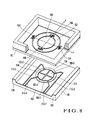
- the second potential is applied to the metal layer 156 through the lower substrate 101 and supports 104, which are made of single-crystal silicon. Instead, an insulating layer 102 on a lower substrate 101 may partially be removed to form contact holes 109, as shown in Fig. 5. Supports 108 made of, e.g., Au may be formed on the contact holes 109 to apply the second potential to a metal layer 156 through the supports 108. This facilitates electrical connection to the supports 108.
- an oxide film on the surface of the metal layer 105 or 156 or the supports 107 and 108 may be removed by, e.g., an acid. Not only mechanical contact but also solder such as an AuSn alloy or a conductive adhesive such as Ag paste can ensure electrical connection between the metal layers 105 and 156 or electrical connection between the metal layer 156 and the supports 107 or 108.
- Fig. 6 The fourth embodiment of the present invention will be described next with reference to Fig. 6.
- the same reference numerals as in Figs. 1 and 2 denote the same parts in Fig. 6.
- an antistatic structure exists on the side of a lower substrate 101. Since the first potential is supplied to driving electrodes 103-1 to 103-4 normally through a metal interconnection, the potential of the driving electrodes 103-1 to 103-4 is never indeterminate. Hence, the problem that the voltage of the driving electrodes 103-1 to 103-4 does not follow the voltage applied to the interconnection is avoidable.
- Electrically stray parts with an indeterminate potential can be classified into several parts.
- An example of such parts is the lower substrate 101.
- a mirror 153 has a larger area than the counter driving electrodes 103-1 to 103-4.
- the lower substrate itself may exist at positions facing the mirror 153. If the potential of the lower substrate 101 is different from that of the mirror 153, an electrostatic force corresponding to charges present in the lower substrate 101 facing the mirror 153 acts on the mirror 153. The charges gradually move to the first potential side through a resistance R4 in Fig. 3 or to the side of the second potential through a resistance R3. Hence, the mirror 153 drifts.
- the antistatic structure is formed in the following way.
- the lower substrate 101 uses a conductive material (single-crystal silicon in this embodiment).
- An oxide film on the lower or side surfaces of the lower substrate 101 is removed.
- a metal layer 110 is deposited at portions without the oxide film.
- the second potential is applied to the lower substrate 101 through the metal layer 110. This structure decreases the grounding resistance R3 in Fig. 3.
- the lower substrate 101 uses a conductive material.
- the oxide film on the lower or side surfaces of the lower substrate 101 is removed.
- the metal layer 110 is deposited at portions without the oxide film.
- the second potential is applied to the lower substrate 101 through the metal layer 110.
- the fourth embodiment ensures reliable electrical connection of the lower substrate 101.
- the next problem is insulating layers present on the surfaces of driving electrodes 103-1 to 103-4.
- an insulating layer is formed on the surface of each of the driving electrodes 103-1 to 103-4 to protect the electrode and prevent a short circuit, although not illustrated in Figs. 1, 2, 4, 5, 107, and 108.
- the insulating layers polarize upon application of the first potential to the driving electrodes 103-1 to 103-4. Even the insulating layers have a finite electrical conductivity although it is very low. Hence, charges move at a predetermined time constant and finally make the insulating layers equipotential to the driving electrodes 103-1 to 103-4.
- the distance between the driving electrodes 103-1 to 103-4 and the mirror 153 decreases by an amount corresponding to the thickness of the insulating layers.
- the force between the driving electrodes 103-1 to 103-4 and the mirror 153 that attract each other increases as the distance therebetween decreases. For this reason, the mirror 153 drifts.
- the discharge time constant of polarization in the insulating layers is normally large and ranges from several min to several hrs.
- an insulating layer 111 on the surface of each of the driving electrodes 103-1 to 103-4 has an opening 112 serving as the above-described antistatic structure, as shown in Fig. 7. This indicates removal (short circuit) of the capacitance C1 and resistance R2 in Fig. 3.
- the insulating layer 111 on the surface of each of the driving electrodes 103-1 to 103-4 has the opening 112. It is therefore possible to eliminate a portion with a large charge/discharge time constant from the vicinity of the driving electrodes 103-1 to 103-4 and prevent drift of the mirror 153.
- interconnections 113-1 to 113-4 supply a first potential to driving electrodes 103-1 to 103-4, respectively.
- Metal layers 114 are formed around the driving electrodes 103-1 to 103-4.
- the fifth embodiment allows to avoid polarization/discharge in the insulating layers on the driving electrodes 103-1 to 103-4.
- the next problem is an insulating layer 102 on the surface of a lower substrate 101. It is easy to remove the insulating layers on the driving electrodes 103-1 to 103-4, as in the fifth embodiment. However, it is often impossible to remove the insulating layer 102 because the driving electrodes 103-1 to 103-4 and interconnections are formed on the insulating layer 102.
- the metal layers 114 serving as the antistatic structure are formed around the driving electrodes 103-1 to 103-4 on the insulating layer 102.
- a second potential is applied to the metal layers 114, like a mirror 153.
- the area of the mirror 153 is larger than that of the driving electrodes 103-1 to 103-4.
- the insulating layer 102 around the driving electrodes 103-1 to 103-4 faces the outer peripheral portion of the mirror 153.
- the metal layers 114 are formed on the insulating layer 102 facing the mirror 153.
- the metal layers 114 can be formed simultaneously together with the driving electrodes 103-1 to 103-4 and interconnections 113-1 to 113-4.
- the insulating layer 102 on the lower substrate 101 is partially removed to form contact holes 115.
- the metal layers 114 are equipotential to the lower substrate 101. This structure facilitates electrical connection to the metal layers 114 without interconnection routing on the surface layer.
- the metal layers 114 serving as the antistatic structure are formed around the driving electrodes 103-1 to 103-4 on the insulating layer 102, and the second potential is applied to the metal layers 114. It is possible to eliminate a portion with a large charge/discharge time constant from the vicinity of the driving electrodes 103-1 to 103-4 and prevent drift of the mirror 153.
- Fig. 10 The seventh embodiment of the present invention will be described next with reference to Fig. 10.
- the same reference numerals as in Figs. 1, 2, 8, and 9 denote the same parts in Fig. 10.
- the interconnections 113-1 to 113-4 are formed on the same plane as the driving electrodes 103-1 to 103-4. As shown in Fig. 10, interconnections 113-1 to 113-4 and driving electrodes 103-1 to 103-4 may be formed on different planes.
- the interconnections 113-1 to 113-4 are formed on an insulating layer 102.
- An insulating layer 115 is deposited on the insulating layer 102 and interconnections 113-1 to 113-4.
- the driving electrodes 103-1 to 103-4 and metal layers 114 are formed on the insulating layer 115.
- Interconnections 116 connected to the metal layers 114 are formed on the insulating layer 102 simultaneously together with the interconnections 113-1 to 113-4.
- the metal layers 114 receive the same second potential as that of a mirror 153 or the second potential with an offset through the interconnections 116. This structure facilitates electrical connection to the metal layers 114 without interconnection routing on the surface layer.
- interconnections 117 may also be formed on the insulating layer 102 simultaneously together with the interconnections 113-1 to 113-4.
- Metal supports 118 to support an upper substrate 153 may be formed on the insulating layer 115 to which one end of each interconnection 117 is exposed.
- the driving electrodes 103-1 to 103-4 are spaced apart from the supports 118 by a distance (e.g., about several ⁇ m to 25 ⁇ m) not to cause discharge to the metal layers 114 and supports 118.
- a metal such as Au is deposited by, e.g., plating. This structure allows to apply the second potential to a metal layer 156 through the supports 118 and interconnections 117 and ensure potential setting on the lower surface of the mirror 153.
- the metal layer 156 may receive the second potential through a lower substrate 101 and supports 104, as in the first embodiment, instead of using the supports 118.
- the insulating layer 102 on the surface of each support 104 is partially removed to form a contact hole 106.
- a metal layer 105 made of, e.g., Au is formed on the contact hole 106.
- the metal layer 105 connects to the metal layer 156 on the side of the upper substrate 151. This structure also allows to apply the second potential to the metal layer 156 and ensure potential setting on the lower surface of the mirror 153.
- the metal layers 114 serving as the antistatic structure are formed around the driving electrodes 103-1 to 103-4 on the insulating layer 102, and the second potential is applied to the metal layers 114 through the interconnections 116. It is possible to eliminate a portion with a large charge/discharge time constant from the vicinity of the driving electrodes 103-1 to 103-4 and prevent drift of the mirror 153.
- the interconnections 116 connected to the metal layers 114 and the interconnections 117 connected to the supports 118 are separately provided. However, the interconnections may connect to each other.
- first potential ⁇ second potential In the first to seventh embodiments, first potential ⁇ second potential.
- first potential s second potential may also hold.
- Figs. 11 and 12 show an example of a conventional mirror array.
- Figs. 11 and 12 mainly partially illustrate a mirror device having a mirror as a constituent unit of a mirror array.
- a mirror array includes a plurality of mirror devices two-dimensionally arranged in a matrix.
- a mirror device 8200 has a structure in which a mirror substrate 8201 with a mirror and an electrode substrate 8301 with electrodes are arranged in parallel.
- the mirror substrate 8201 has a frame portion 8210, a movable frame 8220 arranged in an opening of the frame portion 8210 by a pair of movable frame connectors 8211a and 8211b, and a mirror 8230 that has an almost circular shape when viewed from the upper side and arranged in an opening of the movable frame 8220 by a pair of mirror connectors 8221a and 8221b.
- a frame-shaped member 8240 surrounding the movable frame 8220 and mirror 8230 is formed on the upper surface of the frame portion 8210.
- the pair of movable frame connectors 8211a and 8211b including zigzag torsion springs and provided in the notches of the movable frame 8220 connect the frame portion 8210 to the movable frame 8220.
- the pair of mirror connectors 8221a and 8221b including zigzag torsion springs and provided in the notches of the movable frame 8220 connect the movable frame 8220 to the mirror 8230.
- the electrode substrate 8301 has a plate-shaped base 8310 and a projecting portion 8320 projecting from the surface (upper surface) of the base 8310.
- the projecting portion 8320 includes a third terrace 8323 formed on the upper surface of the base 8310, a second terrace 8322 formed on the upper surface of the third terrace 8323, a first terrace 8321 formed on the upper surface of the second terrace 8322, and a pivot 8330 formed on the upper surface of the first terrace 8321.
- Each sector electrodes 8340a to 8340d are formed on the upper surface of the base 8310 including the outer surface of the projecting portion 8320.
- concave portions 8350a to 8350d that have an almost rectangular shape when viewed from the upper side are formed at positions facing the movable frame connectors 8211a and 8211b and mirror connectors 8221a and 8221b of the counter mirror substrate 8201.
- a pair of convex portions 8360a and 8360b are formed on the upper surface of the base 8310 to sandwich the first to third terraces 8321 to 8323 and the concave portions 8350a to 8350d.
- Interconnections 8370 are formed on the upper surface of the base 8310 between the concave portion 8350a and the convex portion 8360a and between the concave portion 8350c and the convex portion 8360b.
- the electrodes 8340a to 8340d connect to the interconnections 8370 through leads 8341a to 8341d.
- the above-described mirror substrate 8201 and electrode substrate 8301 form the mirror device 8200 shown in Fig. 12 by joining the lower surface of the frame portion 8210 to the upper surfaces of the convex portions 8360a and 8360b such that the mirror 8230 faces the electrodes 8340a to 8340d corresponding to it.
- a mirror array having a plurality of mirror devices 8200 arranged in a matrix is manufactured by a method to be described below.
- the mirror substrate 8201 is formed from an SOI (Silicon On Insulator) substrate.
- a side (major surface: SOI layer) of the SOI substrate with a buried insulating layer 8241 undergoes known photolithography and etching such as DEEP RIE to form, in the single-crystal silicon layer, trenches conforming to the shapes of the frame portion 8210, movable frame connectors 8211a and 8211b, movable frame 8220, mirror connectors 8221a and 8221b, and mirror 8230.
- a resist pattern with openings in predetermined regions corresponding to the trenches is formed on the lower surface of the SOI substrate.
- the silicon is selectively etched from the lower surface of the SOI substrate by using an etchant such as potassium hydroxide.
- an etchant such as potassium hydroxide.
- the opening and frame-shaped member 8240 are formed on the lower surface of the SOI substrate by using the buried insulating layer 8241 as an etching stopper layer.
- a region of the buried insulating layer 8241 exposed to the opening is removed by wet etching using hydrofluoric acid or dry etching using a CF-based gas.
- the mirror substrate 8201 having the above-described shape is formed.
- the electrode substrate 8301 is formed from, e.g., a silicon substrate.
- a silicon substrate is selectively etched by using, as a mask, a predetermined mask pattern made of a silicon nitride film or silicon oxide film and an alkaline solution such as a potassium hydroxide solution.
- the base 8310, first to third terraces 8321 to 8323, pivot 8330, concave portions 8350, and convex portions 8360a and 8360b are formed by repeating the above-described process.
- the surface of the silicon substrate on the etched side is oxidized to form a silicon oxide film.
- a metal film is formed on the silicon oxide film by, e.g., vapor deposition and patterned by known photolithography and etching to form the electrodes 8340a to 8340d, leads 8341a to 8341d, and interconnections 8370.
- the electrode substrate 8301 having the above-described shape is formed.
- the mirror substrate 8201 is bonded to the electrode substrate 8301 to form a mirror array having the mirror device 8200 that can move the mirror 8230 by applying an electric field to the electrodes 8340a to 8340d.
- a metal film such as a gold film may be formed on the upper surface of the mirror 8230.
- an electric field generated by applying individual voltages to the electrodes 8340a to 8340d through the interconnections 8370 gives an attracting force to the mirror 8230 and causes it to pivot by an angle of several degrees.
- the pivot operation of the mirror 8230 will be described with reference to Fig. 13.
- the vertical direction of Fig. 13 viewed from the front side will be called a height or depth direction.
- the upper part of Fig. 13 will be called an upper side, and the lower part of Fig. 13 will be called a lower side.
- the mirror can stably statically pivot to only an angle that is uniquely decided by the electrode structure of the electrode substrate.
- the electrodes 8340a to 8340d facing the mirror 8230 such that they can have the same area as that of the mirror 8230 and also to increase the tilt angle of the projecting portion 8320 on which the electrodes 8340a to 8340d are formed. This can be achieved by, e.g., increasing the difference of elevation of the projecting portion 8320.
- the interconnections 8370 on the electrode substrate 8301 are formed by applying a photoresist to a metal film, transferring the pattern of the interconnections 8370 to the photoresist by an exposure apparatus, and executing etching.
- the depth (depth of field) to which the exposure apparatus can precisely transfer a pattern is limited (50 to 70 ⁇ m at maximum). If exposure is done beyond this limitation, the pattern to be transferred to the photoresist defocuses so that it is difficult to form a fine interconnection pattern.
- the interconnections 8370 include a lot of interconnections, interconnection pattern formation at an accuracy of several ⁇ m is required.
- the interconnections 8370 are formed on the base 8310, i.e., on the bottom layer of the third terrace 8323 of the projecting portion 8320. Since exposure is done by setting the lower limit of focus of the exposure apparatus to the interconnections 8370, the difference of elevation of the projecting portion 8320 must be limited to 50 to 70 ⁇ m. However, to increase the pivot angle of the mirror 8230, the difference of elevation of the projecting portion 8320 must be more than the above-described limitation and, preferably, 100 ⁇ m or more. To attain this difference of elevation, it is necessary to use a special exposure apparatus with a large focus range or execute exposure a plurality of number of times for the respective elevations, resulting in an increase in the cost.
- This embodiment has been made to solve the above-described problem and has as its object to provide a mirror device capable of achieving low-voltage driving and cost reduction and increasing the pivot angle of a mirror, a mirror array, and a mirror device manufacturing method.
- Figs. 14 to 16B mainly partially illustrate a mirror device having a mirror as a constituent unit of a mirror array.
- a mirror array according to this embodiment includes a plurality of mirror devices two-dimensionally formed in a matrix.
- a mirror device has a structure in which a mirror substrate 200 with a mirror and an electrode substrate 300 with electrodes are arranged in parallel.
- the mirror substrate 200 has a plate-shaped frame portion 210 with an opening having an almost circular shape when viewed from the upper side, a movable frame 220 with an opening having an almost circular shape when viewed from the upper side and arranged in the opening of the frame portion 210 by a pair of movable frame connectors 211a and 211b, and a mirror 230 having an almost circular shape when viewed from the upper side and arranged in the opening of the movable frame 220 by a pair of mirror connectors 221a and 221b.
- a frame-shaped member 240 surrounding the movable frame 220 and mirror 230 is formed on the upper surface of the frame portion 210.
- the pair of movable frame connectors 211a and 211b including zigzag torsion springs and provided in the notches of the movable frame 220 connect the frame portion 210 to the movable frame 220.
- This structure makes the movable frame 220 pivotable about a pivot axis (movable frame pivot axis) passing through the pair of movable frame connectors 211a and 211b.
- the pair of mirror connectors 221a and 221b including zigzag torsion springs and provided in the notches of the movable frame 220 connect the movable frame 220 to the mirror 230.
- This structure makes the mirror 230 pivotable about a pivot axis (mirror pivot axis) passing through the pair of mirror connectors 221a and 221b.
- the movable frame pivot axis and mirror pivot axis intersect each other at a right angle.
- the electrode substrate 300 has a plate-shaped base 320, an outer trench 330 formed on the base 320 and having an almost rectangular shape when viewed from the upper side, and a projecting portion 340 formed in the outer trench 330 and having an almost conical shape.
- the surface of the base 320 with the outer trench 330 and projecting portion 340 has an insulating film 321.
- Four sector electrodes 360a to 360d are formed on the outer surface of the projecting portion 340 and the upper surface of the outer trench 330 to form a circle that is concentric to the mirror 230 and has the same area as the mirror 230.
- a pair of convex portions 370a and 370b are formed on an upper surface 320a of the base 320 to sandwich the outer trench 330.
- Interconnections 380 are formed on the upper surface 320a of the base 320 between the convex portions 370a and 370b and the outer trench 330. The interconnections 380 connect to the electrodes 360a to 360d through leads 361a to 361d.
- the outer trench 330 includes a concave portion formed in the surface of the base 320.
- the concave portion has a truncated pyramidal shape with an opening (upper surface) larger than the bottom surface portion.
- the projecting portion 340 is formed on the surface of the outer trench 330. When the projecting portion 340 is formed not on the base 320 but on the outer trench 330 formed in the surface of the base 320, the difference of elevation of the projecting portion 340 can increase.
- the electrodes 360a to 360d are formed on the outer trench 330 and projecting portion 340.
- the projecting portion 340 includes a third terrace 343 formed on the surface (bottom surface) of the outer trench 330 and having a truncated pyramidal shape, a second terrace 342 formed on the upper surface of the third terrace 343 and having a truncated pyramidal shape, a first terrace 341 formed on the upper surface of the second terrace 342 and having a truncated pyramidal shape, and a pivot 350 formed on the upper surface of the first terrace 341 and having a truncated pyramidal shape.
- the lower surface of the second terrace 342, i.e., the upper surface of the third terrace 343 is flush with the upper surface 320a of the base 320.
- a mirror array having a plurality of mirror devices two-dimensionally arranged in a matrix is formed by joining the mirror substrate 200 to the electrode substrate 300 with the above-described structure and, more specifically, joining the upper surfaces of the convex portions 370a and 370b of the electrode substrate 300 to the lower surface of the frame portion 210 of the mirror substrate 200 such that the mirror 230 of the mirror substrate 200 faces the electrodes 360a to 360d corresponding to the mirror 230.
- a method of manufacturing the electrode substrate 300 will be described next with reference to Figs. 17A to 20F.
- a silicon substrate 400 is oxidized to form an insulating film 401 made of SiO 2 on the surface of the silicon substrate 400, as shown in Fig. 17A.
- a photoresist material is applied to the upper surface of the insulating film 401 to form a protective film 402.
- the protective film 402 is patterned by known photolithography to form a mask pattern (pivot preformation mask pattern) 403.
- the insulating film 401 is etched by using the pivot preformation mask pattern 403 as a mask to form a mask pattern (pivot formation mask) 404 in the insulating film 401.
- This etching can be done by, e.g., known wet etching or dry etching.
- the pivot preformation mask pattern 403 is removed by, e.g., ashing.
- the silicon substrate 400 is etched by using the pivot formation mask pattern 404 as a mask to form the pivot 350.
- This etching is done by wet etching using an alkaline solution such as a potassium hydroxide solution.
- the pivot formation mask pattern 404 is removed from the upper surface of the silicon substrate 400 by, e.g., hydrofluoric acid.
- the pivot 350 is thus formed on the surface of the silicon substrate 400.
- the first terrace 341 is formed on the surface of the silicon substrate 400, as shown in Fig. 19A, in accordance with the same procedures as in Figs. 17A to 18C.
- the second terrace 342 is formed on the surface of the silicon substrate 400, as shown in Fig. 19B, in accordance with the same procedures in forming the first terrace 341.
- the outer trench 330, third terrace 343, and convex portions 370a and 370b are formed on the surface of the silicon substrate 400, as shown in Fig. 19C, in accordance with the same procedures as in forming the second terrace 342.
- the shape of the base 320 is thus formed.
- the pivot 350 is formed such that its difference of elevation, i.e., the distance from the lower surface of the third terrace 343 to the end of the pivot 350 obtains a desired value of, e.g., 100 ⁇ m.
- the upper surface of the third terrace 343 is flush with the upper surface 320a of the base 320.
- the base 320 is oxidized to form the insulating film 321 on the surface of the base 320 with the projecting portion 340.
- a metal film (metal film for electrodes/interconnections) 405 made of, e.g., A1 is formed on the surface of the base 320 with the insulating film 321 by, e.g., sputtering or vapor deposition.
- a protective film 406 made of a photoresist material is formed on the surface of the metal film 405.
- the protective film 406 is patterned by known photolithography to form a pattern 407 with the interconnection patterns of the electrodes 360a to 360d, leads 361a to 361d, and interconnections 380 shown in Figs. 14, 16A, and 16B.
- the focus of the exposure apparatus to transfer the interconnection pattern to the protective film 406 is set to the upper surface 320a of the base 320 on which the interconnections 380 are to be formed. This allows to form the interconnections 380 at the highest resolution.
- the electrodes 360a to 360d and leads 361a to 361d are located, in the height direction (vertical direction when Fig. 16A is viewed from the front side), between the first terrace 341 and the outer trench 330 formed in the upper surface 320a of the base 320, i.e., from the upper part to the lower part of the upper surface 320a of the base 320 while almost centered on the upper surface 320a.
- pattern transfer is done even for the electrodes 360a to 360d and leads 361a to 361d in a region with relatively small image defocus within or near the range where the exposure apparatus can precisely transfer the pattern. It is therefore possible to accurately form the electrodes 360a to 360d and leads 361a to 361d.
- the metal film 405 is etched by using the pattern 407 as a mask to form an interconnection layer 408 including the electrodes 360a to 360d, leads 361a to 361d, and interconnections 380 shown in Figs. 14 to 16B.
- the pattern 407 is removed by, e.g., ashing.
- the mirror array according to this embodiment which has the thus manufactured electrode substrate 300 can make the mirror 230 pivot by applying a predetermined bias voltage to all the electrodes 360a to 360d through the interconnections 380 and applying individual displacement voltages to the electrodes 360a to 360d.
- the difference of elevation of the projecting portion 340 can have a desired value of, e.g., about 100 ⁇ m.
- the projecting portion 340 can have a large tilt angle so that the mirror 230 can have a pivot angle larger than before.
- the electrodes 360a to 360d have the same size as the mirror 230 and can therefore drive the mirror 230 at a low voltage.
- Fig. 21 shows a mirror array having an outer trench with a multistage structure.
- the same names and reference numerals as in the mirror device shown in Figs. 14 to 16B denote the same constituent elements in Fig. 21, and a description thereof will be omitted as needed.
- Fig. 21 is a sectional view showing the same section as in Figs. 16A and 16B.
- An electrode substrate 301 shown in Fig. 21 has the plate-shaped base 320, a first outer trench 331 including a concave portion formed on the base 320 and having an almost rectangular shape when viewed from the upper side, a second outer trench 322 including a concave portion formed on the first outer trench 331 and having an almost rectangular shape when viewed from the upper side, and the almost conical projecting portion 340 formed on the second outer trench 332.
- the insulating film 321 is formed on the surface of the base 320 with the first outer trench 331, second outer trench 332, and projecting portion 340.
- the four sector electrodes 360a to 360d are formed on the outer surface of the projecting portion 340 and the upper surface of the second outer trench 332 to form a circle that is concentric to the mirror 230.
- the pair of convex portions 370a and 370b (not shown) are formed on an upper surface 320a of the base 320 to sandwich the first outer trench 331.
- the interconnections 380 are formed on the base 320 between the convex portions 370a and 370b and the first outer trench 331. The interconnections 380 connect to the electrodes 360a to 360d through the leads 361a to 361d.
- the first outer trench 331 includes a concave portion formed in the base 320.
- the concave portion has a truncated pyramidal shape with an upper surface larger than the bottom surface.
- the upper surface of the first outer trench 331 is flush with the upper surface of the second terrace.
- the second outer trench 332 includes a concave portion formed in the bottom surface of the first outer trench 331.
- the concave portion has a truncated pyramidal shape with an upper surface larger than the bottom surface.
- the projecting portion 340 is formed on the bottom surface of the second outer trench 332.
- the electrodes 360a to 360d are formed on the second outer trench 332 and projecting portion 340.
- the projecting portion 340 includes the third terrace 343 formed on the surface (bottom surface) of the second outer trench 332 and having a truncated pyramidal shape, the second terrace 342 formed on the upper surface of the third terrace 343 and having a truncated pyramidal shape, the first terrace 341 formed on the upper surface of the second terrace 342 and having a truncated pyramidal shape, and the pivot 350 formed on the upper surface of the first terrace 341 and having a truncated pyramidal shape.
- the lower surface of the first terrace 341, i.e., the upper surface of the second terrace 342 is flush with the surface of the base 320.
- the lower surface of the second terrace 342, i.e., the upper surface of the third terrace is flush with the upper surface of the first outer trench 331.
- the projecting portion 340 is formed such that its difference of elevation obtains a desired value of, e.g., about 100 ⁇ m.
- the exposure apparatus sets the focus on the upper surface of the base 320.
- the interconnections 380 can be formed at an accuracy of several ⁇ m. Even for the electrodes 360a to 360d and leads 361a to 361d, pattern transfer is done in a region with relatively small image defocus within or near the range where the exposure apparatus can precisely transfer the pattern. It is therefore possible to accurately form the electrodes 360a to 360d and leads 361a to 361d.
- the difference of elevation of the projecting portion 340 can have a desired value of, e.g., about 100 ⁇ m.
- the projecting portion 340 can have a large tilt angle so that the mirror 230 can have a pivot angle larger than before.
- the difference of elevation from the upper surface 320a of the base 320 to the pivot 350 can be smaller than in the electrode substrate shown in Figs. 16A and 16B.
- the defocus in the vertical direction for the upper surface 320a of the base 320 can be smaller. Consequently, more accurate pattern formation is possible.
- the mirror array having an outer trench with a multistage structure shown in Fig. 21 can be manufactured by the same manufacturing method as that for the above-described mirror array shown in Figs. 14 to 16B.
- Fig. 22 shows a mirror array having an outer trench with a divided structure.
- Fig. 22 is a sectional view showing a modification of the electrode substrate of the mirror array according to this embodiment.
- the same names and reference numerals as in the mirror device shown in Figs. 14 to 16B denote the same constituent elements in Fig. 22, and a description thereof will be omitted as needed.
- An electrode substrate 302 shown in Fig. 22 has the plate-shaped base 320, four outer trenches 333a to 333d each including a concave portion formed on the base 320 and having an almost L-shape when viewed from the upper side, and the almost conical projecting portion 340 formed on the base 320.
- An insulating film (not shown) is formed on the surface of the base 320 with the outer trenches 333a to 333d and projecting portion 340.
- the four sector electrodes 360a to 360d are formed on the upper surfaces of the mirror 230 with the insulating film, the outer trenches 333a to 333d, and the projecting portion 340 to form a circle that is concentric to the mirror 230.
- the pair of convex portions 370a and 370b are formed on the upper surface 320a of the base 320 to sandwich the outer trenches 333a to 333d.
- the interconnections 380 are formed on the upper surface 320a of the base 320 between the convex portions 370a and 370b and the outer trenches 333a to 333d.
- the interconnections 380 connect to the electrodes 360a to 360d through the leads 361a to 361d formed on the base 320.
- Each of the outer trenches 333a to 333d includes a concave portion formed in the base 320.
- the concave portion has an inverted truncated pyramidal shape with an upper surface larger than the bottom surface.
- the outer trenches 333a to 333d are formed point-symmetrically to surround the projecting portion 340 and form a rectangle concentric to the projecting portion 340 and electrodes 360a to 360d.
- the projecting portion 340 includes the second terrace 342 having a truncated pyramidal shape and formed on the upper surface 320a of the base 320 surrounded by the outer trenches 333a to 333d, the first terrace 341 formed on the upper surface of the second terrace 342 and having a truncated pyramidal shape, and the pivot 350 formed on the upper surface of the first terrace 341 and having a truncated pyramidal shape.
- the lower surface of the second terrace 342 is flush with the upper surface of the base 320, as a matter of course.
- a portion surrounded by the outer trenches 333a to 333d and having an almost truncated pyramidal shape with an upper surface corresponding to the upper surface 320a of the base 320 is equivalent to the third terrace 343 shown in Figs. 14 to 16B and 21.
- the projecting portion 340 can be formed such that its difference of elevation obtains a desired value.
- the projecting portion 340 can have a difference of elevation of, e.g., about 100 ⁇ m.
- the projecting portion 340 can have a large tilt angle so that the mirror 230 can have a pivot angle larger than before.
- Each of the leads 361a to 361d is formed between adjacent two of the outer trenches 333a to 333d on the base 320. Hence, the leads 361a to 361d and interconnections 380 are formed on the base 320.
- the exposure apparatus sets the focus on the upper surface of the base 320.
- the interconnections 380 can be formed at an accuracy of several ⁇ m.
- the leads 361a to 361d are formed on the base 320, not only the interconnections 380 but also the leads 361a to 361d can be formed at an accuracy of several ⁇ m.
- pattern transfer is done in a region with relatively small image defocus within or near the range where the exposure apparatus can precisely transfer the pattern. It is therefore possible to accurately form the electrodes 360a to 360d.
- the difference of elevation of the projecting portion 340 can have a desired value.
- the projecting portion 340 can have a large tilt angle so that the mirror 230 can have a pivot angle larger than before.
- the mirror array having divided outer trenches shown in Fig. 22 can be manufactured by the same manufacturing method as that for the above-described mirror array shown in Figs. 14 to 16B.
- the electrode substrate 300, 301, or 302 having the projecting portion 340 and the like is formed by etching the silicon substrate 400.
- the electrode substrate 300, 301, or 302 having the projecting portion 340 and the like may be formed by depositing an arbitrary substance on an arbitrary substrate.
- the mirror can have a large pivot angle.
- Interconnections are formed on the base, and the electrodes are formed on the trench formed in the substrate and the projecting portion projecting from the trench.
- a conventional mirror device will be described first.
- a conventional mirror device 8200 an electric field generated by applying individual voltages to electrodes 8340a to 8340d through interconnections 8370 gives an attracting force to a mirror 8230 and causes it to pivot by an angle of several degrees.
- the mirror 8230 is almost parallel to an electrode substrate 8301 (this state will be referred to as an initial position hereinafter), as indicated by the solid line in Fig. 13.
- the mirror 8230 tilts, as indicated by the dotted line in Fig. 13.
- FIG. 23 shows an optical switch having the mirror device 8200.
- An optical switch 8400 includes a pair of collimator arrays 8410 and 8420 each having a plurality of optical fibers arrayed two-dimensionally, and a pair of mirror arrays 8430 and 8440 each having a plurality of above-described mirror devices 8200 arrayed two-dimensionally.
- a light beam input from the collimator array 8410 serving as an input port is reflected by the mirror arrays 8430 and 8440, reaches the collimator array 8420 serving as an output port, and exits it.
- the light beam is reflected by the mirror 8230 of the mirror device 8200a and reaches a mirror device 8200b of the mirror array 8440.
- the mirror array 8440 the light beam is reflected by the mirror 8230 of the mirror device 8200b and reaches an optical fiber 8420a of the collimator array 8420, as in the mirror array 8430.
- the optical switch 8400 can spatially cross-connect the collimated light input from the collimator array 8410 to the collimator array 8420 in the form of a light beam without converting it into an electrical signal.
- identical constituent elements of the mirror devices 8200 two-dimensionally arranged in the mirror arrays 8430 and 8440 have the same shape.
- the size of the mirror 8230, the shapes of movable frame connectors 8211a and 8211b and mirror connectors 8221a and 8221b, the relative positions between the mirror 8230 and the movable frame connectors 8211a and 8211b or between the mirror 8230 and the mirror connectors 8221a and 8221b, the relative positions between the mirror 8230 and the electrodes 8340a to 8340d, and the sizes of the electrodes 8340a to 8340d do not change between the mirror devices.
- each mirror 8230 in the mirror arrays 8430 and 8440 is almost parallel to the electrode substrate 8301, as shown in Fig. 24.
- Fig. 24 schematically shows the sections of the mirrors 8230 of the plurality of mirror devices 8200 arranged in the mirror arrays 8430 and 8440.
- the mirror array 8430 has mirrors 8431 to 8435 corresponding to the mirror 8230.
- the mirror array 8440 has mirrors 8441 to 8445 corresponding to the mirror 8230.
- the mirrors 8431 to 8435 of the mirror array 8430 are almost parallel to the electrode substrate 8301 at the initial position and are arranged such that a light beam irradiates corresponding mirrors in the counter mirror array 8440.
- the mirror 8431 reflects a light beam indicated by a (to be referred to as a light beam a hereinafter) in Fig. 24 to the mirror 8441 as the counterpart of the mirror 8431.
- the mirror 8433 reflects a light beam indicated by b (to be referred to as a light beam b hereinafter) in Fig. 24 to the mirror 8443 as the counterpart of the mirror 8433.
- the mirror 8435 irradiates the mirror 8445 as the counterpart of the mirror 8435 with a light beam indicated by c (to be referred to as a light beam c hereinafter) in Fig. 24.
- a counter mirror indicates, e.g., a mirror located at the same position in the counter mirror array when one mirror array is projected from the back of the beam reflection surface, and the other mirror array is viewed from the beam reflection surface.
- the light beams that irradiate the mirrors 8431 to 8435 can irradiate arbitrary mirrors in the mirror array 8440.
- the mirror tilt angle changes depending on the position of the mirror device in the mirror array.
- the mirror 8431 tilts by 1/2 of ⁇ 1 in the positive direction (to the right in Fig. 24 viewed from the front side) from the initial position
- the light beam a irradiates the mirror 8445 of the mirror array 8440 as a target.
- the mirror 8431 must be able to tilt by 1/2 of ⁇ 1 in the positive direction from the initial position.
- the mirror 8433 When the mirror 8433 tilts by 1/2 of ⁇ 2 in the negative direction (to the left in Fig. 24 viewed from the front side) from the initial position, the light beam b irradiates the mirror 8441. When the mirror 8433 tilts by 1/2 of ⁇ 3 in the positive direction from the initial position, the light beam b irradiates the mirror 8445. Hence, to irradiate all the mirrors 8441 to 8445 of the counter mirror array 8440 with the light beam b, the mirror 8433 must be able to tilt by 1/2 of ⁇ 2 in the negative direction from the initial position and by 1/2 of ⁇ 3 in the positive direction from the initial position.
- the mirror 8435 tilts by 1/2 of ⁇ 4 in the negative direction from the initial position, the light beam c irradiates the mirror 8441.
- the mirror 8435 must be able to tilt by 1/2 of ⁇ 4 in the negative direction from the initial position.
- the mirror tilt angle changes depending on the position in the mirror array.
- the mirror devices have the same shape, all the mirror devices must be able to tilt by the same angles necessary for the mirror devices included in the same mirror array.
- the mirrors 8431 to 8435 in Fig. 24 must be able to tilt by 1/2 of ⁇ 1 in the positive direction and by 1/2 of ⁇ 4 in the negative direction.
- the mirror device using the MEMS technology has difficulty in increasing the mirror tilt angle at a low voltage, a demand has arisen for a mirror device capable of decreasing the mirror tilt angle.
- This embodiment has been made to solve the above-described problem and has as its object to provide a mirror device capable of decreasing the mirror tilt angle, a mirror array, and an optical switch.
- Figs. 25A and 25B mainly partially illustrate a mirror device having a mirror as a constituent unit of a mirror array.
- a mirror device 2 has a structure in which a mirror substrate 200 with a mirror and an electrode substrate 300 with electrodes are arranged in parallel.
- a pivot (fulcrum projection) 350 formed from an almost columnar projection exists on the upper surface of a first terrace 341 of the electrode substrate 300 at a point shifted from the center of the upper surface.
- a projecting portion 320 of the electrode substrate 300 faces a mirror 230 of the mirror substrate 200.
- the position of the pivot 350 shifts from the central axis perpendicular to the plane of the mirror 230. That is, when the center of the mirror 230 is projected to the electrode substrate 300, the center of the mirror 230 and the pivot 350 are located at different points on the electrode substrate 300 without coincidence.
- the distance and direction of movement of the pivot 350 from almost the center of the first terrace 341 are set in accordance with the position of the mirror device 2 in the mirror array.
- a pivot 8330 faces almost the center of the mirror 8230. For this reason, when a uniform voltage is applied to the electrodes 8340a to 8340d, a uniform attracting force acts on the entire mirror 8230.
- the mirror 8230 approaches the side of the electrode substrate 8301 and contacts the pivot 8330.
- the mirror 8230 is almost parallel to the electrode substrate 8301, i.e., perpendicular to the axis (indicated by the alternate long and short dashed line in Fig. 26) of the pivot 8330.
- the position of the pivot 350 shifts from the center of the mirror 230 facing the pivot 350.
- a uniform voltage to be referred to as a bias voltage hereinafter
- the mirror 230 contacts the pivot 350 and tilts by a predetermined angle from a state (indicated by the dotted line in Fig. 27) wherein the mirror is perpendicular to the axis (indicated by the alternate long and short dashed line in Fig. 27) of the pivot 350 (this state will be referred to as an initial state hereinafter).
- individual displacement voltages are applied to the electrodes 360a to 360d in this state, thereby tilting the mirror 230 on the pivot 350.
- a mirror array according to this embodiment and an optical switch having the mirror array will be described next.
- mirror devices 2 described with reference to Figs. 25A, 25B, and 27 are two-dimensionally arranged in a matrix.
- an optical switch 600 includes a pair of collimator arrays 610 and 620 each having a plurality of optical fibers arrayed two-dimensionally, and a pair of mirror arrays 510 and 520 each including the above-described mirror array 500.
- a light beam input from the collimator array 610 serving as an input port is reflected by the mirror arrays 510 and 520, reaches the collimator array 620 serving as an output port, and exits it.
- a light beam a that has entered from an optical fiber 610a of the collimator array 610 into the optical switch 600 irradiates a mirror device 2-1 of the mirror array 510.
- the light beam is reflected by the mirror 230 of the mirror device 2-1 and reaches a mirror device 2-2 of the mirror array 520.
- the light beam is reflected by the mirror 230 of the mirror device 2-2 and reaches an optical fiber 620a of the collimator array 620, as in the mirror array 510.
- the optical switch 600 can spatially cross-connect the collimated light input from the collimator array 610 to the collimator array 620 in the form of a light beam without converting it into an electrical signal.
- the position (indicated by a dotted circle in Fig. 28) of the pivot 350 of each mirror device shifts from the center (indicated by ⁇ in Fig. 28) of the mirror 230 to reflect a light beam to a mirror located at the center of the counter mirror array in the initial state.
- the pivot 350 of each mirror device 2 exists on a straight line that connects a mirror device 2a located at the center of the mirror array 500 to the center of the mirror 230 of the mirror device 2.
- the position of the pivot 350 of each mirror device 2 gradually separates from the center of the mirror 230 of the mirror device 2 to the opposite side of the mirror device 2a.
- the pivot 350 of the mirror device 2a exists at a position facing the center of the mirror 230. Hence, when a bias voltage is applied to the electrodes 360a to 360d of each mirror device 2 of the mirror array 500, the mirror 230 contacts the pivot 350 and tilts to reflect a received light beam to the mirror at the center of the counter mirror array.
- Fig. 30 is a schematic view of the sections of the mirror arrays 510 and 520.
- Fig. 30 schematically illustrates the sections of the mirrors 230 of the plurality of mirror devices 2 arranged in the mirror arrays 510 and 520.
- Each of mirrors 511 to 515 of the mirror array 510 and mirrors 521 to 525 of the mirror array 520 corresponds to the above-described mirror 230.
- each of the mirrors 511 to 515 tilts at a predetermined angle depending on the position in the mirror array 510, as shown in Fig. 30.
- the mirrors 511 to 515 tilt to reflect a light beam input to the mirror array 510 to the mirror 523 located at the center of the mirror array 520.
- the mirrors 511 to 515 need only be able to tilt by almost the same angle in the positive direction (to the right in Fig. 30 viewed from the front side) and negative direction (to the left in Fig. 30 viewed from the front side).
- the mirror 511 in Fig. 30 tilts by 1/2 of ⁇ 5 in the negative direction from the initial state
- the light beam a irradiates the mirror 521.
- the mirror 511 tilts by 1/2 of ⁇ 6 in the positive direction from the initial state the light beam a irradiates the mirror 525.
- the mirror 511 need only be able to tilt by 1/2 of ⁇ 5 in the negative direction and by 1/2 of ⁇ 6 in the positive direction from the initial state.
- a light beam c irradiates the mirror 521.
- the mirror 515 tilts by 1/2 of ⁇ 8 in the positive direction from the initial state the light beam c irradiates the mirror 525.
- the mirror 515 need only be able to tilt by 1/2 of ⁇ 7 in the negative direction and by 1/2 of ⁇ 8 in the positive direction from the initial state.
- the mirror 511 need only be able to tilt by 1/2 of ⁇ 5 in the negative direction and by 1/2 of ⁇ 6 in the positive direction from the initial state, as described above.
- This angle is smaller than and, more specifically, about 1/2 the tilt angle of the mirror 230 of the mirror device 8200 in the conventional mirror array 8430.
- the mirror array according to this embodiment can decrease the mirror tilt angle. Hence, the driving voltage of the mirror device and mirror array can be low.
- the mirror substrate 200 is formed from an SOI (Silicon On Insulator) substrate.
- a side (major surface: SOI layer) of the SOI substrate with a buried insulating layer 250 undergoes known photolithography and etching such as DEEP RIE to form, in the single-crystal silicon layer, trenches conforming to the shapes of a frame portion 210, movable frame connectors 211a and 211b, movable frame 220, mirror connectors 221a and 221b, and mirror 230.
- photolithography and etching such as DEEP RIE
- a resist pattern with openings in predetermined regions corresponding to the trenches is formed on the lower surface of the SOI substrate.
- the silicon is selectively etched from the lower surface of the SOI substrate by dry etching using, e.g., SF 6 .
- an opening and a frame-shaped member 240 are formed on the lower surface of the SOI substrate by using the buried insulating layer 250 as an etching stopper layer.
- the etching of silicon may be wet etching using, e.g., potassium hydroxide.
- a region of the buried insulating layer 250 exposed to the opening is removed by dry etching using, e.g., CF 6 . With this process, the mirror substrate 201 is formed.
- the buried insulating layer 250 may be removed by using hydrofluoric acid.
- the electrode substrate 8301 is formed from, e.g., a silicon substrate.
- a silicon substrate is selectively etched by using, as a mask, a predetermined mask pattern made of a silicon nitride film or silicon oxide film and a potassium hydroxide solution.
- a base 310, first and second terraces 321 and 322, pivot 350, and convex portions 360a and 360b are formed by repeating the above-described process.
- the pivot 350 is formed at a position shifted from the center of a first terrace 341 depending on the position in the mirror array 500.
- the pivot 350 of the mirror device 2 at the center of the mirror array 500 is formed almost at the center of the first terrace 341.
- the surface of the silicon substrate on the etched side is oxidized to form a silicon oxide film.
- a metal film is formed on the silicon oxide film by, e.g., vapor deposition and patterned by known photolithography and etching to form the electrodes 360a to 360d, leads 341a to 341d, and interconnections 370. With this process, the electrode substrate 300 having the above-described shape is formed.
- the mirror substrate 20 is bonded to the electrode substrate 300 to form the mirror array 500 having the mirror device 2 that moves the mirror 230 by applying an electric field to the electrodes 360a to 360d.
- the position of the pivot 350 of each mirror device 2 of the thus manufactured mirror array 500 is adjusted in accordance with its position in the mirror array 500.
- Each mirror device reflects a light beam to the mirror at the center of the counter mirror array 520 upon applying a bias voltage to the electrodes 360a to 360d. This allows to decrease the tilt angle of the mirror 230 of each mirror device 2.
- the mirror array 500 shown in Fig. 28 has 5 ⁇ 5 mirror devices 2.
- the number of mirror devices 2 provided in the mirror array 500 is not limited to 5 ⁇ 5 and can freely be set as needed.
- the mirror array 520 may have the same structure as the mirror array 510.
- the mirror 230 of the mirror device 2 need not always tilt one-dimensionally, as shown in Fig. 30.
- the mirror 230 may tilt two-dimensionally about the movable frame pivot axis and the mirror pivot axis.
- the position of the pivot 350 of the mirror device 2 on the first terrace 341 is two-dimensionally adjusted depending on the position in the mirror array 500 of the mirror device 2.
- the pivot 350 is provided on the projecting portion 320.
- the pivot 350 may exist on the electrode substrate 300.
- the electrodes 360a to 360d are formed on the electrode substrate 300.
- a bias voltage and displacement electrodes are applied to the electrodes 360a to 360d.
- only the displacement voltages may be applied.
- no third terrace 343 is formed on a projecting portion 340.
- the present invention is also applicable to a mirror device with the third terrace 343.
- no outer trench is formed in this embodiment, the present invention is also applicable to a mirror device with an outer trench.
- the mirror device 2 and mirror array according to this embodiment are usable not only in an optical switch but also in a measurement device, display, and scanner.
- the pivot 350 of the mirror device 2 is provided at an arbitrary position in accordance with the application purpose and specifications.
- the mirror tilts by a predetermined angle when a bias voltage is applied to the electrodes. Since the mirror tilts from this tilted state, the tilt angle of the mirror can be small. This also allows to drive the mirror device at a low voltage.
- a connector and a counter connector have different structures to decrease the mirror tilt angle.
- Fig. 31 mainly partially illustrates a mirror device 2 having a mirror as a constituent unit of a mirror array.
- a mirror array according to this embodiment includes a plurality of mirror devices two-dimensionally arranged in a matrix.
- the mirror device 2 has a structure in which a mirror substrate 200 with a mirror and an electrode substrate 300 with electrodes are arranged in parallel.
- the mirror substrate 200 has a plate-shaped frame portion 210 with an opening having an almost circular shape when viewed from the upper side, a movable frame 220 with an opening having an almost circular shape when viewed from the upper side and arranged in the opening of the frame portion 210 by a pair of movable frame connectors 211a and 211b, a mirror 230 having an almost circular shape when viewed from the upper side and arranged in the opening of the movable frame 220 by a pair of mirror connectors 221a and 221b, and a frame-shaped member 240 formed on the upper surface of the frame portion 210 to surround the movable frame 220 and mirror 230.
- the pair of movable frame connectors 211a and 211b including zigzag torsion springs and provided in first notches 222a and 222b of the movable frame 220 connect the frame portion 210 to the movable frame 220.
- This structure makes the movable frame 220 pivotable about a movable frame pivot axis passing through the pair of movable frame connectors 211a and 211b.
- the movable frame connectors 211a and 211b have different structures and, more particularly, different spring constants. In, e.g., Fig. 31, the movable frame connector 211a is thicker than the movable frame connector 211b. Hence, the spring constant of the movable frame connector 211a is larger than that of the movable frame connector 211b.
- the pair of mirror connectors 221a and 221b including zigzag torsion springs and provided in second notches 223a and 223b of the movable frame 220 connect the movable frame 220 to the mirror 230.
- This structure makes the mirror 230 pivotable about a mirror pivot axis passing through the pair of mirror connectors 221a and 221b.
- the mirror connectors 221a and 221b have different structures and, more particularly, different spring constants. In, e.g., Fig. 31, the mirror connector 221a is thicker than the mirror connector 221b. Hence, the spring constant of the mirror connector 221a is larger than that of the mirror connector 221b.
- the movable frame pivot axis and mirror pivot axis intersect each other at a right angle.
- Fig. 32 is a schematic view of a torsion spring included in the movable frame connectors 211a and 211b and mirror connectors 221a and 221b.
- the spring constants of the movable frame connectors 211a and 211b and mirror connectors 221a and 221b of the mirror array according to this embodiment mainly indicate spring constants in the distance direction of the mirror substrate 200 and electrode substrate 300, i.e., the Z-axis direction.
- the order of the spring constants in the Z-axis direction depends on the following elements.
- the order of the spring constants in the Z-axis direction depends on an X-direction length 11 of the torsion spring in Fig. 32.
- the order of the spring constants in the Z-axis direction also depends on a Y-direction length 12 of the torsion spring in Fig. 32.
- the order of the spring constants in the Z-axis direction also depends on a width t of the torsion spring in Fig. 32.
- the order of the spring constants in the Z-axis direction also depends on an interval p between adjacent torsion spring elements, i.e., the pitch of the zigzag of the torsion spring in Fig. 32.
- the order of the spring constants in the Z-axis direction also depends on a number n of times of turn of the zigzag of the torsion spring in Fig. 32.
- the order of the spring constants in the Z-axis direction also depends on a thickness h of the torsion spring in Fig. 32.
- At least one of the above-described elements changes between a pair of members, i.e., the movable frame connectors 211a and 211b and mirror connectors 221a and 221b. This causes each of the movable frame connectors 211a and 211b and mirror connectors 221a and 221b to have a spring constant different from that of the counterpart.
- Figs. 33A to 34B show the relationship between the width and the spring constant of a torsion spring made of, e.g., Si and having a simple beam structure with a rectangular section.
- the ordinate on the right side represents the spring constant of rotation about the longitudinal axis, i.e., the X-axis of the torsion spring.
- the ordinate on the left side represents the spring constant in the height direction, i.e., the Z-axis direction of the torsion spring.
- the abscissa represents the width, i.e., Y-direction length of the torsion spring.
- a curve a indicates the relationship between the spring constant of rotation about the X-axis of the torsion spring and the width of the torsion spring.
- a curve b indicates the relationship between the spring constant in the Z-axis direction of the torsion spring and the width of the torsion spring.
- the spring constant in the Z-axis direction of the torsion spring should change, it is necessary to set a torsion spring shape that does not change the spring constants in the X and Y directions and the spring constant of rotation about the X-axis of the torsion spring.
- the spring constants in the X and Y directions and the spring constant of rotation about the X-axis of the torsion spring are fixed to arbitrary values.
- the spring constant of rotation about the X-axis is set to 1.0 ⁇ 10 -8 .
- the torsion spring width is calculated as 1.8 ⁇ m from the curve a
- the spring constant in the Z-axis direction is calculated as 69 from the curve b.
- the X-direction length of the torsion spring in Fig. 33B changes to 210 ⁇ m
- the spring constant of rotation about the X-axis is 1.0 ⁇ 10 -8 , like the torsion spring in Fig. 33B.
- the torsion spring width is calculated as 1.9 ⁇ m from the curve a
- the spring constant in the Z-axis direction is calculated as 47 from the curve b.
- the spring constant in the Z-axis direction of the torsion spring can change without changing the spring constant of rotation about the X-axis of the torsion spring.
- Figs. 35 and 36 illustrate the sections of the main part taken along a line I - I in Fig. 31 so as to explain the relationship between the mirror 230 and the mirror connectors 221a and 221b.
- Figs. 35 and 36 explain a mirror device having flat electrodes without any projecting portion as an example. However, this embodiment is also applicable to a mirror device having a projecting portion.
- Figs. 35 and 36 also explain a mirror device without any outer trench as an example. However, this embodiment is also applicable to a mirror device having an outer trench.
- mirror connectors 8221a and 8221b have the same structure.
- two ends of a mirror 8230 supported by the mirror connectors 8221a and 8221b are connected to a movable frame 8220 by the same suspending force.
- a uniform voltage is applied to electrodes 8340a to 8340d, a uniform attracting force acts on the entire mirror 8230.
- the mirror 8230 becomes almost parallel to a base 8310, as indicated by the dotted line in Fig. 35.
- the mirror connectors 221a and 221b serving as a pair of members have different structures and, more particularly, different spring constants.
- two ends of the mirror 230 supported by the mirror connectors 221a and 221b are connected to the movable frame 220 by different suspending forces.
- a uniform voltage to be referred to as a bias voltage hereinafter
- the mirror 230 tilts by a predetermined angle with respect to a base 310 (this state will be referred to as an initial state hereinafter), as indicated by the dotted line in Fig. 36.
- the movable frame connector 211a has a spring constant larger than that of the movable frame connector 211b
- the mirror connector 221a has a spring constant larger than that of the mirror connector 221b.
- the mirror 230 that is parallel to the movable frame 220 tilts to the side of the base 300 while reducing the distance to the base 300 in the X direction (this motion will be referred to as "tilt in the X direction” hereinafter).
- the mirror 230 that is parallel to the frame portion 210 tilts to the side of the base 310 while reducing the distance to the base 300 in a direction of an arrow a in Fig. 31 (this motion will be referred to as "tilt in the a direction” hereinafter).
- the mirror 230 is tilted by applying individual control voltages to the electrodes 340a to 340d in this state.
- Fig. 37 shows an example of a mirror array including the mirror devices 2 according to this embodiment.
- Fig. 37 illustrates a state wherein a predetermined bias voltage is applied to the electrodes 340a to 340d.
- Each mirror device shown in Fig. 37 is in the state shown in Fig. 31 viewed from the front side. That is, each mirror device has the mirror connectors 221a and 221b in the horizontal direction and the movable frame connectors 211a and 211b in the vertical direction.
- a mirror array 700 the mirror devices 2 described with reference to Figs. 31 and 36 are two-dimensionally arranged in a matrix.
- the mirror array 700 corresponds to the mirror arrays 510 an 520 of the optical switch 600 shown in Fig. 29.
- each of the movable frame connectors 211a and 211b and mirror connectors 221a and 221b in each mirror device has a spring constant different from the counterpart so that the mirror 230 reflects a light beam to a mirror located at the center of the counter mirror array in the initial state wherein a uniform bias voltage is applied to the electrodes 340a to 340d.
- each of the movable frame connectors 211a and 211b and mirror connectors 221a and 221b has the same spring constant as the counterpart.
- the spring constant in the Z-axis direction of the mirror connector 221a is larger than that of the mirror connector 221b such that the mirror 230 tilts in the X direction more than in the mirror device 2a in the initial state.
- the mirror 230 tilts in the X direction more than the mirror 230 of the mirror device 2b in the initial state.
- the spring constant in the Z-axis direction of the mirror connector 221a of the mirror device 2c is set larger than that of the mirror connector 221b of the mirror device 2b.
- the spring constant in the Z-axis direction of the movable frame connector 211a is larger than that of the movable frame connector 211b such that the mirror 230 tilts in the Y direction more than in the mirror device 2a in the initial state.
- the mirror 230 tilts in the Y direction more than the mirror 230 of the mirror device 2d in the initial state.
- the spring constant in the Z-axis direction of the movable frame connector 211a of the mirror device 2e is set larger than that of the movable frame connector 211b of the mirror device 2d.
- the spring constant in the Z-axis direction of the movable frame connector 211a is larger than that of the movable frame connector 211b
- the spring constant in the Z-axis direction of the mirror connector 221a is larger than that of the mirror connector 221b such that the mirror 230 tilts in the X and Y directions, i.e., in the direction of the arrow a (to be referred to as an "a direction” hereinafter) in Fig.
- the mirror 230 tilts in the a direction more than the mirror 230 of the mirror device 2f in the initial state.
- the spring constants in the Z-axis direction of the movable frame connector 211a and mirror connector 221a of the mirror device 2f are set larger than those of the movable frame connector 211b and mirror connector 221b of the mirror device 2f.
- the mirror 230 tilts in the X direction similarly as in the mirror devices 2c and 2g and in the Y direction similarly as in the mirror devices 2d and 2f in the initial state.
- the movable frame connectors 211b and mirror connectors 221b of the mirror devices 2c, 2d, 2f, 2g, and 2h have the same spring constants in the Z-axis direction
- the movable frame connector 211a of the mirror device 2h has the same spring constant in the Z-axis direction as that of the movable frame connectors 211a of the mirror devices 2d and 2f.
- the mirror connector 221a of the mirror device h has the same spring constant in the Z-axis direction as that of the mirror connectors 221a of the mirror devices 2c and 2g.
- the movable frame connectors 211a and 211b and mirror connectors 221a and 221b have spring constants set depending on the position in the mirror array 700.
- a bias voltage having a uniform magnitude is applied to the electrodes 340a to 340d, the mirror 230 of each mirror device 2 of the mirror array 700 tilts to reflect a received light beam to the mirror at the center of the counter mirror array. This reflecting operation is the same as that described in the ninth embodiment with reference to Fig. 30.
- Fig. 30 is a sectional view taken along a line II - II in Fig. 37.
- Fig. 30 schematically illustrates the sections of the mirrors 230 of the plurality of mirror devices 2 arranged in mirror arrays 510 and 520 each including the mirror array 700.
- Each of mirrors 511 to 515 of the mirror array 510 and mirrors 521 to 525 of the mirror array 520 corresponds to the mirror 230 of the mirror device 2 included in the above-described mirror array 700.
- the mirror arrays 510 and 520 shown in Fig. 30 correspond to the mirror arrays 510 and 520, respectively, of the optical switch 600 shown in Fig. 29.
- each of the movable frame connectors 211a and 211b and mirror connectors 221a and 221b has a spring constant different from that of the counterpart. Since the mirror tilts by a predetermined angle in the initial state, the mirror tilt angle can be small consequently.
- the mirror device and mirror array according to this embodiment are manufactured by the same manufacturing method as in the above-described ninth embodiment.
- the movable frame connectors 211a and 211b and mirror connectors 221a and 221b are formed while changing the spring constant depending on the position in the mirror array.
- each mirror device 2 of the thus manufactured mirror array 700 The spring constants of the movable frame connectors 211a and 211b and mirror connectors 221a and 221b of each mirror device 2 of the thus manufactured mirror array 700 are adjusted in accordance with its position in the mirror array 700.
- Each mirror device reflects a light beam to the mirror at the center of a counter mirror array 80 upon applying a predetermined bias voltage to the electrodes 340a to 340d. This allows to decrease the tilt angle of the mirror 230 of each mirror device 2.
- Fig. 38 shows a modification of the mirror substrate 200.
- the movable frame connectors 211a and 211b are provided in the first notches 222a and 222b formed in the movable frame 220.
- the movable frame connectors 211a and 211b need not always exist there and may exist in third notches 224a and 224b formed in the frame portion 210, as shown in Fig. 38.
- the electrodes 340a to 340d need not always exist on the base 310 and may exist on, e.g., a projecting portion provided on the base 310. Alternatively, the electrodes 340a to 340d may exist on the projecting portion and base 310.
- the mirror array 700 shown in Fig. 37 has 5 ⁇ 5 mirror devices 2.
- the number of mirror devices 2 provided in the mirror array 700 is not limited to 5 ⁇ 5 and can freely be set as needed.
- the mirror array 80 of this embodiment may have the same structure as the mirror array 700.
- the mirror device 2 and mirror array according to this embodiment are usable not only in an optical switch but also in a measurement device, display, and scanner.
- the projecting portion 320 and electrodes 340a to 340d are provided at arbitrary positions in accordance with the application purpose and specifications.
- the mirror 230 is tilted in the initial state by adjusting the spring constant in the Z-axis direction of a torsion spring included in each of the movable frame connectors 211a and 211b and mirror connectors 221a and 221b.
- the spring constant of rotation about the X-axis of the torsion spring may be adjusted. Even this can make the mirror 230 tilt in the initial state.
- a bias voltage and displacement electrodes are applied to the electrodes 340a to 340d.
- the displacement voltages may be applied.
- each connector has a structure different from that of the counter connector so that the mirror tilts by a predetermined angle in accordance with bias voltage application to the electrodes. Since the mirror is tilted by applying control voltages in this tilted state, the mirror tilt angle can be small. Even when it is necessary to tilt the mirror largely, it can operate at a low voltage.
- Figs. 39A and 39B mainly partially illustrate a mirror device 2 having a mirror as a constituent unit of a mirror array. In this embodiment, a mirror device having flat electrodes without any projecting portion will be described as an example.
- the mirror device 2 has a structure in which a mirror substrate 200 with a circular mirror 230 and an electrode substrate 300 with electrodes 340a to 340d are arranged in parallel. As shown in Figs. 39A and 39B, the electrodes 340a to 340d are formed at arbitrary positions on the electrode substrate 300 asymmetrically with respect to at least one of the movable frame pivot axis and mirror pivot axis of the mirror 230 projected onto the electrode substrate 300.
- the electrodes 340a to 340d have a sector shape obtained by dividing a circle with the same size as the mirror 230 into four parts of uniform size along parting lines parallel to the movable frame pivot axis and mirror pivot axis.
- the center of the electrodes 340a to 340d indicates the center of the circle.
- the center passes through the intersection of the parting lines.
- the distance and direction of movement of the electrodes 340a to 340d from almost the center of the electrode substrate 300 are set in accordance with the position of the mirror device 2 in the mirror array.
- the parting lines need not always include only straight lines but may include arbitrary curves.
- electrodes 8340a to 8340d are formed at positions on a base 8310 symmetrically with respect to the movable frame pivot axis and mirror pivot axis of a mirror 8230 projected onto an electrode substrate 8301.
- the central axis (indicated by the alternate long and short dashed line in Fig. 40) of the mirror 8230 matches the central axis (indicated by the alternate long and two short dashed line in Fig. 40) of the electrodes 8340a to 8340d.
- a uniform voltage is applied to the electrodes 8340a to 8340d, a uniform attracting force acts on the entire mirror 8230.
- the mirror 230 is almost parallel to the major surface of the base 8310 of the electrode substrate 8301, i.e., almost perpendicular to the central axis of the mirror 8230.
- the central axis of the mirror 230 indicates a straight line that passes through the center of the mirror 8230 and is perpendicular to the plane of the mirror 8230, i.e., parallel to the distance direction between a mirror substrate 8201 and the electrode substrate 8301.
- the central axis of the electrodes 8340a to 8340d indicates a straight line that passes through the center of the electrodes 8340a to 8340d and is parallel to the planes of the electrodes 8340a to 8340d, i.e., the distance direction between a mirror substrate 8201 and the electrode substrate 8301.
- the electrodes 340a to 340d are formed at positions on the base 310 asymmetrically with respect to at least one of the movable frame pivot axis and mirror pivot axis of the mirror 230 projected onto the electrode substrate 300.
- the central axis (indicated by the alternate long and short dashed line in Fig. 41) of the mirror 230 does not match the central axis (indicated by the alternate long and two short dashed line in Fig. 41) of the electrodes 340a to 340d.
- a uniform voltage (to be referred to as a bias voltage hereinafter) is applied to the electrodes 340a to 340d
- an attraction acts on a portion facing the electrodes 340a to 340d.
- the mirror 230 tilts by a predetermined angle (this state will be referred to as an "initial state” hereinafter) from a state (indicated by the dotted line in Fig. 41) wherein the mirror is perpendicular to the central axis.
- the mirror 230 is tilted by applying individual control voltages to the electrodes 340a to 340d in this state.
- a mirror array 800 according to this embodiment, the mirror devices 2 described with reference to Figs. 39A, 39B, and 41 are two-dimensionally arranged in a matrix.
- the mirror array 800 corresponds to the mirror arrays 510 an 520 of the optical switch 600 shown in Fig. 29.
- the electrodes 340a to 340d (indicated by the dotted line in Fig. 42) of each mirror device are formed at positions on the electrode substrate 300 asymmetrically with respect to the pivot axis of the mirror 230 projected onto the electrode substrate 300 so that the mirror 230 reflects a light beam to a mirror located at the center of the counter mirror array in the initial state. It is also possible to adjust the tilt of the mirror 230 by the magnitude of a bias voltage.
- the electrodes 340a to 340d of each mirror device 2 exist on a straight line that connects a mirror device 2a located at the center of the mirror array 800 to the center of the mirror 230 of the mirror device 2.
- the positions of the electrodes 340a to 340d of each mirror device 2 gradually separate from the center of the mirror 230 of the mirror device 2 to the opposite side of the mirror device 2a.
- This arrangement increases the tilt of the mirror 230 as the distance between the mirror device 2a and the mirror device 2 increases.
- the central axis of the electrodes 340a to 340d of the mirror device 2a matches the central axis of the mirror 230.
- Fig. 30 is a sectional view taken along a line I - I in Fig. 42.
- Fig. 30 schematically illustrates the sections of the mirrors 230 of the plurality of mirror devices 2 arranged in mirror arrays 510 and 520 each including the mirror array 800.
- Each of mirrors 511 to 515 of the mirror array 510 and mirrors 521 to 525 of the mirror array 520 corresponds to the above-described mirror 230.
- the mirror arrays 510 and 520 shown in Fig. 30 correspond to the mirror arrays 510 and 520 of the optical switch 600 shown in Fig. 29, respectively.
- the mirror device and mirror array according to this embodiment are manufactured by the same manufacturing method as in the above-described ninth embodiment.
- the electrodes 340a to 340d are formed at positions shifted from the center of a base 310 depending on the position in the mirror array 800.
- the electrodes 340a to 340d of the mirror device 2 located at the center of the mirror array 800 are formed almost at the center of the base 310. With this process, the electrode substrate 300 having the above-described shape is formed.
- each mirror device 2 of the thus manufactured mirror array 800 The positions of the electrodes 340a to 340d of each mirror device 2 of the thus manufactured mirror array 800 are adjusted in accordance with its position in the mirror array 800.
- Each mirror device reflects a light beam to the mirror at the center of the counter mirror array 800 upon applying a uniform bias voltage to the electrodes 340a to 340d. This allows to decrease the tilt angle of the mirror 230 of each mirror device 2. Additionally, since the mirror 230 tilts in the initial state, the operation range of the mirror 230 is small, and consequently, low voltage driving is possible.
- the electrodes are provided at arbitrary positions on the substrate asymmetrically with respect to the pivot axis of the mirror projected onto the electrode substrate.
- the mirror tilts by a predetermined angle in accordance with bias voltage application to the electrodes. Since the mirror is tilted by applying a control voltage in the tilted state, the mirror tilt angle can be small. Since the tilt angle is small, low voltage driving is possible.
- a projecting portion is provided on the electrode substrate 300 of the 11th embodiment, and electrodes 340a to 340d are provided on the projecting portion and electrode substrate 300, as shown in Figs. 43 and 44.
- the same names and reference numerals as in the 11th embodiment denote the same constituent elements in the 12th embodiment, and a description thereof will be omitted as needed.
- a mirror device 2 has a structure in which a mirror substrate 200 with a mirror and an electrode substrate 300 with electrodes are arranged in parallel.
- the electrode substrate 300 has a plate-shaped base 310 and a conical projecting portion 320 projecting from the surface (upper surface) of the base 310.
- the projecting portion 320 includes a second terrace 322 having a truncated pyramidal shape and formed on the upper surface of the base 310, a first terrace 321 having a truncated pyramidal shape and formed on the upper surface of the second terrace 322, and a pivot 330 having a columnar shape and formed on the upper surface of the first terrace 321.
- the projecting portion 320 has the center formed at a position shifted from the center of the base 310 depending on the position in a mirror array. The distance and direction of movement of the projecting portion 320 from the center of the base 310 are set in accordance with the position of the mirror device 2 in the mirror array.
- the four sector electrodes 340a to 340d are formed on the upper surface of the base 310 including the outer surface of the projecting portion 320 in a circle with the same size as a mirror 230 of the counter mirror substrate 200.
- the center of the electrodes 340a to 340d almost matches the center of the pivot 330.
- the position of the projecting portion 320 shifts from the center of the base 310 depending on the position in a mirror array 800. Since the central axes do not match, the electrodes 340a to 340d and the mirror 230 partially overlap each other when viewed from the upper side.
- the central axis (indicated by the alternate long and short dashed line in Fig. 44) of the mirror 230 shifts from the central axis (indicated by the alternate long and two short dashed line in Fig. 44) of the projecting portion 320 having the electrodes 340a to 340d on the surface, as shown in Fig. 44.
- the mirror 230 tilts by a predetermined angle (this state will be referred to as an "initial state” hereinafter) from a state (indicated by the dotted line in Fig. 44) wherein the mirror is perpendicular to the central axis.
- the mirror 230 is tilted by applying individual control voltages to the electrodes 340a to 340d in this state.
- a mirror array 800 shown in Fig. 42 is formed by arranging the mirror devices 2 two-dimensionally in a matrix.
- the central axis of the projecting portion 320 and the central axis of the electrodes 340a to 340d of each mirror device 2 exist on a straight line that connects a mirror device 2a located at the center of the mirror array 800 to the center of the mirror 230 of the mirror device 2.
- the positions of the central axes gradually separate from the center of the mirror 230 of the mirror device 2 to the opposite side of the mirror device 2a.
- the central axis of the projecting portion 320 and the central axis of the electrodes 340a to 340d of the mirror device 2a match the central axis of the mirror 230.
- a bias voltage is uniformly applied to the electrodes 340a to 340d of each mirror device 2 of the mirror array 800, the mirror 230 tilts to reflect a received light beam to the mirror at the center of the counter mirror array. This allows the mirror array according to this embodiment to reduce the mirror tilt angle.
- a method of manufacturing the mirror array according to this embodiment will be described next.
- a method of manufacturing the mirror substrate 200 is the same as in the 11th embodiment.
- the projecting portion 320 is formed at a position shifted from the center of the base 310 depending on the position in the mirror array.
- the projecting portion 320 of the mirror device 2 located at the center of the mirror array 800 is formed almost at the center of the base 310.
- the electrode substrate 300 having the above-described shape is formed.
- the position of the projecting portion 320 i.e., the positions of the electrodes 340a to 340d of each mirror device 2 of the thus manufactured mirror array 800 are adjusted in accordance with its position in the mirror array 800.
- Each mirror device reflects a light beam to the mirror at the center of the counter mirror array 800 upon applying a uniform bias voltage to the electrodes 340a to 340d. This allows to decrease the tilt angle of the mirror 230 of each mirror device 2.
- the mirror array 800 shown in Fig. 42 has 5 ⁇ 5 mirror devices 2.
- the number of mirror devices 2 provided in the mirror array 800 is not limited to 5 ⁇ 5 and can freely be set as needed.
- the mirror 230 of the mirror device 2 according to the 11th and 12th embodiments tilts not only one-dimensionally as shown in Fig. 30 but also two-dimensionally about the movable frame pivot axis and mirror pivot axis.
- the positions of the electrodes 340a to 340d and projecting portion 320 of the mirror device 2 on the electrode substrate 300 are two-dimensionally adjusted in accordance with the position of the mirror device 2 in the mirror array 800.
- the mirror device 2 and mirror array according to the 11th and 12th embodiments are usable not only in an optical switch but also in a measurement device, display, and scanner.
- the projecting portion 320 and electrodes 340a to 340d of the mirror device 2 are provided at arbitrary positions in accordance with the application purpose and specifications.
- the central axis of the mirror 230 is shifted from the central axes of the projecting portion 320 and electrodes 340a to 340d by adjusting the position of the projecting portion 320 or the positions of the electrodes 340a to 340d on the electrode substrate 300.
- the central axis of the mirror 230 may be shifted from the central axes of the projecting portion 320 and electrodes 340a to 340d by adjusting the position of the mirror 230 on the mirror substrate 200.
- a bias voltage and displacement electrodes are applied to the electrodes 340a to 340d.
- the displacement voltages may be applied.
- the electrodes exist at arbitrary positions on the substrate asymmetrically with respect to the pivot axis of the mirror projected onto the electrode substrate.
- the mirror tilts by a predetermined angle in accordance with bias voltage application to the electrodes. Since the mirror is tilted by applying control voltages in this tilted state, the mirror tilt angle can be small. Since the tilt angle is small, low voltage driving is possible.
- Fig. 45 mainly partially illustrates a mirror device 2 having a mirror as a constituent unit of a mirror array.
- a mirror device having flat electrodes without any projecting portion will be described as an example.
- the mirror device 2 has a structure in which a mirror substrate 200 with a mirror and an electrode substrate 300 with electrodes are arranged in parallel.
- the mirror substrate 200 has a plate-shaped frame portion 210 with an opening having an almost circular shape when viewed from the upper side, a movable frame 220 with an opening having an almost circular shape when viewed from the upper side and arranged in the opening of the frame portion 210 by a pair of movable frame connectors 211a and 211b, a mirror 230 having an almost circular shape when viewed from the upper side and arranged in the opening of the movable frame 220 by a pair of mirror connectors 221a and 221b, and a frame-shaped member 240 formed on the upper surface of the frame portion 210 so as to surround the movable frame 220 and mirror 230.
- the pair of movable frame connectors 211a and 211b including zigzag torsion springs and provided in first notches 222a and 222b of the movable frame 220 connect the frame portion 210 to the movable frame 220.
- This structure makes the movable frame 220 pivotable about a movable frame pivot axis passing through the pair of movable frame connectors 211a and 211b.
- the movable frame connectors 211a and 211b connect to the frame portion 210 and movable frame 220 such that the movable frame pivot axis indicated by an alternate long and short dashed line k in Fig. 45 passes through a gravity center G of the mirror 230.
- the gravity center of the mirror 230 corresponds to the center of the circle of the outside shape of the mirror 230.
- the pair of mirror connectors 221a and 221b including zigzag torsion springs and provided in second notches 223a and 223b of the movable frame 220 connect the movable frame 220 to the mirror 230.
- This structure makes the mirror 230 pivotable about a mirror pivot axis passing through the pair of mirror connectors 221a and 221b.
- the mirror connectors 221a and 221b are provided at positions translated from the mirror pivot axis of a conventional mirror device, which is indicated by a dotted line 1 and passes through the gravity center G, to the side of the movable frame connector 211b, i.e., in the Y direction shown in Fig. 45.
- the mirror pivot axis Since the mirror pivot axis is translated in the Y direction from the conventional mirror pivot axis 1, the mirror pivot axis does not pass through the gravity center of the mirror 230, as indicated by an alternate long and two short dashed line m in Fig. 45.
- the movable frame pivot axis and mirror pivot axis intersect at a right angle.
- Figs. 46 and 47 correspond the section of a main part taken along a line I - I in Fig. 45 and illustrate the relationship between the mirror pivot axis and the mirror 230.
- mirror connectors 8221a and 221b are arranged to make the mirror pivot axis pass through the gravity center G of a mirror 8230.
- the mirror 8230 is supported symmetrically with respect to the mirror pivot axis. For this reason, when a uniform voltage is applied to electrodes 8340a to 8340d, a uniform attracting force acts on the entire mirror 8230.
- the mirror 8230 and a movable frame 8220 approach the side of a base 8310 while keeping the almost parallel state to the base 8310, as indicated by the dotted line in Fig. 46.
- the mirror pivot axis m does not pass through the gravity center G of the mirror 230.
- the distance between the mirror pivot axis and the end of the mirror 230 on the side of the movable frame connector 211a is longer than the distance between the mirror pivot axis and the end of the mirror 230 on the side of the movable frame connector 211b.
- the mirror 230 When an attracting force acts on the mirror 230 upon application of a uniform voltage (to be referred to as a bias voltage hereinafter), the mirror 230 approaches to the side of the movable frame 220 and base 310 and tilts about the mirror pivot axis, as indicated by the dotted line in Fig. 47, so that the end on the side of the movable frame connector 211a is closer to the side of the base 310 (this state will be referred to as an initial state hereinafter).
- a uniform voltage to as a uniform voltage
- individual control voltages are applied to the electrodes 340a to 340d in this state, i.e., in the state wherein the end of the mirror 230 in a direction (to be referred to as a "-Y direction” hereinafter) reverse to the Y direction in Fig. 45 approaches to the side of the base 310 (this state will be referred to as "tilt in the -Y direction” hereinafter), thereby tilting the mirror 230.
- the distance and direction of movement of the mirror connectors 221a and 221b in the mirror device 2 shown in Figs. 45 and 47 are freely set as needed in accordance with the position of the mirror device 2 in the mirror array.
- Fig. 48 mainly partially illustrates the mirror substrate of the mirror device 2 having a mirror as a constituent unit of a mirror array.
- the same names and reference numerals as in the mirror device shown in Fig. 45 denote the same constituent elements in Fig. 48, and a description thereof will be omitted as needed.
- the mirror connector 221a is provided at a position shifted from the mirror pivot axis of the mirror device 8200, which is indicated by the dotted line 1 in Fig. 48 and passes through the gravity center G, to the side of the movable frame connector 211b, i.e., in the Y direction.
- the end of the conventional mirror pivot axis 1 on the side of the mirror connector 221a moves in the Y direction. That is, the mirror pivot axis indicated by the alternate long and two short dashed line m in Fig. 48 does not pass through the gravity center of the mirror 230.
- the mirror pivot axis m and movable frame pivot axis k do not intersect at a right angle.
- the mirror pivot axis m intersects the movable frame pivot axis k at an arbitrary angle.
- the distance between the mirror pivot axis and the end of the mirror 230 on the side of the movable frame connector 211a is longer than the distance between the mirror pivot axis and the end of the mirror 230 on the side of the movable frame connector 211b.
- the mirror 230 tilts about the mirror pivot axis m that intersects the movable frame pivot axis k at an arbitrary angle so that the end on the side of the movable frame connector 211a approaches to the side of the base 310.
- individual control voltages are applied to the electrodes 340a to 340d in this initial state, i.e., in the state wherein the end of the mirror 230 in a direction (to be referred to as a "-a direction” hereinafter) reverse to the a direction perpendicular to the mirror pivot axis m in Fig. 48 approaches to the side of the base 310 (this state will be referred to as "tilt in the -a direction” hereinafter), thereby tilting the mirror 230.
- the mirror connector 221a moves in the Y direction.
- the mirror connector 221b may move in the Y direction.
- the moving distance of the mirror connectors 221a and 221b is freely set as needed in accordance with the position of the mirror device 2 in the mirror array.
- the moving direction of the mirror connectors 221a and 221b i.e., the positive/negative sign of the Y direction from the mirror pivot axis of the conventional mirror device 8200 is freely set as needed in accordance with the position of the mirror device 2 in the mirror array.
- Each of the mirror connectors 221a and 221b may move in the Y direction.
- the mirror connectors 221a and 221b can freely move as needed as long as the mirror pivot axis does not pass through the gravity center of the mirror 230.
- Fig. 49 mainly partially illustrates the mirror substrate 200 of the mirror device 2 having a mirror as a constituent unit of a mirror array.
- the same names and reference numerals as in the mirror device shown in Fig. 45 denote the same constituent elements in Fig. 49, and a description thereof will be omitted as needed.
- the movable frame connectors 211a and 211b are provided at positions shifted from the movable frame pivot axis of the conventional mirror device 8200, which is indicated by a dotted line n in Fig. 49 and passes through the gravity center G, to the side of the mirror connector 221b, i.e., in the X direction.
- the movable frame pivot axis that is translated for the conventional movable frame pivot axis n in the X direction does not pass through the gravity center of the mirror 230, as indicated by the alternate long and short dashed line k in Fig. 49.
- the distance between the movable frame pivot axis and the end of the mirror 230 on the side of the mirror connector 221a is longer than the distance between the mirror pivot axis and the end of the mirror 230 on the side of the mirror connector 221b.
- individual control voltages are applied to the electrodes 340a to 340d in this initial state, i.e., in the state wherein the end in a direction (to be referred to as a "-X direction” hereinafter) reverse to the X direction in Fig. 49 approaches to the side of the base 310 (this state will be referred to as "tilt in the -X direction” hereinafter), thereby tilting the mirror 230.
- the moving distance of the movable frame connectors 211a and 211b is freely set as needed in accordance with the position of the mirror device 2 in the mirror array.
- the moving direction of the movable frame connectors 211a and 211b i.e., the positive/negative sign of the X direction from the movable frame pivot axis of the conventional mirror device 8200 is freely set as needed in accordance with the position of the mirror device 2 in the mirror array.
- one of the movable frame connectors 211a and 211b may move to prevent the movable frame pivot axis from passing through the gravity center of the mirror 230.
- the mirror 230 tilts about the movable frame pivot axis that intersects the mirror pivot axis at an arbitrary angle so that the end on the side of one of the mirror connectors 221a and 221b approaches to the side of the base 310.
- the distance and direction of movement of the movable frame connectors 211a and 211b are freely set as needed in accordance with the position of the mirror device 2 in the mirror array.
- Each of the movable frame connectors 211a and 211b may move in the X direction.
- the movable frame connectors 211a and 211b can freely move as needed as long as the movable frame pivot axis does not pass through the gravity center of the mirror 230.
- Fig. 50 mainly partially illustrates the mirror substrate 200 of the mirror device 2 having a mirror as a constituent unit of a mirror array.
- the same names and reference numerals as in the mirror devices shown in Figs. 45 and 49 denote the same constituent elements in Fig. 50, and a description thereof will be omitted as needed.
- the movable frame connectors 211a and 211b are provided at positions shifted from the movable frame pivot axis of the conventional mirror device 8200, which is indicated by the dotted line n in Fig. 50 and passes through the gravity center G, to the side of the mirror connector 221b, i.e., in the X direction.
- the mirror connectors 221a and 221b are provided at positions shifted from the mirror pivot axis of the conventional mirror device 8200, which is indicated by the dotted line 1 in Fig. 50 and passes through the gravity center G, to the side of the movable frame connector 211b, i.e., in the Y direction.
- the movable frame pivot axis indicated by the alternate long and short dashed line k and the mirror pivot axis indicated by the alternate long and two short dashed line m do not pass through the gravity center of the mirror 230 because they are translated for the conventional movable frame pivot axis n and mirror pivot axis 1 in the X and Y directions, respectively.
- the distance between the movable frame pivot axis and the end of the mirror 230 on the side of the mirror connector 221a is longer than the distance between the mirror pivot axis and the end of the mirror 230 on the side of the mirror connector 221b.
- the distance between the mirror pivot axis and the end of the mirror 230 on the side of the movable frame connector 211a is longer than the distance between the mirror pivot axis and the end of the mirror 230 on the side of the movable frame connector 211b.
- tilt in the -a direction this state will be referred to as "tilt in the -a direction” hereinafter).
- individual control voltages are applied to the electrodes 340a to 340d in this initial state, thereby tilting the mirror 230.
- the moving distances of the movable frame connectors 211a and 211b and mirror connectors 221a and 221b are freely set as needed in accordance with the position of the mirror device 2 in the mirror array.
- the moving directions of the movable frame connectors 211a and 211b and mirror connectors 221a and 221b, i.e., the positive/negative sign of the X and Y directions are freely set as needed in accordance with the position of the mirror device 2 in the mirror array.
- the movable frame connectors 211a and 211b and mirror connectors 221a and 221b simultaneously move in the Y direction to prevent the movable frame pivot axis and mirror pivot axis from passing through the gravity center G of the mirror 230.
- one of the movable frame connectors 211a and 211b and one of the mirror connectors 221a and 221b may move to prevent the mirror pivot axis from passing through the gravity center G of the mirror 230.
- Fig. 51 illustrates a state wherein a predetermined bias voltage is applied to the electrodes 340a to 340d.
- Each mirror device shown in Fig. 51 is in the state shown in Fig. 45, 48, 49, or 50 viewed from the front side. That is, each mirror device has the mirror connectors 221a and 221b in the horizontal direction and the movable frame connectors 211a and 211b in the vertical direction.
- a mirror array 900 the mirror devices 2 described with reference to Figs. 45, 48, 49, and 50 are two-dimensionally arranged in a matrix.
- the mirror array 900 corresponds to the mirror arrays 510 an 520 of the optical switch 600 shown in Fig. 29.
- at least one of the movable frame connectors 211a and 211b and mirror connectors 221a and 221b is formed at a position that does not pass through the gravity center of the mirror 230 so that the mirror 230 reflects a light beam to a mirror located at the center of the counter mirror array in the initial state wherein a uniform bias voltage is applied to the electrodes 340a to 340d.
- the movable frame connectors 211a and 211b and mirror connectors 221a and 221b are formed such that the movable frame pivot axis and mirror connectors pass through the gravity center of the mirror 230 while intersecting each other at a right angle.
- the mirror connectors 221a and 221b move in the +Y direction from the gravity center G such that the mirror 230 tilts in the -Y direction in the initial state, like the mirror device 2 shown in Fig. 45.
- the mirror connectors 221a and 221b move in the +Y direction more than the mirror connectors 221a and 221b of the mirror device 2b such that the mirror 230 tilts in the -Y direction more than the mirror 230 of the mirror device 2b in the initial state.
- the movable frame connectors 211a and 211b move in the +X direction from the gravity center G such that the mirror 230 tilts in the -X direction in the initial state, like the mirror device 2 shown in Fig. 49.
- the movable frame connectors 211a and 211b move in the +X direction more than the movable frame connectors 211a and 211b of the mirror device 2d such that the mirror 230 tilts in the -X direction more than the mirror 230 of the mirror device 2d in the initial state.
- the mirror connector 221a moves in the + Y direction from the gravity center G such that the mirror 230 tilts in and -X and -Y directions, i.e., a direction (to be referred to as a "-a direction” hereinafter) reverse to the arrow a in Fig. 50 more than in the mirror device 2a, like the mirror device 2 shown in Fig. 48.
- the mirror connector 221a moves in the +Y direction more than the mirror connector 221a of the mirror device 2f such that the mirror 230 tilts in the -a direction more than the mirror 230 of the mirror device 2f in the initial state.
- the movable frame connector 211a may move in the +X direction.
- the movable frame connectors 211a and 211b and mirror connectors 221a and 221b may move in the +X and +Y directions, respectively.
- the movable frame connector 211a and mirror connector 221a may move in the +Y and +X directions, respectively.
- the positions of the movable frame connectors 211a and 211b and mirror connectors 221a and 221b are set in accordance with the position of the mirror device in the mirror array 900.
- a bias voltage having a uniform magnitude is applied to the electrodes 340a to 340d, the mirror 230 of each mirror device 2 of the mirror array 900 tilts to reflect a received light beam to the mirror at the center of the counter mirror array. This reflecting operation is the same as that described in the ninth embodiment with reference to Fig. 30.
- Fig. 30 is a sectional view taken along a line II - II in Fig. 51.
- Fig. 30 schematically illustrates the sections of the mirrors 230 of the plurality of mirror devices 2 arranged in mirror arrays 510 and 520 each including the mirror array 900.
- Each of mirrors 511 to 515 of the mirror array 510 and mirrors 521 to 525 of the mirror array 520 corresponds to the mirror 230 included in the above-described mirror array 900.
- the mirror arrays 510 and 520 shown in Fig. 30 correspond to the mirror arrays 510 and 520, respectively, of the optical switch 600 shown in Fig. 29.
- the movable frame connectors 211a and 211b and mirror connectors 221a and 221b are provided such that at least one of the movable frame pivot axis and mirror pivot axis does not pass through the gravity center of the mirror 230. Since the mirror tilts by a predetermined angle in the initial state, the mirror tilt angle can be small consequently. Accordingly, the driving voltage of the mirror device and mirror array can be low.
- the mirror device and mirror array according to this embodiment are manufactured by the same manufacturing method as in the above-described ninth embodiment.
- the movable frame connectors 211a and 211b and mirror connectors 221a and 221b are formed while shifting their positions in the above-described X and Y directions depending on the position in the mirror array.
- each mirror device 2 of the thus manufactured mirror array 900 The positions of the movable frame connectors 211a and 211b and mirror connectors 221a and 221b of each mirror device 2 of the thus manufactured mirror array 900 are adjusted in accordance with its position in the mirror array 900.
- Each mirror device reflects a light beam to the mirror at the center of the counter mirror array upon applying a predetermined bias voltage to the electrodes 340a to 340d. This allows to decrease the tilt angle of the mirror 230 of each mirror device 2. Additionally, since the mirror 230 tilts in the initial state, the operation range of the mirror 230 is small, and consequently, low voltage driving is possible.
- Fig. 38 shows a modification of the mirror substrate 200.
- the movable frame connectors 211a and 211b are provided in the first notches 222a and 222b formed in the movable frame 220.
- the movable frame connectors 211a and 211b need not always exist there and may exist in third notches 224a and 224b formed in the frame portion 210, as shown in Fig. 38.
- the electrodes 340a to 340d need not always exist on the base 310 and may exist on, e.g., a projecting portion provided on the base 310. Alternatively, the electrodes 340a to 340d may exist on the projecting portion and base 310.
- the mirror array 900 shown in Fig. 51 has 5 ⁇ 5 mirror devices 2.
- the number of mirror devices 2 provided in the mirror array 900 is not limited to 5 ⁇ 5 and can freely be set as needed.
- the mirror device 2 and mirror array according to this embodiment are usable not only in an optical switch but also in a measurement device, display, and scanner.
- the projecting portion 320 and electrodes 340a to 340d of the mirror device 2 are provided at arbitrary positions in accordance with the application purpose and specifications.
- a bias voltage and displacement electrodes are applied to the electrodes 340a to 340d.
- the displacement voltages may be applied.
- the mirror pivot axis since the mirror pivot axis does not pass through the gravity center, the mirror tilts by a predetermined angle upon bias voltage application to the electrodes. Since the mirror is tilted by applying control voltages in this tilted state, the mirror tilt angle can be small. Since the tilt angle is small, low voltage driving is possible.
- a mirror array when a mirror array includes a-plurality of mirrors 8103 (mirror devices) two-dimensionally integrated, conventionally, interconnections to supply a voltage to driving electrodes 8003-1 to 8003-4 of a second mirror device pass near the mirror 8103 of a given mirror device (to be referred to as a first mirror device hereinafter). Since a driving voltage is applied to the interconnections, the mirror 8103 of the first mirror device also receives an electrostatic force from the interconnections. Hence, a tilt angle ⁇ of the mirror 8103 has a value shifted from the appropriate angle decided by the voltage applied to the driving electrodes 8003-1 to 8003-4 of the first mirror device.
- the driving voltage applied to the driving electrodes 8003-1 to 8003-4 of the second mirror device changes any time depending on the state of the optical switch. For this reason, with an influence from the interconnections to the plurality of second mirror devices, it is difficult to control the tilt angle of the mirror 8103 of the first mirror device.
- Such interference from interconnections is negligible if the mirror 8103 is excessively spaced apart from the interconnections. This increases the layout pitch of the mirrors 8103 and uneconomically increases the size of the entire mirror array. In the optical switch, a pair of mirror arrays facing each other exchange a light beam. If the mirror layout pitch in the mirror array increases, the tilt angle ⁇ required for each mirror 8103 also increases to make manufacturing difficult. There is a requirement for arranging the plurality of mirrors 8103 close as much as possible.
- the interconnections can be led to the lower surface side of a lower substrate 8001 by forming vertical holes in the lower substrate 8001 with the driving electrodes 8003-1 to 8003-4, it is possible to suppress interference from the interconnections while arranging the plurality of mirrors 8103 in the vicinity.
- leading the interconnections to the lower surface side of the lower substrate 8001 is technically difficult. That is, it is preferable in manufacturing to two-dimensionally form the interconnections on the surface of the lower substrate 8001.
- the interconnections exist near the mirror 8103, interference of the interconnections to the mirror 8103 is not negligible.
- This embodiment has been made to solve the above-described problem and has as its object to suppress an unexpected variation in the mirror tilt angle due to interference from interconnections in the neighborhood in a mirror device and a mirror array including a plurality of mirror devices arranged two-dimensionally.
- a lower substrate 1001 made of single-crystal silicon.
- Supports 1004 of single-crystal silicon are provided on both sides of the upper surface of the lower substrate 1001.
- An upper substrate 1101 has an annular gimbal 1102 inside.
- a mirror 1103 is provided inside the gimbal 1102.
- Torsion springs 1104 connect the upper substrate 1101 to the gimbal 1102 at two 180° opposite points.
- torsion springs 1105 connect the gimbal 1102 to the mirror 1103 at two 180° opposite points.
- the X-axis passing through the pair of torsion springs 1104 and the Y-axis passing through the pair of torsion springs 1105 intersect at a right angle.
- the mirror 1103 can pivot around the X- and Y-axes each serving as a pivot axis.
- the upper substrate 1101, gimbal 1102, mirror 1103, and torsion springs 1104 and 1105 are integrally made of single-crystal silicon.
- the structure of the lower substrate 1001 and the structure of the upper substrate 1101 shown in Figs. 52 and 53 are separately manufactured.
- the upper substrate 1101 is soldered to the supports 1004 so that the upper substrate 1101 bonds to the lower substrate 1001.
- the mirror 1103 is grounded.
- a positive voltage is applied to the driving electrodes 1003-1 to 1003-4 to generate an asymmetrical potential difference between the driving electrodes 1003-1 to 1003-4.
- An electrostatic force attracts the mirror 1103 and causes it to pivot in an arbitrary direction.
- interconnections 1005-1 to 1005-4 are formed on the upper substrate 1101.
- the interconnections 1005-1 to 1005-4 connect to the driving electrodes 1003-1 to 1003-4, respectively, to supply a driving voltage from a power supply (not shown) to the driving electrodes 1003-1 to 1003-4.
- Interconnections 1006 connect to the driving electrodes (not shown) of other mirror devices formed on the same substrates 1001 and 1101 as those of the mirror device shown in Figs. 52 and 53 to supply a driving voltage to the driving electrodes.
- the interconnections 1005-1 to 1005-4 and 1006 run in parallel to the X- and Y-axes, they have strong influence on pivotal movement of the gimbal 1102 about the X-axis and the mirror 1103 about the Y-axis.
- the interconnections 1005-1 to 1005-4 and 1006 readily influence on the gimbal 1102 outside the mirror 1103. This is because the gimbal 1102 exists closer to the interconnections 1005-1 to 1005-4 and 1006 than the mirror 1103.
- the interconnections 1005-1 to 1005-4 and 1006 exist in a direction perpendicular to the X-axis, they hardly interfere with pivotal movement of the gimbal 1102 about the X-axis.
- the interconnections 1005-1 to 1005-4 and 1006 exist in a direction perpendicular to the Y-axis, they hardly interfere with pivotal movement of the mirror 1103 about the Y-axis.
- the interconnections 1005-1 to 1005-4 and 1006 are provided in the Y direction perpendicular to the pivot axis of the gimbal 1102.
- the influence on the pivotal movement of the mirror 1103 is suppressed by increasing the distance between the mirror 1103 and the interconnections 1005-1 to 1005-4 and 1006, as will be described below.
- the accuracy of tilt angle control of the mirror 1103 is about 1/1000 of the total tilt angle
- the influence of the interconnections 1005-1 to 1005-4 and 1006 is allowable in the same or less degree.
- the accuracy of about 1/1000 of the total tilt angle corresponds to a beam position accuracy of about 10 ⁇ m when 10 ⁇ 10 mirrors 1103 having a diameter of, e.g., 500 ⁇ m are arranged at a pitch of 1 mm.
- the abscissa represents a horizontal distance h from an end of the mirror 1103 to an interconnection
- the ordinate represents the shift of the tilt angle of the mirror 1103 generated by the electrostatic force from the interconnection.
- the rotation spring rigidity of the torsion spring 1105 is 2.4 ⁇ 10 -9 Nm
- the voltage applied to the interconnection is 80 V
- a width W of the interconnection is 9 ⁇ m
- a distance d between the mirror 1103 and the driving electrodes 1003-1 to 1003-4 is 87.8 ⁇ m.
- the driving voltage is, e.g., about 240 V at maximum.
- the characteristic A1 changes to a characteristic A2 in Fig. 54 when the driving voltage is 240 V.
- the angle shift of the mirror 1103 is about nine times as compared to the characteristic A1.
- the characteristics A1 and A2 are obtained assuming that only one interconnection exists.
- the driving voltage of 240 V is applied to 12 interconnections (the total interconnection width W is 200 ⁇ m)
- the characteristic A1 changes to a characteristic A3 in Fig. 54.
- the angle shift of the mirror 1103 is about 30 times as compared to the characteristic A1.
- an unexpected variation in the tilt angle of the mirror 1103 due to interference from the interconnections 1005-1 to 1005-4 and 1006 can be suppressed by providing the interconnections 1005-1 to 1005-4 and 1006 in the direction perpendicular to the pivot axis of the gimbal 1102.
- This suppressing effect can further increase when the interconnections 1005-1 to 1005-4 and 1006 are spaced apart from the mirror 1103.
- the interconnections 1005-1 to 1005-4 and 1006 are provided in a direction perpendicular to the pivot axis of the mirror 1103.
- interconnections connected to the driving voltages are arranged on the lower substrate perpendicularly to the pivot axis of the mirror, thereby suppressing an unexpected variation in the mirror tilt angle due to interference from the interconnections. Additionally, since it is unnecessary to form interconnections on the lower surface side of the lower substrate, the variation in the mirror tilt angle can be suppressed while maintaining easy manufacturing.
- a biaxial-pivot mirror device that has an annular gimbal supported to pivotal with respect to the upper substrate and a mirror supported to pivotal with respect to the gimbal and pivots about two axes that intersect at a right angle
- interconnections connected to the driving voltages are arranged on the lower substrate perpendicularly to the pivot axis of the gimbal, thereby suppressing an unexpected variation in the mirror tilt angle due to interference from the interconnections.
- the variation in the mirror tilt angle can be suppressed while maintaining easy manufacturing.
- interconnections 1007 connect to the driving electrodes of each mirror device (the interconnections 1007 correspond to the interconnections 1005-1 to 1005-4 and 1006 in Figs. 52 and 53). Electrode terminals 1008 for wire bonding connect to the interconnections 1007.
- the electrode terminals 1008 connected to an external power supply are arranged at the outer periphery of a rectangular mirror arrangement region 1201.
- the interconnections 1007 run from the electrode terminal 1008 toward the center. This realizes an efficient interconnection layout.
- two diagonal lines 1202 and 1203 divide the mirror arrangement region 1201 into four divided regions 1204 to 1207.
- the mirror devices are arranged while making the pivot axes (axes passing through pairs of torsion springs 1104) of gimbals 1102 intersect at a right angle.
- the divided region 1204 has the gimbals 1102 with their pivot axes set in the horizontal direction in Fig. 56.
- the divided region 1205 adjacent to the divided region 1204 has the gimbals 1102 with their pivot axes set in the vertical direction in Fig. 56.
- the interconnections 1007 run perpendicularly to the pivot axes of the gimbals 1102, as in the 14th embodiment.
- this embodiment can suppress the unexpected variation in the tilt angle of the mirror 1103 due to interference from the interconnections 1007.
- two arbitrary adjacent divided regions surrounded by two intersecting sides of the rectangular mirror arrangement region and the diagonal lines have the mirror devices including gimbals with pivot axes intersecting at a right angle.
- the interconnections connected to the driving electrodes run on the lower substrate perpendicularly to the pivot axes of the gimbals.
- the 16th embodiment of the present invention will be described next.
- This embodiment suppresses an unexpected variation in the mirror tilt angle due to interference from interconnections by arranging, at a position closer to the interconnections than a mirror, a conductive member equipotential to the mirror.
- the same names as in the 14th embodiment denote the same constituent elements in the 16th embodiment.
- an insulating layer 1002 made of a silicon oxide film is formed on a lower substrate 101 of single-crystal silicon.
- driving electrodes 1003-1 to 1003-4 are provided on the insulating layer 1002 at the center of the lower substrate 1001.
- Supports 1004 of single-crystal silicon are provided on both sides of the upper surface of the lower substrate 1001.
- Interconnections 1005-1 to 1005-4 connect to the driving electrodes 1003-1 to 1003-4, respectively, to supply a driving voltage from a power supply (not shown) to the driving electrodes 1003-1 to 1003-4.
- Interconnections 1006 connect to the driving electrodes (not shown) of other mirror devices formed on the same substrates 1001 and 1101 as those of the mirror device shown in Figs. 57 and 58 to supply a driving voltage to the driving electrodes.
- the upper substrate 1101 has an annular gimbal 1102 inside.
- a mirror 1103 is provided inside the gimbal 1102.
- Torsion springs 1104 connect the upper substrate 1101 to the gimbal 1102 at two 180° opposite points.
- torsion springs 1105 connect the gimbal 1102 to the mirror 1103 at two 180° opposite points.
- the X-axis passing through the pair of torsion springs 1104 and the Y-axis passing through the pair of torsion springs 1105 intersect at a right angle.
- the mirror 1103 can pivot around the X- and Y-axes each serving as a pivot axis.
- the upper substrate 1101, gimbal 1102, mirror 1103, and torsion springs 1104 and 1105 are integrally made of single-crystal silicon.
- the structure of the lower substrate 1001 and the structure of the upper substrate 1101 shown in Figs. 57 and 58 are separately manufactured.
- the upper substrate 1101 is soldered to the supports 1004 so that the upper substrate 1101 bonds to the lower substrate 1001.
- the mirror 1103 is grounded.
- a positive or negative voltage is applied to the driving electrodes 1003-1 to 1003-4 to generate an asymmetrical potential difference between the driving electrodes 1003-1 to 1003-4.
- An electrostatic force attracts the mirror 1103 and causes it to pivot in an arbitrary direction.
- the upper substrate 1101, gimbal 1102, mirror 1103, and torsion springs 1104 and 1105 are integrally made of single-crystal silicon.
- a predetermined potential e.g., ground potential
- a conductive member equipotential to the mirror 1103 is arranged at a position closer to the interconnections 1005-1 to 1005-4 and 1006 than the mirror 1103.
- This structure suppresses any unexpected variation in the tilt angle of the mirror 1103 due to interference from the interconnections 1005-1 to 1005-4 and 1006.
- the lower substrate (conductive substrate) 1001 of single-crystal silicon serves as the conductive member equipotential to the mirror 1103. That is, the lower substrate 1001 is equipotential to the mirror 1103, as shown in Fig. 59.
- a distance d between the mirror 1103 and the driving electrodes 1003-1 to 1003-4 is, e.g., about 90 ⁇ m. Since the thickness of the insulating layer 1002 that exists between the interconnections 1005-1 to 1005-4 and 1006 and the lower substrate 1001 is smaller than the distance d, the lower substrate 1001 is closer to the interconnections 1005-1 to 1005-4 and 1006 than the mirror 1103. For this reason, when the lower substrate 1001 is equipotential to the mirror 1103, most of lines E of electric force generated by applying a voltage V to the interconnection 1005-1 terminate on the side of the lower substrate 1001, as shown in Fig. 59. This also applies to the remaining interconnections 1005-2 to 1005-4, although Fig.
- the lines of electric force from the interconnections terminate on the mirror-side substrate, resulting in stronger interference to the mirror.
- the same effect as in this embodiment is available if shielding interconnections equipotential to the mirror are arranged adjacent to the interconnections.
- the shielding interconnections consume an extra area so no wide spacing between the interconnections and the mirror can be maintained.
- the expected variation in the mirror tilt angle due to interference from the interconnections can be suppressed by arranging, at a position closer to the interconnections than the mirror, a conductive member equipotential to the mirror.
- a conductive member equipotential to the mirror since it is unnecessary to form interconnections on the lower surface side of the lower substrate, the variation in the mirror tilt angle can be suppressed while maintaining easy manufacturing.
- the lower substrate serves as the conductive member equipotential to the mirror, the conductive member located closer to the interconnections than the mirror can easily be obtained.
- a lower substrate 1001 serves as a conductive member equipotential to a mirror 1103, as in the 16th embodiment.
- a conductive layer 1008 formed on an insulating layer 1007 on interconnections 1005-1 to 1005-4 and 1006 also serves as a conductive member equipotential to the mirror 1103.
- the conductive layer 1008 electrostaticaly shields the interconnections 1005-1 to 1005-4 and 1006 to enhance the effect of the first embodiment that suppresses the unexpected variation in the tilt angle of the mirror 1103 due to interference from the interconnections 1005-1 to 1005-4 and 1006.
- a contact hole 1009 is formed by partially removing an insulating layer 1002 on the surface of the lower substrate 1001. This structure can directly connect the conductive layer 1008 to the lower substrate 1001 without routing an interconnection to make the conductive layer 1008 equipotential to the mirror 1103. It is therefore easy to ensure electrical connection to the isolated conductive layer 1008 that has difficulty in interconnection.
- a conductive layer formed on an insulating layer on the interconnections serves as a conductive member equipotential to the mirror. This enhances the effect of suppressing the unexpected variation in the mirror tilt angle due to interference from the interconnections.
- a lower substrate 1001 serves as a conductive member equipotential to a mirror 1103, as in the 16th embodiment.
- a conductive wall-shaped member 1010 arranged between the mirror 1103 and interconnections 1005-1 to 1005-4 and 1006 also serves as a conductive member equipotential to the mirror 1103.
- the wall-shaped member 1010 shields the interconnections 1005-1 to 1005-4 and 1006 from the mirror 1103 to enhance the effect of the 16th embodiment that suppresses the unexpected variation in the tilt angle of the mirror 1103 due to interference from the interconnections 1005-1 to 1005-4 and 1006.
- a contact hole 1011 is formed by partially removing an insulating layer 1002, as in the 17th embodiment.
- the lower substrate 101 is formed on the contact hole 1011. This structure can easily make the wall-shaped member 1010 equipotential to the mirror 1103.
- a conductive wall-shaped member arranged between the mirror and the interconnections serves as a conductive member equipotential to the mirror. This enhances the effect of suppressing the unexpected variation in the mirror tilt angle due to interference from the interconnections.
- the accuracy of tilt angle control of the mirror 1103 is about 1/1000 of the total tilt angle
- the influence of the interconnections 1005-1 to 1005-4 and 1006 is allowable in the same or less degree.
- the accuracy of about 1/1000 of the total tilt angle corresponds to a beam position accuracy of about 10 ⁇ m when 10 ⁇ 10 mirrors 1103 having a diameter of, e.g., 500 ⁇ m are arranged at a pitch of 1 mm.
- FIG. 62 and 63 A conventional mirror device will be described first with reference to Figs. 62 and 63.
- the same reference numerals as in Figs. 107 and 108 denote the same constituent elements in Figs. 62 and 63.
- a terrace-shaped projecting portion 8005 is provided at the center of a lower substrate 8001 of single-crystal silicon.
- Four driving electrodes 8003-1 to 8003-4 are provided on an insulating layer 8002 made of a silicon oxide film on the four corners of the projecting portion 8005 and the lower substrate 8001 continuous from the four corners.
- Supports 8004 of single-crystal silicon are provided on both sides of the upper surface of the lower substrate 8001.
- An upper substrate 8101 has an annular gimbal 8102 inside.
- a mirror 8103 is provided inside the gimbal 8102.
- a Ti/Pt/Au layer with a three-layered structure is formed on the upper surface of the mirror 8103.
- Torsion springs 8104 connect the upper substrate 8101 to the gimbal 8102 at two 180° opposite points.
- torsion springs 8105 connect the gimbal 8102 to the mirror 8103 at two 180° opposite points.
- the X-axis passing through the pair of torsion springs 8104 and the Y-axis passing through the pair of torsion springs 8105 intersect at a right angle.
- the mirror 8103 can pivot around the X- and Y-axes each serving as a pivot axis.
- the upper substrate 8101, gimbal 8102, mirror 8103, and torsion springs 8104 and 8105 are integrally made of single-crystal silicon.
- the structure of the lower substrate 8001 and the structure of the upper substrate 8101 shown in Figs. 62 and 63 are separately manufactured.
- the upper substrate 8101 is soldered to the supports 8004 so that the upper substrate 8101 bonds to the lower substrate 8001.
- the mirror 8103 is grounded.
- a positive voltage is applied to the driving electrodes 8003-1 to 8003-4 to generate an asymmetrical potential difference between the driving electrodes 8003-1 to 8003-4.
- An electrostatic force attracts the mirror 8103 and causes it to pivot in an arbitrary direction.
- a driving voltage V applied to the driving electrodes 8003-1 to 8003-4 and a tilt angle ⁇ of the mirror 8103 is nonlinear. Especially, when the tilt angle ⁇ increases, the change in the tilt angle ⁇ with respect to the driving voltage V abruptly increases. Finally, d ⁇ /dV becomes infinite to generate an unstable state called pull-in or snap-down wherein the driving electrodes 8003-1 to 8003-4 attract the mirror 8103.
- a pull-in angle is about 1/3 the angle made by the mirror 8103 and the driving electrodes 8003-1 to 8003-4 when no driving voltage is applied.
- Fig. 64 shows an example of a driving voltage vs. tilt angle characteristic curve. Referring to Fig. 64, ⁇ p is a pull-in angle, and Vp is a pull-in voltage to give the pull-in angle ⁇ p .
- the torsion springs 8104 and 8105 support the mirror 8103 to make it freely pivot.
- the torsion springs 8104 and 8105 ideally exhibit low spring rigidity only in the pivot direction and infinite rigidity for the remaining displacements. Actually, to obtain low spring rigidity in the pivot direction, the spring rigidity in the vertical direction and that in the expansion/contraction direction must also be low. Hence, if a moment to make the mirror 8103 pivot is generated by applying a voltage to the driving electrodes 8003-1 to 8003-4, the mirror 8103 not only pivots but also approaches the side of the driving electrodes 8003-1 to 8003-4.
- the tilt angle ⁇ of the mirror 8103 is larger when the mirror 8103 sinks to the side of the driving electrodes 8003-1 to 8003-4 and pivots than when the mirror 8103 pivots without moving its gravity center position, i.e., pivotal center.
- the electrostatic force increases in inverse proportion to the second power of the distance between the mirror 8103 and the driving electrodes 8003-1 to 8003-4.
- the increase in the tilt angle ⁇ of the mirror 8103 with respect to the driving voltage exhibits larger nonlinearity than a case wherein the pivotal center is fixed.
- Fig. 65 shows an example of a driving voltage vs. tilt angle characteristic curve when the mirror 8103 sinks and pivots.
- the solid line in Fig. 65 indicates a characteristic when the mirror 8103 sinks and pivots.
- the broken line indicates a characteristic when the mirror 8103 does not sink (characteristic in Fig. 64).
- This embodiment has been made to solve the above-described problem and has as its object to improve the nonlinear response of the mirror tilt angle with respect to the driving voltage in a mirror device.
- a terrace-shaped projecting portion 1305 is provided at the center of a lower substrate 1301 of single-crystal silicon.
- Four driving electrodes 1303-1 to 1303-4 are provided on an insulating layer 1302 made of a silicon oxide film on the four corners of the projecting portion 1305 and the lower substrate 1301 continuous from the four corners.
- Supports 1304 of single-crystal silicon are provided on both sides of the upper surface of the lower substrate 1301.
- An upper substrate 1401 has an annular gimbal 1402 inside.
- a mirror 1403 is provided inside the gimbal 1402.
- Torsion springs 1404 connect the upper substrate 1401 to the gimbal 1402 at two 180° opposite points.
- torsion springs 1405 connect the gimbal 1402 to the mirror 1403 at two 180° opposite points.
- the X-axis passing through the pair of torsion springs 1404 and the Y-axis passing through the pair of torsion springs 1405 intersect at a right angle.
- the mirror 1403 can pivot around the X- and Y-axes each serving as a pivot axis.
- the upper substrate 1401, gimbal 1402, mirror 1403, and torsion springs 1404 and 1405 are integrally made of single-crystal silicon.
- the structure of the lower substrate 1301 and the structure of the upper substrate 1401 shown in Figs. 66 and 67 are separately manufactured.
- the upper substrate 1401 is soldered to the supports 1304 so that the upper substrate 1401 bonds to the lower substrate 1301.
- the mirror 1403 is grounded.
- a positive voltage is applied to the driving electrodes 1303-1 to 1303-4 to generate an asymmetrical potential difference between the driving electrodes 1303-1 to 1303-4.
- An electrostatic force attracts the mirror 1403 and causes it to pivot in an arbitrary direction.
- a pivot (column) 1306 to support the pivotal center of the mirror 1403 is formed on the upper surface of the projecting portion 1305.
- the pointed pivot 1306 arranged at the position of the pivotal center of the mirror 1403 fixes the pivotal center of the mirror 1403, prevents the mirror 1403 from sinking, and allows the mirror 1403 to pivot up to the appropriate pull-in angle.
- the pivot 1306 prevents the mirror 1403 from sinking.
- the spring rigidity of the torsion springs 1404 and 1405 in the sinking direction can be low.
- the spring rigidity in the pivot direction (the direction of the arrow in Fig. 67) can also be low.
- the driving voltage necessary for making the mirror 1403 pivot can be lower than before.
- the lower substrate 1301, projecting portion 1305, and pivot 1306 are integrally made of single-crystal silicon.
- the pivot 1306 can be formed by, e.g., anisotropic etching of silicon or high aspect ratio structure formation by RIE.
- a predetermined bias voltage Vb is applied from a power supply 1501 to the four divided driving electrodes 1303-1 to 1303-4, as shown in Fig. 68.
- the upper substrate 1401, gimbal 1402, mirror 1403, and torsion springs 1404 and 1405 are integrally made of single-crystal silicon.
- a ground potential is applied to the mirror 1403 through the upper substrate 1401, torsion springs 1404, gimbal 1402, and torsion springs 1405.
- Vb+Va is applied to, of the driving electrodes 1303-1 to 1303-4, the driving electrodes (to be referred to as positive-side driving electrodes hereinafter) 1303-1 and 1303-2 close to the mirror 1403, and Vb+Vc is applied to the driving electrodes (to be referred to as negative-side driving electrodes hereinafter) 1303-3 and 1303-4 far from the mirror 1403, as shown in Fig. 69.
- V be the driving voltage necessary for obtaining the tilt angle ⁇ of the mirror 1403.
- the bias voltage Vb and driving voltage V have a relationship given by V ⁇ Vb.
- the mirror 1403 pivots in proportion to the voltage difference between the positive-side driving electrodes and the negative-side driving electrodes. Hence, the pivot controllability of the mirror 1403 can improve.
- the tilt angle ⁇ of the mirror 1403 increases in accordance with the voltage applied between the mirror 1403 and the driving electrodes 1303-1 to 1303-4.
- the balance between the restoring force of the torsion springs 1404 and 1405 by a spring rigidity k of rotation of the torsion springs 1404 and 1405 and the electrostatic force from the driving electrodes 1303-1 to 1303-4 decides the tilt angle ⁇ .
- M S be the moment by the restoring force of the torsion springs 1404 and 1405, and M E be the moment by the electrostatic force.
- M E by the electrostatic force depends on the shape of the driving electrodes 1303-1 to 1303-4 and is therefore represented by the function M E (V, ⁇ ).
- the spring rigidity k depends on the shape of the torsion springs 1404 and 1405.
- a positive-side driving electrode 1303a and a negative-side driving electrode 1303b are arranged on slanting surfaces with an angle ⁇ a to be bilaterally symmetrical with respect to a vertical line L that passes through the pivotal center of the mirror 1403, as shown in Fig. 71.
- the edges of each of the positive-side driving electrode 1303a and negative-side driving electrode 1303b are spaced apart from the vertical line L by distances x1 and x2.
- the mirror 1403 pivots about the Y-axis (perpendicular to the drawing surface of Fig. 71). Pivotal movement about the X-axis is neglected.
- Vb be the bias voltage
- V the driving voltage
- a voltage (Vb-V) is applied to the negative-side driving electrode 1303b.
- a voltage (Vb+V) is applied to the positive-side driving electrode 1303a.
- M E 1 2 ⁇ ⁇ ⁇ Vb + V 2 ⁇ ⁇ x ⁇ 1 x ⁇ 2 ⁇ dx ⁇ a - ⁇ 2 ⁇ x + 1 2 ⁇ ⁇ ⁇ Vb - V 2 ⁇ ⁇ - x ⁇ 1 - x ⁇ 2 dx ⁇ a + ⁇ 2 ⁇ x
- the first term in the parentheses of equation (6) represents that the moment M E is proportional to the first power of the voltage V. Since ⁇ ⁇ ⁇ a/3 and V ⁇ Vb, the second term in the parentheses of equation (6) has a value so small that it is negligible as compared to the first term in a relatively wide angle range.
- the balance between the moment by the electrostatic force and the restoring force of the torsion springs 1404 and 1405 decides the tilt angle ⁇ of the mirror 1403.
- the bias voltage Vb satisfies dM S /d ⁇ ⁇ k.
- the driving method by applying the bias voltage Vb to the driving electrodes can improve the linear response of the tilt angle ⁇ with respect to the voltage V without decreasing the rotatable angle of the mirror 1403 or increasing the load on the power supply 1501.
- Vb+V1, Vb+V2, Vb+V3, and Vb+V4 are applied to the four divided driving electrodes 1303-1, 1303-2, 1303-3, and 1303-4, respectively.
- the electrostatic capacitance between the mirror 1403 and the driving electrodes 1303-1 to 1303-4 is calculated on the basis of the positional relationship between the mirror 1403 and the driving electrodes 1303-1 to 1303-4.
- An electrostatic force at the tilt angle is calculated from the change in electrostatic capacitance for a small mirror tilt angle. The moment by the electrostatic force is obtained from this value. The balance between this moment and the restoring force of the torsion springs 1404 and 1405 decides the relationship between the driving voltages V1 to V4 and the tilt angle of the mirror 1403.
- a table (storage unit) 1502 stores in advance the thus obtained relationship between the X- and Y-direction tilt angles of the mirror 1403 and the driving voltages V1 to V4.
- a control circuit (acquisition unit) 1503 acquires the values of the driving voltages V1 to V4 corresponding to a desired tilt angle of the mirror 1403 from the table 1502 and sets the values in the power supply 1501.
- the power supply 1501 applies the set driving voltages V1 to V4 to the driving electrodes 1303-1 to 1303-4 together with the predetermined bias voltage Vb.
- the bias voltage Vb is set as follows.
- the driving electrodes 1303-1 and 1303-3 are symmetrical about the X-axis
- the driving electrodes 1303-2 and 1303-4 are symmetrical about the Y-axis.
- Vb+Va is applied to, of the driving electrodes 1303-1 to 1303-4, the positive-side driving electrode 1303-1, and Vb+Vc is applied to the negative-side driving electrode 1303-3.
- Vy be the driving voltage necessary for obtaining a tilt angle ⁇ y of the mirror 1403.
- Vb+Vd is applied to the positive-side driving electrode 1303-2
- Vb+Ve is applied to the negative-side driving electrode 1303-4.
- Vx be the driving voltage necessary for obtaining a tilt angle ⁇ x of the mirror 1403.
- Fig. 74 shows a measurement result of the tilt angle ⁇ y of the mirror 1403 when the driving voltage Vy is changed by setting the applied voltage maximum value to 140 [V] and the driving voltage Vx to 0 [V] for the driving electrodes shown in Fig. 73.
- a solid line a in Fig. 74 indicates the relationship between the driving voltage Vy and the tilt angle ⁇ y when the bias voltage Vb is 0 [V].
- Solid lines b to 1 also indicate the relationship between the driving voltage Vy and the tilt angle ⁇ y when the bias voltage Vb changes in steps of 10 [V].
- the tilt angle ⁇ y also changes.
- the bias voltage Vb is set to about 1/2 the applied voltage maximum value. This can increase the tilt angle of the mirror 1403.
- the table 1502 stores the thus set bias voltage Vb in advance.
- the control circuit 1503 acquires the values of the driving voltages V1 to V4 corresponding to a desired tilt angle of the mirror 1403 and the bias voltage Vb from the table 1502 and sets the values in the power supply 1501.
- the power supply 1501 applies the set driving voltages V1 to V4 to the driving electrodes 1303-1 to 1303-4 together with the bias voltage Vb.
- Fig. 74 explains the relationship between the driving voltage Vy and the tilt angle ⁇ y. This also applies to the relationship between the driving voltage Vy and the tilt angle ⁇ y.
- the tilt angle can increase not only in the mirror device that pivots about two axes, as shown in Fig. 73, but also in a mirror device that pivots about one axis or a mirror device that is translated.
- a storage means stores in advance the relationship between the mirror tilt angle and the driving voltages applied to the driving electrodes.
- the values of the driving voltages necessary for obtaining a desired mirror tilt angle are acquired from the storage means for the respective driving electrodes, thereby individually deciding the voltages to be applied to the respective driving electrodes.
- the mirror tilt angle can increase when the bias voltage applied to the driving electrodes is about 1/2 the maximum voltage value applicable to the driving electrodes.
- This embodiment has as its object to obtain a state wherein a larger pivot angle of a mirror is obtained by low-voltage driving without increasing the cost.
- Fig. 75 mainly partially illustrates a mirror device as a constituent unit of a mirror array.
- mirror devices shown in Fig. 75 are arrayed two-dimensionally in a square pattern.
- the mirror device comprises a mirror substrate 1500 with a mirror and an electrode substrate 1530 with electrodes.
- the mirror substrate 1500 and electrode substrate 1530 are arranged in parallel.
- Fig. 75 illustrates a surface of the mirror substrate 1500 facing the electrode substrate 1530, i.e., a state different from the perspective view of Fig. 11.
- the mirror substrate 1500 comprises a plate-shaped base 1501, ring-shaped movable frame 1502, and disk-shaped mirror 1503.
- the base 1501 has an opening having an almost circular shape when viewed from the upper side.
- the movable frame 1502 is arranged in the opening of the base 1501 and connected to the base 1501 by a pair of connectors 1501a and 1501b.
- the movable frame 1502 also has an opening having an almost circular shape when viewed from the upper side.
- the mirror 1503 is arranged in the opening of the movable frame 1502 and connected to the movable frame 1502 by a pair of mirror connectors 1502a and 1502b.
- a frame portion 1504 surrounding the movable frame 1502 and mirror 1503 is formed at the periphery of the base 1501.
- the frame portion 1504 is fixed to the base 1501 through an insulating layer 1505.
- the connectors 1501a and 1501b including zigzag torsion springs and provided in the notches of the movable frame 1502 connect the base 1501 to the movable frame 1502.
- This structure makes the movable frame 1502 connected to the base 1501 pivotable about a pivot axis (movable frame pivot axis) passing through the connectors 1501a and 1501b.
- the mirror connectors 1502a and 1502b including zigzag torsion springs and provided in the notches of the movable frame 1502 connect the movable frame 1502 to the mirror 1503.
- This structure makes the mirror 1503 connected to the movable frame 1502 pivotable about a pivot axis (mirror pivot axis) passing through the mirror connectors 1502a and 1502b.
- the movable frame pivot axis and mirror pivot axis intersect each other at a right angle.
- the electrode substrate 1530 has a projecting portion 1536 and rib structures 1531 provided at the periphery of the projecting portion 1536.
- the projecting portion 1536 includes a third terrace 1532 having a truncated pyramidal shape, a second terrace 1533 formed on the upper surface of the third terrace 1532 and having a truncated pyramidal shape, a first terrace 1534 formed on the upper surface of the second terrace 1533 and having a truncated pyramidal shape, and a pivot 1535 formed on the upper surface of the first terrace 1534 and having a truncated pyramidal shape.
- the upper surface of the electrode substrate 1530 including the outer surface of the projecting portion 1536 has a common electrode 1541 that is integrally formed in, e.g., a circle concentric to the mirror 1503 on the counter mirror substrate 1500.
- Interconnection 1537 are formed around the projecting portion 1536 on the electrode substrate 1530.
- the common electrode 1541 connects to the interconnections 1537 through a lead 1542.
- the common electrode 1541 need only be formed as an integral metal film in a region including the region of the projecting portion 1536. Hence, no high fabrication accuracy is necessary for formation of the common electrode 1541. It is therefore possible to easily form the common electrode 1541 even in the projecting portion 1536 with large step differences without any complex process. For example, in the photolithography process of forming a fine mask pattern for the interconnections 1537 by exposure based on a focal point, a mask pattern for the common electrode 1541 based on a largely different focal point can be formed simultaneously.
- the mirror substrate 1500 shown in Fig. 75 also comprises driving electrodes 1503a to 1503d on the surface of the mirror 1503.
- the driving electrodes are symmetry with respect to the center of the mirror (mirror structure) 1503.
- the mirror 1503 on the mirror substrate 1500 faces the common electrode 1541 on the counter electrode substrate 1530.
- a mirror device is formed by joining the lower surface of the base 1501 to the upper surfaces of the rib structures 1531.
- the driving electrodes 1503a to 1503d formed on the mirror 1503 face the common electrode 1541 formed on the electrode substrate 1530.
- the common electrode 1541 is grounded.
- a positive or negative voltage is applied to the driving electrodes 1503a to 1503d to generate an asymmetrical potential difference between them.
- the mirror 1503 approaches the side of the common electrode 1541 due to the generated electrostatic force and pivots in an arbitrary direction.
- a power supply outside the mirror device applies the positive or negative voltage.
- the projecting portion 1536 formed into a staircase shape with a plurality of terraces has the common electrode 1541. This allows to decrease the distance between the common electrode 1541 and the driving electrodes 1503a to 1503d without sacrificing a tilt angle ⁇ of the mirror 1503. Consequently, the mirror device shown in Fig. 75 can attain a large pull-in angle of the mirror 1503 and low-voltage driving. At the tilt angle ⁇ equal to or more than the pull-in angle, it is impossible to statically stably control the mirror 1503. If the tilt angle ⁇ is equal to or larger than the pull-in angle, the electrostatic force surpasses the restoring force of the connectors so that the mirror 1503 contacts the side of the electrode substrate 1530.
- the tilt angle of the projecting portion 1536 can easily be larger than before.
- the tilt angle of the mirror 1503 can be larger than before.
- a projecting portion 8320 is provided on an electrode substrate 8301, and electrodes are formed on the slanting surfaces of the projecting portion 8320, as shown in Fig. 11.
- interconnections 8370 are formed on a base 8310 of the electrode substrate 8301.
- the lower limit, the lower limit of focus of the exposure apparatus is set to the interconnections 8370 having a finer pattern than the electrodes, thereby ensuring the accuracy of the formed pattern.
- the depth of field of the exposure apparatus is limited, and the difference of elevation of the projecting portion 8320 must be limited to 50 to 70 ⁇ m or less.
- the difference of elevation of the projecting portion 8320 is preferably larger and, more specifically, 100 ⁇ m or more.
- This state can be obtained by using a special exposure apparatus with a wide focus range or executing exposure a plurality of number of times for each step.
- a special exposure apparatus is expensive. An increase in the number of steps leads to an increase in the process cost. Hence, the cost increases conventionally to obtain the above-described arrangement.
- the mirror device comprises a common electrode formed on an electrode substrate, a mirror structure that is pivotally arranged apart above the electrode substrate while facing the common electrode, and a plurality of driving electrodes provided on a surface of the mirror structure facing the common electrode. For example, when the common electrode is grounded, and a positive or negative voltage is applied to a driving electrode, the mirror structure pivots due to the generated electrostatic force.
- an almost conical projecting portion is formed on the electrode substrate, and at least part of the common electrode is formed on the projecting portion.
- the mirror structure is arranged to pivot about a pivot axis passing through the center of the mirror structure.
- the plurality of driving electrodes may be symmetrical with respect to the center of the mirror structure.
- the mirror device also comprises rib structures provided on the electrode substrate around the common electrode, and a mirror substrate to which the mirror structure pivotally connects. The mirror substrate is fixed on the rib structures. Hence, a state wherein the mirror structure is arranged apart above the electrode substrate while facing the common electrode is obtained.
- the driving electrodes are arranged on the mirror structure.
- the electrode substrate side need only have the integrally formed common electrode. It is possible to form a large step difference on the electrode substrate side because no fine pattern formation is necessary. Hence, the pivot angle of the mirror can increase in low-voltage driving without any increase in the cost.
- an SOI substrate having, on a silicon base 1601 with a plane orientation (100), a buried insulating layer 1602 made of silicon oxide and having a thickness of about 1 ⁇ m, and a 10- ⁇ m thick single-crystal silicon layer (SOI layer) 1603 is prepared.
- An oxide layer 1604 is formed on the surface of the SOI layer 1603, and an oxide layer 1605 is formed on the lower surface of the silicon base 1601 by, e.g., thermal oxidation.
- a metal layer 1606 is formed on the oxide layer 1604.
- the metal layer 1606 is formed by, e.g., forming an aluminum film by sputtering or vapor deposition.
- a resist mask layer 1701 with a photoresist pattern formed by known photolithography is formed on the metal layer 1606.
- the metal layer 1606 is etched by using the resist mask layer 1701 as a mask.
- the driving electrodes 1503a and 1503c are formed on the oxide layer 1604, as shown in Fig. 76D.
- the fabrication is done by using well-known dry etching such as reactive ion etching.
- Figs. 76C to 76L show a section and therefore do not illustrate the driving electrodes 1503b and 1503d shown in Fig. 75.
- a resist mask layer 1702 with a photoresist pattern formed by known photolithography is formed on the metal layer 1604 including the driving electrodes 1503a and 1503c.
- the metal layer 1604 is etched by using the resist mask layer 1702 as a mask.
- directional etching such as reactive ion etching is performed to expose the surface of the SOI layer 1603 at the etched portions.
- an inorganic mask layer 1604a with a mask pattern of silicon oxide is formed, as shown in Fig. 76F.
- a pattern to form scribe lines serving as a guide in dicing is provided in a region (not shown) of the resist mask layer 1702.
- the resist mask layer 1702 is removed by ashing using ozone or oxygen plasma.
- the SOI layer 1603 is etched by dry etching using the inorganic mask 1604a as a mask. With this etching, the base 1501, movable frame 1502, mirror (mirror structure) 1503, connectors (not shown), and mirror connectors (not shown) are formed. That is, the basic structure of the mirror substrate is complete.
- the scribe line pattern formed in the region (not shown) of the resist mask layer 1702 is also transferred to the inorganic mask layer 1604a and then to the SOI layer 1603.
- the mirror structure may connect to the base without the movable frame.
- a resin is applied onto the inorganic mask 1604a including the driving electrodes 1503a and 1503c to form a resin film 1711 that fills the spaces between the patterns of the inorganic mask 1604a and the spaces between the structures formed in the SOI layer 1603, as shown in Fig. 76H.
- the resin film 1711 is etched back to form a protective layer 1712 that exposes the surfaces of the driving electrodes 1503a and 1503c and the inorganic mask layer 1604a and fills the spaces between the patterns of the inorganic mask layer 1604a and the spaces between the structures formed in the SOI layer 1603, as shown in Fig. 76I.
- the inorganic mask layer 1604a is etched by using the driving electrodes 1503a and 1503c as a mask and removed so that the driving electrodes 1503a and 1503c exist on an insulating layer 1506 on the SOI layer 1603, as shown in Fig. 76J. Instead of selectively removing the inorganic mask layer 1504a, it may be used as the insulating layer 1506.
- the oxide layer 1605 and silicon base 1601 are etched by using a mask pattern (frame formation mask pattern) formed by known photolithography to form the frame portion 1504, as shown in Fig. 76K. The mask pattern is removed.
- the oxide layer 1605 and the buried insulating layer 1602 exposed inside the frame portion 1504 are removed by, e.g., wet etching using an alkaline solution or dry etching, as shown in Fig. 76L, so that the frame portion 1504 is fixed to the base 1501 through the insulating layer 1505.
- a reflecting film made of a metal film of, e.g., Au is formed on the surface of the mirror 1503 with the frame portion 1504 by, e.g., vapor deposition.
- a step of bonding the formed mirror substrate to the electrode substrate to form a mirror device, a step of packaging the mirror device and fixing it by die bonding, and a step of wire-bonding the terminals of the package to the terminals of the electrode substrate are executed.
- the protective layer 1712 is removed by, e.g., ashing using oxygen plasma to form a space between the base 1501, movable frame 1502, and mirror 1503 to make the movable frame 1502 and mirror 1503 pivotable.
- the mirror substrate 1500 is fixed on the rib structures 1531 provided on the electrode substrate 1530.
- the protective layer 1712 may be removed between the above-described packaging steps.
- the above-described manufacturing method is merely an example.
- Another manufacturing method is also usable for forming the mirror substrate shown in Fig. 75.
- the structures such as the mirror and movable frame are formed after formation of the driving electrodes.
- the driving electrodes may be formed after formation of the mirror and movable frame.
- the driving electrodes are formed by etching using a mask pattern as a mask.
- the present invention is not limited to this.
- the driving electrodes may be formed by so-called lift-off.
- the driving electrodes 1503a to 1503d can be led to the side of the base 1501 by interconnections 1803a to 1803d which pass through the connectors 1501a and 1501b and mirror connectors 1502a and 1502b.
- the driving electrodes are symmetrical with respect to the center of the mirror (mirror structure) 1503.
- an interconnection 1813b provided on the insulating layer 1506 formed on one surface of the mirror connector 1502a may connect to the driving electrode 1503b, and an interconnection 1813a provided on an insulating layer 1516 formed on the other surface may connect to the driving electrode 1503a.
- the interconnection 1813a connects to the driving electrode 1503a through a plug (not shown) extending through the insulating layer 1506, mirror 1503, and insulating layer 1516. This also applies to the driving electrodes 1503c and 1503d.
- an interconnection 1823b provided on the insulating layer 1506 formed on one surface of the mirror connector 1502a may connect to the driving electrode 1503b
- an interconnection 1823a provided on an insulating layer 1516a on the interconnection 1823b may connect to the driving electrode 1503a. This also applies to the driving electrodes 1503c and 1503d.
- the mirror 1503 may have two divided driving electrodes 1833a and 1833b.
- the driving electrodes 1833a and 1833b can be led to the side of the base 1501 by interconnections 1843a and 1843b which pass through the connectors 1501a and 1501b and mirror connectors 1502a and 1502b.
- the driving electrodes are symmetrical with respect to the center of the mirror (mirror structure) 1503.
- the mirror 1503 may have two divided driving electrodes 1853a and 1853b.
- the movable frame 1502 may have two divided driving electrodes 1853c and 1853d.
- the driving electrodes 1853a and 1853b can be led to the side of the base 1501 by interconnections 1863a and 1863b which pass through the connectors 1501a and 1501b and mirror connectors 1502a and 1502b.
- the driving electrodes 1853c and 1853d can be led to the side of the base 1501 by interconnections 1863c and 1863d which pass through the connectors 1501a and 1501b.
- the common electrode 1541 is arranged in a region to cover the projecting portion 1536.
- the present invention is not limited to this. It is unnecessary to arrange a patterned electrode on the side of the electrode substrate 1530.
- a metal layer connected to the ground potential may be arranged as a common electrode in the entire region of the electrode substrate 1530 facing the mirror substrate 1500. This allows to omit the step of patterning the common electrode and more easily manufacture the mirror device at a low cost.
- the electrode substrate 1530 may have a flat common electrode without having the projecting portion 1536.
- This embodiment more easily increases the interval between the mirror substrate and the electrode substrate by joining the mirror substrate to rib structures while inserting a gap auxiliary layer therebetween so that the mirror substrate is spaced apart from the electrode substrate by the gap auxiliary layer and rib structures.
- Figs. 82 and 83 mainly partially illustrate a mirror device as a constituent unit of a mirror array.
- mirror devices shown in Fig. 82 are arrayed two-dimensionally in a square pattern.
- the mirror array comprises a plurality of mirror substrates 1900 with mirrors and a plurality of electrode substrates 2000 with electrode portions.
- the mirror substrate 1900 and electrode substrate 2000 are arranged in parallel.
- the mirror substrate 1900 comprises a plate-shaped base 1910, ring-shaped movable frame 1920, and disk-shaped mirror 1930.
- the base 1910 has an opening having an almost circular shape when viewed from the upper side.
- the movable frame 1920 is arranged in the opening of the base 1910 and connected to the base 1910 by a pair of connectors 1911a and 1911b.
- the movable frame 1920 also has an opening having an almost circular shape when viewed from the upper side.
- the mirror 1930 is arranged in the opening of the movable frame 1920 and connected to the movable frame 1920 by a pair of mirror connectors 1921a and 1921b.
- a frame portion 1940 surrounding the movable frame 1920 and mirror 1930 is formed at the periphery of the base 1910.
- the frame portion 1940 is fixed to the base 1910 through an insulating layer 1950. Additionally, in the mirror device shown in Figs. 82 and 83, the base 1910 has, at its peripheral portion, a gap auxiliary layer 2101 on a surface (lower surface) facing the electrode substrate 2000.
- the gap auxiliary layer 2101 may have a frame shape.
- the connectors 1911a and 1911b including zigzag torsion springs and provided in the notches of the movable frame 1920 connect the base 1910 to the movable frame 1920.
- This structure makes the movable frame 1920 connected to the base 1910 pivotable about a pivot axis (movable frame pivot axis) passing through the connectors 1911a and 1911b.
- the mirror connectors 1921a and 1921b including zigzag torsion springs and provided in the notches of the movable frame 1920 connect the movable frame 1920 to the mirror 1930.
- This structure makes the mirror 1930 connected to the movable frame 1920 pivotable about a pivot axis (mirror pivot axis) passing through the mirror connectors 1921a and 1921b.
- the movable frame pivot axis and mirror pivot axis intersect each other at a right angle.
- the electrode substrate 2000 has a projecting portion 2020 and rib structures 2010 provided at the periphery of the projecting portion 2020.
- the projecting portion 2020 includes a third terrace 2023 having a truncated pyramidal shape, a second terrace 2022 formed on the upper surface of the third terrace 2023 and having a truncated pyramidal shape, and a first terrace 2021 formed on the upper surface of the second terrace 2022 and having a truncated pyramidal shape.
- the upper surface of the electrode substrate 2000 including the outer surface of the projecting portion 2020 has sector electrode 2040a to 2040d formed in a circle concentric to the mirror 1930 on the counter mirror substrate 1900. Interconnection 2070 are formed around the projecting portion 2020 on the electrode substrate 2000.
- the electrode 2040a to 2040d connect to the interconnections 2070 through leads 2041a to 2041d.
- the electrodes may be arranged without forming the projecting portion 2020.
- the interconnections need not be formed on the surface of the electrode substrate with the electrodes and may be arranged in the electrode substrate by via interconnections.
- the mirror 1930 on the mirror substrate 1900 faces the electrode 2040a to 2040d on the counter electrode substrate 2000.
- the gap auxiliary layer 2101 provided on the lower surface of the base 1910 is joined to the upper surfaces of the rib structures 2010.
- Figs. 82 and 83 show a state wherein the mirror substrate 1900 is spaced apart from the electrode substrate 2000 for the illustrative convenience.
- the rib structures 2010 and gap auxiliary layer 2101 form the gap between the mirror substrate 1900 and the electrode substrate 2000.
- the rib structures 2010 and gap auxiliary layer 2101 join the mirror substrate 1900 to the electrode substrate 2000.
- a desired gap is formed by the rib structures 2010 and gap auxiliary layer 2101. This enables to suppress their thickness. As a result, for example, the step difference on the mirror substrate 1900 is not so large even if the gap auxiliary layer 2101 exists. Hence, a fine pattern such as the connectors 1911a and 1911b and mirror connectors 1921a and 1921b can be formed accurately.
- the rib structures 2010 and gap auxiliary layer 2101 support the mirror substrate 1900 and electrode substrate 2000 while spacing them apart from each other by a predetermined distance, thereby forming, between the mirror substrate 1900 and the electrode substrate 2000, a space where a movable structure such as the mirror 1930 can move. It is therefore necessary to only form the rib structures 2010 in a region on the electrode substrate 2000 without the electrodes.
- the gap auxiliary layer 2101 need only be arranged in accordance with the positions of the thus formed rib structures 2010.
- convex portions (rib structures) 8360a and 8360b formed by fabricating an electrode substrate 8301 form a gap between a mirror substrate 8201 and the electrode substrate 8301, as shown in the sectional view of Fig. 13.
- a frame portion 8241 of a mirror substrate 8200 forms a gap between the mirror substrate 8200 and an electrode substrate 8300, as shown in the sectional view of Fig. 86.
- Support portions 8260 formed on a frame portion (base) 8210 of the mirror array 800 may form a gap between the mirror substrate 8200 and the electrode substrate 8300, as shown in the sectional view of Fig. 87.
- the electrodes and interconnections are formed after the convex portions 8360a and 8360b are formed. Hence, the convex portions 8360a and 8360b cannot be so high.
- electrodes and interconnections are formed by photolithography. Photoresist application and exposure are very difficult in a region with a large step difference. For example in normal photolithography, the step difference that allows pattern formation is about 70 ⁇ m .
- the frame portion 8241 of an SOI substrate can be formed by fabricating a thick silicon base.
- the gap is about 100 to 200 ⁇ m
- the base is thinned to about 100 to 200 ⁇ m.
- such a thin mirror substrate has a remarkably low strength and readily breaks in handling in the mirror formation step or mounting step.
- the support portions 8260 produces a large step difference on the SOI layer with the mirror 8230 and frame portion 8210. If a large step difference exists, it is very difficult to pattern a fine structure such as connectors.
- a mirror element according to this embodiment has the above-described structure. Since the mirror substrate is joined to the rib structures via the gap auxiliary layer, the gap auxiliary layer and rib structures space the mirror substrate apart from the electrode substrate so that the interval between the mirror substrate and the electrode substrate can more easily increase.
- the electrode substrate may have a projecting portion formed into an almost conical shape from the base and facing the mirror. Electrodes may be formed on the projecting portion.
- an SOI substrate having, on a silicon base 1940a with a plane orientation (100), the insulating layer 1950 made of silicon oxide and having a thickness of, e.g., about 1 ⁇ m, and a 10- ⁇ m thick single-crystal silicon layer (SOI layer) 1901 is prepared.
- the insulating layer 1950 is a buried insulating layer.
- the gap auxiliary layer 2101 is formed on the silicon base 1940a.
- the gap auxiliary layer 2101 can be formed by, e.g., selectively forming a seed layer in the formation region of the gap auxiliary layer 2101 and forming a metal layer on the seed layer by electrolytic plating.
- the gap auxiliary layer 2101 needs to be formed at the boundary of a region corresponding to one mirror device.
- a mask pattern 2102 is formed on the SOI layer 1901.
- the SOI layer 1901 is etched by using the mask pattern 2102 as a mask.
- directional etching such as reactive ion etching is performed to expose the surface of the insulating layer 1950 at the etched portions.
- the base 1910, movable frame 1920, mirror (mirror structure) 1930, connectors (not shown), and mirror connectors (not shown) are formed. That is, the basic structure of the mirror substrate is complete, as shown in Fig. 84D.
- a mask pattern (not shown) is formed on the lower surface of the silicon base 1940a.
- the mask pattern corresponds to one mirror portion of a mirror array and has a square opening region for each mirror.
- the silicon base 1940a is etched by dry etching by using a CF-based gas and the mask pattern as a mask until the insulating layer 1950 exposes. This process may be wet etching.
- the mask pattern is removed.
- the mask pattern can be removed by, e.g., ashing or appropriate etching.
- the insulating layer 1950 exposed inside the formed opening region is removed to form the frame portion 1940, as shown in Fig. 84E.
- the connectors and mirror connectors are formed after formation of the gap auxiliary layer.
- the gap auxiliary layer may be formed after the precise fine patterns of the connectors and mirror connectors are formed.
- an SOI substrate having, on the silicon base 1940a with a plane orientation (100), the insulating layer 1950 made of silicon oxide and having a thickness of, e.g., about 1 ⁇ m, and the 10- ⁇ m thick single-crystal silicon layer (SOI layer) 1901 is prepared. This is the same as in the manufacturing method described with reference to Figs. 84A to 84E.
- a mask pattern 2111 is formed on the SOI layer 1901.
- the SOI layer 1901 is etched by using the mask pattern 2102 as a mask.
- directional etching such as reactive ion etching is performed to expose the surface of the insulating layer 1950 at the etched portions.
- the base 1910, movable frame 1920, mirror (mirror structure) 1930, connectors (not shown), and mirror connectors (not shown) are formed. That is, the basic structure of the mirror substrate is complete, as shown in Fig. 85C.
- a gap auxiliary layer 2101a of, e.g. glass is formed on the base 1910 (SOI layer 1901), as shown in Fig. 85D.
- the gap auxiliary layer 2101a of glass is joined to the silicon base 1910 by, e.g., known anodic bonding.
- a mask pattern is formed on the lower surface of the silicon base 1940a.
- the mask pattern corresponds to one mirror portion of a mirror array and has a square opening region for each mirror.
- the silicon base 1940a is etched by dry etching by using a CF-based gas and the mask pattern as a mask until the insulating layer 1950 exposes. This process may be wet etching.
- the mask pattern is removed.
- the mask pattern can be removed by, e.g., ashing or appropriate etching.
- the insulating layer 1950 exposed inside the formed opening region is removed to form the frame portion 1940, as shown in Fig. 85E.
- the constituent elements of a conventional mirror device 8200 shown in Figs. 11 to 13 and, particularly, the constituent elements (to be referred to as movable members hereinafter) of a mirror substrate 8201 including a movable frame 8220, mirror 8230, movable frame connectors 8211a and 8211b, and mirror connectors 8221a and 8221b are spaced part from adjacent members to make the mirror 8230 pivot about the mirror pivot axis and movable frame pivot axis.
- external impact on the mirror device 8200 may cause the movable members of the mirror substrate 8201 to collide against adjacent members and break.
- the movable members of the mirror substrate 8201 and the members adjacent to the movable members must have intervals to prevent collusion between adjacent constituent elements in case of external impact.
- This embodiment has been made to solve the above-described problem and has as its object to provide a mirror device and a mirror array which have a high impact resistance.
- a mirror array according to this embodiment sets the intervals between the movable members of the mirror substrate of a mirror device included in the mirror array and members adjacent to the movable members to a predetermined value.
- the same names and reference numerals as in the mirror device shown in Figs. 14 to 16B denote the same constituent elements in Fig. 88 that shows this embodiment, and a description thereof will be omitted as needed.
- a mirror device included in a mirror array according to this embodiment sets four intervals d1 to d4 in a mirror substrate 200 to predetermined values.
- the interval d1 is the interval between the edge of an opening 210a of a frame portion 210 and the arc-shaped edge of a movable frame 220.
- the interval d2 is the interval between a mirror connector 221b and a second notch 223b and, more specifically, the interval between an end of the mirror connector 221b in a direction perpendicular to the mirror pivot axis and an edge of the second notch 223b adjacent to the end and parallel to the mirror pivot axis.
- the interval d2 also includes the interval between an end of the mirror connector 221b in a direction parallel to the mirror pivot axis and an edge of the second notch 223b adjacent to the end and perpendicular to the mirror pivot axis.
- the interval d2 also includes the interval between a mirror connector 221a and a second notch 223a, the interval between a movable frame connector 211a and a first notch 222a, and the interval between a movable frame connector 211b and a first notch 222b.
- Their detailed contents are as follows.
- the interval between the mirror connector 221a and the second notch 223a indicates the interval between an end of the mirror connector 221a in a direction perpendicular to the mirror pivot axis and an edge of the second notch 223a adjacent to the end and parallel to the mirror pivot axis.
- This interval also includes the interval between an end of the mirror connector 221a in a direction parallel to the mirror pivot axis and an edge of the second notch 223a adjacent to the end and perpendicular to the mirror pivot axis.
- the interval between the movable frame connector 211a and the first notch 222a indicates the interval between an end of the movable frame connector 211a in a direction perpendicular to the movable frame pivot axis and an edge of the first notch 222a adjacent to the end and parallel to the movable frame pivot axis.
- This interval also includes the interval between an end of the movable frame connector 211a in a direction parallel to the movable frame pivot axis and an edge of the first notch 222a adjacent to the end and perpendicular to the movable frame pivot axis.
- the interval between the movable frame connector 211b and the first notch 222b indicates the interval between an end of the movable frame connector 211b in a direction perpendicular to the movable frame pivot axis and an edge of the first notch 222b adjacent to the end and parallel to the movable frame pivot axis.
- This interval also includes the interval between an end of the movable frame connector 211b in a direction parallel to the movable frame pivot axis and an edge of the first notch 222b adjacent to the end and perpendicular to the movable frame pivot axis.
- the interval d3 is the interval between the edge of an opening 220a of the movable frame 220 and the edge of a mirror 230.
- the interval d4 is the interval between the mirror connector 221a and the movable frame 220 and, more specifically, the interval between an end of the mirror connector 221a on the side connected to the mirror 230 and formed along the mirror pivot axis and an edge of a communicating portion 224a that communicates the second notch 223a of the movable frame 220 to the opening 220a.
- the interval d4 also includes the interval between the movable frame 220 and the mirror connector 221b as the counterpart of the mirror connector 221a and, more specifically, the interval between an end of the mirror connector 221b on the side connected to the mirror 230 and formed along the mirror pivot axis and an edge of a communicating portion 224b that communicates the second notch 223b of the movable frame 220 to an opening 220b.
- the intervals d1 to d4 are set in the following way.
- m [kg] be the mass of a movable portion of the mirror device
- G [m/s 2 ] be the acceleration applied to the movable portion.
- the movable portion receives a force given by mG.
- d be the displacement amount of the movable portion
- k be the spring constant of the movable frame connectors 211a and 211b and mirror connectors 221a and 221b that support the movable portion.
- mG kd
- the intervals d1 to d4 are set to be larger than the value of the displacement amount d of equation (16). This prevents the movable member of the mirror substrate 200 from contacting a member adjacent to the movable member and breaking even when the acceleration G is applied to the mirror array according to this embodiment.
- the value of the acceleration G can freely be set as needed on the basis of the desired value of impact resistance to be imparted to the mirror array of this embodiment.
- the movable portion of the mirror device indicates the movable frame 220 and mirror 230.
- the movable frame 220 has opening portions such as the opening 220a, first notches 222a and 222b, and second notches 223a and 223b.
- the mass is set assuming that the movable portion is a perfect circle without openings.
- r be the radius of the movable frame 220
- ⁇ be the density of the material of the movable frame 220 and mirror 230
- h the thickness of the movable frame 220 and mirror 230.
- the mass m of the movable portion is given by ⁇ r 2 ⁇ h.
- the mirror connectors 221a and 221b support the mirror 230 and displace in accordance with the acceleration applied to the mirror 230.
- the intervals related to the mirror connectors 221a and 221b i.e., the intervals d2 related to the mirror connectors 221a and 221b and the intervals d3 and d4 are set to be larger than the displacement d calculated from equation (16) by substituting the mass of the mirror 230 into the mass m.
- the mass m of equation (16) uses a value calculated from ⁇ r 2 ⁇ h by using the radius r of the movable frame 220, as described above.
- the zigzag torsion springs included in the movable frame connectors 211a and 211b and mirror connectors 221a and 221b displace in the X and Y directions, as shown in Fig. 89.
- a spring constant k x in the X-axis and a spring constant k y in the Y direction must be taken into consideration.
- the mirror array of this embodiment employs the smallest one of the spring constants k x and k y , which is substituted into equation (16). This more reliably prevents the movable member of the mirror substrate 200 from contacting a member adjacent to the movable member and breaking even when the acceleration G is applied to the mirror device. Hence, the mirror array according to this embodiment has high impact resistance.
- the pair of movable frame connectors 211a and 211b support the movable frame 230.
- the pair of mirror connectors 221a and 221b support the mirror 230.
- the spring constant k of equations (15) and (16) indicates the value of the spring constant of the pair of movable frame connectors 211a and 211b or the spring constant of the pair of mirror connectors 221a and 221b.
- the spring constants of the movable frame connectors 211a and 211b and mirror connectors 221a and 221b may be calculated after setting the intervals d1 to d4 in advance.
- the preset values of the intervals d1 to d4 are substituted into the displacement amount d of equation (17) rewritten from equation (15), thereby calculating the spring constant k.
- the shapes and sizes of the movable frame connectors 211a and 211b and mirror connectors 221a and 221b are set such that the spring constants k x and k y of the movable frame connectors 211a and 211b and mirror connectors 221a and 221b in the respective directions exceed the spring constant k calculated from equation (17). This also prevents the movable member of the mirror substrate 200 from contacting a member adjacent to the movable member.
- k mG / d
- the mass of the movable portion of the mirror device is 1.6 ⁇ 10 -8 [kg]
- the acceleration applied to the mirror device is 100G
- the intervals d1 to d4 are 10 [ ⁇ m].
- the mirror substrate 200 is formed from an SOI (Silicon On Insulator) substrate.
- a side (major surface: SOI layer) of the SOI substrate with a buried insulating layer 250 undergoes known photolithography and etching such as DEEP RIE to form, in the single-crystal silicon layer, trenches conforming to the shapes of the frame portion 210, movable frame connectors 211a and 211b, movable frame 220, mirror connectors 221a and 221b, and mirror 230.
- photolithography and etching such as DEEP RIE
- the trenches are formed such that the above-described intervals d1 to d4 equal or exceed the displacement amount d calculated on the basis of equation (16). More specifically, the mass m of the movable member including the movable frame 220 and mirror 230 is calculated from, e.g., the shapes of the trenches. The spring constants k of the movable frame connectors 211a and 211b and mirror connectors 221a and 221b are calculated from, e.g., the shapes of the trenches. The acceleration G that the mirror array should stand is set. Substituting these values into equation (16) yields the displacement amount d, and the trenches are formed such that the intervals d1 to d4 equal or exceed the displacement amount d.
- a resist pattern with openings in predetermined regions corresponding to the trenches is formed on the lower surface of the SOI substrate.
- the silicon is selectively etched from the lower surface of the SOI substrate by dry etching using, e.g., SF 6 .
- the opening and frame-shaped member 240 are formed on the lower surface of the SOI substrate by using the buried insulating layer 250 as an etching stopper layer.
- the silicon may be etched by wet etching using, e.g., potassium hydroxide.
- a region of the buried insulating layer 250 exposed to the opening is removed by dry etching using, e.g., CF 4 gas.
- the buried insulating layer 250 may be removed by using hydrofluoric acid.
- an electrode substrate 300 is formed from, e.g., a silicon substrate.
- a silicon substrate is selectively etched by using, as a mask, a predetermined mask pattern made of a silicon nitride film or silicon oxide film and a potassium hydroxide solution.
- a base 310, first to third terraces 321 to 323, pivot 330, outer trench 350, and convex portions 360a and 360b are formed by repeating the above-described process.
- the surface of the silicon substrate on the etched side is oxidized to form a silicon oxide film.
- a metal film is formed on the silicon oxide film by, e.g., vapor deposition and patterned by known photolithography and etching to form electrodes 340a to 340d, leads 341a to 341d, and interconnections 370.
- the electrode substrate 300 having the above-described shape is formed.
- the mirror substrate 200 is bonded to the electrode substrate 300 to form a mirror array having a mirror device that moves the mirror 230 by applying an electric field to the electrodes 340a to 340d.
- the thus manufactured mirror array prevents the movable member of the mirror substrate 200 from contacting another constituent element of the mirror substrate 200 adjacent to the movable member and the mirror device from breaking even when the acceleration G is applied.
- the mirror array according to this embodiment has high impact resistance.
- the movable frame connectors 211a and 211b are provided in the first notches 222a and 222b formed in the movable frame 220.
- the movable frame connectors 211a and 211b may be provided in notches formed in the frame portion 210.
- the intervals between the movable member and a member adjacent to the movable member in this case will be described with reference to Fig. 90.
- the same names and reference numerals as in the mirror substrate 200 shown in Fig. 88 denote the same constituent elements in Fig. 90, and a description thereof will be omitted as needed.
- the pair of movable frame connectors 211a and 211b including zigzag torsion springs and provided in a pair of third notches 212a and 212b of the frame portion 210 connect the frame portion 210 to the movable frame 220.
- This structure makes the movable frame 220 pivotable about a pivot axis (movable frame pivot axis) passing through the pair of movable frame connectors 211a and 211b.
- intervals d1 to d4 are the same as in the mirror substrate 200 shown in Fig. 88, and a description thereof will be omitted as needed.
- the interval d2 is the interval between the mirror connector 221b and the second notch 223b and, more specifically, the interval between an end of the mirror connector 221b in a direction perpendicular to the mirror pivot axis and an edge of the second notch 223b adjacent to the end and parallel to the mirror pivot axis.
- the interval d2 also includes the interval between an end of the mirror connector 221b in a direction parallel to the mirror pivot axis and an edge of the second notch 223b adjacent to the end and perpendicular to the mirror pivot axis.
- the interval d2 also includes the interval between the mirror connector 221a and the second notch 223a, the interval between the movable frame connector 211a and the third notch 212a, and the interval between the movable frame connector 211b and the third notch 212b.
- Their detailed contents are as follows.
- the interval between the mirror connector 221a and the second notch 223a indicates the interval between an end of the mirror connector 221a in a direction perpendicular to the mirror pivot axis and an edge of the second notch 223a adjacent to the end and parallel to the mirror pivot axis.
- This interval also includes the interval between an end of the mirror connector 221a in a direction parallel to the mirror pivot axis and an edge of the second notch 223a adjacent to the end and perpendicular to the mirror pivot axis.
- the interval between the movable frame connector 211a and the third notch 212a indicates the interval between an end of the movable frame connector 211a in a direction perpendicular to the movable frame pivot axis and an edge of the third notch 212a adjacent to the end and parallel to the movable frame pivot axis.
- This interval also includes the interval between an end of the movable frame connector 211a in a direction parallel to the movable frame pivot axis and an edge of the third notch 212a adjacent to the end and perpendicular to the movable frame pivot axis.
- the interval between the movable frame connector 211b and the third notch 212b indicates the interval between an end of the movable frame connector 211b in a direction perpendicular to the movable frame pivot axis and an edge of the third notch 212b adjacent to the end and parallel to the movable frame pivot axis.
- This interval also includes the interval between an end of the movable frame connector 211b in a direction parallel to the movable frame pivot axis and an edge of the third notch 212b adjacent to the end and perpendicular to the movable frame pivot axis.
- the interval d5 is the interval between the movable frame connector 211a and the frame portion 210 and, more specifically, the interval between an end of the movable frame connector 211a on the side connected to the movable frame 220 and formed along the movable frame pivot axis and an edge of a communicating portion 213a that communicates the third notch 212a of the frame portion 210 to the opening 210a.
- the interval d5 also includes the interval between the movable frame connector 211b as the counterpart of the movable frame connector 211a and the frame portion 210 and, more specifically, the interval between an end of the movable frame connector 211b on the side connected to the movable frame 220 and formed along the movable frame pivot axis and an edge of a communicating portion 213b that communicates the third notch 212b of the frame portion 210 to the opening 210a.
- the intervals d1 to d5 are set to be larger than the value of the displacement amount d of equation (16). This prevents the movable member of the mirror substrate 200 from contacting a member adjacent to the movable member and breaking even when the acceleration G is applied.
- the interval between the mirror and a frame member supporting the mirror is set to mG/k or more. This prevents the mirror from colliding against the frame member and breaking even when the acceleration G is applied to the mirror device or mirror array.
- the mirror device and mirror array of the present invention have high impact resistance.
- Fig. 91 shows a conventional optical switch.
- reference numeral 8511a denotes an input optical fiber array; 8511b, an output optical fiber array; 8512a, an input-side collimator array; 8512b, an output-side collimator array; 8513a, an input-side mirror array; and 8513b, an output-side mirror array.
- Each of the optical fiber arrays 8511a and 8511b includes a plurality of optical fibers arrayed two-dimensionally.
- Each of the collimator arrays 8512a and 8512b includes a plurality of microlenses arrayed two-dimensionally.
- Each of the mirror arrays 8513a and 8513b includes a plurality of mirror devices 8514a and 8514b arrayed two-dimensionally.
- the arrow in Fig. 91 indicates the traveling direction of a light beam.
- An optical signal that has exited an input port of the input optical fiber array 8511a is converted into a light beam by a microlens of the input-side collimator array 8512a, sequentially reflected by the input-side mirror array 8513a and output-side mirror array 8513b, condensed by a microlens of the output-side collimator array 8512b, and guided to an optical fiber of the output optical fiber array 8511b.
- the mirror of each of the mirror devices 8514a and 8514b included in the mirror arrays 8513a and 8513b can pivot about two axes to reflect incident light in a desired direction corresponding to the tilt angle of the mirror. It is possible to connect an arbitrary input optical fiber to an arbitrary output optical fiber and switch the optical path by appropriately controlling the tilt angles of mirrors of the input-side mirror array 8513a and output-side mirror array 8513b.
- the most characteristic components of the above-described optical switch are the mirror arrays 8513a and 8513b.
- the mirror devices 8514a and 8514b included in the mirror arrays 8513a and 8513b have the structure shown in Figs. 107 and 108.
- a tilt angle ⁇ of a mirror 8103 with respect to the moment by an electrostatic force has no direction dependency.
- the mirror 8103 exhibits the same behavior regardless of whether it pivots about the X-axis or Y-axis if torsion springs 8104 and 8105 have the same structure, and the moment by the electrostatic force is same. Even in pivotal movement in an arbitrary direction between the X-axis and the Y-axis, the mirror 8103 exhibits the same tilt angle ⁇ in the same moment.
- driving electrodes 8003-1 to 8003-4 arranged facing the mirror 8103 to give an electrostatic force to control the biaxial pivotal movement of the mirror 8103 are normally formed as four divided electrodes.
- the power supply voltage normal has an upper limit, and the tilt angle ⁇ of the mirror 8103 has a direction dependency for these reasons. Since the driving voltage applied to the four driving electrodes 8003-1 to 8003-4 controls the pivotal movement of the mirror 8103, the anisotropy of the tilt angle ⁇ of the mirror 8103 poses no problem in a range where the tilt angle ⁇ is small.
- the tilt angle ⁇ of the mirror 8103 is large when it pivots in directions (the directions of the X- and Y-axes in Fig. 107) parallel to the parting lines of the four divided driving electrodes 8003-1 to 8003-4 and small when the mirror pivots in directions 45° with respect to the parting lines.
- two driving electrodes can attract the mirror 8103 by the electrostatic force in the directions parallel to the parting lines of the driving electrodes 8003-1 to 8003-4 while only one driving electrode need attract the mirror 8103 in the directions 45° with respect to the parting lines.
- a region (region that receives reflected light from the mirror 8103) 301 on the output-side mirror array 8513b, which is scannable by the mirrors 8103 of the input-side mirror devices 8514a arranged in the mirror array 8513a narrows not in the directions parallel to the parting lines of the driving electrodes 8003-1 to 8003-4 of the input-side mirror devices 8514a but in the directions 45° with respect to the parting lines, as shown in Fig. 92.
- This also applies to a region on the input-side mirror array 8513a, which is scannable by the mirrors 8103 of the output-side mirror devices 8514b arranged in the mirror array 8513b.
- the mirrors 8103 exit in a rectangular region 303 of the output-side mirror array 8513b, the mirrors 8103 of the input-side mirror devices 8514a need not tilt largely. Hence, the driving voltage can be low.
- the scannable region 8601 is not used effectively because no mirror 8103 is arranged in the hatched part of the scannable region 8601 shown in Fig. 92. Since the optical switch requires to have multiple channels, the number of arranged mirrors 8103 is preferably increased as much as possible by effectively using the scannable region 8601.
- the driving electrode is divided into eight or 16 parts instead of four parts, and a voltage is applied to driving electrodes corresponding to 1/2 the total driving electrode area independently of the pivot direction of the mirror 8103, the tilt angle ⁇ of the mirror 8103 has no anisotropy.
- the mirror arrays 8513a and 8513b several ten to several hundred mirrors 8103 must simultaneously be controlled. This produces a strong demand for decreasing the number of driving electrodes prepared for one mirror 8103 to a minimum necessary number.
- the mirror arrays 8513a and 8513b each having 100 mirrors 8103 require at least 400 interconnections for four divided driving electrodes. The process of these interconnections is not easy. When the number of divided driving electrodes further increases, the number of interconnections reaches an impractical level, making the manufacture very difficult.
- the driving voltage applied to the driving electrodes 8003-1 to 8003-4 of the mirror devices 8514a and 8514b must be high because of the anisotropy of the tilt angle ⁇ of the mirrors 8103 of the mirror devices 8514a and 8514b arranged in the mirror arrays 8513a and 8513b. If the driving voltage is to be decreased by reducing the mirror arrangement region, the mirrors cannot be arranged efficiently. In addition, if the driving voltage is to be decreased by increasing the number of divisions of a driving electrode, the device is hard to manufacture.
- This embodiment has been made to solve the above-described problem and has as its object to efficiently arrange mirrors in a pair of mirror arrays provided in an optical switch while preventing any increase in the driving voltage and the difficulty of manufacture.
- reference numeral 2201a denotes an input optical fiber array; 2201b, an output optical fiber array; 2202a, an input-side collimator array; 2202b, an output-side collimator array; 2203a, an input-side mirror array; and 2203b, an output-side mirror array.
- Each of the optical fiber arrays 2201a and 2201b includes a plurality of optical fibers arrayed two-dimensionally.
- Each of the collimator arrays 2202a and 2202b includes a plurality of microlenses arrayed two-dimensionally.
- Each of the mirror arrays 2203a and 2203b includes a plurality of mirror devices 2214a and 2214b arrayed two-dimensionally.
- the arrow in Fig. 93 indicates the traveling direction of a light beam.
- the optical fibers of the input optical fiber array 2201a and the microlenses of the input-side collimator array 2202a are arranged in a matrix in a rectangular region 2204a.
- the mirror devices 2214a are arranged in a matrix in a rectangular region 2205a of the input-side mirror array 2203a corresponding to the region 2204a.
- the optical fibers of the output optical fiber array 2201b and the microlenses of the output-side collimator array 2202b are arranged in a matrix in a rectangular region 2204b.
- the mirror devices 2214b are arranged in a matrix in a rectangular region 2205b of the output-side mirror array 2203b corresponding to the region 2204b.
- an optical signal that has exited an input port of the input optical fiber array 2201a is converted into a light beam by a microlens of the input-side collimator array 2202a, sequentially reflected by the input-side mirror array 2203a and output-side mirror array 2203b, condensed by a microlens of the output-side collimator array 2202b, and guided to an optical fiber of the output optical fiber array 2201b.
- Fig. 94 shows the structure of the mirror devices 2214a and 2214b according to this embodiment.
- the same names and reference numerals as in the mirror device shown in Fig. 1 denote the same constituent elements in Fig. 94, and a description thereof will be omitted as needed.
- a pair of opposite sides of a rectangular region 8515a of the mirror array 8513a where the mirror devices 8514a are arranged are parallel to the first parting lines (e.g., X-axis direction) of the driving electrodes 8003-1 to 8003-4 of the mirror devices 8514b facing the mirror devices 8514a.
- the other pair of opposite sides of the rectangular region 8515a are parallel to the second parting lines (e.g., Y-axis direction) of the driving electrodes 8003-1 to 8003-4 of the mirror devices 8514b.
- a pair of opposite sides of a rectangular region 8515b of the mirror array 8513b where the mirror devices 8514b are arranged are parallel to the first parting lines of the driving electrodes 8003-1 to 8003-4 of the mirror devices 8514a.
- the other pair of opposite sides of the rectangular region 8515b are parallel to the second parting lines of the driving electrodes 8003-1 to 8003-4 of the mirror devices 8514a.
- a pair of opposite sides (e.g., 2206 and 2207 in Fig. 95) of the rectangular region 2205b of the mirror array 2203b where the mirror devices 2214b are arranged intersect the first parting lines (e.g., X-axis direction) of driving electrodes 103-1 to 103-4 of the mirror devices 2214a facing the mirror devices 2214b at an angle of 45°.
- the other pair of opposite sides (e.g., 2208 and 2209 in Fig. 95) of the rectangular region 2205b intersect the second parting lines (e.g., Y-axis direction) of the driving electrodes 103-1 to 103-4 of the mirror devices 2214a at an angle of 45°.
- a pair of opposite sides of the rectangular region 2205a of the mirror array 2203a where the mirror devices 2214a are arranged intersect the first parting lines of the driving electrodes 103-1 to 103-4 of the mirror devices 2214b facing the mirror devices 2214a at an angle of 45°.
- the other pair of opposite sides of the rectangular region 2205a intersect the second parting lines of the driving electrodes 103-1 to 103-4 of the mirror devices 2214b at an angle of 45°.
- the mirror arrangement method of this embodiment indicates that the arrangement regions 2205a and 2205a of the mirror devices 2214a and 2214b are wide in the directions parallel to the X- and Y-axes and narrow in the direction 45° with respect to the X- and Y-axes. That is, in this embodiment, the arrangement regions 2205a and 2205b of the mirror devices 2214a and 2214b have the same area as a region 8603 in Fig. 92 in the direction 45° with respect to the X- and- Y-axes and extend to the hatched part of the region 8601 in the directions parallel to the X- and Y-axes.
- the region 8601 is the scannable region of mirrors 153 of the mirror devices 2214a and 2214b. Hence, it is unnecessary to increase the maximum voltage applied to the driving electrodes 103-1 to 103-4.
- the arrangement of mirror 203 (mirror devices 2214a and 2214b) of the mirror arrays 2203a and 2203b is optimized in consideration of the anisotropy of the tilt angle ⁇ of the mirror 153. This allows to effectively use the scannable region of the mirror 153 and obtain an efficient mirror arrangement without increasing the driving voltage.
- no multiple divided driving electrodes such as eight or 16 divided driving electrodes are used. Since it is only necessary to change the directions of the parting lines of the driving electrodes 103-1 to 103-4, the mirror arrays 2203a and 2203b can be manufactured easily as before.
- the mirror arrangement region of the second mirror array is set in accordance with the anisotropy of the tilt angle of the first mirror decided by the direction of the parting line of the first driving electrode of the first mirror array
- the mirror arrangement region of the first mirror array is set in accordance with the anisotropy of the tilt angle of the second mirror decided by the direction of the parting line of the second driving electrode of the second mirror array.
- the arrangement of the mirrors 153 of the mirror arrays 2203a and 2203b is optimized in consideration of the anisotropy of the tilt angle ⁇ of the mirror 153.
- driving electrodes 103-1 to 103-4 with a staircase shape as shown in Fig. 96 can reduce the driving voltage. This is because the distance between the driving electrodes 103-1 to 103-4 and the mirror 153 can be shortened without sacrificing the tilt angle ⁇ of the mirror 153.
- a terrace-shaped projecting portion 120 is formed at the center of a lower substrate 101.
- the driving electrodes 103-1 to 103-4 are provided on the projecting portion 120.
- the conical projecting portion 120 with its apex at the center of the mirror 153 is formed, as shown in Fig. 97.
- Forming the driving electrodes 103-1 to 103-4 on the slanting surface of the projecting portion 120 allows to attain a large pull-in angle and low-voltage driving.
- the tilt angle ⁇ equal to or more than the pull-in angle, it is impossible to statically stably control the mirror 153. If the tilt angle ⁇ is equal to or larger than the pull-in angle, the electrostatic force surpasses the restoring force of torsion springs so that the mirror 153 approaches the driving electrodes 103-1 to 103-4.
- the pull-in angle is about 1/3 the angle made by the mirror 153 and the slanting surface of the projecting portion 120 without voltage application. It is difficult to form such a conical structure.
- the terrace-shaped projecting portion approximate to the conical shape is formed by anisotropic etching of silicon, and the driving electrodes 103-1 to 103-4 are formed on the terrace-shaped projecting portion 120.
- Anisotropic etching uses the fact that the etching rate of silicon with respect to KOH excessively changes depending on the crystal orientation. For this reason, the (100) plane of silicon exposes in the etching direction while the (111) plane forms the slant of the projecting portion 120.
- the tilt angle of the slant is 57.4°.
- anisotropic etching is executed in several steps to form the terrace-shaped projecting portion 120 close to the desired tilt angle.
- the shape of the upper surface of each terrace of the projecting portion 120 is almost square when viewed from the upper side, as indicated by 106 and 107 in Fig. 98. Since upper surfaces 121 and 122 are almost square, the angle made by the mirror 153 and the slant changes depending on the direction. More specifically, the angle made by the mirror 153 and the slant of the projecting portion 120 is large in a direction (e.g., the Z-axis direction in Fig. 98) perpendicular to a pair of opposite sides of the upper surface 121 of the projecting portion 120 and in a direction (e.g., the W-axis direction in Fig. 98) perpendicular to the other pair of opposite sides of the upper surface 121.
- a direction e.g., the Z-axis direction in Fig. 98
- the angle made by the mirror 153 and the slant of the projecting portion 120 is small in directions (the diagonal directions of the upper surfaces 121 and 122) 45° with respect to the Z- and W-axes.
- the pull-in angle when the mirror 153 pivots in the directions 45° with respect to the Z- and W-axes is smaller than that when the mirror 153 pivots in the Z- and W-axis directions.
- Samples with the structure shown in Fig. 96 were actually formed and measured. The pull-in angle is smaller by about 20% in pivotal movement in the directions 45° with respect to the Z- and W-axes.
- a design with a minimum necessary pull-in angle is required. That is, the design must tolerate that the pull-in angle, i.e., the maximum tilt angle of the mirror 153 has direction dependency depending on the three-dimensional shape of the driving electrodes 103-1 to 103-4. Because of this direction dependency, for example, a region on the output-side mirror array scannable by the mirrors 153 of the input-side mirror array is wide in the Z- and W-axis directions and narrow in the directions 45° with respect to the Z- and W-axes.
- the parting lines of the driving electrodes 103-1 to 103-4 are parallel to the Z- and W-axes, in addition to the arrangement of the 23rd embodiment.
- the driving electrodes 103-1 to 103-4 formed on and around the projecting portion 120 have a first parting line (X-axis direction) parallel to the Z-axis and a second parting line (Y-axis direction) parallel to the W-axis. That is, the driving electrodes 103-1 to 103-4 are formed on the four corners of the projecting portion 120 and the lower substrate 101 continuous from the four corners.
- the above-described structure can maximize the range where the scannable region (301 in Fig. 92) of the mirrors 153 decided by the directions of the parting lines of the driving electrodes 103-1 to 103-4 and the scannable region of the mirrors 153 decided by the three-dimensional shape of the driving electrodes 103-1 to 103-4 overlap each other. That is, the ultimate scannable region of the mirrors 153 decided by the two kinds of scannable regions can be maximized. As a result, arrangement regions 2205a and 2205b of the mirror arrays 2203a and 2203b can have a maximum area.
- a direction perpendicular to a pair of opposite sides of the upper surface of the projecting portion is set as a first parting line.
- a direction perpendicular to the other pair of opposite sides of the upper surface is set as a second parting line.
- a mirror substrate 8201 of a conventional mirror device 8200 as shown in Fig. 13 is made of single-crystal silicon with excellent flatness. Since silicon has high transmittance in the communication wavelength band, a metal layer of, e.g., gold is generally formed on the reflecting surface of the mirror 8230, as described above. The mirror 8230 is heated in forming the metal layer on it.
- the metal layer gets cool and shrinks. This produces internal stress between the metal layer and silicon to make the mirror 8230 warp. Especially when a chromium layer is further provided to improve the adhesion between silicon and gold, the internal stress increases to make the warp large. There is conventionally required to control warp of the mirror 8230.
- a low-loss optical switch can be formed not only by flattening the mirror 8230 but also by optical design using a concave surface. Conventionally, however, the warp amount of the mirror 230 is hard to control.
- This embodiment has been made to solve the above-described problem and has as its object to provide a mirror device manufacturing method capable of manufacturing a mirror with a desired warp amount.
- a mirror array according to this embodiment includes a plurality of mirror devices arranged two-dimensionally in a matrix and has a characteristic feature in the structure of the mirror in the mirror device.
- the same names and reference numerals as in the mirror device, mirror array, and optical switch described in "Background Art" with reference to Figs. 11, 12, and 29 denote the same constituent elements in the mirror array of this embodiment, and a description thereof will be omitted as needed.
- a mirror 230 in a mirror device included in mirror arrays 510 and 520 of an optical switch 600 comprises a substrate layer 231, an upper surface layer 232 formed on a surface of the substrate layer 231 with a frame-shaped member 240, and a lower surface layer 233 formed on a surface of the substrate layer 231 opposite to the upper surface layer 232.
- the substrate layer 231 is made of, e.g., single-crystal silicon with an almost circular shape when viewed from the upper side and supported by mirror connectors 221a and 221b to be pivotal with respect to a movable frame 220.
- the upper surface layer 232 includes a metal layer 232a made of a metal such as gold, silver, or aluminum, and an intermediate layer 232b made of, e.g., chromium and provided between the metal layer 232a and the substrate layer 231.
- the upper surface layer 232 has the same shape and size as the substrate layer 231 and is formed to an arbitrary thickness.
- the lower surface layer 233 includes a metal layer 233a made of a metal such as gold, silver, or aluminum, and an intermediate layer 233b made of, e.g., chromium and provided between the metal layer 233a and the substrate layer 231.
- the lower surface layer 233 has the same shape and size as the substrate layer 231 and is formed to an arbitrary thickness.
- the warp amount of the mirror 230 with the above-described structure depends on the thicknesses of the upper surface layer 232 and lower surface layer 233. This will be described below with reference to Figs. 101A to 102C.
- the ordinate represents the warp amount of the mirror 230
- the abscissa represents the distance in the radial direction of the mirror 230 with a diameter of 600 ⁇ m.
- Fig. 101A shows the warp amount on the lower surface side of the mirror 230 when the upper surface layer 232 made of gold has a thickness of 0.23 ⁇ m.
- FIG. 101B shows the warp amount on the lower surface side of the mirror 230 when the upper surface layer 232 made of gold has a thickness of 0.15 ⁇ m.
- Figs. 101A and 101B show measurement results obtained by a three-dimensional surface structure analysis microscope "NewView200" available from Zygo.
- Warp of the mirror 230 indicates that the flat mirror 230 curves, i.e., the radius of curvature of the mirror 230 in an infinite state decreases.
- the warp amount of the mirror 230 indicates the difference between the flat mirror 230 and the curved mirror 230 with warp in a direction perpendicular to the plane of the mirror 230 on the basis of an end of the mirror 230 (the position "0" on the ordinate in Figs. 101 and 101B), as shown in Fig. 101.
- the warp amount of the mirror 230 increases along with an increase in the thickness of the upper surface layer 232.
- the warp amount of the mirror 230 exceeds 0.2 ⁇ m at maximum.
- the warp amount of the mirror 230 is smaller than 0.1 ⁇ m at maximum.
- the mirror 230 which has a concave shape on the side of the upper surface layer 232, i.e., has a concave surface warping to the side of the upper surface layer 232 can be formed.
- the lower surface layer 233 is formed thicker than the upper surface layer 232, as shown in Fig. 102B, the mirror 230 which has a concave shape on the side of the lower surface layer 233, i.e., has a convex surface warping to the side of the lower surface layer 233 can be formed.
- the flat mirror 230 can be formed.
- FIG. 103A to 103E A method of manufacturing the mirror array according to this embodiment will be described next with reference to Figs. 103A to 103E.
- This embodiment has a characteristic feature in the structure of the mirror in the mirror device included in the mirror array.
- the electrode substrate structure is the same as that in the mirror array described in the above embodiments. Hence, a description of a method of manufacturing the electrode substrate will be omitted as needed.
- a side (to be referred to as an upper surface hereinafter) of an SOI (Silicon On Insulator) substrate with a buried insulating layer 250 undergoes known photolithography and etching such as DEEP RIE to form, in the single-crystal silicon layer, trenches conforming to the shapes of a frame portion 210, movable frame connectors 211a and 211b, movable frame 220, mirror connectors 221a and 221b, and mirror 230.
- SOI Silicon On Insulator
- a resist pattern with openings in predetermined regions corresponding to the trenches is formed on the lower surface of the SOI substrate.
- the silicon is selectively etched from the lower surface of the SOI substrate by using an etchant such as a potassium hydroxide solution.
- an etchant such as a potassium hydroxide solution.
- an opening and the frame-shaped member 240 are formed on the lower surface of the SOI substrate by using the buried insulating layer 250 as an etching stopper layer.
- a region of the buried insulating layer 250 exposed to the opening is removed by using hydrofluoric acid.
- a mask with an opening in a predetermined region corresponding to the mirror 230 is formed on the upper surface of the SOI substrate.
- the intermediate layer 232b and metal layer 232a are sequentially formed by known vapor deposition or sputtering to form the upper surface layer 232.
- the metal layer 232a is formed to an arbitrary thickness such that the mirror 230 has a desired warp amount, i.e., a desired radius of curvature.
- a mask with an opening in a predetermined region corresponding to the mirror 230 is formed on the lower surface of the SOI substrate.
- the intermediate layer 233b and metal layer 233a are sequentially formed by known vapor deposition or sputtering to form the lower surface layer 233.
- the metal layer 233a is formed to an arbitrary thickness such that the mirror 230 has a desired warp amount, i.e., a desired radius of curvature.
- the radius of curvature of the mirror 230 is measured. If the measured radius of curvature is different from the desired radius of curvature, at least one of the metal layers 232a and 233a is further formed on the mirror 230 on the basis of the difference in accordance with the same procedures as described with reference to Figs. 103D and 103E. With this process, the mirror 230 having the desired shape is formed.
- the warp amount of the mirror 230 is controlled by controlling the thickness of at least one of the upper surface layer 232 and lower surface layer 233. This allows to manufacture the mirror 230 having a desired radius of curvature.
- annealing may be done by heating the mirror substrate 230 and then slowly cooling it.
- the annealing temperature at this time is equal to or higher than a higher one of the temperatures in forming the upper surface layer 232 and lower surface layer 233. This allows to control the shape of the mirror 230 without any influence of the variations in the temperatures in forming the upper surface layer 232 and lower surface layer 233.
- the 26th embodiment of the present invention controls the warp amount of a mirror 230 by changing the temperature in forming an upper surface layer 232 and lower surface layer 233.
- the same names and reference numerals as in the 25th embodiment denote the same constituent elements the 26th embodiment, and a description thereof will be omitted as needed.
- a substrate layer 231 is made of, e.g., single-crystal silicon with an almost circular shape when viewed from the upper side and supported by mirror connectors 221a and 221b to be pivotal with respect to a movable frame 220.
- the upper surface layer 232 includes a metal layer 232a made of a metal such as gold, silver, or aluminum, and an intermediate layer 232b made of, e.g., chromium and provided between the metal layer 232a and the substrate layer 231.
- the upper surface layer 232 has the same shape and size as the substrate layer 231 and is formed under an arbitrary temperature.
- the lower surface layer 233 includes a metal layer 233a made of a metal such as gold, silver, or aluminum, and an intermediate layer 233b made of, e.g., chromium and provided between the metal layer 233a and the substrate layer 231.
- the lower surface layer 233 has the same shape and size as the substrate layer 231 and is formed under an arbitrary temperature.
- the warp amount of the mirror 230 also depends on the temperature in forming the upper surface layer 232 and lower surface layer 233. The larger the difference between the room temperature and the temperature in forming the upper surface layer 232 and lower surface layer 233 becomes, the larger the warp amount of the mirror 230 becomes. For example, when the temperature in forming the upper surface layer 232 is higher than that in forming the lower surface layer 233, the mirror 230 having a concave surface warping to the side of the upper surface layer 232 can be formed, as shown in Fig. 104A.
- the mirror 230 having a convex surface warping to the side of the lower surface layer 233 can be formed, as shown in Fig. 104B.
- the flat mirror 230 can be formed, as shown in Fig. 104C.
- a side (to be referred to as an upper surface hereinafter) of an SOI (Silicon On Insulator) substrate with a buried insulating layer 250 undergoes known photolithography and etching such as DEEP RIE to form, in the single-crystal silicon layer, trenches conforming to the shapes of a frame portion 210, movable frame connectors 211a and 211b, movable frame 220, mirror connectors 221a and 221b, and mirror 230.
- SOI Silicon On Insulator
- a resist pattern with openings in predetermined regions corresponding to the trenches is formed on the lower surface of the SOI substrate.
- the silicon is selectively etched from the lower surface of the SOI substrate by using an etchant such as a potassium hydroxide solution.
- an etchant such as a potassium hydroxide solution.
- an opening and the frame-shaped member 240 are formed on the lower surface of the SOI substrate by using the buried insulating layer 250 as an etching stopper layer.
- a region of the buried insulating layer 250 exposed to the opening is removed by using hydrofluoric acid.
- a metal layer is formed on a surface of the mirror 230, which should change to a concave surface, i.e., warp.
- a mask with an opening in a predetermined region corresponding to the mirror 230 is formed on the upper surface of the SOI substrate, as shown in Fig. 103D.
- the intermediate layer 232b and metal layer 232a are sequentially formed by known vapor deposition or sputtering to form the upper surface layer 232.
- the metal layer 232a is formed at a first arbitrary temperature such that the mirror 230 has a desired warp amount, i.e., a desired radius of curvature.
- the susceptor to fix the SOI substrate in the apparatus for forming the metal layer 232a has a heater.
- the heater heats the SOI substrate to an arbitrary temperature, and the metal layer 232a is formed under this condition.
- the first arbitrary temperature is set to be higher than a second arbitrary temperature (to be described later).
- a metal layer is formed on a surface of the mirror 230, which should change to a convex surface.
- a mask with an opening in a predetermined region corresponding to the mirror 230 is formed on the lower surface of the SOI substrate, as shown in Fig. 103E.
- the intermediate layer 233b and metal layer 233a are sequentially formed by known vapor deposition or sputtering to form the lower surface layer 233.
- the metal layer 233a is formed at a second arbitrary temperature such that the mirror 230 has a desired warp amount, i.e., a desired radius of curvature.
- the susceptor to fix the SOI substrate in the apparatus for forming the metal layer 233a has a heater. The heater heats the SOI substrate to an arbitrary temperature, and the metal layer 233a is formed under this condition.
- the mirror 230 having the desired shape is formed.
- the warp amount of the mirror 230 is controlled by controlling the temperature in forming at least one of the upper surface layer 232 and lower surface layer 233. This allows to manufacture the mirror 230 having a desired radius of curvature.
- the second arbitrary temperature is set to be higher than the first arbitrary temperature. Since each of the upper surface layer 232 and lower surface layer 233 is heated to the second arbitrary temperature and then cooled down to the room temperature, the flat mirror 230 becomes flat.
- the thickness of at least one of the upper surface layer 232 and lower surface layer 233 may be controlled, as in the 25th embodiment. This enables to more accurately control the shape of the mirror 230.
- the 27th embodiment of the present invention controls the warp amount of a mirror 230 by setting the materials of an upper surface layer 232 and lower surface layer 233 on the basis of the coefficient of thermal expansion.
- the same names and reference numerals as in the 25th and 26th embodiments denote the same constituent elements the 27th embodiment, and a description thereof will be omitted as needed.
- a substrate layer 231 is made of, e.g., single-crystal silicon with an almost circular shape when viewed from the upper side and supported by mirror connectors 221a and 221b to be pivotal with respect to a movable frame 220.
- the upper surface layer 232 includes a metal layer 232a made of one of metals such as gold, silver, and aluminum in accordance with the shape of the mirror 230, and an intermediate layer 232b made of, e.g., chromium and provided between the metal layer 232a and the substrate layer 231.
- the upper surface layer 232 has the same shape and size as the substrate layer 231.
- the lower surface layer 233 includes a metal layer 233a made of one of metals such as gold, silver, and aluminum in accordance with the shape of the mirror 230, and an intermediate layer 233b made of, e.g., chromium and provided between the metal layer 233a and the substrate layer 231.
- the lower surface layer 233 has the same shape and size as the substrate layer 231.
- the warp amount of the mirror 230 also depends on the coefficients of thermal expansion of the materials of the upper surface layer 232 and lower surface layer 233. As described above, when the upper surface layer 232 or lower surface layer 233 heated in the formation process gets cool to the room temperature and shrinks, the mirror 230 warps. If the coefficient of thermal expansion of the material changes between the upper surface layer 232 and the lower surface layer 233, the shrinkage amount upon cooling also changes. Hence, the warp amount of the mirror 230 also changes. As described above, this embodiment controls the warp amount of the mirror 230 by setting the materials of the upper surface layer 232 and lower surface layer 233 on the basis of the coefficient of thermal expansion.
- the mirror 230 having a concave surface warping to the side of the upper surface layer 232 can be formed, as shown in Fig. 104A.
- the mirror 230 having a convex surface warping to the side of the lower surface layer 233 can be formed, as shown in Fig. 104B.
- the flat mirror 230 can be formed, as shown in Fig. 104C.
- a side (to be referred to as an upper surface hereinafter) of an SOI (Silicon On Insulator) substrate with a buried insulating layer 250 undergoes known photolithography and etching such as DEEP RIE to form, in the single-crystal silicon layer, trenches conforming to the shapes of a frame portion 210, movable frame connectors 211a and 211b, movable frame 220, mirror connectors 221a and 221b, and mirror 230.
- SOI Silicon On Insulator
- a resist pattern with openings in predetermined regions corresponding to the trenches is formed on the lower surface of the SOI substrate.
- the silicon is selectively etched from the lower surface of the SOI substrate by using an etchant such as a potassium hydroxide solution.
- an etchant such as a potassium hydroxide solution.
- an opening and the frame-shaped member 240 are formed on the lower surface of the SOI substrate by using the buried insulating layer 250 as an etching stopper layer.
- a region of the buried insulating layer 250 exposed to the opening is removed by using hydrofluoric acid.
- a mask with an opening in a predetermined region corresponding to the mirror 230 is formed on the upper surface of the SOI substrate.
- the intermediate layer 232b and metal layer 232a are sequentially formed by known vapor deposition or sputtering to form the upper surface layer 232.
- the metal layer 232a is made of a material having an arbitrary coefficient of thermal expansion such that the mirror 230 has a desired warp amount, i.e., a desired radius of curvature.
- a mask with an opening in a predetermined region corresponding to the mirror 230 is formed on the lower surface of the SOI substrate.
- the intermediate layer 233b and metal layer 233a are sequentially formed by known vapor deposition or sputtering to form the lower surface layer 233.
- the metal layer 233a is made of a material having an arbitrary coefficient of thermal expansion such that the mirror 230 has a desired warp amount, i.e., a desired radius of curvature. With this process, the mirror 230 having the desired shape is formed.
- the warp amount of the mirror 230 is controlled by setting the materials of the upper surface layer 232 and lower surface layer 233 on the basis of the coefficient of thermal expansion. This allows to manufacture the mirror 230 having a desired radius of curvature.
- annealing may be done by heating the mirror substrate 230 and then slowly cooling it.
- the annealing temperature at this time is equal to or higher than a higher one of the temperatures in forming the upper surface layer 232 and lower surface layer 233. This allows to control the shape of the mirror 230 without any influence of the variations in the temperatures in forming the upper surface layer 232 and lower surface layer 233.
- the thickness of at least one of the upper surface layer 232 and lower surface layer 233 may also be controlled, as in the 25th embodiment. This enables to more accurately control the shape of the mirror 230.
- the temperature in forming the upper surface layer 232 and lower surface layer 233 may also be controlled, as in the 26th embodiment. This also enables to more accurately control the shape of the mirror 230.
- the warp amount of the mirror 230 is controlled on the basis of one of the thickness of the metal layers 232a and 233a, the temperature in the formation process, and the coefficient of thermal expansion.
- the warp amount of the mirror 230 may be controlled on the basis of all of these factors. This enables to more accurately control the shape of the mirror 230.
- the intermediate layers 232b and 233b are inserted between the substrate layer 231 and the metal layers 232a and 233a.
- the intermediate layers 232b and 233b may be omitted.
- the lower surface layer 233 is formed after formation of the upper surface layer 232.
- the order of formation may be reversed.
- the mirror arrays and mirror devices according to the 25th to 27th embodiments are usable not only in an optical switch but also in a measurement device, display, and scanner.
- a mirror substrate 8201 can be formed from an SOI (Silicon On Insulator) substrate.
- the SOI substrate has a thin silicon layer (SOI layer) on a buried insulating layer on a thick silicon base.
- SOI layer thin silicon layer
- the above-described structures such as a base 8210, movable frame 8220, and mirror 8230 can be formed by fabricating the SOI layer.
- a frame portion 240 can be formed.
- An insulating layer 8241 shown in Figs. 11 and 12 corresponds to the buried insulating layer of the SOI substrate.
- An electrode substrate 8301 can be formed by etching a single-crystal silicon substrate with a crystal orientation (100) on the major surface by using an alkaline solution such as a potassium hydroxide solution.
- the etching rate of single-crystal silicon by alkali is much lower in the (111) plane than in the (100) and (110) planes.
- a projecting portion 8320 with a truncated pyramidal shape and convex portions (rib structures) 8360a and 8360b can be formed by using this phenomenon.
- the mirror substrate 8201 and electrode substrate 8301 are formed in the above-described way and bonded to each other, thereby forming a mirror device which makes the mirror 8230 move (pivot) by applying an electric field to electrodes 8340a to 8340d, as shown in Fig. 12.
- a metal layer of, e.g., gold is formed on the surface (the surface shown in Figs. 11 and 12) of the mirror 8230.
- the mirror substrate formed in the above-described manner is handled while keeping the mirror in a pivotable state.
- the wafer dicing step the step of forming a metal layer on the mirror surface
- the step of bonding the mirror substrate to a substrate with electrode interconnections for driving the mirror the step of die-bonding the structure to a package, the wire bonding step, and the potting step
- the mirror substrate is handled while keeping the movable portions such as the mirror and movable frame connected by the fragile connectors.
- the connectors are designed to deform by a slight force.
- the connectors include torsion springs with a width of 2 ⁇ m and a thickness of 10 ⁇ m. The connectors readily break upon receiving a large force.
- the mirror itself that is formed thin also readily breaks or chips upon receiving a large force.
- This embodiment has been made to solve the above-described problem and has as its object to form mirror substrates at a high yield of non-defective units.
- an SOI substrate having, on a silicon base 2301 with a plane orientation (100), a buried insulating layer 2302 made of silicon oxide and having a thickness of about 1 ⁇ m, and a 10- ⁇ m thick single-crystal silicon layer (SOI layer) 2303 is prepared.
- An oxide layer 2304 is formed on the surface of the SOI layer 2303, and an oxide layer 2305 is formed on the lower surface of the silicon base 2301 by, e.g., thermal oxidation.
- a resist mask layer 2306 with a photoresist pattern formed by known photolithography is formed on the oxide layer 2304.
- the oxide layer 2304 is etched by using the resist mask layer 2306 as a mask.
- directional etching such as reactive ion etching is performed to expose the surface of the SOI layer 2303 at the etched portions.
- an inorganic mask layer (movable portion formation mask pattern) 2304a with a mask pattern of silicon oxide is formed, as shown in Fig. 105C.
- a pattern to form scribe lines serving as a guide in dicing is provided in a region (not shown) of the resist mask layer 2306.
- the resist mask layer 2306 is removed by ashing using ozone or oxygen plasma.
- the SOI layer 2303 is etched by dry etching using the inorganic mask 2304a as a mask. With this etching, the base 2301, movable frame 2303, mirror (mirror structure) 2305, connectors (not shown), and mirror connectors (not shown) are formed. That is, the basic structure of the mirror substrate is complete.
- the scribe line pattern formed in the region (not shown) of the resist mask layer 2306 is also transferred to the inorganic mask layer 2304a and then to the SOI layer 2303.
- the mirror structure may connect to the base without the movable frame.
- a resin is applied onto the inorganic mask 2304a to form a resin film 2307 that fills the spaces between the patterns of the inorganic mask 2304a and the spaces between the structures formed in the SOI layer 2303, as shown in Fig. 105E.
- the resin film 2307 is etched back to form a protective layer 2307a that exposes the surface of the inorganic mask layer 2304a and fills the spaces between the patterns of the inorganic mask 2304a and the spaces between the structures formed in the SOI layer 2303, as shown in Fig. 105F.
- the inorganic mask layer 2304a is removed by, e.g., known chemical mechanical polishing (CMP) to form the protective layer 2307a that fills the spaces between the structures formed in the SOI layer 2303 with a flat surface, as shown in Fig. 105G.
- CMP chemical mechanical polishing
- the surface of the SOI layer 2303 is fixed in each processing apparatus. For this reason, the surface of the SOI layer 2303 is preferably flat after the inorganic mask layer 2304a is removed.
- the oxide layer 2305 and silicon base 2301 are etched by using a mask pattern (frame formation mask pattern) formed by known photolithography to form a frame portion 2301a, as shown in Fig. 105H.
- the mask pattern is removed.
- the oxide layer 2305 and the buried insulating layer 2302 exposed inside the frame portion 2301a are removed by, e.g., wet etching using an alkaline solution or dry etching, as shown in Fig. 105I.
- a metal film 2308 of, e.g., Au is formed on the surface of the mirror 2335 with the frame portion 2301a by, e.g., vapor deposition.
- the metal film 2308 is selectively formed at the portion of the mirror 2335 by using, e.g., a stencil mask.
- a step of bonding a mirror substrate 2300 to the electrode substrate to form a mirror device, a step of packaging the mirror device and fixing it by die bonding, and a step of wire-bonding the terminals of the package to the terminals of the electrode substrate are executed.
- the protective layer 2307a is removed by, e.g., ashing using oxygen plasma to form a space between the base 2301, movable frame 2302, and mirror 2335 to make the movable frame 2302 and mirror 2335 pivotable, as partially shown in Fig. 105K.
- the protective layer 2307a may be removed after formation of the mirror device or between the above-described packaging steps.
- Fig. 106 is a perspective view schematically showing the schematic structure of the mirror substrate 2300 formed by the steps described in Figs. 105A to 105I.
- the mirror substrate 2300 comprises the base 2301, movable frame 2303, and mirror 2335 formed in the SOI layer 2303.
- the movable frame 2303 is arranged in the opening of the base 2301 and connects to the base 2301 through a pair of connectors 2332a and 2332b.
- the mirror 2335 is arranged in the opening of the movable frame 2303 and connects to the movable frame 2303 through a pair of mirror connectors 2334a and 2334b.
- the frame portion 2301a formed around the base 2301 surrounds the movable frame 2303 and mirror 2335.
- the frame portion 2301a is fixed to the base 2301 through the buried insulating layer 2302.
- the connectors 2332a and 2332b provided in the notches of the movable frame 2303 connect the base 2301 to the movable frame 2303.
- the movable frame 2303 connected to the base 2301 can pivot about the pivot axis (movable frame pivot axis) passing through the connectors 2332a and 2332b.
- the mirror connectors 2334a and 2334b provided in the notches of the movable frame 2303 connect the movable frame 2303 to the mirror 2335.
- the mirror 2335 connected to the movable frame 2303 can pivot about the mirror pivot axis passing through the mirror connectors 2334a and 2334b.
- the above-described structure is the same as that of the mirror substrate 8201 shown in Fig. 11.
- the mirror substrate 2300 shown in Fig. 106 comprises the protective layer 2307a that fills the gaps between the base 2301, connectors 2332a and 2332b, movable frame 2303, mirror connectors 2334a and 2334b, and mirror 2335.
- the mirror substrate 2300 shown in Fig. 106 suppresses motions such as pivotal movement in the above-described structure so that it is protected from damage or breakage due to external mechanical vibration.
- the base, connectors, and mirror structure are formed on the buried insulating layer, a protective layer filling the spaces between them is formed. Even when the buried insulating layer in the mirror formation region is removed to expose the both surfaces of the silicon layer and make the mirror structure movable, the mirror structure is prevented from moving. As a result, according to the present invention, the mirror structure and connectors are protected from damage. This allows to form mirror substrates at a high yield of non-defective units.
- the eighth to 28th embodiments may have the antistatic structure described in the first to seventh embodiments.
- the present invention is applicable to an electrostatically driven mirror device having a mirror with a changeable tilt angle, a mirror array having a plurality of mirror devices arranged two-dimensionally, an optical switch having the mirror array, a method of manufacturing a mirror substrate included in the mirror device, and a method of manufacturing the mirror device.
Abstract
Description
- The present invention relates to an electrostatically driven mirror device having a mirror with changeable tilt angles, a mirror array having a plurality of mirror devices arranged two-dimensionally, an optical switch having the mirror array, a method of manufacturing the mirror device, and a method of manufacturing a mirror substrate included in the mirror device.
- MEMS (Micro Electro Mechanical Systems) optical switches have received a great deal of attention as a hardware technology to implement large-scale optical switches. The most characteristic component of a MEMS optical switch is a MEMS mirror array. The MEMS mirror array includes a plurality of MEMS mirror devices (to be referred to as mirror devices hereinafter) arrayed two-dimensionally. A conventional mirror device (see, e.g.,
Japanese Patent No. 3579015 - As shown in Figs. 107 and 108, an
insulating layer 8002 made of a silicon oxide film is formed on alower substrate 8001 of single-crystal silicon. Four driving electrodes 8003-1 to 8003-4 are provided on theinsulating layer 8002 at the center of thesubstrate 8001.Supports 8004 of single-crystal silicon are provided on both sides of the upper surface of thelower substrate 8001. - An
upper substrate 8101 has anannular gimbal 8102 inside. Amirror 8103 is provided inside thegimbal 8102. For example, a Ti/Pt/Au layer (not shown) with a three-layered structure is formed on the upper surface of themirror 8103. Torsionsprings 8104 connect theupper substrate 8101 to thegimbal 8102 at two 180° opposite points. Similarly,torsion springs 8105 connect thegimbal 8102 to themirror 8103 at two 180° opposite points. The X-axis passing through the pair oftorsion springs 8104 and the Y-axis passing through the pair oftorsion springs 8105 intersect at a right angle. As a result, themirror 8103 can pivot around the X- and Y-axes each serving as a pivot axis. Theupper substrate 8101,gimbal 8102,mirror 8103, andtorsion springs - The structure of the
lower substrate 8001 and the structure of theupper substrate 8101 shown in Figs. 107 and 108 are separately manufactured. Theupper substrate 8101 is soldered to thesupports 8004 so that theupper substrate 8101 bonds to thelower substrate 8001. In this mirror device, themirror 8103 is grounded. A positive voltage is applied to the driving electrodes 8003-1 to 8003-4 to generate an asymmetrical potential difference between the driving electrodes 8003-1 to 8003-4. An electrostatic force attracts themirror 8103 and causes it to pivot in an arbitrary direction. - The design of the mirror device whose driving electrodes 8003-1 to 8003-4 generate an electrostatic force to drive the
mirror 8103 is based on the fact that the electrostatic force is proportional to the second power of size, i.e., the area, unlike the gravity or inertial force that is proportional to the third power of size, i.e., the volume. For the usual order of centimeters, the presence of an electrostatic force is noticeable only in frictional electricity with a high voltage of several thousand V or more. As the size reduces, an inertial force abruptly becomes small in proportional to the third power of size. However, the electrostatic force decreases in proportional to the second power of size. Hence, the electrostatic force can lift or move an object even at a low voltage of several V to several ten V in a microscopic world. In the mirror device shown in Figs. 107 and 108, the diameter of themirror 8103 is, e.g., about 500 µm. The distance between themirror 8103 and the driving electrodes 8003-1 to 8003-4 is, e.g., about 90 µm. - Frictional electricity causes spark discharge due to its high voltage. In a small mirror device, however, no avalanche discharge with spark occurs with the same electric field strength. This is because even when the electric field is strong, particles (particles ionized due to some reason, e.g., ions in air that are ionized by cosmic rays or natural radiation) accelerated by it cannot acquire energy so high as to ionize other neutral particles collided with them because of the short distance between the
mirror 8103 and the driving electrodes 8003-1 to 8003-4. The electrostatic force is proportional to the electric field strength between the electrodes (in the mirror device, between themirror 8103 and the driving electrodes 8003-1 to 8003-4). Hence, if the interelectrode distance is long, it is necessary to give a large voltage difference between the electrodes. However, the large voltage difference applied between the electrodes may cause discharge, as described above. Even with the same electric field strength, the voltage difference applied between the electrodes can decrease in proportional to the interelectrode distance in the small mirror device. Since the above-described factor prevents discharge, a stable driving force is available. The reasons that mainly make the electrostatic force effective as a driving force in the mirror device have been described above. Use of the electrostatic force allows to control the driving force by the voltage applied to the driving electrodes 8003-1 to 8003-4. Since control by an electronic circuit is easy, and any steadily flowing current does not exist, power consumption greatly decreases. - The absolute value of the force necessary for driving the
mirror 8103 is small because the size of the mirror device is small. When using an inertial force as the driving force, the absolute value of the force necessary for driving themirror 8103 abruptly decreases in proportion to the third power of size. An electrostatic force also decreases in proportion to the second power of size, although it is relatively large as compared to the absolute value of the force necessary for driving themirror 8103. The mirror device that operates with a very small force readily receives the influence of an unexpected slight electrostatic force that is negligible in a usual size. - A typical example is a drift phenomenon that poses a problem in an electrostatically driven MEMS mirror device. Drift indicates a displacement of a tilt angle θ of the
mirror 8103 from a proper angle decided by the voltage applied to the driving electrodes 8003-1 to 8003-4. Those skilled in the art have known the problem of drift for a long time and understood that the cause of it is related to movement of charges. That is, drift occurs in relation to a time required to charge between electrodes or another stray capacitance or electrification near the electrodes. However, a specific mechanism of drift is unknown, and therefore, only measures are empirically taken against drift. That is, the measures can or cannot have effects, and it is hard to say that a practical method is established. Means of Solution to the Problems - The present invention has been made in consideration of the above-described conventional problems, and has as its object to suppress drift of a mirror.
- It is another object of the present invention to provide a mirror device manufacturing method capable of manufacturing a mirror with a desired warp amount.
- It is still another object of the present invention to form a mirror substrate at a high yield of non-defective units.
- It is still another object of the present invention to achieve low-voltage driving and cost reduction and increase the pivot angle of a mirror.
- In order to achieve the above objects, according to the present invention, there is provided a mirror device characterized by comprising a mirror which is supported to be pivotable with respect to a mirror substrate, a driving electrode which is formed on an electrode substrate facing the mirror substrate, and an antistatic structure which is arranged in a space between the mirror and the electrode substrate.
- According to the present invention, there is also provided a mirror array characterized by two-dimensionally arraying a plurality of mirror devices, each of the mirror devices comprising a mirror which is supported to be pivotable with respect to a mirror substrate, a driving electrode which is formed on an electrode substrate facing the mirror substrate, and an antistatic structure which is arranged in a space between the mirror and the electrode substrate.
- According to the present invention, there is also provided an optical switch characterized by comprising a first mirror array which reflects light from an input port, and a second mirror array which reflects the light from the first mirror array and guides the light to an output port, each of the first mirror array and the second mirror array comprising a plurality of above-described mirror devices arranged two-dimensionally.
- According to the present invention, there is also provided a method of manufacturing a mirror device which includes a mirror substrate having a flat mirror pivotally supported, and an electrode substrate which faces the mirror substrate and has an electrode to control pivotal movement of the mirror, characterized by comprising the first step of preparing the mirror substrate having the flat mirror pivotally supported, the second step of forming a first metal layer on one surface of the mirror, the third step of forming a second metal layer on the other surface of the mirror, and the fourth step of placing the mirror substrate on the electrode substrate to make the electrode face the mirror.
- According to the present invention, there is also provided a method of manufacturing a mirror substrate, characterized by comprising at least the first step of preparing an SOI substrate including a substrate portion, a buried insulating layer on the substrate portion, and a silicon layer on the buried insulating layer, the second step of forming a movable portion formation mask pattern on a surface of the silicon layer and forming the silicon layer by etching using the movable portion formation mask pattern as a mask to form, in a mirror formation region on the buried insulating layer, a base and a plate-shaped mirror structure connected to the base through a pair of connectors, the third step of forming a protective layer that fills spaces between the base, the connectors, and the mirror structure, and the fourth step of forming, on a surface of the substrate portion, a frame formation mask pattern with an opening corresponding to the mirror formation region and removing the substrate portion and the buried insulating layer by etching using the frame formation mask pattern as a mask to expose the silicon layer on a side of the substrate portion in the mirror formation region and form a frame portion outside the mirror formation region.
- According to the present invention, there is also provided a method of manufacturing a mirror device which includes a mirror substrate having a mirror pivotally supported, and an electrode substrate which faces the mirror substrate, characterized by comprising the first step of preparing the electrode substrate having a flat surface, a substantially conical projecting portion that projects from the flat surface, and a trench formed in the flat surface around the projecting portion, the second step of forming a metal layer on the flat surface and surfaces of the projecting portion and trench of the electrode substrate, the third step of patterning the metal layer while setting focus of an exposure apparatus on the flat surface to form an interconnection on the flat surface and, at least on the surfaces of the projecting portion and trench, an electrode connected to the interconnection, and the fourth step of placing the mirror substrate on the electrode substrate to make the electrode face the mirror.
- An effect of the present invention is to suppress drift of the mirror. Since the antistatic structure is arranged in the space between the mirror and the lower substrate, the charge/discharge time constant to a part related to driving of the mirror can be small, or a part with a large charge/discharge time constant can be eliminated from the vicinity of the driving electrodes.
- According to the present invention, since a metal layer is provided not only on one surface but also on the other surface of the mirror, warp of the mirror can be controlled.
- According to the present invention, when the base, connectors, and mirror structure are formed on the buried insulating layer, a protective layer filling the spaces between them is formed. Even when the buried insulating layer in the mirror formation region is removed to expose the both surfaces of the silicon layer and make the mirror structure movable, the mirror structure is prevented from moving. As a result, according to the present invention, the mirror structure and connectors are protected from damage. This allows to form mirror substrates at a high yield of non-defective units.
- According to the present invention, since a projecting portion is formed in a trench formed in the base to increase the difference of elevation of the projecting portion, the mirror can have a large pivot angle. Interconnections are formed on the base, and the electrodes are formed on the trench formed in the substrate and the projecting portion projecting from the trench. Hence, setting the focus of the exposure apparatus on the upper surface of the base allows to form the interconnections and electrodes at a necessary accuracy.
-
- Fig. 1 is an exploded perspective view of a mirror device according to the first embodiment of the present invention;
- Fig. 2 is a sectional view of the mirror device according to the first embodiment of the present invention;
- Fig. 3 is an equivalent circuit diagram of an electric circuit related to driving of a mirror in the mirror device;
- Fig. 4 is a sectional view of a mirror device according to the second embodiment of the present invention;
- Fig. 5 is a sectional view of a mirror device according to the third embodiment of the present invention;
- Fig. 6 is a sectional view of a mirror device according to the fourth embodiment of the present invention;
- Fig. 7 is a sectional view of the main part of a mirror device according to the fifth embodiment of the present invention;
- Fig. 8 is an exploded perspective view showing the structure of a mirror device according to the sixth embodiment of the present invention;
- Fig. 9 is a sectional view of the main part of the mirror device shown in Fig. 8;
- Fig. 10 is a sectional view of a mirror device according to the seventh embodiment of the present invention;
- Fig. 11 is a schematic perspective view showing the structures of conventional mirror substrate and electrode substrate;
- Fig. 12 is a schematic perspective view showing the structure of a conventional mirror device;
- Fig. 13 is a sectional view of the mirror device shown in Fig. 12;
- Fig. 14 is a perspective view showing the structure of the electrode substrate of a mirror array according to the eighth embodiment;
- Fig. 15 is a schematic perspective view showing the structures of a mirror substrate and electrode substrate according to the eighth embodiment;
- Fig. 16A is a sectional view taken along a line I - I in Fig. 16B;
- Fig. 16B is a plan view of a mirror device according to the eighth embodiment of the present invention;
- Figs. 17A to 17D are views showing a method of manufacturing the electrode substrate according to the eighth embodiment;
- Figs. 18A to 18C are views showing a method of manufacturing the electrode substrate according to the eighth embodiment;
- Figs. 19A to 19C are views showing a method of manufacturing the electrode substrate according to the eighth embodiment;
- Figs. 20A to 20F are views showing a method of manufacturing the electrode substrate according to the eighth embodiment;
- Fig. 21 is a sectional view showing a modification of the electrode substrate according to the eighth embodiment;
- Fig. 22 is a sectional view showing a modification of the electrode substrate according to the eighth embodiment;
- Fig. 23 is a schematic view showing a conventional optical switch;
- Fig. 24 is a sectional view schematically showing the structure of a conventional mirror array;
- Fig. 25A is a schematic sectional view showing the structure of a mirror array according to the ninth embodiment;
- Fig. 25B is a schematic plan view showing the structure of the mirror array according to the ninth embodiment;
- Fig. 26 is a schematic sectional view showing the structure of a conventional mirror device;
- Fig. 27 is a schematic sectional view showing the structure of a mirror device according to the ninth embodiment;
- Fig. 28 is a schematic plan view showing the structure of the mirror array according to the ninth embodiment;
- Fig. 29 is a schematic view showing the structure of an optical switch according to the ninth embodiment;
- Fig. 30 is a schematic view of the sections of the mirror arrays according to the ninth embodiment;
- Fig. 31 is a schematic plan view of a mirror device according to the 10th embodiment;
- Fig. 32 is a schematic view showing the structure of a torsion spring;
- Fig. 33A is a schematic view showing the structure of a torsion spring;
- Fig. 33B is a graph showing the spring constant of the torsion spring shown in Fig. 33A;
- Fig. 34A is a schematic view showing the structure of a torsion spring;
- Fig. 34B is a graph showing the spring constant of the torsion spring shown in Fig. 34A;
- Fig. 35 is a schematic sectional view showing the structure of a conventional mirror device;
- Fig. 36 is a schematic sectional view showing the structure of the mirror device according to the 10th embodiment;
- Fig. 37 is a schematic plan view showing the structure of a mirror array according to the 10th embodiment;
- Fig. 38 is a schematic plan view showing a modification of a mirror substrate;
- Fig. 39A is a schematic sectional view of a mirror device according to the 11th embodiment;
- Fig. 39B is a schematic plan view of the mirror device according to the 11th embodiment;
- Fig. 40 is a schematic sectional view showing the structure of a conventional mirror device;
- Fig. 41 is a schematic sectional view showing the structure of the mirror device according to the 11th embodiment;
- Fig. 42 is a schematic plan view showing the structure of a mirror array according to the 11th embodiment;
- Fig. 43 is a perspective view showing the structure of a mirror device according to the 12th embodiment;
- Fig. 44 is a schematic sectional view showing the structure of the mirror device according to the 12th embodiment;
- Fig. 45 is a schematic plan view of a mirror device according to the 13th embodiment;
- Fig. 46 is a schematic sectional view of a conventional mirror device;
- Fig. 47 is a schematic sectional view of the mirror device according to the 13th embodiment;
- Fig. 48 is a schematic plan view of another mirror device according to the 13th embodiment;
- Fig. 49 is a schematic plan view of still another mirror device according to the 13th embodiment;
- Fig. 50 is a schematic plan view of still another mirror device according to the 13th embodiment;
- Fig. 51 is a schematic plan view of a mirror array according to the 13th embodiment;
- Fig. 52 is an exploded perspective view showing the structure of a mirror device according to the 14th embodiment;
- Fig. 53 is a sectional view of the mirror device shown in Fig. 52;
- Fig. 54 is a graph showing an actual measurement result of the influence of an electrostatic force from interconnections on a
mirror 1103; - Fig. 55 is a view for explaining the arrangement conditions of the
mirror 1103, driving electrodes 1003-1 to 1003-4, and interconnections in measuring the data shown in Fig. 54; - Fig. 56 is a plan view showing the layout of mirror devices and interconnections in a mirror array according to the 15th embodiment;
- Fig. 57 is an exploded perspective view showing the structure of a mirror device according to the 16th embodiment;
- Fig. 58 is a sectional view of the mirror device shown in Fig. 57;
- Fig. 59 is a view for explaining the principle of suppressing variations in the tilt angle of a mirror in the 16th embodiment;
- Fig. 60 is a sectional view showing the structure of the main part of a mirror device according to the 17th embodiment;
- Fig. 61 is a sectional view showing the structure of the main part of a mirror device according to the 18th embodiment;
- Fig. 62 is an exploded perspective view showing the structure of a conventional mirror device;
- Fig. 63 is a sectional view of the mirror device shown in Fig. 62;
- Fig. 64 is a graph showing an example of a driving voltage vs. tilt angle characteristic curve in the mirror device shown in Fig. 62;
- Fig. 65 is a graph showing an example of a driving voltage vs. tilt angle characteristic curve when a mirror sinks and pivots in the mirror device shown in Fig. 62;
- Fig. 66 is an exploded perspective view showing the structure of a mirror device according to the 19th embodiment;
- Fig. 67 is a sectional view of the mirror device shown in Fig. 66;
- Fig. 68 is a view for explaining a bias voltage application method according to the 19th embodiment;
- Fig. 69 is a view for explaining a voltage application method when a mirror pivots in the 19th embodiment;
- Fig. 70 is a graph showing an example of a driving voltage vs. tilt angle characteristic curve in the mirror device according to the 19th embodiment;
- Fig. 71 is a view for explaining the effect of bias voltage application to driving electrodes in the 19th embodiment;
- Fig. 72 is a view for explaining a driving method in biaxial driving;
- Fig. 73 is a view for explaining a bias voltage setting method;
- Fig. 74 is a graph showing the relationship between the driving voltage and the tilt angle when the bias voltage changes;
- Fig. 75 is a schematic perspective view showing a structural example of a mirror device according to the 20th embodiment;
- Figs. 76A to 76L are views showing an example of steps in manufacturing a mirror substrate according to the 20th embodiment;
- Fig. 77 is a schematic plan view showing a structural example of the mirror substrate according to the 20th embodiment;
- Fig. 78 is a schematic perspective view partially showing a structural example of the mirror substrate according to the 20th embodiment;
- Fig. 79 is a schematic perspective view partially showing a structural example of the mirror substrate according to the 20th embodiment;
- Fig. 80 is a plan view schematically showing a structural example of the mirror substrate according to the 20th embodiment;
- Fig. 81 is a plan view schematically showing a structural example of the mirror substrate according to the 20th embodiment;
- Fig. 82 is a sectional view showing the structure of a mirror device according to the 21st embodiment;
- Fig. 83 is a perspective view showing the structure of the mirror device according to the 21st embodiment;
- Figs. 84A to 84E are views for explaining an example of steps in manufacturing a mirror substrate included in the mirror device according to the 21st embodiment;
- Figs. 85A to 85E are views for explaining an example of steps in manufacturing the mirror substrate included in the mirror device according to the 21st embodiment;
- Fig. 86 is a sectional view showing a structural example of a conventional mirror device;
- Fig. 87 is a sectional view showing a structural example of a conventional mirror device;
- Fig. 88 is a plan view for explaining the structure of a mirror substrate according to the 22nd embodiment;
- Fig. 89 is a perspective view showing a torsion spring that forms a movable frame connector and a mirror connector;
- Fig. 90 is a plan view for explaining the structure of the mirror substrate according to the 22nd embodiment;
- Fig. 91 is a perspective view showing a conventional optical switch;
- Fig. 92 is a view for explaining a problem of the conventional optical switch;
- Fig. 93 is a perspective view showing a structure of an optical switch according to the 23rd embodiment;
- Fig. 94 is an exploded perspective view of a mirror device included in the optical switch according to the 23rd embodiment;
- Fig. 95 is a view showing the relationship between the driving electrode arrangement of a mirror device of an input-side mirror array and the arrangement region of a mirror device of an output-side mirror array according to the 23rd embodiment;
- Fig. 96 is a sectional view of a mirror device according to the 24th embodiment in which driving electrodes are formed on the terrace-shaped projecting portion of a lower substrate;
- Fig. 97 is a sectional view of a mirror device in which driving electrodes are formed on the conical projecting portion of a lower substrate;
- Fig. 98 is a perspective view of the terrace-shaped projecting portion;
- Fig. 99 is a perspective view of four driving electrodes divisionally formed on the terrace-shaped projecting portion;
- Fig. 100A is a schematic plan view showing the structure of a mirror of a mirror device in a mirror array according to the 25th embodiment;
- Fig. 100B is a schematic side view of the mirror according to the 25th embodiment;
- Fig. 100C is a schematic bottom view of the mirror according to the 25th embodiment;
- Fig. 101A is a graph showing the relationship between a gold deposition thickness of a
mirror 230 having only anupper surface layer 232 and the warp amount of the mirror; - Fig. 101B is a graph showing the relationship between a gold deposition thickness of a
mirror 230 having only anupper surface layer 232 and the warp amount of the mirror; - Fig. 102A is a schematic sectional view showing the
mirror 230 so as to explain the warp of themirror 230; - Fig. 102B is a schematic sectional view showing the
mirror 230 so as to explain the warp of themirror 230; - Fig. 102C is a schematic sectional view showing the
mirror 230 so as to explain the warp of themirror 230; - Figs. 103A to 103E are schematic views for explaining steps in manufacturing the mirror substrate of a mirror array according to the 25th embodiment;
- Figs. 104A to 104C are schematic views for explaining the warp of a
mirror 230; - Figs. 105A to 105K are views showing steps in forming a mirror substrate according to the 28th embodiment;
- Fig. 106 is a perspective view schematically showing the structure of a
mirror substrate 2300 formed by the steps in Figs. 105A to 105K; - Fig. 107 is an exploded perspective view showing the structure of a conventional mirror device; and
- Fig. 108 is a sectional view of the mirror device shown in Fig. 107.
- The embodiments of the present invention will be described below in detail with reference to the accompanying drawings.
- A
mirror device 1 according to the first embodiment will be described below. As shown in Figs. 1 and 2, an insulatinglayer 102 made of a silicon oxide film is formed on alower substrate 101 of single-crystal silicon. Four driving electrodes 103-1 to 103-4 are provided on the insulatinglayer 102 at the center of thelower substrate 101.Supports 104 of single-crystal silicon are provided on both sides of the upper surface of thelower substrate 101. - In this embodiment, the insulating
layer 102 on the surface of eachsupport 104 is partially removed to form acontact hole 106. Ametal layer 105 made of, e.g., Au is formed on thecontact hole 106. - An
upper substrate 151 has anannular gimbal 152 inside. Amirror 153 is provided inside thegimbal 152. For example, a Ti/Pt/Au layer (not shown) with a three-layered structure is formed on the upper surface of themirror 153. Torsion springs 154 connect theupper substrate 151 to thegimbal 152 at two 180° opposite points. Similarly, torsion springs 155 connect thegimbal 152 to themirror 153 at two 180° opposite points. The X-axis passing through the pair of torsion springs 154 and the Y-axis passing through the pair of torsion springs 155 intersect at a right angle. As a result, themirror 153 can pivot around the X- and Y-axes each serving as a pivot axis. - In this embodiment, a
metal layer 156 made of, e.g., Au and serving as an antistatic structure is formed on the lower surfaces of theupper substrate 151,gimbal 152,mirror 153, and torsion springs 154 and 155. - The mirror device generally uses an SOI (Silicon On Insulator) substrate capable of easily obtaining single-crystal silicon and, more particularly, a single-crystal silicon plate with a thickness of about 10 µm because of the requirements of the surface flatness of the
mirror 153 and the reliability of the torsion springs 154 and 155. Themirror 153 is formed on the SOI substrate. Making themirror 153 face the driving electrodes 103-1 to 103-4, themetal layer 105 is bonded to themetal layer 156 by using solder such as an AuSn alloy or a conductive adhesive such as Ag paste so that theupper substrate 151 bonds to thelower substrate 101. - In this mirror device, the
mirror 153 is grounded. A positive or negative voltage is applied to the driving electrodes 103-1 to 103-4 to generate an asymmetrical potential difference between the driving electrodes 103-1 to 103-4. An electrostatic force attracts themirror 153 and causes it to pivot in an arbitrary direction. - The causes of drift of the mirror will be described next with reference to Fig. 3 by exemplifying a conventional mirror device shown in Figs. 107 and 108.
- Referring to Fig. 3, reference symbol R1 denotes a grounding resistance of a mirror 8103; R2, a resistance of an insulating layer (not shown in Figs. 107 and 108) formed on the surface of driving electrodes 8003-1 to 8003-4; R3, a grounding resistance of a lower substrate 8001; R4, an insulating leakage resistance when a leakage current from the driving electrodes 8003-1 to 8003-4 and interconnections (not shown in Figs. 107 and 108) to supply a first potential V (V ≥ 0 in this embodiment) to the electrodes flows to the lower substrate 8001 through an insulating layer 8002; C1, a capacitance formed between the mirror 8103 and the driving electrodes 8003-1 to 8003-4; C2, a capacitance of an insulating layer formed on the surfaces of the driving electrodes 8003-1 to 8003-4; C3, an interconnection stray capacitance (the capacitance of the insulating layer 8002) formed between the lower substrate 8001 and the driving electrodes 8003-1 to 8003-4 and interconnections to supply the first potential to the electrodes; and REG, a power supply which applies the first potential to the driving electrodes 8003-1 to 8003-4 through the interconnections and also applies a second potential (the second potential is equal to or different from the first potential, and in this embodiment, a ground potential) to the mirror 8103 and lower substrate 8001.
- The drift of the
mirror 8103 can roughly be classified into two types. Drift of the first type occurs when the voltage between themirror 8103 and the driving electrodes 8003-1 to 8003-4 does not follow the voltage applied to the electrical interconnections because the interconnections to apply the voltage between themirror 8103 and the driving electrodes 8003-1 to 8003-4 are imperfect. Drift of the second type occurs when an electrically stray part with an indefinite potential polarizes upon voltage application, causes gradual electrification due to some reason, or gradually loses accumulated charges to influence the driving force of themirror 8103. Another example of the part where such polarization or electrification occurs is a part connected to the first potential or second potential at a high resistance. - That is, the drift fundamentally occurs when the charge/discharge time constant in parts (the
mirror 8103, the driving electrodes 8003-1 to 8003-4, and the structures near the driving electrodes 8003-1 to 8003-4) related to driving of themirror 8103 is large. Two measures are available to suppress the drift. One measure is to reduce the charge/discharge time constant. The other is to eliminate the parts with the large charge/discharge time constant from the vicinity of the driving electrodes 8003-1 to 8003-4. - In the mirror device that deflects a light beam by making the
mirror 8103 pivot by an electrostatic force, a slight displacement of the tilt angle of themirror 8103 is amplified to a displacement of the light beam projection point. Hence, it is necessary to minimize the drift of themirror 8103. Especially in a spatial optical switch using the mirror device, a displacement of the tilt angle of themirror 8103 changes to an insertion loss variation. Hence, the optical switch is not practically usable if drift occurs. - In this embodiment, an antistatic structure is formed on parts (the
mirror 8103, the driving electrodes 8003-1 to 8003-4, and the structures near the driving electrodes 8003-1 to 8003-4) related to driving of themirror 8103 on the basis of the two measures. - As described above, the
upper substrate 151,gimbal 152,mirror 153, and torsion springs 154 and 155 are integrally made of single-crystal silicon of the SOI substrate. A ground potential is applied to themirror 153 through theupper substrate 151, torsion springs 154,gimbal 152, and torsion springs 155. However, the actual potential of themirror 153 is the potential of a point A in Fig. 3, which is higher than the ground potential before the capacitance Cl formed between themirror 153 and the driving electrodes 103-1 to 103-4 finishes charge. This is because the grounding resistance R1 of the mirror 153 (silicon layer) shown in Fig. 3 exists. - To prevent drift, it is necessary to reliably ensure electrical connection to fix the potential of the lower surface of the
mirror 153 facing the driving electrodes 103-1 to 103-4. However, it is generally not easy to attain it. The silicon layer serving as themirror 153 is electrically disconnected from the base silicon layer of the SOI substrate by an insulating layer. To obtain a light beam reflecting function, a metal layer of, e.g., Au is deposited on the upper surface of themirror 153. It is however normally impossible to expect the deposited metal layer to electrical connect the silicon layer of themirror 153 to the base silicon layer of the SOI substrate. A native oxide film, i.e., a silica layer with insulating properties is usually formed on the silicon surface. For this reason, even when the metal layer deposited on the upper surface of the silicon layer serving as themirror 153 electrically connects to a potential, the silicon layer of themirror 153 itself does not always connect to that potential. - To fix the potential of the lower surface of the
mirror 153 facing the driving electrodes 103-1 to 103-4, it is effective to ensure electrical contact to the lower surface of themirror 153 directly from the side facing the driving electrodes 103-1 to 103-4. - In this embodiment, as shown in Figs. 1 and 2, the
metal layer 156 made of, e.g., Au and serving as an antistatic structure is formed on the lower surfaces of theupper substrate 151,gimbal 152,mirror 153, and torsion springs 154 and 155. A second potential is applied to themetal layer 156. This structure reduces the grounding resistance R1 in Fig. 3. - The
upper substrate 151,gimbal 152,mirror 153, and torsion springs 154 and 155 are integrally made of single-crystal silicon. Hence, when themetal layer 156 is formed on the lower surfaces, and the second potential is applied from an end of themetal layer 156, the lower surface of themirror 153 is fixed to the second potential. However, it is sometimes difficult to directly apply the second potential from a side surface of the mirror device to themetal layer 156. - In this embodiment, the second potential is applied to the
metal layer 156 through thelower substrate 101 and supports 104. To obtain this electrical connection, in this embodiment, the insulatinglayer 102 on the surface of eachsupport 104 is partially removed to form thecontact hole 106. Themetal layer 105 made of, e.g., Au is formed on thecontact hole 106. Themetal layer 105 connects to themetal layer 156 on the side of theupper substrate 151. It is therefore easy to ensure electrical connection to themetal layer 156 that has difficulty in interconnection. - The
metal layer 156 serving as an antistatic structure is formed on the lower surface of themirror 153 facing the driving electrodes 103-1 to 103-4, and the second potential is applied to themetal layer 156, determining the potential of the lower surface of themirror 153. This allows to suppress drift of themirror 153. - The second embodiment of the present invention will be described next with reference to Fig. 4. The same reference numerals as in Figs. 1 and 2 denote the same parts in Fig. 4. In the first embodiment, the second potential is applied to the
metal layer 156 through thelower substrate 101 and supports 104, which are made of single-crystal silicon. Instead, the second potential may be applied to ametal layer 156 through metal supports 107 formed on an insulatinglayer 102, as shown in Fig. 4. To form thesupports 107, a metal such as Au is deposited by, e.g. plating. In the second embodiment , since it is possible to ensure electrical connection to themetal layer 156 without intervening a silicon layer, the potential of the lower surface of amirror 153 can properly be set. - The third embodiment of the present invention will be described next with reference to Fig. 5. The same reference numerals as in Figs. 1 and 2 denote the same parts in Fig. 5. In the first embodiment, the second potential is applied to the
metal layer 156 through thelower substrate 101 and supports 104, which are made of single-crystal silicon. Instead, an insulatinglayer 102 on alower substrate 101 may partially be removed to form contact holes 109, as shown in Fig. 5.Supports 108 made of, e.g., Au may be formed on the contact holes 109 to apply the second potential to ametal layer 156 through thesupports 108. This facilitates electrical connection to thesupports 108. - In the first to third embodiments, to obtain reliable electrical connection to the
metal layer 156, an oxide film on the surface of themetal layer supports metal layer 156 and thesupports - The fourth embodiment of the present invention will be described next with reference to Fig. 6. The same reference numerals as in Figs. 1 and 2 denote the same parts in Fig. 6. In this embodiment, an antistatic structure exists on the side of a
lower substrate 101. Since the first potential is supplied to driving electrodes 103-1 to 103-4 normally through a metal interconnection, the potential of the driving electrodes 103-1 to 103-4 is never indeterminate. Hence, the problem that the voltage of the driving electrodes 103-1 to 103-4 does not follow the voltage applied to the interconnection is avoidable. - Electrically stray parts with an indeterminate potential can be classified into several parts. An example of such parts is the
lower substrate 101. Normally, amirror 153 has a larger area than the counter driving electrodes 103-1 to 103-4. For this reason, the lower substrate itself may exist at positions facing themirror 153. If the potential of thelower substrate 101 is different from that of themirror 153, an electrostatic force corresponding to charges present in thelower substrate 101 facing themirror 153 acts on themirror 153. The charges gradually move to the first potential side through a resistance R4 in Fig. 3 or to the side of the second potential through a resistance R3. Hence, themirror 153 drifts. - To prevent the
mirror 153 from drifting due to thelower substrate 101, it is important to set thelower substrate 101 to the second potential equal to themirror 153. In this embodiment, the antistatic structure is formed in the following way. Thelower substrate 101 uses a conductive material (single-crystal silicon in this embodiment). An oxide film on the lower or side surfaces of thelower substrate 101 is removed. Ametal layer 110 is deposited at portions without the oxide film. The second potential is applied to thelower substrate 101 through themetal layer 110. This structure decreases the grounding resistance R3 in Fig. 3. - As described above, in this embodiment, the
lower substrate 101 uses a conductive material. The oxide film on the lower or side surfaces of thelower substrate 101 is removed. Themetal layer 110 is deposited at portions without the oxide film. The second potential is applied to thelower substrate 101 through themetal layer 110. Hence, it is possible to determine thelower substrate 101 to the same potential as that of themirror 153 and suppress drift of themirror 153. - The fifth embodiment of the present invention will be described next with reference to Fig. 7. The same reference numerals as in Figs. 1 and 2 denote the same parts in Fig. 7.
- The fourth embodiment ensures reliable electrical connection of the
lower substrate 101. The next problem is insulating layers present on the surfaces of driving electrodes 103-1 to 103-4. Generally, an insulating layer is formed on the surface of each of the driving electrodes 103-1 to 103-4 to protect the electrode and prevent a short circuit, although not illustrated in Figs. 1, 2, 4, 5, 107, and 108. The insulating layers polarize upon application of the first potential to the driving electrodes 103-1 to 103-4. Even the insulating layers have a finite electrical conductivity although it is very low. Hence, charges move at a predetermined time constant and finally make the insulating layers equipotential to the driving electrodes 103-1 to 103-4. - Finally, the distance between the driving electrodes 103-1 to 103-4 and the
mirror 153 decreases by an amount corresponding to the thickness of the insulating layers. The force between the driving electrodes 103-1 to 103-4 and themirror 153 that attract each other increases as the distance therebetween decreases. For this reason, themirror 153 drifts. The discharge time constant of polarization in the insulating layers is normally large and ranges from several min to several hrs. - In this embodiment, an insulating
layer 111 on the surface of each of the driving electrodes 103-1 to 103-4 has anopening 112 serving as the above-described antistatic structure, as shown in Fig. 7. This indicates removal (short circuit) of the capacitance C1 and resistance R2 in Fig. 3. - As described above, in this embodiment, the insulating
layer 111 on the surface of each of the driving electrodes 103-1 to 103-4 has theopening 112. It is therefore possible to eliminate a portion with a large charge/discharge time constant from the vicinity of the driving electrodes 103-1 to 103-4 and prevent drift of themirror 153. - The sixth embodiment of the present invention will be described next with reference to Figs. 8 and 9. The same reference numerals as in Figs. 1 and 2 denote the same parts in Figs. 8 and 9.
- Referring to Figs. 8 and 9, interconnections 113-1 to 113-4 supply a first potential to driving electrodes 103-1 to 103-4, respectively. Metal layers 114 are formed around the driving electrodes 103-1 to 103-4.
- The fifth embodiment allows to avoid polarization/discharge in the insulating layers on the driving electrodes 103-1 to 103-4. The next problem is an
insulating layer 102 on the surface of alower substrate 101. It is easy to remove the insulating layers on the driving electrodes 103-1 to 103-4, as in the fifth embodiment. However, it is often impossible to remove the insulatinglayer 102 because the driving electrodes 103-1 to 103-4 and interconnections are formed on the insulatinglayer 102. - In this embodiment, the metal layers 114 serving as the antistatic structure are formed around the driving electrodes 103-1 to 103-4 on the insulating
layer 102. A second potential is applied to the metal layers 114, like amirror 153. As described above, the area of themirror 153 is larger than that of the driving electrodes 103-1 to 103-4. For this reason, the insulatinglayer 102 around the driving electrodes 103-1 to 103-4 faces the outer peripheral portion of themirror 153. The metal layers 114 are formed on the insulatinglayer 102 facing themirror 153. The metal layers 114 can be formed simultaneously together with the driving electrodes 103-1 to 103-4 and interconnections 113-1 to 113-4. - To apply the second potential to the plurality of
metal layers 114, it is necessary to provide interconnections connected to the metal layers 114. However, this is not practical because the number of interconnections increases, and the interconnections must cross over the interconnections 113-1 to 113-4 to the driving electrodes 103-1 to 103-4. As shown in Fig. 9, the insulatinglayer 102 on thelower substrate 101 is partially removed to form contact holes 115. When the metal layers 114 are formed on the contact holes 115, the metal layers 114 are equipotential to thelower substrate 101. This structure facilitates electrical connection to the metal layers 114 without interconnection routing on the surface layer. - As described above, in this embodiment, the metal layers 114 serving as the antistatic structure are formed around the driving electrodes 103-1 to 103-4 on the insulating
layer 102, and the second potential is applied to the metal layers 114. It is possible to eliminate a portion with a large charge/discharge time constant from the vicinity of the driving electrodes 103-1 to 103-4 and prevent drift of themirror 153. - The seventh embodiment of the present invention will be described next with reference to Fig. 10. The same reference numerals as in Figs. 1, 2, 8, and 9 denote the same parts in Fig. 10.
- In the sixth embodiment, the interconnections 113-1 to 113-4 are formed on the same plane as the driving electrodes 103-1 to 103-4. As shown in Fig. 10, interconnections 113-1 to 113-4 and driving electrodes 103-1 to 103-4 may be formed on different planes. In this embodiment, the interconnections 113-1 to 113-4 are formed on an insulating
layer 102. An insulatinglayer 115 is deposited on the insulatinglayer 102 and interconnections 113-1 to 113-4. The driving electrodes 103-1 to 103-4 andmetal layers 114 are formed on the insulatinglayer 115.Interconnections 116 connected to the metal layers 114 are formed on the insulatinglayer 102 simultaneously together with the interconnections 113-1 to 113-4. The metal layers 114 receive the same second potential as that of amirror 153 or the second potential with an offset through theinterconnections 116. This structure facilitates electrical connection to the metal layers 114 without interconnection routing on the surface layer. - In this embodiment,
interconnections 117 may also be formed on the insulatinglayer 102 simultaneously together with the interconnections 113-1 to 113-4. Metal supports 118 to support anupper substrate 153 may be formed on the insulatinglayer 115 to which one end of eachinterconnection 117 is exposed. At this time, the driving electrodes 103-1 to 103-4 are spaced apart from thesupports 118 by a distance (e.g., about several µm to 25 µm) not to cause discharge to the metal layers 114 and supports 118. To form thesupports 118, a metal such as Au is deposited by, e.g., plating. This structure allows to apply the second potential to ametal layer 156 through thesupports 118 andinterconnections 117 and ensure potential setting on the lower surface of themirror 153. - In this embodiment, the
metal layer 156 may receive the second potential through alower substrate 101 and supports 104, as in the first embodiment, instead of using thesupports 118. In this case, as well shown in Fig. 2, the insulatinglayer 102 on the surface of eachsupport 104 is partially removed to form acontact hole 106. Ametal layer 105 made of, e.g., Au is formed on thecontact hole 106. Themetal layer 105 connects to themetal layer 156 on the side of theupper substrate 151. This structure also allows to apply the second potential to themetal layer 156 and ensure potential setting on the lower surface of themirror 153. - As described above, in this embodiment, the metal layers 114 serving as the antistatic structure are formed around the driving electrodes 103-1 to 103-4 on the insulating
layer 102, and the second potential is applied to the metal layers 114 through theinterconnections 116. It is possible to eliminate a portion with a large charge/discharge time constant from the vicinity of the driving electrodes 103-1 to 103-4 and prevent drift of themirror 153. - Referring to Fig. 10, the
interconnections 116 connected to the metal layers 114 and theinterconnections 117 connected to thesupports 118 are separately provided. However, the interconnections may connect to each other. - In the first to seventh embodiments, first potential ≥ second potential. However, the present invention is not limited to this, and first potential s second potential may also hold.
- The eighth embodiment of the present invention will be described next.
- Figs. 11 and 12 show an example of a conventional mirror array. Figs. 11 and 12 mainly partially illustrate a mirror device having a mirror as a constituent unit of a mirror array. A mirror array includes a plurality of mirror devices two-dimensionally arranged in a matrix.
- A
mirror device 8200 has a structure in which amirror substrate 8201 with a mirror and anelectrode substrate 8301 with electrodes are arranged in parallel. - The
mirror substrate 8201 has aframe portion 8210, amovable frame 8220 arranged in an opening of theframe portion 8210 by a pair ofmovable frame connectors mirror 8230 that has an almost circular shape when viewed from the upper side and arranged in an opening of themovable frame 8220 by a pair ofmirror connectors member 8240 surrounding themovable frame 8220 andmirror 8230 is formed on the upper surface of theframe portion 8210. - The pair of
movable frame connectors movable frame 8220 connect theframe portion 8210 to themovable frame 8220. The pair ofmirror connectors movable frame 8220 connect themovable frame 8220 to themirror 8230. - The
electrode substrate 8301 has a plate-shapedbase 8310 and a projectingportion 8320 projecting from the surface (upper surface) of thebase 8310. The projectingportion 8320 includes athird terrace 8323 formed on the upper surface of thebase 8310, asecond terrace 8322 formed on the upper surface of thethird terrace 8323, afirst terrace 8321 formed on the upper surface of thesecond terrace 8322, and apivot 8330 formed on the upper surface of thefirst terrace 8321. - Four
sector electrodes 8340a to 8340d are formed on the upper surface of the base 8310 including the outer surface of the projectingportion 8320. Around theelectrodes 8340a to 8340d,concave portions 8350a to 8350d that have an almost rectangular shape when viewed from the upper side are formed at positions facing themovable frame connectors mirror connectors counter mirror substrate 8201. A pair ofconvex portions third terraces 8321 to 8323 and theconcave portions 8350a to 8350d. Interconnections 8370 are formed on the upper surface of the base 8310 between theconcave portion 8350a and theconvex portion 8360a and between theconcave portion 8350c and theconvex portion 8360b. Theelectrodes 8340a to 8340d connect to theinterconnections 8370 throughleads 8341a to 8341d. - The above-described
mirror substrate 8201 andelectrode substrate 8301 form themirror device 8200 shown in Fig. 12 by joining the lower surface of theframe portion 8210 to the upper surfaces of theconvex portions mirror 8230 faces theelectrodes 8340a to 8340d corresponding to it. A mirror array having a plurality ofmirror devices 8200 arranged in a matrix is manufactured by a method to be described below. - The
mirror substrate 8201 is formed from an SOI (Silicon On Insulator) substrate. - First, a side (major surface: SOI layer) of the SOI substrate with a buried insulating
layer 8241 undergoes known photolithography and etching such as DEEP RIE to form, in the single-crystal silicon layer, trenches conforming to the shapes of theframe portion 8210,movable frame connectors movable frame 8220,mirror connectors mirror 8230. - A resist pattern with openings in predetermined regions corresponding to the trenches is formed on the lower surface of the SOI substrate. The silicon is selectively etched from the lower surface of the SOI substrate by using an etchant such as potassium hydroxide. In this etching, the opening and frame-shaped
member 8240 are formed on the lower surface of the SOI substrate by using the buried insulatinglayer 8241 as an etching stopper layer. - A region of the buried insulating
layer 8241 exposed to the opening is removed by wet etching using hydrofluoric acid or dry etching using a CF-based gas. - With this process, the
mirror substrate 8201 having the above-described shape is formed. - On the other hand, the
electrode substrate 8301 is formed from, e.g., a silicon substrate. - First, a silicon substrate is selectively etched by using, as a mask, a predetermined mask pattern made of a silicon nitride film or silicon oxide film and an alkaline solution such as a potassium hydroxide solution. The
base 8310, first tothird terraces 8321 to 8323,pivot 8330, concave portions 8350, andconvex portions - The surface of the silicon substrate on the etched side is oxidized to form a silicon oxide film.
- A metal film is formed on the silicon oxide film by, e.g., vapor deposition and patterned by known photolithography and etching to form the
electrodes 8340a to 8340d, leads 8341a to 8341d, andinterconnections 8370. - With this process, the
electrode substrate 8301 having the above-described shape is formed. - Then, the
mirror substrate 8201 is bonded to theelectrode substrate 8301 to form a mirror array having themirror device 8200 that can move themirror 8230 by applying an electric field to theelectrodes 8340a to 8340d. To improve the reflectance of themirror 8230, a metal film such as a gold film may be formed on the upper surface of themirror 8230. - In the
mirror device 8200 of the mirror array, an electric field generated by applying individual voltages to theelectrodes 8340a to 8340d through theinterconnections 8370 gives an attracting force to themirror 8230 and causes it to pivot by an angle of several degrees. The pivot operation of themirror 8230 will be described with reference to Fig. 13. For the descriptive convenience, the vertical direction of Fig. 13 viewed from the front side will be called a height or depth direction. The upper part of Fig. 13 will be called an upper side, and the lower part of Fig. 13 will be called a lower side. - As a characteristic feature of an optical MEMS mirror device, the mirror can stably statically pivot to only an angle that is uniquely decided by the electrode structure of the electrode substrate. As shown in Fig. 13, a pull-in pivot angle θp of the
mirror 8230 and a tilt angle θ of theelectrodes 8340a to 8340d formed on the projectingportion 8320 have a relationship approximately given by
- To make the
mirror 8230 pivot largely at a low voltage as much as possible, it is necessary to arrange theelectrodes 8340a to 8340d facing themirror 8230 such that they can have the same area as that of themirror 8230 and also to increase the tilt angle of the projectingportion 8320 on which theelectrodes 8340a to 8340d are formed. This can be achieved by, e.g., increasing the difference of elevation of the projectingportion 8320. - However, it is conventionally difficult to increase the difference of elevation of the projecting
portion 8320 because theinterconnections 8370 are formed on the same surface as the bottom surface of the projectingportion 8320. - As described above, the
interconnections 8370 on theelectrode substrate 8301 are formed by applying a photoresist to a metal film, transferring the pattern of theinterconnections 8370 to the photoresist by an exposure apparatus, and executing etching. The depth (depth of field) to which the exposure apparatus can precisely transfer a pattern is limited (50 to 70 µm at maximum). If exposure is done beyond this limitation, the pattern to be transferred to the photoresist defocuses so that it is difficult to form a fine interconnection pattern. Especially, since theinterconnections 8370 include a lot of interconnections, interconnection pattern formation at an accuracy of several µm is required. - Conventionally, as shown in Figs. 11 to 13, the
interconnections 8370 are formed on thebase 8310, i.e., on the bottom layer of thethird terrace 8323 of the projectingportion 8320. Since exposure is done by setting the lower limit of focus of the exposure apparatus to theinterconnections 8370, the difference of elevation of the projectingportion 8320 must be limited to 50 to 70 µm. However, to increase the pivot angle of themirror 8230, the difference of elevation of the projectingportion 8320 must be more than the above-described limitation and, preferably, 100 µm or more. To attain this difference of elevation, it is necessary to use a special exposure apparatus with a large focus range or execute exposure a plurality of number of times for the respective elevations, resulting in an increase in the cost. - This embodiment has been made to solve the above-described problem and has as its object to provide a mirror device capable of achieving low-voltage driving and cost reduction and increasing the pivot angle of a mirror, a mirror array, and a mirror device manufacturing method.
- This embodiment will be described next with reference to Figs. 14 to 16B. Figs. 14 to 16B mainly partially illustrate a mirror device having a mirror as a constituent unit of a mirror array. A mirror array according to this embodiment includes a plurality of mirror devices two-dimensionally formed in a matrix.
- A mirror device according to this embodiment has a structure in which a
mirror substrate 200 with a mirror and anelectrode substrate 300 with electrodes are arranged in parallel. - The
mirror substrate 200 has a plate-shapedframe portion 210 with an opening having an almost circular shape when viewed from the upper side, amovable frame 220 with an opening having an almost circular shape when viewed from the upper side and arranged in the opening of theframe portion 210 by a pair ofmovable frame connectors mirror 230 having an almost circular shape when viewed from the upper side and arranged in the opening of themovable frame 220 by a pair ofmirror connectors member 240 surrounding themovable frame 220 andmirror 230 is formed on the upper surface of theframe portion 210. - The pair of
movable frame connectors movable frame 220 connect theframe portion 210 to themovable frame 220. This structure makes themovable frame 220 pivotable about a pivot axis (movable frame pivot axis) passing through the pair ofmovable frame connectors - The pair of
mirror connectors movable frame 220 connect themovable frame 220 to themirror 230. This structure makes themirror 230 pivotable about a pivot axis (mirror pivot axis) passing through the pair ofmirror connectors - The movable frame pivot axis and mirror pivot axis intersect each other at a right angle.
- The
electrode substrate 300 has a plate-shapedbase 320, anouter trench 330 formed on thebase 320 and having an almost rectangular shape when viewed from the upper side, and a projectingportion 340 formed in theouter trench 330 and having an almost conical shape. The surface of the base 320 with theouter trench 330 and projectingportion 340 has an insulatingfilm 321. - Four
sector electrodes 360a to 360d are formed on the outer surface of the projectingportion 340 and the upper surface of theouter trench 330 to form a circle that is concentric to themirror 230 and has the same area as themirror 230. A pair ofconvex portions upper surface 320a of the base 320 to sandwich theouter trench 330.Interconnections 380 are formed on theupper surface 320a of the base 320 between theconvex portions outer trench 330. Theinterconnections 380 connect to theelectrodes 360a to 360d throughleads 361a to 361d. - The
outer trench 330 includes a concave portion formed in the surface of thebase 320. The concave portion has a truncated pyramidal shape with an opening (upper surface) larger than the bottom surface portion. The projectingportion 340 is formed on the surface of theouter trench 330. When the projectingportion 340 is formed not on the base 320 but on theouter trench 330 formed in the surface of thebase 320, the difference of elevation of the projectingportion 340 can increase. - The
electrodes 360a to 360d are formed on theouter trench 330 and projectingportion 340. - The projecting
portion 340 includes athird terrace 343 formed on the surface (bottom surface) of theouter trench 330 and having a truncated pyramidal shape, asecond terrace 342 formed on the upper surface of thethird terrace 343 and having a truncated pyramidal shape, afirst terrace 341 formed on the upper surface of thesecond terrace 342 and having a truncated pyramidal shape, and apivot 350 formed on the upper surface of thefirst terrace 341 and having a truncated pyramidal shape. - As shown in Fig. 14, the lower surface of the
second terrace 342, i.e., the upper surface of thethird terrace 343 is flush with theupper surface 320a of thebase 320. - A mirror array having a plurality of mirror devices two-dimensionally arranged in a matrix is formed by joining the
mirror substrate 200 to theelectrode substrate 300 with the above-described structure and, more specifically, joining the upper surfaces of theconvex portions electrode substrate 300 to the lower surface of theframe portion 210 of themirror substrate 200 such that themirror 230 of themirror substrate 200 faces theelectrodes 360a to 360d corresponding to themirror 230. - A method of manufacturing the
electrode substrate 300 will be described next with reference to Figs. 17A to 20F. - First, to form the
pivot 350 on thesilicon substrate 300, asilicon substrate 400 is oxidized to form an insulatingfilm 401 made of SiO2 on the surface of thesilicon substrate 400, as shown in Fig. 17A. - As shown in Fig. 17B, a photoresist material is applied to the upper surface of the insulating
film 401 to form aprotective film 402. - As shown in Fig. 17C, the
protective film 402 is patterned by known photolithography to form a mask pattern (pivot preformation mask pattern) 403. - As shown in Fig. 17D, the insulating
film 401 is etched by using the pivotpreformation mask pattern 403 as a mask to form a mask pattern (pivot formation mask) 404 in the insulatingfilm 401. This etching can be done by, e.g., known wet etching or dry etching. - As shown in Fig. 18A, the pivot
preformation mask pattern 403 is removed by, e.g., ashing. - As shown in Fig. 18B, the
silicon substrate 400 is etched by using the pivotformation mask pattern 404 as a mask to form thepivot 350. This etching is done by wet etching using an alkaline solution such as a potassium hydroxide solution. - As shown in Fig. 18C, the pivot
formation mask pattern 404 is removed from the upper surface of thesilicon substrate 400 by, e.g., hydrofluoric acid. Thepivot 350 is thus formed on the surface of thesilicon substrate 400. - The
first terrace 341 is formed on the surface of thesilicon substrate 400, as shown in Fig. 19A, in accordance with the same procedures as in Figs. 17A to 18C. - The
second terrace 342 is formed on the surface of thesilicon substrate 400, as shown in Fig. 19B, in accordance with the same procedures in forming thefirst terrace 341. - The
outer trench 330,third terrace 343, andconvex portions silicon substrate 400, as shown in Fig. 19C, in accordance with the same procedures as in forming thesecond terrace 342. The shape of thebase 320 is thus formed. - The
pivot 350 is formed such that its difference of elevation, i.e., the distance from the lower surface of thethird terrace 343 to the end of thepivot 350 obtains a desired value of, e.g., 100 µm. The upper surface of thethird terrace 343 is flush with theupper surface 320a of thebase 320. - Next, as shown in Fig. 20A, the
base 320 is oxidized to form the insulatingfilm 321 on the surface of the base 320 with the projectingportion 340. - As shown in Fig. 20B, a metal film (metal film for electrodes/interconnections) 405 made of, e.g., A1 is formed on the surface of the base 320 with the insulating
film 321 by, e.g., sputtering or vapor deposition. - As shown in Fig. 20C, a
protective film 406 made of a photoresist material is formed on the surface of themetal film 405. - As shown in Fig. 20D, the
protective film 406 is patterned by known photolithography to form apattern 407 with the interconnection patterns of theelectrodes 360a to 360d, leads 361a to 361d, andinterconnections 380 shown in Figs. 14, 16A, and 16B. - The focus of the exposure apparatus to transfer the interconnection pattern to the
protective film 406 is set to theupper surface 320a of the base 320 on which theinterconnections 380 are to be formed. This allows to form theinterconnections 380 at the highest resolution. - On the other hand, the
electrodes 360a to 360d and leads 361a to 361d are located, in the height direction (vertical direction when Fig. 16A is viewed from the front side), between thefirst terrace 341 and theouter trench 330 formed in theupper surface 320a of thebase 320, i.e., from the upper part to the lower part of theupper surface 320a of the base 320 while almost centered on theupper surface 320a. For this reason, when the exposure apparatus executes exposure with the focus on theupper surface 320a of thebase 320, pattern transfer is done even for theelectrodes 360a to 360d and leads 361a to 361d in a region with relatively small image defocus within or near the range where the exposure apparatus can precisely transfer the pattern. It is therefore possible to accurately form theelectrodes 360a to 360d and leads 361a to 361d. - As shown in Fig. 20E, the
metal film 405 is etched by using thepattern 407 as a mask to form aninterconnection layer 408 including theelectrodes 360a to 360d, leads 361a to 361d, andinterconnections 380 shown in Figs. 14 to 16B. - As shown in Fig. 20F, the
pattern 407 is removed by, e.g., ashing. - The mirror array according to this embodiment which has the thus manufactured
electrode substrate 300 can make themirror 230 pivot by applying a predetermined bias voltage to all theelectrodes 360a to 360d through theinterconnections 380 and applying individual displacement voltages to theelectrodes 360a to 360d. - According to this embodiment, even when the conventional exposure apparatus is used, the difference of elevation of the projecting
portion 340 can have a desired value of, e.g., about 100 µm. Hence, the projectingportion 340 can have a large tilt angle so that themirror 230 can have a pivot angle larger than before. In addition, theelectrodes 360a to 360d have the same size as themirror 230 and can therefore drive themirror 230 at a low voltage. - The outer trench need not always have the above-described single-stage structure but may have a multistage structure. Fig. 21 shows a mirror array having an outer trench with a multistage structure. The same names and reference numerals as in the mirror device shown in Figs. 14 to 16B denote the same constituent elements in Fig. 21, and a description thereof will be omitted as needed. Fig. 21 is a sectional view showing the same section as in Figs. 16A and 16B.
- An
electrode substrate 301 shown in Fig. 21 has the plate-shapedbase 320, a firstouter trench 331 including a concave portion formed on thebase 320 and having an almost rectangular shape when viewed from the upper side, a secondouter trench 322 including a concave portion formed on the firstouter trench 331 and having an almost rectangular shape when viewed from the upper side, and the almost conical projectingportion 340 formed on the secondouter trench 332. The insulatingfilm 321 is formed on the surface of the base 320 with the firstouter trench 331, secondouter trench 332, and projectingportion 340. The foursector electrodes 360a to 360d are formed on the outer surface of the projectingportion 340 and the upper surface of the secondouter trench 332 to form a circle that is concentric to themirror 230. The pair ofconvex portions upper surface 320a of the base 320 to sandwich the firstouter trench 331. Theinterconnections 380 are formed on the base 320 between theconvex portions outer trench 331. Theinterconnections 380 connect to theelectrodes 360a to 360d through theleads 361a to 361d. - The first
outer trench 331 includes a concave portion formed in thebase 320. The concave portion has a truncated pyramidal shape with an upper surface larger than the bottom surface. The upper surface of the firstouter trench 331 is flush with the upper surface of the second terrace. - The second
outer trench 332 includes a concave portion formed in the bottom surface of the firstouter trench 331. The concave portion has a truncated pyramidal shape with an upper surface larger than the bottom surface. The projectingportion 340 is formed on the bottom surface of the secondouter trench 332. Theelectrodes 360a to 360d are formed on the secondouter trench 332 and projectingportion 340. - The projecting
portion 340 includes thethird terrace 343 formed on the surface (bottom surface) of the secondouter trench 332 and having a truncated pyramidal shape, thesecond terrace 342 formed on the upper surface of thethird terrace 343 and having a truncated pyramidal shape, thefirst terrace 341 formed on the upper surface of thesecond terrace 342 and having a truncated pyramidal shape, and thepivot 350 formed on the upper surface of thefirst terrace 341 and having a truncated pyramidal shape. - As shown in Fig. 21, the lower surface of the
first terrace 341, i.e., the upper surface of thesecond terrace 342 is flush with the surface of thebase 320. The lower surface of thesecond terrace 342, i.e., the upper surface of the third terrace is flush with the upper surface of the firstouter trench 331. - The projecting
portion 340 is formed such that its difference of elevation obtains a desired value of, e.g., about 100 µm. - Even in Fig. 21, in transferring a pattern serving as the
electrodes 360a to 360d, leads 361a to 361d, andinterconnections 380 to a photoresist, the exposure apparatus sets the focus on the upper surface of thebase 320. Hence, theinterconnections 380 can be formed at an accuracy of several µm. Even for theelectrodes 360a to 360d and leads 361a to 361d, pattern transfer is done in a region with relatively small image defocus within or near the range where the exposure apparatus can precisely transfer the pattern. It is therefore possible to accurately form theelectrodes 360a to 360d and leads 361a to 361d. - As a result, the difference of elevation of the projecting
portion 340 can have a desired value of, e.g., about 100 µm. Hence, the projectingportion 340 can have a large tilt angle so that themirror 230 can have a pivot angle larger than before. - Especially, in the electrode substrate shown in Fig. 21, the difference of elevation from the
upper surface 320a of the base 320 to thepivot 350 can be smaller than in the electrode substrate shown in Figs. 16A and 16B. For this reason, in pattern transfer by the exposure apparatus in forming thepivot 350, the defocus in the vertical direction for theupper surface 320a of the base 320 can be smaller. Consequently, more accurate pattern formation is possible. - The mirror array having an outer trench with a multistage structure shown in Fig. 21 can be manufactured by the same manufacturing method as that for the above-described mirror array shown in Figs. 14 to 16B.
- The outer trench need not always have the above-described integral structure but may have a divided structure. Fig. 22 shows a mirror array having an outer trench with a divided structure. Fig. 22 is a sectional view showing a modification of the electrode substrate of the mirror array according to this embodiment. The same names and reference numerals as in the mirror device shown in Figs. 14 to 16B denote the same constituent elements in Fig. 22, and a description thereof will be omitted as needed.
- An
electrode substrate 302 shown in Fig. 22 has the plate-shapedbase 320, fourouter trenches 333a to 333d each including a concave portion formed on thebase 320 and having an almost L-shape when viewed from the upper side, and the almost conical projectingportion 340 formed on thebase 320. An insulating film (not shown) is formed on the surface of the base 320 with theouter trenches 333a to 333d and projectingportion 340. The foursector electrodes 360a to 360d are formed on the upper surfaces of themirror 230 with the insulating film, theouter trenches 333a to 333d, and the projectingportion 340 to form a circle that is concentric to themirror 230. The pair ofconvex portions upper surface 320a of the base 320 to sandwich theouter trenches 333a to 333d. Theinterconnections 380 are formed on theupper surface 320a of the base 320 between theconvex portions outer trenches 333a to 333d. Theinterconnections 380 connect to theelectrodes 360a to 360d through theleads 361a to 361d formed on thebase 320. - Each of the
outer trenches 333a to 333d includes a concave portion formed in thebase 320. The concave portion has an inverted truncated pyramidal shape with an upper surface larger than the bottom surface. Theouter trenches 333a to 333d are formed point-symmetrically to surround the projectingportion 340 and form a rectangle concentric to the projectingportion 340 andelectrodes 360a to 360d. - The projecting
portion 340 includes thesecond terrace 342 having a truncated pyramidal shape and formed on theupper surface 320a of the base 320 surrounded by theouter trenches 333a to 333d, thefirst terrace 341 formed on the upper surface of thesecond terrace 342 and having a truncated pyramidal shape, and thepivot 350 formed on the upper surface of thefirst terrace 341 and having a truncated pyramidal shape. The lower surface of thesecond terrace 342 is flush with the upper surface of thebase 320, as a matter of course. A portion surrounded by theouter trenches 333a to 333d and having an almost truncated pyramidal shape with an upper surface corresponding to theupper surface 320a of thebase 320 is equivalent to thethird terrace 343 shown in Figs. 14 to 16B and 21. - The projecting
portion 340 can be formed such that its difference of elevation obtains a desired value. For example, when the projectingportion 340 includes the almost truncated pyramidal portion corresponding to the third terrace, the projectingportion 340 can have a difference of elevation of, e.g., about 100 µm. Hence, the projectingportion 340 can have a large tilt angle so that themirror 230 can have a pivot angle larger than before. - Each of the
leads 361a to 361d is formed between adjacent two of theouter trenches 333a to 333d on thebase 320. Hence, theleads 361a to 361d andinterconnections 380 are formed on thebase 320. - Even in Fig. 22, in transferring a pattern serving as the
electrodes 360a to 360d, leads 361a to 361d, andinterconnections 380 to a photoresist, the exposure apparatus sets the focus on the upper surface of thebase 320. Hence, theinterconnections 380 can be formed at an accuracy of several µm. Especially in Fig. 22, since theleads 361a to 361d are formed on thebase 320, not only theinterconnections 380 but also theleads 361a to 361d can be formed at an accuracy of several µm. Even for theelectrodes 360a to 360d, pattern transfer is done in a region with relatively small image defocus within or near the range where the exposure apparatus can precisely transfer the pattern. It is therefore possible to accurately form theelectrodes 360a to 360d. - As a result, the difference of elevation of the projecting
portion 340 can have a desired value. Hence, the projectingportion 340 can have a large tilt angle so that themirror 230 can have a pivot angle larger than before. - The mirror array having divided outer trenches shown in Fig. 22 can be manufactured by the same manufacturing method as that for the above-described mirror array shown in Figs. 14 to 16B.
- In this embodiment, the
electrode substrate portion 340 and the like is formed by etching thesilicon substrate 400. Instead, theelectrode substrate portion 340 and the like may be formed by depositing an arbitrary substance on an arbitrary substrate. - As described above, according to this embodiment, since a projecting portion is formed in a trench formed in the base to increase the difference of elevation of the projecting portion, the mirror can have a large pivot angle. Interconnections are formed on the base, and the electrodes are formed on the trench formed in the substrate and the projecting portion projecting from the trench. Hence, setting the focus of the exposure apparatus on the upper surface of the base allows to form the interconnections and electrodes at a necessary accuracy.
- A conventional mirror device will be described first. As shown in Fig. 13, in a
conventional mirror device 8200, an electric field generated by applying individual voltages toelectrodes 8340a to 8340d throughinterconnections 8370 gives an attracting force to amirror 8230 and causes it to pivot by an angle of several degrees. When no voltages are applied to theelectrodes 8340a to 8340d, themirror 8230 is almost parallel to an electrode substrate 8301 (this state will be referred to as an initial position hereinafter), as indicated by the solid line in Fig. 13. When individual voltages are applied to theelectrodes 8340a to 8340d in this state, themirror 8230 tilts, as indicated by the dotted line in Fig. 13. - Fig. 23 shows an optical switch having the
mirror device 8200. Anoptical switch 8400 includes a pair ofcollimator arrays mirror arrays mirror devices 8200 arrayed two-dimensionally. In theoptical switch 8400, a light beam input from thecollimator array 8410 serving as an input port is reflected by themirror arrays collimator array 8420 serving as an output port, and exits it. For example, a light beam a that has entered from anoptical fiber 8410a of thecollimator array 8410 into theoptical switch 8400 irradiates amirror device 8200a of themirror array 8430. The light beam is reflected by themirror 8230 of themirror device 8200a and reaches amirror device 8200b of themirror array 8440. In themirror array 8440, the light beam is reflected by themirror 8230 of themirror device 8200b and reaches anoptical fiber 8420a of thecollimator array 8420, as in themirror array 8430. In this way, theoptical switch 8400 can spatially cross-connect the collimated light input from thecollimator array 8410 to thecollimator array 8420 in the form of a light beam without converting it into an electrical signal. - In the
optical switch 8400, identical constituent elements of themirror devices 8200 two-dimensionally arranged in themirror arrays mirror 8230, the shapes ofmovable frame connectors mirror connectors mirror 8230 and themovable frame connectors mirror 8230 and themirror connectors mirror 8230 and theelectrodes 8340a to 8340d, and the sizes of theelectrodes 8340a to 8340d do not change between the mirror devices. As described above, in the conventionaloptical switch 8400, themirror devices 8200 having the same shape are arranged in themirror arrays mirror 8230 in themirror arrays electrode substrate 8301, as shown in Fig. 24. Fig. 24 schematically shows the sections of themirrors 8230 of the plurality ofmirror devices 8200 arranged in themirror arrays mirror array 8430 hasmirrors 8431 to 8435 corresponding to themirror 8230. Themirror array 8440 hasmirrors 8441 to 8445 corresponding to themirror 8230. - The
mirrors 8431 to 8435 of themirror array 8430 are almost parallel to theelectrode substrate 8301 at the initial position and are arranged such that a light beam irradiates corresponding mirrors in thecounter mirror array 8440. For example, themirror 8431 reflects a light beam indicated by a (to be referred to as a light beam a hereinafter) in Fig. 24 to themirror 8441 as the counterpart of themirror 8431. Themirror 8433 reflects a light beam indicated by b (to be referred to as a light beam b hereinafter) in Fig. 24 to themirror 8443 as the counterpart of themirror 8433. Themirror 8435 irradiates themirror 8445 as the counterpart of themirror 8435 with a light beam indicated by c (to be referred to as a light beam c hereinafter) in Fig. 24. A counter mirror indicates, e.g., a mirror located at the same position in the counter mirror array when one mirror array is projected from the back of the beam reflection surface, and the other mirror array is viewed from the beam reflection surface. - When individual voltages are applied to the
electrodes 8340a to 8340d of themirrors 8431 to 8435 in themirror array 8430 of theoptical switch 8400 to tilt themirrors 8431 to 8435, the light beams that irradiate themirrors 8431 to 8435 can irradiate arbitrary mirrors in themirror array 8440. - In the conventional mirror array, however, if a light beam should irradiate a two-dimensional target by tilting the mirrors of the mirror devices, the mirror tilt angle changes depending on the position of the mirror device in the mirror array.
- For example, in the
optical switch 8400 having the pair ofmirror arrays mirror 8431 tilts by 1/2 of θ1 in the positive direction (to the right in Fig. 24 viewed from the front side) from the initial position, the light beam a irradiates themirror 8445 of themirror array 8440 as a target. Hence, to irradiate all themirrors 8441 to 8445 of thecounter mirror array 8440 with the light beam a, themirror 8431 must be able to tilt by 1/2 of θ1 in the positive direction from the initial position. - When the
mirror 8433 tilts by 1/2 of θ2 in the negative direction (to the left in Fig. 24 viewed from the front side) from the initial position, the light beam b irradiates themirror 8441. When themirror 8433 tilts by 1/2 of θ3 in the positive direction from the initial position, the light beam b irradiates themirror 8445. Hence, to irradiate all themirrors 8441 to 8445 of thecounter mirror array 8440 with the light beam b, themirror 8433 must be able to tilt by 1/2 of θ2 in the negative direction from the initial position and by 1/2 of θ3 in the positive direction from the initial position. - When the
mirror 8435 tilts by 1/2 of θ4 in the negative direction from the initial position, the light beam c irradiates themirror 8441. Hence, to irradiate all themirrors 8441 to 8445 of thecounter mirror array 8440 with the light beam c, themirror 8435 must be able to tilt by 1/2 of θ4 in the negative direction from the initial position. - As described above, in the conventional mirror array, the mirror tilt angle changes depending on the position in the mirror array. However, since the mirror devices have the same shape, all the mirror devices must be able to tilt by the same angles necessary for the mirror devices included in the same mirror array. For example, the
mirrors 8431 to 8435 in Fig. 24 must be able to tilt by 1/2 of θ1 in the positive direction and by 1/2 of θ4 in the negative direction. However, since the mirror device using the MEMS technology has difficulty in increasing the mirror tilt angle at a low voltage, a demand has arisen for a mirror device capable of decreasing the mirror tilt angle. - This embodiment has been made to solve the above-described problem and has as its object to provide a mirror device capable of decreasing the mirror tilt angle, a mirror array, and an optical switch.
- This embodiment will be described next. In this embodiment, the position of a fulcrum projection shifts from the center of a mirror to decrease the mirror tilt angle. The same reference numerals as in the eighth embodiment denote the same constituent elements in the ninth embodiment. Figs. 25A and 25B mainly partially illustrate a mirror device having a mirror as a constituent unit of a mirror array.
- A
mirror device 2 according to this embodiment has a structure in which amirror substrate 200 with a mirror and anelectrode substrate 300 with electrodes are arranged in parallel. As shown in Fig. 25A, a pivot (fulcrum projection) 350 formed from an almost columnar projection exists on the upper surface of afirst terrace 341 of theelectrode substrate 300 at a point shifted from the center of the upper surface. A projectingportion 320 of theelectrode substrate 300 faces amirror 230 of themirror substrate 200. Hence, the position of thepivot 350 shifts from the central axis perpendicular to the plane of themirror 230. That is, when the center of themirror 230 is projected to theelectrode substrate 300, the center of themirror 230 and thepivot 350 are located at different points on theelectrode substrate 300 without coincidence. The distance and direction of movement of thepivot 350 from almost the center of thefirst terrace 341 are set in accordance with the position of themirror device 2 in the mirror array. - As shown in Fig. 26, in the
conventional mirror device 8200, apivot 8330 faces almost the center of themirror 8230. For this reason, when a uniform voltage is applied to theelectrodes 8340a to 8340d, a uniform attracting force acts on theentire mirror 8230. Themirror 8230 approaches the side of theelectrode substrate 8301 and contacts thepivot 8330. Themirror 8230 is almost parallel to theelectrode substrate 8301, i.e., perpendicular to the axis (indicated by the alternate long and short dashed line in Fig. 26) of thepivot 8330. - To the contrary, in the
mirror device 2 of this embodiment, the position of thepivot 350 shifts from the center of themirror 230 facing thepivot 350. For this reason, when a uniform voltage (to be referred to as a bias voltage hereinafter) is applied toelectrodes 360a to 360d, themirror 230 contacts thepivot 350 and tilts by a predetermined angle from a state (indicated by the dotted line in Fig. 27) wherein the mirror is perpendicular to the axis (indicated by the alternate long and short dashed line in Fig. 27) of the pivot 350 (this state will be referred to as an initial state hereinafter). In this embodiment, individual displacement voltages are applied to theelectrodes 360a to 360d in this state, thereby tilting themirror 230 on thepivot 350. - A mirror array according to this embodiment and an optical switch having the mirror array will be described next.
- As shown in Fig. 28, in a
mirror array 500 according to this embodiment,mirror devices 2 described with reference to Figs. 25A, 25B, and 27 are two-dimensionally arranged in a matrix. - As shown in Fig. 29, an
optical switch 600 according to this embodiment includes a pair ofcollimator arrays mirror arrays mirror array 500. In theoptical switch 600, a light beam input from thecollimator array 610 serving as an input port is reflected by themirror arrays collimator array 620 serving as an output port, and exits it. For example, a light beam a that has entered from anoptical fiber 610a of thecollimator array 610 into theoptical switch 600 irradiates a mirror device 2-1 of themirror array 510. The light beam is reflected by themirror 230 of the mirror device 2-1 and reaches a mirror device 2-2 of themirror array 520. In themirror array 520, the light beam is reflected by themirror 230 of the mirror device 2-2 and reaches anoptical fiber 620a of thecollimator array 620, as in themirror array 510. In this way, theoptical switch 600 can spatially cross-connect the collimated light input from thecollimator array 610 to thecollimator array 620 in the form of a light beam without converting it into an electrical signal. - In the
mirror array 500, the position (indicated by a dotted circle in Fig. 28) of thepivot 350 of each mirror device shifts from the center (indicated by × in Fig. 28) of themirror 230 to reflect a light beam to a mirror located at the center of the counter mirror array in the initial state. For example, in themirror array 500 shown in Fig. 28, thepivot 350 of eachmirror device 2 exists on a straight line that connects amirror device 2a located at the center of themirror array 500 to the center of themirror 230 of themirror device 2. As the distance from themirror device 2a increases, the position of thepivot 350 of eachmirror device 2 gradually separates from the center of themirror 230 of themirror device 2 to the opposite side of themirror device 2a. Thepivot 350 of themirror device 2a exists at a position facing the center of themirror 230. Hence, when a bias voltage is applied to theelectrodes 360a to 360d of eachmirror device 2 of themirror array 500, themirror 230 contacts thepivot 350 and tilts to reflect a received light beam to the mirror at the center of the counter mirror array. - Fig. 30 is a schematic view of the sections of the
mirror arrays mirrors 230 of the plurality ofmirror devices 2 arranged in themirror arrays mirrors 511 to 515 of themirror array 510 and mirrors 521 to 525 of themirror array 520 corresponds to the above-describedmirror 230. - When a bias voltage is applied to the
electrodes 360a to 360d of eachmirror device 2 of themirror array 510, each of themirrors 511 to 515 tilts at a predetermined angle depending on the position in themirror array 510, as shown in Fig. 30. In this initial state, themirrors 511 to 515 tilt to reflect a light beam input to themirror array 510 to themirror 523 located at the center of themirror array 520. To irradiate themirrors 521 to 525 of themirror array 520 with a light beam, themirrors 511 to 515 need only be able to tilt by almost the same angle in the positive direction (to the right in Fig. 30 viewed from the front side) and negative direction (to the left in Fig. 30 viewed from the front side). - For example, when the
mirror 511 in Fig. 30 tilts by 1/2 of θ5 in the negative direction from the initial state, the light beam a irradiates themirror 521. When themirror 511 tilts by 1/2 of θ6 in the positive direction from the initial state, the light beam a irradiates themirror 525. Hence, to irradiate all themirrors 521 to 525 of thecounter mirror array 520 with the light beam a, themirror 511 need only be able to tilt by 1/2 of θ5 in the negative direction and by 1/2 of θ6 in the positive direction from the initial state. - When the
mirror 515 tilts by 1/2 of θ7 in the negative direction from the initial state, a light beam c irradiates themirror 521. When themirror 515 tilts by 1/2 of θ8 in the positive direction from the initial state, the light beam c irradiates themirror 525. Hence, to irradiate all themirrors 521 to 525 of thecounter mirror array 520 with the light beam c, themirror 515 need only be able to tilt by 1/2 of θ7 in the negative direction and by 1/2 of θ8 in the positive direction from the initial state. - In the
conventional mirror array 8430 shown in Fig. 24, to irradiate all themirrors 8441 to 8445 of thecounter mirror array 8440 with the light beam a, themirror 8431 corresponding to themirror 511 of themirror array 510 of this embodiment must be able to tilt by 1/2 of θ1 (= θ5 + θ6) in the positive direction from the initial position. Additionally, themirror 8435 corresponding to themirror 515 of themirror array 510 of this embodiment must be able to tilt by 1/2 of θ4 (= θ7 + θ8) in the negative direction from the initial position. Since themirror devices 8200 of theconventional mirror array 8430 have the same shape, themirrors 230 must be able to tilt by 1/2 of θ1 in the positive direction and by 1/2 of θ4 in the negative direction. - In this embodiment, however, for example, the
mirror 511 need only be able to tilt by 1/2 of θ5 in the negative direction and by 1/2 of θ6 in the positive direction from the initial state, as described above. This angle is smaller than and, more specifically, about 1/2 the tilt angle of themirror 230 of themirror device 8200 in theconventional mirror array 8430. As described above, the mirror array according to this embodiment can decrease the mirror tilt angle. Hence, the driving voltage of the mirror device and mirror array can be low. - A method of manufacturing the mirror device and mirror array according to this embodiment will be described next. The
mirror substrate 200 is formed from an SOI (Silicon On Insulator) substrate. - First, a side (major surface: SOI layer) of the SOI substrate with a buried insulating
layer 250 undergoes known photolithography and etching such as DEEP RIE to form, in the single-crystal silicon layer, trenches conforming to the shapes of aframe portion 210,movable frame connectors movable frame 220,mirror connectors mirror 230. - A resist pattern with openings in predetermined regions corresponding to the trenches is formed on the lower surface of the SOI substrate. The silicon is selectively etched from the lower surface of the SOI substrate by dry etching using, e.g., SF6. In this etching, an opening and a frame-shaped
member 240 are formed on the lower surface of the SOI substrate by using the buried insulatinglayer 250 as an etching stopper layer. The etching of silicon may be wet etching using, e.g., potassium hydroxide. - A region of the buried insulating
layer 250 exposed to the opening is removed by dry etching using, e.g., CF6. With this process, the mirror substrate 201 is formed. The buried insulatinglayer 250 may be removed by using hydrofluoric acid. - On the other hand, the
electrode substrate 8301 is formed from, e.g., a silicon substrate. First, a silicon substrate is selectively etched by using, as a mask, a predetermined mask pattern made of a silicon nitride film or silicon oxide film and a potassium hydroxide solution. Abase 310, first andsecond terraces pivot 350, andconvex portions pivot 350 is formed at a position shifted from the center of afirst terrace 341 depending on the position in themirror array 500. Thepivot 350 of themirror device 2 at the center of themirror array 500 is formed almost at the center of thefirst terrace 341. - The surface of the silicon substrate on the etched side is oxidized to form a silicon oxide film. A metal film is formed on the silicon oxide film by, e.g., vapor deposition and patterned by known photolithography and etching to form the
electrodes 360a to 360d, leads 341a to 341d, and interconnections 370. With this process, theelectrode substrate 300 having the above-described shape is formed. - Then, the
mirror substrate 20 is bonded to theelectrode substrate 300 to form themirror array 500 having themirror device 2 that moves themirror 230 by applying an electric field to theelectrodes 360a to 360d. The position of thepivot 350 of eachmirror device 2 of the thus manufacturedmirror array 500 is adjusted in accordance with its position in themirror array 500. Each mirror device reflects a light beam to the mirror at the center of thecounter mirror array 520 upon applying a bias voltage to theelectrodes 360a to 360d. This allows to decrease the tilt angle of themirror 230 of eachmirror device 2. - In this embodiment, the
mirror array 500 shown in Fig. 28 has 5 × 5mirror devices 2. However, the number ofmirror devices 2 provided in themirror array 500 is not limited to 5 × 5 and can freely be set as needed. - The
mirror array 520 according to this embodiment may have the same structure as themirror array 510. - The
mirror 230 of themirror device 2 according to this embodiment need not always tilt one-dimensionally, as shown in Fig. 30. Themirror 230 may tilt two-dimensionally about the movable frame pivot axis and the mirror pivot axis. Hence, the position of thepivot 350 of themirror device 2 on thefirst terrace 341 is two-dimensionally adjusted depending on the position in themirror array 500 of themirror device 2. - In this embodiment, the
pivot 350 is provided on the projectingportion 320. However, thepivot 350 may exist on theelectrode substrate 300. In this case, theelectrodes 360a to 360d are formed on theelectrode substrate 300. - In this embodiment, a bias voltage and displacement electrodes are applied to the
electrodes 360a to 360d. However, only the displacement voltages may be applied. - In this embodiment, no
third terrace 343 is formed on a projectingportion 340. However, the present invention is also applicable to a mirror device with thethird terrace 343. Similarly, although no outer trench is formed in this embodiment, the present invention is also applicable to a mirror device with an outer trench. - The
mirror device 2 and mirror array according to this embodiment are usable not only in an optical switch but also in a measurement device, display, and scanner. In this case, thepivot 350 of themirror device 2 is provided at an arbitrary position in accordance with the application purpose and specifications. - As described above, according to this embodiment, since the position of the fulcrum projection shifts from the center of the mirror, the mirror tilts by a predetermined angle when a bias voltage is applied to the electrodes. Since the mirror tilts from this tilted state, the tilt angle of the mirror can be small. This also allows to drive the mirror device at a low voltage.
- The 10th embodiment of the present invention will be described next. In this embodiment, a connector and a counter connector have different structures to decrease the mirror tilt angle.
- The same reference numerals as in the eighth and ninth embodiments denote the same constituent elements in the 10th embodiment. Fig. 31 mainly partially illustrates a
mirror device 2 having a mirror as a constituent unit of a mirror array. A mirror array according to this embodiment includes a plurality of mirror devices two-dimensionally arranged in a matrix. - The
mirror device 2 has a structure in which amirror substrate 200 with a mirror and anelectrode substrate 300 with electrodes are arranged in parallel. Themirror substrate 200 has a plate-shapedframe portion 210 with an opening having an almost circular shape when viewed from the upper side, amovable frame 220 with an opening having an almost circular shape when viewed from the upper side and arranged in the opening of theframe portion 210 by a pair ofmovable frame connectors mirror 230 having an almost circular shape when viewed from the upper side and arranged in the opening of themovable frame 220 by a pair ofmirror connectors member 240 formed on the upper surface of theframe portion 210 to surround themovable frame 220 andmirror 230. - The pair of
movable frame connectors first notches movable frame 220 connect theframe portion 210 to themovable frame 220. This structure makes themovable frame 220 pivotable about a movable frame pivot axis passing through the pair ofmovable frame connectors movable frame connectors movable frame connector 211a is thicker than themovable frame connector 211b. Hence, the spring constant of themovable frame connector 211a is larger than that of themovable frame connector 211b. - The pair of
mirror connectors second notches movable frame 220 connect themovable frame 220 to themirror 230. This structure makes themirror 230 pivotable about a mirror pivot axis passing through the pair ofmirror connectors mirror connectors mirror connector 221a is thicker than themirror connector 221b. Hence, the spring constant of themirror connector 221a is larger than that of themirror connector 221b. The movable frame pivot axis and mirror pivot axis intersect each other at a right angle. - The order of the spring constants of the
movable frame connectors mirror connectors movable frame connectors mirror connectors movable frame connectors mirror connectors mirror substrate 200 andelectrode substrate 300, i.e., the Z-axis direction. The order of the spring constants in the Z-axis direction depends on the following elements. - The order of the spring constants in the Z-axis direction depends on an
X-direction length 11 of the torsion spring in Fig. 32. The longer thelength 11 is, the smaller the spring constant is. Reversely, the shorter thelength 11 is, the larger the spring constant is. - The order of the spring constants in the Z-axis direction also depends on a Y-
direction length 12 of the torsion spring in Fig. 32. The longer thelength 12 is, the smaller the spring constant is. Reversely, the shorter thelength 12 is, the larger the spring constant is. - The order of the spring constants in the Z-axis direction also depends on a width t of the torsion spring in Fig. 32. The smaller the width t is, i.e., the thinner the torsion spring is, the smaller the spring constant is. Reversely, the larger the width t is, i.e., the thicker the torsion spring is, the larger the spring constant is.
- The order of the spring constants in the Z-axis direction also depends on an interval p between adjacent torsion spring elements, i.e., the pitch of the zigzag of the torsion spring in Fig. 32. The larger the interval p is, the smaller the spring constant is. Reversely, the smaller the interval p is, the larger the spring constant is.
- The order of the spring constants in the Z-axis direction also depends on a number n of times of turn of the zigzag of the torsion spring in Fig. 32. The larger the number n is, i.e., the larger the number of times of turn of the torsion spring is, the smaller the spring constant is. Reversely, the smaller the number n is, i.e., the smaller the number of times of turn of the torsion spring is, the larger the spring constant is.
- The order of the spring constants in the Z-axis direction also depends on a thickness h of the torsion spring in Fig. 32. The smaller the thickness h is, i.e., the thinner the torsion spring is, the smaller the spring constant is. Reversely, the larger the thickness h is, i.e., the thicker the torsion spring is, the larger the spring constant is.
- In the mirror array according to this embodiment, at least one of the above-described elements changes between a pair of members, i.e., the
movable frame connectors mirror connectors movable frame connectors mirror connectors - The spring constants in the X and Y directions and the spring constant of rotation about the X-axis also change depending on the shape of the torsion spring, like the order of the above-described spring constants in the Z-axis direction. This will be described with reference to Figs. 33A to 34B. Figs. 33A to 34B show the relationship between the width and the spring constant of a torsion spring made of, e.g., Si and having a simple beam structure with a rectangular section. Referring to Figs. 33A and 34A, the ordinate on the right side represents the spring constant of rotation about the longitudinal axis, i.e., the X-axis of the torsion spring. The ordinate on the left side represents the spring constant in the height direction, i.e., the Z-axis direction of the torsion spring. The abscissa represents the width, i.e., Y-direction length of the torsion spring. Referring to Figs. 33A and 34A, a curve a indicates the relationship between the spring constant of rotation about the X-axis of the torsion spring and the width of the torsion spring. A curve b indicates the relationship between the spring constant in the Z-axis direction of the torsion spring and the width of the torsion spring.
- As indicated by the curves a in Figs. 33A and 34A, the smaller the width of the torsion spring is, the smaller the spring constant of rotation about the X-axis of the torsion spring is. The larger the width of the torsion spring is, the larger the spring constant is. When a parameter such as the torsion spring width related to the shape of the torsion spring changes, not only the above-described spring constant in the Z-axis direction of the torsion spring but also the spring constants in the X and Y directions and the spring constant of rotation about the X-axis change. If the spring constant of rotation about the X-axis changes, a voltage necessary for tilting the mirror to a predetermined angle also changes. When the spring constant in the Z-axis direction of the torsion spring should change, it is necessary to set a torsion spring shape that does not change the spring constants in the X and Y directions and the spring constant of rotation about the X-axis of the torsion spring. To do this, for example, the spring constants in the X and Y directions and the spring constant of rotation about the X-axis of the torsion spring are fixed to arbitrary values.
- For example, in a torsion spring with an X-direction length of 180 µm and a height of 10 µm in Fig. 33B, the spring constant of rotation about the X-axis is set to 1.0 × 10⁻⁸. As shown in Fig. 33A, the torsion spring width is calculated as 1.8 µm from the curve a, and the spring constant in the Z-axis direction is calculated as 69 from the curve b. Assume that the X-direction length of the torsion spring in Fig. 33B changes to 210 µm, as shown in Fig. 34B, and the spring constant of rotation about the X-axis is 1.0 × 10⁻⁸, like the torsion spring in Fig. 33B. As shown in Fig. 34A, the torsion spring width is calculated as 1.9 µm from the curve a, and the spring constant in the Z-axis direction is calculated as 47 from the curve b.
- As described above, when a parameter such as the torsion spring width or length related to the shape of the torsion spring changes, the spring constant in the Z-axis direction of the torsion spring can change without changing the spring constant of rotation about the X-axis of the torsion spring.
- The operation of the mirror device of the mirror array according to this embodiment will be described next with reference to Figs. 31, 35, and 36. Figs. 35 and 36 illustrate the sections of the main part taken along a line I - I in Fig. 31 so as to explain the relationship between the
mirror 230 and themirror connectors - The one-dimensional tilting operation of the mirror device will be described first. In a
conventional mirror device 8200 shown in Fig. 35,mirror connectors mirror 8230 supported by themirror connectors movable frame 8220 by the same suspending force. For this reason, when a uniform voltage is applied toelectrodes 8340a to 8340d, a uniform attracting force acts on theentire mirror 8230. Themirror 8230 becomes almost parallel to abase 8310, as indicated by the dotted line in Fig. 35. - In the
mirror device 2 of this embodiment shown in Fig. 36, themirror connectors mirror 230 supported by themirror connectors movable frame 220 by different suspending forces. For this reason, when a uniform voltage (to be referred to as a bias voltage hereinafter) is applied to theelectrodes 340a to 340d to make an attracting force act on themirror 230, themirror 230 tilts by a predetermined angle with respect to a base 310 (this state will be referred to as an initial state hereinafter), as indicated by the dotted line in Fig. 36. - The two-dimensional tilting operation of the mirror device will be described next. In the
mirror device 2 shown in Fig. 31, themovable frame connector 211a has a spring constant larger than that of themovable frame connector 211b, and themirror connector 221a has a spring constant larger than that of themirror connector 221b. For this reason, when a bias voltage is applied to theelectrodes 340a to 340d, themovable frame 220 that is parallel to theframe portion 210 tilts to the side of the base 300 while reducing the distance to the base 300 in the Y direction (this motion will be referred to as "tilt in the Y direction" hereinafter). Themirror 230 that is parallel to themovable frame 220 tilts to the side of the base 300 while reducing the distance to the base 300 in the X direction (this motion will be referred to as "tilt in the X direction" hereinafter). Hence, in themirror device 2 of this embodiment, when a voltage with a uniform magnitude is applied to theelectrodes 340a to 340d, themirror 230 that is parallel to theframe portion 210 tilts to the side of the base 310 while reducing the distance to the base 300 in a direction of an arrow a in Fig. 31 (this motion will be referred to as "tilt in the a direction" hereinafter). In this embodiment, themirror 230 is tilted by applying individual control voltages to theelectrodes 340a to 340d in this state. - Fig. 37 shows an example of a mirror array including the
mirror devices 2 according to this embodiment. Fig. 37 illustrates a state wherein a predetermined bias voltage is applied to theelectrodes 340a to 340d. Each mirror device shown in Fig. 37 is in the state shown in Fig. 31 viewed from the front side. That is, each mirror device has themirror connectors movable frame connectors - In a
mirror array 700 according to this embodiment, themirror devices 2 described with reference to Figs. 31 and 36 are two-dimensionally arranged in a matrix. Themirror array 700 corresponds to themirror arrays 510 an 520 of theoptical switch 600 shown in Fig. 29. In themirror array 700, each of themovable frame connectors mirror connectors mirror 230 reflects a light beam to a mirror located at the center of the counter mirror array in the initial state wherein a uniform bias voltage is applied to theelectrodes 340a to 340d. In the mirror device located at the center of themirror array 700, each of themovable frame connectors mirror connectors - For example, in a
mirror device 2b adjacent to amirror device 2a in a direction (to be referred to as a "-X direction" hereinafter) reverse to the X direction, the spring constant in the Z-axis direction of themirror connector 221a is larger than that of themirror connector 221b such that themirror 230 tilts in the X direction more than in themirror device 2a in the initial state. In amirror device 2c adjacent to themirror device 2b in the -X direction, themirror 230 tilts in the X direction more than themirror 230 of themirror device 2b in the initial state. For example, if themirror connectors 221b of themirror devices mirror connector 221a of themirror device 2c is set larger than that of themirror connector 221b of themirror device 2b. - In a
mirror device 2d adjacent to themirror device 2a in a direction (to be referred to as a "-Y direction" hereinafter) reverse to the Y direction, the spring constant in the Z-axis direction of themovable frame connector 211a is larger than that of themovable frame connector 211b such that themirror 230 tilts in the Y direction more than in themirror device 2a in the initial state. In amirror device 2e adjacent to themirror device 2d in the -Y direction, themirror 230 tilts in the Y direction more than themirror 230 of themirror device 2d in the initial state. For example, if themovable frame connectors 211b of themirror devices movable frame connector 211a of themirror device 2e is set larger than that of themovable frame connector 211b of themirror device 2d. - In a
mirror device 2f adjacent to themirror device 2a in the -X and -Y directions, i.e., in a direction (to be referred to as a "-a direction" hereinafter) reverse to the direction of the arrow a in Fig. 37, the spring constant in the Z-axis direction of themovable frame connector 211a is larger than that of themovable frame connector 211b, and the spring constant in the Z-axis direction of themirror connector 221a is larger than that of themirror connector 221b such that themirror 230 tilts in the X and Y directions, i.e., in the direction of the arrow a (to be referred to as an "a direction" hereinafter) in Fig. 37 more than in themirror device 2a in the initial state. In amirror device 2g adjacent to themirror device 2f in the -a direction, themirror 230 tilts in the a direction more than themirror 230 of themirror device 2f in the initial state. For example, if themovable frame connectors 211b andmirror connectors 221b of themirror devices movable frame connector 211a andmirror connector 221a of themirror device 2f are set larger than those of themovable frame connector 211b andmirror connector 221b of themirror device 2f. - In a
mirror device 2h adjacent to themirror device 2c in the -Y direction, themirror 230 tilts in the X direction similarly as in themirror devices mirror devices movable frame connectors 211b andmirror connectors 221b of themirror devices movable frame connector 211a of themirror device 2h has the same spring constant in the Z-axis direction as that of themovable frame connectors 211a of themirror devices mirror connector 221a of the mirror device h has the same spring constant in the Z-axis direction as that of themirror connectors 221a of themirror devices - As described above, the
movable frame connectors mirror connectors mirror array 700. When a bias voltage having a uniform magnitude is applied to theelectrodes 340a to 340d, themirror 230 of eachmirror device 2 of themirror array 700 tilts to reflect a received light beam to the mirror at the center of the counter mirror array. This reflecting operation is the same as that described in the ninth embodiment with reference to Fig. 30. - Fig. 30 is a sectional view taken along a line II - II in Fig. 37. Fig. 30 schematically illustrates the sections of the
mirrors 230 of the plurality ofmirror devices 2 arranged inmirror arrays mirror array 700. Each ofmirrors 511 to 515 of themirror array 510 and mirrors 521 to 525 of themirror array 520 corresponds to themirror 230 of themirror device 2 included in the above-describedmirror array 700. Themirror arrays mirror arrays optical switch 600 shown in Fig. 29. - As described above, in this embodiment, each of the
movable frame connectors mirror connectors - The mirror device and mirror array according to this embodiment are manufactured by the same manufacturing method as in the above-described ninth embodiment.
- In this embodiment, in the step of forming, in the single-crystal silicon layer, trenches conforming to the shapes of the
frame portion 210,movable frame connectors movable frame 220,mirror connectors mirror 230, themovable frame connectors mirror connectors - The spring constants of the
movable frame connectors mirror connectors mirror device 2 of the thus manufacturedmirror array 700 are adjusted in accordance with its position in themirror array 700. Each mirror device reflects a light beam to the mirror at the center of acounter mirror array 80 upon applying a predetermined bias voltage to theelectrodes 340a to 340d. This allows to decrease the tilt angle of themirror 230 of eachmirror device 2. - Fig. 38 shows a modification of the
mirror substrate 200. In this embodiment, as described above, themovable frame connectors first notches movable frame 220. However, themovable frame connectors third notches frame portion 210, as shown in Fig. 38. - The
electrodes 340a to 340d need not always exist on thebase 310 and may exist on, e.g., a projecting portion provided on thebase 310. Alternatively, theelectrodes 340a to 340d may exist on the projecting portion andbase 310. - In this embodiment, the
mirror array 700 shown in Fig. 37 has 5 × 5mirror devices 2. However, the number ofmirror devices 2 provided in themirror array 700 is not limited to 5 × 5 and can freely be set as needed. Themirror array 80 of this embodiment may have the same structure as themirror array 700. - The
mirror device 2 and mirror array according to this embodiment are usable not only in an optical switch but also in a measurement device, display, and scanner. In this case, the projectingportion 320 andelectrodes 340a to 340d are provided at arbitrary positions in accordance with the application purpose and specifications. - In this embodiment, the
mirror 230 is tilted in the initial state by adjusting the spring constant in the Z-axis direction of a torsion spring included in each of themovable frame connectors mirror connectors mirror 230 tilt in the initial state. - In this embodiment, a bias voltage and displacement electrodes are applied to the
electrodes 340a to 340d. However, only the displacement voltages may be applied. - As described above, according to this embodiment, each connector has a structure different from that of the counter connector so that the mirror tilts by a predetermined angle in accordance with bias voltage application to the electrodes. Since the mirror is tilted by applying control voltages in this tilted state, the mirror tilt angle can be small. Even when it is necessary to tilt the mirror largely, it can operate at a low voltage.
- The 11th embodiment of the present invention will be described next. This embodiment reduces the mirror tilt angle by providing electrodes at arbitrary positions on a substrate asymmetrically with respect to the pivot axis of a mirror projected onto an electrode substrate. The same reference numerals as in the eighth to 10th embodiments denote the same constituent elements in the 11th embodiment. Figs. 39A and 39B mainly partially illustrate a
mirror device 2 having a mirror as a constituent unit of a mirror array. In this embodiment, a mirror device having flat electrodes without any projecting portion will be described as an example. - The
mirror device 2 has a structure in which amirror substrate 200 with acircular mirror 230 and anelectrode substrate 300 withelectrodes 340a to 340d are arranged in parallel. As shown in Figs. 39A and 39B, theelectrodes 340a to 340d are formed at arbitrary positions on theelectrode substrate 300 asymmetrically with respect to at least one of the movable frame pivot axis and mirror pivot axis of themirror 230 projected onto theelectrode substrate 300. Theelectrodes 340a to 340d have a sector shape obtained by dividing a circle with the same size as themirror 230 into four parts of uniform size along parting lines parallel to the movable frame pivot axis and mirror pivot axis. The center of theelectrodes 340a to 340d indicates the center of the circle. The center passes through the intersection of the parting lines. The distance and direction of movement of theelectrodes 340a to 340d from almost the center of theelectrode substrate 300 are set in accordance with the position of themirror device 2 in the mirror array. The parting lines need not always include only straight lines but may include arbitrary curves. - As shown in Fig. 40, in a
conventional mirror device 8200,electrodes 8340a to 8340d are formed at positions on abase 8310 symmetrically with respect to the movable frame pivot axis and mirror pivot axis of amirror 8230 projected onto anelectrode substrate 8301. Hence, as shown in Fig. 40, the central axis (indicated by the alternate long and short dashed line in Fig. 40) of themirror 8230 matches the central axis (indicated by the alternate long and two short dashed line in Fig. 40) of theelectrodes 8340a to 8340d. For this reason, when a uniform voltage is applied to theelectrodes 8340a to 8340d, a uniform attracting force acts on theentire mirror 8230. Themirror 230 is almost parallel to the major surface of thebase 8310 of theelectrode substrate 8301, i.e., almost perpendicular to the central axis of themirror 8230. The central axis of themirror 230 indicates a straight line that passes through the center of themirror 8230 and is perpendicular to the plane of themirror 8230, i.e., parallel to the distance direction between amirror substrate 8201 and theelectrode substrate 8301. The central axis of theelectrodes 8340a to 8340d indicates a straight line that passes through the center of theelectrodes 8340a to 8340d and is parallel to the planes of theelectrodes 8340a to 8340d, i.e., the distance direction between amirror substrate 8201 and theelectrode substrate 8301. - To the contrary, in the
mirror device 2 of this embodiment, theelectrodes 340a to 340d are formed at positions on thebase 310 asymmetrically with respect to at least one of the movable frame pivot axis and mirror pivot axis of themirror 230 projected onto theelectrode substrate 300. Hence, as shown in Fig. 41, the central axis (indicated by the alternate long and short dashed line in Fig. 41) of themirror 230 does not match the central axis (indicated by the alternate long and two short dashed line in Fig. 41) of theelectrodes 340a to 340d. For this reason, when a uniform voltage (to be referred to as a bias voltage hereinafter) is applied to theelectrodes 340a to 340d, an attraction acts on a portion facing theelectrodes 340a to 340d. Themirror 230 tilts by a predetermined angle (this state will be referred to as an "initial state" hereinafter) from a state (indicated by the dotted line in Fig. 41) wherein the mirror is perpendicular to the central axis. In this embodiment, themirror 230 is tilted by applying individual control voltages to theelectrodes 340a to 340d in this state. - A mirror array according to this embodiment will be described next with reference to Fig. 42. In a
mirror array 800 according to this embodiment, themirror devices 2 described with reference to Figs. 39A, 39B, and 41 are two-dimensionally arranged in a matrix. Themirror array 800 corresponds to themirror arrays 510 an 520 of theoptical switch 600 shown in Fig. 29. In themirror array 800, theelectrodes 340a to 340d (indicated by the dotted line in Fig. 42) of each mirror device are formed at positions on theelectrode substrate 300 asymmetrically with respect to the pivot axis of themirror 230 projected onto theelectrode substrate 300 so that themirror 230 reflects a light beam to a mirror located at the center of the counter mirror array in the initial state. It is also possible to adjust the tilt of themirror 230 by the magnitude of a bias voltage. - For example, in the
mirror array 800 shown in Fig. 42, theelectrodes 340a to 340d of eachmirror device 2 exist on a straight line that connects amirror device 2a located at the center of themirror array 800 to the center of themirror 230 of themirror device 2. As the distance from themirror device 2a increases, the positions of theelectrodes 340a to 340d of eachmirror device 2 gradually separate from the center of themirror 230 of themirror device 2 to the opposite side of themirror device 2a. This arrangement increases the tilt of themirror 230 as the distance between themirror device 2a and themirror device 2 increases. The central axis of theelectrodes 340a to 340d of themirror device 2a matches the central axis of themirror 230. When a bias voltage having a uniform magnitude is applied to theelectrodes 340a to 340d of eachmirror device 2 of themirror array 800, themirror 230 tilts to reflect a received light beam to the mirror at the center of the counter mirror array. This reflecting operation is the same as that described in the ninth embodiment with reference to Fig. 30. - Fig. 30 is a sectional view taken along a line I - I in Fig. 42. Fig. 30 schematically illustrates the sections of the
mirrors 230 of the plurality ofmirror devices 2 arranged inmirror arrays mirror array 800. Each ofmirrors 511 to 515 of themirror array 510 and mirrors 521 to 525 of themirror array 520 corresponds to the above-describedmirror 230. Themirror arrays mirror arrays optical switch 600 shown in Fig. 29, respectively. - As described above, in this embodiment, it is possible to reduce the mirror tilt angle. This allows to lower the driving voltage of the mirror device and mirror array.
- The mirror device and mirror array according to this embodiment are manufactured by the same manufacturing method as in the above-described ninth embodiment.
- In this embodiment, in the step of patterning a metal film by known photolithography and etching to form the
electrodes 340a to 340d, leads 341a to 341d, andinterconnections 370, theelectrodes 340a to 340d are formed at positions shifted from the center of a base 310 depending on the position in themirror array 800. Theelectrodes 340a to 340d of themirror device 2 located at the center of themirror array 800 are formed almost at the center of thebase 310. With this process, theelectrode substrate 300 having the above-described shape is formed. - The positions of the
electrodes 340a to 340d of eachmirror device 2 of the thus manufacturedmirror array 800 are adjusted in accordance with its position in themirror array 800. Each mirror device reflects a light beam to the mirror at the center of thecounter mirror array 800 upon applying a uniform bias voltage to theelectrodes 340a to 340d. This allows to decrease the tilt angle of themirror 230 of eachmirror device 2. Additionally, since themirror 230 tilts in the initial state, the operation range of themirror 230 is small, and consequently, low voltage driving is possible. - As described above, according to this embodiment, the electrodes are provided at arbitrary positions on the substrate asymmetrically with respect to the pivot axis of the mirror projected onto the electrode substrate. The mirror tilts by a predetermined angle in accordance with bias voltage application to the electrodes. Since the mirror is tilted by applying a control voltage in the tilted state, the mirror tilt angle can be small. Since the tilt angle is small, low voltage driving is possible.
- The 12th embodiment of the present invention will be described next. In this embodiment, a projecting portion is provided on the
electrode substrate 300 of the 11th embodiment, andelectrodes 340a to 340d are provided on the projecting portion andelectrode substrate 300, as shown in Figs. 43 and 44. Hence, the same names and reference numerals as in the 11th embodiment denote the same constituent elements in the 12th embodiment, and a description thereof will be omitted as needed. - A
mirror device 2 has a structure in which amirror substrate 200 with a mirror and anelectrode substrate 300 with electrodes are arranged in parallel. - The
electrode substrate 300 has a plate-shapedbase 310 and a conical projectingportion 320 projecting from the surface (upper surface) of thebase 310. The projectingportion 320 includes asecond terrace 322 having a truncated pyramidal shape and formed on the upper surface of thebase 310, afirst terrace 321 having a truncated pyramidal shape and formed on the upper surface of thesecond terrace 322, and apivot 330 having a columnar shape and formed on the upper surface of thefirst terrace 321. The projectingportion 320 has the center formed at a position shifted from the center of the base 310 depending on the position in a mirror array. The distance and direction of movement of the projectingportion 320 from the center of the base 310 are set in accordance with the position of themirror device 2 in the mirror array. - The four
sector electrodes 340a to 340d are formed on the upper surface of the base 310 including the outer surface of the projectingportion 320 in a circle with the same size as amirror 230 of thecounter mirror substrate 200. In themirror device 2 viewed from the upper side, the center of theelectrodes 340a to 340d almost matches the center of thepivot 330. As described above, the position of the projectingportion 320 shifts from the center of the base 310 depending on the position in amirror array 800. Since the central axes do not match, theelectrodes 340a to 340d and themirror 230 partially overlap each other when viewed from the upper side. - In the
mirror device 2 of this embodiment, the central axis (indicated by the alternate long and short dashed line in Fig. 44) of themirror 230 shifts from the central axis (indicated by the alternate long and two short dashed line in Fig. 44) of the projectingportion 320 having theelectrodes 340a to 340d on the surface, as shown in Fig. 44. For this reason, when a uniform bias voltage is applied to theelectrodes 340a to 340d, themirror 230 tilts by a predetermined angle (this state will be referred to as an "initial state" hereinafter) from a state (indicated by the dotted line in Fig. 44) wherein the mirror is perpendicular to the central axis. In this embodiment, themirror 230 is tilted by applying individual control voltages to theelectrodes 340a to 340d in this state. - A
mirror array 800 shown in Fig. 42 is formed by arranging themirror devices 2 two-dimensionally in a matrix. In themirror array 800 having themirror device 2 shown in Fig. 42, the central axis of the projectingportion 320 and the central axis of theelectrodes 340a to 340d of eachmirror device 2 exist on a straight line that connects amirror device 2a located at the center of themirror array 800 to the center of themirror 230 of themirror device 2. As the distance from themirror device 2a increases, the positions of the central axes gradually separate from the center of themirror 230 of themirror device 2 to the opposite side of themirror device 2a. The central axis of the projectingportion 320 and the central axis of theelectrodes 340a to 340d of themirror device 2a match the central axis of themirror 230. When a bias voltage is uniformly applied to theelectrodes 340a to 340d of eachmirror device 2 of themirror array 800, themirror 230 tilts to reflect a received light beam to the mirror at the center of the counter mirror array. This allows the mirror array according to this embodiment to reduce the mirror tilt angle. - A method of manufacturing the mirror array according to this embodiment will be described next. A method of manufacturing the
mirror substrate 200 is the same as in the 11th embodiment. - In this embodiment, in the step of forming the
base 310, first andsecond terraces pivot 330, andconvex portions portion 320 is formed at a position shifted from the center of the base 310 depending on the position in the mirror array. The projectingportion 320 of themirror device 2 located at the center of themirror array 800 is formed almost at the center of thebase 310. With this process, theelectrode substrate 300 having the above-described shape is formed. - The position of the projecting
portion 320, i.e., the positions of theelectrodes 340a to 340d of eachmirror device 2 of the thus manufacturedmirror array 800 are adjusted in accordance with its position in themirror array 800. Each mirror device reflects a light beam to the mirror at the center of thecounter mirror array 800 upon applying a uniform bias voltage to theelectrodes 340a to 340d. This allows to decrease the tilt angle of themirror 230 of eachmirror device 2. - In the 11th and 12th embodiments, the
mirror array 800 shown in Fig. 42 has 5 × 5mirror devices 2. However, the number ofmirror devices 2 provided in themirror array 800 is not limited to 5 × 5 and can freely be set as needed. - The
mirror 230 of themirror device 2 according to the 11th and 12th embodiments tilts not only one-dimensionally as shown in Fig. 30 but also two-dimensionally about the movable frame pivot axis and mirror pivot axis. Hence, the positions of theelectrodes 340a to 340d and projectingportion 320 of themirror device 2 on theelectrode substrate 300 are two-dimensionally adjusted in accordance with the position of themirror device 2 in themirror array 800. - The
mirror device 2 and mirror array according to the 11th and 12th embodiments are usable not only in an optical switch but also in a measurement device, display, and scanner. In this case, the projectingportion 320 andelectrodes 340a to 340d of themirror device 2 are provided at arbitrary positions in accordance with the application purpose and specifications. - In the 11th and 12th embodiments, the central axis of the
mirror 230 is shifted from the central axes of the projectingportion 320 andelectrodes 340a to 340d by adjusting the position of the projectingportion 320 or the positions of theelectrodes 340a to 340d on theelectrode substrate 300. However, the central axis of themirror 230 may be shifted from the central axes of the projectingportion 320 andelectrodes 340a to 340d by adjusting the position of themirror 230 on themirror substrate 200. - In the 11th and 12th embodiments, a bias voltage and displacement electrodes are applied to the
electrodes 340a to 340d. However, only the displacement voltages may be applied. - As described above, according to this embodiment, the electrodes exist at arbitrary positions on the substrate asymmetrically with respect to the pivot axis of the mirror projected onto the electrode substrate. The mirror tilts by a predetermined angle in accordance with bias voltage application to the electrodes. Since the mirror is tilted by applying control voltages in this tilted state, the mirror tilt angle can be small. Since the tilt angle is small, low voltage driving is possible.
- The 13th embodiment of the present invention will be described next. This embodiment reduces the mirror tilt angle by inhibiting at least one of the movable frame pivot axis and mirror pivot axis of a mirror device from passing through the gravity center of a mirror. The same reference numerals as in the eighth to 12th embodiments denote the same constituent elements in the 13th embodiment. Fig. 45 mainly partially illustrates a
mirror device 2 having a mirror as a constituent unit of a mirror array. In this embodiment, a mirror device having flat electrodes without any projecting portion will be described as an example. - The
mirror device 2 has a structure in which amirror substrate 200 with a mirror and anelectrode substrate 300 with electrodes are arranged in parallel. Themirror substrate 200 has a plate-shapedframe portion 210 with an opening having an almost circular shape when viewed from the upper side, amovable frame 220 with an opening having an almost circular shape when viewed from the upper side and arranged in the opening of theframe portion 210 by a pair ofmovable frame connectors mirror 230 having an almost circular shape when viewed from the upper side and arranged in the opening of themovable frame 220 by a pair ofmirror connectors member 240 formed on the upper surface of theframe portion 210 so as to surround themovable frame 220 andmirror 230. - The pair of
movable frame connectors first notches movable frame 220 connect theframe portion 210 to themovable frame 220. This structure makes themovable frame 220 pivotable about a movable frame pivot axis passing through the pair ofmovable frame connectors mirror device 2 shown in Fig. 45, themovable frame connectors frame portion 210 andmovable frame 220 such that the movable frame pivot axis indicated by an alternate long and short dashed line k in Fig. 45 passes through a gravity center G of themirror 230. In this embodiment, since themirror 230 has an almost circular shape when viewed from the upper side, the gravity center of themirror 230 corresponds to the center of the circle of the outside shape of themirror 230. - The pair of
mirror connectors second notches movable frame 220 connect themovable frame 220 to themirror 230. This structure makes themirror 230 pivotable about a mirror pivot axis passing through the pair ofmirror connectors mirror device 2 shown in Fig. 45, themirror connectors line 1 and passes through the gravity center G, to the side of themovable frame connector 211b, i.e., in the Y direction shown in Fig. 45. Since the mirror pivot axis is translated in the Y direction from the conventionalmirror pivot axis 1, the mirror pivot axis does not pass through the gravity center of themirror 230, as indicated by an alternate long and two short dashed line m in Fig. 45. The movable frame pivot axis and mirror pivot axis intersect at a right angle. - The operation of the mirror device according to this embodiment will be described next with reference to Figs. 45 to 47. Figs. 46 and 47 correspond the section of a main part taken along a line I - I in Fig. 45 and illustrate the relationship between the mirror pivot axis and the
mirror 230. - In a
conventional mirror device 8200 shown in Fig. 46,mirror connectors mirror 8230. Hence, themirror 8230 is supported symmetrically with respect to the mirror pivot axis. For this reason, when a uniform voltage is applied toelectrodes 8340a to 8340d, a uniform attracting force acts on theentire mirror 8230. Themirror 8230 and amovable frame 8220 approach the side of abase 8310 while keeping the almost parallel state to thebase 8310, as indicated by the dotted line in Fig. 46. - To the contrary, in the
mirror device 2 of this embodiment shown in Fig. 47, since themirror connectors movable frame connector 211b, i.e., in the Y direction, as described above, the mirror pivot axis m does not pass through the gravity center G of themirror 230. As shown in Figs. 45 and 47, on the mirror pivot axis m, the distance between the mirror pivot axis and the end of themirror 230 on the side of themovable frame connector 211a is longer than the distance between the mirror pivot axis and the end of themirror 230 on the side of themovable frame connector 211b. When an attracting force acts on themirror 230 upon application of a uniform voltage (to be referred to as a bias voltage hereinafter), themirror 230 approaches to the side of themovable frame 220 andbase 310 and tilts about the mirror pivot axis, as indicated by the dotted line in Fig. 47, so that the end on the side of themovable frame connector 211a is closer to the side of the base 310 (this state will be referred to as an initial state hereinafter). In this embodiment, individual control voltages are applied to theelectrodes 340a to 340d in this state, i.e., in the state wherein the end of themirror 230 in a direction (to be referred to as a "-Y direction" hereinafter) reverse to the Y direction in Fig. 45 approaches to the side of the base 310 (this state will be referred to as "tilt in the -Y direction" hereinafter), thereby tilting themirror 230. - The distance and direction of movement of the
mirror connectors mirror device 2 shown in Figs. 45 and 47 are freely set as needed in accordance with the position of themirror device 2 in the mirror array. - In the
mirror device 2 shown in Fig. 45, themirror connectors mirror 230. Instead, one of themirror connectors mirror 230. This case will be described with reference to Fig. 48. Fig. 48 mainly partially illustrates the mirror substrate of themirror device 2 having a mirror as a constituent unit of a mirror array. The same names and reference numerals as in the mirror device shown in Fig. 45 denote the same constituent elements in Fig. 48, and a description thereof will be omitted as needed. - In the
mirror device 2 shown in Fig. 48, themirror connector 221a is provided at a position shifted from the mirror pivot axis of themirror device 8200, which is indicated by the dottedline 1 in Fig. 48 and passes through the gravity center G, to the side of themovable frame connector 211b, i.e., in the Y direction. The end of the conventionalmirror pivot axis 1 on the side of themirror connector 221a moves in the Y direction. That is, the mirror pivot axis indicated by the alternate long and two short dashed line m in Fig. 48 does not pass through the gravity center of themirror 230. The mirror pivot axis m and movable frame pivot axis k do not intersect at a right angle. The mirror pivot axis m intersects the movable frame pivot axis k at an arbitrary angle. On the movable frame pivot axis k, the distance between the mirror pivot axis and the end of themirror 230 on the side of themovable frame connector 211a is longer than the distance between the mirror pivot axis and the end of themirror 230 on the side of themovable frame connector 211b. When an attracting force acts on themirror 230 in accordance with application of a bias voltage with a uniform magnitude to theelectrodes 340a to 340d, themirror 230 tilts about the mirror pivot axis m that intersects the movable frame pivot axis k at an arbitrary angle so that the end on the side of themovable frame connector 211a approaches to the side of thebase 310. In this embodiment, individual control voltages are applied to theelectrodes 340a to 340d in this initial state, i.e., in the state wherein the end of themirror 230 in a direction (to be referred to as a "-a direction" hereinafter) reverse to the a direction perpendicular to the mirror pivot axis m in Fig. 48 approaches to the side of the base 310 (this state will be referred to as "tilt in the -a direction" hereinafter), thereby tilting themirror 230. - In the
mirror device 2 shown in Fig. 48, themirror connector 221a moves in the Y direction. However, themirror connector 221b may move in the Y direction. The moving distance of themirror connectors mirror device 2 in the mirror array. The moving direction of themirror connectors conventional mirror device 8200 is freely set as needed in accordance with the position of themirror device 2 in the mirror array. - Each of the
mirror connectors mirror connectors mirror 230. - A mirror device whose movable frame pivot axis does not pass through the gravity center of the mirror will be described next with reference to Fig. 49. Fig. 49 mainly partially illustrates the
mirror substrate 200 of themirror device 2 having a mirror as a constituent unit of a mirror array. The same names and reference numerals as in the mirror device shown in Fig. 45 denote the same constituent elements in Fig. 49, and a description thereof will be omitted as needed. - In the
mirror device 2 shown in Fig. 49, themovable frame connectors conventional mirror device 8200, which is indicated by a dotted line n in Fig. 49 and passes through the gravity center G, to the side of themirror connector 221b, i.e., in the X direction. The movable frame pivot axis that is translated for the conventional movable frame pivot axis n in the X direction does not pass through the gravity center of themirror 230, as indicated by the alternate long and short dashed line k in Fig. 49. On the movable frame pivot axis k, the distance between the movable frame pivot axis and the end of themirror 230 on the side of themirror connector 221a is longer than the distance between the mirror pivot axis and the end of themirror 230 on the side of themirror connector 221b. When an attracting force acts on themirror 230 upon application of a predetermined bias voltage to theelectrodes 340a to 340d, themirror 230 tilts about the movable frame pivot axis so that the end on the side of themirror connector 221a approaches to the side of thebase 310. In this embodiment, individual control voltages are applied to theelectrodes 340a to 340d in this initial state, i.e., in the state wherein the end in a direction (to be referred to as a "-X direction" hereinafter) reverse to the X direction in Fig. 49 approaches to the side of the base 310 (this state will be referred to as "tilt in the -X direction" hereinafter), thereby tilting themirror 230. - In the
mirror device 2 shown in Fig. 49, the moving distance of themovable frame connectors mirror device 2 in the mirror array. The moving direction of themovable frame connectors conventional mirror device 8200 is freely set as needed in accordance with the position of themirror device 2 in the mirror array. - As in Fig. 48, in the
mirror device 2 shown in Fig. 49, one of themovable frame connectors mirror 230. In this case, when an attracting force acts on themirror 230 upon application of a uniform bias voltage to theelectrodes 340a to 340d, themirror 230 tilts about the movable frame pivot axis that intersects the mirror pivot axis at an arbitrary angle so that the end on the side of one of themirror connectors base 310. Even in this case, the distance and direction of movement of themovable frame connectors mirror device 2 in the mirror array. - Each of the
movable frame connectors movable frame connectors mirror 230. - A mirror device whose movable frame pivot axis and mirror pivot axis do not pass through the gravity center G of the mirror will be described next with reference to Fig. 50. Fig. 50 mainly partially illustrates the
mirror substrate 200 of themirror device 2 having a mirror as a constituent unit of a mirror array. The same names and reference numerals as in the mirror devices shown in Figs. 45 and 49 denote the same constituent elements in Fig. 50, and a description thereof will be omitted as needed. - In the
mirror device 2 shown in Fig. 50, themovable frame connectors conventional mirror device 8200, which is indicated by the dotted line n in Fig. 50 and passes through the gravity center G, to the side of themirror connector 221b, i.e., in the X direction. Themirror connectors conventional mirror device 8200, which is indicated by the dottedline 1 in Fig. 50 and passes through the gravity center G, to the side of themovable frame connector 211b, i.e., in the Y direction. The movable frame pivot axis indicated by the alternate long and short dashed line k and the mirror pivot axis indicated by the alternate long and two short dashed line m do not pass through the gravity center of themirror 230 because they are translated for the conventional movable frame pivot axis n andmirror pivot axis 1 in the X and Y directions, respectively. On the movable frame pivot axis k, the distance between the movable frame pivot axis and the end of themirror 230 on the side of themirror connector 221a is longer than the distance between the mirror pivot axis and the end of themirror 230 on the side of themirror connector 221b. On the mirror pivot axis m, the distance between the mirror pivot axis and the end of themirror 230 on the side of themovable frame connector 211a is longer than the distance between the mirror pivot axis and the end of themirror 230 on the side of themovable frame connector 211b. When an attracting force acts on themirror 230 in accordance with application of a predetermined bias voltage to theelectrodes 340a to 340d, themirror 230 tilts about the movable frame pivot axis k and mirror pivot axis m so that the end in a direction (to be referred to as a "-a direction" hereinafter) reverse to the a direction in Fig. 50 approaches to the side of the base 310 (this state will be referred to as "tilt in the -a direction" hereinafter). In this embodiment, individual control voltages are applied to theelectrodes 340a to 340d in this initial state, thereby tilting themirror 230. - In the
mirror device 2 shown in Fig. 50, the moving distances of themovable frame connectors mirror connectors mirror device 2 in the mirror array. The moving directions of themovable frame connectors mirror connectors mirror device 2 in the mirror array. - In the
mirror device 2 shown in Fig. 50, themovable frame connectors mirror connectors mirror 230. Instead, one of themovable frame connectors mirror connectors mirror 230. - A mirror array according to this embodiment will be described next with reference to Fig. 51. Fig. 51 illustrates a state wherein a predetermined bias voltage is applied to the
electrodes 340a to 340d. Each mirror device shown in Fig. 51 is in the state shown in Fig. 45, 48, 49, or 50 viewed from the front side. That is, each mirror device has themirror connectors movable frame connectors - In a
mirror array 900 according to this embodiment, themirror devices 2 described with reference to Figs. 45, 48, 49, and 50 are two-dimensionally arranged in a matrix. Themirror array 900 corresponds to themirror arrays 510 an 520 of theoptical switch 600 shown in Fig. 29. In themirror array 900, at least one of themovable frame connectors mirror connectors mirror 230 so that themirror 230 reflects a light beam to a mirror located at the center of the counter mirror array in the initial state wherein a uniform bias voltage is applied to theelectrodes 340a to 340d. In amirror device 2a located at the center of themirror array 900, themovable frame connectors mirror connectors mirror 230 while intersecting each other at a right angle. - For example, in a
mirror device 2b adjacent to themirror device 2a in the Y direction, themirror connectors mirror 230 tilts in the -Y direction in the initial state, like themirror device 2 shown in Fig. 45. In amirror device 2c adjacent to themirror device 2b in the Y direction, themirror connectors mirror connectors mirror device 2b such that themirror 230 tilts in the -Y direction more than themirror 230 of themirror device 2b in the initial state. - In a
mirror device 2d adjacent to themirror device 2a in the X direction, themovable frame connectors mirror 230 tilts in the -X direction in the initial state, like themirror device 2 shown in Fig. 49. In amirror device 2e adjacent to themirror device 2d in the X direction, themovable frame connectors movable frame connectors mirror device 2d such that themirror 230 tilts in the -X direction more than themirror 230 of themirror device 2d in the initial state. - In a
mirror device 2f adjacent to themirror device 2a in the X and Y directions, i.e., in the direction of the arrow a in Fig. 50, themirror connector 221a moves in the + Y direction from the gravity center G such that themirror 230 tilts in and -X and -Y directions, i.e., a direction (to be referred to as a "-a direction" hereinafter) reverse to the arrow a in Fig. 50 more than in themirror device 2a, like themirror device 2 shown in Fig. 48. In amirror device 2g adjacent to themirror device 2f in the a direction, themirror connector 221a moves in the +Y direction more than themirror connector 221a of themirror device 2f such that themirror 230 tilts in the -a direction more than themirror 230 of themirror device 2f in the initial state. - In the
mirror devices movable frame connector 211a may move in the +X direction. In themirror devices movable frame connectors mirror connectors mirror devices movable frame connector 211a andmirror connector 221a may move in the +Y and +X directions, respectively. - As described above, the positions of the
movable frame connectors mirror connectors mirror array 900. When a bias voltage having a uniform magnitude is applied to theelectrodes 340a to 340d, themirror 230 of eachmirror device 2 of themirror array 900 tilts to reflect a received light beam to the mirror at the center of the counter mirror array. This reflecting operation is the same as that described in the ninth embodiment with reference to Fig. 30. - Fig. 30 is a sectional view taken along a line II - II in Fig. 51. Fig. 30 schematically illustrates the sections of the
mirrors 230 of the plurality ofmirror devices 2 arranged inmirror arrays mirror array 900. Each ofmirrors 511 to 515 of themirror array 510 and mirrors 521 to 525 of themirror array 520 corresponds to themirror 230 included in the above-describedmirror array 900. Themirror arrays mirror arrays optical switch 600 shown in Fig. 29. - As described above, in this embodiment, the
movable frame connectors mirror connectors mirror 230. Since the mirror tilts by a predetermined angle in the initial state, the mirror tilt angle can be small consequently. Accordingly, the driving voltage of the mirror device and mirror array can be low. - The mirror device and mirror array according to this embodiment are manufactured by the same manufacturing method as in the above-described ninth embodiment.
- In this embodiment, in the step of forming, in the single-crystal silicon layer, trenches conforming to the shapes of the
frame portion 210,movable frame connectors movable frame 220,mirror connectors mirror 230, themovable frame connectors mirror connectors - The positions of the
movable frame connectors mirror connectors mirror device 2 of the thus manufacturedmirror array 900 are adjusted in accordance with its position in themirror array 900. Each mirror device reflects a light beam to the mirror at the center of the counter mirror array upon applying a predetermined bias voltage to theelectrodes 340a to 340d. This allows to decrease the tilt angle of themirror 230 of eachmirror device 2. Additionally, since themirror 230 tilts in the initial state, the operation range of themirror 230 is small, and consequently, low voltage driving is possible. - Fig. 38 shows a modification of the
mirror substrate 200. In this embodiment, as described above, themovable frame connectors first notches movable frame 220. However, themovable frame connectors third notches frame portion 210, as shown in Fig. 38. Even in themirror substrate 200, it is possible to reduce the tilt angle of themirror 230 by preventing the movable frame pivot axis and mirror pivot axis from passing through the gravity center of themirror 230. - The
electrodes 340a to 340d need not always exist on thebase 310 and may exist on, e.g., a projecting portion provided on thebase 310. Alternatively, theelectrodes 340a to 340d may exist on the projecting portion andbase 310. - In this embodiment, the
mirror array 900 shown in Fig. 51 has 5 × 5mirror devices 2. However, the number ofmirror devices 2 provided in themirror array 900 is not limited to 5 × 5 and can freely be set as needed. - The
mirror device 2 and mirror array according to this embodiment are usable not only in an optical switch but also in a measurement device, display, and scanner. In this case, the projectingportion 320 andelectrodes 340a to 340d of themirror device 2 are provided at arbitrary positions in accordance with the application purpose and specifications. - In this embodiment, a bias voltage and displacement electrodes are applied to the
electrodes 340a to 340d. However, only the displacement voltages may be applied. - As described above, according to this embodiment, since the mirror pivot axis does not pass through the gravity center, the mirror tilts by a predetermined angle upon bias voltage application to the electrodes. Since the mirror is tilted by applying control voltages in this tilted state, the mirror tilt angle can be small. Since the tilt angle is small, low voltage driving is possible.
- The 14th embodiment of the present invention will be described next.
- Although not illustrated in Figs. 107 and 108, when a mirror array includes a-plurality of mirrors 8103 (mirror devices) two-dimensionally integrated, conventionally, interconnections to supply a voltage to driving electrodes 8003-1 to 8003-4 of a second mirror device pass near the
mirror 8103 of a given mirror device (to be referred to as a first mirror device hereinafter). Since a driving voltage is applied to the interconnections, themirror 8103 of the first mirror device also receives an electrostatic force from the interconnections. Hence, a tilt angle θ of themirror 8103 has a value shifted from the appropriate angle decided by the voltage applied to the driving electrodes 8003-1 to 8003-4 of the first mirror device. In addition, the driving voltage applied to the driving electrodes 8003-1 to 8003-4 of the second mirror device changes any time depending on the state of the optical switch. For this reason, with an influence from the interconnections to the plurality of second mirror devices, it is difficult to control the tilt angle of themirror 8103 of the first mirror device. - Such interference from interconnections is negligible if the
mirror 8103 is excessively spaced apart from the interconnections. This increases the layout pitch of themirrors 8103 and uneconomically increases the size of the entire mirror array. In the optical switch, a pair of mirror arrays facing each other exchange a light beam. If the mirror layout pitch in the mirror array increases, the tilt angle θ required for eachmirror 8103 also increases to make manufacturing difficult. There is a requirement for arranging the plurality ofmirrors 8103 close as much as possible. If the interconnections can be led to the lower surface side of alower substrate 8001 by forming vertical holes in thelower substrate 8001 with the driving electrodes 8003-1 to 8003-4, it is possible to suppress interference from the interconnections while arranging the plurality ofmirrors 8103 in the vicinity. However, leading the interconnections to the lower surface side of thelower substrate 8001 is technically difficult. That is, it is preferable in manufacturing to two-dimensionally form the interconnections on the surface of thelower substrate 8001. However, if the interconnections exist near themirror 8103, interference of the interconnections to themirror 8103 is not negligible. - This embodiment has been made to solve the above-described problem and has as its object to suppress an unexpected variation in the mirror tilt angle due to interference from interconnections in the neighborhood in a mirror device and a mirror array including a plurality of mirror devices arranged two-dimensionally.
- In this embodiment, as shown in Figs. 52 and 53, four driving electrodes 1003-1 to 1003-4 are provided at the center of a
lower substrate 1001 made of single-crystal silicon.Supports 1004 of single-crystal silicon are provided on both sides of the upper surface of thelower substrate 1001. - An
upper substrate 1101 has anannular gimbal 1102 inside. Amirror 1103 is provided inside thegimbal 1102. For example, a Ti/Pt/Au layer with a three-layered structure is formed on the upper surface of themirror 1103. Torsion springs 1104 connect theupper substrate 1101 to thegimbal 1102 at two 180° opposite points. Similarly, torsion springs 1105 connect thegimbal 1102 to themirror 1103 at two 180° opposite points. The X-axis passing through the pair oftorsion springs 1104 and the Y-axis passing through the pair oftorsion springs 1105 intersect at a right angle. As a result, themirror 1103 can pivot around the X- and Y-axes each serving as a pivot axis. Theupper substrate 1101,gimbal 1102,mirror 1103, andtorsion springs - The structure of the
lower substrate 1001 and the structure of theupper substrate 1101 shown in Figs. 52 and 53 are separately manufactured. Theupper substrate 1101 is soldered to thesupports 1004 so that theupper substrate 1101 bonds to thelower substrate 1001. In this mirror device, themirror 1103 is grounded. A positive voltage is applied to the driving electrodes 1003-1 to 1003-4 to generate an asymmetrical potential difference between the driving electrodes 1003-1 to 1003-4. An electrostatic force attracts themirror 1103 and causes it to pivot in an arbitrary direction. - In this embodiment, interconnections 1005-1 to 1005-4 are formed on the
upper substrate 1101. The interconnections 1005-1 to 1005-4 connect to the driving electrodes 1003-1 to 1003-4, respectively, to supply a driving voltage from a power supply (not shown) to the driving electrodes 1003-1 to 1003-4. Interconnections 1006 connect to the driving electrodes (not shown) of other mirror devices formed on thesame substrates - In the mirror device shown in Figs. 52 and 53, if the interconnections 1005-1 to 1005-4 and 1006 run in parallel to the X- and Y-axes, they have strong influence on pivotal movement of the
gimbal 1102 about the X-axis and themirror 1103 about the Y-axis. Especially, the interconnections 1005-1 to 1005-4 and 1006 readily influence on thegimbal 1102 outside themirror 1103. This is because thegimbal 1102 exists closer to the interconnections 1005-1 to 1005-4 and 1006 than themirror 1103. - On the other hand, if the interconnections 1005-1 to 1005-4 and 1006 exist in a direction perpendicular to the X-axis, they hardly interfere with pivotal movement of the
gimbal 1102 about the X-axis. Similarly, if the interconnections 1005-1 to 1005-4 and 1006 exist in a direction perpendicular to the Y-axis, they hardly interfere with pivotal movement of themirror 1103 about the Y-axis. - In this embodiment, with emphasis on suppressing the influence of the interconnections 1005-1 to 1005-4 and 1006 on the
gimbal 1102 that readily receives the influence, the interconnections 1005-1 to 1005-4 and 1006 are provided in the Y direction perpendicular to the pivot axis of thegimbal 1102. The influence on the pivotal movement of themirror 1103 is suppressed by increasing the distance between themirror 1103 and the interconnections 1005-1 to 1005-4 and 1006, as will be described below. - When the accuracy of tilt angle control of the
mirror 1103 is about 1/1000 of the total tilt angle, the influence of the interconnections 1005-1 to 1005-4 and 1006 is allowable in the same or less degree. The accuracy of about 1/1000 of the total tilt angle corresponds to a beam position accuracy of about 10 µm when 10 × 10mirrors 1103 having a diameter of, e.g., 500 µm are arranged at a pitch of 1 mm. - The actual measurement result of the influence of the electrostatic force from the interconnections on the
mirror 1103 will be described with reference to Figs. 54 and 55. Referring to Fig. 54, the abscissa represents a horizontal distance h from an end of themirror 1103 to an interconnection, and the ordinate represents the shift of the tilt angle of themirror 1103 generated by the electrostatic force from the interconnection. The rotation spring rigidity of thetorsion spring 1105 is 2.4 × 10⁻⁹ Nm, the voltage applied to the interconnection is 80 V, a width W of the interconnection is 9 µm, and a distance d between themirror 1103 and the driving electrodes 1003-1 to 1003-4 is 87.8 µm. - An actual measurement result obtained under these conditions is a characteristic A1 in Fig. 54. Under actual use conditions, the driving voltage is, e.g., about 240 V at maximum. The characteristic A1 changes to a characteristic A2 in Fig. 54 when the driving voltage is 240 V. In the characteristic A2, the angle shift of the
mirror 1103 is about nine times as compared to the characteristic A1. The characteristics A1 and A2 are obtained assuming that only one interconnection exists. When the driving voltage of 240 V is applied to 12 interconnections (the total interconnection width W is 200 µm), the characteristic A1 changes to a characteristic A3 in Fig. 54. In the characteristic A3, the angle shift of themirror 1103 is about 30 times as compared to the characteristic A1. - As is apparent from the characteristic A3 in Fig. 54, when the horizontal distance h equals the distance d between the
mirror 1103 and the driving electrodes 1003-1 to 1003-4, the angle shift decreases by about an order of magnitude as compared to the case of h = 0. When h = 2d, the angle shift decreases by about two orders of magnitude as compared to the case of h = 0. When h = 4d, the angle shift decreases by about three orders of magnitude. This result indicates that the influence of the interconnections decreases to an effectively negligible level when the interconnections 1005-1 to 1005-4 and 1006 are spaced apart from themirror 1103 by, e.g., about 4d. - In this embodiment, therefore, an unexpected variation in the tilt angle of the
mirror 1103 due to interference from the interconnections 1005-1 to 1005-4 and 1006 can be suppressed by providing the interconnections 1005-1 to 1005-4 and 1006 in the direction perpendicular to the pivot axis of thegimbal 1102. This suppressing effect can further increase when the interconnections 1005-1 to 1005-4 and 1006 are spaced apart from themirror 1103. In a uniaxial-pivot mirror device without any gimbal, the interconnections 1005-1 to 1005-4 and 1006 are provided in a direction perpendicular to the pivot axis of themirror 1103. - As described above, according to this embodiment, in a uniaxial-pivot mirror device having a mirror supported to pivot with respect to the upper substrate, interconnections connected to the driving voltages are arranged on the lower substrate perpendicularly to the pivot axis of the mirror, thereby suppressing an unexpected variation in the mirror tilt angle due to interference from the interconnections. Additionally, since it is unnecessary to form interconnections on the lower surface side of the lower substrate, the variation in the mirror tilt angle can be suppressed while maintaining easy manufacturing.
- According to this embodiment, in a biaxial-pivot mirror device that has an annular gimbal supported to pivotal with respect to the upper substrate and a mirror supported to pivotal with respect to the gimbal and pivots about two axes that intersect at a right angle, interconnections connected to the driving voltages are arranged on the lower substrate perpendicularly to the pivot axis of the gimbal, thereby suppressing an unexpected variation in the mirror tilt angle due to interference from the interconnections. Additionally, since it is unnecessary to form interconnections on the lower surface side of the lower substrate, the variation in the mirror tilt angle can be suppressed while maintaining easy manufacturing.
- In the 14th embodiment, the interconnections of a single mirror device have been described. In the 15th embodiment, the interconnections of a mirror array including a plurality of mirror devices arranged two-dimensionally will be described with reference to Fig. 56. The same reference numerals as in Figs. 52 and 53 denote the same parts in Fig. 56. Referring to Fig. 56,
interconnections 1007 connect to the driving electrodes of each mirror device (theinterconnections 1007 correspond to the interconnections 1005-1 to 1005-4 and 1006 in Figs. 52 and 53).Electrode terminals 1008 for wire bonding connect to theinterconnections 1007. - In the mirror array shown in Fig. 56, the
electrode terminals 1008 connected to an external power supply are arranged at the outer periphery of a rectangularmirror arrangement region 1201. Theinterconnections 1007 run from theelectrode terminal 1008 toward the center. This realizes an efficient interconnection layout. - In this embodiment, two
diagonal lines mirror arrangement region 1201 into four dividedregions 1204 to 1207. In two arbitrary adjacent divided regions surrounded by two intersecting sides of themirror arrangement region 1201 and thediagonal lines gimbals 1102 intersect at a right angle. For example, the dividedregion 1204 has thegimbals 1102 with their pivot axes set in the horizontal direction in Fig. 56. The dividedregion 1205 adjacent to the dividedregion 1204 has thegimbals 1102 with their pivot axes set in the vertical direction in Fig. 56. In the dividedregions 1204 to 1207, theinterconnections 1007 run perpendicularly to the pivot axes of thegimbals 1102, as in the 14th embodiment. - In this way, this embodiment can suppress the unexpected variation in the tilt angle of the
mirror 1103 due to interference from theinterconnections 1007. - As described above, according to this embodiment, in a mirror array having a plurality of biaxial-pivot mirror devices arranged two-dimensionally, two arbitrary adjacent divided regions surrounded by two intersecting sides of the rectangular mirror arrangement region and the diagonal lines have the mirror devices including gimbals with pivot axes intersecting at a right angle. In each divided region, the interconnections connected to the driving electrodes run on the lower substrate perpendicularly to the pivot axes of the gimbals. This structure can suppress any unexpected variation in the mirror tilt angle due to interference from the interconnections.
- The 16th embodiment of the present invention will be described next. This embodiment suppresses an unexpected variation in the mirror tilt angle due to interference from interconnections by arranging, at a position closer to the interconnections than a mirror, a conductive member equipotential to the mirror. The same names as in the 14th embodiment denote the same constituent elements in the 16th embodiment.
- As shown in Figs. 57 and 58, an insulating
layer 1002 made of a silicon oxide film is formed on alower substrate 101 of single-crystal silicon. Four driving electrodes 1003-1 to 1003-4 are provided on the insulatinglayer 1002 at the center of thelower substrate 1001.Supports 1004 of single-crystal silicon are provided on both sides of the upper surface of thelower substrate 1001. Interconnections 1005-1 to 1005-4 connect to the driving electrodes 1003-1 to 1003-4, respectively, to supply a driving voltage from a power supply (not shown) to the driving electrodes 1003-1 to 1003-4. Interconnections 1006 connect to the driving electrodes (not shown) of other mirror devices formed on thesame substrates - The
upper substrate 1101 has anannular gimbal 1102 inside. Amirror 1103 is provided inside thegimbal 1102. For example, a Ti/Pt/Au layer with a three-layered structure is formed on the upper surface of themirror 1103. Torsion springs 1104 connect theupper substrate 1101 to thegimbal 1102 at two 180° opposite points. Similarly, torsion springs 1105 connect thegimbal 1102 to themirror 1103 at two 180° opposite points. The X-axis passing through the pair oftorsion springs 1104 and the Y-axis passing through the pair oftorsion springs 1105 intersect at a right angle. As a result, themirror 1103 can pivot around the X- and Y-axes each serving as a pivot axis. Theupper substrate 1101,gimbal 1102,mirror 1103, andtorsion springs - The structure of the
lower substrate 1001 and the structure of theupper substrate 1101 shown in Figs. 57 and 58 are separately manufactured. Theupper substrate 1101 is soldered to thesupports 1004 so that theupper substrate 1101 bonds to thelower substrate 1001. In this mirror device, themirror 1103 is grounded. A positive or negative voltage is applied to the driving electrodes 1003-1 to 1003-4 to generate an asymmetrical potential difference between the driving electrodes 1003-1 to 1003-4. An electrostatic force attracts themirror 1103 and causes it to pivot in an arbitrary direction. - As described above, the
upper substrate 1101,gimbal 1102,mirror 1103, andtorsion springs mirror 1103 through theupper substrate 1101, torsion springs 1104,gimbal 1102, and torsion springs 1105. - As a characteristic feature of this embodiment, a conductive member equipotential to the
mirror 1103 is arranged at a position closer to the interconnections 1005-1 to 1005-4 and 1006 than themirror 1103. This structure suppresses any unexpected variation in the tilt angle of themirror 1103 due to interference from the interconnections 1005-1 to 1005-4 and 1006. In this embodiment, the lower substrate (conductive substrate) 1001 of single-crystal silicon serves as the conductive member equipotential to themirror 1103. That is, thelower substrate 1001 is equipotential to themirror 1103, as shown in Fig. 59. - A distance d between the
mirror 1103 and the driving electrodes 1003-1 to 1003-4 is, e.g., about 90 µm. Since the thickness of the insulatinglayer 1002 that exists between the interconnections 1005-1 to 1005-4 and 1006 and thelower substrate 1001 is smaller than the distance d, thelower substrate 1001 is closer to the interconnections 1005-1 to 1005-4 and 1006 than themirror 1103. For this reason, when thelower substrate 1001 is equipotential to themirror 1103, most of lines E of electric force generated by applying a voltage V to the interconnection 1005-1 terminate on the side of thelower substrate 1001, as shown in Fig. 59. This also applies to the remaining interconnections 1005-2 to 1005-4, although Fig. 59 shows only the lines of electric force of the interconnection 1005-1, for the illustrative convenience. According to this embodiment, it is possible to suppress any unexpected variation in the tilt angle of themirror 1103 due to interference from the interconnections 1005-1 to 1005-4 and 1006. - When an insulating substrate is used as the lower substrate, the lines of electric force from the interconnections terminate on the mirror-side substrate, resulting in stronger interference to the mirror. Even with such an insulating substrate, the same effect as in this embodiment is available if shielding interconnections equipotential to the mirror are arranged adjacent to the interconnections. However, the shielding interconnections consume an extra area so no wide spacing between the interconnections and the mirror can be maintained.
- As described above, according to this embodiment, the expected variation in the mirror tilt angle due to interference from the interconnections can be suppressed by arranging, at a position closer to the interconnections than the mirror, a conductive member equipotential to the mirror. In this embodiment, since it is unnecessary to form interconnections on the lower surface side of the lower substrate, the variation in the mirror tilt angle can be suppressed while maintaining easy manufacturing. In this embodiment, since the lower substrate serves as the conductive member equipotential to the mirror, the conductive member located closer to the interconnections than the mirror can easily be obtained.
- The 17th embodiment of the present invention will be described next. The same reference numerals as in Figs. 57 and 58 denote the same parts in Fig. 60.
- In this embodiment, a
lower substrate 1001 serves as a conductive member equipotential to amirror 1103, as in the 16th embodiment. In addition, aconductive layer 1008 formed on an insulatinglayer 1007 on interconnections 1005-1 to 1005-4 and 1006 also serves as a conductive member equipotential to themirror 1103. - The
conductive layer 1008 electrostaticaly shields the interconnections 1005-1 to 1005-4 and 1006 to enhance the effect of the first embodiment that suppresses the unexpected variation in the tilt angle of themirror 1103 due to interference from the interconnections 1005-1 to 1005-4 and 1006. - To make the
conductive layer 1008 equipotential to themirror 1103, acontact hole 1009 is formed by partially removing an insulatinglayer 1002 on the surface of thelower substrate 1001. This structure can directly connect theconductive layer 1008 to thelower substrate 1001 without routing an interconnection to make theconductive layer 1008 equipotential to themirror 1103. It is therefore easy to ensure electrical connection to the isolatedconductive layer 1008 that has difficulty in interconnection. - As described above, according to this embodiment, a conductive layer formed on an insulating layer on the interconnections serves as a conductive member equipotential to the mirror. This enhances the effect of suppressing the unexpected variation in the mirror tilt angle due to interference from the interconnections.
- The 18th embodiment of the present invention will be described next. The same reference numerals as in Figs. 57 and 58 denote the same parts in Fig. 61.
- In this embodiment, a
lower substrate 1001 serves as a conductive member equipotential to amirror 1103, as in the 16th embodiment. In addition, a conductive wall-shapedmember 1010 arranged between themirror 1103 and interconnections 1005-1 to 1005-4 and 1006 also serves as a conductive member equipotential to themirror 1103. - The wall-shaped
member 1010 shields the interconnections 1005-1 to 1005-4 and 1006 from themirror 1103 to enhance the effect of the 16th embodiment that suppresses the unexpected variation in the tilt angle of themirror 1103 due to interference from the interconnections 1005-1 to 1005-4 and 1006. - To make the wall-shaped
member 1010 equipotential to themirror 1103, acontact hole 1011 is formed by partially removing an insulatinglayer 1002, as in the 17th embodiment. Thelower substrate 101 is formed on thecontact hole 1011. This structure can easily make the wall-shapedmember 1010 equipotential to themirror 1103. - As described above, according to this embodiment, a conductive wall-shaped member arranged between the mirror and the interconnections serves as a conductive member equipotential to the mirror. This enhances the effect of suppressing the unexpected variation in the mirror tilt angle due to interference from the interconnections.
- In the 16th to 18th embodiments, increasing the distance between the
mirror 1103 and the interconnections 1005-1 to 1005-4 and 1006 can enhance the effect of the 16th to 18th embodiments. When the accuracy of tilt angle control of themirror 1103 is about 1/1000 of the total tilt angle, the influence of the interconnections 1005-1 to 1005-4 and 1006 is allowable in the same or less degree. The accuracy of about 1/1000 of the total tilt angle corresponds to a beam position accuracy of about 10 µm when 10 × 10mirrors 1103 having a diameter of, e.g., 500 µm are arranged at a pitch of 1 mm. - The 19th embodiment of the present invention will be described next.
- A conventional mirror device will be described first with reference to Figs. 62 and 63. The same reference numerals as in Figs. 107 and 108 denote the same constituent elements in Figs. 62 and 63.
- A terrace-shaped projecting
portion 8005 is provided at the center of alower substrate 8001 of single-crystal silicon. Four driving electrodes 8003-1 to 8003-4 are provided on an insulatinglayer 8002 made of a silicon oxide film on the four corners of the projectingportion 8005 and thelower substrate 8001 continuous from the four corners.Supports 8004 of single-crystal silicon are provided on both sides of the upper surface of thelower substrate 8001. - An
upper substrate 8101 has anannular gimbal 8102 inside. Amirror 8103 is provided inside thegimbal 8102. For example, a Ti/Pt/Au layer with a three-layered structure is formed on the upper surface of themirror 8103. Torsion springs 8104 connect theupper substrate 8101 to thegimbal 8102 at two 180° opposite points. Similarly, torsion springs 8105 connect thegimbal 8102 to themirror 8103 at two 180° opposite points. The X-axis passing through the pair oftorsion springs 8104 and the Y-axis passing through the pair oftorsion springs 8105 intersect at a right angle. As a result, themirror 8103 can pivot around the X- and Y-axes each serving as a pivot axis. Theupper substrate 8101,gimbal 8102,mirror 8103, andtorsion springs - The structure of the
lower substrate 8001 and the structure of theupper substrate 8101 shown in Figs. 62 and 63 are separately manufactured. Theupper substrate 8101 is soldered to thesupports 8004 so that theupper substrate 8101 bonds to thelower substrate 8001. In this mirror device, themirror 8103 is grounded. A positive voltage is applied to the driving electrodes 8003-1 to 8003-4 to generate an asymmetrical potential difference between the driving electrodes 8003-1 to 8003-4. An electrostatic force attracts themirror 8103 and causes it to pivot in an arbitrary direction. - In the mirror device shown in Figs. 62 and 63, the relationship between a driving voltage V applied to the driving electrodes 8003-1 to 8003-4 and a tilt angle θ of the
mirror 8103 is nonlinear. Especially, when the tilt angle θ increases, the change in the tilt angle θ with respect to the driving voltage V abruptly increases. Finally, dθ/dV becomes infinite to generate an unstable state called pull-in or snap-down wherein the driving electrodes 8003-1 to 8003-4 attract themirror 8103. A pull-in angle is about 1/3 the angle made by themirror 8103 and the driving electrodes 8003-1 to 8003-4 when no driving voltage is applied. Fig. 64 shows an example of a driving voltage vs. tilt angle characteristic curve. Referring to Fig. 64, θp is a pull-in angle, and Vp is a pull-in voltage to give the pull-in angle θp. - In the mirror device shown in Figs. 62 and 63, the torsion springs 8104 and 8105 support the
mirror 8103 to make it freely pivot. The torsion springs 8104 and 8105 ideally exhibit low spring rigidity only in the pivot direction and infinite rigidity for the remaining displacements. Actually, to obtain low spring rigidity in the pivot direction, the spring rigidity in the vertical direction and that in the expansion/contraction direction must also be low. Hence, if a moment to make themirror 8103 pivot is generated by applying a voltage to the driving electrodes 8003-1 to 8003-4, themirror 8103 not only pivots but also approaches the side of the driving electrodes 8003-1 to 8003-4. - At the same driving voltage, the tilt angle θ of the
mirror 8103 is larger when themirror 8103 sinks to the side of the driving electrodes 8003-1 to 8003-4 and pivots than when themirror 8103 pivots without moving its gravity center position, i.e., pivotal center. This is because the electrostatic force increases in inverse proportion to the second power of the distance between themirror 8103 and the driving electrodes 8003-1 to 8003-4. If themirror 8103 sinks, the increase in the tilt angle θ of themirror 8103 with respect to the driving voltage exhibits larger nonlinearity than a case wherein the pivotal center is fixed. Fig. 65 shows an example of a driving voltage vs. tilt angle characteristic curve when themirror 8103 sinks and pivots. The solid line in Fig. 65 indicates a characteristic when themirror 8103 sinks and pivots. The broken line indicates a characteristic when themirror 8103 does not sink (characteristic in Fig. 64). - As is apparent from Fig. 65, when the
mirror 8103 sinks, the nonlinearity of the tilt angle θ with respect to the driving voltage V is more conspicuous. The pull-in angle θp and pull-in voltage Vp also decrease. The torsion spring structure which can prevent themirror 8103 from sinking is free from the above-described problem. As described above, it is difficult in the actual design to form the torsion springs 8104 and 8105 that are soft only in the pivot direction of themirror 8103 and rigid in the sinking direction of themirror 8103. - This embodiment has been made to solve the above-described problem and has as its object to improve the nonlinear response of the mirror tilt angle with respect to the driving voltage in a mirror device.
- The embodiment of the present invention will be described below with reference to the accompanying drawings. A terrace-shaped projecting
portion 1305 is provided at the center of alower substrate 1301 of single-crystal silicon. Four driving electrodes 1303-1 to 1303-4 are provided on an insulatinglayer 1302 made of a silicon oxide film on the four corners of the projectingportion 1305 and thelower substrate 1301 continuous from the four corners.Supports 1304 of single-crystal silicon are provided on both sides of the upper surface of thelower substrate 1301. - An
upper substrate 1401 has anannular gimbal 1402 inside. Amirror 1403 is provided inside thegimbal 1402. For example, a Ti/Pt/Au layer with a three-layered structure is formed on the upper surface of themirror 1403. Torsion springs 1404 connect theupper substrate 1401 to thegimbal 1402 at two 180° opposite points. Similarly, torsion springs 1405 connect thegimbal 1402 to themirror 1403 at two 180° opposite points. The X-axis passing through the pair oftorsion springs 1404 and the Y-axis passing through the pair oftorsion springs 1405 intersect at a right angle. As a result, themirror 1403 can pivot around the X- and Y-axes each serving as a pivot axis. Theupper substrate 1401,gimbal 1402,mirror 1403, andtorsion springs - The structure of the
lower substrate 1301 and the structure of theupper substrate 1401 shown in Figs. 66 and 67 are separately manufactured. Theupper substrate 1401 is soldered to thesupports 1304 so that theupper substrate 1401 bonds to thelower substrate 1301. In this mirror device, themirror 1403 is grounded. A positive voltage is applied to the driving electrodes 1303-1 to 1303-4 to generate an asymmetrical potential difference between the driving electrodes 1303-1 to 1303-4. An electrostatic force attracts themirror 1403 and causes it to pivot in an arbitrary direction. - In this embodiment, to prevent the
mirror 1403 from sinking, a pivot (column) 1306 to support the pivotal center of themirror 1403 is formed on the upper surface of the projectingportion 1305. Thepointed pivot 1306 arranged at the position of the pivotal center of themirror 1403 fixes the pivotal center of themirror 1403, prevents themirror 1403 from sinking, and allows themirror 1403 to pivot up to the appropriate pull-in angle. - In this embodiment, the
pivot 1306 prevents themirror 1403 from sinking. For this reason, the spring rigidity of the torsion springs 1404 and 1405 in the sinking direction (to the lower side of Fig. 67) can be low. The spring rigidity in the pivot direction (the direction of the arrow in Fig. 67) can also be low. As a result, the driving voltage necessary for making themirror 1403 pivot can be lower than before. Thelower substrate 1301, projectingportion 1305, andpivot 1306 are integrally made of single-crystal silicon. Thepivot 1306 can be formed by, e.g., anisotropic etching of silicon or high aspect ratio structure formation by RIE. - In this embodiment, a predetermined bias voltage Vb is applied from a
power supply 1501 to the four divided driving electrodes 1303-1 to 1303-4, as shown in Fig. 68. As before, theupper substrate 1401,gimbal 1402,mirror 1403, andtorsion springs mirror 1403 through theupper substrate 1401, torsion springs 1404,gimbal 1402, and torsion springs 1405. When only the bias voltage Vb is applied to the driving electrodes 1303-1 to 1303-4, themirror 1403 maintains the equilibrium state (θ = 0) without pivoting. - A method of making the
mirror 1403 pivot from this equilibrium state will be described. Uniaxial pivot will be explained here for the descriptive convenience. Biaxial pivot will be described later. To make themirror 1403 pivot about, e.g., the Y-axis, Vb+Va is applied to, of the driving electrodes 1303-1 to 1303-4, the driving electrodes (to be referred to as positive-side driving electrodes hereinafter) 1303-1 and 1303-2 close to themirror 1403, and Vb+Vc is applied to the driving electrodes (to be referred to as negative-side driving electrodes hereinafter) 1303-3 and 1303-4 far from themirror 1403, as shown in Fig. 69. Let V be the driving voltage necessary for obtaining the tilt angle θ of themirror 1403. In this case, the voltages Va and Vc applied together with the bias voltage Vb are Va = V and Vc = -V. The bias voltage Vb and driving voltage V have a relationship given by V < Vb. - In this embodiment, when the bias voltage Vb is applied, and in this state, a voltage difference is generated between the positive-side driving electrodes and the negative-side driving electrodes, the
mirror 1403 can pivot, and the linear response of the tilt angle θ with respect to the driving voltage V can improve. Fig. 70 shows an example of a driving voltage vs. tilt angle characteristic curve in the mirror device of this embodiment. According to this embodiment, an almost linear response is available in a relatively wide range from θ = 0 to an angle close to the pull-in angle θp. If no bias voltage Vb is applied, themirror 1403 does not largely tilt until application of a high voltage, as shown in Figs. 64 and 65. Themirror 1403 abruptly pivots then and reaches the pull-in state. On the other hand, when the bias voltage Vb is applied, as in this embodiment, themirror 1403 pivots in proportion to the voltage difference between the positive-side driving electrodes and the negative-side driving electrodes. Hence, the pivot controllability of themirror 1403 can improve. - The reason why the linear response of the tilt angle θ with respect to the driving voltage can be improved by applying the bias voltage Vb will be described below. The tilt angle θ of the
mirror 1403 increases in accordance with the voltage applied between themirror 1403 and the driving electrodes 1303-1 to 1303-4. The balance between the restoring force of the torsion springs 1404 and 1405 by a spring rigidity k of rotation of the torsion springs 1404 and 1405 and the electrostatic force from the driving electrodes 1303-1 to 1303-4 decides the tilt angle θ. - Let MS be the moment by the restoring force of the torsion springs 1404 and 1405, and ME be the moment by the electrostatic force. The moments MS and ME are given by


- For the descriptive convenience, assume that a positive-
side driving electrode 1303a and a negative-side driving electrode 1303b are arranged on slanting surfaces with an angle θa to be bilaterally symmetrical with respect to a vertical line L that passes through the pivotal center of themirror 1403, as shown in Fig. 71. The edges of each of the positive-side driving electrode 1303a and negative-side driving electrode 1303b are spaced apart from the vertical line L by distances x1 and x2. Themirror 1403 pivots about the Y-axis (perpendicular to the drawing surface of Fig. 71). Pivotal movement about the X-axis is neglected. - Let Vb be the bias voltage, and V be the driving voltage. A voltage (Vb-V) is applied to the negative-
side driving electrode 1303b. A voltage (Vb+V) is applied to the positive-side driving electrode 1303a. At this time, the moment ME by the electrostatic force from the drivingelectrodes 
- In equation (4), the first term on the right-hand side indicates the moment by the positive-
side driving electrode 1303a, and the second term on the right-hand side indicates the moment by the negative-side driving electrode 1303b. Equation (4) can be rewritten to
- Assuming θ/θa << 1, equation (5) can be approximated to

- The first term in the parentheses of equation (6) represents that the moment ME is proportional to the first power of the voltage V. Since θ < θa/3 and V < Vb, the second term in the parentheses of equation (6) has a value so small that it is negligible as compared to the first term in a relatively wide angle range. The balance between the moment by the electrostatic force and the restoring force of the torsion springs 1404 and 1405 decides the tilt angle θ of the
mirror 1403. Hence, we obtain

- Equation (8) can be approximated to

- As is apparent from equation (9), when the bias voltage Vb is applied, the tilt angle θ of the
mirror 1403 linearly responds to the voltage V. - In a comparative case without application of the bias voltage Vb, the moment ME by the electrostatic force is given by

- Equation (10) can be rewritten to

- Assuming θ/θa << 1, equation (11) is approximated. From the approximate expression and equations (2) and (7), we obtain

- As is apparent from equation (12), when no bias voltage Vb is applied, the tilt angle θ of the
mirror 1403 is proportional to the second power of the voltage V even in a small angle range. - The bias voltage Vb has a clear upper limit value. This is because when the bias voltage Vb has a predetermined value or more, the state of the
mirror 1403 is unstable even at θ = 0 and cannot be restored. This phenomenon indicates that the differential value of the sum of the moment by the restoring force of the torsion springs 1404 and 1405 and the moment by the electrostatic force when θ = 0 is 0 or more. That is, themirror 1403 cannot be restored to the state when θ = 0. Themirror 1403 freely pivots in a direction in which the tilt angle θ increases. Hence, the condition of the bias voltage Vb is obtained from
- That is, the bias voltage Vb satisfies dMS/dθ < k. In the electrode structure shown in Fig. 71, we obtain

- Hence, we obtain

- As described above, application of the bias voltage Vb improves the linear response of the tilt angle θ of the
mirror 1403 with respect to the driving voltage V. However, application of the bias voltage Vb to the driving electrodes indicates that the driving electrode side attracts themirror 1403. When only the torsion springs 1404 and 1405 support themirror 1403, themirror 1403 sinks so it is impossible to expect improvement of the linear response. In extreme cases, only pull-in to the driving electrodes occurs. To the contrary, in this embodiment, thepivot 1306 is arranged at the position of the pivotal center of themirror 1403 to prevent themirror 1403 from sinking even when the bias voltage Vb is applied. Hence, the linear response of the tilt angle θ with respect to the voltage V can improve. - Even in driving by applying the bias voltage Vb, the pull-in angle rarely changes from that without application of the bias voltage Vb. Hence, the driving method by applying the bias voltage Vb to the driving electrodes can improve the linear response of the tilt angle θ with respect to the voltage V without decreasing the rotatable angle of the
mirror 1403 or increasing the load on thepower supply 1501. - The driving method for biaxial pivot will be described finally. As shown in Fig. 72, in biaxial pivot, Vb+V1, Vb+V2, Vb+V3, and Vb+V4 are applied to the four divided driving electrodes 1303-1, 1303-2, 1303-3, and 1303-4, respectively.
- To obtain the driving voltages V1 to V4 necessary for an arbitrary tilt angle of the
mirror 1403, the electrostatic capacitance between themirror 1403 and the driving electrodes 1303-1 to 1303-4 is calculated on the basis of the positional relationship between themirror 1403 and the driving electrodes 1303-1 to 1303-4. An electrostatic force at the tilt angle is calculated from the change in electrostatic capacitance for a small mirror tilt angle. The moment by the electrostatic force is obtained from this value. The balance between this moment and the restoring force of the torsion springs 1404 and 1405 decides the relationship between the driving voltages V1 to V4 and the tilt angle of themirror 1403. - To calculate the electrostatic capacitance between the
mirror 1403 and the driving electrodes 1303-1 to 1303-4, it is necessary to analyze the electromagnetic field by using, as the boundary condition, the positional relationship between themirror 1403 and the driving electrodes 1303-1 to 1303-4. Normally, numerical analysis using a finite-element method is executed. Numerical analysis using a finite-element method is disclosed in, e.g., a reference "M. Fischer et al., "Electrostatically deflectable polysilicon micromirrors-dynamic behavior and comparison with the results from FEM modeling with ANSYS", Sensors and Actuators, Vol. A67, pp. 89-95, 1998", or a reference "M. Urano et al., "Novel Fabrication Process and Structure of a Low-Voltage-Operation Micromirror Array for Optical MEMS Switches", Technical digest of Electron Device Meeting (IEDM'03), 8-10, Dec. 2003". - A table (storage unit) 1502 stores in advance the thus obtained relationship between the X- and Y-direction tilt angles of the
mirror 1403 and the driving voltages V1 to V4. A control circuit (acquisition unit) 1503 acquires the values of the driving voltages V1 to V4 corresponding to a desired tilt angle of themirror 1403 from the table 1502 and sets the values in thepower supply 1501. Thepower supply 1501 applies the set driving voltages V1 to V4 to the driving electrodes 1303-1 to 1303-4 together with the predetermined bias voltage Vb. - The method of setting the bias voltage Vb will be described next. As described above, when a voltage of a certain value or more is applied to the driving electrodes of the mirror device, an unstable state called pull-in or snap-down occurs. To prevent this, it is necessary to limit the voltage to be applied to the driving electrodes, i.e., set the maximum value (to be referred to as an applied voltage maximum value hereinafter) of the applied voltage represented by the sum of the driving voltage V and the bias voltage Vb. As already described above, the mirror tilt angle changes depending on the value of the driving voltage. Unless the value of the bias voltage Vb is appropriately set, the posture displacement amount of the mirror is limited, and the desired mirror tilt angle cannot be obtained. For this reason, in this embodiment, the bias voltage Vb is set as follows.
- For example, in Fig. 73, the driving electrodes 1303-1 and 1303-3 are symmetrical about the X-axis, and the driving electrodes 1303-2 and 1303-4 are symmetrical about the Y-axis. In this case, to make the mirror 1403 (not shown) arranged above the driving electrodes 1303-1 to 1303-4 pivot about the Y-axis, Vb+Va is applied to, of the driving electrodes 1303-1 to 1303-4, the positive-side driving electrode 1303-1, and Vb+Vc is applied to the negative-side driving electrode 1303-3. Let Vy be the driving voltage necessary for obtaining a tilt angle θy of the
mirror 1403. In this case, the voltages Va and Vc applied together with the bias voltage Vb are Va = Vy and Vc = -Vy. Similarly, to make themirror 1403 pivot about the X-axis, Vb+Vd is applied to the positive-side driving electrode 1303-2, and Vb+Ve is applied to the negative-side driving electrode 1303-4. Let Vx be the driving voltage necessary for obtaining a tilt angle θx of themirror 1403. In this case, the voltages Vd and Ve are Vd = Vx and Ve = -Vx. - Fig. 74 shows a measurement result of the tilt angle θy of the
mirror 1403 when the driving voltage Vy is changed by setting the applied voltage maximum value to 140 [V] and the driving voltage Vx to 0 [V] for the driving electrodes shown in Fig. 73. A solid line a in Fig. 74 indicates the relationship between the driving voltage Vy and the tilt angle θy when the bias voltage Vb is 0 [V]. Solid lines b to 1 also indicate the relationship between the driving voltage Vy and the tilt angle θy when the bias voltage Vb changes in steps of 10 [V]. - As shown in Fig. 74, when the bias voltage Vb changes, the tilt angle θy also changes. Especially, when the bias voltage Vb is about 1/2 the applied voltage maximum value, as indicated by the solid lines i and h (Vb = 70, 80 [V]), the tilt angle θy maximizes. Hence, in this embodiment, the bias voltage Vb is set to about 1/2 the applied voltage maximum value. This can increase the tilt angle of the
mirror 1403. - The table 1502 stores the thus set bias voltage Vb in advance. The
control circuit 1503 acquires the values of the driving voltages V1 to V4 corresponding to a desired tilt angle of themirror 1403 and the bias voltage Vb from the table 1502 and sets the values in thepower supply 1501. Thepower supply 1501 applies the set driving voltages V1 to V4 to the driving electrodes 1303-1 to 1303-4 together with the bias voltage Vb. - Fig. 74 explains the relationship between the driving voltage Vy and the tilt angle θy. This also applies to the relationship between the driving voltage Vy and the tilt angle θy. When the value of the bias voltage applied to the driving electrodes is about 1/2 the applied voltage maximum value, the tilt angle can increase not only in the mirror device that pivots about two axes, as shown in Fig. 73, but also in a mirror device that pivots about one axis or a mirror device that is translated.
- As described above, according to this embodiment, it is possible to improve the linear response of the mirror tilt angle with respect to the driving voltage by forming a pivot on the lower substrate to support the pivotal center of a mirror and applying the same bias voltage to the plurality of driving electrodes facing the mirror.
- According to this embodiment, a storage means stores in advance the relationship between the mirror tilt angle and the driving voltages applied to the driving electrodes. The values of the driving voltages necessary for obtaining a desired mirror tilt angle are acquired from the storage means for the respective driving electrodes, thereby individually deciding the voltages to be applied to the respective driving electrodes.
- According to this embodiment, the mirror tilt angle can increase when the bias voltage applied to the driving electrodes is about 1/2 the maximum voltage value applicable to the driving electrodes.
- The 20th embodiment of the present invention will be described below. This embodiment has as its object to obtain a state wherein a larger pivot angle of a mirror is obtained by low-voltage driving without increasing the cost.
- Fig. 75 mainly partially illustrates a mirror device as a constituent unit of a mirror array. In a mirror array, mirror devices shown in Fig. 75 are arrayed two-dimensionally in a square pattern. The mirror device comprises a
mirror substrate 1500 with a mirror and anelectrode substrate 1530 with electrodes. Themirror substrate 1500 andelectrode substrate 1530 are arranged in parallel. Fig. 75 illustrates a surface of themirror substrate 1500 facing theelectrode substrate 1530, i.e., a state different from the perspective view of Fig. 11. - The
mirror substrate 1500 comprises a plate-shapedbase 1501, ring-shapedmovable frame 1502, and disk-shapedmirror 1503. Thebase 1501 has an opening having an almost circular shape when viewed from the upper side. Themovable frame 1502 is arranged in the opening of thebase 1501 and connected to thebase 1501 by a pair ofconnectors movable frame 1502 also has an opening having an almost circular shape when viewed from the upper side. Themirror 1503 is arranged in the opening of themovable frame 1502 and connected to themovable frame 1502 by a pair ofmirror connectors frame portion 1504 surrounding themovable frame 1502 andmirror 1503 is formed at the periphery of thebase 1501. Theframe portion 1504 is fixed to thebase 1501 through an insulatinglayer 1505. - The
connectors movable frame 1502 connect thebase 1501 to themovable frame 1502. This structure makes themovable frame 1502 connected to thebase 1501 pivotable about a pivot axis (movable frame pivot axis) passing through theconnectors mirror connectors movable frame 1502 connect themovable frame 1502 to themirror 1503. This structure makes themirror 1503 connected to themovable frame 1502 pivotable about a pivot axis (mirror pivot axis) passing through themirror connectors - The
electrode substrate 1530 has a projectingportion 1536 andrib structures 1531 provided at the periphery of the projectingportion 1536. The projectingportion 1536 includes athird terrace 1532 having a truncated pyramidal shape, asecond terrace 1533 formed on the upper surface of thethird terrace 1532 and having a truncated pyramidal shape, afirst terrace 1534 formed on the upper surface of thesecond terrace 1533 and having a truncated pyramidal shape, and apivot 1535 formed on the upper surface of thefirst terrace 1534 and having a truncated pyramidal shape. - The upper surface of the
electrode substrate 1530 including the outer surface of the projectingportion 1536 has acommon electrode 1541 that is integrally formed in, e.g., a circle concentric to themirror 1503 on thecounter mirror substrate 1500.Interconnection 1537 are formed around the projectingportion 1536 on theelectrode substrate 1530. Thecommon electrode 1541 connects to theinterconnections 1537 through alead 1542. Thecommon electrode 1541 need only be formed as an integral metal film in a region including the region of the projectingportion 1536. Hence, no high fabrication accuracy is necessary for formation of thecommon electrode 1541. It is therefore possible to easily form thecommon electrode 1541 even in the projectingportion 1536 with large step differences without any complex process. For example, in the photolithography process of forming a fine mask pattern for theinterconnections 1537 by exposure based on a focal point, a mask pattern for thecommon electrode 1541 based on a largely different focal point can be formed simultaneously. - The
mirror substrate 1500 shown in Fig. 75 also comprises drivingelectrodes 1503a to 1503d on the surface of themirror 1503. The driving electrodes are symmetry with respect to the center of the mirror (mirror structure) 1503. Themirror 1503 on themirror substrate 1500 faces thecommon electrode 1541 on thecounter electrode substrate 1530. A mirror device is formed by joining the lower surface of the base 1501 to the upper surfaces of therib structures 1531. In the mirror device shown in Fig. 75, the drivingelectrodes 1503a to 1503d formed on themirror 1503 face thecommon electrode 1541 formed on theelectrode substrate 1530. - In the mirror device shown in Fig. 75, for example, the
common electrode 1541 is grounded. A positive or negative voltage is applied to the drivingelectrodes 1503a to 1503d to generate an asymmetrical potential difference between them. Themirror 1503 approaches the side of thecommon electrode 1541 due to the generated electrostatic force and pivots in an arbitrary direction. A power supply outside the mirror device applies the positive or negative voltage. - The projecting
portion 1536 formed into a staircase shape with a plurality of terraces has thecommon electrode 1541. This allows to decrease the distance between thecommon electrode 1541 and the drivingelectrodes 1503a to 1503d without sacrificing a tilt angle θ of themirror 1503. Consequently, the mirror device shown in Fig. 75 can attain a large pull-in angle of themirror 1503 and low-voltage driving. At the tilt angle θ equal to or more than the pull-in angle, it is impossible to statically stably control themirror 1503. If the tilt angle θ is equal to or larger than the pull-in angle, the electrostatic force surpasses the restoring force of the connectors so that themirror 1503 contacts the side of theelectrode substrate 1530. The mirror device shown in Fig. 75 allows to easily form thecommon electrode 1541 although the projectingportion 1536 has large step differences, as described above. Hence, the tilt angle of the projectingportion 1536 can easily be larger than before. As a result, in the mirror device shown in Fig. 75, the tilt angle of themirror 1503 can be larger than before. - Conventionally, to attain a large pull-in angle and low-voltage driving, a projecting
portion 8320 is provided on anelectrode substrate 8301, and electrodes are formed on the slanting surfaces of the projectingportion 8320, as shown in Fig. 11. On the other hand,interconnections 8370 are formed on abase 8310 of theelectrode substrate 8301. In forming a pattern for the electrodes or interconnections, the lower limit, the lower limit of focus of the exposure apparatus is set to theinterconnections 8370 having a finer pattern than the electrodes, thereby ensuring the accuracy of the formed pattern. However, the depth of field of the exposure apparatus is limited, and the difference of elevation of the projectingportion 8320 must be limited to 50 to 70 µm or less. - However, to attain a larger pull-in angle and lower-voltage driving, the difference of elevation of the projecting
portion 8320 is preferably larger and, more specifically, 100 µm or more. This state can be obtained by using a special exposure apparatus with a wide focus range or executing exposure a plurality of number of times for each step. However, a special exposure apparatus is expensive. An increase in the number of steps leads to an increase in the process cost. Hence, the cost increases conventionally to obtain the above-described arrangement. - The mirror device according to this embodiment comprises a common electrode formed on an electrode substrate, a mirror structure that is pivotally arranged apart above the electrode substrate while facing the common electrode, and a plurality of driving electrodes provided on a surface of the mirror structure facing the common electrode. For example, when the common electrode is grounded, and a positive or negative voltage is applied to a driving electrode, the mirror structure pivots due to the generated electrostatic force.
- In the mirror device, an almost conical projecting portion is formed on the electrode substrate, and at least part of the common electrode is formed on the projecting portion. The mirror structure is arranged to pivot about a pivot axis passing through the center of the mirror structure. The plurality of driving electrodes may be symmetrical with respect to the center of the mirror structure. The mirror device also comprises rib structures provided on the electrode substrate around the common electrode, and a mirror substrate to which the mirror structure pivotally connects. The mirror substrate is fixed on the rib structures. Hence, a state wherein the mirror structure is arranged apart above the electrode substrate while facing the common electrode is obtained.
- As described above, according to the present invention, the driving electrodes are arranged on the mirror structure. The electrode substrate side need only have the integrally formed common electrode. It is possible to form a large step difference on the electrode substrate side because no fine pattern formation is necessary. Hence, the pivot angle of the mirror can increase in low-voltage driving without any increase in the cost.
- An example of a method of manufacturing the
mirror substrate 1500 shown in Fig. 75 will be described next. First, as shown in Fig. 76A, an SOI substrate having, on asilicon base 1601 with a plane orientation (100), a buried insulatinglayer 1602 made of silicon oxide and having a thickness of about 1 µm, and a 10-µm thick single-crystal silicon layer (SOI layer) 1603 is prepared. Anoxide layer 1604 is formed on the surface of theSOI layer 1603, and anoxide layer 1605 is formed on the lower surface of thesilicon base 1601 by, e.g., thermal oxidation. - As shown in Fig. 76B, a
metal layer 1606 is formed on theoxide layer 1604. Themetal layer 1606 is formed by, e.g., forming an aluminum film by sputtering or vapor deposition. As shown in Fig. 76C, a resistmask layer 1701 with a photoresist pattern formed by known photolithography is formed on themetal layer 1606. Themetal layer 1606 is etched by using the resistmask layer 1701 as a mask. When the resistmask layer 1701 is removed, the drivingelectrodes oxide layer 1604, as shown in Fig. 76D. The fabrication is done by using well-known dry etching such as reactive ion etching. Figs. 76C to 76L show a section and therefore do not illustrate the drivingelectrodes - As shown in Fig. 76E, a resist
mask layer 1702 with a photoresist pattern formed by known photolithography is formed on themetal layer 1604 including the drivingelectrodes metal layer 1604 is etched by using the resistmask layer 1702 as a mask. At this time, directional etching such as reactive ion etching is performed to expose the surface of theSOI layer 1603 at the etched portions. With this process, aninorganic mask layer 1604a with a mask pattern of silicon oxide is formed, as shown in Fig. 76F. At this time, a pattern to form scribe lines serving as a guide in dicing is provided in a region (not shown) of the resistmask layer 1702. - The resist
mask layer 1702 is removed by ashing using ozone or oxygen plasma. As shown in Fig. 76G, theSOI layer 1603 is etched by dry etching using theinorganic mask 1604a as a mask. With this etching, thebase 1501,movable frame 1502, mirror (mirror structure) 1503, connectors (not shown), and mirror connectors (not shown) are formed. That is, the basic structure of the mirror substrate is complete. The scribe line pattern formed in the region (not shown) of the resistmask layer 1702 is also transferred to theinorganic mask layer 1604a and then to theSOI layer 1603. The mirror structure may connect to the base without the movable frame. - A resin is applied onto the
inorganic mask 1604a including the drivingelectrodes resin film 1711 that fills the spaces between the patterns of theinorganic mask 1604a and the spaces between the structures formed in theSOI layer 1603, as shown in Fig. 76H. Theresin film 1711 is etched back to form aprotective layer 1712 that exposes the surfaces of the drivingelectrodes inorganic mask layer 1604a and fills the spaces between the patterns of theinorganic mask layer 1604a and the spaces between the structures formed in theSOI layer 1603, as shown in Fig. 76I. - The
inorganic mask layer 1604a is etched by using the drivingelectrodes electrodes layer 1506 on theSOI layer 1603, as shown in Fig. 76J. Instead of selectively removing the inorganic mask layer 1504a, it may be used as the insulatinglayer 1506. Next, theoxide layer 1605 andsilicon base 1601 are etched by using a mask pattern (frame formation mask pattern) formed by known photolithography to form theframe portion 1504, as shown in Fig. 76K. The mask pattern is removed. Then, theoxide layer 1605 and the buried insulatinglayer 1602 exposed inside theframe portion 1504 are removed by, e.g., wet etching using an alkaline solution or dry etching, as shown in Fig. 76L, so that theframe portion 1504 is fixed to thebase 1501 through the insulatinglayer 1505. - After that, for example, a reflecting film made of a metal film of, e.g., Au is formed on the surface of the
mirror 1503 with theframe portion 1504 by, e.g., vapor deposition. A step of bonding the formed mirror substrate to the electrode substrate to form a mirror device, a step of packaging the mirror device and fixing it by die bonding, and a step of wire-bonding the terminals of the package to the terminals of the electrode substrate are executed. Then, theprotective layer 1712 is removed by, e.g., ashing using oxygen plasma to form a space between the base 1501,movable frame 1502, andmirror 1503 to make themovable frame 1502 andmirror 1503 pivotable. With the above-described bonding, themirror substrate 1500 is fixed on therib structures 1531 provided on theelectrode substrate 1530. Theprotective layer 1712 may be removed between the above-described packaging steps. - For example, it is possible to suppress damage to the connectors even when an external mechanical vibration is added in loading and fixing the
mirror substrate 1500 in a vapor deposition apparatus to form the above-described reflecting film. Similarly, it is possible to suppress damage to the connectors in the step of bonding the mirror substrate to the electrode substrate to form the mirror device, the step of packaging the mirror device and fixing it by die bonding, and the step of wire-bonding the terminals of the package to the terminals of the electrode substrate. - The above-described manufacturing method is merely an example. Another manufacturing method is also usable for forming the mirror substrate shown in Fig. 75. For example, the structures such as the mirror and movable frame are formed after formation of the driving electrodes. However, the driving electrodes may be formed after formation of the mirror and movable frame. The driving electrodes are formed by etching using a mask pattern as a mask. However, the present invention is not limited to this. The driving electrodes may be formed by so-called lift-off.
- Interconnections connected to the driving
electrodes 1503a to 1503d formed on themirror 1503 will be described next. For example, as shown in schematic plan view of Fig. 77, the drivingelectrodes 1503a to 1503d can be led to the side of thebase 1501 byinterconnections 1803a to 1803d which pass through theconnectors mirror connectors - As shown in the partial enlarged perspective view of Fig. 78, an
interconnection 1813b provided on the insulatinglayer 1506 formed on one surface of themirror connector 1502a may connect to the drivingelectrode 1503b, and aninterconnection 1813a provided on an insulatinglayer 1516 formed on the other surface may connect to the drivingelectrode 1503a. Theinterconnection 1813a connects to the drivingelectrode 1503a through a plug (not shown) extending through the insulatinglayer 1506,mirror 1503, and insulatinglayer 1516. This also applies to the drivingelectrodes - As shown in the partial enlarged perspective view of Fig. 79, an
interconnection 1823b provided on the insulatinglayer 1506 formed on one surface of themirror connector 1502a may connect to the drivingelectrode 1503b, and aninterconnection 1823a provided on an insulatinglayer 1516a on theinterconnection 1823b may connect to the drivingelectrode 1503a. This also applies to the drivingelectrodes - As shown in the schematic plan view of Fig. 80, the
mirror 1503 may have two divided drivingelectrodes electrodes base 1501 byinterconnections connectors mirror connectors - As shown in the schematic plan view of Fig. 81, the
mirror 1503 may have two divided drivingelectrodes 1853a and 1853b. Themovable frame 1502 may have two divided drivingelectrodes electrodes 1853a and 1853b can be led to the side of thebase 1501 byinterconnections connectors mirror connectors electrodes base 1501 byinterconnections connectors - In the above description, the
common electrode 1541 is arranged in a region to cover the projectingportion 1536. However, the present invention is not limited to this. It is unnecessary to arrange a patterned electrode on the side of theelectrode substrate 1530. For example, a metal layer connected to the ground potential may be arranged as a common electrode in the entire region of theelectrode substrate 1530 facing themirror substrate 1500. This allows to omit the step of patterning the common electrode and more easily manufacture the mirror device at a low cost. Theelectrode substrate 1530 may have a flat common electrode without having the projectingportion 1536. - The 21st embodiment of the present invention will be described next. This embodiment more easily increases the interval between the mirror substrate and the electrode substrate by joining the mirror substrate to rib structures while inserting a gap auxiliary layer therebetween so that the mirror substrate is spaced apart from the electrode substrate by the gap auxiliary layer and rib structures.
- A structural example of a mirror device according to this embodiment will be described with reference to Figs. 82 and 83. Figs. 82 and 83 mainly partially illustrate a mirror device as a constituent unit of a mirror array. In a mirror array, for example, mirror devices shown in Fig. 82 are arrayed two-dimensionally in a square pattern. The mirror array comprises a plurality of
mirror substrates 1900 with mirrors and a plurality ofelectrode substrates 2000 with electrode portions. Themirror substrate 1900 andelectrode substrate 2000 are arranged in parallel. - The
mirror substrate 1900 comprises a plate-shapedbase 1910, ring-shapedmovable frame 1920, and disk-shapedmirror 1930. Thebase 1910 has an opening having an almost circular shape when viewed from the upper side. Themovable frame 1920 is arranged in the opening of thebase 1910 and connected to thebase 1910 by a pair ofconnectors movable frame 1920 also has an opening having an almost circular shape when viewed from the upper side. Themirror 1930 is arranged in the opening of themovable frame 1920 and connected to themovable frame 1920 by a pair ofmirror connectors frame portion 1940 surrounding themovable frame 1920 andmirror 1930 is formed at the periphery of thebase 1910. Theframe portion 1940 is fixed to thebase 1910 through an insulatinglayer 1950. Additionally, in the mirror device shown in Figs. 82 and 83, thebase 1910 has, at its peripheral portion, agap auxiliary layer 2101 on a surface (lower surface) facing theelectrode substrate 2000. Thegap auxiliary layer 2101 may have a frame shape. - The
connectors movable frame 1920 connect thebase 1910 to themovable frame 1920. This structure makes themovable frame 1920 connected to thebase 1910 pivotable about a pivot axis (movable frame pivot axis) passing through theconnectors mirror connectors movable frame 1920 connect themovable frame 1920 to themirror 1930. This structure makes themirror 1930 connected to themovable frame 1920 pivotable about a pivot axis (mirror pivot axis) passing through themirror connectors - The
electrode substrate 2000 has a projectingportion 2020 andrib structures 2010 provided at the periphery of the projectingportion 2020. The projectingportion 2020 includes athird terrace 2023 having a truncated pyramidal shape, asecond terrace 2022 formed on the upper surface of thethird terrace 2023 and having a truncated pyramidal shape, and afirst terrace 2021 formed on the upper surface of thesecond terrace 2022 and having a truncated pyramidal shape. The upper surface of theelectrode substrate 2000 including the outer surface of the projectingportion 2020 hassector electrode 2040a to 2040d formed in a circle concentric to themirror 1930 on thecounter mirror substrate 1900.Interconnection 2070 are formed around the projectingportion 2020 on theelectrode substrate 2000. Theelectrode 2040a to 2040d connect to theinterconnections 2070 throughleads 2041a to 2041d. The electrodes may be arranged without forming the projectingportion 2020. The interconnections need not be formed on the surface of the electrode substrate with the electrodes and may be arranged in the electrode substrate by via interconnections. - The
mirror 1930 on themirror substrate 1900 faces theelectrode 2040a to 2040d on thecounter electrode substrate 2000. Thegap auxiliary layer 2101 provided on the lower surface of thebase 1910 is joined to the upper surfaces of therib structures 2010. Figs. 82 and 83 show a state wherein themirror substrate 1900 is spaced apart from theelectrode substrate 2000 for the illustrative convenience. According to the mirror device shown in Figs. 82 and 83, therib structures 2010 and gapauxiliary layer 2101 form the gap between themirror substrate 1900 and theelectrode substrate 2000. In other words, therib structures 2010 and gapauxiliary layer 2101 join themirror substrate 1900 to theelectrode substrate 2000. - Hence, a desired gap is formed by the
rib structures 2010 and gapauxiliary layer 2101. This enables to suppress their thickness. As a result, for example, the step difference on themirror substrate 1900 is not so large even if thegap auxiliary layer 2101 exists. Hence, a fine pattern such as theconnectors mirror connectors rib structures 2010 and gapauxiliary layer 2101 support themirror substrate 1900 andelectrode substrate 2000 while spacing them apart from each other by a predetermined distance, thereby forming, between themirror substrate 1900 and theelectrode substrate 2000, a space where a movable structure such as themirror 1930 can move. It is therefore necessary to only form therib structures 2010 in a region on theelectrode substrate 2000 without the electrodes. Thegap auxiliary layer 2101 need only be arranged in accordance with the positions of the thus formedrib structures 2010. - To increase the difference of elevation of the projecting portion, the interval (gap) between the mirror substrate and the electrode substrate is increased. Conventionally, it is difficult to increase the gap. In a prior art, for example, convex portions (rib structures) 8360a and 8360b formed by fabricating an
electrode substrate 8301 form a gap between amirror substrate 8201 and theelectrode substrate 8301, as shown in the sectional view of Fig. 13. Alternatively, aframe portion 8241 of amirror substrate 8200 forms a gap between themirror substrate 8200 and anelectrode substrate 8300, as shown in the sectional view of Fig. 86.Support portions 8260 formed on a frame portion (base) 8210 of themirror array 800 may form a gap between themirror substrate 8200 and theelectrode substrate 8300, as shown in the sectional view of Fig. 87. - In the structure shown in Fig. 13, however, the electrodes and interconnections are formed after the
convex portions convex portions - In the structure shown in Fig. 86, the
frame portion 8241 of an SOI substrate can be formed by fabricating a thick silicon base. However, since the gap is about 100 to 200 µm, the base is thinned to about 100 to 200 µm. However, such a thin mirror substrate has a remarkably low strength and readily breaks in handling in the mirror formation step or mounting step. In the structure shown in Fig. 87, thesupport portions 8260 produces a large step difference on the SOI layer with themirror 8230 andframe portion 8210. If a large step difference exists, it is very difficult to pattern a fine structure such as connectors. - A mirror element according to this embodiment has the above-described structure. Since the mirror substrate is joined to the rib structures via the gap auxiliary layer, the gap auxiliary layer and rib structures space the mirror substrate apart from the electrode substrate so that the interval between the mirror substrate and the electrode substrate can more easily increase. The electrode substrate may have a projecting portion formed into an almost conical shape from the base and facing the mirror. Electrodes may be formed on the projecting portion.
- An example of a method of manufacturing the
mirror substrate 1900 included in the mirror device of this embodiment will be described next. First, as shown in Fig. 84A, an SOI substrate having, on asilicon base 1940a with a plane orientation (100), the insulatinglayer 1950 made of silicon oxide and having a thickness of, e.g., about 1 µm, and a 10-µm thick single-crystal silicon layer (SOI layer) 1901 is prepared. The insulatinglayer 1950 is a buried insulating layer. As shown in Fig. 84B, thegap auxiliary layer 2101 is formed on thesilicon base 1940a. Thegap auxiliary layer 2101 can be formed by, e.g., selectively forming a seed layer in the formation region of thegap auxiliary layer 2101 and forming a metal layer on the seed layer by electrolytic plating. Thegap auxiliary layer 2101 needs to be formed at the boundary of a region corresponding to one mirror device. - As shown in Fig. 84C, a
mask pattern 2102 is formed on theSOI layer 1901. TheSOI layer 1901 is etched by using themask pattern 2102 as a mask. At this time, directional etching such as reactive ion etching is performed to expose the surface of the insulatinglayer 1950 at the etched portions. With this etching, thebase 1910,movable frame 1920, mirror (mirror structure) 1930, connectors (not shown), and mirror connectors (not shown) are formed. That is, the basic structure of the mirror substrate is complete, as shown in Fig. 84D. - After the
mask pattern 2102 is removed, a mask pattern (not shown) is formed on the lower surface of thesilicon base 1940a. The mask pattern corresponds to one mirror portion of a mirror array and has a square opening region for each mirror. Thesilicon base 1940a is etched by dry etching by using a CF-based gas and the mask pattern as a mask until the insulatinglayer 1950 exposes. This process may be wet etching. - After that, the mask pattern is removed. The mask pattern can be removed by, e.g., ashing or appropriate etching. The insulating
layer 1950 exposed inside the formed opening region is removed to form theframe portion 1940, as shown in Fig. 84E. In Figs. 84A to 84E, the connectors and mirror connectors are formed after formation of the gap auxiliary layer. However, the present invention is not limited to this. The gap auxiliary layer may be formed after the precise fine patterns of the connectors and mirror connectors are formed. - Another example of the method of manufacturing the
mirror substrate 1900 included in the mirror device of this embodiment will be described next. First, as shown in Fig. 85A, an SOI substrate having, on thesilicon base 1940a with a plane orientation (100), the insulatinglayer 1950 made of silicon oxide and having a thickness of, e.g., about 1 µm, and the 10-µm thick single-crystal silicon layer (SOI layer) 1901 is prepared. This is the same as in the manufacturing method described with reference to Figs. 84A to 84E. - As shown in Fig. 85B, a
mask pattern 2111 is formed on theSOI layer 1901. TheSOI layer 1901 is etched by using themask pattern 2102 as a mask. At this time, directional etching such as reactive ion etching is performed to expose the surface of the insulatinglayer 1950 at the etched portions. With this etching, thebase 1910,movable frame 1920, mirror (mirror structure) 1930, connectors (not shown), and mirror connectors (not shown) are formed. That is, the basic structure of the mirror substrate is complete, as shown in Fig. 85C. - After the
mask pattern 2111 is removed, a gapauxiliary layer 2101a of, e.g. glass is formed on the base 1910 (SOI layer 1901), as shown in Fig. 85D. The gapauxiliary layer 2101a of glass is joined to thesilicon base 1910 by, e.g., known anodic bonding. - A mask pattern is formed on the lower surface of the
silicon base 1940a. The mask pattern corresponds to one mirror portion of a mirror array and has a square opening region for each mirror. Thesilicon base 1940a is etched by dry etching by using a CF-based gas and the mask pattern as a mask until the insulatinglayer 1950 exposes. This process may be wet etching. - After that, the mask pattern is removed. The mask pattern can be removed by, e.g., ashing or appropriate etching. The insulating
layer 1950 exposed inside the formed opening region is removed to form theframe portion 1940, as shown in Fig. 85E. - The 22nd embodiment of the present invention will be described next.
- The constituent elements of a
conventional mirror device 8200 shown in Figs. 11 to 13 and, particularly, the constituent elements (to be referred to as movable members hereinafter) of amirror substrate 8201 including amovable frame 8220,mirror 8230,movable frame connectors mirror connectors mirror 8230 pivot about the mirror pivot axis and movable frame pivot axis. For this reason, external impact on themirror device 8200 may cause the movable members of themirror substrate 8201 to collide against adjacent members and break. Hence, the movable members of themirror substrate 8201 and the members adjacent to the movable members must have intervals to prevent collusion between adjacent constituent elements in case of external impact. - This embodiment has been made to solve the above-described problem and has as its object to provide a mirror device and a mirror array which have a high impact resistance.
- This embodiment will be described below in detail with reference to the accompanying drawings. A mirror array according to this embodiment sets the intervals between the movable members of the mirror substrate of a mirror device included in the mirror array and members adjacent to the movable members to a predetermined value. The same names and reference numerals as in the mirror device shown in Figs. 14 to 16B denote the same constituent elements in Fig. 88 that shows this embodiment, and a description thereof will be omitted as needed.
- A mirror device included in a mirror array according to this embodiment sets four intervals d1 to d4 in a
mirror substrate 200 to predetermined values. - As well shown in an enlarged view a of Fig. 88, the interval d1 is the interval between the edge of an
opening 210a of aframe portion 210 and the arc-shaped edge of amovable frame 220. - As well shown in an enlarged view b of Fig. 88, the interval d2 is the interval between a
mirror connector 221b and asecond notch 223b and, more specifically, the interval between an end of themirror connector 221b in a direction perpendicular to the mirror pivot axis and an edge of thesecond notch 223b adjacent to the end and parallel to the mirror pivot axis. The interval d2 also includes the interval between an end of themirror connector 221b in a direction parallel to the mirror pivot axis and an edge of thesecond notch 223b adjacent to the end and perpendicular to the mirror pivot axis. - The interval d2 also includes the interval between a
mirror connector 221a and asecond notch 223a, the interval between amovable frame connector 211a and afirst notch 222a, and the interval between amovable frame connector 211b and afirst notch 222b. Their detailed contents are as follows. - The interval between the
mirror connector 221a and thesecond notch 223a indicates the interval between an end of themirror connector 221a in a direction perpendicular to the mirror pivot axis and an edge of thesecond notch 223a adjacent to the end and parallel to the mirror pivot axis. This interval also includes the interval between an end of themirror connector 221a in a direction parallel to the mirror pivot axis and an edge of thesecond notch 223a adjacent to the end and perpendicular to the mirror pivot axis. - The interval between the
movable frame connector 211a and thefirst notch 222a indicates the interval between an end of themovable frame connector 211a in a direction perpendicular to the movable frame pivot axis and an edge of thefirst notch 222a adjacent to the end and parallel to the movable frame pivot axis. This interval also includes the interval between an end of themovable frame connector 211a in a direction parallel to the movable frame pivot axis and an edge of thefirst notch 222a adjacent to the end and perpendicular to the movable frame pivot axis. - The interval between the
movable frame connector 211b and thefirst notch 222b indicates the interval between an end of themovable frame connector 211b in a direction perpendicular to the movable frame pivot axis and an edge of thefirst notch 222b adjacent to the end and parallel to the movable frame pivot axis. This interval also includes the interval between an end of themovable frame connector 211b in a direction parallel to the movable frame pivot axis and an edge of thefirst notch 222b adjacent to the end and perpendicular to the movable frame pivot axis. - As well shown in an enlarged view c of Fig. 88, the interval d3 is the interval between the edge of an
opening 220a of themovable frame 220 and the edge of amirror 230. - As well shown in an enlarged view d of Fig. 88, the interval d4 is the interval between the
mirror connector 221a and themovable frame 220 and, more specifically, the interval between an end of themirror connector 221a on the side connected to themirror 230 and formed along the mirror pivot axis and an edge of a communicatingportion 224a that communicates thesecond notch 223a of themovable frame 220 to theopening 220a. - The interval d4 also includes the interval between the
movable frame 220 and themirror connector 221b as the counterpart of themirror connector 221a and, more specifically, the interval between an end of themirror connector 221b on the side connected to themirror 230 and formed along the mirror pivot axis and an edge of a communicatingportion 224b that communicates thesecond notch 223b of themovable frame 220 to an opening 220b. - The intervals d1 to d4 are set in the following way.
- Let m [kg] be the mass of a movable portion of the mirror device, and G [m/s2] be the acceleration applied to the movable portion. The movable portion receives a force given by mG. Let d be the displacement amount of the movable portion, and k be the spring constant of the
movable frame connectors mirror connectors 
- From equation (15), the displacement amount d is calculated by

- The intervals d1 to d4 are set to be larger than the value of the displacement amount d of equation (16). This prevents the movable member of the
mirror substrate 200 from contacting a member adjacent to the movable member and breaking even when the acceleration G is applied to the mirror array according to this embodiment. - The value of the acceleration G can freely be set as needed on the basis of the desired value of impact resistance to be imparted to the mirror array of this embodiment.
- The movable portion of the mirror device indicates the
movable frame 220 andmirror 230. Themovable frame 220 has opening portions such as theopening 220a,first notches second notches movable frame 220, ρ be the density of the material of themovable frame 220 andmirror 230, and h be the thickness of themovable frame 220 andmirror 230. At this time, the mass m of the movable portion is given by πr2ρh. - The
mirror connectors mirror 230 and displace in accordance with the acceleration applied to themirror 230. The intervals related to themirror connectors mirror connectors mirror 230 into the mass m. In this embodiment, to more reliably prevent the mirror device from breaking, the mass m of equation (16) uses a value calculated from πr2ρh by using the radius r of themovable frame 220, as described above. - The zigzag torsion springs included in the
movable frame connectors mirror connectors movable frame connectors mirror connectors mirror substrate 200 from contacting a member adjacent to the movable member and breaking even when the acceleration G is applied to the mirror device. Hence, the mirror array according to this embodiment has high impact resistance. - In this embodiment, the pair of
movable frame connectors movable frame 230. The pair ofmirror connectors mirror 230. The spring constant k of equations (15) and (16) indicates the value of the spring constant of the pair ofmovable frame connectors mirror connectors - The spring constants of the
movable frame connectors mirror connectors movable frame connectors mirror connectors movable frame connectors mirror connectors mirror substrate 200 from contacting a member adjacent to the movable member.
- A detailed setting example of the spring constant will be described next.
- For example, assume that the mass of the movable portion of the mirror device is 1.6 × 10⁻⁸ [kg], the acceleration applied to the mirror device is 100G, and the intervals d1 to d4 are 10 [µm]. The spring constant k is calculated by

- Hence, setting the shapes and the like of the
movable frame connectors mirror connectors movable frame connectors mirror connectors mirror substrate 200 from contacting a member adjacent to the movable member. - A method of manufacturing a mirror array according to this embodiment will be described next.
- The
mirror substrate 200 is formed from an SOI (Silicon On Insulator) substrate. - First, a side (major surface: SOI layer) of the SOI substrate with a buried insulating
layer 250 undergoes known photolithography and etching such as DEEP RIE to form, in the single-crystal silicon layer, trenches conforming to the shapes of theframe portion 210,movable frame connectors movable frame 220,mirror connectors mirror 230. - At this time, the trenches are formed such that the above-described intervals d1 to d4 equal or exceed the displacement amount d calculated on the basis of equation (16). More specifically, the mass m of the movable member including the
movable frame 220 andmirror 230 is calculated from, e.g., the shapes of the trenches. The spring constants k of themovable frame connectors mirror connectors - A resist pattern with openings in predetermined regions corresponding to the trenches is formed on the lower surface of the SOI substrate. The silicon is selectively etched from the lower surface of the SOI substrate by dry etching using, e.g., SF6. In this etching, the opening and frame-shaped
member 240 are formed on the lower surface of the SOI substrate by using the buried insulatinglayer 250 as an etching stopper layer. The silicon may be etched by wet etching using, e.g., potassium hydroxide. - A region of the buried insulating
layer 250 exposed to the opening is removed by dry etching using, e.g., CF4 gas. The buried insulatinglayer 250 may be removed by using hydrofluoric acid. - On the other hand, an
electrode substrate 300 is formed from, e.g., a silicon substrate. - First, a silicon substrate is selectively etched by using, as a mask, a predetermined mask pattern made of a silicon nitride film or silicon oxide film and a potassium hydroxide solution. A
base 310, first tothird terraces 321 to 323,pivot 330,outer trench 350, andconvex portions - The surface of the silicon substrate on the etched side is oxidized to form a silicon oxide film.
- A metal film is formed on the silicon oxide film by, e.g., vapor deposition and patterned by known photolithography and etching to form
electrodes 340a to 340d, leads 341a to 341d, and interconnections 370. - With this process, the
electrode substrate 300 having the above-described shape is formed. - Then, the
mirror substrate 200 is bonded to theelectrode substrate 300 to form a mirror array having a mirror device that moves themirror 230 by applying an electric field to theelectrodes 340a to 340d. - The thus manufactured mirror array prevents the movable member of the
mirror substrate 200 from contacting another constituent element of themirror substrate 200 adjacent to the movable member and the mirror device from breaking even when the acceleration G is applied. Hence, the mirror array according to this embodiment has high impact resistance. - In this embodiment, the
movable frame connectors first notches movable frame 220. Themovable frame connectors frame portion 210. The intervals between the movable member and a member adjacent to the movable member in this case will be described with reference to Fig. 90. The same names and reference numerals as in themirror substrate 200 shown in Fig. 88 denote the same constituent elements in Fig. 90, and a description thereof will be omitted as needed. - In the
mirror substrate 200 shown in Fig. 90, the pair ofmovable frame connectors third notches frame portion 210 connect theframe portion 210 to themovable frame 220. This structure makes themovable frame 220 pivotable about a pivot axis (movable frame pivot axis) passing through the pair ofmovable frame connectors - In the mirror array shown in Fig. 90, five intervals d1 to d5 in the
mirror substrate 200 are set to be larger than the value calculated by equation (16). - The intervals d1 to d4 are the same as in the
mirror substrate 200 shown in Fig. 88, and a description thereof will be omitted as needed. - As well shown in an enlarged view b of Fig. 90, the interval d2 is the interval between the
mirror connector 221b and thesecond notch 223b and, more specifically, the interval between an end of themirror connector 221b in a direction perpendicular to the mirror pivot axis and an edge of thesecond notch 223b adjacent to the end and parallel to the mirror pivot axis. The interval d2 also includes the interval between an end of themirror connector 221b in a direction parallel to the mirror pivot axis and an edge of thesecond notch 223b adjacent to the end and perpendicular to the mirror pivot axis. - The interval d2 also includes the interval between the
mirror connector 221a and thesecond notch 223a, the interval between themovable frame connector 211a and thethird notch 212a, and the interval between themovable frame connector 211b and thethird notch 212b. Their detailed contents are as follows. - The interval between the
mirror connector 221a and thesecond notch 223a indicates the interval between an end of themirror connector 221a in a direction perpendicular to the mirror pivot axis and an edge of thesecond notch 223a adjacent to the end and parallel to the mirror pivot axis. This interval also includes the interval between an end of themirror connector 221a in a direction parallel to the mirror pivot axis and an edge of thesecond notch 223a adjacent to the end and perpendicular to the mirror pivot axis. - The interval between the
movable frame connector 211a and thethird notch 212a indicates the interval between an end of themovable frame connector 211a in a direction perpendicular to the movable frame pivot axis and an edge of thethird notch 212a adjacent to the end and parallel to the movable frame pivot axis. This interval also includes the interval between an end of themovable frame connector 211a in a direction parallel to the movable frame pivot axis and an edge of thethird notch 212a adjacent to the end and perpendicular to the movable frame pivot axis. - The interval between the
movable frame connector 211b and thethird notch 212b indicates the interval between an end of themovable frame connector 211b in a direction perpendicular to the movable frame pivot axis and an edge of thethird notch 212b adjacent to the end and parallel to the movable frame pivot axis. This interval also includes the interval between an end of themovable frame connector 211b in a direction parallel to the movable frame pivot axis and an edge of thethird notch 212b adjacent to the end and perpendicular to the movable frame pivot axis. - As well shown in an enlarged view e of Fig. 90, the interval d5 is the interval between the
movable frame connector 211a and theframe portion 210 and, more specifically, the interval between an end of themovable frame connector 211a on the side connected to themovable frame 220 and formed along the movable frame pivot axis and an edge of a communicatingportion 213a that communicates thethird notch 212a of theframe portion 210 to theopening 210a. - The interval d5 also includes the interval between the
movable frame connector 211b as the counterpart of themovable frame connector 211a and theframe portion 210 and, more specifically, the interval between an end of themovable frame connector 211b on the side connected to themovable frame 220 and formed along the movable frame pivot axis and an edge of a communicatingportion 213b that communicates thethird notch 212b of theframe portion 210 to theopening 210a. - Even in this mirror array, the intervals d1 to d5 are set to be larger than the value of the displacement amount d of equation (16). This prevents the movable member of the
mirror substrate 200 from contacting a member adjacent to the movable member and breaking even when the acceleration G is applied. - As described above, according to this embodiment, letting m be the mass of the mirror, G be the acceleration applied to the mirror device or mirror array, and k be the spring constant of an elastic member, the interval between the mirror and a frame member supporting the mirror is set to mG/k or more. This prevents the mirror from colliding against the frame member and breaking even when the acceleration G is applied to the mirror device or mirror array. Hence, the mirror device and mirror array of the present invention have high impact resistance.
- The 23rd embodiment of the present invention will be described below.
- Biaxial rotation 3D-MEMS (Micro Electro Mechanical Systems) optical switches have received a great deal of attention as a hardware technology to implement large-scale optical switches. Fig. 91 shows a conventional optical switch. Referring to Fig. 91,
reference numeral 8511a denotes an input optical fiber array; 8511b, an output optical fiber array; 8512a, an input-side collimator array; 8512b, an output-side collimator array; 8513a, an input-side mirror array; and 8513b, an output-side mirror array. Each of theoptical fiber arrays collimator arrays mirror arrays mirror devices - An optical signal that has exited an input port of the input
optical fiber array 8511a is converted into a light beam by a microlens of the input-side collimator array 8512a, sequentially reflected by the input-side mirror array 8513a and output-side mirror array 8513b, condensed by a microlens of the output-side collimator array 8512b, and guided to an optical fiber of the outputoptical fiber array 8511b. The mirror of each of themirror devices mirror arrays side mirror array 8513a and output-side mirror array 8513b. - The most characteristic components of the above-described optical switch are the
mirror arrays mirror devices mirror arrays - In the mirror device shown in Figs. 107 and 108, a tilt angle θ of a
mirror 8103 with respect to the moment by an electrostatic force has no direction dependency. Themirror 8103 exhibits the same behavior regardless of whether it pivots about the X-axis or Y-axis if torsion springs 8104 and 8105 have the same structure, and the moment by the electrostatic force is same. Even in pivotal movement in an arbitrary direction between the X-axis and the Y-axis, themirror 8103 exhibits the same tilt angle θ in the same moment. - However, driving electrodes 8003-1 to 8003-4 arranged facing the
mirror 8103 to give an electrostatic force to control the biaxial pivotal movement of themirror 8103 are normally formed as four divided electrodes. In addition, the power supply voltage normal has an upper limit, and the tilt angle θ of themirror 8103 has a direction dependency for these reasons. Since the driving voltage applied to the four driving electrodes 8003-1 to 8003-4 controls the pivotal movement of themirror 8103, the anisotropy of the tilt angle θ of themirror 8103 poses no problem in a range where the tilt angle θ is small. When the power supply voltage is limited, and themirror 8103 can pivot up to only a certain finite tilt angle θ, the tilt angle θ of themirror 8103 is large when it pivots in directions (the directions of the X- and Y-axes in Fig. 107) parallel to the parting lines of the four divided driving electrodes 8003-1 to 8003-4 and small when the mirror pivots in directions 45° with respect to the parting lines. This is because two driving electrodes can attract themirror 8103 by the electrostatic force in the directions parallel to the parting lines of the driving electrodes 8003-1 to 8003-4 while only one driving electrode need attract themirror 8103 in the directions 45° with respect to the parting lines. - Hence, when the
mirror arrays side mirror array 8513b, which is scannable by themirrors 8103 of the input-side mirror devices 8514a arranged in themirror array 8513a, narrows not in the directions parallel to the parting lines of the driving electrodes 8003-1 to 8003-4 of the input-side mirror devices 8514a but in the directions 45° with respect to the parting lines, as shown in Fig. 92. This also applies to a region on the input-side mirror array 8513a, which is scannable by themirrors 8103 of the output-side mirror devices 8514b arranged in themirror array 8513b. - To the contrary, when the
mirrors 8103 exit in arectangular region 8602 of the output-side mirror array 8513b, themirrors 8103 arranged outside ascannable region 8601 must also effectively function. Hence, a higher driving voltage must be applied to the driving electrodes 8003-1 to 8003-4 of the input-side mirror devices 8514a to largely tilt themirrors 8103 of the input-side mirror devices 8514a. To increase the driving voltage for mirror control, it is necessary to change the specifications of the power supply and also increase the insulating properties of interconnections and the breakdown voltage of the connector and cable. This increases the technical difficulty, resulting in a high cost. - On the other hand, when the
mirrors 8103 exit in a rectangular region 303 of the output-side mirror array 8513b, themirrors 8103 of the input-side mirror devices 8514a need not tilt largely. Hence, the driving voltage can be low. However, thescannable region 8601 is not used effectively because nomirror 8103 is arranged in the hatched part of thescannable region 8601 shown in Fig. 92. Since the optical switch requires to have multiple channels, the number of arrangedmirrors 8103 is preferably increased as much as possible by effectively using thescannable region 8601. - If the driving electrode is divided into eight or 16 parts instead of four parts, and a voltage is applied to driving electrodes corresponding to 1/2 the total driving electrode area independently of the pivot direction of the
mirror 8103, the tilt angle θ of themirror 8103 has no anisotropy. However, in themirror arrays mirrors 8103 must simultaneously be controlled. This produces a strong demand for decreasing the number of driving electrodes prepared for onemirror 8103 to a minimum necessary number. Themirror arrays mirrors 8103 require at least 400 interconnections for four divided driving electrodes. The process of these interconnections is not easy. When the number of divided driving electrodes further increases, the number of interconnections reaches an impractical level, making the manufacture very difficult. - As described above, in the conventional optical switch, the driving voltage applied to the driving electrodes 8003-1 to 8003-4 of the
mirror devices mirrors 8103 of themirror devices mirror arrays - This embodiment has been made to solve the above-described problem and has as its object to efficiently arrange mirrors in a pair of mirror arrays provided in an optical switch while preventing any increase in the driving voltage and the difficulty of manufacture.
- An optical switch according to this embodiment will be described next with reference to Fig. 93. Referring to Fig. 93,
reference numeral 2201a denotes an input optical fiber array; 2201b, an output optical fiber array; 2202a, an input-side collimator array; 2202b, an output-side collimator array; 2203a, an input-side mirror array; and 2203b, an output-side mirror array. Each of theoptical fiber arrays collimator arrays mirror arrays mirror devices - The optical fibers of the input
optical fiber array 2201a and the microlenses of the input-side collimator array 2202a are arranged in a matrix in arectangular region 2204a. Themirror devices 2214a are arranged in a matrix in arectangular region 2205a of the input-side mirror array 2203a corresponding to theregion 2204a. Similarly, the optical fibers of the outputoptical fiber array 2201b and the microlenses of the output-side collimator array 2202b are arranged in a matrix in arectangular region 2204b. Themirror devices 2214b are arranged in a matrix in arectangular region 2205b of the output-side mirror array 2203b corresponding to theregion 2204b. - As before, an optical signal that has exited an input port of the input
optical fiber array 2201a is converted into a light beam by a microlens of the input-side collimator array 2202a, sequentially reflected by the input-side mirror array 2203a and output-side mirror array 2203b, condensed by a microlens of the output-side collimator array 2202b, and guided to an optical fiber of the outputoptical fiber array 2201b. - Fig. 94 shows the structure of the
mirror devices - In the conventional optical switch shown in Fig. 91, a pair of opposite sides of a
rectangular region 8515a of themirror array 8513a where themirror devices 8514a are arranged are parallel to the first parting lines (e.g., X-axis direction) of the driving electrodes 8003-1 to 8003-4 of themirror devices 8514b facing themirror devices 8514a. In addition, the other pair of opposite sides of therectangular region 8515a are parallel to the second parting lines (e.g., Y-axis direction) of the driving electrodes 8003-1 to 8003-4 of themirror devices 8514b. Similarly, a pair of opposite sides of arectangular region 8515b of themirror array 8513b where themirror devices 8514b are arranged are parallel to the first parting lines of the driving electrodes 8003-1 to 8003-4 of themirror devices 8514a. In addition, the other pair of opposite sides of therectangular region 8515b are parallel to the second parting lines of the driving electrodes 8003-1 to 8003-4 of themirror devices 8514a. - In this embodiment, a pair of opposite sides (e.g., 2206 and 2207 in Fig. 95) of the
rectangular region 2205b of themirror array 2203b where themirror devices 2214b are arranged intersect the first parting lines (e.g., X-axis direction) of driving electrodes 103-1 to 103-4 of themirror devices 2214a facing themirror devices 2214b at an angle of 45°. In addition, the other pair of opposite sides (e.g., 2208 and 2209 in Fig. 95) of therectangular region 2205b intersect the second parting lines (e.g., Y-axis direction) of the driving electrodes 103-1 to 103-4 of themirror devices 2214a at an angle of 45°. - Similarly, a pair of opposite sides of the
rectangular region 2205a of themirror array 2203a where themirror devices 2214a are arranged intersect the first parting lines of the driving electrodes 103-1 to 103-4 of themirror devices 2214b facing themirror devices 2214a at an angle of 45°. In addition, the other pair of opposite sides of therectangular region 2205a intersect the second parting lines of the driving electrodes 103-1 to 103-4 of themirror devices 2214b at an angle of 45°. - The mirror arrangement method of this embodiment indicates that the
arrangement regions mirror devices arrangement regions mirror devices region 8603 in Fig. 92 in the direction 45° with respect to the X- and- Y-axes and extend to the hatched part of theregion 8601 in the directions parallel to the X- and Y-axes. Theregion 8601 is the scannable region ofmirrors 153 of themirror devices - In this embodiment, the arrangement of mirror 203 (
mirror devices mirror arrays mirror 153. This allows to effectively use the scannable region of themirror 153 and obtain an efficient mirror arrangement without increasing the driving voltage. In this embodiment, no multiple divided driving electrodes such as eight or 16 divided driving electrodes are used. Since it is only necessary to change the directions of the parting lines of the driving electrodes 103-1 to 103-4, themirror arrays - As described above, according to this embodiment, the mirror arrangement region of the second mirror array is set in accordance with the anisotropy of the tilt angle of the first mirror decided by the direction of the parting line of the first driving electrode of the first mirror array, and the mirror arrangement region of the first mirror array is set in accordance with the anisotropy of the tilt angle of the second mirror decided by the direction of the parting line of the second driving electrode of the second mirror array. This allows to effectively use the scannable region of the first and second mirrors and obtain an efficient mirror arrangement without increasing the driving voltage applied to the first and second driving electrodes. In the present invention, no multiple divided driving electrodes such as eight or 16 divided driving electrodes are used. Hence, the mirror array can be manufactured easily as before.
- In the 23rd embodiment, the arrangement of the
mirrors 153 of themirror arrays mirror 153. As is known, driving electrodes 103-1 to 103-4 with a staircase shape as shown in Fig. 96 can reduce the driving voltage. This is because the distance between the driving electrodes 103-1 to 103-4 and themirror 153 can be shortened without sacrificing the tilt angle θ of themirror 153. In the mirror device shown in Fig. 96, a terrace-shaped projectingportion 120 is formed at the center of alower substrate 101. The driving electrodes 103-1 to 103-4 are provided on the projectingportion 120. - Ideally, the
conical projecting portion 120 with its apex at the center of themirror 153 is formed, as shown in Fig. 97. Forming the driving electrodes 103-1 to 103-4 on the slanting surface of the projectingportion 120 allows to attain a large pull-in angle and low-voltage driving. At the tilt angle θ equal to or more than the pull-in angle, it is impossible to statically stably control themirror 153. If the tilt angle θ is equal to or larger than the pull-in angle, the electrostatic force surpasses the restoring force of torsion springs so that themirror 153 approaches the driving electrodes 103-1 to 103-4. When the driving electrodes 103-1 to 103-4 are formed on theconical projecting portion 120, the pull-in angle is about 1/3 the angle made by themirror 153 and the slanting surface of the projectingportion 120 without voltage application. It is difficult to form such a conical structure. Actually, the terrace-shaped projecting portion approximate to the conical shape is formed by anisotropic etching of silicon, and the driving electrodes 103-1 to 103-4 are formed on the terrace-shaped projectingportion 120. Anisotropic etching uses the fact that the etching rate of silicon with respect to KOH excessively changes depending on the crystal orientation. For this reason, the (100) plane of silicon exposes in the etching direction while the (111) plane forms the slant of the projectingportion 120. The tilt angle of the slant is 57.4°. To approximately obtain an arbitrary slant angle, anisotropic etching is executed in several steps to form the terrace-shaped projectingportion 120 close to the desired tilt angle. - The shape of the upper surface of each terrace of the projecting
portion 120 is almost square when viewed from the upper side, as indicated by 106 and 107 in Fig. 98. Sinceupper surfaces mirror 153 and the slant changes depending on the direction. More specifically, the angle made by themirror 153 and the slant of the projectingportion 120 is large in a direction (e.g., the Z-axis direction in Fig. 98) perpendicular to a pair of opposite sides of theupper surface 121 of the projectingportion 120 and in a direction (e.g., the W-axis direction in Fig. 98) perpendicular to the other pair of opposite sides of theupper surface 121. However, the angle made by themirror 153 and the slant of the projectingportion 120 is small in directions (the diagonal directions of theupper surfaces 121 and 122) 45° with respect to the Z- and W-axes. As a result, the pull-in angle when themirror 153 pivots in the directions 45° with respect to the Z- and W-axes is smaller than that when themirror 153 pivots in the Z- and W-axis directions. Samples with the structure shown in Fig. 96 were actually formed and measured. The pull-in angle is smaller by about 20% in pivotal movement in the directions 45° with respect to the Z- and W-axes. - No problem arises if the pull-in angle is sufficiently large so that an optical path can be formed at an arbitrary portion in a mirror array. However, an increase in the pull-in angle results in an increase in the angle of the slant of the projecting
portion 120, i.e., an increase in the difference of elevation between the terraces of the projectingportion 120. To increase the difference of elevation between the terraces of the projectingportion 120, the depth of anisotropic etching must be large. In addition, since the driving electrodes 103-1 to 103-4 are formed on the surface of a structure with a large difference of elevation, the manufacture is difficult. That is, the manufacture is very difficult if the pull-in angle is ensured by the shape of the projectingportion 120. Furthermore, to increase the pull-in angle, the driving voltage must be high. - In fact, a design with a minimum necessary pull-in angle is required. That is, the design must tolerate that the pull-in angle, i.e., the maximum tilt angle of the
mirror 153 has direction dependency depending on the three-dimensional shape of the driving electrodes 103-1 to 103-4. Because of this direction dependency, for example, a region on the output-side mirror array scannable by themirrors 153 of the input-side mirror array is wide in the Z- and W-axis directions and narrow in the directions 45° with respect to the Z- and W-axes. - In this embodiment, the parting lines of the driving electrodes 103-1 to 103-4 are parallel to the Z- and W-axes, in addition to the arrangement of the 23rd embodiment. For example, as shown in Fig. 99, the driving electrodes 103-1 to 103-4 formed on and around the projecting
portion 120 have a first parting line (X-axis direction) parallel to the Z-axis and a second parting line (Y-axis direction) parallel to the W-axis. That is, the driving electrodes 103-1 to 103-4 are formed on the four corners of the projectingportion 120 and thelower substrate 101 continuous from the four corners. - The above-described structure can maximize the range where the scannable region (301 in Fig. 92) of the
mirrors 153 decided by the directions of the parting lines of the driving electrodes 103-1 to 103-4 and the scannable region of themirrors 153 decided by the three-dimensional shape of the driving electrodes 103-1 to 103-4 overlap each other. That is, the ultimate scannable region of themirrors 153 decided by the two kinds of scannable regions can be maximized. As a result,arrangement regions mirror arrays - As described above, according to this embodiment, in four driving electrodes divisionally formed on a terrace-shaped projecting portion having an upper surface with an almost square shape when viewed from the upper side, a direction perpendicular to a pair of opposite sides of the upper surface of the projecting portion is set as a first parting line. A direction perpendicular to the other pair of opposite sides of the upper surface is set as a second parting line. When the electrodes are formed on the four corners of the projecting portion under these conditions, the mirror arrangement regions of the first and second mirror arrays can have a maximum area.
- The 25th embodiment of the present invention will be described next.
- Regarding a conventional optical switch as shown in Fig. 23, a report says that the flatness of a
mirror 8230 influences connection loss and crosstalk (Xiaoming Zhu and Joseph M. Kahn, Computing Insertion Loss in MEMS Optical Switches Caused By Non-Flat Mirrors, CLEO2001 CtuM43, May 8, 2001, pp. 185-186). Hence, amirror substrate 8201 of aconventional mirror device 8200 as shown in Fig. 13 is made of single-crystal silicon with excellent flatness. Since silicon has high transmittance in the communication wavelength band, a metal layer of, e.g., gold is generally formed on the reflecting surface of themirror 8230, as described above. Themirror 8230 is heated in forming the metal layer on it. If themirror 8230 stands at room temperature, the metal layer gets cool and shrinks. This produces internal stress between the metal layer and silicon to make themirror 8230 warp. Especially when a chromium layer is further provided to improve the adhesion between silicon and gold, the internal stress increases to make the warp large. There is conventionally required to control warp of themirror 8230. - A low-loss optical switch can be formed not only by flattening the
mirror 8230 but also by optical design using a concave surface. Conventionally, however, the warp amount of themirror 230 is hard to control. - This embodiment has been made to solve the above-described problem and has as its object to provide a mirror device manufacturing method capable of manufacturing a mirror with a desired warp amount.
- This embodiment will be described next with reference to Figs. 100A to 100C. A mirror array according to this embodiment includes a plurality of mirror devices arranged two-dimensionally in a matrix and has a characteristic feature in the structure of the mirror in the mirror device. The same names and reference numerals as in the mirror device, mirror array, and optical switch described in "Background Art" with reference to Figs. 11, 12, and 29 denote the same constituent elements in the mirror array of this embodiment, and a description thereof will be omitted as needed.
- A
mirror 230 in a mirror device included inmirror arrays optical switch 600 comprises asubstrate layer 231, anupper surface layer 232 formed on a surface of thesubstrate layer 231 with a frame-shapedmember 240, and alower surface layer 233 formed on a surface of thesubstrate layer 231 opposite to theupper surface layer 232. - The
substrate layer 231 is made of, e.g., single-crystal silicon with an almost circular shape when viewed from the upper side and supported bymirror connectors movable frame 220. - The
upper surface layer 232 includes ametal layer 232a made of a metal such as gold, silver, or aluminum, and an intermediate layer 232b made of, e.g., chromium and provided between themetal layer 232a and thesubstrate layer 231. Theupper surface layer 232 has the same shape and size as thesubstrate layer 231 and is formed to an arbitrary thickness. - The
lower surface layer 233 includes ametal layer 233a made of a metal such as gold, silver, or aluminum, and anintermediate layer 233b made of, e.g., chromium and provided between themetal layer 233a and thesubstrate layer 231. Thelower surface layer 233 has the same shape and size as thesubstrate layer 231 and is formed to an arbitrary thickness. - The warp amount of the
mirror 230 with the above-described structure depends on the thicknesses of theupper surface layer 232 andlower surface layer 233. This will be described below with reference to Figs. 101A to 102C. In Figs. 101A and 101B, the ordinate represents the warp amount of themirror 230, and the abscissa represents the distance in the radial direction of themirror 230 with a diameter of 600 µm. Fig. 101A shows the warp amount on the lower surface side of themirror 230 when theupper surface layer 232 made of gold has a thickness of 0.23 µm. Fig. 101B shows the warp amount on the lower surface side of themirror 230 when theupper surface layer 232 made of gold has a thickness of 0.15 µm. Figs. 101A and 101B show measurement results obtained by a three-dimensional surface structure analysis microscope "NewView200" available from Zygo. - Warp of the
mirror 230 indicates that theflat mirror 230 curves, i.e., the radius of curvature of themirror 230 in an infinite state decreases. The warp amount of themirror 230 indicates the difference between theflat mirror 230 and thecurved mirror 230 with warp in a direction perpendicular to the plane of themirror 230 on the basis of an end of the mirror 230 (the position "0" on the ordinate in Figs. 101 and 101B), as shown in Fig. 101. - As shown in Figs. 101A and 101B, the warp amount of the
mirror 230 increases along with an increase in the thickness of theupper surface layer 232. For example, as shown in Fig. 101A, when theupper surface layer 232 is 0.23 µm thick, the warp amount of themirror 230 exceeds 0.2 µm at maximum. On the other hand, as shown in Fig. 101B, when theupper surface layer 232 is 0.15 µm thick, the warp amount of themirror 230 is smaller than 0.1 µm at maximum. Hence, it is possible to control the warp amount of themirror 230 by controlling the thicknesses of theupper surface layer 232 andlower surface layer 233. - For example, when the
upper surface layer 232 is formed thicker than thelower surface layer 233, as shown in Fig. 102A, themirror 230 which has a concave shape on the side of theupper surface layer 232, i.e., has a concave surface warping to the side of theupper surface layer 232 can be formed. Conversely, when thelower surface layer 233 is formed thicker than theupper surface layer 232, as shown in Fig. 102B, themirror 230 which has a concave shape on the side of thelower surface layer 233, i.e., has a convex surface warping to the side of thelower surface layer 233 can be formed. When theupper surface layer 232 andlower surface layer 233 have almost the same thickness, theflat mirror 230 can be formed. - A method of manufacturing the mirror array according to this embodiment will be described next with reference to Figs. 103A to 103E. This embodiment has a characteristic feature in the structure of the mirror in the mirror device included in the mirror array. The electrode substrate structure is the same as that in the mirror array described in the above embodiments. Hence, a description of a method of manufacturing the electrode substrate will be omitted as needed.
- First, as shown in Fig. 103A, a side (to be referred to as an upper surface hereinafter) of an SOI (Silicon On Insulator) substrate with a buried insulating
layer 250 undergoes known photolithography and etching such as DEEP RIE to form, in the single-crystal silicon layer, trenches conforming to the shapes of aframe portion 210,movable frame connectors movable frame 220,mirror connectors mirror 230. - As shown in Fig. 103B, a resist pattern with openings in predetermined regions corresponding to the trenches is formed on the lower surface of the SOI substrate. The silicon is selectively etched from the lower surface of the SOI substrate by using an etchant such as a potassium hydroxide solution. In this etching, an opening and the frame-shaped
member 240 are formed on the lower surface of the SOI substrate by using the buried insulatinglayer 250 as an etching stopper layer. - As shown in Fig. 103C, a region of the buried insulating
layer 250 exposed to the opening is removed by using hydrofluoric acid. - As shown in Fig. 103D, a mask with an opening in a predetermined region corresponding to the
mirror 230 is formed on the upper surface of the SOI substrate. The intermediate layer 232b andmetal layer 232a are sequentially formed by known vapor deposition or sputtering to form theupper surface layer 232. At this time, themetal layer 232a is formed to an arbitrary thickness such that themirror 230 has a desired warp amount, i.e., a desired radius of curvature. - As shown in Fig. 103E, a mask with an opening in a predetermined region corresponding to the
mirror 230 is formed on the lower surface of the SOI substrate. Theintermediate layer 233b andmetal layer 233a are sequentially formed by known vapor deposition or sputtering to form thelower surface layer 233. At this time, themetal layer 233a is formed to an arbitrary thickness such that themirror 230 has a desired warp amount, i.e., a desired radius of curvature. - The radius of curvature of the
mirror 230 is measured. If the measured radius of curvature is different from the desired radius of curvature, at least one of themetal layers mirror 230 on the basis of the difference in accordance with the same procedures as described with reference to Figs. 103D and 103E. With this process, themirror 230 having the desired shape is formed. - As described above, according to this embodiment, the warp amount of the
mirror 230 is controlled by controlling the thickness of at least one of theupper surface layer 232 andlower surface layer 233. This allows to manufacture themirror 230 having a desired radius of curvature. - In this embodiment, after forming the
upper surface layer 232 andlower surface layer 233 or after joining amirror substrate 200 with theupper surface layer 232 andlower surface layer 233 to anelectrode substrate 300, annealing may be done by heating themirror substrate 230 and then slowly cooling it. The annealing temperature at this time is equal to or higher than a higher one of the temperatures in forming theupper surface layer 232 andlower surface layer 233. This allows to control the shape of themirror 230 without any influence of the variations in the temperatures in forming theupper surface layer 232 andlower surface layer 233. - The 26th embodiment of the present invention will be described next. This embodiment controls the warp amount of a
mirror 230 by changing the temperature in forming anupper surface layer 232 andlower surface layer 233. The same names and reference numerals as in the 25th embodiment denote the same constituent elements the 26th embodiment, and a description thereof will be omitted as needed. - A
substrate layer 231 is made of, e.g., single-crystal silicon with an almost circular shape when viewed from the upper side and supported bymirror connectors movable frame 220. - The
upper surface layer 232 includes ametal layer 232a made of a metal such as gold, silver, or aluminum, and an intermediate layer 232b made of, e.g., chromium and provided between themetal layer 232a and thesubstrate layer 231. Theupper surface layer 232 has the same shape and size as thesubstrate layer 231 and is formed under an arbitrary temperature. - The
lower surface layer 233 includes ametal layer 233a made of a metal such as gold, silver, or aluminum, and anintermediate layer 233b made of, e.g., chromium and provided between themetal layer 233a and thesubstrate layer 231. Thelower surface layer 233 has the same shape and size as thesubstrate layer 231 and is formed under an arbitrary temperature. - The warp amount of the
mirror 230 also depends on the temperature in forming theupper surface layer 232 andlower surface layer 233. The larger the difference between the room temperature and the temperature in forming theupper surface layer 232 andlower surface layer 233 becomes, the larger the warp amount of themirror 230 becomes. For example, when the temperature in forming theupper surface layer 232 is higher than that in forming thelower surface layer 233, themirror 230 having a concave surface warping to the side of theupper surface layer 232 can be formed, as shown in Fig. 104A. Conversely, when the temperature in forming thelower surface layer 233 is higher than that in forming theupper surface layer 232, themirror 230 having a convex surface warping to the side of thelower surface layer 233 can be formed, as shown in Fig. 104B. When theupper surface layer 232 andlower surface layer 233 are formed at almost the same temperature, theflat mirror 230 can be formed, as shown in Fig. 104C. - A method of manufacturing a mirror array according to this embodiment will be described next with reference to Figs. 103A to 103E.
- First, as shown in Fig. 103A, a side (to be referred to as an upper surface hereinafter) of an SOI (Silicon On Insulator) substrate with a buried insulating
layer 250 undergoes known photolithography and etching such as DEEP RIE to form, in the single-crystal silicon layer, trenches conforming to the shapes of aframe portion 210,movable frame connectors movable frame 220,mirror connectors mirror 230. - As shown in Fig. 103B, a resist pattern with openings in predetermined regions corresponding to the trenches is formed on the lower surface of the SOI substrate. The silicon is selectively etched from the lower surface of the SOI substrate by using an etchant such as a potassium hydroxide solution. In this etching, an opening and the frame-shaped
member 240 are formed on the lower surface of the SOI substrate by using the buried insulatinglayer 250 as an etching stopper layer. - As shown in Fig. 103C, a region of the buried insulating
layer 250 exposed to the opening is removed by using hydrofluoric acid. - Next, a metal layer is formed on a surface of the
mirror 230, which should change to a concave surface, i.e., warp. For example, to make the side of theupper surface layer 232 warp, a mask with an opening in a predetermined region corresponding to themirror 230 is formed on the upper surface of the SOI substrate, as shown in Fig. 103D. The intermediate layer 232b andmetal layer 232a are sequentially formed by known vapor deposition or sputtering to form theupper surface layer 232. At this time, themetal layer 232a is formed at a first arbitrary temperature such that themirror 230 has a desired warp amount, i.e., a desired radius of curvature. For example, the susceptor to fix the SOI substrate in the apparatus for forming themetal layer 232a has a heater. The heater heats the SOI substrate to an arbitrary temperature, and themetal layer 232a is formed under this condition. The first arbitrary temperature is set to be higher than a second arbitrary temperature (to be described later). - A metal layer is formed on a surface of the
mirror 230, which should change to a convex surface. For example, to form a convex surface on the side of thelower surface layer 233, a mask with an opening in a predetermined region corresponding to themirror 230 is formed on the lower surface of the SOI substrate, as shown in Fig. 103E. Theintermediate layer 233b andmetal layer 233a are sequentially formed by known vapor deposition or sputtering to form thelower surface layer 233. At this time, themetal layer 233a is formed at a second arbitrary temperature such that themirror 230 has a desired warp amount, i.e., a desired radius of curvature. For example, the susceptor to fix the SOI substrate in the apparatus for forming themetal layer 233a has a heater. The heater heats the SOI substrate to an arbitrary temperature, and themetal layer 233a is formed under this condition. - With this process, the
mirror 230 having the desired shape is formed. As described above, according to this embodiment, the warp amount of themirror 230 is controlled by controlling the temperature in forming at least one of theupper surface layer 232 andlower surface layer 233. This allows to manufacture themirror 230 having a desired radius of curvature. - To form the
flat mirror 230, the second arbitrary temperature is set to be higher than the first arbitrary temperature. Since each of theupper surface layer 232 andlower surface layer 233 is heated to the second arbitrary temperature and then cooled down to the room temperature, theflat mirror 230 becomes flat. - In this embodiment, the thickness of at least one of the
upper surface layer 232 andlower surface layer 233 may be controlled, as in the 25th embodiment. This enables to more accurately control the shape of themirror 230. - The 27th embodiment of the present invention will be described next. This embodiment controls the warp amount of a
mirror 230 by setting the materials of anupper surface layer 232 andlower surface layer 233 on the basis of the coefficient of thermal expansion. The same names and reference numerals as in the 25th and 26th embodiments denote the same constituent elements the 27th embodiment, and a description thereof will be omitted as needed. - A
substrate layer 231 is made of, e.g., single-crystal silicon with an almost circular shape when viewed from the upper side and supported bymirror connectors movable frame 220. - The
upper surface layer 232 includes ametal layer 232a made of one of metals such as gold, silver, and aluminum in accordance with the shape of themirror 230, and an intermediate layer 232b made of, e.g., chromium and provided between themetal layer 232a and thesubstrate layer 231. Theupper surface layer 232 has the same shape and size as thesubstrate layer 231. - The
lower surface layer 233 includes ametal layer 233a made of one of metals such as gold, silver, and aluminum in accordance with the shape of themirror 230, and anintermediate layer 233b made of, e.g., chromium and provided between themetal layer 233a and thesubstrate layer 231. Thelower surface layer 233 has the same shape and size as thesubstrate layer 231. - The warp amount of the
mirror 230 also depends on the coefficients of thermal expansion of the materials of theupper surface layer 232 andlower surface layer 233. As described above, when theupper surface layer 232 orlower surface layer 233 heated in the formation process gets cool to the room temperature and shrinks, themirror 230 warps. If the coefficient of thermal expansion of the material changes between theupper surface layer 232 and thelower surface layer 233, the shrinkage amount upon cooling also changes. Hence, the warp amount of themirror 230 also changes. As described above, this embodiment controls the warp amount of themirror 230 by setting the materials of theupper surface layer 232 andlower surface layer 233 on the basis of the coefficient of thermal expansion. - For example, when the coefficient of thermal expansion of the material of the
upper surface layer 232 is larger than that of thelower surface layer 233, themirror 230 having a concave surface warping to the side of theupper surface layer 232 can be formed, as shown in Fig. 104A. Conversely, when the coefficient of thermal expansion of the material of thelower surface layer 233 is larger than that of theupper surface layer 232, themirror 230 having a convex surface warping to the side of thelower surface layer 233 can be formed, as shown in Fig. 104B. When theupper surface layer 232 andlower surface layer 233 are made of the same material, theflat mirror 230 can be formed, as shown in Fig. 104C. - A method of manufacturing a mirror array according to this embodiment will be described next with reference to Figs. 103A to 103E.
- First, as shown in Fig. 103A, a side (to be referred to as an upper surface hereinafter) of an SOI (Silicon On Insulator) substrate with a buried insulating
layer 250 undergoes known photolithography and etching such as DEEP RIE to form, in the single-crystal silicon layer, trenches conforming to the shapes of aframe portion 210,movable frame connectors movable frame 220,mirror connectors mirror 230. - As shown in Fig. 103B, a resist pattern with openings in predetermined regions corresponding to the trenches is formed on the lower surface of the SOI substrate. The silicon is selectively etched from the lower surface of the SOI substrate by using an etchant such as a potassium hydroxide solution. In this etching, an opening and the frame-shaped
member 240 are formed on the lower surface of the SOI substrate by using the buried insulatinglayer 250 as an etching stopper layer. - As shown in Fig. 103C, a region of the buried insulating
layer 250 exposed to the opening is removed by using hydrofluoric acid. - As shown in Fig. 103D, a mask with an opening in a predetermined region corresponding to the
mirror 230 is formed on the upper surface of the SOI substrate. The intermediate layer 232b andmetal layer 232a are sequentially formed by known vapor deposition or sputtering to form theupper surface layer 232. At this time, themetal layer 232a is made of a material having an arbitrary coefficient of thermal expansion such that themirror 230 has a desired warp amount, i.e., a desired radius of curvature. - As shown in Fig. 103E, a mask with an opening in a predetermined region corresponding to the
mirror 230 is formed on the lower surface of the SOI substrate. Theintermediate layer 233b andmetal layer 233a are sequentially formed by known vapor deposition or sputtering to form thelower surface layer 233. At this time, themetal layer 233a is made of a material having an arbitrary coefficient of thermal expansion such that themirror 230 has a desired warp amount, i.e., a desired radius of curvature. With this process, themirror 230 having the desired shape is formed. - As described above, according to this embodiment, the warp amount of the
mirror 230 is controlled by setting the materials of theupper surface layer 232 andlower surface layer 233 on the basis of the coefficient of thermal expansion. This allows to manufacture themirror 230 having a desired radius of curvature. - In this embodiment, after forming the
upper surface layer 232 andlower surface layer 233 or after joining amirror substrate 200 with theupper surface layer 232 andlower surface layer 233 to anelectrode substrate 300, annealing may be done by heating themirror substrate 230 and then slowly cooling it. The annealing temperature at this time is equal to or higher than a higher one of the temperatures in forming theupper surface layer 232 andlower surface layer 233. This allows to control the shape of themirror 230 without any influence of the variations in the temperatures in forming theupper surface layer 232 andlower surface layer 233. - In this embodiment, the thickness of at least one of the
upper surface layer 232 andlower surface layer 233 may also be controlled, as in the 25th embodiment. This enables to more accurately control the shape of themirror 230. - In this embodiment, the temperature in forming the
upper surface layer 232 andlower surface layer 233 may also be controlled, as in the 26th embodiment. This also enables to more accurately control the shape of themirror 230. - In the 25th to 27th embodiments, the warp amount of the
mirror 230 is controlled on the basis of one of the thickness of themetal layers mirror 230 may be controlled on the basis of all of these factors. This enables to more accurately control the shape of themirror 230. - In the 25th to 27th embodiments, the
intermediate layers 232b and 233b are inserted between thesubstrate layer 231 and themetal layers intermediate layers 232b and 233b may be omitted. - In the 25th to 27th embodiments, the
lower surface layer 233 is formed after formation of theupper surface layer 232. The order of formation may be reversed. - The mirror arrays and mirror devices according to the 25th to 27th embodiments are usable not only in an optical switch but also in a measurement device, display, and scanner.
- As described above, according to the 25th to 27th embodiments, it is possible to control warp of the mirror by providing a metal layer not only on a surface but also on the other surface of the mirror.
- The 28th embodiment of the present invention will be described next.
- A method of manufacturing a conventional mirror device shown in Figs. 11 and 12 will briefly be described. A
mirror substrate 8201 can be formed from an SOI (Silicon On Insulator) substrate. The SOI substrate has a thin silicon layer (SOI layer) on a buried insulating layer on a thick silicon base. The above-described structures such as abase 8210,movable frame 8220, andmirror 8230 can be formed by fabricating the SOI layer. When the thick base of the SOI substrate is removed to leave a frame shape, aframe portion 240 can be formed. An insulatinglayer 8241 shown in Figs. 11 and 12 corresponds to the buried insulating layer of the SOI substrate. - An
electrode substrate 8301 can be formed by etching a single-crystal silicon substrate with a crystal orientation (100) on the major surface by using an alkaline solution such as a potassium hydroxide solution. The etching rate of single-crystal silicon by alkali is much lower in the (111) plane than in the (100) and (110) planes. A projectingportion 8320 with a truncated pyramidal shape and convex portions (rib structures) 8360a and 8360b can be formed by using this phenomenon. - The
mirror substrate 8201 andelectrode substrate 8301 are formed in the above-described way and bonded to each other, thereby forming a mirror device which makes themirror 8230 move (pivot) by applying an electric field toelectrodes 8340a to 8340d, as shown in Fig. 12. To improve the reflectance of themirror 8230, a metal layer of, e.g., gold is formed on the surface (the surface shown in Figs. 11 and 12) of themirror 8230. - After formation of, e.g., the mirror portion connected by mirror connectors, the mirror substrate formed in the above-described manner is handled while keeping the mirror in a pivotable state. For example, in the step (substrate rotation by spin coating, substrate conveyance between manufacturing apparatuses, and substrate cleaning) of forming structures included in the mirror by patterning or selective etching, the wafer dicing step, the step of forming a metal layer on the mirror surface, the step of bonding the mirror substrate to a substrate with electrode interconnections for driving the mirror, the step of die-bonding the structure to a package, the wire bonding step, and the potting step, the mirror substrate is handled while keeping the movable portions such as the mirror and movable frame connected by the fragile connectors.
- In the above-described mirror device, an electric field generated by a voltage applied to the electrodes formed on the electrode substrate gives an attracting force to the mirror and rotates it by several degrees. To control the pivotal movement (position) of the mirror at high positional accuracy, the connectors are designed to deform by a slight force. For example, the connectors include torsion springs with a width of 2 µm and a thickness of 10 µm. The connectors readily break upon receiving a large force. The mirror itself that is formed thin also readily breaks or chips upon receiving a large force.
- In the above-described processes, a water current, a centrifugal force in drying a wafer, vibration or impact is generated and applied to the connectors and mirror. Hence, the connectors easily break, or the mirror easily chips. As a result, the manufacturing yield of mirror substrates decreases. Especially, a mirror array including a number of mirror devices arrayed in a matrix becomes defective if one mirror is defective, resulting in a further decrease in yield.
- This embodiment has been made to solve the above-described problem and has as its object to form mirror substrates at a high yield of non-defective units.
- This embodiment will be described next with reference to Figs. 105A to 105K. First, as shown in 105A, an SOI substrate having, on a
silicon base 2301 with a plane orientation (100), a buried insulatinglayer 2302 made of silicon oxide and having a thickness of about 1 µm, and a 10-µm thick single-crystal silicon layer (SOI layer) 2303 is prepared. Anoxide layer 2304 is formed on the surface of theSOI layer 2303, and an oxide layer 2305 is formed on the lower surface of thesilicon base 2301 by, e.g., thermal oxidation. - As shown in Fig. 105B, a resist
mask layer 2306 with a photoresist pattern formed by known photolithography is formed on theoxide layer 2304. Theoxide layer 2304 is etched by using the resistmask layer 2306 as a mask. At this time, directional etching such as reactive ion etching is performed to expose the surface of theSOI layer 2303 at the etched portions. With this process, an inorganic mask layer (movable portion formation mask pattern) 2304a with a mask pattern of silicon oxide is formed, as shown in Fig. 105C. At this time, a pattern to form scribe lines serving as a guide in dicing is provided in a region (not shown) of the resistmask layer 2306. - The resist
mask layer 2306 is removed by ashing using ozone or oxygen plasma. As shown in Fig. 105D, theSOI layer 2303 is etched by dry etching using theinorganic mask 2304a as a mask. With this etching, thebase 2301,movable frame 2303, mirror (mirror structure) 2305, connectors (not shown), and mirror connectors (not shown) are formed. That is, the basic structure of the mirror substrate is complete. The scribe line pattern formed in the region (not shown) of the resistmask layer 2306 is also transferred to theinorganic mask layer 2304a and then to theSOI layer 2303. The mirror structure may connect to the base without the movable frame. - A resin is applied onto the
inorganic mask 2304a to form aresin film 2307 that fills the spaces between the patterns of theinorganic mask 2304a and the spaces between the structures formed in theSOI layer 2303, as shown in Fig. 105E. Theresin film 2307 is etched back to form aprotective layer 2307a that exposes the surface of theinorganic mask layer 2304a and fills the spaces between the patterns of theinorganic mask 2304a and the spaces between the structures formed in theSOI layer 2303, as shown in Fig. 105F. - The
inorganic mask layer 2304a is removed by, e.g., known chemical mechanical polishing (CMP) to form theprotective layer 2307a that fills the spaces between the structures formed in theSOI layer 2303 with a flat surface, as shown in Fig. 105G. As will be described below, in etching thesilicon base 2301, the surface of theSOI layer 2303 is fixed in each processing apparatus. For this reason, the surface of theSOI layer 2303 is preferably flat after theinorganic mask layer 2304a is removed. - Next, the oxide layer 2305 and
silicon base 2301 are etched by using a mask pattern (frame formation mask pattern) formed by known photolithography to form aframe portion 2301a, as shown in Fig. 105H. The mask pattern is removed. Then, the oxide layer 2305 and the buried insulatinglayer 2302 exposed inside theframe portion 2301a are removed by, e.g., wet etching using an alkaline solution or dry etching, as shown in Fig. 105I. - As shown in Fig. 105J, a
metal film 2308 of, e.g., Au is formed on the surface of themirror 2335 with theframe portion 2301a by, e.g., vapor deposition. Themetal film 2308 is selectively formed at the portion of themirror 2335 by using, e.g., a stencil mask. A step of bonding amirror substrate 2300 to the electrode substrate to form a mirror device, a step of packaging the mirror device and fixing it by die bonding, and a step of wire-bonding the terminals of the package to the terminals of the electrode substrate are executed. Then, theprotective layer 2307a is removed by, e.g., ashing using oxygen plasma to form a space between the base 2301,movable frame 2302, andmirror 2335 to make themovable frame 2302 andmirror 2335 pivotable, as partially shown in Fig. 105K. Theprotective layer 2307a may be removed after formation of the mirror device or between the above-described packaging steps. - Fig. 106 is a perspective view schematically showing the schematic structure of the
mirror substrate 2300 formed by the steps described in Figs. 105A to 105I. As shown in Fig. 106, themirror substrate 2300 comprises thebase 2301,movable frame 2303, andmirror 2335 formed in theSOI layer 2303. Themovable frame 2303 is arranged in the opening of thebase 2301 and connects to thebase 2301 through a pair ofconnectors mirror 2335 is arranged in the opening of themovable frame 2303 and connects to themovable frame 2303 through a pair ofmirror connectors frame portion 2301a formed around thebase 2301 surrounds themovable frame 2303 andmirror 2335. Theframe portion 2301a is fixed to thebase 2301 through the buried insulatinglayer 2302. - The
connectors movable frame 2303 connect thebase 2301 to themovable frame 2303. Themovable frame 2303 connected to thebase 2301 can pivot about the pivot axis (movable frame pivot axis) passing through theconnectors mirror connectors movable frame 2303 connect themovable frame 2303 to themirror 2335. Themirror 2335 connected to themovable frame 2303 can pivot about the mirror pivot axis passing through themirror connectors - The above-described structure is the same as that of the
mirror substrate 8201 shown in Fig. 11. Themirror substrate 2300 shown in Fig. 106 comprises theprotective layer 2307a that fills the gaps between the base 2301,connectors movable frame 2303,mirror connectors mirror 2335. Hence, themirror substrate 2300 shown in Fig. 106 suppresses motions such as pivotal movement in the above-described structure so that it is protected from damage or breakage due to external mechanical vibration. - For example, it is possible to suppress damage to the connectors even when an external mechanical vibration is added in loading and fixing the
mirror substrate 2300 in a vapor deposition apparatus to form themetal film 2308 described with reference to Fig. 105J. Similarly, it is possible to suppress damage to the connectors in the step of bonding themirror substrate 2300 to the electrode substrate to form the mirror device, the step of packaging the mirror device and fixing it by die bonding, and the step of wire-bonding the terminals of the package to the terminals of the electrode substrate. - As described above, according to this embodiment, when the base, connectors, and mirror structure are formed on the buried insulating layer, a protective layer filling the spaces between them is formed. Even when the buried insulating layer in the mirror formation region is removed to expose the both surfaces of the silicon layer and make the mirror structure movable, the mirror structure is prevented from moving. As a result, according to the present invention, the mirror structure and connectors are protected from damage. This allows to form mirror substrates at a high yield of non-defective units.
- The eighth to 28th embodiments may have the antistatic structure described in the first to seventh embodiments.
- The present invention is applicable to an electrostatically driven mirror device having a mirror with a changeable tilt angle, a mirror array having a plurality of mirror devices arranged two-dimensionally, an optical switch having the mirror array, a method of manufacturing a mirror substrate included in the mirror device, and a method of manufacturing the mirror device.
Claims (86)
- A mirror device characterized by comprising:a mirror which is supported to be pivotable with respect to a mirror substrate;a driving electrode which is formed on an electrode substrate facing said mirror substrate; andan antistatic structure which is arranged in a space between said mirror and said electrode substrate.
- A mirror device according to claim 1, characterized in that said driving electrode controls a tilt angle of said mirror.
- A mirror device according to claim 2, characterized by further comprising a power supply which applies a first potential to said driving electrode,
wherein said antistatic structure covers an insulating material that exists in the space with a metal material equipotential to said mirror or removes the insulating material. - A mirror device according to claim 3, characterized in that said mirror substrate electrically connects to said electrode substrate.
- A mirror device according to claim 3, characterized by further comprising a first metal layer which is formed, as said antistatic structure, on a surface of said mirror facing said driving electrode,
wherein said power supply applies a second potential to said first metal layer and said mirror substrate. - A mirror device according to claim 3, characterized in that
said mirror substrate and said electrode substrate, which have conductivity serve as said antistatic structure, and
said power supply applies a second potential to said mirror and said electrode substrate. - A mirror device according to claim 3, characterized in that an opening is formed, as said antistatic structure, in an insulating layer that covers said driving electrode.
- A mirror device according to claim 3, characterized by further comprising a second metal layer which is formed, as said antistatic structure, around said driving electrode on said electrode substrate,
wherein said power supply applies a second potential to said mirror and said second metal layer. - A mirror device according to claim 8, characterized by further comprising an interconnection which connects said second metal layer to said power supply.
- A mirror device according to claim 9, characterized in that said interconnection is formed on said electrode substrate.
- A mirror device according to claim 9, characterized in that said interconnection is formed between said electrode substrate and said second metal layer.
- A mirror device according to claim 1, characterized in that
said electrode substrate comprises:a substantially conical projecting portion which is formed from a base with an interconnection and faces said mirror; anda trench which is formed in the base around said projecting portion, andsaid driving electrode is formed at least on surfaces of said projecting portion and the trench to electrically connect to the interconnection. - A mirror device according to claim 12, characterized in that the trench includes:a first trench formed in the base; anda second trench formed in a bottom portion of the first trench.
- A mirror device according to claim 12, characterized in that the trench includes a plurality of trenches.
- A mirror device according to claim 1, characterized in that said electrode substrate further comprises a fulcrum projection which faces said mirror and is formed at an arbitrary position on said electrode substrate different from a position where a center of said mirror is projected onto said electrode substrate.
- A mirror device according to claim 15, characterized by further comprising a projecting portion which projects from said electrode substrate and has a flat surface on an upper side,
wherein said driving electrode is formed on surfaces of said electrode substrate and said projecting portion, and
said fulcrum projection is formed on the flat surface. - A mirror device according to claim 1, characterized by further comprising a pair of connection members which connect said mirror to said mirror substrate,
said connection members having different spring constants. - A mirror device according to claim 17, characterized in that
said connection members include a pair of first connection members and a pair of second connection members, and
said mirror substrate has a first opening and
comprises a movable frame which connects to said mirror substrate through said first connection members to be pivotally supported in the first opening and has a second opening to pivotally support, in the second opening, said mirror connected through said second connection members. - A mirror device according to claim 18, characterized in that said mirror substrate has a notch to accommodate the first connection member.
- A mirror device according to claim 18, characterized in that said movable frame has a notch to accommodate the first connection member.
- A mirror device according to claim 18, characterized in that said movable frame has a notch to accommodate the second connection member.
- A mirror device according to claim 1, characterized in that said driving electrode is formed at an arbitrary position on said electrode substrate asymmetrically with respect to a pivot axis of said mirror projected onto said electrode substrate.
- A mirror device according to claim 22, characterized in that said driving electrode is divided by a parting line parallel to the pivot axis of said mirror.
- A mirror device according to claim 22, characterized by further comprising a substantially conical projecting portion which projects from said electrode substrate,
wherein said driving electrode is formed on surfaces of said electrode substrate and said projecting portion. - A mirror device according to claim 24, characterized in that said projecting portion is formed at an arbitrary position on said electrode substrate asymmetrically with respect to a pivot axis of said mirror projected onto said electrode substrate.
- A mirror device according to claim 1, characterized in that a pivot axis of said mirror does not pass through a gravity center of said mirror.
- A mirror device according to claim 26, characterized by further comprising a pair of connection members which connect said mirror to said mirror substrate.
- A mirror device according to claim 27, characterized in that
said connection members include a pair of first connection members and a pair of second connection members, and
said mirror substrate has a first opening and
comprises a movable frame which connects to said mirror substrate through said first connection members to be pivotally supported in the first opening and has a second opening to pivotally support, in the second opening, said mirror connected through said second connection members. - A mirror device according to claim 28, characterized in that
the pivot axis of said mirror includes a first pivot axis by said pair of first connection members and a second pivot axis by said pair of second connection members, and
at least one of the first pivot axis and the second pivot axis does not pass through the gravity center of said mirror. - A mirror device according to claim 28, characterized in that said mirror substrate has a notch to accommodate the first connection member.
- A mirror device according to claim 28, characterized in that said movable frame has a notch to accommodate the first connection member.
- A mirror device according to claim 1, characterized by further comprising an interconnection which connects to said driving electrode and is arranged on said electrode substrate while intersecting a pivot axis of said mirror at a right angle.
- A mirror device according to claim 32, characterized by further comprising:an annular gimbal which is supported to be pivotable with respect to said mirror substrate; andan interconnection which connects to said driving electrode and is arranged on said electrode substrate while intersecting a pivot axis of said gimbal at a right angle,wherein said mirror is provided inside said gimbal and supported to be pivotable with respect to said gimbal.
- A mirror device according to claim 1, characterized by further comprising:an interconnection which is formed on said electrode substrate to supply a driving voltage to said driving electrode; anda conductive member which is equipotential to said mirror and arranged at a position closer to said interconnection than said mirror.
- A mirror device according to claim 34, characterized in that
said driving electrode and said interconnection are formed on an insulating layer on said electrode substrate having conductivity, and
said electrode substrate comprises a conductive member equipotential to said mirror. - A mirror device according to claim 35, characterized by further comprising a conductive layer which is formed on an insulating layer on said interconnection as a conductive member equipotential to said mirror.
- A mirror device according to claim 35, characterized by further comprising a conductive wall-shaped member which is arranged on said electrode substrate between said mirror and said interconnection as a conductive member equipotential to said mirror.
- A mirror device according to claim 1, characterized by further comprising:a pivot which is formed on said electrode substrate to support a pivotal center of said mirror; anda control circuit which applies a voltage to said driving electrode,wherein said driving electrode comprises a plurality of driving electrodes formed around said pivot on said electrode substrate, andsaid control circuit controls pivotal movement of said mirror by applying a single bias voltage to said plurality of driving electrodes, and simultaneously, individually applying, to each driving electrode, a driving voltage necessary for making said mirror pivot.
- A mirror device according to claim 38, characterized in that said control circuit comprises:a storage unit which stores in advance a relationship between a tilt angle of said mirror and the driving voltage applied to each driving electrode;an acquisition unit which acquires, from said storage unit, a value of the driving voltage necessary for obtaining a desired tilt angle of said mirror in correspondence with each driving electrode; anda power supply which individually applies, to each driving electrode, a voltage having a value corresponding to a sum of the predetermined bias voltage and the acquired driving voltage for each driving electrode.
- A mirror device according to claim 38, characterized in that the bias voltage is substantially 1/2 a maximum value of the voltage applied to said driving electrode.
- A mirror device according to claim 1, characterized by further comprising:a control circuit which controls pivotal operation of said mirror by applying, to said driving electrode, a bias voltage, and simultaneously, a driving voltage necessary for making said mirror pivot,wherein the bias voltage is substantially 1/2 a maximum value of the voltage applied to said driving electrode.
- A mirror device according to claim 41, characterized in that
said driving electrode comprises a plurality of driving electrodes formed on said electrode substrate, and
said control circuit applies a single bias voltage to said plurality of driving electrodes. - A mirror device according to claim 41, characterized in that
said driving electrode comprises a pair of driving electrodes provided symmetrically with respect to a pivot axis of said mirror, and
said control circuit applies a voltage having a value corresponding to a sum of the bias voltage and the driving voltage to one driving electrode and a voltage having a value corresponding to a difference between the bias voltage and the driving voltage to the other driving electrode. - A mirror device according to claim 1, characterized by further comprising a plurality of mirror electrodes which are provided on a surface of said mirror facing said driving electrode.
- A mirror device according to claim 44, characterized by further comprising a substantially conical projecting portion which is formed on said electrode substrate,
wherein at least part of said driving electrode is formed on said projecting portion. - A mirror device according to claim 44, characterized in that
said mirror is supported to be pivotable about a pivot axis passing through a center of said mirror, and
said plurality of mirror electrodes are arranged symmetrically with respect to the center of said mirror. - A mirror device according to claim 44, characterized by further comprising a rib structure which is provided around said driving electrode on said electrode substrate,
wherein said mirror substrate is fixed on said rib structure. - A mirror device according to claim 44, characterized by further comprising:a pair of connection members which connect said mirror to said mirror substrate; anda plurality of interconnections which connect one of said mirror electrodes and pass through at least one of said connection members.
- A mirror device according to claim 48, characterized in that said interconnections are formed on at least one surface of said mirror substrate.
- A mirror device according to claim 48, characterized in that said interconnections are stacked on an insulating layer.
- A mirror device according to claim 48, characterized in that
said connection members include a pair of first connection members and a pair of second connection members, and
said mirror substrate has a first opening and
comprises a movable frame which connects to said mirror substrate through said first connection members to be pivotally supported in the first opening and has a second opening to pivotally support, in the second opening, said mirror connected through said second connection members. - A mirror device according to claim 1, characterized in that
said driving electrode is formed from a base of said electrode substrate with an interconnection while facing said mirror and electrically connects to the interconnection,
said electrode substrate comprises rib structures formed to sandwich a region where said electrode is formed, and
said mirror substrate is formed from an SOI substrate including a base portion made of silicon, a buried insulating layer formed on said base portion, and a silicon layer formed on said buried insulating layer,
said mirror substrate comprises:a base having an opening formed in a mirror formation region of said silicon layer and said mirror which pivotally connects to an inside of the opening of the said base through a pair of connectors;an opening which is formed in the mirror formation region of said base portion and said buried insulating layer; anda gap auxiliary layer which is formed on said base of said silicon layer, andsaid mirror substrate joins to said rib structures through said gap auxiliary layer. - A mirror device according to claim 52, characterized in that
said electrode substrate further comprises a substantially conical projecting portion which is formed from said base while facing said mirror, and
said driving electrode is formed on said projecting portion. - A mirror device according to claim 1, characterized by further comprising an elastic member which connects said mirror to said mirror substrate,
wherein said mirror substrate has a first opening,
said mirror is pivotally supported in the first opening by said elastic member, and
letting m be a mass of said mirror, G be an acceleration applied to the mirror device, and k be a spring constant of said elastic member, an interval between said mirror and said elastic member is not less than mG/k. - A mirror device according to claim 54, characterized in that
said elastic member includes a pair of first elastic members and a pair of second elastic members,
said mirror substrate comprises a movable frame which connects to said mirror substrate through said first connection members to be pivotally supported in the first opening and has a second opening to pivotally support, in the second opening, said mirror connected through said second connection members, and
letting m1 be a total mass of said mirror and said movable frame, G be the acceleration applied to the mirror device, and k1 be a spring constant of said first elastic member, an interval between said movable frame and said mirror substrate is not less than mlG/kl. - A mirror device according to claim 54, characterized in that
said elastic member is arranged in a notch formed in said mirror substrate, and
an interval between an edge of the notch and said elastic member is not less than mG/k. - A mirror device according to claim 56, characterized in that
said elastic member includes a pair of first elastic members and a pair of second elastic members,
said mirror substrate comprises a movable frame which connects to said mirror substrate through said first connection members to be pivotally supported in the first opening and has a second opening to pivotally support, in the second opening, said mirror connected through said second connection members,
said first elastic member is arranged in a first notch formed in said mirror substrate, and
letting m1 be a total mass of said mirror and said movable frame, G be the acceleration applied to the mirror device, and k1 be a spring constant of said first elastic member, an interval between an edge of the first notch and said first elastic member is not less than mlG/kl. - A mirror device according to claim 56, characterized in that
said elastic member includes a pair of first elastic members and a pair of second elastic members,
said mirror substrate comprises a movable frame which connects to said mirror substrate through said first connection members to be pivotally supported in the first opening and has a second opening to pivotally support, in the second opening, said mirror connected through said second connection members,
said first elastic member is arranged in a second notch formed in said movable frame, and
letting m1 be a total mass of said mirror and said movable frame, G be the acceleration applied to the mirror device, and k1 be a spring constant of said first elastic member, an interval between an edge of the second notch and said first elastic member is not less than m1G/k1. - A mirror array characterized by two-dimensionally arraying a plurality of mirror devices, each of the mirror devices comprising:a mirror which is supported to be pivotable with respect to a mirror substrate;a driving electrode which is formed on an electrode substrate facing said mirror substrate; andan antistatic structure which is arranged in a space between said mirror and said electrode substrate.
- A mirror array according to claim 59, characterized in that
the mirror device further comprises:an annular gimbal which is supported to be pivotable with respect to said mirror substrate; andan interconnection which connects to said driving electrode and is arranged on said electrode substrate while intersecting a pivot axis of said gimbal at a right angle,said mirror is provided inside said gimbal and supported to be pivotable with respect to said gimbal,when a rectangular mirror arrangement region is divided into four divided regions by two diagonal lines, the mirror devices are arranged such that pivot axes of said gimbals intersect at a right angle in two arbitrary adjacent divided regions which are surrounded by two crossing sides of the mirror arrangement region and the diagonal lines, andan interconnection connected to said driving electrode is arranged on said electrode substrate perpendicularly to the pivot axis of the gimbal in each divided region. - A mirror array according to claim 59, characterized in that
said electrode substrate further comprises a fulcrum projection which faces said mirror and is formed at an arbitrary position on said electrode substrate different from a position where a center of said mirror is projected onto said electrode substrate, and
the arbitrary position is decided in accordance with a position of the mirror device in the mirror array. - A mirror array according to claim 59, characterized in that
the mirror device further comprises a pair of connection members which connect said mirror to said mirror substrate, and
a spring constant of said connection member is decided in accordance with a position of the mirror device in the mirror array. - A mirror array according to claim 62, characterized in that said connection members have different spring constants.
- A mirror array according to claim 59, characterized in that
said driving electrode is formed at an arbitrary position on said electrode substrate asymmetrically with respect to a pivot axis of said mirror projected onto said electrode substrate, and
the arbitrary position is decided in accordance with a position of the mirror device in the mirror array. - A mirror array according to claim 59, characterized in that
a pivot axis of said mirror does not pass through a gravity center of said mirror, and
a shift amount between the pivot axis of said mirror and the gravity center of said mirror is decided in accordance with a position of the mirror device in the mirror array. - An optical switch characterized by comprising:a first mirror array which reflects light from an input port; anda second mirror array which reflects the light from said first mirror array and guides the light to an output port,each of said first mirror array and said second mirror array comprisinga mirror array formed by two-dimensionally arraying a plurality of mirror devices, each of the mirror devices comprising a mirror which is supported to be pivotable with respect to a mirror substrate, a driving electrode which is formed on an electrode substrate facing said mirror substrate, and an antistatic structure which is arranged in a space between said mirror and said electrode substrate.
- An optical switch according to claim 66, characterized in that
the mirror device further comprises:an annular gimbal which is supported to be pivotable with respect to said mirror substrate; andan interconnection which connects to said driving electrode and is arranged on said electrode substrate while intersecting a pivot axis of said gimbal at a right angle,said mirror is provided inside said gimbal and supported to be pivotable with respect to said gimbal,when a rectangular mirror arrangement region is divided into four divided regions by two diagonal lines, the mirror devices are arranged such that pivot axes of said gimbals intersect at a right angle in two arbitrary adjacent divided regions which are surrounded by two crossing sides of the mirror arrangement region and the diagonal lines, andan interconnection connected to said driving electrode is arranged on said electrode substrate perpendicularly to the pivot axis of the gimbal in each divided region. - An optical switch according to claim 66, characterized in that
said electrode substrate further comprises a fulcrum projection which faces said mirror and is formed at an arbitrary position on said electrode substrate different from a position where a center of said mirror is projected onto said electrode substrate, and
the arbitrary position is decided in accordance with a position of the mirror device in the mirror array. - An optical switch according to claim 66, characterized in that
the mirror device further comprises a pair of connection members which connect said mirror to said mirror substrate, and
a spring constant of said connection member is decided in accordance with a position of the mirror device in the mirror array. - An optical switch according to claim 69, characterized in that said connection members have different spring constants.
- An optical switch according to claim 66, characterized in that
said driving electrode is formed at an arbitrary position on said electrode substrate asymmetrically with respect to a pivot axis of said mirror projected onto said electrode substrate, and
the arbitrary position is decided in accordance with a position of the mirror device in the mirror array. - An optical switch according to claim 66, characterized in that
a pivot axis of said mirror does not pass through a gravity center of said mirror, and
a shift amount between the pivot axis of said mirror and the gravity center of said mirror is decided in accordance with a position of the mirror device in the mirror array. - An optical switch according to claim 66, characterized in that
said first mirror array has a plurality of first mirrors arranged two-dimensionally, and a first driving electrode which is provided for each of said first mirrors to control a tilt angle of said first mirror,
said second mirror array has a plurality of second mirrors arranged two-dimensionally, and a second driving electrode which is provided for each of said second mirrors to control a tilt angle of said second mirror,
a mirror arrangement region of said first mirror array is set in accordance with anisotropy of the tilt angle of said second mirror decided by a direction of a parting line of said second driving electrode, and
a mirror arrangement region of said second mirror array is set in accordance with anisotropy of the tilt angle of said first mirror decided by a direction of a parting line of said first driving electrode. - An optical switch according to claim 73, characterized in that each of said first driving electrode and said second driving electrode includes four divided electrodes formed on a terrace-shaped projecting portion which is formed on a substrate and has a substantially square upper surface when viewed from an upper side, and
four sides of the rectangular mirror arrangement region of said first mirror array intersect the parting lines of said second driving electrode at 45°, and four sides of the rectangular mirror arrangement region of said second mirror array intersect the parting lines of said first driving electrode at 45°. - An optical switch according to claim 73, characterized in that each of said first driving electrode and said second driving electrode includes four divided electrodes formed on a terrace-shaped projecting portion which is formed on a substrate and has a substantially square upper surface when viewed from an upper side, a direction perpendicular to a pair of opposite sides of the upper surface of the projecting portion is set as a first parting line, and a direction perpendicular to another pair of opposite sides of the upper surface of the projecting portion is set as a second parting line.
- A method of manufacturing a mirror device which includes a mirror substrate having a flat mirror pivotally supported, and an electrode substrate which faces the mirror substrate and has an electrode to control pivotal movement of the mirror, characterized by comprising:the first step of preparing the mirror substrate having the flat mirror pivotally supported;the second step of forming a first metal layer on one surface of the mirror;the third step of forming a second metal layer on the other surface of the mirror; andthe fourth step of placing the mirror substrate on the electrode substrate to make the electrode face the mirror.
- A mirror device manufacturing method according to claim 76, characterized in that
in the second step, a thickness of the first metal layer is set in accordance with a shape of the mirror to be formed, and
in the third step, a thickness of the second metal layer is set in accordance with the shape of the mirror to be formed. - A mirror device manufacturing method according to claim 76, characterized in that
in the second step, a material of the first metal layer is set in accordance with a shape of the mirror to be formed, and
in the third step, a material of the second metal layer is set in accordance with the shape of the mirror to be formed. - A mirror device manufacturing method according to claim 76, characterized by further comprising the fifth step of annealing the mirror substrate after the third step or the fourth step.
- A mirror device manufacturing method according to claim 76, characterized in that
in the second step, a temperature in forming the first metal layer is set in accordance with a shape of the mirror to be formed, and
in the third step, a temperature in forming the second metal layer is set in accordance with the shape of the mirror to be formed. - A method of manufacturing a mirror device which includes a mirror substrate having a mirror pivotally supported, and an electrode substrate which faces the mirror substrate, characterized by comprising:the first step of preparing the electrode substrate having a flat surface, a substantially conical projecting portion that projects from the flat surface, and a trench formed in the flat surface around the projecting portion;the second step of forming a metal layer on the flat surface and surfaces of the projecting portion and trench of the electrode substrate;the third step of patterning the metal layer while setting focus of an exposure apparatus on the flat surface to form an interconnection on the flat surface and, at least on the surfaces of the projecting portion and trench, an electrode connected to the interconnection; andthe fourth step of placing the mirror substrate on the electrode substrate to make the electrode face the mirror.
- A method of manufacturing a mirror substrate, characterized by comprising at least:the first step of preparing an SOI substrate including a substrate portion, a buried insulating layer on the substrate portion, and a silicon layer on the buried insulating layer;the second step of forming a movable portion formation mask pattern on a surface of the silicon layer and forming the silicon layer by etching using the movable portion formation mask pattern as a mask to form, in a mirror formation region on the buried insulating layer, a base and a plate-shaped mirror structure connected to the base through a pair of connectors;the third step of forming a protective layer that fills spaces between the base, the connectors, and the mirror structure; andthe fourth step of forming, on a surface of the substrate portion, a frame formation mask pattern with an opening corresponding to the mirror formation region and removing the substrate portion and the buried insulating layer by etching using the frame formation mask pattern as a mask to expose the silicon layer on a side of the substrate portion in the mirror formation region and form a frame portion outside the mirror formation region.
- A mirror substrate manufacturing method according to claim 82, characterized by further comprising the fifth step of forming a metal film on a surface of the mirror structure on a side where the frame portion is formed.
- A mirror substrate manufacturing method according to claim 82, characterized by further comprising the step of removing the protective layer at least after formation of the frame portion.
- A mirror device manufacturing method characterized by comprising at least the step of bonding an electrode substrate with an electrode to a mirror substrate formed by a mirror substrate manufacturing method of claim 82 to form a mirror device having the electrode facing the mirror structure,
wherein the mirror device is accommodated in a package and fixed, and a terminal of the package is wire-bonded to a terminal of the electrode substrate. - A mirror device manufacturing method according to claim 85, characterized by further comprising the steps of:before bonding the electrode substrate to the mirror substrate, forming a metal film on a surface of the mirror structure on a side where the frame portion is formed; andafter bonding the electrode substrate to the mirror substrate, removing the protective layer.
Priority Applications (2)
| Application Number | Priority Date | Filing Date | Title |
|---|---|---|---|
| EP12001382A EP2461200A1 (en) | 2005-01-05 | 2005-12-28 | Mirror device |
| EP12001398.2A EP2461201B1 (en) | 2005-01-05 | 2005-12-28 | Mirror device |
Applications Claiming Priority (16)
| Application Number | Priority Date | Filing Date | Title |
|---|---|---|---|
| JP2005000667 | 2005-01-05 | ||
| JP2005005176 | 2005-01-12 | ||
| JP2005005177 | 2005-01-12 | ||
| JP2005005173 | 2005-01-12 | ||
| JP2005005174 | 2005-01-12 | ||
| JP2005010205 | 2005-01-18 | ||
| JP2005014752 | 2005-01-21 | ||
| JP2005013743 | 2005-01-21 | ||
| JP2005014762 | 2005-01-21 | ||
| JP2005014757 | 2005-01-21 | ||
| JP2005016561 | 2005-01-25 | ||
| JP2005016572 | 2005-01-25 | ||
| JP2005016564 | 2005-01-25 | ||
| JP2005055494 | 2005-03-01 | ||
| JP2005072477 | 2005-03-15 | ||
| PCT/JP2005/024078 WO2006073111A1 (en) | 2005-01-05 | 2005-12-28 | Mirror device, mirror array, optical switch, mirror device manufacturing method and mirror substrate manufacturing method |
Related Child Applications (1)
| Application Number | Title | Priority Date | Filing Date |
|---|---|---|---|
| EP12001398.2A Division EP2461201B1 (en) | 2005-01-05 | 2005-12-28 | Mirror device |
Publications (2)
| Publication Number | Publication Date |
|---|---|
| EP1835324A1 true EP1835324A1 (en) | 2007-09-19 |
| EP1835324A4 EP1835324A4 (en) | 2010-02-17 |
Family
ID=36647592
Family Applications (3)
| Application Number | Title | Priority Date | Filing Date |
|---|---|---|---|
| EP12001382A Withdrawn EP2461200A1 (en) | 2005-01-05 | 2005-12-28 | Mirror device |
| EP12001398.2A Active EP2461201B1 (en) | 2005-01-05 | 2005-12-28 | Mirror device |
| EP05822402A Withdrawn EP1835324A4 (en) | 2005-01-05 | 2005-12-28 | Mirror device, mirror array, optical switch, mirror device manufacturing method and mirror substrate manufacturing method |
Family Applications Before (2)
| Application Number | Title | Priority Date | Filing Date |
|---|---|---|---|
| EP12001382A Withdrawn EP2461200A1 (en) | 2005-01-05 | 2005-12-28 | Mirror device |
| EP12001398.2A Active EP2461201B1 (en) | 2005-01-05 | 2005-12-28 | Mirror device |
Country Status (4)
| Country | Link |
|---|---|
| US (4) | US8149489B2 (en) |
| EP (3) | EP2461200A1 (en) |
| JP (11) | JP5221037B2 (en) |
| WO (1) | WO2006073111A1 (en) |
Cited By (4)
| Publication number | Priority date | Publication date | Assignee | Title |
|---|---|---|---|---|
| EP2383601A1 (en) * | 2008-12-23 | 2011-11-02 | Silex Microsystems AB | Semiconductor device comprising a cavity having a vent hole |
| EP2401421A1 (en) * | 2009-02-25 | 2012-01-04 | Capella Photonics, Inc. | Mems device with integrated via and spacer |
| US8729713B2 (en) | 2008-12-23 | 2014-05-20 | Silex Microsystems Ab | Via structure and method thereof |
| US10969575B2 (en) | 2017-11-13 | 2021-04-06 | Murata Manufacturing Co., Ltd. | MEMS reflector with center support |
Families Citing this family (58)
| Publication number | Priority date | Publication date | Assignee | Title |
|---|---|---|---|---|
| US7382515B2 (en) | 2006-01-18 | 2008-06-03 | Qualcomm Mems Technologies, Inc. | Silicon-rich silicon nitrides as etch stops in MEMS manufacture |
| US7711239B2 (en) * | 2006-04-19 | 2010-05-04 | Qualcomm Mems Technologies, Inc. | Microelectromechanical device and method utilizing nanoparticles |
| CA2657032C (en) * | 2006-07-27 | 2011-10-11 | Nippon Telegraph And Telephone Corporation | Mirror control device |
| US7706042B2 (en) | 2006-12-20 | 2010-04-27 | Qualcomm Mems Technologies, Inc. | MEMS device and interconnects for same |
| US7719752B2 (en) | 2007-05-11 | 2010-05-18 | Qualcomm Mems Technologies, Inc. | MEMS structures, methods of fabricating MEMS components on separate substrates and assembly of same |
| US7625825B2 (en) * | 2007-06-14 | 2009-12-01 | Qualcomm Mems Technologies, Inc. | Method of patterning mechanical layer for MEMS structures |
| US8068268B2 (en) | 2007-07-03 | 2011-11-29 | Qualcomm Mems Technologies, Inc. | MEMS devices having improved uniformity and methods for making them |
| JP4744500B2 (en) * | 2007-11-09 | 2011-08-10 | 日本電信電話株式会社 | Light switch |
| US7863079B2 (en) * | 2008-02-05 | 2011-01-04 | Qualcomm Mems Technologies, Inc. | Methods of reducing CD loss in a microelectromechanical device |
| WO2009107835A1 (en) * | 2008-02-29 | 2009-09-03 | 日本電信電話株式会社 | Mems device and manufacturing method of the same |
| JP4847488B2 (en) * | 2008-03-26 | 2011-12-28 | 富士通株式会社 | Mirror drive circuit and optical switch |
| JP5082983B2 (en) * | 2008-03-28 | 2012-11-28 | 富士通株式会社 | Optical switch, optical switch control method, and MEMS device control method |
| JP5391600B2 (en) * | 2008-07-16 | 2014-01-15 | 船井電機株式会社 | Vibration mirror element |
| JP5250350B2 (en) * | 2008-09-12 | 2013-07-31 | 株式会社日立ハイテクノロジーズ | Charged particle beam application equipment |
| JP5151944B2 (en) * | 2008-12-09 | 2013-02-27 | セイコーエプソン株式会社 | Optical filter and optical module including the same |
| JP5243317B2 (en) * | 2009-03-18 | 2013-07-24 | 日本電信電話株式会社 | Optical switch and optical switch control method |
| JP5319411B2 (en) * | 2009-06-15 | 2013-10-16 | 日本電信電話株式会社 | Mirror device and mirror array |
| JP5223793B2 (en) * | 2009-06-26 | 2013-06-26 | 富士通株式会社 | Variable capacitor |
| JP5489797B2 (en) | 2010-03-17 | 2014-05-14 | 三菱重工業株式会社 | Battery system |
| DE102010028111B4 (en) * | 2010-04-22 | 2016-01-21 | Technische Universität Dresden | Micromechanical element |
| JP5545190B2 (en) * | 2010-11-26 | 2014-07-09 | セイコーエプソン株式会社 | Method for manufacturing tunable interference filter |
| JP2012145905A (en) * | 2010-12-24 | 2012-08-02 | Sanyo Electric Co Ltd | Mirror actuator and beam irradiation device |
| JP5694007B2 (en) * | 2011-03-08 | 2015-04-01 | 株式会社トプコン | MEMS rocking device |
| JP5246287B2 (en) * | 2011-03-25 | 2013-07-24 | ブラザー工業株式会社 | Scanning device and method for manufacturing the scanning device |
| JP5786424B2 (en) | 2011-04-11 | 2015-09-30 | セイコーエプソン株式会社 | Wavelength variable interference filter, optical module, and electronic device |
| JP2012226157A (en) * | 2011-04-20 | 2012-11-15 | Sumitomo Precision Prod Co Ltd | Mirror device and method of manufacturing the same |
| US8659816B2 (en) | 2011-04-25 | 2014-02-25 | Qualcomm Mems Technologies, Inc. | Mechanical layer and methods of making the same |
| JP2012237794A (en) | 2011-05-10 | 2012-12-06 | Seiko Epson Corp | Optical filter, optical filter module and optical analysis device |
| JP2013003560A (en) * | 2011-06-22 | 2013-01-07 | Hitachi Media Electoronics Co Ltd | Mirror device |
| WO2013027405A1 (en) * | 2011-08-25 | 2013-02-28 | 株式会社ニコン | Spatial light modulating element and exposure equipment |
| JP5834718B2 (en) | 2011-09-29 | 2015-12-24 | セイコーエプソン株式会社 | Wavelength variable interference filter, optical filter device, optical module, and electronic apparatus |
| JP5751206B2 (en) | 2011-10-21 | 2015-07-22 | 株式会社豊田中央研究所 | Optical deflection device |
| JP5457481B2 (en) * | 2012-02-22 | 2014-04-02 | 日本電信電話株式会社 | Method for controlling MEMS mirror device and MEMS mirror device |
| JP2013182029A (en) * | 2012-02-29 | 2013-09-12 | Nippon Telegr & Teleph Corp <Ntt> | Mirror device and wavelength selection switch |
| JP2013200337A (en) * | 2012-03-23 | 2013-10-03 | Stanley Electric Co Ltd | Light deflector |
| ITTO20130031A1 (en) | 2013-01-14 | 2014-07-15 | St Microelectronics Srl | MICROMECHANICAL MIRROR STRUCTURE AND ITS MANUFACTURING PROCEDURE |
| US9513470B1 (en) * | 2013-02-05 | 2016-12-06 | Vanderbilt University | Telecentric lens assembly providing a collimated light space |
| JP2014168819A (en) * | 2013-03-01 | 2014-09-18 | Nippon Telegr & Teleph Corp <Ntt> | Production method of micromechanical structure |
| US9335544B2 (en) * | 2013-03-15 | 2016-05-10 | Rit Wireless Ltd. | Electrostatically steerable actuator |
| DE102013209819B4 (en) * | 2013-05-27 | 2018-01-25 | Fraunhofer-Gesellschaft zur Förderung der angewandten Forschung e.V. | Optical structure with webs disposed thereon and method of making the same |
| DE102013209829B4 (en) * | 2013-05-27 | 2016-04-28 | Fraunhofer-Gesellschaft zur Förderung der angewandten Forschung e.V. | Optical structure with webs disposed thereon and method of making the same |
| JP5879305B2 (en) * | 2013-05-31 | 2016-03-08 | 京セラドキュメントソリューションズ株式会社 | Optical scanning apparatus and image forming apparatus |
| US9341790B2 (en) * | 2014-03-10 | 2016-05-17 | Huawei Technologies Co., Ltd. | Device and method for micro-electro-mechanical-system photonic switch |
| US10031156B2 (en) * | 2014-09-23 | 2018-07-24 | Nxp Usa, Inc. | Three-axis microelectromechanical systems devices |
| JP2016110008A (en) * | 2014-12-10 | 2016-06-20 | スタンレー電気株式会社 | Biaxial optical deflector |
| JP6519284B2 (en) | 2015-04-01 | 2019-05-29 | セイコーエプソン株式会社 | Electro-optical device, method of manufacturing electro-optical device, and electronic apparatus |
| CN104932098B (en) * | 2015-07-17 | 2017-04-05 | 京东方科技集团股份有限公司 | Micro mirror array and the backlight module and display device using which |
| US10175344B2 (en) * | 2015-12-08 | 2019-01-08 | The Boeing Company | Light detection and ranging (LIDAR) scanning systems and methods |
| US9965751B1 (en) * | 2016-12-29 | 2018-05-08 | Capital One Services, Llc | Mobile device multi-feed scanner |
| US10948688B2 (en) | 2017-01-23 | 2021-03-16 | Google Llc | Optical circuit switch mirror array crack protection |
| US11561388B2 (en) | 2017-03-14 | 2023-01-24 | Hamamatsu Photonics K.K. | Light module |
| JP6778134B2 (en) | 2017-03-14 | 2020-10-28 | 浜松ホトニクス株式会社 | Optical module and its mounting method |
| US11513339B2 (en) | 2017-03-14 | 2022-11-29 | Hamamatsu Photonics K.K. | Optical module |
| CN110418994B (en) * | 2017-03-14 | 2022-04-19 | 浜松光子学株式会社 | Optical module |
| DE102017205047B4 (en) * | 2017-03-24 | 2022-02-17 | Fraunhofer-Gesellschaft zur Förderung der angewandten Forschung e.V. | Micromechanical actuator device and method for its manufacture |
| JP7200842B2 (en) * | 2019-06-21 | 2023-01-10 | セイコーエプソン株式会社 | Tunable Interference Filter |
| JP2022097939A (en) * | 2020-12-21 | 2022-07-01 | 浜松ホトニクス株式会社 | Mirror device manufacturing method |
| US20240025733A1 (en) * | 2022-07-22 | 2024-01-25 | Calient Technologies, Inc. | Mems mirror arrays with reduced coupling between mirrors |
Citations (4)
| Publication number | Priority date | Publication date | Assignee | Title |
|---|---|---|---|---|
| US5096279A (en) * | 1984-08-31 | 1992-03-17 | Texas Instruments Incorporated | Spatial light modulator and method |
| US5444566A (en) * | 1994-03-07 | 1995-08-22 | Texas Instruments Incorporated | Optimized electronic operation of digital micromirror devices |
| WO2003031316A2 (en) * | 2001-07-30 | 2003-04-17 | Glimmerglass Networks, Inc. | Mems structure with surface potential control |
| US20040125536A1 (en) * | 2002-12-18 | 2004-07-01 | Susanne Arney | Charge dissipation in electrostatically driven devices |
Family Cites Families (45)
| Publication number | Priority date | Publication date | Assignee | Title |
|---|---|---|---|---|
| US4967632A (en) | 1988-10-24 | 1990-11-06 | Verne Q. Powell Flutes, Inc. | Pad with impression memory |
| JP3140221B2 (en) | 1992-10-29 | 2001-03-05 | キヤノン株式会社 | Gold single crystal thin film, its production method and application |
| JPH06230295A (en) * | 1993-02-03 | 1994-08-19 | Canon Inc | Light deflector and its production, and display device using light deflector |
| US5671083A (en) * | 1995-02-02 | 1997-09-23 | Texas Instruments Incorporated | Spatial light modulator with buried passive charge storage cell array |
| JP3577566B2 (en) * | 1999-02-19 | 2004-10-13 | 株式会社デンソー | Manufacturing method of semiconductor dynamic quantity sensor |
| US5995688A (en) | 1998-06-01 | 1999-11-30 | Lucent Technologies, Inc. | Micro-opto-electromechanical devices and method therefor |
| JP2000010078A (en) | 1998-06-25 | 2000-01-14 | Toshiba Corp | Liquid crystal device driving method |
| JP2001004952A (en) | 1999-06-24 | 2001-01-12 | Victor Co Of Japan Ltd | Optical deflector |
| US6315423B1 (en) | 1999-07-13 | 2001-11-13 | Input/Output, Inc. | Micro machined mirror |
| US6400009B1 (en) | 1999-10-15 | 2002-06-04 | Lucent Technologies Inc. | Hermatic firewall for MEMS packaging in flip-chip bonded geometry |
| US6744550B2 (en) * | 1999-11-16 | 2004-06-01 | Xros, Inc. | Two-dimensional micro-mirror array enhancements |
| JP3579015B2 (en) | 2000-10-10 | 2004-10-20 | 日本電信電話株式会社 | Micro mirror device and manufacturing method thereof |
| US6431714B1 (en) * | 2000-10-10 | 2002-08-13 | Nippon Telegraph And Telephone Corporation | Micro-mirror apparatus and production method therefor |
| JP2002156514A (en) | 2000-11-16 | 2002-05-31 | Olympus Optical Co Ltd | Mirror with variable shape and method for manufacturing the same |
| JP2002267996A (en) | 2001-03-13 | 2002-09-18 | Ricoh Co Ltd | Optical scanner and its manufacturing method |
| JP3557525B2 (en) * | 2001-03-29 | 2004-08-25 | 日本航空電子工業株式会社 | Micro movable device |
| JP2002301696A (en) | 2001-04-03 | 2002-10-15 | Japan Aviation Electronics Industry Ltd | Micro movable device |
| JP4019847B2 (en) | 2001-08-17 | 2007-12-12 | 株式会社デンソー | Functional device |
| JP4040324B2 (en) | 2001-10-24 | 2008-01-30 | 日本電信電話株式会社 | Mirror, optical switch using the same, and manufacturing method thereof |
| US6737225B2 (en) * | 2001-12-28 | 2004-05-18 | Texas Instruments Incorporated | Method of undercutting micro-mechanical device with super-critical carbon dioxide |
| US6935759B1 (en) | 2002-02-19 | 2005-08-30 | Glimmerglass Networks, Inc. | Folded longitudinal torsional hinge for gimbaled MEMS mirror |
| US6717325B2 (en) | 2002-03-06 | 2004-04-06 | Glimmerglass Networks, Inc. | Method and apparatus for actuation of a two-axis MEMS device using three actuation elements |
| US6731513B2 (en) * | 2002-03-15 | 2004-05-04 | Memx, Inc. | Shielded multi-conductor interconnect bus for MEMS |
| JP3836809B2 (en) | 2002-05-08 | 2006-10-25 | 日本電信電話株式会社 | Micromachine manufacturing method |
| JP2004066379A (en) * | 2002-08-05 | 2004-03-04 | Denso Corp | Method for manufacturing micro structural body |
| JP2004101554A (en) | 2002-09-04 | 2004-04-02 | Seiko Epson Corp | Mirror device, optical switch, electronic equipment, and mirror device driving method |
| JP2004101822A (en) | 2002-09-09 | 2004-04-02 | Seiko Epson Corp | Miller device, optical switch, electronic equipment, and method for driving miller device |
| JP3819820B2 (en) | 2002-09-19 | 2006-09-13 | 日本電信電話株式会社 | Manufacturing method of optical switch device |
| JP2004130507A (en) | 2002-09-19 | 2004-04-30 | Nippon Telegr & Teleph Corp <Ntt> | Electronic component device |
| JP4102158B2 (en) * | 2002-10-24 | 2008-06-18 | 富士通株式会社 | Manufacturing method of microstructure |
| WO2004049034A1 (en) | 2002-11-22 | 2004-06-10 | Advanced Nano Systems | Mems scanning mirror with tunable natural frequency |
| JP3991847B2 (en) * | 2002-11-22 | 2007-10-17 | 株式会社デンソー | Switch element and optical switch having the same |
| JP3948405B2 (en) * | 2003-01-08 | 2007-07-25 | 株式会社日立製作所 | Light switch |
| JP3983176B2 (en) | 2003-01-20 | 2007-09-26 | 日本電信電話株式会社 | Mirror substrate manufacturing method and optical switch device manufacturing method |
| JP3831346B2 (en) | 2003-02-04 | 2006-10-11 | 日本電信電話株式会社 | Optical switch device |
| JP4244649B2 (en) | 2003-02-10 | 2009-03-25 | 株式会社デンソー | Optical element |
| JP2004252337A (en) | 2003-02-21 | 2004-09-09 | Denso Corp | Optical scanner and method of manufacturing the same |
| JP4359054B2 (en) | 2003-02-28 | 2009-11-04 | シチズンファインテックミヨタ株式会社 | Planar electromagnetic actuator and manufacturing method thereof |
| JP4137678B2 (en) * | 2003-03-27 | 2008-08-20 | オリンパス株式会社 | Optical deflection apparatus, optical switch, and control method of optical deflection apparatus |
| JP4357317B2 (en) * | 2003-05-13 | 2009-11-04 | 富士通株式会社 | Tilt mirror control device and control method |
| EP1479647B1 (en) * | 2003-05-23 | 2009-02-25 | JDS Uniphase Inc. | Electrical cross-talk shield for MEMs micromirrors |
| JP2005121906A (en) * | 2003-10-16 | 2005-05-12 | Fuji Photo Film Co Ltd | Reflection type optical modulation array element and exposure device |
| JP2009252463A (en) | 2008-04-03 | 2009-10-29 | Panasonic Electric Works Co Ltd | Miniature electric-mechanical switch |
| JP5086158B2 (en) | 2008-04-04 | 2012-11-28 | スタンレー電気株式会社 | LED lighting device |
| JP4964818B2 (en) | 2008-04-04 | 2012-07-04 | シーケーディ株式会社 | Winding element manufacturing equipment |
-
2005
- 2005-12-28 JP JP2006520426A patent/JP5221037B2/en active Active
- 2005-12-28 WO PCT/JP2005/024078 patent/WO2006073111A1/en active Application Filing
- 2005-12-28 EP EP12001382A patent/EP2461200A1/en not_active Withdrawn
- 2005-12-28 EP EP12001398.2A patent/EP2461201B1/en active Active
- 2005-12-28 EP EP05822402A patent/EP1835324A4/en not_active Withdrawn
- 2005-12-28 US US11/597,234 patent/US8149489B2/en active Active
-
2009
- 2009-11-02 JP JP2009252482A patent/JP2010061155A/en active Pending
- 2009-11-02 JP JP2009252463A patent/JP4880735B2/en not_active Expired - Fee Related
- 2009-11-02 JP JP2009252479A patent/JP2010061154A/en active Pending
- 2009-11-02 JP JP2009252473A patent/JP4988807B2/en not_active Expired - Fee Related
- 2009-11-02 JP JP2009252465A patent/JP4829334B2/en not_active Expired - Fee Related
- 2009-11-02 JP JP2009252483A patent/JP4880736B2/en not_active Expired - Fee Related
- 2009-11-02 JP JP2009252471A patent/JP5345921B2/en not_active Expired - Fee Related
- 2009-11-02 JP JP2009252467A patent/JP5373555B2/en active Active
- 2009-11-02 JP JP2009252460A patent/JP4886020B2/en not_active Expired - Fee Related
- 2009-11-02 JP JP2009252480A patent/JP4913856B2/en not_active Expired - Fee Related
-
2012
- 2012-03-05 US US13/412,514 patent/US8582189B2/en active Active
- 2012-03-05 US US13/412,510 patent/US8634121B2/en active Active
- 2012-03-05 US US13/412,504 patent/US8462410B2/en active Active
Patent Citations (4)
| Publication number | Priority date | Publication date | Assignee | Title |
|---|---|---|---|---|
| US5096279A (en) * | 1984-08-31 | 1992-03-17 | Texas Instruments Incorporated | Spatial light modulator and method |
| US5444566A (en) * | 1994-03-07 | 1995-08-22 | Texas Instruments Incorporated | Optimized electronic operation of digital micromirror devices |
| WO2003031316A2 (en) * | 2001-07-30 | 2003-04-17 | Glimmerglass Networks, Inc. | Mems structure with surface potential control |
| US20040125536A1 (en) * | 2002-12-18 | 2004-07-01 | Susanne Arney | Charge dissipation in electrostatically driven devices |
Non-Patent Citations (1)
| Title |
|---|
| See also references of WO2006073111A1 * |
Cited By (5)
| Publication number | Priority date | Publication date | Assignee | Title |
|---|---|---|---|---|
| EP2383601A1 (en) * | 2008-12-23 | 2011-11-02 | Silex Microsystems AB | Semiconductor device comprising a cavity having a vent hole |
| US8729713B2 (en) | 2008-12-23 | 2014-05-20 | Silex Microsystems Ab | Via structure and method thereof |
| EP2401421A1 (en) * | 2009-02-25 | 2012-01-04 | Capella Photonics, Inc. | Mems device with integrated via and spacer |
| EP2401421A4 (en) * | 2009-02-25 | 2013-07-03 | Capella Photonics Inc | Mems device with integrated via and spacer |
| US10969575B2 (en) | 2017-11-13 | 2021-04-06 | Murata Manufacturing Co., Ltd. | MEMS reflector with center support |
Also Published As
Similar Documents
| Publication | Publication Date | Title |
|---|---|---|
| EP2461201B1 (en) | Mirror device | |
| US7078778B2 (en) | Micromechanical device | |
| CN100451725C (en) | Mirror device, mirror array, optical switch, and manufacturing method thereof | |
| US7659652B2 (en) | Electrostatic actuator with interdigitated electrode structure | |
| US7005775B2 (en) | Microfabricated torsional drive utilizing lateral electrostatic force | |
| US7149022B2 (en) | Optical scanner with curved mirror and method of manufacturing the same | |
| EP1361469B1 (en) | Optical switch | |
| US7529016B1 (en) | Extended-range tiltable micromirror | |
| US9244269B2 (en) | Micro movable device and optical switching apparatus | |
| US8441706B2 (en) | Optical module, optical control method by optical module, optical switch, and optical switching method | |
| CN117023504A (en) | Two-dimensional MEMS micro-mirror and preparation method thereof |
Legal Events
| Date | Code | Title | Description |
|---|---|---|---|
| PUAI | Public reference made under article 153(3) epc to a published international application that has entered the european phase |
Free format text: ORIGINAL CODE: 0009012 |
|
| 17P | Request for examination filed |
Effective date: 20061206 |
|
| AK | Designated contracting states |
Kind code of ref document: A1 Designated state(s): DE FR GB |
|
| DAX | Request for extension of the european patent (deleted) | ||
| RBV | Designated contracting states (corrected) |
Designated state(s): DE FR GB |
|
| RIN1 | Information on inventor provided before grant (corrected) |
Inventor name: SHIMOKAWA, FUSAO,NTT INTELLECTUAL PROPERTY CENTER Inventor name: MURAKAMI, MAKOTONTT INTELLECTUAL PROPERTY CENTER Inventor name: ISHII, HIROMU,NTT INTELLECTUAL PROPERTY CENTER Inventor name: MACHIDA, KATSUYUKI,NTT INTELLECTUAL PROPERTY CEN. Inventor name: INAGAKI, SHUICHIRO,NTT INTELLECTUAL PROPERTY CEN. Inventor name: MORITA, HIROFUMI,NTT INTELLECTUAL PROPERTY CENTER Inventor name: SASAKURA, KUNIHIKO,NTT INTELLECTUAL PROPERTY CEN. Inventor name: SATO, MAKOTO,NTT INTELLECTUAL PROPERTY CENTER Inventor name: YAMAGUCHI, JOHJI,NTT INTELLECTUAL PROPERTY CENTER Inventor name: UCHIYAMA, SHINGO,NTT INTELLECTUAL PROPERTY CENTER |
|
| A4 | Supplementary search report drawn up and despatched |
Effective date: 20100118 |
|
| 17Q | First examination report despatched |
Effective date: 20100326 |
|
| STAA | Information on the status of an ep patent application or granted ep patent |
Free format text: STATUS: THE APPLICATION IS DEEMED TO BE WITHDRAWN |
|
| 18D | Application deemed to be withdrawn |
Effective date: 20170419 |