EP1833103A1 - Shock-activated switch device - Google Patents
Shock-activated switch device Download PDFInfo
- Publication number
- EP1833103A1 EP1833103A1 EP07250895A EP07250895A EP1833103A1 EP 1833103 A1 EP1833103 A1 EP 1833103A1 EP 07250895 A EP07250895 A EP 07250895A EP 07250895 A EP07250895 A EP 07250895A EP 1833103 A1 EP1833103 A1 EP 1833103A1
- Authority
- EP
- European Patent Office
- Prior art keywords
- shock
- piezoelectric element
- electronic device
- casing
- switch device
- Prior art date
- Legal status (The legal status is an assumption and is not a legal conclusion. Google has not performed a legal analysis and makes no representation as to the accuracy of the status listed.)
- Granted
Links
Images


Classifications
-
- G—PHYSICS
- G04—HOROLOGY
- G04G—ELECTRONIC TIME-PIECES
- G04G13/00—Producing acoustic time signals
- G04G13/02—Producing acoustic time signals at preselected times, e.g. alarm clocks
- G04G13/021—Details
-
- H—ELECTRICITY
- H03—ELECTRONIC CIRCUITRY
- H03K—PULSE TECHNIQUE
- H03K17/00—Electronic switching or gating, i.e. not by contact-making and –breaking
- H03K17/94—Electronic switching or gating, i.e. not by contact-making and –breaking characterised by the way in which the control signals are generated
- H03K17/96—Touch switches
- H03K17/964—Piezo-electric touch switches
-
- H—ELECTRICITY
- H03—ELECTRONIC CIRCUITRY
- H03K—PULSE TECHNIQUE
- H03K2217/00—Indexing scheme related to electronic switching or gating, i.e. not by contact-making or -breaking covered by H03K17/00
- H03K2217/94—Indexing scheme related to electronic switching or gating, i.e. not by contact-making or -breaking covered by H03K17/00 characterised by the way in which the control signal is generated
- H03K2217/96—Touch switches
- H03K2217/96015—Constructional details for touch switches
Definitions
- the present invention relates to a shock-activated switch device for controlling an electronic device.
- buttons or keys to operate various functions, and more features usually require the use of either more buttons or combination of buttons.
- the invention seeks to obviate or at least alleviate such a problem or shortcoming by providing a novel or otherwise improved shock-activated switch device.
- a shock-activated switch device comprising a piezoelectric element having a body for receiving a mechanical shock and a terminal for outputting an electrical output signal upon the body receiving a shock, and an output circuit connected to the terminal for converting said output signal into a logic signal for controlling an electronic circuit.
- the piezoelectric element is capable of producing a sound upon application of an electrical signal at its terminal.
- the piezoelectric element comprises a piezoelectric buzzer.
- the output circuit comprises an amplifying circuit for amplifying said output signal and a shaping circuit for subsequently shaping said output signal.
- an electronic device incorporating the shock-activated switch device as claimed in claim 1, further comprising a casing and an operating circuit including a control unit in the casing, in that the body of the piezoelectric element is located in fixed relationship to the casing for receiving said shock applied to the casing, and the terminal of the piezoelectric element is connected to provide said output signal to the control unit for causing the control unit to perform a specific function.
- the body of the piezoelectric element is fixed firmly to the casing for vibration therewith.
- the body of the piezoelectric element comprises a planar base which is located flat against an inner surface of the casing.
- control unit is capable of performing at least two functions in response to said output signal from the terminal of the piezoelectric element, and includes selection means to enable user selection of one of these functions for execution.
- the piezoelectric element is connected to the operating circuit for operation thereby to provide an audio signal.
- the electronic device is a sports watch.
- the electronic device is an alarm clock.
- a shock-activated or tap-on switch device 100 embodying the invention, which comprises a piezoelectric element 10 and an output circuit 20 therefor.
- the piezoelectric element 10 is implemented conveniently by a piezoelectric buzzer 10 which is made of piezoelectric crystals or ceramics 11 adhered on a planar copper base disc 12, together constituting a body 13 that may experience or receive a mechanical shock, impact or vibration caused by tapping for example.
- the base disc 12 and the outer surface of the piezoelectric ceramics 11 serve as the positive and negative terminals of the buzzer 10, i.e. anode 10A and cathode 10B respectively.
- the piezoelectric ceramics 11 Upon application of an AC voltage across the terminals 10A and 10B, the piezoelectric ceramics 11 will change shape by a small amount to thereby produce a sound.
- the cathode 10B In the reversed operation, while the anode 10A is connected to a positive voltage source, the cathode 10B will output an electrical signal upon the piezoelectric ceramics 11 or the buzzer body 13 in general being subjected to a shock or tapping.
- the buzzer 10 operates as a shock sensor or detector that provides an output signal (hereinafter referred to as the buzzer signal) upon activation by a small shock.
- the output circuit 20 is designed to convert the buzzer signal from an analogue signal into a logic high signal for controlling an MCU (microprocessor control unit) 300 of the operating circuit of an electronic device such as a sports watch 400 ( Figures 3 and 4) or an alarm clock 500 ( Figure 5).
- the buzzer 10 is preferably also in use for performing the more commonly known function i.e. emitting a sound as for example an alarm signal or key-press beep.
- the buzzer 10 is provided with a shunt coil 14, having its anode 10A connected to 3V and its cathode 10B to the earth via the collector and emitter of an NPN transistor 202.
- the transistor 202 is part of the operating circuit that implements the general operation of the electronic device. Its base acts as an input for receiving a beep control signal to switch the transistor 202 at a frequency of say 2kHz to 4kHz, thereby driving the buzzer 10 to produce a beep sound.
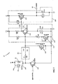
- the output circuit 20 is implemented by an amplifying circuit 210 connected to the cathode 10B of the buzzer 10 for amplifying the buzzer signal and a shaping circuit 220 for subsequently shaping the amplified buzzer signal to a logic (high) signal.
- the original buzzer signal is typically of a frequency of say 5kHz and a duration of about 2.2ms, having an amplitude that exceeds 0.35V for recognition or detection by the output circuit 20.
- the amplifying circuit 210 incorporates an NPN transistor 211 (Q6) as the main active element, whose base, collector and emitter are connected with first and second resistors R28 and R30 to 2.1V and a third resistor R31 in parallel with a capacitor C25 to the earth respectively as shown. Included is a second NPN transistor 212 (Q6') connected to act as a diode in series with a variable resistor R29 from the base of the main transistor 211 to the earth for temperature compensation. A further NPN transistor 203 is connected to act as a reversely-biased diode from the base of the main transistor 211 to the earth for protection against reverse biasing.
- the base of the main transistor 211 is connected to the cathode 10B of the buzzer 10 by means of a coupling circuit 201 formed by a resistor R22 and capacitor C23 connected in series for impedance/voltage matching.
- the collector of the transistor 211 outputs the amplified buzzer signal via a capacitor C24 to the shaping circuit 220.
- the shaping circuit 220 is implemented by a PNP transistor 221 (Q13'), whose base inputs the amplified buzzer signal.
- the emitter and base of the transistor 221 are connected directly and via a resistor R33 to 3V respectively, and its collector is connected via a resistor R34 in parallel with a capacitor C27 to the earth.
- the collector acts as an output terminal 21 of the overall output circuit 20 and provides a logic high (3V) signal (for the MCU 300) upon conduction of the transistor 221 as triggered by the buzzer signal generated by the buzzer 10 and boosted by the amplifying circuit 210.
- FIGS 3 and 4 show a first electronic device i.e. the sports watch 400 incorporating the subject tap-on switch device 100, which has a plastic watch case 410 having four control keys 401 and connected with a pair of plastic straps 413.
- the watch case 410 includes a plastic front lens 411 and is closed by a metal back cover 412, housing therein an LCD display 420 mounted on a printed circuit board 430 which carries the electronic operating circuit including the MCU 300 and also the output circuit 20 of the switch device 100.
- the buzzer 10 is located inside the watch case 410 and is fixed thereto such that any shock that is applied to the case 410 will reach or be received by the buzzer 10. More specifically, the buzzer base disc 12 is located flat against the inner surface of the back cover 412 and is secured firmly thereto by gel or glue for example.
- the buzzer anode 10A (i.e. the base disc 12) and cathode 10B (i.e. the piezoelectric ceramics 11) are electrically connected to the circuit board 430 by respective contact springs 431 and 432 that extend through the circuit components as shown. By means of the spring 432, the buzzer output i.e. the cathode 10B is connected via the output circuit 20 to the MCU 300.
- the sports watch 400 is used as a wristwatch for timekeeping including timer and alarm functions, etc. and also as a heart rate monitor for measuring and calculating the heart rate and related sports data. These functions are performed by or under the control of the MCU 300.
- the tap-on switch device 100 is installed completely inside the watch case 410 and is used to trigger the MCU 300 to perform a specific function that can be chosen from a number of predetermined functions, such as switching the mode of operation from time mode to heart rate mode (F1), acting as a snooze button (F2) for temporarily inhibiting an alarm (F2), or acting as a start/stop button for stop watch function.
- a specific function can be chosen from a number of predetermined functions, such as switching the mode of operation from time mode to heart rate mode (F1), acting as a snooze button (F2) for temporarily inhibiting an alarm (F2), or acting as a start/stop button for stop watch function.
- a user simply following manual (or on-screen) instructions can program or assign, for example by using the keys 401 of the watch 400, one of those functions to the switch device 100 such that the switch device 100 may be used to execute that function to meet his/her personal need or preference.
- the shock or vibration resulting from the tapping is transmitted via the body of the watch case 410 to reach the back cover 412 and hence the buzzer 10 in firm contact therewith.
- the buzzer 10 outputs a voltage signal by piezoelectric action, which is fed by the springs 431 to the output circuit 20 and 432 for amplification and then shaping into a logic high signal for triggering the MCU 300 to execute the programmed function, for example switching from time mode to heart rate mode (F1).
- Figure 5 shows a second electronic device i.e. the alarm clock 500 utilizing the same shock-activated/tap-on switch device 100, which has a plastic casing 510, an LCD display 520 and five control keys 501.
- the electronic operating circuit including the MCU 300 and the output circuit 20 of the switch device 100 are mounted on a printed circuit board located in the casing 510.
- the buzzer 10 is attached/mounted directly and firmly against the inner surface of the front or rear wall of the casing 510 by glue for example, such that detection by the buzzer 10 of tapping on the casing 510 is more effective.
- the operation is essentially the same.
- the shock or vibration caused by the tapping is transmitted via the body of the casing 510 to reach the buzzer 10, which upon vibration outputs a voltage signal by piezoelectric action, and the signal is amplified and shaped by the output circuit 20 to trigger the MCU 300 to execute the programmed function, for example to snooze an alarm (F2).
- Implementation of the subject shock-activated switch device is based on a piezoelectric element or buzzer which inherently exists in most electronic devices that are required to make a sound in use, for example to generate a beep alert message.
- the switch device utilizes the readily available or otherwise wasted reversed piezoelectric action of the buzzer, without incurring much extra cost (say, only for a few transistors and resistors). No special or complicate vibration/shock sensor is needed.
- the switch device is extremely easy and convenient to operate, even in the dark or when the user is occupied e.g. doing exercise, by simply tapping (or patting, knocking etc.) the casing/housing or body of the electronic device in which the switch device is used.
- the advantages achieved are certainly well worth the small extra cost in production.
Abstract
Description
- The present invention relates to a shock-activated switch device for controlling an electronic device.
- Electronic devices normally have several buttons or keys to operate various functions, and more features usually require the use of either more buttons or combination of buttons.
- For these products, there are often one or two popular functions that are frequently used. Most products would provide one large single function button for users' ease of access. For example, most heart rate monitor watches often include a big "quick-start" button which, upon pressing, will immediately switch the watch from the time mode to the heart rate measuring mode. Alarm clocks are another example, on which there is often a big snooze button for temporarily stopping the alarm beeps.
- However, conflict may arise when there are more than one popular feature in an electronic device, and individual users may have different preference of the feature they need most. It is obviously not feasible that every feature is served by a dedicated button. The provision of a large button in some cases is difficult if not impossible, for example on a wristwatch. In certain situations, whilst a specific button has been assigned to perform a certain function, the button may be difficult to locate or press especially in a dark environment or when the user is occupied for example doing exercise.
- An example of the prior art can be found in
United States Patent No. 5,946,274 , in which there is disclosed a shock switch and a posture detecting switch that are combined into an electronic device to perform an automatic operation such as turning on of the backlight of a wristwatch. One of the disadvantages of this design is that putting so many components into a small electronic device like a wristwatch is relatively complex and expensive. - The invention seeks to obviate or at least alleviate such a problem or shortcoming by providing a novel or otherwise improved shock-activated switch device.
- According to a first aspect of the invention, there is provided a shock-activated switch device comprising a piezoelectric element having a body for receiving a mechanical shock and a terminal for outputting an electrical output signal upon the body receiving a shock, and an output circuit connected to the terminal for converting said output signal into a logic signal for controlling an electronic circuit.
- Preferably, the piezoelectric element is capable of producing a sound upon application of an electrical signal at its terminal.
- More preferably, the piezoelectric element comprises a piezoelectric buzzer.
- It is preferred that the output circuit comprises an amplifying circuit for amplifying said output signal and a shaping circuit for subsequently shaping said output signal.
- According to a second aspect of the invention, there is provided an electronic device incorporating the shock-activated switch device as claimed in claim 1, further comprising a casing and an operating circuit including a control unit in the casing, in that the body of the piezoelectric element is located in fixed relationship to the casing for receiving said shock applied to the casing, and the terminal of the piezoelectric element is connected to provide said output signal to the control unit for causing the control unit to perform a specific function.
- Preferably, the body of the piezoelectric element is fixed firmly to the casing for vibration therewith.
- More preferably, the body of the piezoelectric element comprises a planar base which is located flat against an inner surface of the casing.
- In a preferred embodiment, the control unit is capable of performing at least two functions in response to said output signal from the terminal of the piezoelectric element, and includes selection means to enable user selection of one of these functions for execution.
- It is preferred that the piezoelectric element is connected to the operating circuit for operation thereby to provide an audio signal.
- Preferably, the electronic device is a sports watch.
- Preferably, the electronic device is an alarm clock.
- The invention will now be more particularly described, by way of example only, with reference to the accompanying drawings, in which:
- Figure 1 is a functional block diagram of an embodiment of a shock-activated switch device in accordance with the invention;
- Figure 2 is a detailed circuit diagram of the switch device of Figure 1;
- Figure 3 is a schematic front view of a first electronic device incorporating the switch device of Figure 1;
- Figure 4 is a schematic side view of the electronic device of Figure 3 worn on a wrist; and
- Figure 5 is a schematic front view of a second electronic device incorporating the switch device of Figure 1.
- Referring initially to Figures 1 to 4 of the drawings, there is shown a shock-activated or tap-on
switch device 100 embodying the invention, which comprises apiezoelectric element 10 and anoutput circuit 20 therefor. Thepiezoelectric element 10 is implemented conveniently by apiezoelectric buzzer 10 which is made of piezoelectric crystals orceramics 11 adhered on a planarcopper base disc 12, together constituting a body 13 that may experience or receive a mechanical shock, impact or vibration caused by tapping for example. - The
base disc 12 and the outer surface of thepiezoelectric ceramics 11 serve as the positive and negative terminals of thebuzzer 10, i.e.anode 10A andcathode 10B respectively. Upon application of an AC voltage across theterminals piezoelectric ceramics 11 will change shape by a small amount to thereby produce a sound. In the reversed operation, while theanode 10A is connected to a positive voltage source, thecathode 10B will output an electrical signal upon thepiezoelectric ceramics 11 or the buzzer body 13 in general being subjected to a shock or tapping. - The
buzzer 10 operates as a shock sensor or detector that provides an output signal (hereinafter referred to as the buzzer signal) upon activation by a small shock. With connection to thecathode 10B, theoutput circuit 20 is designed to convert the buzzer signal from an analogue signal into a logic high signal for controlling an MCU (microprocessor control unit) 300 of the operating circuit of an electronic device such as a sports watch 400 (Figures 3 and 4) or an alarm clock 500 (Figure 5). Thebuzzer 10 is preferably also in use for performing the more commonly known function i.e. emitting a sound as for example an alarm signal or key-press beep. - The
buzzer 10 is provided with ashunt coil 14, having itsanode 10A connected to 3V and itscathode 10B to the earth via the collector and emitter of anNPN transistor 202. Thetransistor 202 is part of the operating circuit that implements the general operation of the electronic device. Its base acts as an input for receiving a beep control signal to switch thetransistor 202 at a frequency of say 2kHz to 4kHz, thereby driving thebuzzer 10 to produce a beep sound. - The
output circuit 20 is implemented by an amplifyingcircuit 210 connected to thecathode 10B of thebuzzer 10 for amplifying the buzzer signal and a shaping circuit 220 for subsequently shaping the amplified buzzer signal to a logic (high) signal. The original buzzer signal is typically of a frequency of say 5kHz and a duration of about 2.2ms, having an amplitude that exceeds 0.35V for recognition or detection by theoutput circuit 20. - The amplifying
circuit 210 incorporates an NPN transistor 211 (Q6) as the main active element, whose base, collector and emitter are connected with first and second resistors R28 and R30 to 2.1V and a third resistor R31 in parallel with a capacitor C25 to the earth respectively as shown. Included is a second NPN transistor 212 (Q6') connected to act as a diode in series with a variable resistor R29 from the base of themain transistor 211 to the earth for temperature compensation. Afurther NPN transistor 203 is connected to act as a reversely-biased diode from the base of themain transistor 211 to the earth for protection against reverse biasing. - The base of the
main transistor 211 is connected to thecathode 10B of thebuzzer 10 by means of acoupling circuit 201 formed by a resistor R22 and capacitor C23 connected in series for impedance/voltage matching. The collector of thetransistor 211 outputs the amplified buzzer signal via a capacitor C24 to the shaping circuit 220. - The shaping circuit 220 is implemented by a PNP transistor 221 (Q13'), whose base inputs the amplified buzzer signal. The emitter and base of the
transistor 221 are connected directly and via a resistor R33 to 3V respectively, and its collector is connected via a resistor R34 in parallel with a capacitor C27 to the earth. The collector acts as anoutput terminal 21 of theoverall output circuit 20 and provides a logic high (3V) signal (for the MCU 300) upon conduction of thetransistor 221 as triggered by the buzzer signal generated by thebuzzer 10 and boosted by the amplifyingcircuit 210. - Figures 3 and 4 show a first electronic device i.e. the sports watch 400 incorporating the subject tap-on
switch device 100, which has aplastic watch case 410 having fourcontrol keys 401 and connected with a pair ofplastic straps 413. Thewatch case 410 includes aplastic front lens 411 and is closed by ametal back cover 412, housing therein anLCD display 420 mounted on a printedcircuit board 430 which carries the electronic operating circuit including theMCU 300 and also theoutput circuit 20 of theswitch device 100. - The
buzzer 10 is located inside thewatch case 410 and is fixed thereto such that any shock that is applied to thecase 410 will reach or be received by thebuzzer 10. More specifically, thebuzzer base disc 12 is located flat against the inner surface of theback cover 412 and is secured firmly thereto by gel or glue for example. Thebuzzer anode 10A (i.e. the base disc 12) andcathode 10B (i.e. the piezoelectric ceramics 11) are electrically connected to thecircuit board 430 byrespective contact springs spring 432, the buzzer output i.e. thecathode 10B is connected via theoutput circuit 20 to the MCU 300. - The
sports watch 400 is used as a wristwatch for timekeeping including timer and alarm functions, etc. and also as a heart rate monitor for measuring and calculating the heart rate and related sports data. These functions are performed by or under the control of theMCU 300. - The tap-on
switch device 100 is installed completely inside thewatch case 410 and is used to trigger theMCU 300 to perform a specific function that can be chosen from a number of predetermined functions, such as switching the mode of operation from time mode to heart rate mode (F1), acting as a snooze button (F2) for temporarily inhibiting an alarm (F2), or acting as a start/stop button for stop watch function. A user simply following manual (or on-screen) instructions can program or assign, for example by using thekeys 401 of thewatch 400, one of those functions to theswitch device 100 such that theswitch device 100 may be used to execute that function to meet his/her personal need or preference. - In operation, upon the user tapping on the
watch case 410, for example on thewatch lens 411, the shock or vibration resulting from the tapping is transmitted via the body of thewatch case 410 to reach theback cover 412 and hence thebuzzer 10 in firm contact therewith. Upon vibration, thebuzzer 10 outputs a voltage signal by piezoelectric action, which is fed by thesprings 431 to theoutput circuit MCU 300 to execute the programmed function, for example switching from time mode to heart rate mode (F1). - Figure 5 shows a second electronic device i.e. the
alarm clock 500 utilizing the same shock-activated/tap-onswitch device 100, which has aplastic casing 510, anLCD display 520 and fivecontrol keys 501. The electronic operating circuit including theMCU 300 and theoutput circuit 20 of theswitch device 100 are mounted on a printed circuit board located in thecasing 510. Thebuzzer 10 is attached/mounted directly and firmly against the inner surface of the front or rear wall of thecasing 510 by glue for example, such that detection by thebuzzer 10 of tapping on thecasing 510 is more effective. - The operation is essentially the same. Upon the user tapping on the
clock casing 510, the shock or vibration caused by the tapping is transmitted via the body of thecasing 510 to reach thebuzzer 10, which upon vibration outputs a voltage signal by piezoelectric action, and the signal is amplified and shaped by theoutput circuit 20 to trigger theMCU 300 to execute the programmed function, for example to snooze an alarm (F2). - Implementation of the subject shock-activated switch device is based on a piezoelectric element or buzzer which inherently exists in most electronic devices that are required to make a sound in use, for example to generate a beep alert message. The switch device utilizes the readily available or otherwise wasted reversed piezoelectric action of the buzzer, without incurring much extra cost (say, only for a few transistors and resistors). No special or complicate vibration/shock sensor is needed.
- The switch device is extremely easy and convenient to operate, even in the dark or when the user is occupied e.g. doing exercise, by simply tapping (or patting, knocking etc.) the casing/housing or body of the electronic device in which the switch device is used. The advantages achieved are certainly well worth the small extra cost in production.
- The invention has been given by way of example only, and various modifications of and/or alterations to the described embodiments may be made by persons skilled in the art without departing from the scope of the invention as specified in the appended claims.
Claims (11)
- A shock-activated switch device comprising:a piezoelectric element having a body for receiving a mechanical shock and a terminal for outputting an electrical output signal upon the body receiving a shock; andan output circuit connected to the terminal for converting said output signal into a logic signal for controlling an electronic circuit.
- The shock-activated switch device as claimed in claim 1, characterized in that the piezoelectric element is capable of producing a sound upon application of an electrical signal at its terminal.
- The shock-activated switch device as claimed in claim 2, characterized in that the piezoelectric element comprises a piezoelectric buzzer.
- The shock-activated switch device as claimed in claim 1, characterized in that the output circuit comprises an amplifying circuit for amplifying said output signal and a shaping circuit for subsequently shaping said output signal.
- An electronic device incorporating the shock-activated switch device as claimed in any one of claims 1 to 4, further comprising a casing and an operating circuit including a control unit in the casing, characterized in that the body of the piezoelectric element is located in fixed relationship to the casing for receiving said shock applied to the casing, and the terminal of the piezoelectric element is connected to provide said output signal to the control unit for causing the control unit to perform a specific function.
- The electronic device as claimed in claim 5, characterized in that the body of the piezoelectric element is fixed firmly to the casing for vibration therewith.
- The electronic device as claimed in claim 6, characterized in that the body of the piezoelectric element comprises a planar base which is located flat against an inner surface of the casing.
- The electronic device as claimed in claim 5, characterized in that the control unit is capable of performing at least two functions in response to said output signal from the terminal of the piezoelectric element, and includes selection means to enable user selection of one of these functions for execution.
- The electronic device as claimed in claim 5, characterized in that the piezoelectric element is connected to the operating circuit for operation thereby to provide an audio signal.
- The electronic device as claimed in claim 5, characterized in being a sports watch.
- The electronic device as claimed in claim 5, characterized in being an alarm clock.
Applications Claiming Priority (1)
| Application Number | Priority Date | Filing Date | Title |
|---|---|---|---|
| US11/372,347 US7817500B2 (en) | 2006-03-10 | 2006-03-10 | Shock-activated switch device |
Publications (2)
| Publication Number | Publication Date |
|---|---|
| EP1833103A1 true EP1833103A1 (en) | 2007-09-12 |
| EP1833103B1 EP1833103B1 (en) | 2011-09-07 |
Family
ID=38043036
Family Applications (1)
| Application Number | Title | Priority Date | Filing Date |
|---|---|---|---|
| EP07250895A Not-in-force EP1833103B1 (en) | 2006-03-10 | 2007-03-02 | Shock-activated switch device |
Country Status (6)
| Country | Link |
|---|---|
| US (1) | US7817500B2 (en) |
| EP (1) | EP1833103B1 (en) |
| CN (1) | CN101034889B (en) |
| AT (1) | ATE523903T1 (en) |
| ES (1) | ES2372588T3 (en) |
| HK (1) | HK1101937A1 (en) |
Cited By (7)
| Publication number | Priority date | Publication date | Assignee | Title |
|---|---|---|---|---|
| WO2010126825A1 (en) * | 2009-04-26 | 2010-11-04 | Nike International, Ltd. | Athletic watch |
| WO2012020356A1 (en) | 2010-08-12 | 2012-02-16 | Koninklijke Philips Electronics N.V. | Tap sensitive alarm clock |
| JP2014209092A (en) * | 2013-03-27 | 2014-11-06 | セイコーインスツル株式会社 | Electronic apparatus and impact detection method |
| US9141087B2 (en) | 2009-04-26 | 2015-09-22 | Nike, Inc. | Athletic watch |
| US9269102B2 (en) | 2009-05-21 | 2016-02-23 | Nike, Inc. | Collaborative activities in on-line commerce |
| WO2016178581A1 (en) * | 2015-05-04 | 2016-11-10 | Sunsense As | A compact ultraviolet light radiation sensing device |
| US10069059B2 (en) | 2016-05-12 | 2018-09-04 | Inventus Power | Method and apparatus for shake awake smart battery pack |
Families Citing this family (7)
| Publication number | Priority date | Publication date | Assignee | Title |
|---|---|---|---|---|
| US8036068B1 (en) * | 2010-05-03 | 2011-10-11 | Sony Corporation | Digital alarm clock with user-selectable alarm sound source including from internet |
| CN102176670A (en) * | 2010-12-23 | 2011-09-07 | 王存 | Wire-connection-free electric switch |
| CN105391341B (en) | 2014-09-01 | 2017-09-01 | 三星电机株式会社 | Piezoelectric energy collector and the wireless switching for including the piezoelectric energy collector |
| US9876445B2 (en) | 2014-09-01 | 2018-01-23 | Samsung Electro-Mechanics Co., Ltd. | Piezoelectric energy harvester and wireless switch including the same |
| TWI541621B (en) * | 2014-09-15 | 2016-07-11 | 神達電腦股份有限公司 | Watch and method for automatically turning on a backlight |
| CN105448007B (en) * | 2015-11-11 | 2017-11-07 | 东方通信股份有限公司 | Buzzer vibration alarming module |
| CN105595978A (en) * | 2016-03-15 | 2016-05-25 | 中山大学 | Old-person home-old-aged-caring monitoring system and method based on indoor positioning |
Citations (5)
| Publication number | Priority date | Publication date | Assignee | Title |
|---|---|---|---|---|
| US688A (en) | 1838-04-13 | james | ||
| US5977A (en) | 1848-12-19 | Joseph p | ||
| GB2262988A (en) * | 1992-01-02 | 1993-07-07 | James R Adams & Associates Ltd | Manually operated device for illuminating wrist-watch or instrument displays. |
| US5946274A (en) | 1996-12-11 | 1999-08-31 | Casio Computer Co., Ltd. | Switch device and electronic device which includes such switch device |
| US5977688A (en) * | 1997-03-28 | 1999-11-02 | Seiko Instruments R & D Center Inc. | Electronic apparatus for being switched using piezoelectric element |
Family Cites Families (9)
| Publication number | Priority date | Publication date | Assignee | Title |
|---|---|---|---|---|
| CH616816B (en) * | 1975-10-08 | 1900-01-01 | Suwa Seikosha Kk | ELECTRONIC WRISTWATCH. |
| CH621460B (en) * | 1977-12-23 | Ebauches Electroniques Sa | ELECTRONIC WATCHMAKING PART WITH ELECTROACOUSTIC TRANSDUCER. | |
| CH654169GA3 (en) * | 1984-04-25 | 1986-02-14 | ||
| US4761582A (en) * | 1987-03-19 | 1988-08-02 | Motorola, Inc. | Dual mode transducer |
| US5783875A (en) * | 1997-02-11 | 1998-07-21 | The Lamson & Sessions Co. | Touch sensor circuit |
| ATE343267T1 (en) * | 1999-08-03 | 2006-11-15 | Eta Sa Mft Horlogere Suisse | ELECTRONIC CONVERTER OF AN ACOUSTIC SIGNAL INTO A PSEUDO-DIGITAL SIGNAL AND BIDIRECTIONAL COMMUNICATION METHOD THROUGH SOUND WAVES |
| SG97904A1 (en) * | 1999-08-04 | 2003-08-20 | Ebauchesfabrik Eta Ag | Electronic converter for converting an acoustic signal into a pseudodigital signal, timepiece including such a converter and two-directional communications method via acoustic waves |
| SG96198A1 (en) * | 2000-02-24 | 2003-05-23 | Asulab Sa | Portable object such as, in particular, a timepiece, including a piezoelectric transducer for entering data manually |
| US20040164647A1 (en) * | 2003-02-26 | 2004-08-26 | Micko Eric Scott | Piezoelectric transducer circuit with improved shock recovery |
-
2006
- 2006-03-10 US US11/372,347 patent/US7817500B2/en not_active Expired - Fee Related
-
2007
- 2007-03-02 ES ES07250895T patent/ES2372588T3/en active Active
- 2007-03-02 AT AT07250895T patent/ATE523903T1/en not_active IP Right Cessation
- 2007-03-02 EP EP07250895A patent/EP1833103B1/en not_active Not-in-force
- 2007-03-12 CN CN200710085577.7A patent/CN101034889B/en not_active Expired - Fee Related
- 2007-09-13 HK HK07109957.5A patent/HK1101937A1/en not_active IP Right Cessation
Patent Citations (5)
| Publication number | Priority date | Publication date | Assignee | Title |
|---|---|---|---|---|
| US688A (en) | 1838-04-13 | james | ||
| US5977A (en) | 1848-12-19 | Joseph p | ||
| GB2262988A (en) * | 1992-01-02 | 1993-07-07 | James R Adams & Associates Ltd | Manually operated device for illuminating wrist-watch or instrument displays. |
| US5946274A (en) | 1996-12-11 | 1999-08-31 | Casio Computer Co., Ltd. | Switch device and electronic device which includes such switch device |
| US5977688A (en) * | 1997-03-28 | 1999-11-02 | Seiko Instruments R & D Center Inc. | Electronic apparatus for being switched using piezoelectric element |
Cited By (29)
| Publication number | Priority date | Publication date | Assignee | Title |
|---|---|---|---|---|
| US9891596B2 (en) | 2009-04-26 | 2018-02-13 | Nike, Inc. | Athletic watch |
| US9141087B2 (en) | 2009-04-26 | 2015-09-22 | Nike, Inc. | Athletic watch |
| EP2581120A1 (en) * | 2009-04-26 | 2013-04-17 | Nike International Ltd. | Athletic watch |
| EP2584414A1 (en) * | 2009-04-26 | 2013-04-24 | Nike International Ltd. | Athletic Watch |
| US8562489B2 (en) | 2009-04-26 | 2013-10-22 | Nike, Inc. | Athletic watch |
| US11092459B2 (en) | 2009-04-26 | 2021-08-17 | Nike, Inc. | GPS features and functionality in an athletic watch system |
| US9977405B2 (en) | 2009-04-26 | 2018-05-22 | Nike, Inc. | Athletic watch |
| US9122250B2 (en) | 2009-04-26 | 2015-09-01 | Nike, Inc. | GPS features and functionality in an athletic watch system |
| US9785121B2 (en) | 2009-04-26 | 2017-10-10 | Nike, Inc. | Athletic watch |
| US10824118B2 (en) | 2009-04-26 | 2020-11-03 | Nike, Inc. | Athletic watch |
| WO2010126825A1 (en) * | 2009-04-26 | 2010-11-04 | Nike International, Ltd. | Athletic watch |
| US9864342B2 (en) | 2009-04-26 | 2018-01-09 | Nike, Inc. | Athletic watch |
| US9329053B2 (en) | 2009-04-26 | 2016-05-03 | Nike, Inc. | Athletic watch |
| US10564002B2 (en) | 2009-04-26 | 2020-02-18 | Nike, Inc. | GPS features and functionality in an athletic watch system |
| US10429204B2 (en) | 2009-04-26 | 2019-10-01 | Nike, Inc. | GPS features and functionality in an athletic watch system |
| US9269102B2 (en) | 2009-05-21 | 2016-02-23 | Nike, Inc. | Collaborative activities in on-line commerce |
| US9704187B2 (en) | 2009-05-21 | 2017-07-11 | Nike, Inc. | Collaborative activities in on-line commerce |
| US10664882B2 (en) | 2009-05-21 | 2020-05-26 | Nike, Inc. | Collaborative activities in on-line commerce |
| US10997642B2 (en) | 2009-05-21 | 2021-05-04 | Nike, Inc. | Collaborative activities in on-line commerce |
| US11741515B2 (en) | 2009-05-21 | 2023-08-29 | Nike, Inc. | Collaborative activities in on-line commerce |
| US10317849B2 (en) | 2010-08-12 | 2019-06-11 | Koninklijke Philips N.V. | Tap sensitive alarm clock |
| RU2568940C2 (en) * | 2010-08-12 | 2015-11-20 | Конинклейке Филипс Электроникс Н.В. | Touch-sensitive alarm clock |
| US8908478B2 (en) | 2010-08-12 | 2014-12-09 | Koninklijke Philips N.V. | Tap sensitive alarm clock |
| WO2012020356A1 (en) | 2010-08-12 | 2012-02-16 | Koninklijke Philips Electronics N.V. | Tap sensitive alarm clock |
| US9546919B2 (en) | 2013-03-27 | 2017-01-17 | Seiko Instruments Inc. | Electronic apparatus and shock detection method |
| EP2784604A3 (en) * | 2013-03-27 | 2016-02-24 | Seiko Instruments Inc. | Electronic apparatus and shock detection method |
| JP2014209092A (en) * | 2013-03-27 | 2014-11-06 | セイコーインスツル株式会社 | Electronic apparatus and impact detection method |
| WO2016178581A1 (en) * | 2015-05-04 | 2016-11-10 | Sunsense As | A compact ultraviolet light radiation sensing device |
| US10069059B2 (en) | 2016-05-12 | 2018-09-04 | Inventus Power | Method and apparatus for shake awake smart battery pack |
Also Published As
| Publication number | Publication date |
|---|---|
| ES2372588T3 (en) | 2012-01-24 |
| ATE523903T1 (en) | 2011-09-15 |
| HK1101937A1 (en) | 2007-11-02 |
| CN101034889A (en) | 2007-09-12 |
| US20070211577A1 (en) | 2007-09-13 |
| EP1833103B1 (en) | 2011-09-07 |
| US7817500B2 (en) | 2010-10-19 |
| CN101034889B (en) | 2012-05-09 |
Similar Documents
| Publication | Publication Date | Title |
|---|---|---|
| EP1833103B1 (en) | Shock-activated switch device | |
| JP4252754B2 (en) | Portable object including electronic function operating means and method for controlling the electronic function | |
| US6008720A (en) | Portable timer alarm device with ear attachment | |
| US7283039B2 (en) | Window-attached alerting device | |
| US4444515A (en) | Earring watch | |
| US5486818A (en) | Wireless switch for a telemetric receiver | |
| US20160011709A1 (en) | Portable electronic device for information display | |
| US20050249049A1 (en) | Personal safety device | |
| US6310428B1 (en) | Piezoelectric switch with audible feedback | |
| US6813223B1 (en) | Portable object such as, in particular, a timepiece, including a piezoelectric transducer for entering data manually | |
| US5977688A (en) | Electronic apparatus for being switched using piezoelectric element | |
| US9542816B1 (en) | Wearable alert device having selectable alert volume and method of operating same | |
| KR200342585Y1 (en) | Digital watch capable for displaying temperature | |
| JP2009099521A (en) | Tilted vibration sensor and portable apparatus using the same, and crime prevention system | |
| CN209992817U (en) | Electronic watch with hand-lifting cold light display | |
| JP3139467U (en) | Ear clock | |
| JPH0587952A (en) | Wristwatch with alarm function | |
| JP2952404B2 (en) | Electronics | |
| JP2005140744A (en) | Alarm clock | |
| KR880001874Y1 (en) | Telephone | |
| EP1367466A1 (en) | Time zone setting device | |
| JP2017173086A (en) | Electronic timepiece | |
| JPS61234386A (en) | Alarm timepiece | |
| JPS63137894U (en) | ||
| KR20090130483A (en) | Hand tremor clock |
Legal Events
| Date | Code | Title | Description |
|---|---|---|---|
| PUAI | Public reference made under article 153(3) epc to a published international application that has entered the european phase |
Free format text: ORIGINAL CODE: 0009012 |
|
| AK | Designated contracting states |
Kind code of ref document: A1 Designated state(s): AT BE BG CH CY CZ DE DK EE ES FI FR GB GR HU IE IS IT LI LT LU LV MC MT NL PL PT RO SE SI SK TR |
|
| AX | Request for extension of the european patent |
Extension state: AL BA HR MK YU |
|
| REG | Reference to a national code |
Ref country code: HK Ref legal event code: DE Ref document number: 1101937 Country of ref document: HK |
|
| 17P | Request for examination filed |
Effective date: 20080306 |
|
| 17Q | First examination report despatched |
Effective date: 20080404 |
|
| AKX | Designation fees paid |
Designated state(s): AT BE BG CH CY CZ DE DK EE ES FI FR GB GR HU IE IS IT LI LT LU LV MC MT NL PL PT RO SE SI SK TR |
|
| GRAP | Despatch of communication of intention to grant a patent |
Free format text: ORIGINAL CODE: EPIDOSNIGR1 |
|
| GRAS | Grant fee paid |
Free format text: ORIGINAL CODE: EPIDOSNIGR3 |
|
| GRAA | (expected) grant |
Free format text: ORIGINAL CODE: 0009210 |
|
| REG | Reference to a national code |
Ref country code: GB Ref legal event code: FG4D |
|
| REG | Reference to a national code |
Ref country code: CH Ref legal event code: EP |
|
| REG | Reference to a national code |
Ref country code: IE Ref legal event code: FG4D |
|
| REG | Reference to a national code |
Ref country code: DE Ref legal event code: R096 Ref document number: 602007016932 Country of ref document: DE Effective date: 20111103 |
|
| REG | Reference to a national code |
Ref country code: HK Ref legal event code: GR Ref document number: 1101937 Country of ref document: HK |
|
| REG | Reference to a national code |
Ref country code: NL Ref legal event code: T3 |
|
| REG | Reference to a national code |
Ref country code: ES Ref legal event code: FG2A Ref document number: 2372588 Country of ref document: ES Kind code of ref document: T3 Effective date: 20120124 |
|
| PG25 | Lapsed in a contracting state [announced via postgrant information from national office to epo] |
Ref country code: FI Free format text: LAPSE BECAUSE OF FAILURE TO SUBMIT A TRANSLATION OF THE DESCRIPTION OR TO PAY THE FEE WITHIN THE PRESCRIBED TIME-LIMIT Effective date: 20110907 Ref country code: LT Free format text: LAPSE BECAUSE OF FAILURE TO SUBMIT A TRANSLATION OF THE DESCRIPTION OR TO PAY THE FEE WITHIN THE PRESCRIBED TIME-LIMIT Effective date: 20110907 Ref country code: SE Free format text: LAPSE BECAUSE OF FAILURE TO SUBMIT A TRANSLATION OF THE DESCRIPTION OR TO PAY THE FEE WITHIN THE PRESCRIBED TIME-LIMIT Effective date: 20110907 |
|
| LTIE | Lt: invalidation of european patent or patent extension |
Effective date: 20110907 |
|
| PG25 | Lapsed in a contracting state [announced via postgrant information from national office to epo] |
Ref country code: AT Free format text: LAPSE BECAUSE OF FAILURE TO SUBMIT A TRANSLATION OF THE DESCRIPTION OR TO PAY THE FEE WITHIN THE PRESCRIBED TIME-LIMIT Effective date: 20110907 Ref country code: GR Free format text: LAPSE BECAUSE OF FAILURE TO SUBMIT A TRANSLATION OF THE DESCRIPTION OR TO PAY THE FEE WITHIN THE PRESCRIBED TIME-LIMIT Effective date: 20111208 Ref country code: CY Free format text: LAPSE BECAUSE OF FAILURE TO SUBMIT A TRANSLATION OF THE DESCRIPTION OR TO PAY THE FEE WITHIN THE PRESCRIBED TIME-LIMIT Effective date: 20110907 Ref country code: LV Free format text: LAPSE BECAUSE OF FAILURE TO SUBMIT A TRANSLATION OF THE DESCRIPTION OR TO PAY THE FEE WITHIN THE PRESCRIBED TIME-LIMIT Effective date: 20110907 Ref country code: SI Free format text: LAPSE BECAUSE OF FAILURE TO SUBMIT A TRANSLATION OF THE DESCRIPTION OR TO PAY THE FEE WITHIN THE PRESCRIBED TIME-LIMIT Effective date: 20110907 |
|
| REG | Reference to a national code |
Ref country code: AT Ref legal event code: MK05 Ref document number: 523903 Country of ref document: AT Kind code of ref document: T Effective date: 20110907 |
|
| PG25 | Lapsed in a contracting state [announced via postgrant information from national office to epo] |
Ref country code: BE Free format text: LAPSE BECAUSE OF FAILURE TO SUBMIT A TRANSLATION OF THE DESCRIPTION OR TO PAY THE FEE WITHIN THE PRESCRIBED TIME-LIMIT Effective date: 20110907 |
|
| PG25 | Lapsed in a contracting state [announced via postgrant information from national office to epo] |
Ref country code: CZ Free format text: LAPSE BECAUSE OF FAILURE TO SUBMIT A TRANSLATION OF THE DESCRIPTION OR TO PAY THE FEE WITHIN THE PRESCRIBED TIME-LIMIT Effective date: 20110907 Ref country code: IS Free format text: LAPSE BECAUSE OF FAILURE TO SUBMIT A TRANSLATION OF THE DESCRIPTION OR TO PAY THE FEE WITHIN THE PRESCRIBED TIME-LIMIT Effective date: 20120107 Ref country code: SK Free format text: LAPSE BECAUSE OF FAILURE TO SUBMIT A TRANSLATION OF THE DESCRIPTION OR TO PAY THE FEE WITHIN THE PRESCRIBED TIME-LIMIT Effective date: 20110907 |
|
| PG25 | Lapsed in a contracting state [announced via postgrant information from national office to epo] |
Ref country code: EE Free format text: LAPSE BECAUSE OF FAILURE TO SUBMIT A TRANSLATION OF THE DESCRIPTION OR TO PAY THE FEE WITHIN THE PRESCRIBED TIME-LIMIT Effective date: 20110907 Ref country code: RO Free format text: LAPSE BECAUSE OF FAILURE TO SUBMIT A TRANSLATION OF THE DESCRIPTION OR TO PAY THE FEE WITHIN THE PRESCRIBED TIME-LIMIT Effective date: 20110907 Ref country code: PT Free format text: LAPSE BECAUSE OF FAILURE TO SUBMIT A TRANSLATION OF THE DESCRIPTION OR TO PAY THE FEE WITHIN THE PRESCRIBED TIME-LIMIT Effective date: 20120109 Ref country code: PL Free format text: LAPSE BECAUSE OF FAILURE TO SUBMIT A TRANSLATION OF THE DESCRIPTION OR TO PAY THE FEE WITHIN THE PRESCRIBED TIME-LIMIT Effective date: 20110907 |
|
| PGFP | Annual fee paid to national office [announced via postgrant information from national office to epo] |
Ref country code: IT Payment date: 20120315 Year of fee payment: 6 |
|
| PLBE | No opposition filed within time limit |
Free format text: ORIGINAL CODE: 0009261 |
|
| STAA | Information on the status of an ep patent application or granted ep patent |
Free format text: STATUS: NO OPPOSITION FILED WITHIN TIME LIMIT |
|
| PG25 | Lapsed in a contracting state [announced via postgrant information from national office to epo] |
Ref country code: DK Free format text: LAPSE BECAUSE OF FAILURE TO SUBMIT A TRANSLATION OF THE DESCRIPTION OR TO PAY THE FEE WITHIN THE PRESCRIBED TIME-LIMIT Effective date: 20110907 |
|
| 26N | No opposition filed |
Effective date: 20120611 |
|
| REG | Reference to a national code |
Ref country code: DE Ref legal event code: R097 Ref document number: 602007016932 Country of ref document: DE Effective date: 20120611 |
|
| PG25 | Lapsed in a contracting state [announced via postgrant information from national office to epo] |
Ref country code: MC Free format text: LAPSE BECAUSE OF NON-PAYMENT OF DUE FEES Effective date: 20120331 |
|
| REG | Reference to a national code |
Ref country code: CH Ref legal event code: PL |
|
| REG | Reference to a national code |
Ref country code: IE Ref legal event code: MM4A |
|
| PG25 | Lapsed in a contracting state [announced via postgrant information from national office to epo] |
Ref country code: IE Free format text: LAPSE BECAUSE OF NON-PAYMENT OF DUE FEES Effective date: 20120302 Ref country code: CH Free format text: LAPSE BECAUSE OF NON-PAYMENT OF DUE FEES Effective date: 20120331 Ref country code: LI Free format text: LAPSE BECAUSE OF NON-PAYMENT OF DUE FEES Effective date: 20120331 |
|
| PGFP | Annual fee paid to national office [announced via postgrant information from national office to epo] |
Ref country code: ES Payment date: 20130313 Year of fee payment: 7 Ref country code: FR Payment date: 20130325 Year of fee payment: 7 Ref country code: DE Payment date: 20130227 Year of fee payment: 7 Ref country code: GB Payment date: 20130228 Year of fee payment: 7 |
|
| PGFP | Annual fee paid to national office [announced via postgrant information from national office to epo] |
Ref country code: NL Payment date: 20130309 Year of fee payment: 7 |
|
| PG25 | Lapsed in a contracting state [announced via postgrant information from national office to epo] |
Ref country code: BG Free format text: LAPSE BECAUSE OF FAILURE TO SUBMIT A TRANSLATION OF THE DESCRIPTION OR TO PAY THE FEE WITHIN THE PRESCRIBED TIME-LIMIT Effective date: 20111207 |
|
| PG25 | Lapsed in a contracting state [announced via postgrant information from national office to epo] |
Ref country code: MT Free format text: LAPSE BECAUSE OF FAILURE TO SUBMIT A TRANSLATION OF THE DESCRIPTION OR TO PAY THE FEE WITHIN THE PRESCRIBED TIME-LIMIT Effective date: 20110907 |
|
| PG25 | Lapsed in a contracting state [announced via postgrant information from national office to epo] |
Ref country code: TR Free format text: LAPSE BECAUSE OF FAILURE TO SUBMIT A TRANSLATION OF THE DESCRIPTION OR TO PAY THE FEE WITHIN THE PRESCRIBED TIME-LIMIT Effective date: 20110907 |
|
| PG25 | Lapsed in a contracting state [announced via postgrant information from national office to epo] |
Ref country code: LU Free format text: LAPSE BECAUSE OF NON-PAYMENT OF DUE FEES Effective date: 20120302 |
|
| PG25 | Lapsed in a contracting state [announced via postgrant information from national office to epo] |
Ref country code: HU Free format text: LAPSE BECAUSE OF FAILURE TO SUBMIT A TRANSLATION OF THE DESCRIPTION OR TO PAY THE FEE WITHIN THE PRESCRIBED TIME-LIMIT Effective date: 20070302 |
|
| REG | Reference to a national code |
Ref country code: DE Ref legal event code: R119 Ref document number: 602007016932 Country of ref document: DE |
|
| REG | Reference to a national code |
Ref country code: NL Ref legal event code: V1 Effective date: 20141001 |
|
| GBPC | Gb: european patent ceased through non-payment of renewal fee |
Effective date: 20140302 |
|
| REG | Reference to a national code |
Ref country code: FR Ref legal event code: ST Effective date: 20141128 |
|
| REG | Reference to a national code |
Ref country code: DE Ref legal event code: R119 Ref document number: 602007016932 Country of ref document: DE Effective date: 20141001 |
|
| PG25 | Lapsed in a contracting state [announced via postgrant information from national office to epo] |
Ref country code: DE Free format text: LAPSE BECAUSE OF NON-PAYMENT OF DUE FEES Effective date: 20141001 Ref country code: FR Free format text: LAPSE BECAUSE OF NON-PAYMENT OF DUE FEES Effective date: 20140331 Ref country code: GB Free format text: LAPSE BECAUSE OF NON-PAYMENT OF DUE FEES Effective date: 20140302 |
|
| PG25 | Lapsed in a contracting state [announced via postgrant information from national office to epo] |
Ref country code: NL Free format text: LAPSE BECAUSE OF NON-PAYMENT OF DUE FEES Effective date: 20141001 |
|
| PG25 | Lapsed in a contracting state [announced via postgrant information from national office to epo] |
Ref country code: IT Free format text: LAPSE BECAUSE OF NON-PAYMENT OF DUE FEES Effective date: 20140302 |
|
| PG25 | Lapsed in a contracting state [announced via postgrant information from national office to epo] |
Ref country code: ES Free format text: LAPSE BECAUSE OF NON-PAYMENT OF DUE FEES Effective date: 20140303 |