EP1808901A2 - Semiconductor sensor using surface plasmons to increase energy absorption efficiency - Google Patents
Semiconductor sensor using surface plasmons to increase energy absorption efficiency Download PDFInfo
- Publication number
- EP1808901A2 EP1808901A2 EP06013963A EP06013963A EP1808901A2 EP 1808901 A2 EP1808901 A2 EP 1808901A2 EP 06013963 A EP06013963 A EP 06013963A EP 06013963 A EP06013963 A EP 06013963A EP 1808901 A2 EP1808901 A2 EP 1808901A2
- Authority
- EP
- European Patent Office
- Prior art keywords
- semiconductor layer
- corrugated
- incident
- semiconductor
- interface
- Prior art date
- Legal status (The legal status is an assumption and is not a legal conclusion. Google has not performed a legal analysis and makes no representation as to the accuracy of the status listed.)
- Withdrawn
Links
- 239000004065 semiconductor Substances 0.000 title claims abstract description 56
- 238000010521 absorption reaction Methods 0.000 title claims abstract description 10
- 239000002184 metal Substances 0.000 claims abstract description 45
- 229910052751 metal Inorganic materials 0.000 claims abstract description 45
- XUIMIQQOPSSXEZ-UHFFFAOYSA-N Silicon Chemical compound [Si] XUIMIQQOPSSXEZ-UHFFFAOYSA-N 0.000 claims description 46
- 229910052710 silicon Inorganic materials 0.000 claims description 46
- 239000010703 silicon Substances 0.000 claims description 46
- 230000008878 coupling Effects 0.000 description 12
- 238000010168 coupling process Methods 0.000 description 12
- 238000005859 coupling reaction Methods 0.000 description 12
- 239000006185 dispersion Substances 0.000 description 9
- 238000001228 spectrum Methods 0.000 description 6
- 238000010586 diagram Methods 0.000 description 5
- 239000000463 material Substances 0.000 description 5
- 230000005684 electric field Effects 0.000 description 4
- 230000001902 propagating effect Effects 0.000 description 4
- 230000003287 optical effect Effects 0.000 description 3
- VYPSYNLAJGMNEJ-UHFFFAOYSA-N Silicium dioxide Chemical compound O=[Si]=O VYPSYNLAJGMNEJ-UHFFFAOYSA-N 0.000 description 2
- 230000000694 effects Effects 0.000 description 2
- 230000004048 modification Effects 0.000 description 2
- 238000012986 modification Methods 0.000 description 2
- 229910005540 GaP Inorganic materials 0.000 description 1
- 229910005542 GaSb Inorganic materials 0.000 description 1
- 229910001218 Gallium arsenide Inorganic materials 0.000 description 1
- 229910000673 Indium arsenide Inorganic materials 0.000 description 1
- GPXJNWSHGFTCBW-UHFFFAOYSA-N Indium phosphide Chemical compound [In]#P GPXJNWSHGFTCBW-UHFFFAOYSA-N 0.000 description 1
- 229910052782 aluminium Inorganic materials 0.000 description 1
- 230000002238 attenuated effect Effects 0.000 description 1
- 238000005452 bending Methods 0.000 description 1
- UHYPYGJEEGLRJD-UHFFFAOYSA-N cadmium(2+);selenium(2-) Chemical compound [Se-2].[Cd+2] UHYPYGJEEGLRJD-UHFFFAOYSA-N 0.000 description 1
- 229910052681 coesite Inorganic materials 0.000 description 1
- 239000004020 conductor Substances 0.000 description 1
- 229910052906 cristobalite Inorganic materials 0.000 description 1
- 230000007423 decrease Effects 0.000 description 1
- 239000003989 dielectric material Substances 0.000 description 1
- 230000005672 electromagnetic field Effects 0.000 description 1
- 238000005516 engineering process Methods 0.000 description 1
- 230000014509 gene expression Effects 0.000 description 1
- 229910052737 gold Inorganic materials 0.000 description 1
- 238000003384 imaging method Methods 0.000 description 1
- 239000012535 impurity Substances 0.000 description 1
- WPYVAWXEWQSOGY-UHFFFAOYSA-N indium antimonide Chemical compound [Sb]#[In] WPYVAWXEWQSOGY-UHFFFAOYSA-N 0.000 description 1
- RPQDHPTXJYYUPQ-UHFFFAOYSA-N indium arsenide Chemical compound [In]#[As] RPQDHPTXJYYUPQ-UHFFFAOYSA-N 0.000 description 1
- 239000012212 insulator Substances 0.000 description 1
- 229910052759 nickel Inorganic materials 0.000 description 1
- 230000010355 oscillation Effects 0.000 description 1
- 239000000377 silicon dioxide Substances 0.000 description 1
- 229910052709 silver Inorganic materials 0.000 description 1
- 229910052682 stishovite Inorganic materials 0.000 description 1
- 229910052905 tridymite Inorganic materials 0.000 description 1
Images


Classifications
-
- H—ELECTRICITY
- H01—ELECTRIC ELEMENTS
- H01L—SEMICONDUCTOR DEVICES NOT COVERED BY CLASS H10
- H01L31/00—Semiconductor devices sensitive to infrared radiation, light, electromagnetic radiation of shorter wavelength or corpuscular radiation and specially adapted either for the conversion of the energy of such radiation into electrical energy or for the control of electrical energy by such radiation; Processes or apparatus specially adapted for the manufacture or treatment thereof or of parts thereof; Details thereof
- H01L31/0248—Semiconductor devices sensitive to infrared radiation, light, electromagnetic radiation of shorter wavelength or corpuscular radiation and specially adapted either for the conversion of the energy of such radiation into electrical energy or for the control of electrical energy by such radiation; Processes or apparatus specially adapted for the manufacture or treatment thereof or of parts thereof; Details thereof characterised by their semiconductor bodies
- H01L31/0352—Semiconductor devices sensitive to infrared radiation, light, electromagnetic radiation of shorter wavelength or corpuscular radiation and specially adapted either for the conversion of the energy of such radiation into electrical energy or for the control of electrical energy by such radiation; Processes or apparatus specially adapted for the manufacture or treatment thereof or of parts thereof; Details thereof characterised by their semiconductor bodies characterised by their shape or by the shapes, relative sizes or disposition of the semiconductor regions
- H01L31/035236—Superlattices; Multiple quantum well structures
- H01L31/035254—Superlattices; Multiple quantum well structures including, apart from doping materials or other impurities, only elements of Group IV of the Periodic System, e.g. Si-SiGe superlattices
-
- B—PERFORMING OPERATIONS; TRANSPORTING
- B82—NANOTECHNOLOGY
- B82Y—SPECIFIC USES OR APPLICATIONS OF NANOSTRUCTURES; MEASUREMENT OR ANALYSIS OF NANOSTRUCTURES; MANUFACTURE OR TREATMENT OF NANOSTRUCTURES
- B82Y20/00—Nanooptics, e.g. quantum optics or photonic crystals
-
- H—ELECTRICITY
- H01—ELECTRIC ELEMENTS
- H01L—SEMICONDUCTOR DEVICES NOT COVERED BY CLASS H10
- H01L31/00—Semiconductor devices sensitive to infrared radiation, light, electromagnetic radiation of shorter wavelength or corpuscular radiation and specially adapted either for the conversion of the energy of such radiation into electrical energy or for the control of electrical energy by such radiation; Processes or apparatus specially adapted for the manufacture or treatment thereof or of parts thereof; Details thereof
- H01L31/02—Details
- H01L31/0236—Special surface textures
-
- H—ELECTRICITY
- H01—ELECTRIC ELEMENTS
- H01L—SEMICONDUCTOR DEVICES NOT COVERED BY CLASS H10
- H01L31/00—Semiconductor devices sensitive to infrared radiation, light, electromagnetic radiation of shorter wavelength or corpuscular radiation and specially adapted either for the conversion of the energy of such radiation into electrical energy or for the control of electrical energy by such radiation; Processes or apparatus specially adapted for the manufacture or treatment thereof or of parts thereof; Details thereof
- H01L31/08—Semiconductor devices sensitive to infrared radiation, light, electromagnetic radiation of shorter wavelength or corpuscular radiation and specially adapted either for the conversion of the energy of such radiation into electrical energy or for the control of electrical energy by such radiation; Processes or apparatus specially adapted for the manufacture or treatment thereof or of parts thereof; Details thereof in which radiation controls flow of current through the device, e.g. photoresistors
- H01L31/09—Devices sensitive to infrared, visible or ultraviolet radiation
-
- Y—GENERAL TAGGING OF NEW TECHNOLOGICAL DEVELOPMENTS; GENERAL TAGGING OF CROSS-SECTIONAL TECHNOLOGIES SPANNING OVER SEVERAL SECTIONS OF THE IPC; TECHNICAL SUBJECTS COVERED BY FORMER USPC CROSS-REFERENCE ART COLLECTIONS [XRACs] AND DIGESTS
- Y02—TECHNOLOGIES OR APPLICATIONS FOR MITIGATION OR ADAPTATION AGAINST CLIMATE CHANGE
- Y02E—REDUCTION OF GREENHOUSE GAS [GHG] EMISSIONS, RELATED TO ENERGY GENERATION, TRANSMISSION OR DISTRIBUTION
- Y02E10/00—Energy generation through renewable energy sources
- Y02E10/50—Photovoltaic [PV] energy
Definitions
- silicon sensors are widely used in imaging technologies such as video cameras, digital cameras, and optical navigation devices.
- the silicon layer in the silicon CMOS image sensors used in optical navigation devices is typically made as thin as possible to minimize the amount of silicon used and obtain as compact a device as possible. Infrared light tends to pass through the silicon layer in such silicon CMOS image sensors without being absorbed. Thus, the silicon in the silicon CMOS image sensor is too thin to absorb the infrared light with a desired energy absorption efficiency.
- the invention relates to using surface plasmons to increase an energy absorption efficiency of a semiconductor sensor.
- the light could then travel across the width of a pixel which might be on the order of 5 to 6 ⁇ m wide, rather than through the thickness of the silicon which might be only on the order of 1 ⁇ m thick or less, thereby increasing the distance the light travels through the silicon, and thus increasing the probability that the light will be absorbed and create electron-hole pairs This can be done using surface plasmons.
- a surface plasmon can be thought of as a very highly attenuated guided wave that is constrained to follow a metal/dielectric interface, and is a combined oscillation of the electromagnetic field and the surface charges of the metal.
- a surface plasmon is not a light radiative state or a plane wave because its electric field profile decays exponentially away from the metal/dielectric interface.
- the electric field of a surface plasmon is called an evanescent wave.
- FIG. 1 shows a graph of energy plotted on a vertical energy axis 20 versus wavenumber k z plotted on a horizontal wavenumber axis 22.
- the wavenumber k z is a component of a wavenumber k parallel to some interface along the Z axis.
- the interface is a metal/dielectric interface along which surface plasmons propagate, and the metal/dielectric interface is substantially parallel to a light incident surface of a dielectric layer, which may be a semiconductor layer, such as a silicon layer.
- a photon incident on the light incident surface of the dielectric layer travels through the dielectric layer before it reaches the metal/dielectric interface.
- ⁇ is the wavelength of the photon in a vacuum
- n d is the index of refraction of the dielectric
- ⁇ is the angle of incidence of the photon measured from the normal to the metal/dielectric interface.
- Energy is inversely proportional to wavelength. Thus, as energy increases along the energy axis 20 in FIG. 1, wavelength decreases.
- Each point in the graph in FIG. 1 represents a photonic state where the properties of that state are its energy (or wavelength) and its wavenumber (or momentum).
- a light radiative state or a plane wave state that is, light propagating in free space or in some material, always must lie within a light cone 24 shown in FIG. 1.
- the light cone 24 represents all possible light radiative states or plane wave states.
- the right half of the light cone 24 on the right side of the energy axis 20 represents all possible light radiative states or plane wave states that propagate in a forward direction
- the left half of the light cone 24 on the left side of the energy axis 20 represents light radiative states or plane wave states that propagate in a backward direction.
- the energy axis 20 extending through the center of the light cone 24 represents light radiative states or plane wave states that propagate normal to the interface.
- a diagonal line 26 represents light radiative states or plane wave states that propagate parallel to the interface in the forward direction
- a diagonal line 28 represents light radiative states or plane wave states that propagate parallel to the interface in the backward direction.
- All possible states of a surface plasmon propagating forward along a metal/dielectric interface are represented by a surface plasmon dispersion curve 30 to the right of the energy axis 20, and all possible states of a surface plasmon propagating backward along the metal/dielectric interface are represented by a surface plasmon curve 32 to the left of the energy axis 20.
- K Z,SP is a wavenumber of a surface plasmon.
- ⁇ is a function of frequency, so Equation 5 is more complicated than it appears at first glance.
- Surface plasmon dispersion curves like surface plasmon curves 30 and 32 in FIG.
- Equation 1 can be obtained by plotting frequency f as a function of K Z,SP in accordance with Equation 5.
- Surface plasmon dispersion curves 30 and 32 in FIG. 1 are merely representational in nature and are provided merely to illustrate the general appearance of surface plasmon dispersion curves. However, surface plasmon curves will always lie outside light cone 24.
- the wavenumber K Z,SP (and thus the momentum) of any state on the surface plasmon dispersion curve 30 on the right side of the energy axis 20 in FIG. 1 will always be greater than the wavenumber k Z,PHOTON (and thus the momentum) of any light radiative state at the same energy (or wavelength ⁇ ) because the surface plasmon dispersion curve 30 lies outside the light cone 24.
- the same situation applies on the left side of the energy axis 20.
- any surface plasmon state is a nonradiative state and under normal circumstances can never be coupled with a light radiative state because momentum would not be conserved.
- the wavenumber K Z,PHOTON of a photon having a wavelength ⁇ 0 as shown in FIG. 1 will increase by 2 ⁇ / ⁇ and become equal to the wavenumber kZ,SP of a surface plasmon having the same wavelength ⁇ 0. Since the photon and the surface plasmon have the same wavelength, they also have the same energy, and since they now have the same wavenumber, they also now have the same momentum, and therefore the surface plasmon can couple to the photon since both energy and momentum are conserved. This coupling is represented by line 34 in FIG. 1.
- Equation 10 can be solved to find a periodicity ⁇ of a grating or corrugated surface required to couple a photon having a wavelength ⁇ 0 and an angle of incidence ⁇ measured from a normal to the metal/dielectric interface to a surface plasmon having the same wavelength ⁇ 0 propagating along the metal dielectric interface.
- the periodicity ⁇ given by Equation 10 is the periodicity of a grating or corrugated surface having a sinusoidal profile. Such a grating or corrugated surface will only couple light of a single wavelength ⁇ 0 at a single incident angle ⁇ (or in a very narrow range of incident angles centered about ⁇ ) to surface plasmons.
- a silicon CMOS image sensor used in an optical navigation device will typically receive incident light over a range of ⁇ 30° from normal.
- the grating or corrugated surface may be provided with a non-sinusoidal profile, in effect blurring the sinusoidal profile.
- a non-sinusoidal profile will contain a range of periodicities because any non-sinusoidal profile may be represented as a Fourier series of sinusoidal profiles having different periodicities.
- a rectangular profile will have a very wide range of periodicities.
- FIG. 3 shows a Fourier spectrum 40 of the rectangular profile of the grating or corrugated surface 36 in FIG. 2.
- the Fourier components 42 of the Fourier spectrum in FIG. 3 may be considered to represent sinusoidal profiles having periodicities ⁇ , ⁇ /2, ⁇ /3, ⁇ /4.... included in the rectangular profile of the grating or corrugated surface 36 in FIG. 2, and thus represent possible couplings of one surface plasmon to multiple photons having the same wavelength ⁇ and different angles of incidence ⁇ , or having different wavelengths ⁇ and the same angle of incidence ⁇ .
- FIG. 4 shows three different couplings 44, 46, and 48 of one surface plasmon to three different photons having the same wavelength ⁇ 0 which are incident on the grating or corrugated surface 36 having the rectangular profile shown in FIG. 2 at three different angles of incidence ⁇ represented by the diagonal line 50, the energy axis 20, and the diagonal line 52.
- Coupling 44 is between a surface plasmon having a wavenumber K Z,SP and a photon having a wavenumber K Z,PHOTON 1 which is increased by 2 ⁇ / ⁇ , corresponding to the Fourier component having a frequency 2 ⁇ / ⁇ shown in FIG. 3 which represents a sinusoidal profile having a periodicity ⁇ .
- Coupling 48 is between the surface plasmon having a wavenumber k Z,SP and a photon having a wavenumber k Z,PHOTON 3 which is increased by 6 ⁇ / ⁇ , corresponding to the Fourier component having a frequency 6 ⁇ / ⁇ shown in FIG. 3 which represents a sinusoidal profile having a periodicity ⁇ /3.
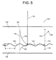
- FIG. 5 shows a silicon CMOS image sensor 100 in accordance with the invention.
- the other details of a silicon CMOS image sensor are known in the art, and are omitted here for the sake of simplicity.
- the silicon CMOS image sensor 100 includes a silicon layer 102 having an incident light surface 104 on one side and a corrugated surface on the opposite side having a periodicity ⁇ and a depth d, and a metal layer 106 having a corrugated surface matching the corrugated surface of the silicon layer 102 (thus having a periodicity ⁇ ) and contacting the corrugated surface of the silicon layer 102 to form a corrugated interface 108 having a periodicity ⁇ between the silicon layer 102 and the metal layer 106.
- the corrugated interface 108 preferably has a nonsinusoidal profile.
- the metal layer 106 may be made out of any metal that is suitable for use in a silicon CMOS image sensor, such as Ag, Au, Al, Ni, or any other suitable metal.
- Ag has the lowest losses for surface plasmons, but is more reactive than Au, so Au might be preferable to use even though it has higher losses for surface plasmons than Ag.
- the metal layer preferably has a thickness in a range from 100 nm to 1000 nm, but any thickness can be used as long as the resulting structure is capable of generating surface plasmons.
- a photon 110 incident on the incident light surface 104 penetrates the silicon layer 102 and is converted to a surface plasmon 112 when it reaches the corrugated interface 108.
- the surface plasmon 112 propagates along the corrugated interface 108 substantially parallel to the light incident surface 104.
- the photon 110 may have any wavelength, but is preferably infrared light. Suitable wavelengths of infrared light are 780 nm and 980 nm, although infrared light having any wavelength may be used.
- the periodicity ⁇ of the corrugated interface 108 is calculated for the wavelength ⁇ 0 of the photon 110 using Equation 10 described above, and may be calculated assuming an incident angle of 0° relative to the normal of the light incident surface 104.
- the depth d of the corrugated interface 108 will affect the efficiency of the coupling between the photon 110 and the surface plasmon 112. If the depth d is too shallow, almost no coupling will occur, since no coupling at all occurs for a flat profile. Also, if the depth d is too deep, for example, on the order of the wavelength of the photon 110, the efficiency of the coupling will be low.
- the optimum depth d may be determined by experimentation since it will depend on the particular configuration being used. However, an optimum depth d for infrared light will probably be between 50 nm and 100 nm.
- the surface plasmon 112 generates an evanescent wave having a component 114 which extends away from the corrugated interface 108 into the silicon layer 102 and a component 116 which extends away from the corrugated interface 108 into the metal layer 106.
- the evanescent wave has an electric field profile which is shown with respect to a reference axis 118 which represents an electric field of zero.
- the component 114 of the evanescent wave which extends into the silicon layer 102 and the component 116 of the evanescent wave which extends into the metal layer 106 decay exponentially as indicated by 120 and 122, respectively, with the component 114 extending into the silicon layer 102 decaying more slowly than the component 116 extending into the metal layer 106.
- the component 114 of the evanescent wave extending into the silicon layer 102 will create an electron-hole pair consisting of a hole 124 and an electron 126. If this occurs, the surface plasmon 112 is absorbed.
- the probability that an electron-hole pair will be created depends on the path length of the surface plasmon 112-the longer the path length, the greater the probability that an electron-hole pair will be created.
- the invention increases the length of the energy absorption path in the silicon layer 102 by converting the photon 110 traveling through the thickness of the silicon layer 102 into the surface plasmon 112 traveling across the width or the length of the silicon layer 102, thus in effect bending the energy absorption path in the silicon layer 102 by 90°.
- the electron 126 created when the surface plasmon 112 is absorbed is collected by the charge collection structure of the silicon CMOS image sensor 100, which is omitted in FIG. 4 for the sake of simplicity.
- FIG. 5 shows that the corrugated interface 108 is formed by a silicon layer 102 and a metal layer 106, and thus is a metal/semiconductor interface.
- a surface plasmon is a phenomenon associated with a metal/dielectric interface.
- a semiconductor has an electrical conductivity intermediate between that of a dielectric (or insulator) and a conductor. Depending on the semiconductor material and any doped impurities in the semiconductor material, any particular semiconductor may be more dielectric-like or more conductor-like.
- a dielectric layer 128 may be provided between the semiconductor layer 102 and the metal layer 106 as shown in FIG. 6, thereby forming a corrugated metal/dielectric interface 130.
- a suitable material for dielectric layer 128 is SiO 2 , but any dielectric material suitable for use in a silicon CMOS image sensor may be used.
- the dielectric layer must be thin enough so that the component 114 of the evanescent wave of the surface plasmon 112 can extend into the silicon layer 102 so it can create an electron-hole pair.
- FIG. 7 shows a modification of the silicon CMOS image sensor 100 in FIG. 5 in which a corrugated interface 132 between the silicon layer 102 and the metal layer 106 has a rectangular profile.
- FIG. 8 shows a modification of the silicon CMOS image sensor 100 in FIG. 6 in which a corrugated interface 134 between the dielectric layer 128 and the metal layer 106 has a rectangular profile.
- the rectangular profiles shown in FIGS. 3, 8, and 9 are not limited to the particular configurations shown in FIGS. 3, 8, and 9, and the period of the rectangular profile, the height and the width of the projections of the rectangular profile, and the ratio of the period of the rectangular profile to the width of the projections of the rectangular profile can be varied as necessary to obtain a suitable rectangular profile.
- the invention is by no means limited to this, and is applicable to any semiconductor sensor receiving radiant energy at any wavelength where surface plasmons can exist.
- Other semiconductors which can be used in the invention besides Si include Ge, AISb, GaSb, GaAs, GaP, InSb, InAs, InP, CdS, CdSe, ZnO, and ZnS, but any semiconductor can be used.
- the invention is by no means limited to this, and is applicable to any device having a semiconductor layer that is too thin to absorb incident radiant energy with a desired energy absorption efficiency, and to any device having a semiconductor layer that absorbs incident radiant energy regardless of whether the semiconductor layer is too thin to absorb the incident radiant energy with a desired energy absorption efficiency.
- the invention is by no means limited to this, and is applicable to a device including a semiconductor layer and a metal layer in which radiant energy is incident on the metal layer, with the metal layer preferably being substantially transparent to the incident radiant energy.
Abstract
Description
- There are many kinds of semiconductor sensors which have many uses. In particular, silicon sensors are widely used in imaging technologies such as video cameras, digital cameras, and optical navigation devices.
- The silicon layer in the silicon CMOS image sensors used in optical navigation devices is typically made as thin as possible to minimize the amount of silicon used and obtain as compact a device as possible. Infrared light tends to pass through the silicon layer in such silicon CMOS image sensors without being absorbed. Thus, the silicon in the silicon CMOS image sensor is too thin to absorb the infrared light with a desired energy absorption efficiency.
- The invention relates to using surface plasmons to increase an energy absorption efficiency of a semiconductor sensor.
- Embodiments in accordance with the invention are described below in conjunction with the accompanying drawings of which:
- FIG. 1 is a graph of energy versus wavenumber showing a relationship between light radiative states or plane wave states lying within a light cone and surface plasmon states lying on surface plasmon dispersion curves, and showing a coupling of a surface plasmon state to a photon state in accordance with the invention;
- FIG. 2 is a diagram of a corrugated surface having a rectangular profile in accordance with the invention;
- FIG. 3 is the Fourier spectrum of the rectangular profile of the corrugated surface shown in FIG. 2 in accordance with the invention;
- FIG. 4 is a graph of energy versus wavenumber showing a relationship between light radiative states or plane wave states lying within a light cone and surface plasmon states lying on surface plasmon dispersion curves, and showing three different couplings of one surface plasmon to three different photons in accordance with the invention;
- FIG. 5 is diagram of a silicon CMOS image sensor showing a photon being converted to a surface plasmon at a corrugated metal/semiconductor interface in accordance with the invention;
- FIG. 6 is diagram of a silicon CMOS image sensor showing a photon being converted to a surface plasmon at a corrugated metal/dielectric interface in accordance with the invention;
- FIG. 7 is a diagram of a silicon CMOS image sensor with a corrugated metal/semiconductor interface having a rectangular profile in accordance with the invention;
- FIG. 8 is a diagram of a silicon CMOS image sensor with a corrugated metal/dielectric interface having a rectangular profile in accordance with the invention.
- Reference will now be made in detail to embodiments in accordance with the invention, examples of which are illustrated in the accompanying drawings, wherein like reference numerals refer to the like elements throughout. The embodiments in accordance with the invention are described below.
- If there were a way to bend the light incident on a silicon CMOS image sensor by 90° after it penetrates into the silicon, the light could then travel across the width of a pixel which might be on the order of 5 to 6 µm wide, rather than through the thickness of the silicon which might be only on the order of 1 µm thick or less, thereby increasing the distance the light travels through the silicon, and thus increasing the probability that the light will be absorbed and create electron-hole pairs This can be done using surface plasmons.
- A surface plasmon can be thought of as a very highly attenuated guided wave that is constrained to follow a metal/dielectric interface, and is a combined oscillation of the electromagnetic field and the surface charges of the metal. A surface plasmon is not a light radiative state or a plane wave because its electric field profile decays exponentially away from the metal/dielectric interface. The electric field of a surface plasmon is called an evanescent wave.
- FIG. 1 shows a graph of energy plotted on a
vertical energy axis 20 versus wavenumber kz plotted on ahorizontal wavenumber axis 22. The wavenumber kz is a component of a wavenumber k parallel to some interface along the Z axis. - The wavenumber k is defined by the following equation:

where λ is a wavelength. - The wavenumber kz is defined by the following equation:

where λ is a wavelength and θ is an angle of incidence measured from the normal to the interface. - The interface is a metal/dielectric interface along which surface plasmons propagate, and the metal/dielectric interface is substantially parallel to a light incident surface of a dielectric layer, which may be a semiconductor layer, such as a silicon layer. Thus, a photon incident on the light incident surface of the dielectric layer travels through the dielectric layer before it reaches the metal/dielectric interface. The wavenumber kZ,PHOTON of such a photon is defined by the following equation:

where λ is the wavelength of the photon in a vacuum, nd is the index of refraction of the dielectric, and θ is the angle of incidence of the photon measured from the normal to the metal/dielectric interface. - Momentum p is defined by the following equation:

where("h bar") is the reduced Planck's constant (Planck's constant divided by 2π), and k is the wavenumber. As can be seen from Equation 4, momentum is directly proportional to wavenumber. Thus, as wavenumber increases along the
wavenumber axis 22 in FIG. 1, momentum also increases. - Energy is inversely proportional to wavelength. Thus, as energy increases along the
energy axis 20 in FIG. 1, wavelength decreases. - Each point in the graph in FIG. 1 represents a photonic state where the properties of that state are its energy (or wavelength) and its wavenumber (or momentum).
- A light radiative state or a plane wave state, that is, light propagating in free space or in some material, always must lie within a
light cone 24 shown in FIG. 1. Thelight cone 24 represents all possible light radiative states or plane wave states. The right half of thelight cone 24 on the right side of theenergy axis 20 represents all possible light radiative states or plane wave states that propagate in a forward direction, and the left half of thelight cone 24 on the left side of theenergy axis 20 represents light radiative states or plane wave states that propagate in a backward direction. Theenergy axis 20 extending through the center of thelight cone 24 represents light radiative states or plane wave states that propagate normal to the interface. Adiagonal line 26 represents light radiative states or plane wave states that propagate parallel to the interface in the forward direction, and adiagonal line 28 represents light radiative states or plane wave states that propagate parallel to the interface in the backward direction. - All possible states of a surface plasmon propagating forward along a metal/dielectric interface are represented by a surface
plasmon dispersion curve 30 to the right of theenergy axis 20, and all possible states of a surface plasmon propagating backward along the metal/dielectric interface are represented by asurface plasmon curve 32 to the left of theenergy axis 20. - In FIG. 1, KZ,SP is a wavenumber of a surface plasmon. The relationship between KZ,SP and a frequency f of the surface plasmon is a dispersion relation for the surface plasmons, and is given by the following equation:

where c is the speed of light, εm is the permittivity of the metal, and εd is the permittivity of the dielectric. However, for any material, ε is a function of frequency, soEquation 5 is more complicated than it appears at first glance. Surface plasmon dispersion curves likesurface plasmon curves Equation 5. Surfaceplasmon dispersion curves light cone 24. - The relationship between frequency f and wavelength λ is given by the following equation:

where c is the speed of light. Substituting this relationship for f inEquation 5 results in the following relationship between the wavenumber kZ,SP of the surface plasmon and a wavelength λ, of the surface plasmon:
- The wavenumber KZ,SP (and thus the momentum) of any state on the surface
plasmon dispersion curve 30 on the right side of theenergy axis 20 in FIG. 1 will always be greater than the wavenumber kZ,PHOTON (and thus the momentum) of any light radiative state at the same energy (or wavelength λ) because the surfaceplasmon dispersion curve 30 lies outside thelight cone 24. The same situation applies on the left side of theenergy axis 20. Thus, any surface plasmon state is a nonradiative state and under normal circumstances can never be coupled with a light radiative state because momentum would not be conserved. - However, this inability to couple a surface plasmon state to a light radiative state can be overcome by introducing a grating or corrugated surface at the metal/dielectric interface. In the presence of a grating or corrugated surface, the wavenumber of any photonic state will change by the following amount:

where A is the periodicity of the grating or corrugated surface, and m is a diffraction order equal to aninteger - Thus, the wavenumber KZ,PHOTON of a photon having a wavelength λ0 as shown in FIG. 1 will increase by 2π/Λ and become equal to the wavenumber kZ,SP of a surface plasmon having the same wavelength λ0. Since the photon and the surface plasmon have the same wavelength, they also have the same energy, and since they now have the same wavenumber, they also now have the same momentum, and therefore the surface plasmon can couple to the photon since both energy and momentum are conserved. This coupling is represented by
line 34 in FIG. 1. Thus, when the photon of wavelength λ0 is incident on the metal/dielectric interface, it is converted into a surface plasmon of wavelength λ0 which propagates along the meta/dielectric interface. The relationship between KZ,SP and KZ,PHOTON in this situation is defined by the following equation:
- Substituting the expressions for kZ,SP and kZ,PHOTON from Equations 4 and 8 above into Equation 9 results in the following equation:

where λ0 is the wavelength λ0 shown in FIG. 1. Equation 10 can be solved to find a periodicity Λ of a grating or corrugated surface required to couple a photon having a wavelength λ0 and an angle of incidence θ measured from a normal to the metal/dielectric interface to a surface plasmon having the same wavelength λ0 propagating along the metal dielectric interface. - As can be seen from Equation 10, any change in either wavelength λ0 or incident angle θ will require a corresponding change in Λ. The periodicity Λ given by Equation 10 is the periodicity of a grating or corrugated surface having a sinusoidal profile. Such a grating or corrugated surface will only couple light of a single wavelength λ0 at a single incident angle θ (or in a very narrow range of incident angles centered about θ) to surface plasmons. However, a silicon CMOS image sensor used in an optical navigation device will typically receive incident light over a range of ±30° from normal.
- To increase the range of incident angles over which light can be coupled to surface plasmons, the grating or corrugated surface may be provided with a non-sinusoidal profile, in effect blurring the sinusoidal profile. Such a non-sinusoidal profile will contain a range of periodicities because any non-sinusoidal profile may be represented as a Fourier series of sinusoidal profiles having different periodicities. A rectangular profile will have a very wide range of periodicities.
- FIG. 2 shows an example of a grating or
corrugated surface 36 having a rectangular profile, wherein Λ is a period of the grating orcorrugated surface 36, w is a width ofprojections 38 of the grating orcorrugated surface 36, and Λ = 10w. - FIG. 3 shows a
Fourier spectrum 40 of the rectangular profile of the grating orcorrugated surface 36 in FIG. 2. The horizontal axis is frequency ω and the vertical axis which extends through ω = 0 is the magnitude F(ω) of theFourier spectrum 40. The vertical bars areFourier components 42 of theFourier spectrum 40, and are equally spaced along the ω) axis by 2π/Λ extending in both directions from ω = 0, that is, at frequencies ω = ±2π/Λ, ±4π/Λ, ±6π/Λ, ±8π/Λ.... A first zero of theFourier spectrum 40 occurs in a vicinity of ω = ±2π/w, or ω = ±20π/Λ since Λ = 10w. - The
Fourier components 42 of the Fourier spectrum in FIG. 3 may be considered to represent sinusoidal profiles having periodicities Λ, Λ/2, Λ/3, Λ/4.... included in the rectangular profile of the grating orcorrugated surface 36 in FIG. 2, and thus represent possible couplings of one surface plasmon to multiple photons having the same wavelength λ and different angles of incidence θ, or having different wavelengths λ and the same angle of incidence θ. - FIG. 4 shows three
different couplings corrugated surface 36 having the rectangular profile shown in FIG. 2 at three different angles of incidence θ represented by thediagonal line 50, theenergy axis 20, and thediagonal line 52. - Coupling 44 is between a surface plasmon having a wavenumber KZ,SP and a photon having a wavenumber KZ,PHOTON 1 which is increased by 2π/Λ, corresponding to the Fourier component having a frequency 2π/Λ shown in FIG. 3 which represents a sinusoidal profile having a periodicity Λ.
-
Coupling 46 is between the surface plasmon having the wavenumber KZ,SP and a photon having a wavenumber KZ,PHOTON 2 = 0 which is increased by 4π/Λ, corresponding to the Fourier component having a frequency 4π/Λ shown in FIG. 3 which represents a sinusoidal profile having a periodicity Λ/2. -
Coupling 48 is between the surface plasmon having a wavenumber kZ,SP and a photon having a wavenumber kZ,PHOTON 3 which is increased by 6π/Λ, corresponding to the Fourier component having a frequency 6π/Λ shown in FIG. 3 which represents a sinusoidal profile having a periodicity Λ/3. - FIG. 5 shows a silicon
CMOS image sensor 100 in accordance with the invention. The other details of a silicon CMOS image sensor are known in the art, and are omitted here for the sake of simplicity. - The silicon
CMOS image sensor 100 includes asilicon layer 102 having an incidentlight surface 104 on one side and a corrugated surface on the opposite side having a periodicity Λ and a depth d, and ametal layer 106 having a corrugated surface matching the corrugated surface of the silicon layer 102 (thus having a periodicity Λ) and contacting the corrugated surface of thesilicon layer 102 to form acorrugated interface 108 having a periodicity Λ between thesilicon layer 102 and themetal layer 106. For the reasons discussed above, thecorrugated interface 108 preferably has a nonsinusoidal profile. - The
metal layer 106 may be made out of any metal that is suitable for use in a silicon CMOS image sensor, such as Ag, Au, Al, Ni, or any other suitable metal. Ag has the lowest losses for surface plasmons, but is more reactive than Au, so Au might be preferable to use even though it has higher losses for surface plasmons than Ag. The metal layer preferably has a thickness in a range from 100 nm to 1000 nm, but any thickness can be used as long as the resulting structure is capable of generating surface plasmons. - A
photon 110 incident on the incidentlight surface 104 penetrates thesilicon layer 102 and is converted to asurface plasmon 112 when it reaches thecorrugated interface 108. Thesurface plasmon 112 propagates along thecorrugated interface 108 substantially parallel to thelight incident surface 104. - The
photon 110 may have any wavelength, but is preferably infrared light. Suitable wavelengths of infrared light are 780 nm and 980 nm, although infrared light having any wavelength may be used. - The periodicity Λ of the
corrugated interface 108 is calculated for the wavelength λ0 of thephoton 110 using Equation 10 described above, and may be calculated assuming an incident angle of 0° relative to the normal of thelight incident surface 104. - The depth d of the
corrugated interface 108 will affect the efficiency of the coupling between thephoton 110 and thesurface plasmon 112. If the depth d is too shallow, almost no coupling will occur, since no coupling at all occurs for a flat profile. Also, if the depth d is too deep, for example, on the order of the wavelength of thephoton 110, the efficiency of the coupling will be low. The optimum depth d may be determined by experimentation since it will depend on the particular configuration being used. However, an optimum depth d for infrared light will probably be between 50 nm and 100 nm. - The
surface plasmon 112 generates an evanescent wave having acomponent 114 which extends away from thecorrugated interface 108 into thesilicon layer 102 and acomponent 116 which extends away from thecorrugated interface 108 into themetal layer 106. The evanescent wave has an electric field profile which is shown with respect to areference axis 118 which represents an electric field of zero. Thecomponent 114 of the evanescent wave which extends into thesilicon layer 102 and thecomponent 116 of the evanescent wave which extends into themetal layer 106 decay exponentially as indicated by 120 and 122, respectively, with thecomponent 114 extending into thesilicon layer 102 decaying more slowly than thecomponent 116 extending into themetal layer 106. - There is a probability that the
component 114 of the evanescent wave extending into thesilicon layer 102 will create an electron-hole pair consisting of ahole 124 and anelectron 126. If this occurs, thesurface plasmon 112 is absorbed. The probability that an electron-hole pair will be created depends on the path length of the surface plasmon 112-the longer the path length, the greater the probability that an electron-hole pair will be created. The invention increases the length of the energy absorption path in thesilicon layer 102 by converting thephoton 110 traveling through the thickness of thesilicon layer 102 into thesurface plasmon 112 traveling across the width or the length of thesilicon layer 102, thus in effect bending the energy absorption path in thesilicon layer 102 by 90°. - The
electron 126 created when thesurface plasmon 112 is absorbed is collected by the charge collection structure of the siliconCMOS image sensor 100, which is omitted in FIG. 4 for the sake of simplicity. - FIG. 5 shows that the
corrugated interface 108 is formed by asilicon layer 102 and ametal layer 106, and thus is a metal/semiconductor interface. However, strictly speaking, a surface plasmon is a phenomenon associated with a metal/dielectric interface. A semiconductor has an electrical conductivity intermediate between that of a dielectric (or insulator) and a conductor. Depending on the semiconductor material and any doped impurities in the semiconductor material, any particular semiconductor may be more dielectric-like or more conductor-like. - While it is believed that most semiconductors will be sufficiently dielectric-like to enable generation of surface plasmons at a metal/semiconductor interface, there may some semiconductors for which this is not the case. Accordingly, to ensure that surface plasmons will always be generated, a
dielectric layer 128 may be provided between thesemiconductor layer 102 and themetal layer 106 as shown in FIG. 6, thereby forming a corrugated metal/dielectric interface 130. A suitable material fordielectric layer 128 is SiO2, but any dielectric material suitable for use in a silicon CMOS image sensor may be used. The dielectric layer must be thin enough so that thecomponent 114 of the evanescent wave of thesurface plasmon 112 can extend into thesilicon layer 102 so it can create an electron-hole pair. - FIG. 7 shows a modification of the silicon
CMOS image sensor 100 in FIG. 5 in which acorrugated interface 132 between thesilicon layer 102 and themetal layer 106 has a rectangular profile. - FIG. 8 shows a modification of the silicon
CMOS image sensor 100 in FIG. 6 in which acorrugated interface 134 between thedielectric layer 128 and themetal layer 106 has a rectangular profile. - The rectangular profiles shown in FIGS. 3, 8, and 9 are not limited to the particular configurations shown in FIGS. 3, 8, and 9, and the period of the rectangular profile, the height and the width of the projections of the rectangular profile, and the ratio of the period of the rectangular profile to the width of the projections of the rectangular profile can be varied as necessary to obtain a suitable rectangular profile.
- While the embodiments in accordance with the invention have been described above as being applicable to a silicon CMOS image sensor receiving infrared light, the invention is by no means limited to this, and is applicable to any semiconductor sensor receiving radiant energy at any wavelength where surface plasmons can exist. Other semiconductors which can be used in the invention besides Si include Ge, AISb, GaSb, GaAs, GaP, InSb, InAs, InP, CdS, CdSe, ZnO, and ZnS, but any semiconductor can be used.
- While the embodiments in accordance with the invention have been described above as being applicable to a silicon CMOS image sensor in which the silicon layer is too thin to absorb incident infrared light with a desired energy absorption efficiency, the invention is by no means limited to this, and is applicable to any device having a semiconductor layer that is too thin to absorb incident radiant energy with a desired energy absorption efficiency, and to any device having a semiconductor layer that absorbs incident radiant energy regardless of whether the semiconductor layer is too thin to absorb the incident radiant energy with a desired energy absorption efficiency.
- While the embodiments in accordance with the invention have been described above as being applicable to a device including a semiconductor layer and a metal layer in which radiant energy is incident on the semiconductor layer, the invention is by no means limited to this, and is applicable to a device including a semiconductor layer and a metal layer in which radiant energy is incident on the metal layer, with the metal layer preferably being substantially transparent to the incident radiant energy.
- Although a few embodiments in accordance with the invention have been shown and described, it would be appreciated by those skilled in the art that changes may be made in these embodiments without departing from the principles and spirit of the invention, the scope of which is defined in the claims and their equivalents.
Claims (7)
- A semiconductor sensor (100) comprising:a semiconductor layer (102) having an incident surface (104) to receive incident radiant energy (110) on one side of the semiconductor layer (102) and having a corrugated surface on an opposite side of the semiconductor layer (102); anda metal layer (106) having a corrugated surface matching the corrugated surface of the semiconductor layer (102) and contacting the corrugated surface of the semiconductor layer (102) to form a corrugated interface (108) between the semiconductor layer (102) and the metal layer (106), the corrugated interface (108) being substantially parallel to the incident surface (104) of the semiconductor layer (102);wherein the corrugated interface (108) between the semiconductor layer (102) and the metal layer (104) provides an energy absorption path over which the incident radiant energy (110) is absorbed.
- The semiconductor sensor (100) of claim 1, wherein the incident radiant energy (110) comprises photons that penetrate the semiconductor layer (102) and are incident on the corrugated interface (108) where the photons are converted into surface plasmons (112) that travel along the corrugated interface (108) substantially parallel to the incident surface (104) of the semiconductor layer (102) and generate evanescent waves (116) that extend into the semiconductor layer (102) and generate electron-hole pairs (124, 126) in the semiconductor layer (102).
- The semiconductor sensor (100) of claim 2, wherein the surface plasmons (112) are absorbed when the evanescent waves (116) generate the electron-hole pairs (124, 126) in the semiconductor layer (102).
- The semiconductor sensor (100) of claim 1, wherein the corrugated interface (108) has a nonsinusoidal profile (108, 132).
- The semiconductor sensor (100) of claim 1, wherein the corrugated interface (108) has a substantially rectangular profile (132).
- The semiconductor sensor (100) of claim 1, wherein the incident radiant energy (110) penetrates the semiconductor layer (102) and is incident on the corrugated interface (108); and
wherein the corrugated interface (108) has a periodicity A defined by the following equation:
where λ0 is a wavelength of the incident radiant energy (110), εm is a permittivity of the metal layer (106), εd is a permittivity of the semiconductor layer (102), nd is an index of refraction of the semiconductor layer (102), and θ is an angle of incidence of the incident radiant energy (110) measured from a normal to the corrugated interface (108). - The semiconductor sensor (100) of claim 1, wherein the semiconductor sensor (100) is a silicon CMOS image sensor (100); and
wherein the incident radiant energy (110) is infrared light (110).
Applications Claiming Priority (1)
| Application Number | Priority Date | Filing Date | Title |
|---|---|---|---|
| US11/331,267 US7538405B2 (en) | 2006-01-13 | 2006-01-13 | Semiconductor sensor using surface plasmons to increase energy absorption efficiency |
Publications (2)
| Publication Number | Publication Date |
|---|---|
| EP1808901A2 true EP1808901A2 (en) | 2007-07-18 |
| EP1808901A3 EP1808901A3 (en) | 2008-07-23 |
Family
ID=38005361
Family Applications (1)
| Application Number | Title | Priority Date | Filing Date |
|---|---|---|---|
| EP06013963A Withdrawn EP1808901A3 (en) | 2006-01-13 | 2006-07-05 | Semiconductor sensor using surface plasmons to increase energy absorption efficiency |
Country Status (3)
| Country | Link |
|---|---|
| US (1) | US7538405B2 (en) |
| EP (1) | EP1808901A3 (en) |
| CN (1) | CN100573893C (en) |
Families Citing this family (5)
| Publication number | Priority date | Publication date | Assignee | Title |
|---|---|---|---|---|
| US7623165B2 (en) * | 2006-02-28 | 2009-11-24 | Aptina Imaging Corporation | Vertical tri-color sensor |
| FR2910632B1 (en) * | 2006-12-22 | 2010-08-27 | Commissariat Energie Atomique | OPTICAL PLASMON ENCODING DEVICE AND AUTHENTICATION METHOD EMPLOYING THE SAME |
| US7943908B2 (en) * | 2007-01-22 | 2011-05-17 | University Of Maryland | Sensor system with surface-plasmon-polariton (SPP) enhanced selective fluorescence excitation and method |
| WO2009070665A1 (en) * | 2007-11-27 | 2009-06-04 | Massachusetts Institute Of Technology | Near field detector for integrated surface plasmon resonance biosensor applications |
| US10535701B2 (en) | 2016-01-12 | 2020-01-14 | Omnivision Technologies, Inc. | Plasmonic-nanostructure sensor pixel |
Citations (4)
| Publication number | Priority date | Publication date | Assignee | Title |
|---|---|---|---|---|
| US4482779A (en) * | 1983-04-19 | 1984-11-13 | The United States Of America As Represented By The Administrator Of National Aeronautics And Space Administration | Inelastic tunnel diodes |
| US5157537A (en) * | 1991-02-01 | 1992-10-20 | Yeda Research And Development Co., Ltd. | Distributed resonant cavity light beam modulator |
| US5841143A (en) * | 1997-07-11 | 1998-11-24 | The United States Of America As Represented By Administrator Of The National Aeronautics And Space Administration | Integrated fluorescene |
| US20050269578A1 (en) * | 2002-08-02 | 2005-12-08 | Barnes William L | Optoelectronic devices |
Family Cites Families (8)
| Publication number | Priority date | Publication date | Assignee | Title |
|---|---|---|---|---|
| US4178604A (en) * | 1973-10-05 | 1979-12-11 | Hitachi, Ltd. | Semiconductor laser device |
| US4583818A (en) * | 1983-08-08 | 1986-04-22 | Gte Laboratories Incorporated | Optical device with surface plasmons |
| JPS62198169A (en) * | 1986-02-25 | 1987-09-01 | Fuji Electric Corp Res & Dev Ltd | Solar cell |
| US5404373A (en) * | 1991-11-08 | 1995-04-04 | University Of New Mexico | Electro-optical device |
| JPH10117006A (en) * | 1996-08-23 | 1998-05-06 | Kanegafuchi Chem Ind Co Ltd | Thin-film photoelectric conversion device |
| US5991488A (en) * | 1996-11-08 | 1999-11-23 | The Arizona Board Of Regents On Behalf Of The University Of Arizona | Coupled plasmon-waveguide resonance spectroscopic device and method for measuring film properties |
| US7248297B2 (en) * | 2001-11-30 | 2007-07-24 | The Board Of Trustees Of The Leland Stanford Junior University | Integrated color pixel (ICP) |
| JP4034153B2 (en) * | 2002-09-20 | 2008-01-16 | ユーディナデバイス株式会社 | Semiconductor photo detector |
-
2006
- 2006-01-13 US US11/331,267 patent/US7538405B2/en not_active Expired - Fee Related
- 2006-07-05 EP EP06013963A patent/EP1808901A3/en not_active Withdrawn
-
2007
- 2007-01-12 CN CNB2007100008431A patent/CN100573893C/en not_active Expired - Fee Related
Patent Citations (4)
| Publication number | Priority date | Publication date | Assignee | Title |
|---|---|---|---|---|
| US4482779A (en) * | 1983-04-19 | 1984-11-13 | The United States Of America As Represented By The Administrator Of National Aeronautics And Space Administration | Inelastic tunnel diodes |
| US5157537A (en) * | 1991-02-01 | 1992-10-20 | Yeda Research And Development Co., Ltd. | Distributed resonant cavity light beam modulator |
| US5841143A (en) * | 1997-07-11 | 1998-11-24 | The United States Of America As Represented By Administrator Of The National Aeronautics And Space Administration | Integrated fluorescene |
| US20050269578A1 (en) * | 2002-08-02 | 2005-12-08 | Barnes William L | Optoelectronic devices |
Non-Patent Citations (1)
| Title |
|---|
| DMITRUK N L: "Physical properties of surface-barrier structure with microrelief semiconductor-metal interface" MICROELECTRONICS, 1995. PROCEEDINGS., 1995 20TH INTERNATIONAL CONFEREN CE ON NIS, SERBIA 12-14 SEPT. 1995, NEW YORK, NY, USA,IEEE, US, vol. 1, 12 September 1995 (1995-09-12), pages 425-429, XP010161722 ISBN: 978-0-7803-2786-3 * |
Also Published As
| Publication number | Publication date |
|---|---|
| US20070164377A1 (en) | 2007-07-19 |
| CN100573893C (en) | 2009-12-23 |
| CN101000917A (en) | 2007-07-18 |
| US7538405B2 (en) | 2009-05-26 |
| EP1808901A3 (en) | 2008-07-23 |
Similar Documents
| Publication | Publication Date | Title |
|---|---|---|
| US7623165B2 (en) | Vertical tri-color sensor | |
| Collin et al. | Efficient light absorption in metal–semiconductor–metal nanostructures | |
| US8208191B2 (en) | Ultra-wide band slow light structure using plasmonic graded grating structures | |
| Zhang | Resonant terahertz transmission in plasmonic arrays of subwavelength holes | |
| US8653431B2 (en) | Photoelectric conversion device and image sensor | |
| EP1808901A2 (en) | Semiconductor sensor using surface plasmons to increase energy absorption efficiency | |
| Cansizoglu et al. | A new paradigm in high-speed and high-efficiency silicon photodiodes for communication—Part I: Enhancing photon–material interactions via low-dimensional structures | |
| Ndiaye et al. | Giant optical field enhancement in multi-dielectric stacks by photon scanning tunneling microscopy | |
| Reininger et al. | Photonic crystal slab quantum cascade detector | |
| Steglich et al. | Improvement of Ge-on-Si photodiodes by black silicon light trapping | |
| El Abouti et al. | Optical Tamm states in one-dimensional superconducting photonic crystal | |
| Zhu et al. | Guided mode resonance enabled ultra-compact germanium photodetector for 1.55 μm detection | |
| US7622703B2 (en) | Photodetector having a near field concentration | |
| Fu et al. | Optical coupling in quantum well infrared photodetector by diffraction grating | |
| Kaushik et al. | Efficient sub-bandgap photodetection via two-dimensional electron gas in ZnO based heterojunction | |
| Liu et al. | Enhanced light trapping in Ge-on-Si-on-insulator photodetector by guided mode resonance effect | |
| US20110202323A1 (en) | Photodetectors using resonance and method of making | |
| Chen et al. | Time-resolved photocurrents in quantum well/dot infrared photodetectors with different optical coupling structures | |
| Wang et al. | 40 GHz waveguide-integrated two-dimensional palladium diselenide photodetectors | |
| Lee et al. | Leaky-mode effects in plasmonic-coupled quantum dot infrared photodetectors | |
| Berini | Surface plasmon photodetectors | |
| Fischer et al. | Plasmonics-integrated Ge PIN-photodetectors: efficiency enhancement by Al nanoantennas and plasmon detection | |
| Maleki et al. | Photocurrent enhancement of graphene photodetectors by photon tunneling of light into surface plasmons | |
| Yalcin et al. | Spectral bandwidth and phase effects of resonantly excited ultrafast surface plasmon pulses | |
| Song et al. | Graphene based waveguides |
Legal Events
| Date | Code | Title | Description |
|---|---|---|---|
| PUAI | Public reference made under article 153(3) epc to a published international application that has entered the european phase |
Free format text: ORIGINAL CODE: 0009012 |
|
| AK | Designated contracting states |
Kind code of ref document: A2 Designated state(s): AT BE BG CH CY CZ DE DK EE ES FI FR GB GR HU IE IS IT LI LT LU LV MC NL PL PT RO SE SI SK TR |
|
| AX | Request for extension of the european patent |
Extension state: AL BA HR MK YU |
|
| RAP1 | Party data changed (applicant data changed or rights of an application transferred) |
Owner name: AVAGO TECHNOLOGIES GENERAL IP (SINGAPORE) PTE. LTD |
|
| PUAL | Search report despatched |
Free format text: ORIGINAL CODE: 0009013 |
|
| AK | Designated contracting states |
Kind code of ref document: A3 Designated state(s): AT BE BG CH CY CZ DE DK EE ES FI FR GB GR HU IE IS IT LI LT LU LV MC NL PL PT RO SE SI SK TR |
|
| AX | Request for extension of the european patent |
Extension state: AL BA HR MK RS |
|
| RIC1 | Information provided on ipc code assigned before grant |
Ipc: H01L 31/0236 20060101ALI20080619BHEP Ipc: H01L 31/09 20060101ALI20080619BHEP Ipc: H01L 31/0352 20060101AFI20070515BHEP |
|
| 17P | Request for examination filed |
Effective date: 20080811 |
|
| AKX | Designation fees paid |
Designated state(s): DE |
|
| 17Q | First examination report despatched |
Effective date: 20090814 |
|
| STAA | Information on the status of an ep patent application or granted ep patent |
Free format text: STATUS: THE APPLICATION IS DEEMED TO BE WITHDRAWN |
|
| 18D | Application deemed to be withdrawn |
Effective date: 20120201 |