EP1755125A1 - Method for operating a programmable metallization cell and electrical circuit - Google Patents
Method for operating a programmable metallization cell and electrical circuit Download PDFInfo
- Publication number
- EP1755125A1 EP1755125A1 EP05017790A EP05017790A EP1755125A1 EP 1755125 A1 EP1755125 A1 EP 1755125A1 EP 05017790 A EP05017790 A EP 05017790A EP 05017790 A EP05017790 A EP 05017790A EP 1755125 A1 EP1755125 A1 EP 1755125A1
- Authority
- EP
- European Patent Office
- Prior art keywords
- voltage
- pmc
- cell
- line
- memory
- Prior art date
- Legal status (The legal status is an assumption and is not a legal conclusion. Google has not performed a legal analysis and makes no representation as to the accuracy of the status listed.)
- Granted
Links
- 238000001465 metallisation Methods 0.000 title claims abstract description 23
- 238000000034 method Methods 0.000 title claims abstract description 22
- 230000015654 memory Effects 0.000 claims abstract description 93
- 230000008859 change Effects 0.000 claims abstract description 17
- 239000007784 solid electrolyte Substances 0.000 claims abstract description 11
- 230000005684 electric field Effects 0.000 claims abstract description 8
- 239000003792 electrolyte Substances 0.000 description 18
- 239000000463 material Substances 0.000 description 11
- 238000010586 diagram Methods 0.000 description 6
- 230000005669 field effect Effects 0.000 description 6
- 229910052751 metal Inorganic materials 0.000 description 5
- 239000002184 metal Substances 0.000 description 5
- 230000002441 reversible effect Effects 0.000 description 4
- 230000000630 rising effect Effects 0.000 description 4
- 239000004020 conductor Substances 0.000 description 3
- 239000002001 electrolyte material Substances 0.000 description 3
- 101150090474 ERS2 gene Proteins 0.000 description 2
- PXHVJJICTQNCMI-UHFFFAOYSA-N Nickel Chemical compound [Ni] PXHVJJICTQNCMI-UHFFFAOYSA-N 0.000 description 2
- 230000008901 benefit Effects 0.000 description 2
- 150000004770 chalcogenides Chemical class 0.000 description 2
- 230000006870 function Effects 0.000 description 2
- 239000010416 ion conductor Substances 0.000 description 2
- 150000002500 ions Chemical class 0.000 description 2
- 229910021645 metal ion Inorganic materials 0.000 description 2
- 238000004377 microelectronic Methods 0.000 description 2
- 239000004065 semiconductor Substances 0.000 description 2
- 229910052709 silver Inorganic materials 0.000 description 2
- 239000004332 silver Substances 0.000 description 2
- RYGMFSIKBFXOCR-UHFFFAOYSA-N Copper Chemical compound [Cu] RYGMFSIKBFXOCR-UHFFFAOYSA-N 0.000 description 1
- 101150031726 ERS1 gene Proteins 0.000 description 1
- ZOKXTWBITQBERF-UHFFFAOYSA-N Molybdenum Chemical compound [Mo] ZOKXTWBITQBERF-UHFFFAOYSA-N 0.000 description 1
- 108010076504 Protein Sorting Signals Proteins 0.000 description 1
- 101100204733 Schizosaccharomyces pombe (strain 972 / ATCC 24843) gus1 gene Proteins 0.000 description 1
- 239000003990 capacitor Substances 0.000 description 1
- 238000006243 chemical reaction Methods 0.000 description 1
- 230000000295 complement effect Effects 0.000 description 1
- 229910052802 copper Inorganic materials 0.000 description 1
- 239000010949 copper Substances 0.000 description 1
- 230000008878 coupling Effects 0.000 description 1
- 238000010168 coupling process Methods 0.000 description 1
- 238000005859 coupling reaction Methods 0.000 description 1
- 230000006378 damage Effects 0.000 description 1
- 230000007423 decrease Effects 0.000 description 1
- 230000001419 dependent effect Effects 0.000 description 1
- 230000003467 diminishing effect Effects 0.000 description 1
- 239000011521 glass Substances 0.000 description 1
- 229910044991 metal oxide Inorganic materials 0.000 description 1
- 150000004706 metal oxides Chemical class 0.000 description 1
- 150000002739 metals Chemical class 0.000 description 1
- 229910052750 molybdenum Inorganic materials 0.000 description 1
- 239000011733 molybdenum Substances 0.000 description 1
- 229910052759 nickel Inorganic materials 0.000 description 1
- BASFCYQUMIYNBI-UHFFFAOYSA-N platinum Chemical compound [Pt] BASFCYQUMIYNBI-UHFFFAOYSA-N 0.000 description 1
- 229910021420 polycrystalline silicon Inorganic materials 0.000 description 1
- 229920000642 polymer Polymers 0.000 description 1
- 229920005591 polysilicon Polymers 0.000 description 1
- 230000008569 process Effects 0.000 description 1
- 238000006479 redox reaction Methods 0.000 description 1
- 229910021332 silicide Inorganic materials 0.000 description 1
- 239000006104 solid solution Substances 0.000 description 1
- 230000036962 time dependent Effects 0.000 description 1
- WFKWXMTUELFFGS-UHFFFAOYSA-N tungsten Chemical compound [W] WFKWXMTUELFFGS-UHFFFAOYSA-N 0.000 description 1
- 229910052721 tungsten Inorganic materials 0.000 description 1
- 239000010937 tungsten Substances 0.000 description 1
Images


Classifications
-
- G—PHYSICS
- G11—INFORMATION STORAGE
- G11C—STATIC STORES
- G11C13/00—Digital stores characterised by the use of storage elements not covered by groups G11C11/00, G11C23/00, or G11C25/00
- G11C13/0002—Digital stores characterised by the use of storage elements not covered by groups G11C11/00, G11C23/00, or G11C25/00 using resistive RAM [RRAM] elements
- G11C13/0009—RRAM elements whose operation depends upon chemical change
- G11C13/0011—RRAM elements whose operation depends upon chemical change comprising conductive bridging RAM [CBRAM] or programming metallization cells [PMCs]
Definitions
- the present invention refers to a method for operating a programmable metallization cell of a conductive-bridging random access memory, particularly for use in a CBRAM memory circuit.
- the present invention further relates to a memory circuit comprising a programmable metallization cell.
- PMC programmable metallization cell
- CBRAM conductive-bridging random access memory
- the storing of different states in a PMC memory cell is based on the developing or diminishing of a conductive path in the electrolyte material between electrodes based on an applied electrical field. Although the electrolyte material has a high resistance, the conductive path between electrodes has a low resistance. Thereby, the PMC memory cell can be set to different states depending on the resistance of the PMC memory element. Usually, both states of the PMC memory cell are sufficiently time-stable in such a way that data may permanently be stored.
- a PMC memory cell is operated by applying a positive or a negative voltage to the solid electrolyte of the PMC memory element.
- the PMC memory cell In order to store data into the PMC memory cell, the PMC memory cell is brought to a programmed stated by applying a suitable programming voltage to the PMC memory cell which results in the development of the conductive path in the electrolyte material and therefore in the setting of a first state with low resistance.
- an erase voltage has to be supplied in such a manner that the resistance of the PMC memory cell changes back to a high resistance which refers to an erased state.
- a read voltage To read out a PMC memory cell, a read voltage is applied that is lower than the programming voltage. With the read voltage, a current through the resistance of the PMC memory element is detected and associated to the respective low or high resistance state of the PMC memory cell.
- US 6,865,117 B2 describes a programming circuit for a programmable microelectronic device, a system including the circuit and a method for forming the same.
- the circuit is configured to provide a reversible bias across the microelectronic device to perform erase and write functions.
- One configuration of the programming circuit includes one or more inputs and a complementary metal-oxide semiconductor circuit coupled to the programmable device. This design allows for writing and erasing of the programmable cell using a low and a high voltage input.
- a high voltage is applied to the anode and a low voltage is applied to the cathode or, respectively, a low voltage is applied to the anode and a high voltage is applied to the cathode of the PMC cell.
- the object of the present invention is to provide a method for operating a programmable metallization cell of a conductive-bridging random access memory by which the programming operation is enhanced. Furthermore, another aspect of the present invention is to provide a method for operating the programmable metallization cell that uses a lower programming voltage.
- a further aspect of the invention is to provide an electrical circuit comprising a programmable metallization cell with a solid electrolyte that can be programmed with lower voltages during a writing or an erasing operation.
- the present invention is a method for operating a programmable metallization cell of a conductive bridging random access memory (CBRAM).
- the CBRAM memory comprises plate lines, bit lines and memory cells.
- Each memory cell comprises a programmable metallization cell (PMC) and a switch, whereby a memory cell is arranged between a bit line and a plate line.
- Resistance values of the memory cells are programmable by applying different voltages to the PMC cells by changing the voltage value on the bit line, whereby the voltage on the plate line is changed with respect to the voltage of the bit line for increasing a voltage drop over the PMC cell to assist the programming of the PMC cell.
- the present invention is an electrical circuit, comprising first lines, a plate line, and memory cells with PMC cells.
- Each memory cell comprises a programmable metallization cell with a solid electrolyte which is adapted to selectively develop or diminish a conductive path depending on the applied electrical field.
- a memory cell is arranged between a first and a plate line.
- Many PMC memory cells are connected with the same plate line.
- a writing unit is disposed configured to change a state of a PMC cell to a programmed state by applying a program voltage on the first line to the memory cell and to change the state of the PMC cell to an erased state by applying an erase voltage to the memory cell.
- a voltage unit connected with the plate line and configured to apply a first voltage to the second plate line according to a writing process and to apply a second voltage to the plate line according to an erasing operation of the PMC cell that is connected with the plate line to increase the voltage drop over the PMC memory cell to assist the writing and the erasing operation.
- the present invention relates to a CBRAM memory circuit, comprising a plate line, bit lines, word lines and memory cells.
- the memory cells comprise programmable metallization cells (PMC cell) with a solid electrolyte which is adapted to selectively develop or diminish a conductive path depending on the applied electrical field and a switch.
- a memory cell is arranged between a bit line and the plate line, whereby a controlling input of the switch is connected to the word line.
- a word line driver circuit configured to select one of the word lines and to change a voltage of the selected word line to close or open the switch.
- a writing unit configured to change a state of a respective PMC cell to a programmed state by applying a program voltage to the respective PMC cell and to change the state of the respective PMC cell to an erased state by applying an erase voltage.
- a voltage unit connected with the plate line and configured to apply a plate voltage to the plate line according to a programming or an erasing operation of the PMC cell to increase the voltage drop over the PMC cell to assist the programming or the erasing operation.
- the present invention is based on the idea of providing a method for operating a programmable metallization cell which uses available voltage levels of a circuit or device more efficiently.
- This object is achieved by connecting the memory cells to a plate line and by changing the voltage on the plate line during an erasing or a programming operation.
- the voltage on the plate line is changed to a different direction compared to the voltage on the bit line. This has the advantage that two electrical potentials with small difference could be used for programming the PMC cell.
- the idea of changing the voltage on the plate line could be used in any electrical circuit that comprises a PMC cell with a solid electrolyte which is adapted to selectively develop or diminish a conductive path depending on the applied electrical field.
- this idea can be advantageously used in a CBRAM memory circuit providing a simple design that uses two electric potentials of the CBRAM memory circuit which are available on the CBRAM memory and have a small difference for programming and erasing the PMC cell.
- the present invention may be described in terms of various functional components. It should be appreciated that such functional components may be realized by any number of hardware or structural components configured to perform the specified functions. For example, the present invention may employ various integrated components comprised of various electrical devices, e.g. resistors, transistors, capacitors, diodes and such like, the values of which may be suitably configured for various intended purposes. In addition, the present invention may be practiced in any integrated circuit application where an effective reversible polarity is desired. Such general applications which may be appreciated by those skilled in the art in light of the present disclosure are not described in detail. Further, it should be noted that while various components may be suitably coupled or connected to other components within exemplary circuits, such connections and couplings can be realized by direct connection between components and by connection through other components and devices located in between.
- the present invention generally relates to a method for operating a programmable metallization cell of a conductive bridging random access memory, an electrical circuit comprising a PMC cell with a solid electrolyte and a CBRAM memory cell comprising programmable metallization cells.
- Figure 1 depicts a conductive bridging junction of a PMC cell 1 comprising an anode 2, a cathode 4 and an electrolyte layer 3 in between.
- the cathode 4 is connected to a ground potential and the anode 2 may be connected to a high potential in the depicted situation that shows a programming operation.
- the structure shown in Figure 1 may be used in order to store information and thus may be used in memory circuits.
- the conductive bridging junction or other programmable structure in accordance with the present invention may be suitably used in memory devices to replace DRAM, SRAM, PROM, EEPROM, flash devices or any combination of such memories.
- programmable structures of the present invention may be used for other applications where programming or changing of electrical properties of a portion of an electrical circuit are desired.
- the electrolyte layer 3 is formed by material which conducts ions upon application of a sufficient voltage. Suitable materials for ion conductors include polymers, glasses and semiconductor materials. In one exemplary embodiment of the invention, the electrolyte layer 3 is formed by chalcogenides material. The electrolyte layer 3 may also suitably include dissolved and/or dispersed conductive material. For example, the electrolyte layer 3 may comprise a solid solution that includes dissolved metals and/or metal ions. The chalcogenides materials including silver, copper, combinations of these materials and such like could be used for constituting the electrolyte layer 3.
- the anode 2 and the cathode 4 may be formed by any suitable conductive material.
- the anode 2 and the cathode 4 may be formed by doped polysilicon material or metal.
- one of the electrodes, i.e. the anode 2 is formed by a material including a metal which dissolves in ion conductors when a sufficient bias is applied across the electrodes and the other electrode, i.e. the cathode is relatively inert and does not dissolve during operating of the programmable device.
- the first electrode 2 may be an anode during a write operation and be comprised of a material including silver which dissolves in the electrolyte layer.
- the second electrode 4 may be a cathode during the write operation and be comprised of an inert material such as tungsten, nickel, molybdenum, platinum, metal silicides, and such like.
- the conductive bridging junction is configured in such a way that when a bias larger than a threshold voltage is applied across the electrodes 2, 4, the electrical properties of the electrolyte layer 3 change. If a voltage is applied larger than the threshold voltage, conductive ions within the electrolyte layer start to migrate and to form a region having an increased conductivity compared to the conductor at or near the more negative of the electrodes 2, 4. As the conductive region forms, the resistance between the electrodes 2, 4 decreases and other electrical properties may also change. If the same voltage is applied in reverse, the conductive region will dissolve back into the electrolyte layer and the device will return to a high resistance or erased state.
- the basic reaction is if a higher voltage is applied at the anode 2, a redox reaction at the cathode 4 drives metal ions from the reactive anode into the electrolyte layer 3. Therefore, in the electrolyte layer 3, metal-rich clusters are formed. The result is a conductive bridge that occurs between the anode and the cathode. If a reverse voltage is applied to the PMC cell 1, the metal-rich clusters are dissolved and the conductive bridge is degraded.
- FIG. 2 shows a diagram of the voltage and the current occurring during a programming operation, a read operation and an erase operation of a PMC cell 1.
- the PMC cell is not programmed and therefore has a high resistance. If a voltage is applied with a higher voltage at the anode 2 and a lower voltage at the cathode 4, no current flows through the PMC cell 1 until a threshold voltage V1 is applied. With the voltage rising over the threshold voltage V1, current starts to flow until a working current IW is achieved which is confined by the programming circuit. The voltage is then reduced to 0 Volt, whereby the current falls to 0 A. Now the PMC cell is programmed.
- a sensing voltage is applied to the PMC cell which is lower than the threshold voltage V1.
- the sensing voltage VS may be about 0.1 Volt. Due to the sensing voltage, a working current IW flows through the PMC cell. Without the programming operation, no current would flow through the PMC cell applied to a sensing voltage.
- a lower voltage i.e. a negative voltage is applied to the anode 2 starting at 0 Volt. Up to a negative voltage of about -0.1 Volt, a negative current flows through the PMC cell 1, but when the negative voltage drops over - 0.1 Volt, the current goes down to 0 A. Now the PMC cell 1 again has the same high resistance as prior to the programming operation.
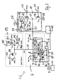
- Figure 3 depicts parts of an electrical circuit 46 i.e. a CBRAM comprising memory cells 5, 6, 47 with PMC cells 1, 12, 42 that are connected to a common plate line 11.
- the plate line 11 constitutes a conductive line or area that is connected with many PMC cells 1, 12, 42.
- the memory cells 5, 6, 47 are connected to first lines 8, 44 with a writing unit 15, 45 and with second lines 9, 10 with a controlling unit 41.
- the plate line 11 is connected to a voltage unit 29.
- a sensing unit 40 is connected to the first and further first line 8, 44.
- two memory cells 5, 6 are arranged which comprise a first and a second PMC cell 1, 12, the anodes of which are connected to a first and second switch 13, 14.
- the first and the second switch 13, 14 are connected to the first line 8.
- controlling inputs of the first and the second switch 13, 14 are connected to a second line 9 and to a further second line 10, respectively.
- the writing unit 15 comprises a first input 16 and a second input 17.
- the first input 16 is a programming input and the second input 17 is an erasing input.
- the writing unit 15 comprises a voltage source with different potentials 26, 28. Depending on the signals on the first input 16 and the second input 17, a high or a low voltage 28, 26 is applied to the first line 8.
- the writing unit 15 preferably comprises a current source 21.
- the current source 21 confines the maximum current which flows from the writing unit 15 to the first line 8 during a programming operation.
- the sensing unit 40 is connected to the first line 8 and is configured to detect a current on the first line 8.
- a voltage unit 29 is disposed that comprises in a first embodiment a third input 31 and a fourth input 32.
- the third input 31 is disposed for controlling an erasing operation and the fourth input 32 is disposed for controlling a programming operation.
- the voltage unit 29 comprises a voltage source 35, 36 with different potentials.
- the voltage unit 29 applies different voltages to the plate line 11 depending on the input signals on the third input 31 and the fourth input 32. For example, if a programming operation is performed, the controlling unit 41 selects one of the second or further second lines 9, 10 and applies a high voltage to a selected second line 9. According to the high voltage on the second line 9, the first switch 13 is closed providing a conductive connection between the anode 2 of the first PMC cell 1 and the first line 8.
- a programming signal is put on the first input 16 of the writing unit 15.
- the writing unit 15 applies a high voltage of about 3.4 Volt on the first line 8.
- the further program signal is put on the fourth input 32 of the voltage unit 29.
- the voltage unit 29 applies a low voltage to the plate line 11.
- the low voltage is about 0 Volt, i.e. ground potential, but certainly lower than the high voltage that is applied by the writing unit 15 on the first line 8. This results in a bias voltage over the PMC cell 1 which has a voltage difference between the low voltage of the voltage unit 29 on the plate line 11 and the high voltage of the writing unit 15 on the first line 8.
- the resistance of the first PMC cell is changed from a high resistance to a low resistance as explained in accordance with Figure 2.
- the controlling unit 41 changes the voltage on the second line 9 to a low voltage opening the first switch 13.
- the further program signal is stopped at the first input 16 and therefore, the writing unit 15 stops to apply a high voltage to the second line 8.
- the program signal is stopped on the fourth input 32 and therefore, the voltage unit 29 stops to apply the low voltage to the plate line 11.
- an erasing operation is carried out.
- the controlling unit 41 selects the second line 9 and applies a high voltage on the second line 9.
- the high voltage on the second line 9 closes the first switch 13 connecting the anode 2 of the first PMC cell 1 with the second line 8.
- an erasing signal is put on the second input 17.
- the writing unit 15 applies a low voltage to the second line 8.
- a further erasing signal is put on the third input 31 causing the voltage unit 29 to apply a high voltage to the plate line 11.
- the erasing signal is stopped on the second input 17.
- the write unit 15 stops applying a low voltage to the second line 8.
- the further erasing signal is stopped on the third input 31 of the voltage unit 29. Consequently, the voltage unit 29 stops to apply a high voltage to the plate line 11.
- the controlling unit 41 stops to apply a high voltage on the first word line 9. This results in opening the first switch 13 disconnecting the first PMC cell 1 from the first line 8.
- the voltage unit 29 comprises a fifth input 37 for a read signal. Furthermore, the voltage unit 29 comprises a read voltage source 38. If the state of the first PMC cell 1 is to be sensed, the controlling unit 41 applies a voltage to the second line 9, closing the first switch 13. Furthermore, a read signal is put on the fifth input 37 of the voltage unit 29. This causes the voltage unit 29 to connect the plate line 11 to the read voltage source 38. The read voltage source 38 applies a read voltage on the plate line 11. Furthermore, the sensing unit 40 is connected to the first line 8 applying a respective potential on the first bit line 8 to generate a read voltage drop in the electrolyte layer 3. The read voltage drop is about 0.1 Volt.
- the sensing unit 40 detects no current over the PMC cell 1 if the first PMC cell 1 is in a high resistance state. If the first PMC cell 1 is in a low resistive state, the sensing unit 40 detects a working current IW over the first PMC cell 1. Therefore, the sensing unit 40 is able to check whether the first PMC cell 1 is in a low or in a high resistive state.
- the first PMC cell 1 can be used to store a data, e.g. the data "0" for a low resistive state and the data "1" for a high resistive state which can be checked by the sensing unit 40.
- the writing unit 15 comprises a high potential contact 26 and a low potential contact 28.
- the low potential contact 28 may be connected to ground potential and the high potential contact 26 may be connected to an internal high potential of the electrical circuit 47.
- the high potential contact 26 is additionally connected to a current mirror 20 with the current source 21 which induces the current of the current source 21 on a second branch that connects the high potential contact 26 with a third switch 18.
- a controlling contact of the third switch 18 is connected with the first input 16.
- An output of the third switch 18 is connected to a connecting point 27.
- the low potential contact 28 is connected to an input of a fourth switch 19, the output of which is connected to the connecting point 27.
- a controlling contact of the fourth switch 19 is connected to the second input 17.
- the connecting point 27 is connected with the first line 8.
- the fourth switch 19 is constituted as an n-channel field effect transistor and the third switch 18 is constituted as a p-channel field effect transistor 18. If a low voltage is applied to the controlling contact of the third switch 18, the third switch 18 is switched into a current state. Furthermore, if a high voltage is applied to the second input 17, the fourth switch 19 is closed, connecting the connecting point 27 to the low potential contact 28.
- the current mirror 20 comprises a first transistor 22 in series with the current source 21 which is connected to a ground potential. An input of the first transistor 22 is connected to the high potential contact 27. Furthermore, a second transistor 23 is arranged in between the high potential contact 26 and the third switch 18.
- the first and the second transistor 22, 23 are realized as p-channel field effect transistors.
- the gates of the first and the second transistor 22, 23 are connected by a connecting line 24.
- the connecting line 24 is connected by a second connecting line 25 with an input of the current source 21 that is connected to the first transistor 22.
- the current source 21 confines the maximum current flowing through the closed third switch 18 during a program operation. This helps to avoid a destruction of the PMC cells 1, 12.
- the voltage unit 29 comprises a second high potential contact 35 that is connected with a high voltage source and a second low potential contact 36 which is connected with a low voltage source, e.g. with ground potential.
- a third transistor 33 and a fourth transistor 34 are arranged in series.
- a second connecting point 30 is arranged connected to the plate line 11.
- the third transistor 33 is realized as a p-channel field effect transistor and the fourth transistor 34 is realized as an n-channel field effect transistor.
- a gate contact of the third transistor 33 is connected to the third input 31.
- a gate contact of the fourth transistor 34 is connected to the fourth input 32.
- a fifth transistor 39 realized as an n-channel field effect transistor is disposed between the read voltage source 38 and the plate line 11. A gate contact of the fifth transistor 39 is connected to the fifth input 37.
- the program operation, the reading operation and the erasing operation that was explained above regarding the first PMC cell 1 is the same with the second PMC cell 12 whereby instead of the second line 9 the further second line 10 has to be activated by the controlling unit 41 closing the second switch 14.
- the other operation steps are the same.
- the first line 8 constitutes a first bit line and the second line 9 constitutes a first word line and the further second line 10 constitutes a second word line.
- a large array 7 with a lot of PMC cells is disposed whereby the PMC cells of the array are connected by the cathodes to a common plate line 11.
- a lot of bit lines and a lot of word lines are arranged in a crossed net structure, whereby at the crossing points of a bit and a word line memory cell 5, 6 are arranged. If there are a lot of bit lines 8, for each bit line a writing unit 15 may be provided or a common writing unit 15 is used which is connected to selected bit lines by a multiplexer unit.
- Figure 4 shows a plate voltage VPL of the plate line 11, in a second time line, a word voltage WL of a second line, in a third time line, a program signal PRG on a first input 16, in a fourth time line, an erase signal ERS on the second input 17, in a fifth time line, a read signal READ on the fifth input 37, and in a sixth time line a voltage drop VCELL of the first PMC cell 1 over the time axis.
- a first programming cycle used to write e.g. the data "1" into a non-programmed first PMC cell 1 starts shortly before a first point of time t 1 by rising the word voltage WL on first line 9.
- the plate voltage VPL of the plate line 11 is changed from a medium value to a low value by applying a high voltage on the fourth input 32 closing the fourth transistor 34.
- the fourth transistor 34 connects the plate line 11 which has a medium level of voltage with ground potential.
- the medium value of the voltage of the plate line 11 may be half of an internal voltage VINT of the electrical circuit.
- the low voltage of the plate line 11 is reached shortly after a second point of time t 2 .
- the program signal PRG is put on the first input 16 and the voltage on the gate of the third switch 18 is lowered to 0 Volt.
- This turns the third switch 18 into a current state applying a high voltage on the first line 8.
- the first switch 13 is in a current state, as well, according to the high voltage on the second line 9.
- the low voltage of 0 Volt is applied and the anode 2 of the first PMC cell 1 is connected to the high voltage of the high potential contact 26.
- a voltage drop VCELL over the first PMC cell 1 rises between a third and a fourth point of time t 3 , t 4 , over the threshold voltage V1.
- the voltage drop approximately has the value of the internal voltage VINT of the high potential contact 26.
- a voltage drop VCELL over the threshold changes the resistance in the electrolyte layer 3.
- the program signal PRG on the first input 16 is raised from the low voltage to the high voltage opening the third switch 18.
- the plate voltage on the plate line 11 is subsequently raised to a medium level.
- the voltage drop VCELL over the PMC cell 1 drops to 0 Volt.
- the word voltage WL on the second line 9 is reduced to 0 Volt.
- the programming of the PMC cell 1 is erased that means that the data 0 is stored in the PMC cell 1.
- the second cycle is started raising the word voltage WL on the second line 9 shortly before a seventh point of time t 7 .
- the potential of the plate line 11 is raised from the medium value to a high value.
- an erasing signal ERS is put on the second input 17.
- the erasing signal increases the voltage on the gate contact of the fourth switch 19.
- the fourth switch 19 is switched into a current state connecting the low potential contact 28 to the first line 8.
- the erasing signal ERS on the second input 17 is lowered to 0 Volt. This causes a fall of the voltage drop VCELL across the PMC cell 1. Furthermore, the potential of the plate line 11 is reduced after a tenth point of time t 10 from the high state to a medium value. Finally, the word voltage WL of the second line 9 is lowered to a low voltage. The time during which the voltage drop VCELL is applied to the electrolyte layer 3 of the PMC cell 1 lasts as long as it is necessary to dissolve the conductive connection between the two electrodes of the PMC cell 1. After the second cycle, the PMC cell 1 has the same high resistance as prior to the first cycle 1.
- the potential of the plate line 11 is changed in a contrary direction compared to the potential of the first line 8. Therefore, available potential sources, e.g. a ground voltage and a high voltage of a device, may preferably be used for achieving a high voltage drop during an erasing and a programming operation of the PMC cell and additionally provide a medium voltage on the plate line 11 during other periods of time.
- available potential sources e.g. a ground voltage and a high voltage of a device
- the programming state of the PMC cell 1 is sensed.
- the sensing operation starts with a rising potential on the second line 9 shortly before a thirteenth point of time t 13 up to a high level.
- a read signal READ is applied to the fifth input 37 connecting the read voltage source 38 to the plate line 11.
- the voltage of the read voltage source 38 is lower than the threshold voltage V1 necessary to program the PMC cell 1.
- the sensing unit 40 detects a voltage drop VREAD determined by the third voltage source 38 and a current depending on the program state of the PMC cell. In our embodiment, the PMC cell 1 has been erased before the reading operation, therefore unit 40 senses no current during the read status.
- the read signal READ is put to 0 Volt and the potential on the second line 9 is put to 0 Volt, as well. This causes the voltage drop VCELL to fall from a high level VREAD to a 0 level.
- Figure 5 shows a time-dependent diagram of the plate potential VPL of the plate line 11, the word potential of a second line 9, a read signal READ which is applied to the fifth input 37 of the voltage unit 29, a first programming signal PRG1n that is applied to a first input 16 of the writing unit 15, a first erasing signal ERS1 which is applied to a second input 17 of the writing unit 15, a voltage drop VCELL1 across the first PMC cell 1, a second programming signal PRG2n of a second writing unit 15, which is applied to a corresponding input of the further writing unit 45, a second erasing signal ERS2 which is put on a corresponding second input of the second writing unit 45 and a second voltage drop VCELL2 across the third PMC cell 42.
- Figure 5 depicts a further method for writing, erasing and reading data for different PMC cells 1, 42.
- two PMC cells 1, 42 are connected with respective switches 13, 43 comprising one common second line 9, e.g. a word line.
- the bit lines 8, 44 of the first and third PMC cells 1, 42 are connected to a common writing unit or respective writing units 15, 45.
- the third PMC cell 42 is connected by a fifth switch 43 to the further first line 44 that is connected with a further writing unit 45.
- the structure of the further writing unit 45 is identical to the writing unit 15.
- the word voltage WL of the common second line 9 is raised from a low level to a high level at a first point of time t 1 .
- the plate potential VPL of the plate line 11 is raised from a medium value to a high value starting shortly before a second point of time t 2 .
- the high level is maintained until a fourth point of time t 4 is reached.
- the plate potential VPL of the plate line 11 is changed from the high value to a low level which is e.g. the mass potential and is lower than the medium value.
- the low level is kept on the plate line 11 until a sixth point of time t 6 .
- the potential of the plate line 11 is raised to the medium value.
- the word voltage WL of the second line 9 is maintained at the high value shortly before a seventh point of time t 7 and then lowered to the low level.
- the high voltage on the second line 9 results in closed switches 13, 43 which connect the first PMC cell 1 and the third PMC cell 42 to respective first and third lines 9, 44 representing bit lines.
- the program signal on the first input 16 is lowered from a high value to a low value.
- a further erasing signal ERS2 of the further writing unit 45 is raised from a low value to a high value.
- the high value on the erasing input of the further writing unit connects the third line 44 of the further first PMC cell 42 to a low voltage.
- the plate line 11 that is connected to a cathode of the third PMC cell 42 is on a high level. This results in a voltage drop VCELL2 on the third PMC cell 42 which is higher than the threshold erasing voltage.
- the third PMC cell 45 is applied to an erasing voltage between the third point of time t 3 and the fourth point of time t 4 .
- the resistive state of the third PMC cell 45 is erased between the third and the fourth point of time t 3 , t 4 .
- a date "0" is programmed in the third PMC cell. Due to the change of the potential of the plate line 11 around the fourth point of time t 4 , the voltage drop VCELL2 along the third PMC cell 45 falls to 0 Volt shortly after the fourth point of time t 4 . Shortly before the fourth point of time t 4 , a voltage drop VCELL1 along the first PMC cell 1 rises from 0 Volt up to a high level. The high level voltage is maintained until shortly before the fifth point of time t 5 and falls back to the 0 voltage. Between the fourth and the fifth point of time t 4 , t 5 , the resistive state of the first PMC cell 1 is changed to a low resistance and therefore the first PMC cell is programmed to date "1".
- the advantage of this programming method is that memory cells may be programmed with different data at the same time.
- the first PMC cell 1 is programmed with a low resistance corresponding to data "1” and the third PMC cell 42 is programmed with a high resistance corresponding to data "0". This is shown in cycle 1 of Figure 5.
- a low resistance is programmed in the first PMC cell 1 and a low resistance is programmed in the third PMC cell 42.
- the plate potential VPL of the plate line 11 is firstly raised from the medium level up to a high level during a first time period and secondly lowered to a ground level during a second time period and finally raised to the medium level. This is the same procedure as in the first cycle 1.
- the word potential WL of the second line 9 is also raised during the whole cycle from a basic level to a high level and subsequently returned to the basic level.
- the first program signal PRG1n is lowered from the high level to the low level during the first time period in which the plate potential VPL is at a high level and at a low level during the second time period in which the plate line is on a low level.
- the plate potential is high and the voltage on the first line 8 is high.
- no programming of the first PMC cell 1 occurs.
- this results in a high first voltage drop VCELL1 across the first PMC cell.
- the first PMC cell is programmed to low resistance.
- the second program signal PRG2n is lowered from a high level during the second cycle 2 in the same time as the first program signal PRG1n to a low level and then raised to a high level again.
- the lowering of the second program signal PRG2n results in connecting the further bit line with high potential. This occurs during the second time period which is between an eleventh point of time t 11 and a twelfth point of time t 12 in a positive and high second voltage drop VCELL2 which results in a programming of the third PMC cell 42 with a low resistance.
- the PMC cells 1, 42 connected to a common second line e.g. a common word line and a common plate line 11, may be programmed with different resistance values and thus with different data during one cycle.
- a reading operation is shown for two PMC cells 1, 42 which are connected to the same plate line 11 and are connected to the same second line 9. Furthermore, the two PMC cells 1, 42 are connected with two different first lines 8, 44 and the two different first lines are each connected to the sensing unit 40.
- the plate voltage VPL on the plate line is kept constant, the voltage on the second line 9 is raised to close the respective switches 13, 43 of the two memory cells 5, 47 to connect the respective PMC cells 1, 42 to respective first lines 8, 44.
- the read signal READ is applied to the fifth input 37 of the voltage unit 29.
- the fifth transistor 39 is closed connecting the plate line 11 to the read voltage source 38 applying a read voltage to the cathodes of the PMC cells 1, 42 which are connected to the plate line 11.
- the first lines 8, 44 of the two memory cells are held at a potential which results in a voltage drop on the two PMC cells 1, 42, the voltage drop being in a range lower than the threshold voltage. This is shown in Figure 5 with the first voltage drop VCELL1 and the second voltage drop VCELL2.
- the sensing signals that are measured by the sensing unit 40 are not shown in the diagram. Previously, the two PMC cells 1, 42 were programmed in the second cycle to a low resistance level. Thus, on the two first lines 8, 44 of the two memory cells 5, 47 the sensing unit 40 detects a small current corresponding to the low resistive state of the PMC cells.
Abstract
Description
- The present invention refers to a method for operating a programmable metallization cell of a conductive-bridging random access memory, particularly for use in a CBRAM memory circuit. The present invention further relates to a memory circuit comprising a programmable metallization cell.
- Memory cells comprising a solid electrolyte material are well known as PMC (programmable metallization cell) memory cells. Memory devices including such PMC memory cells are known as CBRAM (conductive-bridging random access memory) devices. The storing of different states in a PMC memory cell is based on the developing or diminishing of a conductive path in the electrolyte material between electrodes based on an applied electrical field. Although the electrolyte material has a high resistance, the conductive path between electrodes has a low resistance. Thereby, the PMC memory cell can be set to different states depending on the resistance of the PMC memory element. Usually, both states of the PMC memory cell are sufficiently time-stable in such a way that data may permanently be stored.
- A PMC memory cell is operated by applying a positive or a negative voltage to the solid electrolyte of the PMC memory element. In order to store data into the PMC memory cell, the PMC memory cell is brought to a programmed stated by applying a suitable programming voltage to the PMC memory cell which results in the development of the conductive path in the electrolyte material and therefore in the setting of a first state with low resistance. In order to store a second state in the PMC memory cell with high resistance, an erase voltage has to be supplied in such a manner that the resistance of the PMC memory cell changes back to a high resistance which refers to an erased state. To read out a PMC memory cell, a read voltage is applied that is lower than the programming voltage. With the read voltage, a current through the resistance of the PMC memory element is detected and associated to the respective low or high resistance state of the PMC memory cell.
-
US 6,865,117 B2 describes a programming circuit for a programmable microelectronic device, a system including the circuit and a method for forming the same. The circuit is configured to provide a reversible bias across the microelectronic device to perform erase and write functions. One configuration of the programming circuit includes one or more inputs and a complementary metal-oxide semiconductor circuit coupled to the programmable device. This design allows for writing and erasing of the programmable cell using a low and a high voltage input. Depending on the state that should be programmed into the PMC cell, a high voltage is applied to the anode and a low voltage is applied to the cathode or, respectively, a low voltage is applied to the anode and a high voltage is applied to the cathode of the PMC cell. - The object of the present invention is to provide a method for operating a programmable metallization cell of a conductive-bridging random access memory by which the programming operation is enhanced. Furthermore, another aspect of the present invention is to provide a method for operating the programmable metallization cell that uses a lower programming voltage.
- A further aspect of the invention is to provide an electrical circuit comprising a programmable metallization cell with a solid electrolyte that can be programmed with lower voltages during a writing or an erasing operation.
- This objects are achieved by a method for operating a programmable metallization cell according to
claim 1 and an electrical circuit according to claim 8. Furthermore, the objects are achieved by a memory circuit according to claim 9 and a CBRAM memory circuit according toclaim 10. - Preferred embodiments of the present invention are defined in the dependent claims.
- The present invention is a method for operating a programmable metallization cell of a conductive bridging random access memory (CBRAM). The CBRAM memory comprises plate lines, bit lines and memory cells. Each memory cell comprises a programmable metallization cell (PMC) and a switch, whereby a memory cell is arranged between a bit line and a plate line. Resistance values of the memory cells are programmable by applying different voltages to the PMC cells by changing the voltage value on the bit line, whereby the voltage on the plate line is changed with respect to the voltage of the bit line for increasing a voltage drop over the PMC cell to assist the programming of the PMC cell.
- Furthermore, the present invention is an electrical circuit, comprising first lines, a plate line, and memory cells with PMC cells. Each memory cell comprises a programmable metallization cell with a solid electrolyte which is adapted to selectively develop or diminish a conductive path depending on the applied electrical field. A memory cell is arranged between a first and a plate line. Many PMC memory cells are connected with the same plate line. Furthermore, a writing unit is disposed configured to change a state of a PMC cell to a programmed state by applying a program voltage on the first line to the memory cell and to change the state of the PMC cell to an erased state by applying an erase voltage to the memory cell. Furthermore, a voltage unit connected with the plate line and configured to apply a first voltage to the second plate line according to a writing process and to apply a second voltage to the plate line according to an erasing operation of the PMC cell that is connected with the plate line to increase the voltage drop over the PMC memory cell to assist the writing and the erasing operation.
- Furthermore, the present invention relates to a CBRAM memory circuit, comprising a plate line, bit lines, word lines and memory cells. The memory cells comprise programmable metallization cells (PMC cell) with a solid electrolyte which is adapted to selectively develop or diminish a conductive path depending on the applied electrical field and a switch. A memory cell is arranged between a bit line and the plate line, whereby a controlling input of the switch is connected to the word line. Furthermore, a word line driver circuit configured to select one of the word lines and to change a voltage of the selected word line to close or open the switch. Furthermore, a writing unit configured to change a state of a respective PMC cell to a programmed state by applying a program voltage to the respective PMC cell and to change the state of the respective PMC cell to an erased state by applying an erase voltage. Subsequently, a voltage unit connected with the plate line and configured to apply a plate voltage to the plate line according to a programming or an erasing operation of the PMC cell to increase the voltage drop over the PMC cell to assist the programming or the erasing operation.
- The present invention is based on the idea of providing a method for operating a programmable metallization cell which uses available voltage levels of a circuit or device more efficiently. This object is achieved by connecting the memory cells to a plate line and by changing the voltage on the plate line during an erasing or a programming operation. The voltage on the plate line is changed to a different direction compared to the voltage on the bit line. This has the advantage that two electrical potentials with small difference could be used for programming the PMC cell.
- The idea of changing the voltage on the plate line could be used in any electrical circuit that comprises a PMC cell with a solid electrolyte which is adapted to selectively develop or diminish a conductive path depending on the applied electrical field. Particularly, this idea can be advantageously used in a CBRAM memory circuit providing a simple design that uses two electric potentials of the CBRAM memory circuit which are available on the CBRAM memory and have a small difference for programming and erasing the PMC cell.
- These and other objects and features of the present invention will become clear from the following description taken in conjunction with the accompanying drawings in which:
- Figure 1 is a schematic view of a conductive-bridging junction of a PMC cell;
- Figure 2 shows a diagram of the current depending on the voltage drop over the PMC cell for a program, read and erase state;
- Figure 3 depicts a part of a CBRAM memory;
- Figure 4 shows a diagram for a writing, an erasing and a reading operation; and
- Figure 5 depicts a diagram for a signal sequence for a writing, an erasing and a reading operation of two PMC cells during one cycle.
- The present invention may be described in terms of various functional components. It should be appreciated that such functional components may be realized by any number of hardware or structural components configured to perform the specified functions. For example, the present invention may employ various integrated components comprised of various electrical devices, e.g. resistors, transistors, capacitors, diodes and such like, the values of which may be suitably configured for various intended purposes. In addition, the present invention may be practiced in any integrated circuit application where an effective reversible polarity is desired. Such general applications which may be appreciated by those skilled in the art in light of the present disclosure are not described in detail. Further, it should be noted that while various components may be suitably coupled or connected to other components within exemplary circuits, such connections and couplings can be realized by direct connection between components and by connection through other components and devices located in between.
- The present invention generally relates to a method for operating a programmable metallization cell of a conductive bridging random access memory, an electrical circuit comprising a PMC cell with a solid electrolyte and a CBRAM memory cell comprising programmable metallization cells.
- In a schematic view, Figure 1 depicts a conductive bridging junction of a
PMC cell 1 comprising ananode 2, acathode 4 and anelectrolyte layer 3 in between. Thecathode 4 is connected to a ground potential and theanode 2 may be connected to a high potential in the depicted situation that shows a programming operation. - The structure shown in Figure 1 may be used in order to store information and thus may be used in memory circuits. For example, the conductive bridging junction or other programmable structure in accordance with the present invention may be suitably used in memory devices to replace DRAM, SRAM, PROM, EEPROM, flash devices or any combination of such memories. In addition, programmable structures of the present invention may be used for other applications where programming or changing of electrical properties of a portion of an electrical circuit are desired.
- The
electrolyte layer 3 is formed by material which conducts ions upon application of a sufficient voltage. Suitable materials for ion conductors include polymers, glasses and semiconductor materials. In one exemplary embodiment of the invention, theelectrolyte layer 3 is formed by chalcogenides material. Theelectrolyte layer 3 may also suitably include dissolved and/or dispersed conductive material. For example, theelectrolyte layer 3 may comprise a solid solution that includes dissolved metals and/or metal ions. The chalcogenides materials including silver, copper, combinations of these materials and such like could be used for constituting theelectrolyte layer 3. - The
anode 2 and thecathode 4 may be formed by any suitable conductive material. For example, theanode 2 and thecathode 4 may be formed by doped polysilicon material or metal. In accordance with one exemplary embodiment of the present invention, one of the electrodes, i.e. theanode 2, is formed by a material including a metal which dissolves in ion conductors when a sufficient bias is applied across the electrodes and the other electrode, i.e. the cathode is relatively inert and does not dissolve during operating of the programmable device. Thefirst electrode 2 may be an anode during a write operation and be comprised of a material including silver which dissolves in the electrolyte layer. Thesecond electrode 4 may be a cathode during the write operation and be comprised of an inert material such as tungsten, nickel, molybdenum, platinum, metal silicides, and such like. - The conductive bridging junction is configured in such a way that when a bias larger than a threshold voltage is applied across the
electrodes electrolyte layer 3 change. If a voltage is applied larger than the threshold voltage, conductive ions within the electrolyte layer start to migrate and to form a region having an increased conductivity compared to the conductor at or near the more negative of theelectrodes electrodes - The basic reaction is if a higher voltage is applied at the
anode 2, a redox reaction at thecathode 4 drives metal ions from the reactive anode into theelectrolyte layer 3. Therefore, in theelectrolyte layer 3, metal-rich clusters are formed. The result is a conductive bridge that occurs between the anode and the cathode. If a reverse voltage is applied to thePMC cell 1, the metal-rich clusters are dissolved and the conductive bridge is degraded. - Figure 2 shows a diagram of the voltage and the current occurring during a programming operation, a read operation and an erase operation of a
PMC cell 1. At the start, the PMC cell is not programmed and therefore has a high resistance. If a voltage is applied with a higher voltage at theanode 2 and a lower voltage at thecathode 4, no current flows through thePMC cell 1 until a threshold voltage V1 is applied. With the voltage rising over the threshold voltage V1, current starts to flow until a working current IW is achieved which is confined by the programming circuit. The voltage is then reduced to 0 Volt, whereby the current falls to 0 A. Now the PMC cell is programmed. - If the program status is to be sensed or read, a sensing voltage is applied to the PMC cell which is lower than the threshold voltage V1. The sensing voltage VS may be about 0.1 Volt. Due to the sensing voltage, a working current IW flows through the PMC cell. Without the programming operation, no current would flow through the PMC cell applied to a sensing voltage. To erase the program status, a lower voltage, i.e. a negative voltage is applied to the
anode 2 starting at 0 Volt. Up to a negative voltage of about -0.1 Volt, a negative current flows through thePMC cell 1, but when the negative voltage drops over - 0.1 Volt, the current goes down to 0 A. Now thePMC cell 1 again has the same high resistance as prior to the programming operation. - Figure 3 depicts parts of an electrical circuit 46 i.e. a CBRAM comprising
memory cells PMC cells common plate line 11. Theplate line 11 constitutes a conductive line or area that is connected withmany PMC cells memory cells first lines 8, 44 with awriting unit 15, 45 and withsecond lines 9, 10 with a controllingunit 41. Theplate line 11 is connected to avoltage unit 29. Furthermore, asensing unit 40 is connected to the first and furtherfirst line 8, 44. - In a simple embodiment, two
memory cells 5, 6 are arranged which comprise a first and asecond PMC cell second switch second switch second switch second line 10, respectively. - The
writing unit 15 comprises afirst input 16 and asecond input 17. Thefirst input 16 is a programming input and thesecond input 17 is an erasing input. Furthermore, thewriting unit 15 comprises a voltage source withdifferent potentials first input 16 and thesecond input 17, a high or alow voltage writing unit 15 preferably comprises a current source 21. The current source 21 confines the maximum current which flows from thewriting unit 15 to the first line 8 during a programming operation. Thesensing unit 40 is connected to the first line 8 and is configured to detect a current on the first line 8. - A
voltage unit 29 is disposed that comprises in a first embodiment athird input 31 and afourth input 32. Thethird input 31 is disposed for controlling an erasing operation and thefourth input 32 is disposed for controlling a programming operation. Furthermore, thevoltage unit 29 comprises avoltage source 35, 36 with different potentials. Thevoltage unit 29 applies different voltages to theplate line 11 depending on the input signals on thethird input 31 and thefourth input 32. For example, if a programming operation is performed, the controllingunit 41 selects one of the second or furthersecond lines 9, 10 and applies a high voltage to a selected second line 9. According to the high voltage on the second line 9, thefirst switch 13 is closed providing a conductive connection between theanode 2 of thefirst PMC cell 1 and the first line 8. Additionally, a programming signal is put on thefirst input 16 of thewriting unit 15. According to the programming signal, thewriting unit 15 applies a high voltage of about 3.4 Volt on the first line 8. Furthermore, the further program signal is put on thefourth input 32 of thevoltage unit 29. According to this program signal, thevoltage unit 29 applies a low voltage to theplate line 11. For example, the low voltage is about 0 Volt, i.e. ground potential, but certainly lower than the high voltage that is applied by thewriting unit 15 on the first line 8. This results in a bias voltage over thePMC cell 1 which has a voltage difference between the low voltage of thevoltage unit 29 on theplate line 11 and the high voltage of thewriting unit 15 on the first line 8. - During the programming operation, the resistance of the first PMC cell is changed from a high resistance to a low resistance as explained in accordance with Figure 2. After the programming, the controlling
unit 41 changes the voltage on the second line 9 to a low voltage opening thefirst switch 13. Furthermore, the further program signal is stopped at thefirst input 16 and therefore, thewriting unit 15 stops to apply a high voltage to the second line 8. Additionally, the program signal is stopped on thefourth input 32 and therefore, thevoltage unit 29 stops to apply the low voltage to theplate line 11. - If the state of the
first PMC cell 1 is to be changed from low resistance to high resistance, an erasing operation is carried out. For erasing the state of thefirst PMC cell 1, the controllingunit 41 selects the second line 9 and applies a high voltage on the second line 9. The high voltage on the second line 9 closes thefirst switch 13 connecting theanode 2 of thefirst PMC cell 1 with the second line 8. Additionally, an erasing signal is put on thesecond input 17. According to the erasing signal on thesecond input 17, thewriting unit 15 applies a low voltage to the second line 8. Accordingly, a further erasing signal is put on thethird input 31 causing thevoltage unit 29 to apply a high voltage to theplate line 11. Therefore, a negative voltage is applied to theelectrolyte layer 3 higher than the erasing voltage. As a result, the conductive bridging is dissolved and thePMC cell 1 acquires a high resistance again. To end the erasing operation, the erasing signal is stopped on thesecond input 17. Thus, thewrite unit 15 stops applying a low voltage to the second line 8. Furthermore, the further erasing signal is stopped on thethird input 31 of thevoltage unit 29. Consequently, thevoltage unit 29 stops to apply a high voltage to theplate line 11. Furthermore, the controllingunit 41 stops to apply a high voltage on the first word line 9. This results in opening thefirst switch 13 disconnecting thefirst PMC cell 1 from the first line 8. - In a further embodiment, the
voltage unit 29 comprises afifth input 37 for a read signal. Furthermore, thevoltage unit 29 comprises a read voltage source 38. If the state of thefirst PMC cell 1 is to be sensed, the controllingunit 41 applies a voltage to the second line 9, closing thefirst switch 13. Furthermore, a read signal is put on thefifth input 37 of thevoltage unit 29. This causes thevoltage unit 29 to connect theplate line 11 to the read voltage source 38. The read voltage source 38 applies a read voltage on theplate line 11. Furthermore, thesensing unit 40 is connected to the first line 8 applying a respective potential on the first bit line 8 to generate a read voltage drop in theelectrolyte layer 3. The read voltage drop is about 0.1 Volt. Depending on the state of thePMC cell 1, thesensing unit 40 detects no current over thePMC cell 1 if thefirst PMC cell 1 is in a high resistance state. If thefirst PMC cell 1 is in a low resistive state, thesensing unit 40 detects a working current IW over thefirst PMC cell 1. Therefore, thesensing unit 40 is able to check whether thefirst PMC cell 1 is in a low or in a high resistive state. Thus, thefirst PMC cell 1 can be used to store a data, e.g. the data "0" for a low resistive state and the data "1" for a high resistive state which can be checked by thesensing unit 40. - In a simple embodiment, the
writing unit 15 comprises a highpotential contact 26 and a lowpotential contact 28. The lowpotential contact 28 may be connected to ground potential and the highpotential contact 26 may be connected to an internal high potential of theelectrical circuit 47. The highpotential contact 26 is additionally connected to acurrent mirror 20 with the current source 21 which induces the current of the current source 21 on a second branch that connects the highpotential contact 26 with athird switch 18. A controlling contact of thethird switch 18 is connected with thefirst input 16. An output of thethird switch 18 is connected to a connectingpoint 27. - The low
potential contact 28 is connected to an input of afourth switch 19, the output of which is connected to the connectingpoint 27. A controlling contact of thefourth switch 19 is connected to thesecond input 17. The connectingpoint 27 is connected with the first line 8. - Preferably, the
fourth switch 19 is constituted as an n-channel field effect transistor and thethird switch 18 is constituted as a p-channelfield effect transistor 18. If a low voltage is applied to the controlling contact of thethird switch 18, thethird switch 18 is switched into a current state. Furthermore, if a high voltage is applied to thesecond input 17, thefourth switch 19 is closed, connecting the connectingpoint 27 to the lowpotential contact 28. - The
current mirror 20 comprises afirst transistor 22 in series with the current source 21 which is connected to a ground potential. An input of thefirst transistor 22 is connected to the highpotential contact 27. Furthermore, asecond transistor 23 is arranged in between the highpotential contact 26 and thethird switch 18. The first and thesecond transistor second transistor line 24. The connectingline 24 is connected by a second connectingline 25 with an input of the current source 21 that is connected to thefirst transistor 22. The current source 21 confines the maximum current flowing through the closedthird switch 18 during a program operation. This helps to avoid a destruction of thePMC cells - In a further embodiment, the
voltage unit 29 comprises a second highpotential contact 35 that is connected with a high voltage source and a second low potential contact 36 which is connected with a low voltage source, e.g. with ground potential. Between the second highpotential contact 25 and the second low potential contact 36, athird transistor 33 and afourth transistor 34 are arranged in series. Between the third and thefourth transistor point 30 is arranged connected to theplate line 11. Thethird transistor 33 is realized as a p-channel field effect transistor and thefourth transistor 34 is realized as an n-channel field effect transistor. A gate contact of thethird transistor 33 is connected to thethird input 31. A gate contact of thefourth transistor 34 is connected to thefourth input 32. - Furthermore, a
fifth transistor 39 realized as an n-channel field effect transistor is disposed between the read voltage source 38 and theplate line 11. A gate contact of thefifth transistor 39 is connected to thefifth input 37. - The program operation, the reading operation and the erasing operation that was explained above regarding the
first PMC cell 1 is the same with thesecond PMC cell 12 whereby instead of the second line 9 the furthersecond line 10 has to be activated by the controllingunit 41 closing thesecond switch 14. The other operation steps are the same. - Depending on the electronic device in which the PMC cells are disposed, e.g. in case of a CBRAM memory device, the first line 8 constitutes a first bit line and the second line 9 constitutes a first word line and the further
second line 10 constitutes a second word line. Furthermore, in a memory alarge array 7 with a lot of PMC cells is disposed whereby the PMC cells of the array are connected by the cathodes to acommon plate line 11. In the case of a CBRAM, a lot of bit lines and a lot of word lines are arranged in a crossed net structure, whereby at the crossing points of a bit and a wordline memory cell 5, 6 are arranged. If there are a lot of bit lines 8, for each bit line awriting unit 15 may be provided or acommon writing unit 15 is used which is connected to selected bit lines by a multiplexer unit. - In a first time line, Figure 4 shows a plate voltage VPL of the
plate line 11, in a second time line, a word voltage WL of a second line, in a third time line, a program signal PRG on afirst input 16, in a fourth time line, an erase signal ERS on thesecond input 17, in a fifth time line, a read signal READ on thefifth input 37, and in a sixth time line a voltage drop VCELL of thefirst PMC cell 1 over the time axis. - A first programming cycle used to write e.g. the data "1" into a non-programmed
first PMC cell 1 starts shortly before a first point of time t1 by rising the word voltage WL on first line 9. In a following step, the plate voltage VPL of theplate line 11 is changed from a medium value to a low value by applying a high voltage on thefourth input 32 closing thefourth transistor 34. Thefourth transistor 34 connects theplate line 11 which has a medium level of voltage with ground potential. The medium value of the voltage of theplate line 11 may be half of an internal voltage VINT of the electrical circuit. The low voltage of theplate line 11 is reached shortly after a second point of time t2. When the plate voltage reaches the low level, the program signal PRG is put on thefirst input 16 and the voltage on the gate of thethird switch 18 is lowered to 0 Volt. This turns thethird switch 18 into a current state applying a high voltage on the first line 8. Furthermore, thefirst switch 13 is in a current state, as well, according to the high voltage on the second line 9. On the cathode of thefirst PMC cell 1, the low voltage of 0 Volt is applied and theanode 2 of thefirst PMC cell 1 is connected to the high voltage of the highpotential contact 26. Thus, a voltage drop VCELL over thefirst PMC cell 1 rises between a third and a fourth point of time t3, t4, over the threshold voltage V1. The voltage drop approximately has the value of the internal voltage VINT of the highpotential contact 26. As explained above, a voltage drop VCELL over the threshold changes the resistance in theelectrolyte layer 3. After a predetermined time, the program signal PRG on thefirst input 16 is raised from the low voltage to the high voltage opening thethird switch 18. The plate voltage on theplate line 11 is subsequently raised to a medium level. As a result, the voltage drop VCELL over thePMC cell 1 drops to 0 Volt. Finally, the word voltage WL on the second line 9 is reduced to 0 Volt. Thus, after the sixth point of time t6, the programming operation of thePMC cell 1 is finished. - In a following second cycle, the programming of the
PMC cell 1 is erased that means that thedata 0 is stored in thePMC cell 1. The second cycle is started raising the word voltage WL on the second line 9 shortly before a seventh point of time t7. Then the potential of theplate line 11 is raised from the medium value to a high value. After reaching the high value on theplate line 11, an erasing signal ERS is put on thesecond input 17. The erasing signal increases the voltage on the gate contact of thefourth switch 19. Thus, thefourth switch 19 is switched into a current state connecting the lowpotential contact 28 to the first line 8. This causes a voltage drop VCELL across thePMC cell 1 starting shortly before the ninth point of time t9 and achieving a negative maximum voltage shortly after the ninth point of time t9. The negative voltage drop VCELL across theelectrolyte layer 3 dissolves the conductive bridging connection between theanode 2 and thecathode 4, changing the resistance of thePMC cell 1 as explained above. - After a given time, the erasing signal ERS on the
second input 17 is lowered to 0 Volt. This causes a fall of the voltage drop VCELL across thePMC cell 1. Furthermore, the potential of theplate line 11 is reduced after a tenth point of time t10 from the high state to a medium value. Finally, the word voltage WL of the second line 9 is lowered to a low voltage. The time during which the voltage drop VCELL is applied to theelectrolyte layer 3 of thePMC cell 1 lasts as long as it is necessary to dissolve the conductive connection between the two electrodes of thePMC cell 1. After the second cycle, thePMC cell 1 has the same high resistance as prior to thefirst cycle 1. During the first cycle and during the second cycle, the potential of theplate line 11 is changed in a contrary direction compared to the potential of the first line 8. Therefore, available potential sources, e.g. a ground voltage and a high voltage of a device, may preferably be used for achieving a high voltage drop during an erasing and a programming operation of the PMC cell and additionally provide a medium voltage on theplate line 11 during other periods of time. - In a third cycle, the programming state of the
PMC cell 1 is sensed. The sensing operation starts with a rising potential on the second line 9 shortly before a thirteenth point of time t13 up to a high level. A read signal READ is applied to thefifth input 37 connecting the read voltage source 38 to theplate line 11. The voltage of the read voltage source 38 is lower than the threshold voltage V1 necessary to program thePMC cell 1. Thus, thesensing unit 40 detects a voltage drop VREAD determined by the third voltage source 38 and a current depending on the program state of the PMC cell. In our embodiment, thePMC cell 1 has been erased before the reading operation, thereforeunit 40 senses no current during the read status. After sensing the current through thePMC cell 1, the read signal READ is put to 0 Volt and the potential on the second line 9 is put to 0 Volt, as well. This causes the voltage drop VCELL to fall from a high level VREAD to a 0 level. - Figure 5 shows a time-dependent diagram of the plate potential VPL of the
plate line 11, the word potential of a second line 9, a read signal READ which is applied to thefifth input 37 of thevoltage unit 29, a first programming signal PRG1n that is applied to afirst input 16 of thewriting unit 15, a first erasing signal ERS1 which is applied to asecond input 17 of thewriting unit 15, a voltage drop VCELL1 across thefirst PMC cell 1, a second programming signal PRG2n of asecond writing unit 15, which is applied to a corresponding input of the further writing unit 45, a second erasing signal ERS2 which is put on a corresponding second input of the second writing unit 45 and a second voltage drop VCELL2 across thethird PMC cell 42. - Figure 5 depicts a further method for writing, erasing and reading data for
different PMC cells PMC cells respective switches third PMC cells respective writing units 15, 45. In the shown embodiment, thethird PMC cell 42 is connected by afifth switch 43 to the furtherfirst line 44 that is connected with a further writing unit 45. The structure of the further writing unit 45 is identical to thewriting unit 15. At the start, the word voltage WL of the common second line 9 is raised from a low level to a high level at a first point of time t1. In a further step, the plate potential VPL of theplate line 11 is raised from a medium value to a high value starting shortly before a second point of time t2. The high level is maintained until a fourth point of time t4 is reached. Shortly before the fourth point of time t4, the plate potential VPL of theplate line 11 is changed from the high value to a low level which is e.g. the mass potential and is lower than the medium value. The low level is kept on theplate line 11 until a sixth point of time t6. Shortly before the sixth point of time t6, the potential of theplate line 11 is raised to the medium value. - During the writing operation, the word voltage WL of the second line 9 is maintained at the high value shortly before a seventh point of time t7 and then lowered to the low level. The high voltage on the second line 9 results in
closed switches first PMC cell 1 and thethird PMC cell 42 to respective first andthird lines 9, 44 representing bit lines. - Shortly before the third point of time t3, the program signal on the
first input 16 is lowered from a high value to a low value. At the same time, a further erasing signal ERS2 of the further writing unit 45 is raised from a low value to a high value. The high value on the erasing input of the further writing unit connects thethird line 44 of the furtherfirst PMC cell 42 to a low voltage. Additionally, theplate line 11 that is connected to a cathode of thethird PMC cell 42 is on a high level. This results in a voltage drop VCELL2 on thethird PMC cell 42 which is higher than the threshold erasing voltage. Thus, the third PMC cell 45 is applied to an erasing voltage between the third point of time t3 and the fourth point of time t4. - The resistive state of the third PMC cell 45 is erased between the third and the fourth point of time t3, t4. Thus, a date "0" is programmed in the third PMC cell. Due to the change of the potential of the
plate line 11 around the fourth point of time t4, the voltage drop VCELL2 along the third PMC cell 45 falls to 0 Volt shortly after the fourth point of time t4. Shortly before the fourth point of time t4, a voltage drop VCELL1 along thefirst PMC cell 1 rises from 0 Volt up to a high level. The high level voltage is maintained until shortly before the fifth point of time t5 and falls back to the 0 voltage. Between the fourth and the fifth point of time t4, t5, the resistive state of thefirst PMC cell 1 is changed to a low resistance and therefore the first PMC cell is programmed to date "1". - The advantage of this programming method is that memory cells may be programmed with different data at the same time. In the explained example, the
first PMC cell 1 is programmed with a low resistance corresponding to data "1" and thethird PMC cell 42 is programmed with a high resistance corresponding to data "0". This is shown incycle 1 of Figure 5. - During a
second cycle 2 of Figure 5, a low resistance is programmed in thefirst PMC cell 1 and a low resistance is programmed in thethird PMC cell 42. During this program step, the plate potential VPL of theplate line 11 is firstly raised from the medium level up to a high level during a first time period and secondly lowered to a ground level during a second time period and finally raised to the medium level. This is the same procedure as in thefirst cycle 1. The word potential WL of the second line 9 is also raised during the whole cycle from a basic level to a high level and subsequently returned to the basic level. The first program signal PRG1n is lowered from the high level to the low level during the first time period in which the plate potential VPL is at a high level and at a low level during the second time period in which the plate line is on a low level. During the first time period, the plate potential is high and the voltage on the first line 8 is high. Thus, no programming of thefirst PMC cell 1 occurs. During the second time period, this results in a high first voltage drop VCELL1 across the first PMC cell. During this period of time, the first PMC cell is programmed to low resistance. - In contrast to the
first cycle 1, the second program signal PRG2n is lowered from a high level during thesecond cycle 2 in the same time as the first program signal PRG1n to a low level and then raised to a high level again. The lowering of the second program signal PRG2n results in connecting the further bit line with high potential. This occurs during the second time period which is between an eleventh point of time t11 and a twelfth point of time t12 in a positive and high second voltage drop VCELL2 which results in a programming of thethird PMC cell 42 with a low resistance. This shows that using a cycle with a rising and a dropping voltage on theplate line 11 and different potentials on differentfirst lines 8, 44 during a cycle, thePMC cells common plate line 11, may be programmed with different resistance values and thus with different data during one cycle. - In a following third cycle of Figure 5, a reading operation is shown for two
PMC cells same plate line 11 and are connected to the same second line 9. Furthermore, the twoPMC cells first lines 8, 44 and the two different first lines are each connected to thesensing unit 40. During the reading operation, the plate voltage VPL on the plate line is kept constant, the voltage on the second line 9 is raised to close therespective switches memory cells respective PMC cells first lines 8, 44. Furthermore, the read signal READ is applied to thefifth input 37 of thevoltage unit 29. According to the read signal, thefifth transistor 39 is closed connecting theplate line 11 to the read voltage source 38 applying a read voltage to the cathodes of thePMC cells plate line 11. Thefirst lines 8, 44 of the two memory cells are held at a potential which results in a voltage drop on the twoPMC cells sensing unit 40 are not shown in the diagram. Previously, the twoPMC cells first lines 8, 44 of the twomemory cells sensing unit 40 detects a small current corresponding to the low resistive state of the PMC cells. -
- 1
- first PMC cell
- 2
- first electrode
- 3
- electrolyte layer
- 4
- second electrode
- 5
- memory cell
- 6
- second memory cell
- 7
- array of memory cells
- 8
- first line
- 9
- second line
- 10
- further second line
- 11
- plate line
- 12
- second PMC cell
- 13
- first switch
- 14
- second switch
- 15
- writing unit
- 16
- first input
- 17
- second input
- 18
- third switch
- 19
- fourth switch
- 20
- current mirror
- 21
- current source
- 22
- first transistor
- 23
- second transistor
- 24
- connecting line
- 25
- second connecting line
- 26
- high potential contact
- 27
- connecting point
- 28
- low potential contact
- 29
- voltage unit
- 30
- second connecting point
- 31
- third input
- 32
- fourth input
- 33
- third transistor
- 34
- fourth transistor
- 35
- second high potential contact
- 36
- second low potential contact
- 37
- fifth input
- 38
- read voltage source
- 39
- fifth transistor
- 40
- sensing unit
- 41
- controlling unit
- 42
- third PMC cell
- 43
- fifth switch
- 44
- further first line
- 45
- further writing unit
- 46
- electric circuit
- 47
- third memory cell
- VPL
- plate voltage
- WL
- word voltage
- PRG
- program signal
- READ
- read signal
- ERS
- erase signal
- VCELL
- voltage drop
Claims (12)
- Method for operating a programmable metallization cell (PMC) (1, 12, 42) of a conductive bridging random access memory (46), whereby the CBRAM memory (46) comprises plate lines (11), bit lines (8, 44) and PMC memory cells (5, 6, 47), each memory cell (5, 6, 47) comprises a programmable metallization cell (PMC) (1, 12, 42), whereby a memory cell (5, 6, 47) is arranged between a bit line (8, 44) and a plate line (11), whereby resistance values of the PMC memory cells (5, 6, 47) are programmable by applying different voltages to the PMC memory cells (5, 6, 47) by changing the voltage value on the bit line (8, 44), whereby the voltage on the plate line (11) is changed with respect to the voltage of the bit line (8, 44) for increasing a voltage drop over the PMC memory cell (1, 12, 42) to assist the programming of the PMC memory cell (5, 6, 47).
- The method of claim 1, wherein the voltage on the plate line (11) is lowered when the voltage of the bit line (8, 44) is arisen to reduce the resistance value of the PMC memory cell (5, 6, 47).
- The method of claim 1, wherein the voltage on the plate line (11) is arisen when the voltage of the bit line (8, 44) is lowered to arise the resistance value of the PMC memory cell (1, 12, 42).
- The method according to any of the claims 1 to 3, wherein the voltage on the plate line (11) is changed from a starting level to a high level during a first time period and the voltage is lowered beneath the starting level to a first low level during a following second time period, wherein the voltage on a first bit line (8) is lowered in the first time period to a second low level to program a first PMC memory cell (5) and the voltage on a second bit line (44) is arisen to a second high level during the second time period to program a second PMC memory cell (47).
- The method according to any of the claims 1 to 3, wherein the voltage on the plate line (11) is changed from a starting level to a first low level during a first time period, then the voltage is arisen to a first high level during a second time period, the first high level being higher than the starting level, wherein the voltage on a first bit line (8) is arisen in the first time period to a second high level to program a first PMC memory cell (5) and the voltage on a second bit line (44) is lowered to a second low level during the second time period to program a second PMC memory cell (47).
- The method of claim 4, wherein the voltage on the first bit line (8) is kept at the low level during the first and second time period and the voltage on the second bit line (44) is kept at the high level during the first and the second time period.
- The method of claim 5, wherein the voltage on the first bit line 88) is kept at the high level during the first and the second time period and the voltage on the second bit line (44) is kept at the low level during the first and the second time period.
- An electrical circuit, comprising:first lines (8, 44), a plate line (11), and memory cells (5, 6, 47), each memory cell (5, 6, 47) comprises a programmable metallization cell (PMC) (1, 12, 42) with a solid electrolyte (3) which is adapted to selectively develop or diminish a conductive path depending on the applied electrical field, whereby a memory cell (5, 6, 47) is arranged between a first line (8, 44) and a plate line (11), whereby many memory cells (5, 6, 47) are connected with the same plate line (11);a writing unit (15) connected to first lines (8, 44) configured to change a state of a respective PMC cell (1, 12, 42) to a programmed state by applying a program voltage to a first line (8, 44) of a PMC cell (1, 12, 42) for changing the resistance of the PMC cell (1, 12, 42) and to change the state of the respective PMC cell (1, 12, 42) to an erased state by applying an erase voltage to a first line (8, 44) of a PMC cell (1, 12, 42);a voltage unit (29) connected with the plate line (11) and configured to apply a first voltage to the plate (11) line according to a writing operation and to apply a second voltage to the plate line (11) according to an erase operation of the PMC cell (1, 12, 42) that is connected with the plate line (11) to increase the voltage drop over the PMC cell (1, 12, 42) to assist the writing and/or the erasing operation.
- A memory circuit, comprising:a plate line (11), bit lines (8, 44), and memory cells (5, 6, 47), each memory cell (5, 6, 47) comprises a programmable metallization cell (PMC) (1, 12, 42) with a solid electrolyte (3) which is adapted to selectively develop and diminish a conductive path depending on the applied electrical field, whereby a memory cell (5, 6, 47) is arranged between a bit line (8, 44) and the plate line (11);a writing unit (15) connected with the bit line (8, 44) configured to change a resistive state of a PMC cell (1, 12, 42) connected with the bit line (8, 44) to a programmed state by applying a program voltage to the bit line (8, 44) of the PMC cell (1, 12, 42) and to change the resistive state of a programmed PMC cell (1, 12, 42) to an erased state by applying an erase voltage to the bit line (8, 44) of the PMC cell (1, 12, 42);a voltage unit (29) connected with the plate line (11) and configured to apply a plate voltage to the plate line (11) according to a writing or an erasing operation of the PMC cell (1, 12, 42) to increase the voltage drop over the PMC cell (1, 12, 42) to assist the writing and/or the erasing operation.
- A CBRAM memory circuit, comprising:a plate line (11), bit lines (8, 44), word lines (9, 10) and memory cells (5, 6, 47), each memory cell (5, 6, 47) comprises a programmable metallization cell (PMC) (1, 12, 42) with a solid electrolyte (3) which is adapted to selectively develop and diminish a conductive path depending on the applied electrical field, whereby a memory cell (5, 6, 47) is arranged between a bit line (8, 44), a switch (13, 14, 43), and the plate line (11), whereby a controlling input of the switch (13, 14, 43) is connected with a word line (9, 10);a word line driver circuit (41) configured to select one of the word lines (9, 10) and to change the voltage of the selected word line to close or open the switch (13, 14, 43) that is connected with the selected word line (9, 10);a writing unit (15) configured to change a state of a PMC cell (5, 6, 47) to a programmed state by applying a program voltage to the bit line (8, 44) of the PMC cell (1, 12, 42) and to change the state of the PMC cell (1, 12, 42) to an erased state by applying an erase voltage to the bit line (8, 44) of the PMC cell (1, 12, 42);a voltage unit (29) connected with the plate line (11) and configured to apply a plate voltage to the plate line (11) according to a writing or an erasing operation of the PMC cell (1, 12, 42) to increase the voltage drop over the PMC cell (1, 12, 42) to assist the writing and/or the erasing operation.
- A CBRAM memory of claim 10, wherein the voltage unit (29) comprises at least two inputs (31, 32), whereby the first input (31) is provided for a writing signal and the second input (32) is provided for an erase signal, whereby the voltage unit (29) is configured to apply a program assisting voltage on the plate line (11) depending on the signal of the first input (31) and to apply an erase assisting voltage on the plate line (11) depending on the signal of the second input (32).
- A CBRAM of claim 10 and 11, whereby the voltage unit comprises a third input (37) for a read signal, whereby the voltage unit (29) is configured to apply a read voltage on the plate line (11) to allow a read operation of the state of the PMC cell (1, 12, 42).
Priority Applications (2)
| Application Number | Priority Date | Filing Date | Title |
|---|---|---|---|
| DE200560019726 DE602005019726D1 (en) | 2005-08-16 | 2005-08-16 | Operating method for a programmable metallization memory cell and circuit |
| EP20050017790 EP1755125B1 (en) | 2005-08-16 | 2005-08-16 | Method for operating a programmable metallization cell and electrical circuit |
Applications Claiming Priority (1)
| Application Number | Priority Date | Filing Date | Title |
|---|---|---|---|
| EP20050017790 EP1755125B1 (en) | 2005-08-16 | 2005-08-16 | Method for operating a programmable metallization cell and electrical circuit |
Publications (2)
| Publication Number | Publication Date |
|---|---|
| EP1755125A1 true EP1755125A1 (en) | 2007-02-21 |
| EP1755125B1 EP1755125B1 (en) | 2010-03-03 |
Family
ID=35542479
Family Applications (1)
| Application Number | Title | Priority Date | Filing Date |
|---|---|---|---|
| EP20050017790 Active EP1755125B1 (en) | 2005-08-16 | 2005-08-16 | Method for operating a programmable metallization cell and electrical circuit |
Country Status (2)
| Country | Link |
|---|---|
| EP (1) | EP1755125B1 (en) |
| DE (1) | DE602005019726D1 (en) |
Citations (6)
| Publication number | Priority date | Publication date | Assignee | Title |
|---|---|---|---|---|
| US5761115A (en) * | 1996-05-30 | 1998-06-02 | Axon Technologies Corporation | Programmable metallization cell structure and method of making same |
| US6363002B1 (en) * | 1997-12-31 | 2002-03-26 | Texas Instruments Incorporated | Ferroelectric memory with bipolar drive pulses |
| US20030209971A1 (en) * | 2000-02-11 | 2003-11-13 | Kozicki Michael N. | Programmable structure, an array including the structure, and methods of forming the same |
| WO2004084229A1 (en) * | 2003-03-18 | 2004-09-30 | Kabushiki Kaisha Toshiba | Programmable resistance memory device |
| US6865117B2 (en) | 2000-02-11 | 2005-03-08 | Axon Technologies Corporation | Programming circuit for a programmable microelectronic device, system including the circuit, and method of forming the same |
| WO2005022548A1 (en) * | 2003-08-29 | 2005-03-10 | Infineon Technologies Ag | Reliable ferro fuse cell |
-
2005
- 2005-08-16 EP EP20050017790 patent/EP1755125B1/en active Active
- 2005-08-16 DE DE200560019726 patent/DE602005019726D1/en active Active
Patent Citations (6)
| Publication number | Priority date | Publication date | Assignee | Title |
|---|---|---|---|---|
| US5761115A (en) * | 1996-05-30 | 1998-06-02 | Axon Technologies Corporation | Programmable metallization cell structure and method of making same |
| US6363002B1 (en) * | 1997-12-31 | 2002-03-26 | Texas Instruments Incorporated | Ferroelectric memory with bipolar drive pulses |
| US20030209971A1 (en) * | 2000-02-11 | 2003-11-13 | Kozicki Michael N. | Programmable structure, an array including the structure, and methods of forming the same |
| US6865117B2 (en) | 2000-02-11 | 2005-03-08 | Axon Technologies Corporation | Programming circuit for a programmable microelectronic device, system including the circuit, and method of forming the same |
| WO2004084229A1 (en) * | 2003-03-18 | 2004-09-30 | Kabushiki Kaisha Toshiba | Programmable resistance memory device |
| WO2005022548A1 (en) * | 2003-08-29 | 2005-03-10 | Infineon Technologies Ag | Reliable ferro fuse cell |
Also Published As
| Publication number | Publication date |
|---|---|
| DE602005019726D1 (en) | 2010-04-15 |
| EP1755125B1 (en) | 2010-03-03 |
Similar Documents
| Publication | Publication Date | Title |
|---|---|---|
| US7257013B2 (en) | Method for writing data into a memory cell of a conductive bridging random access memory, memory circuit and CBRAM memory circuit | |
| US7327603B2 (en) | Memory device including electrical circuit configured to provide reversible bias across the PMC memory cell to perform erase and write functions | |
| US7423906B2 (en) | Integrated circuit having a memory cell | |
| US8416602B2 (en) | Nonvolatile semiconductor memory device | |
| US7978499B2 (en) | Semiconductor storage device | |
| US8498164B1 (en) | Variable impedance memory device biasing circuits and methods | |
| JP4867297B2 (en) | Method for verifying storage device | |
| JP5069339B2 (en) | Resistance control method of nonvolatile variable resistance element | |
| US8421048B2 (en) | Non-volatile memory with active ionic interface region | |
| US9099176B1 (en) | Resistive switching memory device with diode select | |
| US8498141B2 (en) | Non-volatile semiconductor memory device | |
| US7518902B2 (en) | Resistive memory device and method for writing to a resistive memory cell in a resistive memory device | |
| US7391639B2 (en) | Memory device and method for reading data | |
| US9047948B1 (en) | Programmable window of operation for CBRAM | |
| US9053789B1 (en) | Triggered cell annihilation for resistive switching memory devices | |
| JP4625038B2 (en) | Memory cell, memory having memory cell, and method of writing data in memory cell | |
| US20190122731A1 (en) | Non-volatile storage device and driving method | |
| EP1763038A1 (en) | Method for writing data into a memory cell of a conductive bridging random access memory, memory circuit and CBRAM memory circuit | |
| WO2016133661A1 (en) | Resistive switching memory with cell access by analog signal controlled transmission gate | |
| US7715258B2 (en) | Retention test system and method for resistively switching memory devices | |
| US8659954B1 (en) | CBRAM/ReRAM with improved program and erase algorithms | |
| US9007808B1 (en) | Safeguarding data through an SMT process | |
| EP1755125A1 (en) | Method for operating a programmable metallization cell and electrical circuit | |
| US20090196088A1 (en) | Resistance control in conductive bridging memories | |
| CN115206389A (en) | EEPROM safety nonvolatile memory based on RRAM |
Legal Events
| Date | Code | Title | Description |
|---|---|---|---|
| PUAI | Public reference made under article 153(3) epc to a published international application that has entered the european phase |
Free format text: ORIGINAL CODE: 0009012 |
|
| AK | Designated contracting states |
Kind code of ref document: A1 Designated state(s): AT BE BG CH CY CZ DE DK EE ES FI FR GB GR HU IE IS IT LI LT LU LV MC NL PL PT RO SE SI SK TR |
|
| AX | Request for extension of the european patent |
Extension state: AL BA HR MK YU |
|
| 17P | Request for examination filed |
Effective date: 20070803 |
|
| 17Q | First examination report despatched |
Effective date: 20070910 |
|
| AKX | Designation fees paid |
Designated state(s): DE FR GB |
|
| GRAP | Despatch of communication of intention to grant a patent |
Free format text: ORIGINAL CODE: EPIDOSNIGR1 |
|
| GRAS | Grant fee paid |
Free format text: ORIGINAL CODE: EPIDOSNIGR3 |
|
| RAP1 | Party data changed (applicant data changed or rights of an application transferred) |
Owner name: QIMONDA AG |
|
| GRAA | (expected) grant |
Free format text: ORIGINAL CODE: 0009210 |
|
| AK | Designated contracting states |
Kind code of ref document: B1 Designated state(s): DE FR GB |
|
| REG | Reference to a national code |
Ref country code: GB Ref legal event code: FG4D |
|
| REF | Corresponds to: |
Ref document number: 602005019726 Country of ref document: DE Date of ref document: 20100415 Kind code of ref document: P |
|
| REG | Reference to a national code |
Ref country code: GB Ref legal event code: 732E Free format text: REGISTERED BETWEEN 20101007 AND 20101013 |
|
| REG | Reference to a national code |
Ref country code: FR Ref legal event code: TP |
|
| PLBE | No opposition filed within time limit |
Free format text: ORIGINAL CODE: 0009261 |
|
| STAA | Information on the status of an ep patent application or granted ep patent |
Free format text: STATUS: NO OPPOSITION FILED WITHIN TIME LIMIT |
|
| 26N | No opposition filed |
Effective date: 20101206 |
|
| REG | Reference to a national code |
Ref country code: DE Ref legal event code: R081 Ref document number: 602005019726 Country of ref document: DE Owner name: ADESTO TECHNOLOGY CORP., INC., SUNNYVALE, US Free format text: FORMER OWNER: QIMONDA AG, 81739 MUENCHEN, DE Effective date: 20110516 |
|
| REG | Reference to a national code |
Ref country code: DE Ref legal event code: R082 Ref document number: 602005019726 Country of ref document: DE Representative=s name: VIERING, JENTSCHURA & PARTNER MBB PATENT- UND , DE Ref country code: DE Ref legal event code: R082 Ref document number: 602005019726 Country of ref document: DE Representative=s name: VIERING, JENTSCHURA & PARTNER, DE Ref country code: DE Ref legal event code: R082 Ref document number: 602005019726 Country of ref document: DE |
|
| REG | Reference to a national code |
Ref country code: FR Ref legal event code: PLFP Year of fee payment: 12 |
|
| REG | Reference to a national code |
Ref country code: FR Ref legal event code: PLFP Year of fee payment: 13 |
|
| PGFP | Annual fee paid to national office [announced via postgrant information from national office to epo] |
Ref country code: IT Payment date: 20170728 Year of fee payment: 13 |
|
| REG | Reference to a national code |
Ref country code: FR Ref legal event code: PLFP Year of fee payment: 14 |
|
| GBPC | Gb: european patent ceased through non-payment of renewal fee |
Effective date: 20180816 |
|
| PG25 | Lapsed in a contracting state [announced via postgrant information from national office to epo] |
Ref country code: GB Free format text: LAPSE BECAUSE OF NON-PAYMENT OF DUE FEES Effective date: 20180816 |
|
| PGFP | Annual fee paid to national office [announced via postgrant information from national office to epo] |
Ref country code: FR Payment date: 20200821 Year of fee payment: 16 |
|
| PG25 | Lapsed in a contracting state [announced via postgrant information from national office to epo] |
Ref country code: FR Free format text: LAPSE BECAUSE OF NON-PAYMENT OF DUE FEES Effective date: 20210831 |
|
| PGFP | Annual fee paid to national office [announced via postgrant information from national office to epo] |
Ref country code: DE Payment date: 20230620 Year of fee payment: 19 |