EP1640324A2 - System and method for display device with integrated desiccant - Google Patents
System and method for display device with integrated desiccant Download PDFInfo
- Publication number
- EP1640324A2 EP1640324A2 EP05255658A EP05255658A EP1640324A2 EP 1640324 A2 EP1640324 A2 EP 1640324A2 EP 05255658 A EP05255658 A EP 05255658A EP 05255658 A EP05255658 A EP 05255658A EP 1640324 A2 EP1640324 A2 EP 1640324A2
- Authority
- EP
- European Patent Office
- Prior art keywords
- display device
- backplane
- desiccant
- silica gel
- display
- Prior art date
- Legal status (The legal status is an assumption and is not a legal conclusion. Google has not performed a legal analysis and makes no representation as to the accuracy of the status listed.)
- Withdrawn
Links
Images


Classifications
-
- G—PHYSICS
- G02—OPTICS
- G02B—OPTICAL ELEMENTS, SYSTEMS OR APPARATUS
- G02B26/00—Optical devices or arrangements for the control of light using movable or deformable optical elements
-
- B—PERFORMING OPERATIONS; TRANSPORTING
- B81—MICROSTRUCTURAL TECHNOLOGY
- B81B—MICROSTRUCTURAL DEVICES OR SYSTEMS, e.g. MICROMECHANICAL DEVICES
- B81B7/00—Microstructural systems; Auxiliary parts of microstructural devices or systems
- B81B7/0032—Packages or encapsulation
- B81B7/0035—Packages or encapsulation for maintaining a controlled atmosphere inside of the chamber containing the MEMS
- B81B7/0038—Packages or encapsulation for maintaining a controlled atmosphere inside of the chamber containing the MEMS using materials for controlling the level of pressure, contaminants or moisture inside of the package, e.g. getters
-
- G—PHYSICS
- G02—OPTICS
- G02B—OPTICAL ELEMENTS, SYSTEMS OR APPARATUS
- G02B26/00—Optical devices or arrangements for the control of light using movable or deformable optical elements
- G02B26/08—Optical devices or arrangements for the control of light using movable or deformable optical elements for controlling the direction of light
-
- B—PERFORMING OPERATIONS; TRANSPORTING
- B81—MICROSTRUCTURAL TECHNOLOGY
- B81B—MICROSTRUCTURAL DEVICES OR SYSTEMS, e.g. MICROMECHANICAL DEVICES
- B81B2201/00—Specific applications of microelectromechanical systems
- B81B2201/04—Optical MEMS
- B81B2201/047—Optical MEMS not provided for in B81B2201/042 - B81B2201/045
-
- B—PERFORMING OPERATIONS; TRANSPORTING
- B81—MICROSTRUCTURAL TECHNOLOGY
- B81C—PROCESSES OR APPARATUS SPECIALLY ADAPTED FOR THE MANUFACTURE OR TREATMENT OF MICROSTRUCTURAL DEVICES OR SYSTEMS
- B81C2203/00—Forming microstructural systems
- B81C2203/01—Packaging MEMS
- B81C2203/0109—Bonding an individual cap on the substrate
-
- G—PHYSICS
- G02—OPTICS
- G02B—OPTICAL ELEMENTS, SYSTEMS OR APPARATUS
- G02B26/00—Optical devices or arrangements for the control of light using movable or deformable optical elements
- G02B26/001—Optical devices or arrangements for the control of light using movable or deformable optical elements based on interference in an adjustable optical cavity
Definitions
- Microelectromechanical systems include micro mechanical elements, actuators, and electronics. Micromechanical elements may be created using deposition, etching, and or other micromachining processes that etch away parts of substrates and/or deposited material layers or that add layers to form electrical and electromechanical devices.
- An interferometric modulator may comprise a pair of conductive plates, one or both of which may be transparent and/or reflective in whole or part and capable of relative motion upon application of an appropriate electrical signal.
- One plate may comprise a stationary layer deposited on a substrate, the other plate may comprise a metallic membrane separated from the stationary layer by an air gap.
- An embodiment provides a display device comprising a transparent substrate, an interferometric modulator configured to modulate light transmitted through the transparent substrate, and a backplane cover disposed on the modulator and sealing the modulator within a package between said transparent substrate and the backplane cover, wherein the backplane cover has an integrated desiccant configured to absorb moisture within the package.
- a method of manufacturing a display device is provided.
- a transparent substrate is provided and an interferometric modulator is formed on the transparent substrate.
- a backplane is then joined to the transparent substrate to form a package to encapsulate the interferometric modulator.
- a desiccant integrated within the package is also provided.
- a display device comprising a package, an electronic display, and a desiccant.
- the package comprises a transparent substrate, a backplane, and a seal applied between the backplane and the transparent substrate.
- the electronic display is configured to modulate light transmitted through the transparent substrate, and is formed on the transparent substrate and positioned between the transparent substrate and the backplane.
- the desiccant integrated into the package, and is configured to absorb moisture within the package.
- a display device includes a transmitting means for transmitting light therethrough, a modulating means configured to modulate light transmitted through the transmitting means, an encapsulating means for sealing the modulating means within a package between the transmitting means and the encapsulating means, and a moisture absorbing means integrated into either the transmitting means or the encapsulating means.
- a display device in another aspect, includes transmitting means for transmitting light therethrough; modulating means configured to modulate light transmitted through the transmitting means, encapsulating means for sealing the modulating means within a package between the transmitting means and the encapsulating means, and moisture absorbing means integrated into either the transmitting means or the encapsulating means, the moisture absorbing means configured to absorb moisture through a membrane.
- the invention may be implemented in or associated with a variety of electronic devices such as, but not limited to, mobile telephones, wireless devices, personal data assistants (PDAs), hand-held or portable computers, GPS receivers/navigators, cameras, MP3 players, camcorders, game consoles, wrist watches, clocks, calculators, television monitors, flat panel displays, computer monitors, auto displays (e.g., odometer display, etc.), cockpit controls and/or displays, display of camera views (e.g., display of a rear view camera in a vehicle), electronic photographs, electronic billboards or signs, projectors, architectural structures, packaging, and aesthetic structures (e.g., display of images on a piece of jewelry).
- MEMS devices of similar structure to those described herein can also be used in non-display applications such as in electronic switching devices.
- interferometric modulator display embodiment comprising an interferometric MEMS display element is illustrated in Figure 1.
- the pixels are in either a bright or dark state.
- the display element In the bright ("on” or “open") state, the display element reflects a large portion of incident visible light to a user.
- the dark (“off” or “closed”) state When in the dark (“off” or “closed”) state, the display element reflects little incident visible light to the user.
- the light reflectance properties of the "on” and "off” states may be reversed.
- MEMS pixels can be configured to reflect predominantly at selected colors, allowing for a color display in addition to black and white.
- Figure 1 is an isometric view depicting two adjacent pixels in a series of pixels of a visual display, wherein each pixel comprises a MEMS interferometric modulator.
- an interferometric modulator display comprises a row/column array of these interferometric modulators.
- Each interferometric modulator includes a pair of reflective layers positioned at a variable and controllable distance from each other to form a resonant optical cavity with at least one variable dimension.
- one of the reflective layers may be moved between two positions. In the first position, referred to herein as the released state, the movable layer is positioned at a relatively large distance from a fixed partially reflective layer.
- the depicted portion of the pixel array in Figure 1 includes two adjacent interferometric modulators 12a and 12b.
- a movable and highly reflective layer 14a is illustrated in a released position at a predetermined distance from a fixed partially reflective layer 16a.
- the movable highly reflective layer 14b is illustrated in an actuated position adjacent to the fixed partially reflective layer 16b.
- the fixed layers 16a, 16b are electrically conductive, partially transparent and partially reflective, and may be fabricated, for example, by depositing one or more layers each of chromium and indium-tin-oxide onto a transparent substrate 20. The layers are patterned into parallel strips, and may form row electrodes in a display device as described further below.
- the movable layers 14a, 14b may be formed as a series of parallel strips of a deposited metal layer or layers (orthogonal to the row electrodes 16a, 16b) deposited on top of posts 18 and an intervening sacrificial material deposited between the posts 18. When the sacrificial material is etched away, the deformable metal layers are separated from the fixed metal layers by a defined air gap 19.
- a highly conductive and reflective material such as aluminum may be used for the deformable layers, and these strips may form column electrodes in a display device.
- the cavity 19 remains between the layers 14a, 16a and the deformable layer is in a mechanically relaxed state as illustrated by the pixel 12a in Figure 1.
- a potential difference is applied to a selected row and column
- the capacitor formed at the intersection of the row and column electrodes at the corresponding pixel becomes charged, and electrostatic forces pull the electrodes together.
- the movable layer is deformed and is forced against the fixed layer (a dielectric material which is not illustrated in this Figure may be deposited on the fixed layer to prevent shorting and control the separation distance) as illustrated by the pixel 12b on the right in Figure 1.
- the behavior is the same regardless of the polarity of the applied potential difference. In this way, row/column actuation that can control the reflective vs. non-reflective pixel states is analogous in many ways to that used in conventional LCD and other display technologies.
- Figures 2 through 5 illustrate one exemplary process and system for using an array of interferometric modulators in a display application.
- Figure 2 is a system block diagram illustrating one embodiment of an electronic device that may incorporate aspects of the invention.
- the electronic device includes a processor 21 which may be any general purpose single- or multi-chip microprocessor such as an ARM, Pentium®, Pentium II®, Pentium III®, Pentium IV®, Pentium® Pro, an 8051, a MIPS®, a Power PC®, an ALPHA®, or any special purpose microprocessor such as a digital signal processor, microcontroller, or a programmable gate array.
- the processor 21 may be configured to execute one or more software modules.
- the processor may be configured to execute one or more software applications, including a web browser, a telephone application, an email program, or any other software application.
- the processor 21 is also configured to communicate with an array controller 22.
- the array controller 22 includes a row driver circuit 24 and a column driver circuit 26 that provide signals to a pixel array 30.
- the cross section of the array illustrated in Figure 1 is shown by the lines 1-1 in Figure 2.
- the row/column actuation protocol may take advantage of a hysteresis property of these devices illustrated in Figure 3. It may require, for example, a 10 volt potential difference to cause a movable layer to deform from the released state to the actuated state. However, when the voltage is reduced from that value, the movable layer maintains its state as the voltage drops back below 10 volts.
- the movable layer does not release completely until the voltage drops below 2 volts.
- the row/column actuation protocol can be designed such that during row strobing, pixels in the strobed row that are to be actuated are exposed to a voltage difference of about 10 volts, and pixels that are to be released are exposed to a voltage difference of close to zero volts.
- a display frame may be created by asserting the set of column electrodes in accordance with the desired set of actuated pixels in the first row.
- a row pulse is then applied to the row 1 electrode, actuating the pixels corresponding to the asserted column lines.
- the asserted set of column electrodes is then changed to correspond to the desired set of actuated pixels in the second row.
- a pulse is then applied to the row 2 electrode, actuating the appropriate pixels in row 2 in accordance with the asserted column electrodes.
- the row 1 pixels are unaffected by the row 2 pulse, and remain in the state they were set to during the row 1 pulse. This may be repeated for the entire series of rows in a sequential fashion to produce the frame.
- the frames are refreshed and/or updated with new display data by continually repeating this process at some desired number of frames per second.
- protocols for driving row and column electrodes of pixel arrays to produce display frames are also well known and may be used in conjunction with the present invention.
- Figures 4 and 5 illustrate one possible actuation protocol for creating a display frame on the 3x3 array of Figure 2.
- Figure 4 illustrates a possible set of column and row voltage levels that may be used for pixels exhibiting the hysteresis curves of Figure 3.
- actuating a pixel involves setting the appropriate column to -V bias , and the appropriate row to + ⁇ V, which may correspond to -5 volts and +5 volts respectively Releasing the pixel is accomplished by setting the appropriate column to +V bias , and the appropriate row to the same + ⁇ V, producing a zero volt potential difference across the pixel. In those rows where the row voltage is held at zero volts, the pixels are stable in whatever state they were originally in, regardless of whether the column is at +V bias , or -V bias .
- Figure 5B is a timing diagram showing a series of row and column signals applied to the 3x3 array of Figure 2 which will result in the display arrangement illustrated in Figure 5A, where actuated pixels are non-reflective.
- the pixels Prior to writing the frame illustrated in Figure 5A, the pixels can be in any state, and in this example, all the rows are at 0 volts, and all the columns are at +5 volts. With these applied voltages, all pixels are stable in their existing actuated or released states.
- pixels (1,1), (1,2), (2,2), (3,2) and (3,3) are actuated.
- columns 1 and 2 are set to -5 volts, and column 3 is set to +5 volts. This does not change the state of any pixels, because all the pixels remain in the 3-7 volt stability window.
- Row 1 is then strobed with a pulse that goes from 0, up to 5 volts, and back to zero. This actuates the (1,1) and (1,2) pixels and releases the (1,3) pixel. No other pixels in the array are affected.
- column 2 is set to -5 volts
- columns 1 and 3 are set to +5 volts.
- Row 3 is similarly set by setting columns 2 and 3 to -5 volts, and column 1 to +5 volts.
- the row 3 strobe sets the row 3 pixels as shown in Figure 5A. After writing the frame, the row potentials are zero, and the column potentials can remain at either +5 or -5 volts, and the display is then stable in the arrangement of Figure 5A. It will be appreciated that the same procedure can be employed for arrays of dozens or hundreds of rows and columns. It will also be appreciated that the timing, sequence, and levels of voltages used to perform row and column actuation can be varied widely within the general principles outlined above, and the above example is exemplary only, and any actuation voltage method can be used with the present invention.
- Figures 6A-6C illustrate three different embodiments of the moving mirror structure.
- Figure 6A is a cross section of the embodiment of Figure 1, where a strip of metal material 14 is deposited on orthogonally extending supports 18.
- the moveable reflective material 14 is attached to supports at the corners only, on tethers 32.
- the moveable reflective material 14 is suspended from a deformable layer 34.
- This embodiment has benefits because the structural design and materials used for the reflective material 14 can be optimized with respect to the optical properties, and the structural design and materials used for the deformable layer 34 can be optimized with respect to desired mechanical properties.
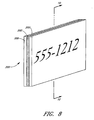
- Figure 7 illustrates a wireless telephone handset 100 having an electronic display 200.
- the electronic display 200 displays the telephone number "555-1212". It will be understood that the electronic display 200 may display other information, including, but not limited to, other text and images, either moving or static.
- the electronic display 200 can be any type of display, including, but not limited to, light emitting diode (LED), organic light emitting diode (OLED), or an interferometric modulator (IMOD) direct view electronic display.
- LED light emitting diode
- OLED organic light emitting diode
- IMOD interferometric modulator
- Embodiments of the invention relate to the manufacturing and packaging of these types of electronic displays with a desiccant.
- the packages and packaging methods described herein may be used for packaging a variety of electronic displays, including, but not limited to, the interferometric modulators described above.
- Figure 8 shows a perspective view of the display 200 from Figure 7.
- the display 200 of this embodiment has a transparent or semi-transparent front surface 250, a seal 280 and a backplane 300.
- the electronics for the particular display technology within the display 200, and between the transparent front surface 250 and backplane 300 are the electronics for the particular display technology.
- the electronics for an LED, OLED or IMOD display device within the display may be the electronics for an LED, OLED or IMOD display device. It should be realized that each of these display types has a different degree of sensitivity to moisture. Thus, it is advantageous to provide a means for reducing the amount of moisture that may come in contact with the display device.
- FIG. 9A A schematic of a basic package structure for a MEMS device, such as an interferometric modulator array, is illustrated in Figure 9A.
- a basic package structure 200 includes a substrate 250 and a backplane cover or "cap” 300, wherein an interferometric modulator array 400 is formed on the substrate 250.
- This backplane or cap 300 may also be referred to as a "backplate.”
- the terms "display,” “package structure,” and “package” may be used interchangeably, as used herein.
- the substrate 250 and the backplane 300 are joined by a seal 280 to form the package structure 200, such that the interferometric modulator array 400 is encapsulated by the substrate 250, backplane 300, and the seal 280.
- the interferometric modulator provides a
- the substrate provides a means for transmitting transmitting light therethrough.
- the backplane provides an encapsulating means for sealing the interferometric modulator within a package between the transparent substrate and the backplane
- the cavity 350 there is a cavity 350 between the backplane 300 and the substrate 250.
- the moving parts of a MEMS device such as the movable mirrors 14a, 14b of an interferometric modulator array described above, preferably have a protected space in which to move.
- the cavity 350 can be provided by the use of a backplane 300 that has a recessed cavity. Using a recessed cavity 350 allows the seal 280 to be relatively thin, and thus less subject to transmission of water vapor.
- the seal 280 is provided to join the substrate 250 and the backplane 300 to form the package structure 200.
- the seal 280 may be a non-hermetic seal, such as a conventional epoxy-based adhesive.
- the seal 280 may be a polyisobutylene (sometimes called butyl rubber, and other times PIB), o-rings, polyurethane, thin film metal weld, liquid spin-on glass, solder, polymers, or plastics, among other types of seals that may have a range of permeability of water vapor of about 0.2 - 4.7 g mm/m 2 kPa day.
- the seal 280 may be a hermetic seal.
- the substrate 250 may be a semi-transparent or transparent substance capable of having thin film, MEMS devices built upon it. Such transparent substances include, but are not limited to, glass, plastic, and transparent polymers. Images are displayed through the substrate 250, which serves as an imaging surface.
- the interferometric modulator array 400 may comprise membrane modulators or modulators of the separable type. Examples of such devices are described in U.S. Patent No. 5,835,255 to Miles.
- the backplane 300 may be formed of any suitable material, such as glass, metal, foil, polymer, plastic, ceramic, or semiconductor materials (e.g ., silicon).
- a desiccant may be used to control moisture resident within the package structure 200.
- the package structure 200 preferably includes an integrated desiccant (e.g ., desiccant integrated into the backplane material or transparent substrate material, desiccant contained within a pouch integrated with the backplane, or desiccant that is deposited or otherwise incorporated into the backplane during fabrication of the backplane) configured to reduce moisture within the cavity 350.
- a desiccant pouch 480 is positioned between the interferometric modulator array 400 and the backplane 300.
- the desiccant may also be applied to or otherwise integrated with the backplane in the recessed area(s) during fabrication of the backplane, as described in more detail below.
- Desiccants may be used for packages that have either hermetic or non-hermetic seals. In packages having a hermetic seal, desiccants are typically used to control moisture resident within the interior of the package. In packages having a non-hermetic seal, a desiccant may be used to control moisture moving into the package from the environment. The skilled artisan will appreciate that a desiccant may not be necessary for a hermetically sealed package, but may be desirable to control moisture resident within the package or to capture outgassed or residual water from epoxy or other outgassed materials or materials from surfaces inside the package.
- the desiccant preferably is configured to absorb water molecules that permeate the display package structure once it has been manufactured as well as after sealing.
- the desiccant maintains a low humidity environment within the package structure and prevents water vapor from adversely affecting the operation of the display electronics (e.g ., interferometric modulator). This maintenance of a low humidity environment will be explained more completely with reference to Figures 9-12 below.
- a desiccant pouch 480 is also sealed within the display 200.
- the desiccant pouch 480 is formed within the cavity 350 and attached to the backplane 300.
- the desiccant pouch 480 includes a desiccant material 500, and a membrane cover 550.
- the desiccant pouch 480 may be used within displays that have either hermetic or non-hermetic sealants. In displays having a hermetic seal, the desiccant pouch 480 can be used to control moisture resident within the interior of the package. In displays having a non-hermetic seal, the desiccant pouch 480 may be used to control moisture moving into the package from the surrounding environment.
- the membrane 550 of the pouch 480 preferably is made from a compound that is strong enough to contain the desiccant material 500, but also allows water vapor to pass through the membrane 550 and contact the desiccant material 500.
- a material is Tyvek® (DuPont Corporation) or polyethylene, preferably with a low moisture vapor transmission rate (MVTR).
- the MVTR of the membrane 550 depends upon the type and thickness of the materials used and the external environmental conditions. It should be realized that, in some embodiments, the membrane 550 can adhere directly to the backplane 300, 310, or be sealed to the backplane 300, 310 with an adhesive.
- Suitable adhesives include, but are not limited to, adhesives in a PSA (pressure sensitive adhesive) thin-film patch and dispensed adhesives, preferably epoxies, thermal or UV, with low outgassing specifications, such as those compliant with NASA specifications.
- PSA pressure sensitive adhesive
- dispensed adhesives preferably epoxies, thermal or UV, with low outgassing specifications, such as those compliant with NASA specifications.
- Table 1 below provides the MVTR for a number of membrane materials suitable for the membrane 550.
- the required MVTR of the membrane 550 can be calculated to ensure that the desiccant can absorb at a sufficient rate to keep the interior of the package 200, 210 dry enough for proper operation.
- any substance that can trap moisture while not interfering with the optical properties of the interferometric modulator array may be used as the desiccant material 500.
- the desiccant does not interfere with the optical properties of the interferometric modulators 400.
- Suitable desiccant materials 500 include, but are not limited to, zeolites, calcium sulfate, calcium oxide, silica gel, molecular sieves, surface adsorbents, bulk adsorbents, and chemical reactants.
- Other desiccant materials include indicating silica gel, which is silica gel with some of its granules coated with cobalt chloride. The silica changes color as it becomes saturated with water. Calcium oxide is a material that relatively slowly absorbs water.
- the desiccant material 500 may be inserted into the cavity 350 of a package structure 210 without a pouch 480 or membrane cover 550, as shown in Figure 9B.
- the backplane 310 in the embodiment shown in Figure 9B does not have as deep a recessed cavity as the backplane 300 of the embodiment shown in Figure 9A.
- the desiccant material 500 may be inserted into the cavity 350, without a pouch 480 or membrane cover 550, in a package having a backplane with a recessed cavity, such as the one shown in Figure 9A.
- the desiccant may be in different forms, shapes, and sizes.
- the desiccant material 500 may alternatively be in powder form. These powders may be inserted directly into the pouch 480 or directly into the package without a pouch 480, or they may be mixed with an adhesive for application.
- the desiccant may be formed into different shapes, such as cylinders or sheets, before being applied inside the package. It should be realized that the desiccant pouch 480 may take any form, and can be of any thickness that provides the proper desiccating function for the display 200, 210.
- the desiccant material 500 can be applied and integrated with the package in different ways.
- the desiccant material 500 is deposited as part of the interferometric modulator array 400.
- the desiccant material 500 is applied inside the package as a spray or a dip coat.
- the desiccant material 500 may be printed or sprayed onto a surface of the interior of the package, such as the backplane after it has been sandblasted or etched using standard photolithographic techniques.
- a mask is preferably first applied to the backplane prior to etching, preferably using standard photolithographic techniques, in order to form recessed pockets or windows in the backplane, allowing the package to be thinner with a thinner perimeter seal, preferably having a thickness of about 15 microns.
- etching techniques such as sandblasting and wet etching, are preferred.
- a stencil may be used instead of a photolithographic mask.
- the desiccant material 500 is applied (e.g ., sprayed or brushed on) in the recessed pockets or windows. It will be understood that the mask is preferably not removed until the desiccant material 500 has been applied to the recessed pockets or windows so that there is little danger of applying the desiccant material 500 to the non-recessed areas of the backplane.
- a thin foil may be applied over the desiccant material to protect the desiccant material 500 if the backplane is manufactured and transported prior to assembly with other parts of the package.
- the desiccant material 500 may be activated after the package is completed.
- the lifetime expectation of the device may depend on the lifetime of the desiccant.
- the interferometric modulator 400 may fail to operate as sufficient moisture enters the cavity 350 and causes damage to the interferometric modulator 400.
- the theoretical maximum lifetime of the display device is determined by the water vapor flux into the cavity 350 as well as the amount and type of desiccant material.
- the lifetime of the device is not as dependent on the desiccant capacity, or the geometry of the seal. In display devices wherein the seal 280 is not hermetic, the lifetime of the device is more dependent on the capacity of the desiccant to absorb and retain moisture.
- FIG. 10 Another embodiment of a display 580 is illustrated in Figure 10.
- two desiccant pouches 650, 700 are formed within the interior cavity 350.
- the two desiccant pouches 650, 700 function to remove moisture from within the cavity 350.
- the desiccant material 500 used to fill the pouches 650, 700 can be the same or different in the two pouches 650, 700.
- one pouch may be filled with a desiccant that binds water molecules very quickly, but wears out in a relatively short period of time.
- An example of such a desiccant is zeolite.
- the other pouch may be filled with a desiccant that absorbs water molecules more slowly, but lasts longer.
- embodiments of the invention are not limited to a particular number of integrated desiccant pouches, or a particular desiccant used within each pouch.
- the display device may have 1, 2, 3, 4, 5, 6 or more desiccant pouches inside without departing from the spirit of the invention.
- FIG. 11 Yet another embodiment of a display 780 is illustrated in Figure 11.
- the desiccant pouches 850, 950 are integrated with and adhered to the transparent or semi-transparent substrate 250 instead of to the backplane 300.
- the pouches 850, 950 do not contact or interfere with the display electronics. It should be realized that this embodiment is not limited to having desiccant pouches adhered only to the substrate 250. In other embodiments, both the substrate 250 and the backplane 300 have integrated desiccant pouches.
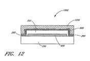
- FIG 12 shows yet another embodiment of a display 1000 wherein the desiccant material 500 is integrated into the material that forms the backplane 1050.
- the desiccant material 500 can be made by incorporating the desiccant 500 into the plastic that forms the backplane 1050.
- the desiccant is incorporated into the backplane 1050 on the internal side of the backplane 1050, as shown in Figure 12.
- Examples of such material include 2AP (Sud-Chemie), which combines precise amounts of a desiccant, such as molecular sieve or silica gel, with a polymer. Because the desiccant material 500 is incorporated into the backplane 1050 itself, there is no need to add desiccant material 500 in a separate step during the packaging process. In addition, 2AP can be customized to control the moisture adsorption rate.
- Another material suitable for a backplane 1050 is made by Capitol Specialty Plastics Inc. (Auburn, AL). This material combines a desiccant 500 with a channeling agent into a polymer that can be molded or extruded into many shapes. Almost any type of polymer can be used with the desiccant 500. This type of desiccant plastic allows the entire backplane 1050 to act as a moisture absorber.
- Other materials suitable for such a backplane 1050 include, but are not limited to, material delivered with foil protection, which can be chemically or plasma etched off, such as amorphous silicon, chrome, and similar materials.
- the packaging process to produce the display may be accomplished in a vacuum, pressure between a vacuum up to and including ambient pressure, or pressure higher than ambient pressure.
- the packaging process may also be accomplished in an environment of varied and controlled high or low pressure during the sealing process. There may be advantages to packaging the display in a completely dry environment, but it is not necessary.
- the packaging environment may be of an inert gas at ambient conditions, or the cavity 350 may be created to contain an inert gas, such as nitrogen, at ambient conditions.
- Packaging at ambient conditions allows for a lower cost process and more potential for versatility in equipment choice because the device may be transported through ambient conditions without affecting the operation of the device.
- FIGS 13A and 13B are system block diagrams illustrating an embodiment of a display device 2040.
- the display device 2040 can be, for example, a cellular or mobile telephone.
- the same components of display device 2040 or slight variations thereof are also illustrative of various types of display de vices such as televisions and portable media players.
- the display device 2040 includes a housing 2041, a display 2030, an antenna 2043, a speaker 2045, an input device 2048, and a microphone 2046.
- the housing 2041 is generally formed from any of a variety of manufacturing processes as are well known to those of skill in the art, including injection molding, and vacuum forming.
- the housing 2041 may be made from any of a variety of materials, including but not limited to plastic, metal, glass, rubber, and ceramic, or a combination thereof.
- the housing 2041 includes removable portions (not shown) that may be interchanged with other removable portions of different color, or containing different logos, pictures, or symbols.
- the display 2030 of exemplary display device 2040 may be any of a variety of displays, including a bi-stable display, as described herein.
- the display 2030 includes a flat-panel display, such as plasma, EL, OLED, STN LCD, or TFT LCD as described above, or a non-flat-panel display, such as a CRT or other tube device, as is well known to those of skill in the art.
- the display 2030 includes an interferometric modulator display, as described herein.
- the components of one embodiment of exemplary display device 2040 are schematically illustrated in Figure 13B.
- the illustrated exemplary display device 2040 includes a housing 2041 and can include additional components at least partially enclosed therein.
- the exemplary display device 2040 includes a network interface 2027 that includes an antenna 2043 which is coupled to a transceiver 2047.
- the transceiver 2047 is connected to the processor 2021, which is connected to conditioning hardware 2052.
- the conditioning hardware 2052 may be configured to condition a signal (e.g. filter a signal).
- the conditioning hardware 2052 is connected to a speaker 2045 and a microphone 2046.
- the processor 2021 is also connected to an input device 2048 and a driver controller 2029.
- the driver controller 2029 is coupled to a frame buffer 2028 and to the array driver 2022, which in turn is coupled to a display array 2030.
- a power supply 2050 provides power to all components as required by the particular exemplary display device 2040 design.
- the network interface 2027 includes the antenna 2043 and the transceiver 2047 so that the exemplary display device 2040 can communicate with one or more devices over a network. In one embodiment the network interface 2027 may also have some processing capabilities to relieve requirements of the processor 2021.
- the antenna 2043 is any antenna known to those of skill in the art for transmitting and receiving signals. In one embodiment, the antenna transmits and receives RF signals according to the IEEE 802.11 standard, including IEEE 802.11 (a), (b), or (g). In another embodiment, the antenna transmits and receives RF signals according to the BLUETOOTH standard. In the case of a cellular telephone, the antenna is designed to receive CDMA, GSM, AMPS or other known signals that are used to communicate within a wireless cell phone network.
- the transceiver 2047 pre-processes the signals received from the antenna 2043 so that they may be received by and further manipulated by the processor 2021.
- the transceiver 2047 also processes signals received from the processor 2021 so that they may be transmitted from the exemplary display device 2040 via the antenna 2043.
- the transceiver 2047 can be replaced by a receiver.
- network interface 2027 can be replaced by an image source, which can store or generate image data to be sent to the processor 2021.
- the image source can be a digital video disc (DVD) or a hard-disc drive that contains image data, or a software module that generates image data.
- Processor 2021 generally controls the overall operation of the exemplary display device 2040.
- the processor 2021 receives data, such as compressed image data from the network interface 2027 or an image source, and processes the data into raw image data or into a format that is readily processed into raw image data.
- the processor 2021 then sends the processed data to the driver controller 2029 or to frame buffer 2028 for storage.
- Raw data typically refers to the information that identifies the image characteristics at each location within an image. For example, such image characteristics can include color, saturation, and gray-scale level.
- the processor 2021 includes a microcontroller, CPU, or logic unit to control operation of the exemplary display device 2040.
- Conditioning hardware 2052 generally includes amplifiers and filters for transmitting signals to the speaker 2045, and for receiving signals from the microphone 2046.
- Conditioning hardware 2052 may be discrete components within the exemplary display device 2040, or may be incorporated within the processor 2021 or other components.
- the driver controller 2029 takes the raw image data generated by the processor 2021 either directly from the processor 2021 or from the frame buffer 2028 and reformats the raw image data appropriately for high speed transmission to the array driver 2022. Specifically, the driver controller 2029 reformats the raw image data into a data flow having a raster-like format, such that it has a time order suitable for scanning across the display array 2030. Then the driver controller 2029 sends the formatted information to the array driver 2022.
- a driver controller 2029 such as a LCD controller, is often associated with the system processor 2021 as a stand-alone Integrated Circuit (IC), such controllers may be implemented in many ways. They may be embedded in the processor 2021 as hardware, embedded in the processor 2021 as software, or fully integrated in hardware with the array driver 2022.
- IC Integrated Circuit
- the array driver 2022 receives the formatted information from the driver controller 2029 and reformats the video data into a parallel set of waveforms that are applied many times per second to the hundreds and sometimes thousands of leads coming from the display's x-y matrix of pixels.
- driver controller 2029, array driver 2022, and display array 2030 are appropriate for any of the types of displays described herein.
- driver controller 2029 is a conventional display controller or a bi-stable display controller (e.g., an interferometric modulator controller).
- array driver 2022 is a conventional driver or a bi-stable display driver (e.g., an interferometric modulator display).
- a driver controller 2029 is integrated with the array driver 2022.
- display array 2030 is a typical display array or a bi-stable display array (e.g., a display including an array of interferometric modulators).
- the input device 2048 allows a user to control the operation of the exemplary display device 2040.
- input device 2048 includes a keypad, such as a QWERTY keyboard or a telephone keypad, a button, a switch, a touch-sensitive screen, a pressure- or heat-sensitive membrane.
- the microphone 2046 is an input device for the exemplary display device 2040. When the microphone 2046 is used to input data to the device, voice commands may be provided by a user for controlling operations of the exemplary display device 2040.
- Power supply 2050 can include a variety of energy storage devices as are well known in the art.
- power supply 2050 is a rechargeable battery, such as a nickel-cadmium battery or a lithium ion battery.
- power supply 2050 is a renewable energy source, a capacitor, or a solar cell, including a plastic solar cell, and solar-cell paint.
- power supply 2050 is configured to receive power from a wall outlet.
- control programmability resides, as described above, in a driver controller which can be located in several places in the electronic display system. In some cases control programmability resides in the array driver 2022. Those of skill in the art will recognize that the above-described optimization may be implemented in any number of hardware and/or software components and in various configurations.
Abstract
Description
- The field of the invention relates to microelectromechanical systems (MEMS) and the packaging of such systems. More specifically, the field of the invention relates to interferometric modulators and methods of fabricating such modulators with a desiccant material.
- Microelectromechanical systems (MEMS) include micro mechanical elements, actuators, and electronics. Micromechanical elements may be created using deposition, etching, and or other micromachining processes that etch away parts of substrates and/or deposited material layers or that add layers to form electrical and electromechanical devices.
- One type of MEMS device is called an interferometric modulator. An interferometric modulator may comprise a pair of conductive plates, one or both of which may be transparent and/or reflective in whole or part and capable of relative motion upon application of an appropriate electrical signal. One plate may comprise a stationary layer deposited on a substrate, the other plate may comprise a metallic membrane separated from the stationary layer by an air gap. Such devices have a wide range of applications, and it would be beneficial in the art to utilize and/or modify the characteristics of these types of devices so that their features can be exploited in improving existing products and creating new products that have not yet been developed.
- The system, method, and devices of the invention each have several aspects, no single one of which is solely responsible for its desirable attributes. Without limiting the scope of this invention, its more prominent features will now be discussed briefly. After considering this discussion, and particularly after reading the section entitled "Detailed Description of Certain Embodiments" one will understand how the features of this invention provide advantages over other display devices.
- An embodiment provides a display device comprising a transparent substrate, an interferometric modulator configured to modulate light transmitted through the transparent substrate, and a backplane cover disposed on the modulator and sealing the modulator within a package between said transparent substrate and the backplane cover, wherein the backplane cover has an integrated desiccant configured to absorb moisture within the package.
- In accordance with another embodiment, a method of manufacturing a display device is provided. According to this method, a transparent substrate is provided and an interferometric modulator is formed on the transparent substrate. A backplane is then joined to the transparent substrate to form a package to encapsulate the interferometric modulator. A desiccant integrated within the package is also provided.
- According to another embodiment, a display device is provided, comprising a package, an electronic display, and a desiccant. The package comprises a transparent substrate, a backplane, and a seal applied between the backplane and the transparent substrate. The electronic display is configured to modulate light transmitted through the transparent substrate, and is formed on the transparent substrate and positioned between the transparent substrate and the backplane. The desiccant integrated into the package, and is configured to absorb moisture within the package.
- According to yet another embodiment, a display device is provided. The display device includes a transmitting means for transmitting light therethrough, a modulating means configured to modulate light transmitted through the transmitting means, an encapsulating means for sealing the modulating means within a package between the transmitting means and the encapsulating means, and a moisture absorbing means integrated into either the transmitting means or the encapsulating means.
- In another aspect, a display device is provided. The device includes transmitting means for transmitting light therethrough; modulating means configured to modulate light transmitted through the transmitting means, encapsulating means for sealing the modulating means within a package between the transmitting means and the encapsulating means, and moisture absorbing means integrated into either the transmitting means or the encapsulating means, the moisture absorbing means configured to absorb moisture through a membrane.
- According to another embodiment, a method of manufacturing a display device is provided. A transparent substrate is provided and an interferometric modulator is formed on the transparent substrate. A backplane having recessed areas on an interior surface is provided. Desiccant is applied to the recessed areas on the interior surface, and the backplane is joined to the transparent substrate to form a package after applying the desiccant.
- These and other aspects of the invention will be readily apparent from the following description and from the appended drawings (not to scale), which are meant to illustrate and not to limit the invention, and wherein:
- Figure 1 is an isometric view depicting a portion of one embodiment of an interferometric modulator display in which a movable reflective layer of a first interferometric modulator is in a released position and a movable reflective layer of a second interferometric modulator is in an actuated position.
- Figure 2 is a system block diagram illustrating one embodiment of an electronic device incorporating a 3x3 interferometric modulator display.
- Figure 3 is a diagram of movable mirror position versus applied voltage for one exemplary embodiment of an interferometric modulator of Figure 1.
- Figure 4 is an illustration of a set of row and column voltages that may be used to drive an interferometric modulator display.
- Figures 5A and 5B illustrate one exemplary timing diagram for row and column signals that may be used to write a frame of display data to the 3x3 interferometric modulator display of Figure 2.
- Figure 6A is a cross section of the device of Figure 1.
- Figure 6B is a cross section of an alternative embodiment of an interferometric modulator.
- Figure 6C is a cross section of another alternative embodiment of an interferometric modulator.
- Figure 7 schematically illustrates a front view of one embodiment of a wireless telephone handset having an electronic display.
- Figure 8 schematically illustrates a perspective view of one embodiment of an electronic display.
- Figure 9A schematically illustrates a cross-sectional view of one embodiment of an electronic display taken across the line 10-10 from Figure 8.
- Figure 9B schematically illustrates a cross-sectional view of a first alternate embodiment of an electronic display taken across the line 10-10 from Figure 8.
- Figure 10 schematically illustrates a second alternate embodiment of an electronic display taken across the line 10-10 from Figure 8.
- Figure 11 schematically illustrates a third alternate embodiment of an electronic display taken across the line 10-10 from Figure 8.
- Figure 12 schematically illustrates a fourth alternate embodiment of an electronic display taken across the line 10-10 from Figure 8 showing desiccant material integrated into the display backplane.
- Figures 13A and 13B are system block diagrams illustrating an embodiment of a visual display device comprising a plurality of interferometric modulators.
- The following detailed description is directed to certain specific embodiments of the invention. However, the invention can be embodied in a multitude of different ways. In this description, reference is made to the drawings wherein like parts are designated with like numerals throughout. As will be apparent from the following description, the invention may be implemented in any device that is configured to display an image, whether in motion (e.g., video) or stationary (e.g., still image), and whether textual or pictorial. More particularly, it is contemplated that the invention may be implemented in or associated with a variety of electronic devices such as, but not limited to, mobile telephones, wireless devices, personal data assistants (PDAs), hand-held or portable computers, GPS receivers/navigators, cameras, MP3 players, camcorders, game consoles, wrist watches, clocks, calculators, television monitors, flat panel displays, computer monitors, auto displays (e.g., odometer display, etc.), cockpit controls and/or displays, display of camera views (e.g., display of a rear view camera in a vehicle), electronic photographs, electronic billboards or signs, projectors, architectural structures, packaging, and aesthetic structures (e.g., display of images on a piece of jewelry). MEMS devices of similar structure to those described herein can also be used in non-display applications such as in electronic switching devices.
- One interferometric modulator display embodiment comprising an interferometric MEMS display element is illustrated in Figure 1. In these devices, the pixels are in either a bright or dark state. In the bright ("on" or "open") state, the display element reflects a large portion of incident visible light to a user. When in the dark ("off" or "closed") state, the display element reflects little incident visible light to the user. Depending on the embodiment, the light reflectance properties of the "on" and "off" states may be reversed. MEMS pixels can be configured to reflect predominantly at selected colors, allowing for a color display in addition to black and white.
- Figure 1 is an isometric view depicting two adjacent pixels in a series of pixels of a visual display, wherein each pixel comprises a MEMS interferometric modulator. In some embodiments, an interferometric modulator display comprises a row/column array of these interferometric modulators. Each interferometric modulator includes a pair of reflective layers positioned at a variable and controllable distance from each other to form a resonant optical cavity with at least one variable dimension. In one embodiment, one of the reflective layers may be moved between two positions. In the first position, referred to herein as the released state, the movable layer is positioned at a relatively large distance from a fixed partially reflective layer. In the second position, the movable layer is positioned more closely adjacent to the partially reflective layer. Incident light that reflects from the two layers interferes constructively or destructively depending on the position of the movable reflective layer, producing either an overall reflective or non-reflective state for each pixel.
- The depicted portion of the pixel array in Figure 1 includes two adjacent
interferometric modulators 12a and 12b. In the interferometric modulator 12a on the left, a movable and highly reflective layer 14a is illustrated in a released position at a predetermined distance from a fixed partially reflective layer 16a. In theinterferometric modulator 12b on the right, the movable highlyreflective layer 14b is illustrated in an actuated position adjacent to the fixed partiallyreflective layer 16b. - The
fixed layers 16a, 16b are electrically conductive, partially transparent and partially reflective, and may be fabricated, for example, by depositing one or more layers each of chromium and indium-tin-oxide onto atransparent substrate 20. The layers are patterned into parallel strips, and may form row electrodes in a display device as described further below. Themovable layers 14a, 14b may be formed as a series of parallel strips of a deposited metal layer or layers (orthogonal to therow electrodes 16a, 16b) deposited on top ofposts 18 and an intervening sacrificial material deposited between theposts 18. When the sacrificial material is etched away, the deformable metal layers are separated from the fixed metal layers by a definedair gap 19. A highly conductive and reflective material such as aluminum may be used for the deformable layers, and these strips may form column electrodes in a display device. - With no applied voltage, the
cavity 19 remains between the layers 14a, 16a and the deformable layer is in a mechanically relaxed state as illustrated by the pixel 12a in Figure 1. However, when a potential difference is applied to a selected row and column, the capacitor formed at the intersection of the row and column electrodes at the corresponding pixel becomes charged, and electrostatic forces pull the electrodes together. If the voltage is high enough, the movable layer is deformed and is forced against the fixed layer (a dielectric material which is not illustrated in this Figure may be deposited on the fixed layer to prevent shorting and control the separation distance) as illustrated by thepixel 12b on the right in Figure 1. The behavior is the same regardless of the polarity of the applied potential difference. In this way, row/column actuation that can control the reflective vs. non-reflective pixel states is analogous in many ways to that used in conventional LCD and other display technologies. - Figures 2 through 5 illustrate one exemplary process and system for using an array of interferometric modulators in a display application. Figure 2 is a system block diagram illustrating one embodiment of an electronic device that may incorporate aspects of the invention. In the exemplary embodiment, the electronic device includes a
processor 21 which may be any general purpose single- or multi-chip microprocessor such as an ARM, Pentium®, Pentium II®, Pentium III®, Pentium IV®, Pentium® Pro, an 8051, a MIPS®, a Power PC®, an ALPHA®, or any special purpose microprocessor such as a digital signal processor, microcontroller, or a programmable gate array. As is conventional in the art, theprocessor 21 may be configured to execute one or more software modules. In addition to executing an operating system, the processor may be configured to execute one or more software applications, including a web browser, a telephone application, an email program, or any other software application. - In one embodiment, the
processor 21 is also configured to communicate with anarray controller 22. In one embodiment, thearray controller 22 includes arow driver circuit 24 and acolumn driver circuit 26 that provide signals to apixel array 30. The cross section of the array illustrated in Figure 1 is shown by the lines 1-1 in Figure 2. For MEMS interferometric modulators, the row/column actuation protocol may take advantage of a hysteresis property of these devices illustrated in Figure 3. It may require, for example, a 10 volt potential difference to cause a movable layer to deform from the released state to the actuated state. However, when the voltage is reduced from that value, the movable layer maintains its state as the voltage drops back below 10 volts. In the exemplary embodiment of Figure 3, the movable layer does not release completely until the voltage drops below 2 volts. There is thus a range of voltage, about 3 to 7 V in the example illustrated in Figure 3, where there exists a window of applied voltage within which the device is stable in either the released or actuated state. This is referred to herein as the "hysteresis window" or "stability window." For a display array having the hysteresis characteristics of Figure 3, the row/column actuation protocol can be designed such that during row strobing, pixels in the strobed row that are to be actuated are exposed to a voltage difference of about 10 volts, and pixels that are to be released are exposed to a voltage difference of close to zero volts. After the strobe, the pixels are exposed to a steady state voltage difference of about 5 volts such that they remain in whatever state the row strobe put them in. After being written, each pixel sees a potential difference within the "stability window" of 3-7 volts in this example. This feature makes the pixel design illustrated in Figure 1 stable under the same applied voltage conditions in either an actuated or released pre-existing state. Since each pixel of the interferometric modulator, whether in the actuated or released state, is essentially a capacitor formed by the fixed and moving reflective layers, this stable state can be held at a voltage within the hysteresis window with almost no power dissipation. Essentially no current flows into the pixel if the applied potential is fixed. - In typical applications, a display frame may be created by asserting the set of column electrodes in accordance with the desired set of actuated pixels in the first row. A row pulse is then applied to the
row 1 electrode, actuating the pixels corresponding to the asserted column lines. The asserted set of column electrodes is then changed to correspond to the desired set of actuated pixels in the second row. A pulse is then applied to therow 2 electrode, actuating the appropriate pixels inrow 2 in accordance with the asserted column electrodes. Therow 1 pixels are unaffected by therow 2 pulse, and remain in the state they were set to during therow 1 pulse. This may be repeated for the entire series of rows in a sequential fashion to produce the frame. Generally, the frames are refreshed and/or updated with new display data by continually repeating this process at some desired number of frames per second. A wide variety of protocols for driving row and column electrodes of pixel arrays to produce display frames are also well known and may be used in conjunction with the present invention. - Figures 4 and 5 illustrate one possible actuation protocol for creating a display frame on the 3x3 array of Figure 2. Figure 4 illustrates a possible set of column and row voltage levels that may be used for pixels exhibiting the hysteresis curves of Figure 3. In the Figure 4 embodiment, actuating a pixel involves setting the appropriate column to -Vbias, and the appropriate row to +ΔV, which may correspond to -5 volts and +5 volts respectively Releasing the pixel is accomplished by setting the appropriate column to +Vbias, and the appropriate row to the same +ΔV, producing a zero volt potential difference across the pixel. In those rows where the row voltage is held at zero volts, the pixels are stable in whatever state they were originally in, regardless of whether the column is at +Vbias, or -Vbias.
- Figure 5B is a timing diagram showing a series of row and column signals applied to the 3x3 array of Figure 2 which will result in the display arrangement illustrated in Figure 5A, where actuated pixels are non-reflective. Prior to writing the frame illustrated in Figure 5A, the pixels can be in any state, and in this example, all the rows are at 0 volts, and all the columns are at +5 volts. With these applied voltages, all pixels are stable in their existing actuated or released states.
- In the Figure 5A frame, pixels (1,1), (1,2), (2,2), (3,2) and (3,3) are actuated. To accomplish this, during a "line time" for
row 1,columns column 3 is set to +5 volts. This does not change the state of any pixels, because all the pixels remain in the 3-7 volt stability window.Row 1 is then strobed with a pulse that goes from 0, up to 5 volts, and back to zero. This actuates the (1,1) and (1,2) pixels and releases the (1,3) pixel. No other pixels in the array are affected. To setrow 2 as desired,column 2 is set to -5 volts, andcolumns Row 3 is similarly set by settingcolumns column 1 to +5 volts. Therow 3 strobe sets therow 3 pixels as shown in Figure 5A. After writing the frame, the row potentials are zero, and the column potentials can remain at either +5 or -5 volts, and the display is then stable in the arrangement of Figure 5A. It will be appreciated that the same procedure can be employed for arrays of dozens or hundreds of rows and columns. It will also be appreciated that the timing, sequence, and levels of voltages used to perform row and column actuation can be varied widely within the general principles outlined above, and the above example is exemplary only, and any actuation voltage method can be used with the present invention. - The details of the structure of interferometric modulators that operate in accordance with the principles set forth above may vary widely. For example, Figures 6A-6C illustrate three different embodiments of the moving mirror structure. Figure 6A is a cross section of the embodiment of Figure 1, where a strip of
metal material 14 is deposited on orthogonally extending supports 18. In Figure 6B, the moveablereflective material 14 is attached to supports at the corners only, on tethers 32. In Figure 6C, the moveablereflective material 14 is suspended from a deformable layer 34. This embodiment has benefits because the structural design and materials used for thereflective material 14 can be optimized with respect to the optical properties, and the structural design and materials used for the deformable layer 34 can be optimized with respect to desired mechanical properties. The production of various types of interferometric devices is described in a variety of published documents, including, for example, U.S. Published Application 2004/0051929. A wide variety of well known techniques may be used to produce the above described structures involving a series of material deposition, patterning, and etching steps. - Figure 7 illustrates a wireless telephone handset 100 having an
electronic display 200. In this illustration, theelectronic display 200 displays the telephone number "555-1212". It will be understood that theelectronic display 200 may display other information, including, but not limited to, other text and images, either moving or static. - The
electronic display 200 can be any type of display, including, but not limited to, light emitting diode (LED), organic light emitting diode (OLED), or an interferometric modulator (IMOD) direct view electronic display. Embodiments of the invention relate to the manufacturing and packaging of these types of electronic displays with a desiccant. The packages and packaging methods described herein may be used for packaging a variety of electronic displays, including, but not limited to, the interferometric modulators described above. - Figure 8 shows a perspective view of the
display 200 from Figure 7. As shown in Figure 8, thedisplay 200 of this embodiment has a transparent or semi-transparentfront surface 250, aseal 280 and abackplane 300. As will be explained below, within thedisplay 200, and between the transparentfront surface 250 andbackplane 300 are the electronics for the particular display technology. For example, within the display may be the electronics for an LED, OLED or IMOD display device. It should be realized that each of these display types has a different degree of sensitivity to moisture. Thus, it is advantageous to provide a means for reducing the amount of moisture that may come in contact with the display device. - Packaging techniques for a MEMS device will be described in more detail below. A schematic of a basic package structure for a MEMS device, such as an interferometric modulator array, is illustrated in Figure 9A. As shown in Figure 9A, a
basic package structure 200 includes asubstrate 250 and a backplane cover or "cap" 300, wherein aninterferometric modulator array 400 is formed on thesubstrate 250. This backplane orcap 300 may also be referred to as a "backplate." It will be understood that the terms "display," "package structure," and "package" may be used interchangeably, as used herein. - According to the embodiment shown in Figure 9A, the
substrate 250 and thebackplane 300 are joined by aseal 280 to form thepackage structure 200, such that theinterferometric modulator array 400 is encapsulated by thesubstrate 250,backplane 300, and theseal 280. The interferometric modulator provides a The substrate provides a means for transmitting transmitting light therethrough. The backplane provides an encapsulating means for sealing the interferometric modulator within a package between the transparent substrate and the backplane - As shown in Figure 9A, there is a
cavity 350 between thebackplane 300 and thesubstrate 250. The moving parts of a MEMS device, such as themovable mirrors 14a, 14b of an interferometric modulator array described above, preferably have a protected space in which to move. As illustrated in Figure 9A, thecavity 350 can be provided by the use of abackplane 300 that has a recessed cavity. Using a recessedcavity 350 allows theseal 280 to be relatively thin, and thus less subject to transmission of water vapor. - The
seal 280 is provided to join thesubstrate 250 and thebackplane 300 to form thepackage structure 200. Theseal 280 may be a non-hermetic seal, such as a conventional epoxy-based adhesive. In other embodiments, theseal 280 may be a polyisobutylene (sometimes called butyl rubber, and other times PIB), o-rings, polyurethane, thin film metal weld, liquid spin-on glass, solder, polymers, or plastics, among other types of seals that may have a range of permeability of water vapor of about 0.2 - 4.7 g mm/m2kPa day. In still other embodiments, theseal 280 may be a hermetic seal. - The
substrate 250 may be a semi-transparent or transparent substance capable of having thin film, MEMS devices built upon it. Such transparent substances include, but are not limited to, glass, plastic, and transparent polymers. Images are displayed through thesubstrate 250, which serves as an imaging surface. Theinterferometric modulator array 400 may comprise membrane modulators or modulators of the separable type. Examples of such devices are described in U.S. Patent No. 5,835,255 to Miles. The skilled artisan will appreciate that thebackplane 300 may be formed of any suitable material, such as glass, metal, foil, polymer, plastic, ceramic, or semiconductor materials (e.g., silicon). - Generally, it is desirable to minimize the permeation of water vapor into the package structure and thus control the environment inside the
package structure 200 and hermetically seal it to ensure that the environment remains constant. An example of a hermetic sealing process is disclosed in U.S. Patent No. 6,589,625. When the humidity within thepackage structure 200 exceeds a level beyond which surface tension from the moisture becomes higher than the restoration force of a movable element (e.g., themovable mirrors 14a, 14b described above) in theinterferometric modulator 400, the movable element may become permanently stuck to the surface. - A desiccant may be used to control moisture resident within the
package structure 200. Thepackage structure 200 preferably includes an integrated desiccant (e.g., desiccant integrated into the backplane material or transparent substrate material, desiccant contained within a pouch integrated with the backplane, or desiccant that is deposited or otherwise incorporated into the backplane during fabrication of the backplane) configured to reduce moisture within thecavity 350. In the embodiment shown in Figure 9A, adesiccant pouch 480 is positioned between theinterferometric modulator array 400 and thebackplane 300. The desiccant may also be applied to or otherwise integrated with the backplane in the recessed area(s) during fabrication of the backplane, as described in more detail below. - Desiccants may be used for packages that have either hermetic or non-hermetic seals. In packages having a hermetic seal, desiccants are typically used to control moisture resident within the interior of the package. In packages having a non-hermetic seal, a desiccant may be used to control moisture moving into the package from the environment. The skilled artisan will appreciate that a desiccant may not be necessary for a hermetically sealed package, but may be desirable to control moisture resident within the package or to capture outgassed or residual water from epoxy or other outgassed materials or materials from surfaces inside the package.
- According to the embodiments described herein, the desiccant preferably is configured to absorb water molecules that permeate the display package structure once it has been manufactured as well as after sealing. As can be appreciated, the desiccant maintains a low humidity environment within the package structure and prevents water vapor from adversely affecting the operation of the display electronics (e.g., interferometric modulator). This maintenance of a low humidity environment will be explained more completely with reference to Figures 9-12 below.
- As illustrated in Figure 9A, also sealed within the
display 200 is adesiccant pouch 480. In these embodiments, thedesiccant pouch 480 is formed within thecavity 350 and attached to thebackplane 300. Thedesiccant pouch 480 includes adesiccant material 500, and amembrane cover 550. Thedesiccant pouch 480 may be used within displays that have either hermetic or non-hermetic sealants. In displays having a hermetic seal, thedesiccant pouch 480 can be used to control moisture resident within the interior of the package. In displays having a non-hermetic seal, thedesiccant pouch 480 may be used to control moisture moving into the package from the surrounding environment. - The
membrane 550 of thepouch 480 preferably is made from a compound that is strong enough to contain thedesiccant material 500, but also allows water vapor to pass through themembrane 550 and contact thedesiccant material 500. An example of such a material is Tyvek® (DuPont Corporation) or polyethylene, preferably with a low moisture vapor transmission rate (MVTR). The MVTR of themembrane 550 depends upon the type and thickness of the materials used and the external environmental conditions. It should be realized that, in some embodiments, themembrane 550 can adhere directly to thebackplane backplane - Table 1 below provides the MVTR for a number of membrane materials suitable for the
membrane 550. By knowing the MVTR (in grams of water per square foot per day), the total surface area of the membrane 550 (membrane surface area) and the rate of water permeation into thepackage membrane 550 can be calculated to ensure that the desiccant can absorb at a sufficient rate to keep the interior of thepackage Table 1 Material MVTR* gm/m 2 -day gm/ft 2 -day Aluminum Foil Wrapping 0.025 mm 0.5 0.05 Aluminum Foil Wrapping 0.009mm 1.0 0.09 Cellulose Films ('Cellophane') 400's MXXT Grade (Polyvinylidene Chloride Coated) Polyvinylidene/Polyvinyl Chloride Films ('Saran') 0.005 cm (0.002 in) 1.5 0.14 Polyvinylidene/Polyvinyl Chloride Films ('Saran') 0.0013 cm (0.0005 in) 3.0 0.28 Polyethylene Films ('Polythene') 0.0125cm (0.005in) Waxed Paper (45.5 kg (100 lb) per DC Ream) 4.0 0.37 Cellulose Films ('Cellophane') 300's MSAT Grade (Cellulose Nitrate Coated) 7.5 0.70 Glassine Lacquered (16 kg (35 lb) per DC Ream) 9.0 0.84 Polyethylene Film ('Polythene') 0.005 cm (0.002) in) 10.0 0.93 Polyethylene Film ('Polythene') 0.0025 cm (0.001 in) 20.0 1.86 Polyethylene Coated Kraft (9kg (20 lb) per DC Ream) 30.0 2.79 *Determined at 100°F and 90% relative humidity - Generally, any substance that can trap moisture while not interfering with the optical properties of the interferometric modulator array may be used as the
desiccant material 500. Preferably, the desiccant does not interfere with the optical properties of theinterferometric modulators 400.Suitable desiccant materials 500 include, but are not limited to, zeolites, calcium sulfate, calcium oxide, silica gel, molecular sieves, surface adsorbents, bulk adsorbents, and chemical reactants. Other desiccant materials include indicating silica gel, which is silica gel with some of its granules coated with cobalt chloride. The silica changes color as it becomes saturated with water. Calcium oxide is a material that relatively slowly absorbs water. - It will be understood that, in certain embodiments, the
desiccant material 500 may be inserted into thecavity 350 of apackage structure 210 without apouch 480 ormembrane cover 550, as shown in Figure 9B. Thebackplane 310 in the embodiment shown in Figure 9B does not have as deep a recessed cavity as thebackplane 300 of the embodiment shown in Figure 9A. The skilled artisan will appreciate that thedesiccant material 500 may be inserted into thecavity 350, without apouch 480 ormembrane cover 550, in a package having a backplane with a recessed cavity, such as the one shown in Figure 9A. - The desiccant may be in different forms, shapes, and sizes. In addition to being in solid or gel form, the
desiccant material 500 may alternatively be in powder form. These powders may be inserted directly into thepouch 480 or directly into the package without apouch 480, or they may be mixed with an adhesive for application. In an alternative embodiment, the desiccant may be formed into different shapes, such as cylinders or sheets, before being applied inside the package. It should be realized that thedesiccant pouch 480 may take any form, and can be of any thickness that provides the proper desiccating function for thedisplay - The skilled artisan will understand that the
desiccant material 500 can be applied and integrated with the package in different ways. In one embodiment, thedesiccant material 500 is deposited as part of theinterferometric modulator array 400. In another embodiment, thedesiccant material 500 is applied inside the package as a spray or a dip coat. - In another embodiment, the
desiccant material 500 may be printed or sprayed onto a surface of the interior of the package, such as the backplane after it has been sandblasted or etched using standard photolithographic techniques. A mask is preferably first applied to the backplane prior to etching, preferably using standard photolithographic techniques, in order to form recessed pockets or windows in the backplane, allowing the package to be thinner with a thinner perimeter seal, preferably having a thickness of about 15 microns. The skilled artisan will also appreciate that a thinned perimeter seal allows lower water vapor flux into the package and the package/device would therefore have a longer lifetime. It will be understood that etching techniques, such as sandblasting and wet etching, are preferred. The skilled artisan will understand that, alternatively, a stencil may be used instead of a photolithographic mask. After the pockets or windows have been created, thedesiccant material 500 is applied (e.g., sprayed or brushed on) in the recessed pockets or windows. It will be understood that the mask is preferably not removed until thedesiccant material 500 has been applied to the recessed pockets or windows so that there is little danger of applying thedesiccant material 500 to the non-recessed areas of the backplane. A thin foil may be applied over the desiccant material to protect thedesiccant material 500 if the backplane is manufactured and transported prior to assembly with other parts of the package. Thedesiccant material 500 may be activated after the package is completed. - Typically, in packages containing desiccants, the lifetime expectation of the device may depend on the lifetime of the desiccant. When the desiccant is fully consumed, the
interferometric modulator 400 may fail to operate as sufficient moisture enters thecavity 350 and causes damage to theinterferometric modulator 400. The theoretical maximum lifetime of the display device is determined by the water vapor flux into thecavity 350 as well as the amount and type of desiccant material. The theoretical lifetime of the device may be calculated with the following equations:

where P is the water vapor permeation coefficient for theperimeter seal 280 and
seal 280. - In the embodiment of a display having a hermetic seal, the lifetime of the device is not as dependent on the desiccant capacity, or the geometry of the seal. In display devices wherein the
seal 280 is not hermetic, the lifetime of the device is more dependent on the capacity of the desiccant to absorb and retain moisture. - Another embodiment of a
display 580 is illustrated in Figure 10. As shown, twodesiccant pouches interior cavity 350. The twodesiccant pouches cavity 350. It should be realized that, in this embodiment, thedesiccant material 500 used to fill thepouches pouches - Yet another embodiment of a
display 780 is illustrated in Figure 11. In this embodiment, thedesiccant pouches semi-transparent substrate 250 instead of to thebackplane 300. Preferably, thepouches substrate 250. In other embodiments, both thesubstrate 250 and thebackplane 300 have integrated desiccant pouches. - Figure 12 shows yet another embodiment of a
display 1000 wherein thedesiccant material 500 is integrated into the material that forms thebackplane 1050. Such material can be made by incorporating thedesiccant 500 into the plastic that forms thebackplane 1050. Preferably, the desiccant is incorporated into thebackplane 1050 on the internal side of thebackplane 1050, as shown in Figure 12. Examples of such material include 2AP (Sud-Chemie), which combines precise amounts of a desiccant, such as molecular sieve or silica gel, with a polymer. Because thedesiccant material 500 is incorporated into thebackplane 1050 itself, there is no need to adddesiccant material 500 in a separate step during the packaging process. In addition, 2AP can be customized to control the moisture adsorption rate. - Another material suitable for a
backplane 1050 is made by Capitol Specialty Plastics Inc. (Auburn, AL). This material combines adesiccant 500 with a channeling agent into a polymer that can be molded or extruded into many shapes. Almost any type of polymer can be used with thedesiccant 500. This type of desiccant plastic allows theentire backplane 1050 to act as a moisture absorber. Other materials suitable for such abackplane 1050 include, but are not limited to, material delivered with foil protection, which can be chemically or plasma etched off, such as amorphous silicon, chrome, and similar materials. - Generally, the packaging process to produce the display may be accomplished in a vacuum, pressure between a vacuum up to and including ambient pressure, or pressure higher than ambient pressure. The packaging process may also be accomplished in an environment of varied and controlled high or low pressure during the sealing process. There may be advantages to packaging the display in a completely dry environment, but it is not necessary. Similarly, the packaging environment may be of an inert gas at ambient conditions, or the
cavity 350 may be created to contain an inert gas, such as nitrogen, at ambient conditions. Packaging at ambient conditions allows for a lower cost process and more potential for versatility in equipment choice because the device may be transported through ambient conditions without affecting the operation of the device. - Figures 13A and 13B are system block diagrams illustrating an embodiment of a
display device 2040. Thedisplay device 2040 can be, for example, a cellular or mobile telephone. However, the same components ofdisplay device 2040 or slight variations thereof are also illustrative of various types of display de vices such as televisions and portable media players. - The
display device 2040 includes ahousing 2041, adisplay 2030, anantenna 2043, aspeaker 2045, aninput device 2048, and amicrophone 2046. Thehousing 2041 is generally formed from any of a variety of manufacturing processes as are well known to those of skill in the art, including injection molding, and vacuum forming. In addition, thehousing 2041 may be made from any of a variety of materials, including but not limited to plastic, metal, glass, rubber, and ceramic, or a combination thereof. In one embodiment thehousing 2041 includes removable portions (not shown) that may be interchanged with other removable portions of different color, or containing different logos, pictures, or symbols. - The
display 2030 ofexemplary display device 2040 may be any of a variety of displays, including a bi-stable display, as described herein. In other embodiments, thedisplay 2030 includes a flat-panel display, such as plasma, EL, OLED, STN LCD, or TFT LCD as described above, or a non-flat-panel display, such as a CRT or other tube device, as is well known to those of skill in the art. However, for purposes of describing the present embodiment, thedisplay 2030 includes an interferometric modulator display, as described herein. - The components of one embodiment of
exemplary display device 2040 are schematically illustrated in Figure 13B. The illustratedexemplary display device 2040 includes ahousing 2041 and can include additional components at least partially enclosed therein. For example, in one embodiment, theexemplary display device 2040 includes anetwork interface 2027 that includes anantenna 2043 which is coupled to atransceiver 2047. Thetransceiver 2047 is connected to theprocessor 2021, which is connected toconditioning hardware 2052. Theconditioning hardware 2052 may be configured to condition a signal (e.g. filter a signal). Theconditioning hardware 2052 is connected to aspeaker 2045 and amicrophone 2046. Theprocessor 2021 is also connected to aninput device 2048 and adriver controller 2029. Thedriver controller 2029 is coupled to aframe buffer 2028 and to thearray driver 2022, which in turn is coupled to adisplay array 2030. Apower supply 2050 provides power to all components as required by the particularexemplary display device 2040 design. - The
network interface 2027 includes theantenna 2043 and thetransceiver 2047 so that theexemplary display device 2040 can communicate with one or more devices over a network. In one embodiment thenetwork interface 2027 may also have some processing capabilities to relieve requirements of theprocessor 2021. Theantenna 2043 is any antenna known to those of skill in the art for transmitting and receiving signals. In one embodiment, the antenna transmits and receives RF signals according to the IEEE 802.11 standard, including IEEE 802.11 (a), (b), or (g). In another embodiment, the antenna transmits and receives RF signals according to the BLUETOOTH standard. In the case of a cellular telephone, the antenna is designed to receive CDMA, GSM, AMPS or other known signals that are used to communicate within a wireless cell phone network. Thetransceiver 2047 pre-processes the signals received from theantenna 2043 so that they may be received by and further manipulated by theprocessor 2021. Thetransceiver 2047 also processes signals received from theprocessor 2021 so that they may be transmitted from theexemplary display device 2040 via theantenna 2043. - In an alternative embodiment, the
transceiver 2047 can be replaced by a receiver. In yet another alternative embodiment,network interface 2027 can be replaced by an image source, which can store or generate image data to be sent to theprocessor 2021. For example, the image source can be a digital video disc (DVD) or a hard-disc drive that contains image data, or a software module that generates image data. -
Processor 2021 generally controls the overall operation of theexemplary display device 2040. Theprocessor 2021 receives data, such as compressed image data from thenetwork interface 2027 or an image source, and processes the data into raw image data or into a format that is readily processed into raw image data. Theprocessor 2021 then sends the processed data to thedriver controller 2029 or to framebuffer 2028 for storage. Raw data typically refers to the information that identifies the image characteristics at each location within an image. For example, such image characteristics can include color, saturation, and gray-scale level. - In one embodiment, the
processor 2021 includes a microcontroller, CPU, or logic unit to control operation of theexemplary display device 2040.Conditioning hardware 2052 generally includes amplifiers and filters for transmitting signals to thespeaker 2045, and for receiving signals from themicrophone 2046.Conditioning hardware 2052 may be discrete components within theexemplary display device 2040, or may be incorporated within theprocessor 2021 or other components. - The
driver controller 2029 takes the raw image data generated by theprocessor 2021 either directly from theprocessor 2021 or from theframe buffer 2028 and reformats the raw image data appropriately for high speed transmission to thearray driver 2022. Specifically, thedriver controller 2029 reformats the raw image data into a data flow having a raster-like format, such that it has a time order suitable for scanning across thedisplay array 2030. Then thedriver controller 2029 sends the formatted information to thearray driver 2022. Although adriver controller 2029, such as a LCD controller, is often associated with thesystem processor 2021 as a stand-alone Integrated Circuit (IC), such controllers may be implemented in many ways. They may be embedded in theprocessor 2021 as hardware, embedded in theprocessor 2021 as software, or fully integrated in hardware with thearray driver 2022. - Typically, the
array driver 2022 receives the formatted information from thedriver controller 2029 and reformats the video data into a parallel set of waveforms that are applied many times per second to the hundreds and sometimes thousands of leads coming from the display's x-y matrix of pixels. - In one embodiment, the
driver controller 2029,array driver 2022, anddisplay array 2030 are appropriate for any of the types of displays described herein. For example, in one embodiment,driver controller 2029 is a conventional display controller or a bi-stable display controller (e.g., an interferometric modulator controller). In another embodiment,array driver 2022 is a conventional driver or a bi-stable display driver (e.g., an interferometric modulator display). In one embodiment, adriver controller 2029 is integrated with thearray driver 2022. Such an embodiment is common in highly integrated systems such as cellular phones, watches, and other small area displays. In yet another embodiment,display array 2030 is a typical display array or a bi-stable display array (e.g., a display including an array of interferometric modulators). - The
input device 2048 allows a user to control the operation of theexemplary display device 2040. In one embodiment,input device 2048 includes a keypad, such as a QWERTY keyboard or a telephone keypad, a button, a switch, a touch-sensitive screen, a pressure- or heat-sensitive membrane. In one embodiment, themicrophone 2046 is an input device for theexemplary display device 2040. When themicrophone 2046 is used to input data to the device, voice commands may be provided by a user for controlling operations of theexemplary display device 2040. -
Power supply 2050 can include a variety of energy storage devices as are well known in the art. For example, in one embodiment,power supply 2050 is a rechargeable battery, such as a nickel-cadmium battery or a lithium ion battery. In another embodiment,power supply 2050 is a renewable energy source, a capacitor, or a solar cell, including a plastic solar cell, and solar-cell paint. In another embodiment,power supply 2050 is configured to receive power from a wall outlet. - In some implementations control programmability resides, as described above, in a driver controller which can be located in several places in the electronic display system. In some cases control programmability resides in the
array driver 2022. Those of skill in the art will recognize that the above-described optimization may be implemented in any number of hardware and/or software components and in various configurations. - While the above detailed description has shown, described, and pointed out novel features of the invention as applied to various embodiments, it will be understood that various omissions, substitutions, and changes in the form and details of the device or process illustrated may be made by those skilled in the art without departing from the spirit of the invention. As will be recognized, the present invention may be embodied within a form that does not provide all of the features and benefits set forth herein, as some features may be used or practiced separately from others.
Claims (38)
- A method of manufacturing a display device, comprising:providing a transparent substrate comprising an interferometric modulator;forming a backplane comprising an integrated desiccant; andjoining the backplane to the transparent substrate.
- The method of Claim 1, wherein the backplane comprises a polymer and one of a molecular sieve or silica gel.
- The method of Claim 1, wherein the backplane comprises a desiccant, a channeling agent, and a polymer.
- The method of Claim 1, wherein forming the backplane comprises molding or extruding the backplane.
- The method of Claim 1, wherein the at least one integrated desiccant comprises at least one of zeolites, calcium sulfate, calcium oxide, silica gel, molecular sieves, surface adsorbents, bulk adsorbents, chemical reactants, and indicating silica gel.
- The method of Claim 1, wherein forming a backplane comprises creating a recessed area in said backplane and applying a desiccant to said recessed area.
- A display device made by the method of any one of Claims 1 to 6.
- A display device, comprising:transmitting means for transmitting light therethrough;modulating means configured to modulate light transmitted through the transmitting means;encapsulating means for sealing the modulating means within a package between the transmitting means and the encapsulating means; andmoisture absorbing means integrated into either the transmitting means or the encapsulating means.
- The display device of Claim 8, wherein the moisture absorbing means is a dessicant.
- The display device of Claim 9, wherein said dessicant comprises at least one of zeolites, calcium sulfate, calcium oxide, silica gel, molecular sieves, surface adsorbents, bulk adsorbents, chemical reactants, and indicating silica gel.
- The display device of Claim 8, wherein the encapsulating means is formed of a material comprising the moisture absorbing means.
- The display device of Claim 10, wherein the encapsulating means comprises a polymer and one of a molecular sieve or silica gel.
- The display device of Claim 11, wherein the encapsulating means comprises a polymer and the moisture absorbing means comprises a desiccant and a channeling agent.
- The display device of Claim 8, wherein the moisture absorbing means is applied to a surface of the encapsulating means as a spray coat.
- The display device of Claim 8, wherein the encapsulating means comprises a backplane comprising a recessed portion, and the recessed portion comprises the moisture absorbing means.
- The display device of Claim 8, wherein the moisture absorbing means comprises at least one of zeolites, calcium sulfate, calcium oxide, silica gel, molecular sieves, surface adsorbents, bulk adsorbents, chemical reactants, and indicating silica gel.
- A method of manufacturing an electronic device, comprising:providing a transparent substrate comprising an interferometric modulator;providing a backplane; andapplying a desiccant to the transparent substrate or the backplane, wherein a membrane at least partially covers the desiccant; andsealing the transparent substrate to the backplane.
- The method of Claim 17, wherein the membrane is adhered to the backplane.
- The method of Claim 17, wherein the membrane is adhered to the transparent substrate.
- The method of Claim 17, wherein the membrane is formed of polyethylene.
- The method of Claim 17, wherein the at least one desiccant comprises at least one of zeolites, calcium sulfate, calcium oxide, silica gel, molecular sieves, surface adsorbents, bulk adsorbents, chemical reactants, and indicating silica gel.
- The method of Claim 17, wherein the transparent substrate is glass.
- An electronic device manufactured by the method of any one of claims 17 to 22.
- The electronic device of Claim 23, wherein said device is an interferometric modulator.
- A display device, comprising:transmitting means for transmitting light therethrough;modulating means configured to modulate light transmitted through the transmitting means;encapsulating means for sealing the modulating means within a package between the transmitting means and the encapsulating means; andmoisture absorbing means in contact with either the transmitting means or the encapsulating means, the moisture absorbing means being configured to absorb moisture through a membrane.
- The display device of Claim 25, wherein the moisture absorbing means comprises a dessicant.
- The display device of Claim 26, wherein the at least one dessicant comprises at least one of zeolites, calcium sulfate, calcium oxide, silica gel, molecular sieves, surface adsorbents, bulk adsorbents, chemical reactants, and indicating silica gel.
- The display device of Claim 8, 9, 25 or 26, wherein the encapsulating means comprises a backplane.
- The display device of Claim 8, 9, 24, 25, or 28, wherein the modulating means comprises an interferometric modulator.
- The display device of Claim 8, 9 or any one of Claims 25 to 29, wherein the transmitting means comprises a transparent substrate.
- The display device of Claim 25, wherein the moisture absorbing means comprises a pouch of desiccant adhered to the encapsulating means.
- The display device of Claim 25, wherein the moisture absorbing means comprises a pouch of desiccant adhered to the transmitting means.
- The display device of Claims 29, further comprising:a processor that is in electrical communication with said interferometric modulator, said processor being configured to process image data; anda memory device in electrical communication with said processor.
- The display device of Claim 33, further comprising a driver circuit configured to send at least one signal to said interferometric modulator.
- The display device of Claim 34, further comprising a controller configured to send at least a portion of said image data to said driver circuit.
- The display device of Claim 33, further comprising an image source module configured to send said image data to said processor.
- The display device of Claim 36, wherein said image source module comprises at least one of a receiver, transceiver, and transmitter.
- The display device of Claim 33, further comprising an input device configured to receive input data and to communicate said input data to said processor.
Applications Claiming Priority (2)
| Application Number | Priority Date | Filing Date | Title |
|---|---|---|---|
| US61330004P | 2004-09-27 | 2004-09-27 | |
| US11/107,518 US7551246B2 (en) | 2004-09-27 | 2005-04-15 | System and method for display device with integrated desiccant |
Publications (2)
| Publication Number | Publication Date |
|---|---|
| EP1640324A2 true EP1640324A2 (en) | 2006-03-29 |
| EP1640324A3 EP1640324A3 (en) | 2008-04-09 |
Family
ID=35462141
Family Applications (1)
| Application Number | Title | Priority Date | Filing Date |
|---|---|---|---|
| EP05255658A Withdrawn EP1640324A3 (en) | 2004-09-27 | 2005-09-14 | System and method for display device with integrated desiccant |
Country Status (12)
| Country | Link |
|---|---|
| US (1) | US7551246B2 (en) |
| EP (1) | EP1640324A3 (en) |
| JP (1) | JP2006099065A (en) |
| KR (1) | KR101199903B1 (en) |
| CN (1) | CN102358609A (en) |
| AU (1) | AU2005203379A1 (en) |
| BR (1) | BRPI0503936A (en) |
| CA (1) | CA2516912A1 (en) |
| MX (1) | MXPA05009404A (en) |
| RU (1) | RU2005129924A (en) |
| SG (1) | SG121055A1 (en) |
| TW (1) | TW200626473A (en) |
Cited By (5)
| Publication number | Priority date | Publication date | Assignee | Title |
|---|---|---|---|---|
| WO2007136706A1 (en) * | 2006-05-17 | 2007-11-29 | Qualcomm Mems Technologies Inc. | Desiccant in a mems device |
| WO2008006651A1 (en) * | 2006-07-10 | 2008-01-17 | Robert Bosch Gmbh | Method for producing a sensor element and sensor element |
| WO2008069882A2 (en) * | 2006-12-01 | 2008-06-12 | Qualcomm Mems Technologies, Inc. | Mems processing with additional baking for contaminant removal |
| CN104656300A (en) * | 2015-02-12 | 2015-05-27 | 苏州佳世达电通有限公司 | Dew removing method |
| EP2155582B1 (en) | 2007-05-07 | 2015-07-29 | Clariant Production (France) S.A.S. | Container with moisture control capacity |
Families Citing this family (27)
| Publication number | Priority date | Publication date | Assignee | Title |
|---|---|---|---|---|
| US8110260B2 (en) | 2007-02-02 | 2012-02-07 | Rick Merical | Containers intended for moisture-sensitive products |
| US8003179B2 (en) | 2002-06-20 | 2011-08-23 | Alcan Packaging Flexible France | Films having a desiccant material incorporated therein and methods of use and manufacture |
| US7871558B2 (en) | 2002-06-20 | 2011-01-18 | Alcan Global Pharmaceutical Packaging, Inc. | Containers intended for moisture-sensitive products |
| TWI289708B (en) | 2002-12-25 | 2007-11-11 | Qualcomm Mems Technologies Inc | Optical interference type color display |
| US7342705B2 (en) | 2004-02-03 | 2008-03-11 | Idc, Llc | Spatial light modulator with integrated optical compensation structure |
| US7626581B2 (en) * | 2004-09-27 | 2009-12-01 | Idc, Llc | Device and method for display memory using manipulation of mechanical response |
| US7424198B2 (en) * | 2004-09-27 | 2008-09-09 | Idc, Llc | Method and device for packaging a substrate |
| US7405924B2 (en) * | 2004-09-27 | 2008-07-29 | Idc, Llc | System and method for protecting microelectromechanical systems array using structurally reinforced back-plate |
| US8194056B2 (en) * | 2006-02-09 | 2012-06-05 | Qualcomm Mems Technologies Inc. | Method and system for writing data to MEMS display elements |
| WO2007120887A2 (en) * | 2006-04-13 | 2007-10-25 | Qualcomm Mems Technologies, Inc | Packaging a mems device using a frame |
| WO2008045207A2 (en) | 2006-10-06 | 2008-04-17 | Qualcomm Mems Technologies, Inc. | Light guide |
| EP2366945A1 (en) | 2006-10-06 | 2011-09-21 | Qualcomm Mems Technologies, Inc. | Optical loss layer integrated in an illumination apparatus of a display |
| US8929741B2 (en) * | 2007-07-30 | 2015-01-06 | Hewlett-Packard Development Company, L.P. | Optical interconnect |
| EP2116508A3 (en) * | 2007-09-28 | 2010-10-13 | QUALCOMM MEMS Technologies, Inc. | Optimization of desiccant usage in a MEMS package |
| US8068710B2 (en) | 2007-12-07 | 2011-11-29 | Qualcomm Mems Technologies, Inc. | Decoupled holographic film and diffuser |
| JP5253520B2 (en) * | 2008-02-14 | 2013-07-31 | クォルコム・メムズ・テクノロジーズ・インコーポレーテッド | Device with power generation black mask and method of manufacturing the same |
| US20090323170A1 (en) * | 2008-06-30 | 2009-12-31 | Qualcomm Mems Technologies, Inc. | Groove on cover plate or substrate |
| US8410690B2 (en) * | 2009-02-13 | 2013-04-02 | Qualcomm Mems Technologies, Inc. | Display device with desiccant |
| US20110025196A1 (en) * | 2009-07-31 | 2011-02-03 | General Electric Company | Hermetic package with getter materials |
| US8379392B2 (en) | 2009-10-23 | 2013-02-19 | Qualcomm Mems Technologies, Inc. | Light-based sealing and device packaging |
| JP5310529B2 (en) * | 2009-12-22 | 2013-10-09 | 株式会社豊田中央研究所 | Oscillator for plate member |
| CN102918435A (en) | 2010-04-16 | 2013-02-06 | 弗莱克斯照明第二有限责任公司 | Sign comprising a film-based lightguide |
| CA2796519A1 (en) | 2010-04-16 | 2011-10-20 | Flex Lighting Ii, Llc | Illumination device comprising a film-based lightguide |
| US9102513B1 (en) | 2014-01-29 | 2015-08-11 | Himax Display, Inc. | MEMS package structure |
| US9409766B2 (en) | 2014-01-29 | 2016-08-09 | Himax Display, Inc. | MEMS package structure and manufacturing method thereof |
| JP5885145B2 (en) * | 2014-02-27 | 2016-03-15 | 立景光電股▲ふん▼有限公司 | MEMS mounting structure |
| TWI815428B (en) * | 2022-05-04 | 2023-09-11 | 友達光電股份有限公司 | Method of manufacturing light emitting diode display panel |
Citations (1)
| Publication number | Priority date | Publication date | Assignee | Title |
|---|---|---|---|---|
| US5304419A (en) * | 1990-07-06 | 1994-04-19 | Alpha Fry Ltd | Moisture and particle getter for enclosures |
Family Cites Families (54)
| Publication number | Priority date | Publication date | Assignee | Title |
|---|---|---|---|---|
| US4036360A (en) * | 1975-11-12 | 1977-07-19 | Graham Magnetics Incorporated | Package having dessicant composition |
| US4074480A (en) * | 1976-02-12 | 1978-02-21 | Burton Henry W G | Kit for converting single-glazed window to double-glazed window |
| FR2506026A1 (en) * | 1981-05-18 | 1982-11-19 | Radant Etudes | METHOD AND DEVICE FOR ANALYZING A HYPERFREQUENCY ELECTROMAGNETIC WAVE RADIATION BEAM |
| US5835255A (en) * | 1986-04-23 | 1998-11-10 | Etalon, Inc. | Visible spectrum modulator arrays |
| US4844614A (en) * | 1987-09-01 | 1989-07-04 | Nicolet Instrument Corporation | Interchangeable beam splitting holder and compartment therefor |
| US4977009A (en) * | 1987-12-16 | 1990-12-11 | Ford Motor Company | Composite polymer/desiccant coatings for IC encapsulation |
| JPH0268513A (en) | 1988-09-05 | 1990-03-08 | Fuji Photo Film Co Ltd | Color filter |
| JPH03199920A (en) | 1989-12-27 | 1991-08-30 | Tdk Corp | Light-displacement transducer and sensor |
| US5244707A (en) * | 1992-01-10 | 1993-09-14 | Shores A Andrew | Enclosure for electronic devices |
| US6674562B1 (en) * | 1994-05-05 | 2004-01-06 | Iridigm Display Corporation | Interferometric modulation of radiation |
| US5500761A (en) | 1994-01-27 | 1996-03-19 | At&T Corp. | Micromechanical modulator |
| US6040937A (en) * | 1994-05-05 | 2000-03-21 | Etalon, Inc. | Interferometric modulation |
| US7460291B2 (en) * | 1994-05-05 | 2008-12-02 | Idc, Llc | Separable modulator |
| US6680792B2 (en) * | 1994-05-05 | 2004-01-20 | Iridigm Display Corporation | Interferometric modulation of radiation |
| US7123216B1 (en) * | 1994-05-05 | 2006-10-17 | Idc, Llc | Photonic MEMS and structures |
| US5610438A (en) * | 1995-03-08 | 1997-03-11 | Texas Instruments Incorporated | Micro-mechanical device with non-evaporable getter |
| US6486231B1 (en) * | 1995-04-19 | 2002-11-26 | Csp Technologies, Inc. | Co-continuous interconnecting channel morphology composition |
| US5614785A (en) * | 1995-09-28 | 1997-03-25 | Texas Instruments Incorporated | Anode plate for flat panel display having silicon getter |
| JPH09148066A (en) * | 1995-11-24 | 1997-06-06 | Pioneer Electron Corp | Organic electroluminescent element |
| US5939785A (en) * | 1996-04-12 | 1999-08-17 | Texas Instruments Incorporated | Micromechanical device including time-release passivant |
| JP2000003783A (en) | 1998-06-12 | 2000-01-07 | Tdk Corp | Organic electroluminescent display device |
| JP3180794B2 (en) * | 1999-02-19 | 2001-06-25 | 日本電気株式会社 | Semiconductor device and manufacturing method thereof |
| AT408157B (en) * | 1999-10-15 | 2001-09-25 | Electrovac | METHOD FOR PRODUCING A FIELD EMISSION DISPLAY |
| US6261853B1 (en) * | 2000-02-07 | 2001-07-17 | Therma-Wave, Inc. | Method and apparatus for preparing semiconductor wafers for measurement |
| KR20020084084A (en) | 2000-11-08 | 2002-11-04 | 코닌클리케 필립스 일렉트로닉스 엔.브이. | Electro-optical device |
| US6664779B2 (en) * | 2000-11-16 | 2003-12-16 | Texas Instruments Incorporated | Package with environmental control material carrier |
| US6762868B2 (en) | 2000-11-16 | 2004-07-13 | Texas Instruments Incorporated | Electro-optical package with drop-in aperture |
| AU2002237682A1 (en) | 2000-11-27 | 2002-06-03 | Microsensors Inc. | Wafer eutectic bonding of mems gyros |
| US6992375B2 (en) * | 2000-11-30 | 2006-01-31 | Texas Instruments Incorporated | Anchor for device package |
| US7307775B2 (en) * | 2000-12-07 | 2007-12-11 | Texas Instruments Incorporated | Methods for depositing, releasing and packaging micro-electromechanical devices on wafer substrates |
| US6906847B2 (en) * | 2000-12-07 | 2005-06-14 | Reflectivity, Inc | Spatial light modulators with light blocking/absorbing areas |
| US6534850B2 (en) * | 2001-04-16 | 2003-03-18 | Hewlett-Packard Company | Electronic device sealed under vacuum containing a getter and method of operation |
| US6716276B2 (en) * | 2001-06-25 | 2004-04-06 | Desiccare, Inc. | Desiccant system |
| TW583049B (en) | 2001-07-20 | 2004-04-11 | Getters Spa | Support with integrated deposit of gas absorbing material for manufacturing microelectronic, microoptoelectronic or micromechanical devices |
| US6589625B1 (en) * | 2001-08-01 | 2003-07-08 | Iridigm Display Corporation | Hermetic seal and method to create the same |
| US6778046B2 (en) | 2001-09-17 | 2004-08-17 | Magfusion Inc. | Latching micro magnetic relay packages and methods of packaging |
| US6590157B2 (en) * | 2001-09-21 | 2003-07-08 | Eastman Kodak Company | Sealing structure for highly moisture-sensitive electronic device element and method for fabrication |
| US6776538B2 (en) * | 2001-12-12 | 2004-08-17 | Axsun Technologies, Inc. | MEMS tunable optical filter system with moisture getter for frequency stability |
| JP3881888B2 (en) * | 2001-12-27 | 2007-02-14 | セイコーエプソン株式会社 | Optical device manufacturing method |
| US6923625B2 (en) * | 2002-01-07 | 2005-08-02 | Integrated Sensing Systems, Inc. | Method of forming a reactive material and article formed thereby |
| US6791660B1 (en) * | 2002-02-12 | 2004-09-14 | Seiko Epson Corporation | Method for manufacturing electrooptical device and apparatus for manufacturing the same, electrooptical device and electronic appliances |
| US6794119B2 (en) * | 2002-02-12 | 2004-09-21 | Iridigm Display Corporation | Method for fabricating a structure for a microelectromechanical systems (MEMS) device |
| US6793829B2 (en) * | 2002-02-27 | 2004-09-21 | Honeywell International Inc. | Bonding for a micro-electro-mechanical system (MEMS) and MEMS based devices |
| US6707351B2 (en) * | 2002-03-27 | 2004-03-16 | Motorola, Inc. | Tunable MEMS resonator and method for tuning |
| KR100474455B1 (en) | 2002-11-08 | 2005-03-11 | 삼성전자주식회사 | Method and device for mounting vacumm of micro electro mechanical system at wafer level |
| US20040166603A1 (en) * | 2003-02-25 | 2004-08-26 | Carley L. Richard | Micromachined assembly with a multi-layer cap defining a cavity |
| TW591778B (en) * | 2003-03-18 | 2004-06-11 | Advanced Semiconductor Eng | Package structure for a microsystem |
| US7371452B2 (en) * | 2003-04-28 | 2008-05-13 | Eastman Kodak Company | Conductive patterned sheet utilizing multi-layered conductive conduit channels |
| US7279431B2 (en) * | 2003-06-18 | 2007-10-09 | Semitool, Inc. | Vapor phase etching MEMS devices |
| US20050093134A1 (en) * | 2003-10-30 | 2005-05-05 | Terry Tarn | Device packages with low stress assembly process |
| US7060895B2 (en) * | 2004-05-04 | 2006-06-13 | Idc, Llc | Modifying the electro-mechanical behavior of devices |
| US7164520B2 (en) * | 2004-05-12 | 2007-01-16 | Idc, Llc | Packaging for an interferometric modulator |
| US20050253283A1 (en) * | 2004-05-13 | 2005-11-17 | Dcamp Jon B | Getter deposition for vacuum packaging |
| US7327510B2 (en) * | 2004-09-27 | 2008-02-05 | Idc, Llc | Process for modifying offset voltage characteristics of an interferometric modulator |
-
2005
- 2005-04-15 US US11/107,518 patent/US7551246B2/en not_active Expired - Fee Related
- 2005-08-01 AU AU2005203379A patent/AU2005203379A1/en not_active Abandoned
- 2005-08-10 SG SG200505084A patent/SG121055A1/en unknown
- 2005-08-11 JP JP2005232930A patent/JP2006099065A/en not_active Withdrawn
- 2005-08-19 TW TW094128419A patent/TW200626473A/en unknown
- 2005-08-23 CA CA002516912A patent/CA2516912A1/en not_active Abandoned
- 2005-09-02 MX MXPA05009404A patent/MXPA05009404A/en not_active Application Discontinuation
- 2005-09-13 KR KR1020050085010A patent/KR101199903B1/en not_active IP Right Cessation
- 2005-09-14 EP EP05255658A patent/EP1640324A3/en not_active Withdrawn
- 2005-09-23 BR BRPI0503936-3A patent/BRPI0503936A/en not_active Application Discontinuation
- 2005-09-23 CN CN2011103037625A patent/CN102358609A/en active Pending
- 2005-09-26 RU RU2005129924/28A patent/RU2005129924A/en not_active Application Discontinuation
Patent Citations (1)
| Publication number | Priority date | Publication date | Assignee | Title |
|---|---|---|---|---|
| US5304419A (en) * | 1990-07-06 | 1994-04-19 | Alpha Fry Ltd | Moisture and particle getter for enclosures |
Cited By (11)
| Publication number | Priority date | Publication date | Assignee | Title |
|---|---|---|---|---|
| WO2007136706A1 (en) * | 2006-05-17 | 2007-11-29 | Qualcomm Mems Technologies Inc. | Desiccant in a mems device |
| US8040587B2 (en) | 2006-05-17 | 2011-10-18 | Qualcomm Mems Technologies, Inc. | Desiccant in a MEMS device |
| WO2008006651A1 (en) * | 2006-07-10 | 2008-01-17 | Robert Bosch Gmbh | Method for producing a sensor element and sensor element |
| US8163585B2 (en) | 2006-07-10 | 2012-04-24 | Robert Bosch Gmbh | Method for manufacturing a sensor element, and sensor element |
| WO2008069882A2 (en) * | 2006-12-01 | 2008-06-12 | Qualcomm Mems Technologies, Inc. | Mems processing with additional baking for contaminant removal |
| WO2008069882A3 (en) * | 2006-12-01 | 2008-08-21 | Qualcomm Mems Technologies Inc | Mems processing with additional baking for contaminant removal |
| US7816164B2 (en) | 2006-12-01 | 2010-10-19 | Qualcomm Mems Technologies, Inc. | MEMS processing |
| EP2155582B1 (en) | 2007-05-07 | 2015-07-29 | Clariant Production (France) S.A.S. | Container with moisture control capacity |
| EP2155582B2 (en) † | 2007-05-07 | 2018-10-03 | Clariant Production (France) S.A.S. | Container with moisture control capacity |
| CN104656300A (en) * | 2015-02-12 | 2015-05-27 | 苏州佳世达电通有限公司 | Dew removing method |
| CN104656300B (en) * | 2015-02-12 | 2017-05-03 | 苏州佳世达电通有限公司 | Dew removing method |
Also Published As
| Publication number | Publication date |
|---|---|
| US7551246B2 (en) | 2009-06-23 |
| KR20060092874A (en) | 2006-08-23 |
| SG121055A1 (en) | 2006-04-26 |
| TW200626473A (en) | 2006-08-01 |
| JP2006099065A (en) | 2006-04-13 |
| EP1640324A3 (en) | 2008-04-09 |
| US20060077146A1 (en) | 2006-04-13 |
| AU2005203379A1 (en) | 2006-04-13 |
| RU2005129924A (en) | 2007-04-10 |
| CA2516912A1 (en) | 2006-03-27 |
| BRPI0503936A (en) | 2006-05-09 |
| KR101199903B1 (en) | 2012-11-12 |
| CN102358609A (en) | 2012-02-22 |
| MXPA05009404A (en) | 2006-03-29 |
Similar Documents
| Publication | Publication Date | Title |
|---|---|---|
| EP1640324A2 (en) | System and method for display device with integrated desiccant | |
| US7715080B2 (en) | Packaging a MEMS device using a frame | |
| US7710629B2 (en) | System and method for display device with reinforcing substance | |
| EP1640327A2 (en) | Method and system for packaging mems devices with incorporated getter | |
| US8124434B2 (en) | Method and system for packaging a display | |
| US20060076631A1 (en) | Method and system for providing MEMS device package with secondary seal | |
| US20060076632A1 (en) | System and method for display device with activated desiccant | |
| US8040587B2 (en) | Desiccant in a MEMS device | |
| EP1640325A2 (en) | Method and system for sealing a substrate | |
| US20070297037A1 (en) | Mems device having a recessed cavity and methods therefor | |
| CA2514348A1 (en) | Method and device for packaging a substrate | |
| US7550912B2 (en) | Method and system for maintaining partial vacuum in display device | |
| US8435838B2 (en) | Optimization of desiccant usage in a MEMS package |
Legal Events
| Date | Code | Title | Description |
|---|---|---|---|
| PUAI | Public reference made under article 153(3) epc to a published international application that has entered the european phase |
Free format text: ORIGINAL CODE: 0009012 |
|
| AK | Designated contracting states |
Kind code of ref document: A2 Designated state(s): AT BE BG CH CY CZ DE DK EE ES FI FR GB GR HU IE IS IT LI LT LU LV MC NL PL PT RO SE SI SK TR |
|
| AX | Request for extension of the european patent |
Extension state: AL BA HR MK YU |
|
| PUAL | Search report despatched |
Free format text: ORIGINAL CODE: 0009013 |
|
| AK | Designated contracting states |
Kind code of ref document: A3 Designated state(s): AT BE BG CH CY CZ DE DK EE ES FI FR GB GR HU IE IS IT LI LT LU LV MC NL PL PT RO SE SI SK TR |
|
| AX | Request for extension of the european patent |
Extension state: AL BA HR MK YU |
|
| AKX | Designation fees paid | ||
| REG | Reference to a national code |
Ref country code: DE Ref legal event code: 8566 |
|
| 17P | Request for examination filed |
Effective date: 20090127 |
|
| RBV | Designated contracting states (corrected) |
Designated state(s): AT BE BG CH CY CZ DE DK EE ES FI FR GB GR HU IE IS IT LI LT LU LV MC NL PL PT RO SE SI SK TR |
|
| RAP1 | Party data changed (applicant data changed or rights of an application transferred) |
Owner name: QUALCOMM MEMS TECHNOLOGIES, INC. |
|
| STAA | Information on the status of an ep patent application or granted ep patent |
Free format text: STATUS: THE APPLICATION IS DEEMED TO BE WITHDRAWN |
|
| 18D | Application deemed to be withdrawn |
Effective date: 20140401 |