EP1640319A2 - Method of making micromechanical interferometric apparatus element - Google Patents
Method of making micromechanical interferometric apparatus element Download PDFInfo
- Publication number
- EP1640319A2 EP1640319A2 EP05255697A EP05255697A EP1640319A2 EP 1640319 A2 EP1640319 A2 EP 1640319A2 EP 05255697 A EP05255697 A EP 05255697A EP 05255697 A EP05255697 A EP 05255697A EP 1640319 A2 EP1640319 A2 EP 1640319A2
- Authority
- EP
- European Patent Office
- Prior art keywords
- layer
- over
- forming
- support posts
- mechanical
- Prior art date
- Legal status (The legal status is an assumption and is not a legal conclusion. Google has not performed a legal analysis and makes no representation as to the accuracy of the status listed.)
- Withdrawn
Links
- 238000004519 manufacturing process Methods 0.000 title claims abstract description 26
- 239000000758 substrate Substances 0.000 claims abstract description 59
- 239000011521 glass Substances 0.000 claims abstract description 19
- 239000000463 material Substances 0.000 claims description 129
- 238000000034 method Methods 0.000 claims description 80
- 238000000151 deposition Methods 0.000 claims description 34
- 239000012212 insulator Substances 0.000 claims description 22
- 238000000059 patterning Methods 0.000 claims description 17
- VYZAMTAEIAYCRO-UHFFFAOYSA-N Chromium Chemical compound [Cr] VYZAMTAEIAYCRO-UHFFFAOYSA-N 0.000 claims description 13
- 238000005530 etching Methods 0.000 claims description 12
- 229910052751 metal Inorganic materials 0.000 claims description 12
- 239000002184 metal Substances 0.000 claims description 12
- 239000004020 conductor Substances 0.000 claims description 9
- 238000009413 insulation Methods 0.000 claims description 7
- 238000000137 annealing Methods 0.000 claims description 6
- 230000033001 locomotion Effects 0.000 claims description 6
- VYPSYNLAJGMNEJ-UHFFFAOYSA-N Silicium dioxide Chemical compound O=[Si]=O VYPSYNLAJGMNEJ-UHFFFAOYSA-N 0.000 claims description 4
- 230000005611 electricity Effects 0.000 claims description 4
- 229910052814 silicon oxide Inorganic materials 0.000 claims description 4
- 238000004891 communication Methods 0.000 claims description 3
- 239000012774 insulation material Substances 0.000 claims 3
- 239000000956 alloy Substances 0.000 claims 1
- 229910045601 alloy Inorganic materials 0.000 claims 1
- 230000003287 optical effect Effects 0.000 description 22
- 230000008021 deposition Effects 0.000 description 12
- 239000011810 insulating material Substances 0.000 description 12
- 238000010586 diagram Methods 0.000 description 7
- 230000000873 masking effect Effects 0.000 description 7
- 230000003750 conditioning effect Effects 0.000 description 5
- 230000032798 delamination Effects 0.000 description 4
- 239000012528 membrane Substances 0.000 description 4
- 229920002120 photoresistant polymer Polymers 0.000 description 4
- 238000005240 physical vapour deposition Methods 0.000 description 4
- 206010017076 Fracture Diseases 0.000 description 3
- 230000008901 benefit Effects 0.000 description 3
- 239000003990 capacitor Substances 0.000 description 3
- 230000001413 cellular effect Effects 0.000 description 3
- 238000005229 chemical vapour deposition Methods 0.000 description 3
- AMGQUBHHOARCQH-UHFFFAOYSA-N indium;oxotin Chemical compound [In].[Sn]=O AMGQUBHHOARCQH-UHFFFAOYSA-N 0.000 description 3
- ZOKXTWBITQBERF-UHFFFAOYSA-N Molybdenum Chemical compound [Mo] ZOKXTWBITQBERF-UHFFFAOYSA-N 0.000 description 2
- PXHVJJICTQNCMI-UHFFFAOYSA-N Nickel Chemical compound [Ni] PXHVJJICTQNCMI-UHFFFAOYSA-N 0.000 description 2
- 229910052782 aluminium Inorganic materials 0.000 description 2
- XAGFODPZIPBFFR-UHFFFAOYSA-N aluminium Chemical compound [Al] XAGFODPZIPBFFR-UHFFFAOYSA-N 0.000 description 2
- 238000003491 array Methods 0.000 description 2
- 230000015572 biosynthetic process Effects 0.000 description 2
- 230000000694 effects Effects 0.000 description 2
- 238000005516 engineering process Methods 0.000 description 2
- 238000002955 isolation Methods 0.000 description 2
- 229910052750 molybdenum Inorganic materials 0.000 description 2
- 239000011733 molybdenum Substances 0.000 description 2
- 239000004033 plastic Substances 0.000 description 2
- BLIQUJLAJXRXSG-UHFFFAOYSA-N 1-benzyl-3-(trifluoromethyl)pyrrolidin-1-ium-3-carboxylate Chemical compound C1C(C(=O)O)(C(F)(F)F)CCN1CC1=CC=CC=C1 BLIQUJLAJXRXSG-UHFFFAOYSA-N 0.000 description 1
- IRLPACMLTUPBCL-KQYNXXCUSA-N 5'-adenylyl sulfate Chemical compound C1=NC=2C(N)=NC=NC=2N1[C@@H]1O[C@H](COP(O)(=O)OS(O)(=O)=O)[C@@H](O)[C@H]1O IRLPACMLTUPBCL-KQYNXXCUSA-N 0.000 description 1
- HBBGRARXTFLTSG-UHFFFAOYSA-N Lithium ion Chemical compound [Li+] HBBGRARXTFLTSG-UHFFFAOYSA-N 0.000 description 1
- 238000009638 autodisplay Methods 0.000 description 1
- 230000009286 beneficial effect Effects 0.000 description 1
- 230000005540 biological transmission Effects 0.000 description 1
- OJIJEKBXJYRIBZ-UHFFFAOYSA-N cadmium nickel Chemical compound [Ni].[Cd] OJIJEKBXJYRIBZ-UHFFFAOYSA-N 0.000 description 1
- 239000000919 ceramic Substances 0.000 description 1
- 229910052804 chromium Inorganic materials 0.000 description 1
- 239000011651 chromium Substances 0.000 description 1
- 239000003086 colorant Substances 0.000 description 1
- 238000005137 deposition process Methods 0.000 description 1
- 239000003989 dielectric material Substances 0.000 description 1
- 238000004146 energy storage Methods 0.000 description 1
- 230000001747 exhibiting effect Effects 0.000 description 1
- 238000001746 injection moulding Methods 0.000 description 1
- 229910001416 lithium ion Inorganic materials 0.000 description 1
- 239000011159 matrix material Substances 0.000 description 1
- 239000007769 metal material Substances 0.000 description 1
- 238000005459 micromachining Methods 0.000 description 1
- 229910052759 nickel Inorganic materials 0.000 description 1
- 239000000615 nonconductor Substances 0.000 description 1
- 238000005457 optimization Methods 0.000 description 1
- 239000011368 organic material Substances 0.000 description 1
- 238000004806 packaging method and process Methods 0.000 description 1
- 239000003973 paint Substances 0.000 description 1
- 238000000206 photolithography Methods 0.000 description 1
- 230000000704 physical effect Effects 0.000 description 1
- 239000002861 polymer material Substances 0.000 description 1
- 238000004886 process control Methods 0.000 description 1
- 230000002040 relaxant effect Effects 0.000 description 1
- 230000000452 restraining effect Effects 0.000 description 1
- 239000005060 rubber Substances 0.000 description 1
- 238000000926 separation method Methods 0.000 description 1
- 238000003860 storage Methods 0.000 description 1
- 238000006467 substitution reaction Methods 0.000 description 1
- 238000007666 vacuum forming Methods 0.000 description 1
- 230000000007 visual effect Effects 0.000 description 1
- 210000000707 wrist Anatomy 0.000 description 1
- 229910052724 xenon Inorganic materials 0.000 description 1
- FHNFHKCVQCLJFQ-UHFFFAOYSA-N xenon atom Chemical compound [Xe] FHNFHKCVQCLJFQ-UHFFFAOYSA-N 0.000 description 1
Images


Classifications
-
- H—ELECTRICITY
- H01—ELECTRIC ELEMENTS
- H01L—SEMICONDUCTOR DEVICES NOT COVERED BY CLASS H10
- H01L29/00—Semiconductor devices adapted for rectifying, amplifying, oscillating or switching, or capacitors or resistors with at least one potential-jump barrier or surface barrier, e.g. PN junction depletion layer or carrier concentration layer; Details of semiconductor bodies or of electrodes thereof ; Multistep manufacturing processes therefor
-
- G—PHYSICS
- G02—OPTICS
- G02B—OPTICAL ELEMENTS, SYSTEMS OR APPARATUS
- G02B26/00—Optical devices or arrangements for the control of light using movable or deformable optical elements
- G02B26/001—Optical devices or arrangements for the control of light using movable or deformable optical elements based on interference in an adjustable optical cavity
-
- B—PERFORMING OPERATIONS; TRANSPORTING
- B81—MICROSTRUCTURAL TECHNOLOGY
- B81C—PROCESSES OR APPARATUS SPECIALLY ADAPTED FOR THE MANUFACTURE OR TREATMENT OF MICROSTRUCTURAL DEVICES OR SYSTEMS
- B81C1/00—Manufacture or treatment of devices or systems in or on a substrate
- B81C1/00015—Manufacture or treatment of devices or systems in or on a substrate for manufacturing microsystems
- B81C1/00134—Manufacture or treatment of devices or systems in or on a substrate for manufacturing microsystems comprising flexible or deformable structures
- B81C1/00158—Diaphragms, membranes
-
- B—PERFORMING OPERATIONS; TRANSPORTING
- B81—MICROSTRUCTURAL TECHNOLOGY
- B81B—MICROSTRUCTURAL DEVICES OR SYSTEMS, e.g. MICROMECHANICAL DEVICES
- B81B2201/00—Specific applications of microelectromechanical systems
- B81B2201/04—Optical MEMS
- B81B2201/047—Optical MEMS not provided for in B81B2201/042 - B81B2201/045
-
- B—PERFORMING OPERATIONS; TRANSPORTING
- B81—MICROSTRUCTURAL TECHNOLOGY
- B81B—MICROSTRUCTURAL DEVICES OR SYSTEMS, e.g. MICROMECHANICAL DEVICES
- B81B2203/00—Basic microelectromechanical structures
- B81B2203/03—Static structures
- B81B2203/0361—Tips, pillars
Definitions
- the field of the invention relates to microelectromechanical systems (MEMS).
- MEMS microelectromechanical systems
- Microelectromechanical systems include micro mechanical elements, actuators, and electronics. Micromechanical elements may be created using deposition, etching, and or other micromachining processes that etch away parts of substrates and/or deposited material layers or that add layers to form electrical and electromechanical devices.
- One type of MEMS device is called an interferometric modulator.
- interferometric modulator or interferometric light modulator refers to a device that selectively absorbs and/or reflects light using the principles of optical interference.
- an interferometric modulator may comprise a pair of conductive plates, one or both of which may be transparent and/or reflective in whole or part and capable of relative motion upon application of an appropriate electrical signal.
- one plate may comprise a stationary layer deposited on a substrate and the other plate may comprise a metallic membrane separated from the stationary layer by an air gap.
- the position of one plate in relation to another can change the optical interference of light incident on the interferometric modulator.
- Such devices have a wide range of applications, and it would be beneficial in the art to utilize and/or modify the characteristics of these types of devices so that their features can be exploited in improving existing products and creating new products that have not yet been developed.
- a method of forming an interferometric display element including providing a substrate, depositing a layer of support post material over the substrate, patterning the layer of support post material to form at least two support posts, forming an electrode layer over the substrate, where the forming of the electrode layer is done after the forming of the at least two support posts, forming at least a first sacrificial layer over the electrode layer, and forming a mechanical layer over the sacrificial layer, where the mechanical layer covers a portion of each of the at least two support posts.
- an apparatus including a plurality of interferometric modulator elements, where the interferometric modulator elements include an electrode layer located over the substrate, at least two support posts located on the substrate, and a mechanical layer located over the electrode layer, where the mechanical layer is supported by at least two support posts.
- a method of making an interferometric display element including providing a substrate, forming support posts over the substrate, forming an electrode layer over the substrate, depositing a sacrificial layer over the electrode layer forming a substantially planar surface over the sacrificial layer, forming a mechanical layer over the substantially planar surface, forming an insulator layer over at least part of the mechanical layer; and forming a substantially rigid support layer over the insulation layer.
- an apparatus including a transparent substrate, an electrode layer located over the substrate, a plurality of support posts located over the substrate, a rigid cap member located over each of at least some of the plurality of support posts, where the rigid cap member includes an insulator layer, and a mechanical layer located over the partially reflective electrode layer, where said mechanical layer is attached to the insulator layers of at least two rigid cap members.
- an apparatus including means for conveying light.
- the apparatus further comprises means for conducting electricity located over said conveying means, means for modifying an interferometric modulator cavity size, and means located on said conveying means for supporting said modifying means, wherein said supporting means comprise material with lower annealing temperature than said conducting means.
- an apparatus including means for conveying light.
- the apparatus further comprises means for conducting electricity located over said conveying means, means for modifying an interferometric modulator cavity size, means for supporting said modifying means, said supporting means located over said conveying means, and means for providing rigidity for said modifying means, said providing means located over at least some said supporting means and said providing means comprising an insulator layer, wherein the insulator layer is attached to said modifying layer.
- An embodiment of the invention is an interferometric modulator element which includes an upper mechanical layer supported by at least two support posts.
- these support posts are formed on a substrate before other layers are deposited on the substrate.
- Such a method advantageously permits the use of spin-on glass support posts, and other materials which must be annealed at a temperature high enough to damage other components of the interferometric modulator if those components were deposited before the annealing of the post.
- support posts made from materials with lower annealing temperatures may be formed after the deposition of certain layers of materials having higher annealing temperatures, permitting the creation of support posts over these layers.
- Such an embodiment advantageously minimizes or eliminates the need for a masking layer between the posts and the viewer, as the layers on which the support posts rest may prevent the support posts from reflecting light back to the viewer.
- an interferometric modulator element which includes a rigid cap portion atop at least two support posts.
- the method may also include providing a substantially planar surface on which the mechanical layer can be formed.
- the use of a cap portion advantageously provides additional rigidity to the support posts.
- the use of a rigid cap portion advantageously permits the use of thin support posts, providing the necessary surface area to support and electrically isolate adjacent mechanical layers.
- the use of a substantially flat mechanical layer advantageously prevents problems such as delamination between the support post and the mechanical layer, or damage to the edge of the support post, which might otherwise occur over time as a result of the residual tensile stresses in a non-flat mechanical layer.
- this invention provides a modulator having improved greater color accuracy over a longer period of time.
- the embodiments may be implemented in or associated with a variety of electronic devices such as, but not limited to, mobile telephones, wireless devices, personal data assistants (PDAs), hand-held or portable computers, GPS receivers/navigators, cameras, MP3 players, camcorders, game consoles, wrist watches, clocks, calculators, television monitors, flat panel displays, computer monitors, auto displays (e.g., odometer display, etc.), cockpit controls and/or displays, display of camera views (e.g., display of a rear view camera in a vehicle), electronic photographs, electronic billboards or signs, projectors, architectural structures, packaging, and aesthetic structures (e.g., display of images on a piece of jewelry).
- MEMS devices of similar structure to those described herein can also be used in non-display applications such as in electronic switching devices.
- interferometric modulator display embodiment comprising an interferometric MEMS display element is illustrated in Figure 1.
- the pixels are in either a bright or dark state.
- the display element In the bright ("on” or “open") state, the display element reflects a large portion of incident visible light to a user.
- the dark (“off” or “closed”) state When in the dark (“off” or “closed”) state, the display element reflects little incident visible light to the user.
- the light reflectance properties of the "on” and "off” states may be reversed.
- MEMS pixels can be configured to reflect predominantly at selected colors, allowing for a color display in addition to black and white.
- Figure 1 is an isometric view depicting two adjacent pixels in a series of pixels of a visual display, wherein each pixel comprises a MEMS interferometric modulator.
- an interferometric modulator display comprises a row/column array of these interferometric modulators.
- Each interferometric modulator includes a pair of reflective layers positioned at a variable and controllable distance from each other to form a resonant optical cavity with at least one variable dimension.
- one of the reflective layers may be moved between two positions. In the first position, referred to herein as the relaxed, the movable layer is positioned at a relatively large distance from a fixed partially reflective layer. In the second position, the movable layer is positioned more closely adjacent to the partially reflective layer. Incident light that reflects from the two layers interferes constructively or destructively depending on the position of the movable reflective layer, producing either an overall reflective or non-reflective state for each pixel.
- the depicted portion of the pixel array in Figure 1 includes two adjacent interferometric modulators 12a and 12b.
- a movable and highly reflective layer 14a is illustrated in a relaxed position at a predetermined distance from a fixed partially reflective layer 16a.
- the movable highly reflective layer 14b is illustrated in an actuated position adjacent to the fixed partially reflective layer 16b.
- the fixed layers 16a, 16b are electrically conductive, partially transparent and partially reflective, and may be fabricated, for example, by depositing one or more layers each of chromium and indium-tin-oxide onto a transparent substrate 20. The layers are patterned into parallel strips, and may form row electrodes in a display device as described further below.
- the movable layers 14a, 14b may be formed as a series of parallel strips of a deposited metal layer or layers (orthogonal to the row electrodes 16a, 16b) deposited on top of posts 18 and an intervening sacrificial material deposited between the posts 18. When the sacrificial material is etched away, the deformable metal layers 14a, 14b are separated from the fixed metal layers by a defined gap 19.
- a highly conductive and reflective material such as aluminum may be used for the deformable layers, and these strips may form column electrodes in a display device.
- the cavity 19 remains between the layers 14a, 16a and the deformable layer is in a mechanically relaxed state as illustrated by the pixel 12a in Figure 1.
- a potential difference is applied to a selected row and column
- the capacitor formed at the intersection of the row and column electrodes at the corresponding pixel becomes charged, and electrostatic forces pull the electrodes together.
- the movable layer is deformed and is forced against the fixed layer (a dielectric material which is not illustrated in this Figure may be deposited on the fixed layer to prevent shorting and control the separation distance) as illustrated by the pixel 12b on the right in Figure 1.
- the behavior is the same regardless of the polarity of the applied potential difference. In this way, row/column actuation that can control the reflective vs. non-reflective pixel states is analogous in many ways to that used in conventional LCD and other display technologies.
- Figures 2 through 5B illustrate one exemplary process and system for using an array of interferometric modulators in a display application.
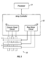
- FIG. 2 is a system block diagram illustrating one embodiment of an electronic device that may incorporate aspects of the invention.
- the electronic device includes a processor 21 which may be any general purpose single- or multi-chip microprocessor such as an ARM, Pentium®, Pentium II®, Pentium III®, Pentium IV®, Pentium® Pro, an 8051, a MIPS®, a Power PC®, an ALPHA®, or any special purpose microprocessor such as a digital signal processor, microcontroller, or a programmable gate array.
- the processor 21 may be configured to execute one or more software modules.
- the processor may be configured to execute one or more software applications, including a web browser, a telephone application, an email program, or any other software application.
- the processor 21 is also configured to communicate with an array controller 22.
- the array controller 22 includes a row driver circuit 24 and a column driver circuit 26 that provide signals to a display array or panel 30.
- the cross section of the array illustrated in Figure 1 is shown by the lines 1-1 in Figure 2.
- the row/column actuation protocol may take advantage of a hysteresis property of these devices illustrated in Figure 3. It may require, for example, a 10 volt potential difference to cause a movable layer to deform from the relaxed state to the actuated state. However, when the voltage is reduced from that value, the movable layer maintains its state as the voltage drops back below 10 volts.
- the movable layer does not relax completely until the voltage drops below 2 volts.
- the row/column actuation protocol can be designed such that during row strobing, pixels in the strobed row that are to be actuated are exposed to a voltage difference of about 10 volts, and pixels that are to be relaxed are exposed to a voltage difference of close to zero volts.
- each pixel sees a potential difference within the "stability window" of 3-7 volts in this example.
- This feature makes the pixel design illustrated in Figure 1 stable under the same applied voltage conditions in either an actuated or relaxed pre-existing state. Since each pixel of the interferometric modulator, whether in the actuated or relaxed state, is essentially a capacitor formed by the fixed and moving reflective layers, this stable state can be held at a voltage within the hysteresis window with almost no power dissipation. Essentially no current flows into the pixel if the applied potential is fixed.
- a display frame may be created by asserting the set of column electrodes in accordance with the desired set of actuated pixels in the first row.
- a row pulse is then applied to the row 1 electrode, actuating the pixels corresponding to the asserted column lines.
- the asserted set of column electrodes is then changed to correspond to the desired set of actuated pixels in the second row.
- a pulse is then applied to the row 2 electrode, actuating the appropriate pixels in row 2 in accordance with the asserted column electrodes.
- the row 1 pixels are unaffected by the row 2 pulse, and remain in the state they were set to during the row 1 pulse. This may be repeated for the entire series of rows in a sequential fashion to produce the frame.
- the frames are refreshed and/or updated with new display data by continually repeating this process at some desired number of frames per second.
- a wide variety of protocols for driving row and column electrodes of pixel arrays to produce display frames are also well known and may be used in conjunction with the present invention.
- Figures 4, 5A, and 5B illustrate one possible actuation protocol for creating a display frame on the 3x3 array of Figure 2.
- Figure 4 illustrates a possible set of column and row voltage levels that may be used for pixels exhibiting the hysteresis curves of Figure 3.
- actuating a pixel involves setting the appropriate column to -V bias , and the appropriate row to + ⁇ V, which may correspond to -5 volts and +5 volts respectively Relaxing the pixel is accomplished by setting the appropriate column to +V bias , and the appropriate row to the same + ⁇ V, producing a zero volt potential difference across the pixel. In those rows where the row voltage is held at zero volts, the pixels are stable in whatever state they were originally in, regardless of whether the column is at +V bias , or -V bias .
- actuating a pixel can involve setting the appropriate column to +V bias , and the appropriate row to - ⁇ V.
- releasing the pixel is accomplished by setting the appropriate column to -V bias , and the appropriate row to the same - ⁇ V, producing a zero volt potential difference across the pixel.
- Figure 5B is a timing diagram showing a series of row and column signals applied to the 3x3 array of Figure 2 which will result in the display arrangement illustrated in Figure 5A, where actuated pixels are non-reflective.
- the pixels Prior to writing the frame illustrated in Figure 5A, the pixels can be in any state, and in this example, all the rows are at 0 volts, and all the columns are at +5 volts. With these applied voltages, all pixels are stable in their existing actuated or relaxed states.
- pixels (1,1), (1,2), (2,2), (3,2) and (3,3) are actuated.
- columns 1 and 2 are set to-5 volts, and column 3 is set to +5 volts. This does not change the state of any pixels, because all the pixels remain in the 3-7 volt stability window.
- Row 1 is then strobed with a pulse that goes from 0, up to 5 volts, and back to zero. This actuates the (1,1) and (1,2) pixels and relaxes the (1,3) pixel. No other pixels in the array are affected.
- column 2 is set to -5 volts
- columns 1 and 3 are set to +5 volts.
- Row 3 is similarly set by setting columns 2 and 3 to -5 volts, and column 1 to +5 volts.
- the row 3 strobe sets the row 3 pixels as shown in Figure 5A. After writing the frame, the row potentials are zero, and the column potentials can remain at either +5 or -5 volts, and the display is then stable in the arrangement of Figure 5A. It will be appreciated that the same procedure can be employed for arrays of dozens or hundreds of rows and columns.
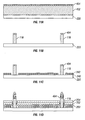
- FIGS 18A and 18B are system block diagrams illustrating an embodiment of a display device 40.
- the display device 40 can be, for example, a cellular or mobile telephone.
- the same components of display device 40 or slight variations thereof are also illustrative of various types of display devices such as televisions and portable media players.
- the display device 40 includes a housing 41, a display 30, an antenna 43, a speaker 44, an input device 48, and a microphone 46.
- the housing 41 is generally formed from any of a variety of manufacturing processes as are well known to those of skill in the art, including injection molding, and vacuum forming.
- the housing 41 may be made from any of a variety of materials, including but not limited to plastic, metal, glass, rubber, and ceramic, or a combination thereof.
- the housing 41 includes removable portions (not shown) that may be interchanged with other removable portions of different color, or containing different logos, pictures, or symbols.
- the display 30 of exemplary display device 40 may be any of a variety of displays, including a bi-stable display, as described herein.
- the display 30 includes a flat-panel display, such as plasma, EL, OLED, STN LCD, or TFT LCD as described above, or a non-flat-panel display, such as a CRT or other tube device, as is well known to those of skill in the art.
- the display 30 includes an interferometric modulator display, as described herein.
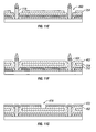
- the components of one embodiment of exemplary display device 40 are schematically illustrated in Figure 18B.
- the illustrated exemplary display device 40 includes a housing 41 and can include additional components at least partially enclosed therein.
- the exemplary display device 40 includes a network interface 27 that includes an antenna 43 which is coupled to a transceiver 47.
- the transceiver 47 is connected to a processor 21, which is connected to conditioning hardware 52.
- the conditioning hardware 52 may be configured to condition a signal (e.g. filter a signal).
- the conditioning hardware 52 is connected to a speaker 44 and a microphone 46.
- the processor 21 is also connected to an input device 48 and a driver controller 29.
- the driver controller 29 is coupled to a frame buffer 28, and to an array driver 22, which in turn is coupled to a display array 30.
- a power supply 50 provides power to all components as required by the particular exemplary display device 40 design.
- the network interface 27 includes the antenna 43 and the transceiver 47 so that the exemplary display device 40 can communicate with one ore more devices over a network. In one embodiment the network interface 27 may also have some processing capabilities to relieve requirements of the processor 21.
- the antenna 43 is any antenna known to those of skill in the art for transmitting and receiving signals. In one embodiment, the antenna transmits and receives RF signals according to the IEEE 802.11 standard, including IEEE 802.11(a), (b), or (g). In another embodiment, the antenna transmits and receives RF signals according to the BLUETOOTH standard. In the case of a cellular telephone, the antenna is designed to receive CDMA, GSM, AMPS or other known signals that are used to communicate within a wireless cell phone network.
- the transceiver 47 pre-processes the signals received from the antenna 43 so that they may be received by and further manipulated by the processor 21.
- the transceiver 47 also processes signals received from the processor 21 so that they may be transmitted from the exemplary display device 40 via the antenna 43.
- the transceiver 47 can be replaced by a receiver.
- network interface 27 can be replaced by an image source, which can store or generate image data to be sent to the processor 21.
- the image source can be a digital video disc (DVD) or a hard-disc drive that contains image data, or a software module that generates image data.
- Processor 21 generally controls the overall operation of the exemplary display device 40.
- the processor 21 receives data, such as compressed image data from the network interface 27 or an image source, and processes the data into raw image data or into a format that is readily processed into raw image data.
- the processor 21 then sends the processed data to the driver controller 29 or to frame buffer 28 for storage.
- Raw data typically refers to the information that identifies the image characteristics at each location within an image. For example, such image characteristics can include color, saturation, and gray-scale level.
- the processor 21 includes a microcontroller, CPU, or logic unit to control operation of the exemplary display device 40.
- Conditioning hardware 52 generally includes amplifiers and filters for transmitting signals to the speaker 44, and for receiving signals from the microphone 46. Conditioning hardware 52 may be discrete components within the exemplary display device 40, or may be incorporated within the processor 21 or other components.
- the driver controller 29 takes the raw image data generated by the processor 21 either directly from the processor 21 or from the frame buffer 28 and reformats the raw image data appropriately for high speed transmission to the array driver 22. Specifically, the driver controller 29 reformats the raw image data into a data flow having a raster-like format, such that it has a time order suitable for scanning across the display array 30. Then the driver controller 29 sends the formatted information to the array driver 22.
- a driver controller 29, such as a LCD controller is often associated with the system processor 21 as a stand-alone Integrated Circuit (IC), such controllers may be implemented in many ways. They may be embedded in the processor 21 as hardware, embedded in the processor 21 as software, or fully integrated in hardware with the array driver 22.
- IC Integrated Circuit
- the array driver 22 receives the formatted information from the driver controller 29 and reformats the video data into a parallel set of waveforms that are applied many times per second to the hundreds and sometimes thousands of leads coming from the display's x-y matrix of pixels.
- driver controller 29 is a conventional display controller or a bi-stable display controller (e.g., an interferometric modulator controller).
- array driver 22 is a conventional driver or a bi-stable display driver (e.g., an interferometric modulator display).
- a driver controller 29 is integrated with the array driver 22.
- display array 30 is a typical display array or a bi-stable display array (e.g., a display including an array of interferometric modulators).
- the input device 48 allows a user to control the operation of the exemplary display device 40.
- input device 48 includes a keypad, such as a QWERTY keyboard or a telephone keypad, a button, a switch, a touch-sensitive screen, a pressure- or heat-sensitive membrane.
- the microphone 46 is an input device for the exemplary display device 40. When the microphone 46 is used to input data to the device, voice commands may be provided by a user for controlling operations of the exemplary display device 40.
- Power supply 50 can include a variety of energy storage devices as are well known in the art.
- power supply 50 is a rechargeable battery, such as a nickel-cadmium battery or a lithium ion battery.
- power supply 50 is a renewable energy source, a capacitor, or a solar cell, including a plastic solar cell, and solar-cell paint.
- power supply 50 is configured to receive power from a wall outlet.
- control programmability resides, as described above, in a driver controller which can be located in several places in the electronic display system. In some cases control programmability resides in the array driver 22. Those of skill in the art will recognize that the above-described optimization may be implemented in any number of hardware and/or software components and in various configurations.
- Figures 6A-6C illustrate three different embodiments of the moving mirror structure.
- Figure 6A is a cross section of the embodiment of Figure 1, where a strip of metal material 14 is deposited on orthogonally extending supports 18.
- the moveable reflective material 14 is attached to supports at the corners only, on tethers 32.
- the moveable reflective material 14 is suspended from a deformable layer 34.
- This embodiment has benefits because the structural design and materials used for the reflective material 14 can be optimized with respect to the optical properties, and the structural design and materials used for the deformable layer 34 can be optimized with respect to desired mechanical properties.
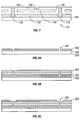
- Figure 7 is a cross-sectional illustration of an embodiment of an interferometric modulator element 112, which is similar in structure to the modulator element of Figure 6C.
- the modulator element 112 includes a fixed mirror layer within an optical stack 116 formed on a transparent substrate 120.
- the optical stack 116 may comprise two or more distinct layers.
- the optical stack 116 comprises an indium tin oxide (ITO) layer underneath a layer of chrome.
- the optical stack 116 may comprise an oxide layer located over the chrome layer.
- the optical stack 116 is alternately referred to herein as the electrode layer.
- posts 118 extend upward from the substrate 120 and support a flexible layer 134, alternately referred to herein as a deformable layer or a mechanical layer.
- the flexible layer 134 is electrically and physically connected to a movable mirror layer 114 via a conductive member 124.
- An interferometric cavity 119 is thus formed between the movable mirror 114 and the fixed mirror within the optical stack 116.
- the application of a voltage to both the movable mirror 114 and the fixed mirror will result in an electrostatic force between layers 114 and 116 causing the flexible layer 134 to deflect, so as to permit the movable mirror 114 to move closer to the optical stack 116.
- the movable mirror 114 can move closer or further from the optical stack 116, depending on the change in voltage. It is desirable that the posts 118 that support the flexible layer 134 be sufficiently stiff that the posts 118 not bend or deflect when the flexible layer 134 deflects.
- support posts such as post 118 of Figure 7 may not be located directly on substrate 120. Although not shown in Figure 7, the support posts 118 may instead be located on top of one or more of the layers which form the optical stack 116, or on top of a masking layer. As will be apparent from the following detailed description, the existence of layers underlying the support posts will depend in part on the particular methods and materials used to create the interferometric modulator.
- support post encompasses not only the variety of post structures depicted or described with respect to the various embodiments disclosed in the application, but also encompasses any structure suitable for providing support for the flexible layer 134, or similar components of an interferometric modulator element.
- these structures may comprise wall-like structures which are substantially longer in one dimension than they are wide in another.
- two intersecting wall structures may serve as a single support post, such that if the structures were to be viewed from above, they would form a cross.
- Such alternate structures which may provide necessary spacing between components supported by such structures, may advantageously also increase the functional area of the display.
- the term support post is used herein to refer to any of these support-providing structures.
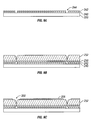
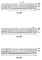
- Figures 8A-81 depict certain steps of one embodiment of a method of making one embodiment of an interferometric modulator element 112, such as depicted in Figure 7.
- Each of Figures 8A-8I is a side cross section view of the element 112 illustrating changes as additional layers are deposited, patterned, and etched in forming the interferometric modulator element 112.
- the substrate 120 of Figure 7, onto which the element 112 is formed includes a glass substrate 220.
- Each of the layers described herein may comprise any suitable material known in the art.
- an indium tin oxide (ITO) layer 240, and a chrome layer 242 can be deposited onto the glass substrate 220. These layers are subsequently patterned and etched to define addressing electrodes for individual modulator elements.
- ITO indium tin oxide
- chrome layer 242 can be deposited onto the glass substrate 220.
- posts will be formed in the apertures 244 between the electrodes.
- layers of oxide 250, sacrificial material 252, and mirror metal 254 are deposited over the layer 242.
- a mask layer 256 can be deposited, patterned, and etched to define a post region 258 in the mask layer 256.
- layers 254 and 252 are etched using the mask layer 256 of Figure 8C to form a hole or opening 260 extending through the layers 254 and 252 down to the oxide layer 250, after which the mask layer 256 is removed. While the profile of the opening 260 is depicted as v-shaped in the illustrated embodiment, it is to be recognized that the shape of the opening 260 may vary in other embodiments based on details of the photomasks used or on other details of the photolithography and etching processes used in an embodiment.
- a second sacrificial layer 262 is deposited onto exposed portions of the layers.
- the sacrificial layers 252 and 262 include molybdenum. As discussed above, the process in other embodiments may use any suitable material known in the art to accomplish the steps set forth above.
- a resist layer 272 is deposited on the exposed portions of the layers, patterned, and etched to define an aperture 274 in the resist layer 272.
- the aperture 274 corresponds to the location of the conductive member 108 that physically and electrically couples the movable mirror 114 to the deflectable membrane 134 of the interferometric modulator element 112 (See Figure 7).
- the sacrificial layer 262 is etched to define an opening corresponding to the conductive member 124.
- the resist layer is then removed, and a mechanical layer 282 is deposited on the exposed portions of the layers to form the conductive member 124 and the flexible layer 134 of Figure 7.
- a resist layer 292 is deposited on the mechanical layer 282 and masked to define other structures (not shown) of the mechanical layer.
- the sacrificial layers 252 and 262 are removed to define the optical cavity of the interferometric modulator element 112 and to separate the movable mirror 114 from the layers below it and, except for conductive member 124, from the layers above it as well.
- a xenon diflouride based process is used to remove the sacrificial layers.
- the post 118 in this embodiment is formed above another layer of material, rather than directly on the substrate as depicted in Figure 7.
- the post 118 is formed over a portion of the oxide layer 250, rather than directly on the substrate 220.
- the post 118 is thus formed by the mechanical layer 282 of Figure 8H.
- forming the post opening 260 (as shown in Figure 8D), as well as forming the mechanical layer 282 into the post opening (as shown in Figure 8G) requires precise process control that can limit the types of fabrication facility and fabrication equipment that can be used to fabricate the interferometric modulator element 112.
- Figures 9A-9E are cross-sectional views of certain steps of a method of making an alternate embodiment of an interferometric modulator in which a reflective surface is located on the underside of the flexible layer.
- a layer 240 of ITO is deposited on a substrate 220, and a layer 242 of chrome is deposited above the ITO layer 240.
- Layers 240 and 242 are then subsequently patterned and etched to define addressing electrodes for individual modulator elements.
- posts will be formed in the apertures 244 between the electrodes.
- layers 240 and 242 are etched so as to form addressing electrodes but leave material at the post locations, such that the posts will overlie this residual material.
- a layer 250 of oxide is deposited on top of the chrome layer 242, and a layer of sacrificial material 252 is deposited above the oxide layer 250.
- a mask layer 356 has been deposited and patterned to form apertures 358.
- sacrificial layer 252 is then etched, using the mask layer 356 as a guide, to form a hole or opening 360 in the sacrificial layer 252.
- the mask layer 356 is removed.
- a mechanical layer 382 is then deposited over the sacrificial layer, and along the edges of hole 360, forming both the deformable layer and the support post structure.
- this mechanical layer 382 may be madeof a reflective material, such that the layer 382 itself will serve as the movable reflective layer.
- a reflective layer (not shown) may be deposited on the sacrificial layer 252 prior to the deposition of mechanical layer 382, such that mechanical layer 382 is deposited on top of the reflective layer.
- the mechanical layer 382 may then be patterned and etched to form various features (not shown).
- a release etch is then performed to remove the layer 252 of sacrificial material, forming an interferometric cavity 319, as seen in Figure 9E.
- An interferometric modulator 312 is thus formed in which the underside of the deformable layer 382 serves as the movable reflective surface.
- Figures 10A-10G are cross-sectional views illustrating certain steps of another embodiment of a method of making one embodiment of the interferometric modulator element 112, such as depicted in Figure 7.
- the method includes the steps depicted in Figures 8A-8E.
- a resist layer 272 is deposited on the sacrificial layer 262 and patterned and etched to define apertures 274 and the post openings 260.
- the apertures 274 define the location of the conductive member 124
- the post openings 260 define the location of the posts 118.
- the sacrificial layers 252 and 262 are etched using the resist layer 272 as a mask to define an opening 276 for the conductive member 124 and openings 260 for the support post 118.
- a planararization layer 294 is deposited on exposed portions of the layers.
- the planarization layer 294 can be formed of organic or polymer materials, or any other suitable photo-patternable material such as are known in the art.
- the planarization layer 294 is formed of a photoresist material.
- the planarization layer 294 can be formed of spin-on materials, such as spin-on-glass.
- the planarization layer 294 is patterned and etched in the form of the post 118.
- the planarization layer 294 of Figure 10D is hardened to increase its rigidity, as more fully explained below.
- the hardened planarization material thus has increased strength and other improved physical properties as compared to the resist material from which it was originally formed. These improved properties enable the post 118 formed from the hardened material to provide improved support for a flexible layer, such as flexible layer 134 of Figure 7.
- the planarization material is a photoresist material
- the planarization material can be hardened using exposure to high temperatures to heavily cross link, and harden, the photoresist material.
- the mechanical layer 282 is desirably deposited over the posts 118 and the sacrificial layer 262.
- a resist layer 292 is deposited and masked to define other structures (not shown) of the mechanical layer 282.
- the sacrificial layers 252 and 262 are removed to define the optical cavity of the interferometric modulator element 112 and to separate the movable mirror 114 from the mechanical layer 134 located above the mirror and the optical stack 116 located below the mirror.
- the planarization material forms the post 118. While the planarization material will generally have sufficient hardness to function as a support post over the lifetime of an interferometric display, some slight shift in the color reflected by a particular modulator may occur over time, because the planarization material may never become fully hardened.
- support posts made from planarization materials may not be desirable.
- the hardening process typically undesirably exposes the other layers, e.g., the ITO layer, to high temperatures.
- the modulator elements structure is designed to support the flexible layer 134 in as close to a single plane as is possible.
- the position of the flexible layer 134 depends upon residual tensile stresses within the flexible layer, which pull the flexible layer toward a substantially flat position.
- the existence and magnitude of these residual tensile forces may be controlled, and depend on factors such as the materials and the parameters of the deposition process, such as the temperature at which the material is deposited and the rate of deposition.
- the effect of these residual tensile forces is illustrated in in Figure 10G, wherein the unattached portion of the flexible layer 10G is substantially flat.
- the post 118 must exert a restraining force on the flexible layer 134. Due to the thinness of the support post 118 in the region underlying the flexible layer 134 at the tip 119 of the support post, there is the potential for mechanical failure at the tip 119. This failure can take the form of partial delamination between the layer 134 and the upper surface of the support post 118, which may permit the layer 134 to move further away from the fixed mirror within the optical stack 116, thereby affecting the interferometric properties of the cavity.
- an increased range of movement could be the result of one or more fractures within the tip 119 of the support post 118, which would allow the flexible layer 134 to move further upward. If such a mechanical failure occurs, this slight mechanical failure may not occur until a point in time well into the useful lifetime of the interferometric modulator element, and may not result in an easily perceivable shift in the reflected wavelength of the modulator element.
- a flexible layer 134 which is slightly curved is suitable. However, this same curvature increases the fragility of the post lips, so over long periods of time, a partiallycurved mechanical layer may be undesirable.
- a process for forming the posts 118 desirably does not require high temperatures or other extreme conditions, while still providing the post 118 with sufficient rigidity to satisfy those embodiments of the modulator element 112 that require such additional rigidity.
- this process may advantageously utilize support posts having a substantially flat upper surface, and may also utilize a planarization layer to provide a substantially flat surface for deposition of a mechanical layer.
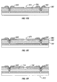
- Figures 11A-11K illustrate certain steps of one embodiment of a method of making one embodiment of an interferometric modulator element 112, such as depicted in Figure 7, including steps for forming a post prestructure on the substrate 120.
- the substrate 120 of Figure 7 includes the glass substrate 220 of Figure 11A.
- Figure 11 A depicts an early step in a method of forming an interferometric modulator element 112 wherein a spin on glass (SOG) layer 402 is deposited on a glass substrate 220 and a resist layer 404 is deposited on the SOG layer 402.
- the layer 402 may be formed using other deposition techniques such as by performing physical vapor deposition (PVD), chemical vapor deposition (CVD), plasma chemical vapor deposition (PVCD), or any other suitable process known in the art.
- a masking layer may be deposited on substrate 220, patterned, and etched prior to the deposition of the layer 402, which will form posts 118.
- this masking layer is patterned and etched such that once the interferometric modulator 112 is formed, the masking layer exists only under the support posts 118.
- the masking layer prevents light from entering the interferometric modulating element in a non-functional area. Subsequent undesired reflections of such stray light can negatively impact the image quality of an interferometric modulator-based display.
- preformed support posts such as posts 118 of Figure 11B may be formed of different materials, or in different positions, than the spin-on glass posts of Figure 11B.
- preformed posts comprising silicon oxide, another oxide material, or metal may be formed by depositing a layer of oxide via physical vapor deposition (PVD) on the transparent substrate, and then patterning and etching the layer of oxide to form support posts.
- PVD physical vapor deposition
- support posts, particularly those formed of a material which does not require annealing at temperatures as high as spin-on glass can be formed after certain other layers have been deposited.
- support posts made of oxide, metal, planarization material, or any other suitable material are formed after the ITO and chrome layers are deposited on the substrate.
- the placement of support posts above the electrode layer, particularly those support posts made from reflective material may advantageously reduce or eliminate the need for a masking layer to hide the reflective lower surface of the post from the viewer, as discussed above.
- the resist layer 404 is patterned and developed to yield a mask that allows an etch process to form the post structures 118 from SOG layer 402 of Figure 11A.
- the post structures 118 include at least two posts. Remaining portions of the resist layer form post masks 404 on top of the post structures.
- the mask layer 404 can be a lift-off resist, such as a lift-off resist material made by MicroChem Corp, of Newton, MA.
- the SOG layer 402 thus forms a post prestructure on the substrate 220.
- the ITO layer 240 and chrome layer 242 are deposited on the glass substrate 220, then patterned and etched to form portions of the optical stack 116 of Figure 7.
- the rigid glass layer 402 of Figure 10A is applied before the ITO 240 and chrome layer 242, allowing a rigid post 118 to be formed without needing to expose any other layers to high temperature processes that would typically tend to damage materials such as are in the ITO layer 240.
- the oxide layer 250, sacrificial layer 252, and mirror metal layer 254 are deposited onto exposed portions of the layers. Note that these layers can also be deposited onto the post mask 404.
- subsequent layers such as the oxide layer 250 are typically shadowed by the post 118. This shadowing causes the oxides 250 to taper off to the post. This taper is not so severe as to cause the oxide to fail to cover the underlying ITO 240 and chrome 242 layers and not so extensive as to extend beyond the minimum feature size gap that would normally exist between the post and the mirror. Thus the shadowing effect does not impact the optical performance or percent active area of the modulator.
- the mirror metal layer 254 is patterned and etched away from the posts 118 to define gaps 460 between the post 118 and the mirror layer 254.
- another sacrificial layer 462 is deposited on exposed portions of the layers.
- the sacrificial layers 252 and 462 are molybdenum.
- the post mask 404, and the residual layers that have been deposited on top of it, are removed using techniques such as those well known in the art.
- the lift-off resist removal technique is used.
- a planarization matieral which in this case is a resist layer 472, is deposited on exposed portions of the layers, patterned, and etched to define a cavity 474.
- the sacrificial layer 462 is etched to further define the cavity 474.
- the cavity 474 defines the form of the conductive connector 124 that extends between the flexible layer 134 and the mirror 114 (see Figure 7).
- etch-back planarization is performed to etch the resist layer 472 back to the sacrificial layer 462 so that the top of the post 118, the remaining resist 472 and the sacrificial layer 462 define a substantially planar surface.
- a mechanical layer 492 is deposited on this substantially planar surface. The mechanical layer 492 also fills the cavity 474 to form the conductive connector 124. At this point, pattern and etch steps are performed on the mechanical layer 492.
- the remaining resist layer 472 is removed, for example, by using an asher, e.g., a barrel etcher or a plasma etcher, to oxidize the resist layer 472 to form a cavity 476.
- an asher e.g., a barrel etcher or a plasma etcher
- the sacrificial layers are removed.
- xenon difluoride is used to remove the sacrificial layers 252 and 462.
- the movable mirror 114 and the deflectable membrane 134 are thus separated from the fixed members of the element 112.
- embodiments may include other processing steps.
- other features in the mechanical layer 492 can be formed during the pattern and etch of this layer.
- the post material may be deposited as a layer 402 which is then etched to form support posts 118, as seen in Figures 11A and 11B, greater control over the shape of the upper surface of the posts 118 is available than in the case where the posts are formed after other material has been deposited on the substrate.
- flexible layers which are substantially flat along the upper surface of the support posts can be formed, and the post can be made of more robust material than can be deposited later in the process.
- the flexible layer 134 is formed in, and tends to dwell in, a state in which the entire layer 134 is substantially flat, the residual tensile forces will not contribute to mechanical failure which permits movement of the flexible layer 134 father upward than is already permitted. Specifically, because the residual tensile forces are pulling in a direction parallel to the upper surface of the support posts 118 when the flexible layer 134 is in the unactuated state, there will be significantly less risk of delamination between the flexible layer 134 and the support post 118 8 than if the surface was oriented in a direction not parallel to the tensile force.
- Figures 12A-12E are cross-sectional views illustrating certain steps of another embodiment of a method of making one embodiment of the interferometric modulator element 112, such as depicted in Figure 7, including steps for forming a post prestructure on the substrate 120.
- This embodiment includes the steps depicted in Figures 11A-11E.
- the residual layers are stripped from the tops of the posts 118 and planarization material, which in this embodiment is a resist layer 502, is deposited in place of the second sacficifial layer 462 of Figure 11F.
- the resist layer 502 is patterned and etched to define the region 474 into which the conductor 124 can be formed.
- etch back planarization is performed on the resist layer 502 so that the resist layer and the post 118 define a substantially planar surface.
- the mechanical layer 492 is deposited as in the embodiment depicted in Figure 11I. The mechanical layer 492 is subsequently patterned and etched.
- an asher is used to oxidize away the resist layer 502 (shown in Figure 12C) to define the open region 476.
- the region 476 is larger than in the embodiment depicted in Figure 111 because the region 476 in this embodiment also includes the volume that was occupied by the sacrificial layer 462 in Figure 111.
- the sacrificial layer 252 of Figure 11D is removed to define the interferometric modulator element 112.
- the embodiment depicted in Figures 12A-12E desirably uses the photoresist layer 502, which is also used to pattern the aperture 474 for the conductor 124, as the second sacrificial layer 462 so as to reduce the total number of process steps as compared to the embodiment depicted in Figures 10A-10K.
- planarization material is used to provide the upper sacrificial layer, etch-back planarization can be performed, permitting the formation of a modulator element which, as discussed with respect to Figure 11K, is less susceptible to changes in its interferometric properties over time.
- preformed posts 118 can be used to support a combination mechanical/reflective layer, such as layer 382 of Figure 9G, creating an interferometric modulator similar to the modulator of Figure 6A.
- a method of fabricating such an embodiment includes steps of Figures 11A-11C. Following these steps, as illustrated in Figure 13A, an oxide layer 250 is deposited over the chrome layer 242, and a layer of sacrificial material 252 is deposited over the oxide layer 250.
- a mechanical layer 492 is then deposited over the substantially planar surface provided by the resist layer 512 and the support posts 118.
- this mechanical layer 492 may be made of a reflective material, such that the layer itself will serve as the movable reflective layer.
- a reflective layer (not shown) may be deposited on the resist layer 512 prior to the deposition of mechanical layer 492, such that mechanical layer 492 is deposited on top of the reflective layer.
- the mechanical layer 492 is then patterned and etched to form various features (not shown).
- an asher is used to oxidize away the resist layer 512 (shown in Figure 13D) to define an open region 476.
- a release etch is then performed to remove the layer 252 of sacrificial material, forming an interferometric cavity 519, as seen in Figure 13F.
- An interferometric modulator 512 in which the underside of the deformable layer 492 serves as the movable reflective surface is thus formed.
- any residual tensile forces within the deformable layer 492 will not tend to cause mechanical failures of the type discussed above, but will instead bias the deformable layer 492 to return to the position depicted in Figure 13F.
- a method for forming cap structures above posts includes the steps of Figure 11A-11I, wherein preformed support posts comprising a material such as spin-on glass are fabricated, a planarization layer is used to provide a substantially flat surface, and a mechanical layer is deposited over the substantially flat surface and etched to form various features (not depicted), as discussed above.
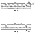
- a layer of insulating material 740 is deposited over the mechanical layer 492.
- a layer of rigid material 750 is then deposited over the insulating layer 740.
- the layer of rigid material may not be necessary, if the layer of insulating material 740 is sufficiently thick and/or rigid.
- the layer of insulating material 740 may comprise, in one embodiment, an oxide such as silicon oxide, but any suitable material which can serve as an electrical insulator may be used.
- the layer of rigid material 750 may be any suitable material, and the use of an insulating layer 740 in contact with the patterned mechanical layer 492 enables the use of electrically conductive material in the rigid layer 750, as the rigid layer is electrically isolated from the mechanical layer.
- the rigid layer 750 comprises the same material used in the mechanical layer 492.
- both the mechanical layer 492 and the rigid layer 750 comprise nickel.
- one or both of the layers 492 and 750 may comprise aluminum.
- a wide range of materials may be suitable for use in the rigid layer 750, as depositing a sufficiently thick layer of these materials may provide the necessary rigidity.
- the resist layer 472 is removed, such as by using an asher, as discussed previously, leaving cavities 474.
- a release etch is performed to remove the sacrificial layers 462 and 452, separating the mirror layer 114 from the flexible layer 134 above the mirror and the optical stack 116 below the mirror, thereby forming a modulator element 712. If the mechanical layer 492 (see Figure 14C) was previously etched so as to totally remove the mechanical layer from above the posts 118, a mechanical layer 492 (see Figure 14C) forms a flexible layer 134 wherein the flexible layer is suspended from the insulated underside of the caps 760.
- the caps 760 extend at least partially over the mirrors 114, the surface area required for electrical isolation does not negatively impact the amount of functional area in the modulator element 712.
- the caps 760 may be formed solely of insulating material 740, if the insulating material has sufficient thickness or rigidity to support the flexible layer 134.
- the preformed support posts may comprise a column of conductive material such that the top of the post 118 may be placed in electrical communication with an element located below the post.
- the insulating layer 740 may be etched over the support post so as to expose the conductive material within the post 118 without exposing the patterened mechanical layer 492.
- the layer of rigid material 750 is deposited over the insulating layer 740, the cavity in the insulating layer is filled, and provided the rigid material 750 is electrically conductive, an electrical connection can be made between the top of the resulting cap 760 and an element underlying the post 118.
- Overlying support material may be formed above the other types of support posts discussed in this application.
- a method of providing an overlying cap structure includes the steps depicted in Figures 10A-10F.
- a layer of insulating material 740 is deposited over the patterned mechanical layer 282, and a layer of rigid support material 750 is then deposited over the insulating layer 740, as can be seen in Figure 15A.
- cap structures 760 have been created by etching the rigid support layer 750, using the insulating layer 740 as an etch stop.
- the insulating layer 740 has then been etched, using the underlying mechanical layer 282 and sacrificial layer 262 as etch stops.
- an interferometric modulator element 712 is formed, by etching the sacrificial material 252 and 262 to release the mirror 114, as discussed above.
- the interferometric modulator element 712 comprises posts 188 made from planarization material, and an overlying cap 760, which provides additional support for the flexible layer 134.
- the mechanical layer 282 may be etched so as to completely remove the mechanical layer overlying the curved upper surface of the posts 188.
- the caps 760 can then extend sufficiently beyond the edges of the post 188 to support the flexible layer 134.
- FIG. 8A-8H Another method of providing additional support for support posts, such as the support posts 118 of Figure 81, includes the steps of Figures 8A-8H.
- an insulating layer 740 and a support layer 750 are deposited above the patterened mechanical layer 282, as seen in Figure 16A.
- the rigid support layer 750 is first etched, followed by the insulator layer 740, forming a cap structure 760 of additional support material.
- an interferometric modulator 712 is formed by performing a release etch, removing the sacrificial layers 262 and 252, releasing the mirror 114, as discussed above.
- FIG. 17F Another method of forming cap structures includes forming an interferometric modulator comprising freestanding support posts 652 (see Figure 17F).
- This method includes the process of Figures 8A-8E.
- a resist layer 640 is deposited over the sacrificial layer 262.
- the resist mask 640 of Figure 17A need not have an aperture 274 for etching. Rather, the resist mask 640 need only provide apertures within the post holes 260, for etching the portion of sacrificial layer 262 exposed by the resist mask 640.
- FIG 17B it can be seen that the resist mask has been used to etch the sacrificial layer 262 to expose the oxide layer 250 underneath the post hole 260 of Figure 17A.
- a layer of support post material 650 is then deposited.
- the support post material is non-planarizing, and thus the deposited layer conforms to the shape of the underlying layers, leaving part of the post hole 260 unfilled, rather than filling the entirety of the post hole.
- the layer of support post material 650 may comprise material suitable for use as a mechanical layer, it will be understood that the selection of support post material need not be so limited. Rather, the support post material 650 may advantageously be a material which has significant rigidity, rather than the flexibility desirable in mechanical layer material. Additionally, the support post material 650 is desirably selectively etchable relative to the sacrificial layer 262.
- support post material 650 has been patterned and etched such that certain support post material beyond the vicinity of the post holes 260 (see Figure 17A) has been removed, leaving support posts 652.
- these support posts are roughly symmetrical about a central axis, and are thus substantially conical in shape in the center, having a wide, substantially flat outer edge area.
- the support posts may be wider in one direction than in another, and are thus substantially wedge-shaped.
- a layer of insulating material 840 is deposited over the support posts 652 and the exposed underlying sacrificial layer 262.
- the insulating material 840 is then patterned and etched so as to remove certain insulating material 840 overlying the sacrificial material 262, leaving insulating material only in the area around the support posts 652.
- An aperture 874 is then etched in the sacrificial layer, exposing the underlying mirror layer 254.
- a mechanical layer 860 is then deposited, such that it overlies the insulating material 840 and fills the aperture 874.
- the mechanical layer 860 is then patterned and etched to form features (not shown).
- FIG 17F it can be seen that a release etch has been performed to remove the sacrificial material 262 and 252, separating the mirror 114 from the surrounding material, as discussed above.
- An interferometric modulator element 812 is thus formed, having cap structures formed from insulating material 840, which are located above posts 652 and provide support for the flexible layer 134. In the depicted embodiment, no additional rigid support layer may be necessary, as the wide underlying support post 652 may provide sufficient rigidity.
- the order of layers and the materials forming these layers in the above embodiments are merely exemplary.
- the planarization layer can serve as the entire sacrificial material, which will then be removed to form the cavity between the deformable upper layer and the optical stack.
- other layers not shown, may be deposited and processed to form portions of the interferometric modulator element 112 or to form other structures on the substrate.
- these layers may be formed using alternative deposition materials, may be deposited in different order, or composed of different materials, as would be known to one of skill in the art, or as also discussed in more detail in the patents and applications discussed above.
- cap structures discussed above may be utilized in embodiments in which the flexible layer serves as the movable reflective layer.
- the embodiment depicted in Figure 13F may be modified to include cap structures at the top of the support posts, from which the flexible reflective layer is suspended.
- Other embodiments having a combination movable/reflective layer may be similarly modified to provide additional support, improved mechanical characteristics, and increased functional area within the display.
Abstract
Description
- The field of the invention relates to microelectromechanical systems (MEMS).
- Microelectromechanical systems (MEMS) include micro mechanical elements, actuators, and electronics. Micromechanical elements may be created using deposition, etching, and or other micromachining processes that etch away parts of substrates and/or deposited material layers or that add layers to form electrical and electromechanical devices. One type of MEMS device is called an interferometric modulator. As used herein, the term interferometric modulator or interferometric light modulator refers to a device that selectively absorbs and/or reflects light using the principles of optical interference. In certain embodiments, an interferometric modulator may comprise a pair of conductive plates, one or both of which may be transparent and/or reflective in whole or part and capable of relative motion upon application of an appropriate electrical signal. In a particular embodiment, one plate may comprise a stationary layer deposited on a substrate and the other plate may comprise a metallic membrane separated from the stationary layer by an air gap. As described herein in more detail, the position of one plate in relation to another can change the optical interference of light incident on the interferometric modulator. Such devices have a wide range of applications, and it would be beneficial in the art to utilize and/or modify the characteristics of these types of devices so that their features can be exploited in improving existing products and creating new products that have not yet been developed.
- In one embodiment, a method of forming an interferometric display element is provided, including providing a substrate, depositing a layer of support post material over the substrate, patterning the layer of support post material to form at least two support posts, forming an electrode layer over the substrate, where the forming of the electrode layer is done after the forming of the at least two support posts, forming at least a first sacrificial layer over the electrode layer, and forming a mechanical layer over the sacrificial layer, where the mechanical layer covers a portion of each of the at least two support posts.
- In another embodiment, an apparatus including a plurality of interferometric modulator elements is provided, where the interferometric modulator elements include an electrode layer located over the substrate, at least two support posts located on the substrate, and a mechanical layer located over the electrode layer, where the mechanical layer is supported by at least two support posts.
- In another embodiment, a method of making an interferometric display element is provided, including providing a substrate, forming support posts over the substrate, forming an electrode layer over the substrate, depositing a sacrificial layer over the electrode layer forming a substantially planar surface over the sacrificial layer, forming a mechanical layer over the substantially planar surface, forming an insulator layer over at least part of the mechanical layer; and forming a substantially rigid support layer over the insulation layer.
- In another embodiment, an apparatus is provided, including a transparent substrate, an electrode layer located over the substrate, a plurality of support posts located over the substrate, a rigid cap member located over each of at least some of the plurality of support posts, where the rigid cap member includes an insulator layer, and a mechanical layer located over the partially reflective electrode layer, where said mechanical layer is attached to the insulator layers of at least two rigid cap members.
- In another embodiment, an apparatus including means for conveying light is provided. The apparatus further comprises means for conducting electricity located over said conveying means, means for modifying an interferometric modulator cavity size, and means located on said conveying means for supporting said modifying means, wherein said supporting means comprise material with lower annealing temperature than said conducting means.
- In another embodiment, an apparatus including means for conveying light is provided. The apparatus further comprises means for conducting electricity located over said conveying means, means for modifying an interferometric modulator cavity size, means for supporting said modifying means, said supporting means located over said conveying means, and means for providing rigidity for said modifying means, said providing means located over at least some said supporting means and said providing means comprising an insulator layer, wherein the insulator layer is attached to said modifying layer.
-
- Figure 1 is an isometric view depicting a portion of one embodiment of an interferometric modulator display in which a movable reflective layer of a first interferometric modulator is in a released position and a movable reflective layer of a second interferometric modulator is in an actuated position.
- Figure 2 is a system block diagram illustrating one embodiment of an electronic device incorporating a 3x3 interferometric modulator display.
- Figure 3 is a diagram of movable mirror position versus applied voltage for one exemplary embodiment of an interferometric modulator of Figure 1.
- Figure 4 is an illustration of a set of row and column voltages that may be used to drive an interferometric modulator display.
- Figure 5A illustrates one exemplary frame of display data in the 3x3 interferometric modulator display of Figure 2.
- Figure 5B illustrates one exemplary timing diagram for row and column signals that may be used to write the frame of Figure 5A.
- Figure 6A is a cross section of the device of Figure 1.
- Figure 6B is a cross section of an alternative embodiment of an interferometric modulator.
- Figure 6C is a cross section of another alternative embodiment of an interferometric modulator.
- Figure 7 is a cross section of an embodiment of an interferometric modulator element, similar to the interferometric modulator of Figure 6C.
- Figures 8A-8I are cross sectional views illustrating certain steps of one embodiment of a method of making one embodiment of an interferometric modulator element, such as depicted in Figure 7.
- Figures 9A-9E are cross-sectional views illustrating certain steps of one embodiment of a method of making one embodiment of an interferometric modulator element in which the deformable layer serves as the movable mirror.
- Figures 10A-10G are cross sectional views illustrating certain steps of another embodiment of a method of making one embodiment of an interferometric modulator element, such as depicted in Figure 7.
- Figures 11 A-II K are cross sectional views illustrating certain steps of one embodiment of a method of making one embodiment of an interferometric modulator element, such as depicted in Figure 7, including steps for forming a post prestructure on a substrate.
- Figures 12A-12E are cross sectional views illustrating certain steps of another embodiment of a method of making one embodiment of an interferometric modulator element, such as depicted in Figure 7, including steps for forming a post prestructure on a substrate.
- Figures 13A-13F are cross-sectional views illustrating certain steps of one embodiment of a method of making another embodiment of an interferometric modulator element in which the deformable layer serves as the movable mirror, such as depicted in Figure 6A.
- Figures 14A-14D are cross sectional views illustrating certain steps of an embodiment of a method of making one embodiment of an interferometric modulator element, in which cap structures are located at the tops of the support posts.
- Figures 15A-15C are cross sectional views illustrating certain steps of another embodiment of a method of making one embodiment of an interferometric modulator element, in which cap structures are located at the tops of the support posts.
- Figures 16A-16C are cross sectional views illustrating certain steps of another embodiment of a method of making one embodiment of an interferometric modulator element, in which cap structures are located at the tops of the support posts.
- Figures 17A-17F are cross sectional views illustrating certain steps of another embodiment of a method of making one embodiment of an interterometric modulator element, in which cap structures are located at the tops of the support posts.
- Figures 18A-18B are system block diagrams illustrating an embodiment of a display device.
- An embodiment of the invention, as discussed in greater detail below, is an interferometric modulator element which includes an upper mechanical layer supported by at least two support posts. In one embodiment, these support posts are formed on a substrate before other layers are deposited on the substrate. Such a method advantageously permits the use of spin-on glass support posts, and other materials which must be annealed at a temperature high enough to damage other components of the interferometric modulator if those components were deposited before the annealing of the post.
- In other embodiments, support posts made from materials with lower annealing temperatures may be formed after the deposition of certain layers of materials having higher annealing temperatures, permitting the creation of support posts over these layers. Such an embodiment advantageously minimizes or eliminates the need for a masking layer between the posts and the viewer, as the layers on which the support posts rest may prevent the support posts from reflecting light back to the viewer.
- Another embodiment of the invention, as discussed in greater detail below, is a method of making an interferometric modulator element which includes a rigid cap portion atop at least two support posts. The method may also include providing a substantially planar surface on which the mechanical layer can be formed. The use of a cap portion advantageously provides additional rigidity to the support posts. In addition, the use of a rigid cap portion advantageously permits the use of thin support posts, providing the necessary surface area to support and electrically isolate adjacent mechanical layers. The use of a substantially flat mechanical layer advantageously prevents problems such as delamination between the support post and the mechanical layer, or damage to the edge of the support post, which might otherwise occur over time as a result of the residual tensile stresses in a non-flat mechanical layer. Thus, this invention provides a modulator having improved greater color accuracy over a longer period of time.
- The following detailed description is directed to certain specific embodiments of the invention. However, the invention can be embodied in a multitude of different ways. In this description, reference is made to the drawings wherein like parts are designated with like numerals throughout. As will be apparent from the following description, the embodiments may be implemented in any device that is configured to display an image, whether in motion (e.g., video) or stationary (e.g., still image), and whether textual or pictorial. More particularly, it is contemplated that the embodiments may be implemented in or associated with a variety of electronic devices such as, but not limited to, mobile telephones, wireless devices, personal data assistants (PDAs), hand-held or portable computers, GPS receivers/navigators, cameras, MP3 players, camcorders, game consoles, wrist watches, clocks, calculators, television monitors, flat panel displays, computer monitors, auto displays (e.g., odometer display, etc.), cockpit controls and/or displays, display of camera views (e.g., display of a rear view camera in a vehicle), electronic photographs, electronic billboards or signs, projectors, architectural structures, packaging, and aesthetic structures (e.g., display of images on a piece of jewelry). MEMS devices of similar structure to those described herein can also be used in non-display applications such as in electronic switching devices.
- One interferometric modulator display embodiment comprising an interferometric MEMS display element is illustrated in Figure 1. In these devices, the pixels are in either a bright or dark state. In the bright ("on" or "open") state, the display element reflects a large portion of incident visible light to a user. When in the dark ("off" or "closed") state, the display element reflects little incident visible light to the user. Depending on the embodiment, the light reflectance properties of the "on" and "off" states may be reversed. MEMS pixels can be configured to reflect predominantly at selected colors, allowing for a color display in addition to black and white.
- Figure 1 is an isometric view depicting two adjacent pixels in a series of pixels of a visual display, wherein each pixel comprises a MEMS interferometric modulator. In some embodiments, an interferometric modulator display comprises a row/column array of these interferometric modulators. Each interferometric modulator includes a pair of reflective layers positioned at a variable and controllable distance from each other to form a resonant optical cavity with at least one variable dimension. In one embodiment, one of the reflective layers may be moved between two positions. In the first position, referred to herein as the relaxed, the movable layer is positioned at a relatively large distance from a fixed partially reflective layer. In the second position, the movable layer is positioned more closely adjacent to the partially reflective layer. Incident light that reflects from the two layers interferes constructively or destructively depending on the position of the movable reflective layer, producing either an overall reflective or non-reflective state for each pixel.
- The depicted portion of the pixel array in Figure 1 includes two adjacent
interferometric modulators interferometric modulator 12a on the left, a movable and highly reflective layer 14a is illustrated in a relaxed position at a predetermined distance from a fixed partially reflective layer 16a. In theinterferometric modulator 12b on the right, the movable highlyreflective layer 14b is illustrated in an actuated position adjacent to the fixed partiallyreflective layer 16b. - The
fixed layers 16a, 16b are electrically conductive, partially transparent and partially reflective, and may be fabricated, for example, by depositing one or more layers each of chromium and indium-tin-oxide onto atransparent substrate 20. The layers are patterned into parallel strips, and may form row electrodes in a display device as described further below. Themovable layers 14a, 14b may be formed as a series of parallel strips of a deposited metal layer or layers (orthogonal to therow electrodes 16a, 16b) deposited on top ofposts 18 and an intervening sacrificial material deposited between theposts 18. When the sacrificial material is etched away, thedeformable metal layers 14a, 14b are separated from the fixed metal layers by a definedgap 19. A highly conductive and reflective material such as aluminum may be used for the deformable layers, and these strips may form column electrodes in a display device. - With no applied voltage, the
cavity 19 remains between the layers 14a, 16a and the deformable layer is in a mechanically relaxed state as illustrated by thepixel 12a in Figure 1. However, when a potential difference is applied to a selected row and column, the capacitor formed at the intersection of the row and column electrodes at the corresponding pixel becomes charged, and electrostatic forces pull the electrodes together. If the voltage is high enough, the movable layer is deformed and is forced against the fixed layer (a dielectric material which is not illustrated in this Figure may be deposited on the fixed layer to prevent shorting and control the separation distance) as illustrated by thepixel 12b on the right in Figure 1. The behavior is the same regardless of the polarity of the applied potential difference. In this way, row/column actuation that can control the reflective vs. non-reflective pixel states is analogous in many ways to that used in conventional LCD and other display technologies. - Figures 2 through 5B illustrate one exemplary process and system for using an array of interferometric modulators in a display application.
- Figure 2 is a system block diagram illustrating one embodiment of an electronic device that may incorporate aspects of the invention. In the exemplary embodiment, the electronic device includes a
processor 21 which may be any general purpose single- or multi-chip microprocessor such as an ARM, Pentium®, Pentium II®, Pentium III®, Pentium IV®, Pentium® Pro, an 8051, a MIPS®, a Power PC®, an ALPHA®, or any special purpose microprocessor such as a digital signal processor, microcontroller, or a programmable gate array. As is conventional in the art, theprocessor 21 may be configured to execute one or more software modules. In addition to executing an operating system, the processor may be configured to execute one or more software applications, including a web browser, a telephone application, an email program, or any other software application. - In one embodiment, the
processor 21 is also configured to communicate with anarray controller 22. In one embodiment, thearray controller 22 includes arow driver circuit 24 and acolumn driver circuit 26 that provide signals to a display array orpanel 30. The cross section of the array illustrated in Figure 1 is shown by the lines 1-1 in Figure 2. For MEMS interferometric modulators, the row/column actuation protocol may take advantage of a hysteresis property of these devices illustrated in Figure 3. It may require, for example, a 10 volt potential difference to cause a movable layer to deform from the relaxed state to the actuated state. However, when the voltage is reduced from that value, the movable layer maintains its state as the voltage drops back below 10 volts. In the exemplary embodiment of Figure 3, the movable layer does not relax completely until the voltage drops below 2 volts. There is thus a range of voltage, about 3 to 7 V in the example illustrated in Figure 3, where there exists a window of applied voltage within which the device is stable in either the relaxed or actuated state. This is referred to herein as the "hysteresis window" or "stability window." For a display array having the hysteresis characteristics of Figure 3, the row/column actuation protocol can be designed such that during row strobing, pixels in the strobed row that are to be actuated are exposed to a voltage difference of about 10 volts, and pixels that are to be relaxed are exposed to a voltage difference of close to zero volts. After the strobe, the pixels are exposed to a steady state voltage difference ofabout 5 volts such that they remain in whatever state the row strobe put them in. After being written, each pixel sees a potential difference within the "stability window" of 3-7 volts in this example. This feature makes the pixel design illustrated in Figure 1 stable under the same applied voltage conditions in either an actuated or relaxed pre-existing state. Since each pixel of the interferometric modulator, whether in the actuated or relaxed state, is essentially a capacitor formed by the fixed and moving reflective layers, this stable state can be held at a voltage within the hysteresis window with almost no power dissipation. Essentially no current flows into the pixel if the applied potential is fixed. - In typical applications, a display frame may be created by asserting the set of column electrodes in accordance with the desired set of actuated pixels in the first row. A row pulse is then applied to the
row 1 electrode, actuating the pixels corresponding to the asserted column lines. The asserted set of column electrodes is then changed to correspond to the desired set of actuated pixels in the second row. A pulse is then applied to therow 2 electrode, actuating the appropriate pixels inrow 2 in accordance with the asserted column electrodes. Therow 1 pixels are unaffected by therow 2 pulse, and remain in the state they were set to during therow 1 pulse. This may be repeated for the entire series of rows in a sequential fashion to produce the frame. Generally, the frames are refreshed and/or updated with new display data by continually repeating this process at some desired number of frames per second. A wide variety of protocols for driving row and column electrodes of pixel arrays to produce display frames are also well known and may be used in conjunction with the present invention. Figures 4, 5A, and 5B illustrate one possible actuation protocol for creating a display frame on the 3x3 array of Figure 2. Figure 4 illustrates a possible set of column and row voltage levels that may be used for pixels exhibiting the hysteresis curves of Figure 3. In the Figure 4 embodiment, actuating a pixel involves setting the appropriate column to -Vbias, and the appropriate row to +ΔV, which may correspond to -5 volts and +5 volts respectively Relaxing the pixel is accomplished by setting the appropriate column to +Vbias, and the appropriate row to the same +ΔV, producing a zero volt potential difference across the pixel. In those rows where the row voltage is held at zero volts, the pixels are stable in whatever state they were originally in, regardless of whether the column is at +Vbias, or -Vbias. As is also illustrated in Figure 4, it will be appreciated that voltages of opposite polarity than those described above can be used, e.g., actuating a pixel can involve setting the appropriate column to +Vbias, and the appropriate row to -ΔV. In this embodiment, releasing the pixel is accomplished by setting the appropriate column to -Vbias, and the appropriate row to the same -ΔV, producing a zero volt potential difference across the pixel. - Figure 5B is a timing diagram showing a series of row and column signals applied to the 3x3 array of Figure 2 which will result in the display arrangement illustrated in Figure 5A, where actuated pixels are non-reflective. Prior to writing the frame illustrated in Figure 5A, the pixels can be in any state, and in this example, all the rows are at 0 volts, and all the columns are at +5 volts. With these applied voltages, all pixels are stable in their existing actuated or relaxed states.
- In the Figure 5A frame, pixels (1,1), (1,2), (2,2), (3,2) and (3,3) are actuated. To accomplish this, during a "line time" for
row 1,columns column 3 is set to +5 volts. This does not change the state of any pixels, because all the pixels remain in the 3-7 volt stability window.Row 1 is then strobed with a pulse that goes from 0, up to 5 volts, and back to zero. This actuates the (1,1) and (1,2) pixels and relaxes the (1,3) pixel. No other pixels in the array are affected. To setrow 2 as desired,column 2 is set to -5 volts, andcolumns Row 3 is similarly set by settingcolumns column 1 to +5 volts. Therow 3 strobe sets therow 3 pixels as shown in Figure 5A. After writing the frame, the row potentials are zero, and the column potentials can remain at either +5 or -5 volts, and the display is then stable in the arrangement of Figure 5A. It will be appreciated that the same procedure can be employed for arrays of dozens or hundreds of rows and columns. It will also be appreciated that the timing, sequence, and levels of voltages used to perform row and column actuation can be varied widely within the general principles outlined above, and the above example is exemplary only, and any actuation voltage method can be used with the systems and methods described herein. - Figures 18A and 18B are system block diagrams illustrating an embodiment of a
display device 40. Thedisplay device 40 can be, for example, a cellular or mobile telephone. However, the same components ofdisplay device 40 or slight variations thereof are also illustrative of various types of display devices such as televisions and portable media players. - The
display device 40 includes ahousing 41, adisplay 30, anantenna 43, aspeaker 44, aninput device 48, and amicrophone 46. Thehousing 41 is generally formed from any of a variety of manufacturing processes as are well known to those of skill in the art, including injection molding, and vacuum forming. In addition, thehousing 41 may be made from any of a variety of materials, including but not limited to plastic, metal, glass, rubber, and ceramic, or a combination thereof. In one embodiment thehousing 41 includes removable portions (not shown) that may be interchanged with other removable portions of different color, or containing different logos, pictures, or symbols. - The
display 30 ofexemplary display device 40 may be any of a variety of displays, including a bi-stable display, as described herein. In other embodiments, thedisplay 30 includes a flat-panel display, such as plasma, EL, OLED, STN LCD, or TFT LCD as described above, or a non-flat-panel display, such as a CRT or other tube device, as is well known to those of skill in the art. However, for purposes of describing the present embodiment, thedisplay 30 includes an interferometric modulator display, as described herein. - The components of one embodiment of
exemplary display device 40 are schematically illustrated in Figure 18B. The illustratedexemplary display device 40 includes ahousing 41 and can include additional components at least partially enclosed therein. For example, in one embodiment, theexemplary display device 40 includes anetwork interface 27 that includes anantenna 43 which is coupled to atransceiver 47. Thetransceiver 47 is connected to aprocessor 21, which is connected toconditioning hardware 52. [Theconditioning hardware 52 may be configured to condition a signal (e.g. filter a signal).] Theconditioning hardware 52 is connected to aspeaker 44 and amicrophone 46. Theprocessor 21 is also connected to aninput device 48 and adriver controller 29. Thedriver controller 29 is coupled to aframe buffer 28, and to anarray driver 22, which in turn is coupled to adisplay array 30. Apower supply 50 provides power to all components as required by the particularexemplary display device 40 design. - The
network interface 27 includes theantenna 43 and thetransceiver 47 so that theexemplary display device 40 can communicate with one ore more devices over a network. In one embodiment thenetwork interface 27 may also have some processing capabilities to relieve requirements of theprocessor 21. Theantenna 43 is any antenna known to those of skill in the art for transmitting and receiving signals. In one embodiment, the antenna transmits and receives RF signals according to the IEEE 802.11 standard, including IEEE 802.11(a), (b), or (g). In another embodiment, the antenna transmits and receives RF signals according to the BLUETOOTH standard. In the case of a cellular telephone, the antenna is designed to receive CDMA, GSM, AMPS or other known signals that are used to communicate within a wireless cell phone network. Thetransceiver 47 pre-processes the signals received from theantenna 43 so that they may be received by and further manipulated by theprocessor 21. Thetransceiver 47 also processes signals received from theprocessor 21 so that they may be transmitted from theexemplary display device 40 via theantenna 43. - In an alternative embodiment, the
transceiver 47 can be replaced by a receiver. In yet another alternative embodiment,network interface 27 can be replaced by an image source, which can store or generate image data to be sent to theprocessor 21. For example, the image source can be a digital video disc (DVD) or a hard-disc drive that contains image data, or a software module that generates image data. -
Processor 21 generally controls the overall operation of theexemplary display device 40. Theprocessor 21 receives data, such as compressed image data from thenetwork interface 27 or an image source, and processes the data into raw image data or into a format that is readily processed into raw image data. Theprocessor 21 then sends the processed data to thedriver controller 29 or to framebuffer 28 for storage. Raw data typically refers to the information that identifies the image characteristics at each location within an image. For example, such image characteristics can include color, saturation, and gray-scale level. - In one embodiment, the
processor 21 includes a microcontroller, CPU, or logic unit to control operation of theexemplary display device 40.Conditioning hardware 52 generally includes amplifiers and filters for transmitting signals to thespeaker 44, and for receiving signals from themicrophone 46.Conditioning hardware 52 may be discrete components within theexemplary display device 40, or may be incorporated within theprocessor 21 or other components. - The
driver controller 29 takes the raw image data generated by theprocessor 21 either directly from theprocessor 21 or from theframe buffer 28 and reformats the raw image data appropriately for high speed transmission to thearray driver 22. Specifically, thedriver controller 29 reformats the raw image data into a data flow having a raster-like format, such that it has a time order suitable for scanning across thedisplay array 30. Then thedriver controller 29 sends the formatted information to thearray driver 22. Although adriver controller 29, such as a LCD controller, is often associated with thesystem processor 21 as a stand-alone Integrated Circuit (IC), such controllers may be implemented in many ways. They may be embedded in theprocessor 21 as hardware, embedded in theprocessor 21 as software, or fully integrated in hardware with thearray driver 22. - Typically, the
array driver 22 receives the formatted information from thedriver controller 29 and reformats the video data into a parallel set of waveforms that are applied many times per second to the hundreds and sometimes thousands of leads coming from the display's x-y matrix of pixels. - In one embodiment, the
driver controller 29,array driver 22, anddisplay array 30 are appropriate for any of the types of displays described herein. For example, in one embodiment,driver controller 29 is a conventional display controller or a bi-stable display controller (e.g., an interferometric modulator controller). In another embodiment,array driver 22 is a conventional driver or a bi-stable display driver (e.g., an interferometric modulator display). In one embodiment, adriver controller 29 is integrated with thearray driver 22. Such an embodiment is common in highly integrated systems such as cellular phones, watches, and other small area displays. In yet another embodiment,display array 30 is a typical display array or a bi-stable display array (e.g., a display including an array of interferometric modulators). - The
input device 48 allows a user to control the operation of theexemplary display device 40. In one embodiment,input device 48 includes a keypad, such as a QWERTY keyboard or a telephone keypad, a button, a switch, a touch-sensitive screen, a pressure- or heat-sensitive membrane. In one embodiment, themicrophone 46 is an input device for theexemplary display device 40. When themicrophone 46 is used to input data to the device, voice commands may be provided by a user for controlling operations of theexemplary display device 40. -
Power supply 50 can include a variety of energy storage devices as are well known in the art. For example, in one embodiment,power supply 50 is a rechargeable battery, such as a nickel-cadmium battery or a lithium ion battery. In another embodiment,power supply 50 is a renewable energy source, a capacitor, or a solar cell, including a plastic solar cell, and solar-cell paint. In another embodiment,power supply 50 is configured to receive power from a wall outlet. - In some implementations control programmability resides, as described above, in a driver controller which can be located in several places in the electronic display system. In some cases control programmability resides in the
array driver 22. Those of skill in the art will recognize that the above-described optimization may be implemented in any number of hardware and/or software components and in various configurations. - The details of the structure of interferometric modulators that operate in accordance with the principles set forth above may vary widely. For example, Figures 6A-6C illustrate three different embodiments of the moving mirror structure. Figure 6A is a cross section of the embodiment of Figure 1, where a strip of
metal material 14 is deposited on orthogonally extending supports 18. In Figure 6B, the moveablereflective material 14 is attached to supports at the corners only, ontethers 32. In Figure 6C, the moveablereflective material 14 is suspended from adeformable layer 34. This embodiment has benefits because the structural design and materials used for thereflective material 14 can be optimized with respect to the optical properties, and the structural design and materials used for thedeformable layer 34 can be optimized with respect to desired mechanical properties. The production of various types of interferometric devices is described in a variety of published documents, including, for example, U.S. Published Application 2004/0051929. A wide variety of known techniques may be used to produce the above described structures involving a series of material deposition, patterning, and etching steps. - Figure 7 is a cross-sectional illustration of an embodiment of an
interferometric modulator element 112, which is similar in structure to the modulator element of Figure 6C. Themodulator element 112 includes a fixed mirror layer within anoptical stack 116 formed on atransparent substrate 120. As will be discussed in greater detail below, theoptical stack 116 may comprise two or more distinct layers. In one embodiment, theoptical stack 116 comprises an indium tin oxide (ITO) layer underneath a layer of chrome. In further embodiments, theoptical stack 116 may comprise an oxide layer located over the chrome layer. Theoptical stack 116 is alternately referred to herein as the electrode layer. On either side of theoptical stack 116,posts 118 extend upward from thesubstrate 120 and support aflexible layer 134, alternately referred to herein as a deformable layer or a mechanical layer. Theflexible layer 134 is electrically and physically connected to amovable mirror layer 114 via aconductive member 124. Aninterferometric cavity 119 is thus formed between themovable mirror 114 and the fixed mirror within theoptical stack 116. - As discussed with respect to previous embodiments, the application of a voltage to both the
movable mirror 114 and the fixed mirror will result in an electrostatic force betweenlayers flexible layer 134 to deflect, so as to permit themovable mirror 114 to move closer to theoptical stack 116. When the applied voltage is changed, themovable mirror 114 can move closer or further from theoptical stack 116, depending on the change in voltage. It is desirable that theposts 118 that support theflexible layer 134 be sufficiently stiff that theposts 118 not bend or deflect when theflexible layer 134 deflects. - As will be explained in greater detail below, support posts such as
post 118 of Figure 7 may not be located directly onsubstrate 120. Although not shown in Figure 7, the support posts 118 may instead be located on top of one or more of the layers which form theoptical stack 116, or on top of a masking layer. As will be apparent from the following detailed description, the existence of layers underlying the support posts will depend in part on the particular methods and materials used to create the interferometric modulator. - The term "support post" encompasses not only the variety of post structures depicted or described with respect to the various embodiments disclosed in the application, but also encompasses any structure suitable for providing support for the
flexible layer 134, or similar components of an interferometric modulator element. For example, in certain embodiments, these structures may comprise wall-like structures which are substantially longer in one dimension than they are wide in another. In a further embodiment, two intersecting wall structures may serve as a single support post, such that if the structures were to be viewed from above, they would form a cross. Such alternate structures, which may provide necessary spacing between components supported by such structures, may advantageously also increase the functional area of the display. For convenience, the term support post is used herein to refer to any of these support-providing structures. - Figures 8A-81 depict certain steps of one embodiment of a method of making one embodiment of an
interferometric modulator element 112, such as depicted in Figure 7. Each of Figures 8A-8I is a side cross section view of theelement 112 illustrating changes as additional layers are deposited, patterned, and etched in forming theinterferometric modulator element 112. In one embodiment, thesubstrate 120 of Figure 7, onto which theelement 112 is formed, includes aglass substrate 220. Each of the layers described herein may comprise any suitable material known in the art. In Figure 8A, an indium tin oxide (ITO)layer 240, and achrome layer 242 can be deposited onto theglass substrate 220. These layers are subsequently patterned and etched to define addressing electrodes for individual modulator elements. Typically, posts will be formed in theapertures 244 between the electrodes. Next, as depicted in Figure 8B, layers ofoxide 250,sacrificial material 252, andmirror metal 254 are deposited over thelayer 242. Moving to Figure 8C, amask layer 256 can be deposited, patterned, and etched to define apost region 258 in themask layer 256. - Proceeding to Figure 8D, layers 254 and 252 are etched using the
mask layer 256 of Figure 8C to form a hole oropening 260 extending through thelayers oxide layer 250, after which themask layer 256 is removed. While the profile of theopening 260 is depicted as v-shaped in the illustrated embodiment, it is to be recognized that the shape of theopening 260 may vary in other embodiments based on details of the photomasks used or on other details of the photolithography and etching processes used in an embodiment. Next at Figure 8E, a secondsacrificial layer 262 is deposited onto exposed portions of the layers. In one embodiment, thesacrificial layers - Next in Figure 8F, a resist
layer 272 is deposited on the exposed portions of the layers, patterned, and etched to define anaperture 274 in the resistlayer 272. Theaperture 274 corresponds to the location of the conductive member 108 that physically and electrically couples themovable mirror 114 to thedeflectable membrane 134 of the interferometric modulator element 112 (See Figure 7). Proceeding to Figure 8G, thesacrificial layer 262 is etched to define an opening corresponding to theconductive member 124. The resist layer is then removed, and amechanical layer 282 is deposited on the exposed portions of the layers to form theconductive member 124 and theflexible layer 134 of Figure 7. - Moving to Figure 8H, a resist
layer 292 is deposited on themechanical layer 282 and masked to define other structures (not shown) of the mechanical layer. Next at Figure 81, thesacrificial layers 252 and 262 (see Figure 8H) are removed to define the optical cavity of theinterferometric modulator element 112 and to separate themovable mirror 114 from the layers below it and, except forconductive member 124, from the layers above it as well. In one embodiment, a xenon diflouride based process is used to remove the sacrificial layers. - As noted above, the
post 118 in this embodiment is formed above another layer of material, rather than directly on the substrate as depicted in Figure 7. In this embodiment, thepost 118 is formed over a portion of theoxide layer 250, rather than directly on thesubstrate 220. Thepost 118 is thus formed by themechanical layer 282 of Figure 8H. However, forming the post opening 260 (as shown in Figure 8D), as well as forming themechanical layer 282 into the post opening (as shown in Figure 8G), requires precise process control that can limit the types of fabrication facility and fabrication equipment that can be used to fabricate theinterferometric modulator element 112. - Figures 9A-9E are cross-sectional views of certain steps of a method of making an alternate embodiment of an interferometric modulator in which a reflective surface is located on the underside of the flexible layer. As shown in Figure 9A, a
layer 240 of ITO is deposited on asubstrate 220, and alayer 242 of chrome is deposited above theITO layer 240.Layers apertures 244 between the electrodes. In alternate embodiments,layers layer 250 of oxide is deposited on top of thechrome layer 242, and a layer ofsacrificial material 252 is deposited above theoxide layer 250. - In Figure 9C, it can be seen that a
mask layer 356 has been deposited and patterned to formapertures 358. As seen in figure 9D,sacrificial layer 252 is then etched, using themask layer 356 as a guide, to form a hole or opening 360 in thesacrificial layer 252. At this point, themask layer 356 is removed. Amechanical layer 382 is then deposited over the sacrificial layer, and along the edges ofhole 360, forming both the deformable layer and the support post structure. In some embodiments, thismechanical layer 382 may be madeof a reflective material, such that thelayer 382 itself will serve as the movable reflective layer. In alternative embodiments, a reflective layer (not shown) may be deposited on thesacrificial layer 252 prior to the deposition ofmechanical layer 382, such thatmechanical layer 382 is deposited on top of the reflective layer. Themechanical layer 382 may then be patterned and etched to form various features (not shown). A release etch is then performed to remove thelayer 252 of sacrificial material, forming aninterferometric cavity 319, as seen in Figure 9E. Aninterferometric modulator 312 is thus formed in which the underside of thedeformable layer 382 serves as the movable reflective surface. - Figures 10A-10G are cross-sectional views illustrating certain steps of another embodiment of a method of making one embodiment of the
interferometric modulator element 112, such as depicted in Figure 7. In this embodiment, the method includes the steps depicted in Figures 8A-8E. As depicted in Figure 10A, following the steps illustrated in Figure 8E, a resistlayer 272 is deposited on thesacrificial layer 262 and patterned and etched to defineapertures 274 and thepost openings 260. Theapertures 274 define the location of theconductive member 124, and thepost openings 260 define the location of theposts 118. Next, as depicted in Figure 10B, thesacrificial layers layer 272 as a mask to define anopening 276 for theconductive member 124 andopenings 260 for thesupport post 118. - Proceeding to Figure 10C, a
planararization layer 294 is deposited on exposed portions of the layers. Theplanarization layer 294 can be formed of organic or polymer materials, or any other suitable photo-patternable material such as are known in the art. In one embodiment, theplanarization layer 294 is formed of a photoresist material. In other embodiments, theplanarization layer 294 can be formed of spin-on materials, such as spin-on-glass. As illustrated in Figure 10D, theplanarization layer 294 is patterned and etched in the form of thepost 118. Next, as depicted in Figure 10E, theplanarization layer 294 of Figure 10D is hardened to increase its rigidity, as more fully explained below. The hardened planarization material thus has increased strength and other improved physical properties as compared to the resist material from which it was originally formed. These improved properties enable thepost 118 formed from the hardened material to provide improved support for a flexible layer, such asflexible layer 134 of Figure 7. In one embodiment, in which the planarization material is a photoresist material, the planarization material can be hardened using exposure to high temperatures to heavily cross link, and harden, the photoresist material. Themechanical layer 282 is desirably deposited over theposts 118 and thesacrificial layer 262. - Moving to Figure 10F, a resist
layer 292 is deposited and masked to define other structures (not shown) of themechanical layer 282. Next, as depicted in Figure 10G, thesacrificial layers interferometric modulator element 112 and to separate themovable mirror 114 from themechanical layer 134 located above the mirror and theoptical stack 116 located below the mirror. In this embodiment, the planarization material forms thepost 118. While the planarization material will generally have sufficient hardness to function as a support post over the lifetime of an interferometric display, some slight shift in the color reflected by a particular modulator may occur over time, because the planarization material may never become fully hardened. Thus, for applications in which significant accuracy in the reflected wavelength is required, support posts made from planarization materials may not be desirable. In addition, the hardening process typically undesirably exposes the other layers, e.g., the ITO layer, to high temperatures. - In certain embodiments of
interferometric modulator elements 112 which comprisesupport posts 118, such as themodulator element 112 of Figure 7, the modulator elements structure is designed to support theflexible layer 134 in as close to a single plane as is possible. In all embodiments, the position of theflexible layer 134 depends upon residual tensile stresses within the flexible layer, which pull the flexible layer toward a substantially flat position. The existence and magnitude of these residual tensile forces may be controlled, and depend on factors such as the materials and the parameters of the deposition process, such as the temperature at which the material is deposited and the rate of deposition. The effect of these residual tensile forces is illustrated in in Figure 10G, wherein the unattached portion of the flexible layer 10G is substantially flat. However, it can also be seen in Figure 10G that the resultingflexible layer 134 provided by the process of Figures 10A-10G does not lie in a single plane. Rather, the shape of themechanical layer 282 is affected by the curved upper surface of theposts 118. In addition, it can be seen that the thickness of thesupport post 118 underlying themechanical layer 134 becomes very narrow along thelip 119 of thesupport post 118. - Although the residual tensile forces pull the
flexible layer 134 to return to an orientation that is approaching fully flat, theflexible layer 134 is prevented from returning to a completely flat position due to the attachment of portions of theflexible layer 134 to the curved upper surface of the support post. Thus, thepost 118 must exert a restraining force on theflexible layer 134. Due to the thinness of thesupport post 118 in the region underlying theflexible layer 134 at thetip 119 of the support post, there is the potential for mechanical failure at thetip 119. This failure can take the form of partial delamination between thelayer 134 and the upper surface of thesupport post 118, which may permit thelayer 134 to move further away from the fixed mirror within theoptical stack 116, thereby affecting the interferometric properties of the cavity. Similarly, an increased range of movement could be the result of one or more fractures within thetip 119 of thesupport post 118, which would allow theflexible layer 134 to move further upward. If such a mechanical failure occurs, this slight mechanical failure may not occur until a point in time well into the useful lifetime of the interferometric modulator element, and may not result in an easily perceivable shift in the reflected wavelength of the modulator element. Thus, for many applications, aflexible layer 134 which is slightly curved is suitable. However, this same curvature increases the fragility of the post lips, so over long periods of time, a partiallycurved mechanical layer may be undesirable. - A process for forming the
posts 118 desirably does not require high temperatures or other extreme conditions, while still providing thepost 118 with sufficient rigidity to satisfy those embodiments of themodulator element 112 that require such additional rigidity. In addition, this process may advantageously utilize support posts having a substantially flat upper surface, and may also utilize a planarization layer to provide a substantially flat surface for deposition of a mechanical layer. Figures 11A-11K illustrate certain steps of one embodiment of a method of making one embodiment of aninterferometric modulator element 112, such as depicted in Figure 7, including steps for forming a post prestructure on thesubstrate 120. In one embodiment, thesubstrate 120 of Figure 7 includes theglass substrate 220 of Figure 11A. Figure 11 A depicts an early step in a method of forming aninterferometric modulator element 112 wherein a spin on glass (SOG)layer 402 is deposited on aglass substrate 220 and a resistlayer 404 is deposited on theSOG layer 402. In other embodiments, thelayer 402 may be formed using other deposition techniques such as by performing physical vapor deposition (PVD), chemical vapor deposition (CVD), plasma chemical vapor deposition (PVCD), or any other suitable process known in the art. - In certain embodiments, a masking layer (not shown), may be deposited on
substrate 220, patterned, and etched prior to the deposition of thelayer 402, which will form posts 118. Preferably, this masking layer is patterned and etched such that once theinterferometric modulator 112 is formed, the masking layer exists only under the support posts 118. The masking layer prevents light from entering the interferometric modulating element in a non-functional area. Subsequent undesired reflections of such stray light can negatively impact the image quality of an interferometric modulator-based display. - In other embodiments (not shown), preformed support posts such as
posts 118 of Figure 11B may be formed of different materials, or in different positions, than the spin-on glass posts of Figure 11B. For example, preformed posts comprising silicon oxide, another oxide material, or metal may be formed by depositing a layer of oxide via physical vapor deposition (PVD) on the transparent substrate, and then patterning and etching the layer of oxide to form support posts. In other embodiments, support posts, particularly those formed of a material which does not require annealing at temperatures as high as spin-on glass, can be formed after certain other layers have been deposited. In one embodiment, support posts made of oxide, metal, planarization material, or any other suitable material are formed after the ITO and chrome layers are deposited on the substrate. The placement of support posts above the electrode layer, particularly those support posts made from reflective material, may advantageously reduce or eliminate the need for a masking layer to hide the reflective lower surface of the post from the viewer, as discussed above. - As seen in Figure 11B, the resist
layer 404 is patterned and developed to yield a mask that allows an etch process to form thepost structures 118 fromSOG layer 402 of Figure 11A. In one embodiment, thepost structures 118 include at least two posts. Remaining portions of the resist layer form post masks 404 on top of the post structures. In one embodiment, themask layer 404 can be a lift-off resist, such as a lift-off resist material made by MicroChem Corp, of Newton, MA. TheSOG layer 402 thus forms a post prestructure on thesubstrate 220. Next at Figure 11C, theITO layer 240 andchrome layer 242 are deposited on theglass substrate 220, then patterned and etched to form portions of theoptical stack 116 of Figure 7. Thus, in this embodiment, therigid glass layer 402 of Figure 10A is applied before theITO 240 andchrome layer 242, allowing arigid post 118 to be formed without needing to expose any other layers to high temperature processes that would typically tend to damage materials such as are in theITO layer 240. - Next, as depicted in Figure 11D, the
oxide layer 250,sacrificial layer 252, andmirror metal layer 254 are deposited onto exposed portions of the layers. Note that these layers can also be deposited onto thepost mask 404. With thepost 118 in place, subsequent layers such as theoxide layer 250 are typically shadowed by thepost 118. This shadowing causes theoxides 250 to taper off to the post. This taper is not so severe as to cause the oxide to fail to cover theunderlying ITO 240 andchrome 242 layers and not so extensive as to extend beyond the minimum feature size gap that would normally exist between the post and the mirror. Thus the shadowing effect does not impact the optical performance or percent active area of the modulator. - Next at Figure 11E, the
mirror metal layer 254 is patterned and etched away from theposts 118 to definegaps 460 between thepost 118 and themirror layer 254. Moving to Figure 10F, anothersacrificial layer 462 is deposited on exposed portions of the layers. In one embodiment, thesacrificial layers - Proceeding to Figure 11G, the
post mask 404, and the residual layers that have been deposited on top of it, are removed using techniques such as those well known in the art. In one embodiment, the lift-off resist removal technique is used. A planarization matieral, which in this case is a resistlayer 472, is deposited on exposed portions of the layers, patterned, and etched to define acavity 474. Thesacrificial layer 462 is etched to further define thecavity 474. Thecavity 474 defines the form of theconductive connector 124 that extends between theflexible layer 134 and the mirror 114 (see Figure 7). - Next at Figure 11H, etch-back planarization is performed to etch the resist
layer 472 back to thesacrificial layer 462 so that the top of thepost 118, the remaining resist 472 and thesacrificial layer 462 define a substantially planar surface. Next at Figure 11I, amechanical layer 492 is deposited on this substantially planar surface. Themechanical layer 492 also fills thecavity 474 to form theconductive connector 124. At this point, pattern and etch steps are performed on themechanical layer 492. - Moving to Figure 11J, the remaining resist
layer 472 is removed, for example, by using an asher, e.g., a barrel etcher or a plasma etcher, to oxidize the resistlayer 472 to form acavity 476. Next as depicted in Figure 11K, the sacrificial layers are removed. In one embodiment, xenon difluoride is used to remove thesacrificial layers movable mirror 114 and thedeflectable membrane 134 are thus separated from the fixed members of theelement 112. It is to be recognized that embodiments may include other processing steps. For example, other features in themechanical layer 492 can be formed during the pattern and etch of this layer. - Because the post material may be deposited as a
layer 402 which is then etched to form support posts 118, as seen in Figures 11A and 11B, greater control over the shape of the upper surface of theposts 118 is available than in the case where the posts are formed after other material has been deposited on the substrate. Thus, flexible layers which are substantially flat along the upper surface of the support posts can be formed, and the post can be made of more robust material than can be deposited later in the process. - The use of an etch-back planarization process to provide a substantially flat surface (as seen in Figure 11H) prior to forming the mechanical layer also permits, in conjunction with the flat support posts discussed above, the formation on that surface of a substantially flat mechanical layer. It will be understood that the mechanical layer need not be completely flat, particularly due to the deposition of the mechanical layer in the
cavity 474. However, the substantially flat flexible layer resulting from the deposition of this mechanical layer is far less likely to undergo mechanical failure of the type discussed above, than is the embodiment of Figure 10G. - Because the
flexible layer 134 is formed in, and tends to dwell in, a state in which theentire layer 134 is substantially flat, the residual tensile forces will not contribute to mechanical failure which permits movement of theflexible layer 134 father upward than is already permitted. Specifically, because the residual tensile forces are pulling in a direction parallel to the upper surface of the support posts 118 when theflexible layer 134 is in the unactuated state, there will be significantly less risk of delamination between theflexible layer 134 and thesupport post 118 8 than if the surface was oriented in a direction not parallel to the tensile force. Similarly, because the support posts 118 of Figure 11K do not have a thin edge portion such as thelip 119 of Figure 10G, there is significantly less risk of fractures within the post material than if the support post had such a lip. In addition, even if any delamination or fractures occur for other reasons, the residual tensile stresses within the material will not result in movement of the flexible layer further upwards than depicted in Figure 11K, because these residual stresses pull the flexible layer toward a substantially flat position. - Figures 12A-12E are cross-sectional views illustrating certain steps of another embodiment of a method of making one embodiment of the
interferometric modulator element 112, such as depicted in Figure 7, including steps for forming a post prestructure on thesubstrate 120. This embodiment includes the steps depicted in Figures 11A-11E. However, as depicted in Figure 12A, rather than depositing the secondsacrificial layer 462 on themirror metal layer 254 and exposed portions of other layers, as is done in the steps described with respect to Figure 11E, the residual layers are stripped from the tops of theposts 118 and planarization material, which in this embodiment is a resistlayer 502, is deposited in place of thesecond sacficifial layer 462 of Figure 11F. The resistlayer 502 is patterned and etched to define theregion 474 into which theconductor 124 can be formed. Next, as depicted in Figure 12B, etch back planarization is performed on the resistlayer 502 so that the resist layer and thepost 118 define a substantially planar surface. As illustrated in Figure 12C, themechanical layer 492 is deposited as in the embodiment depicted in Figure 11I. Themechanical layer 492 is subsequently patterned and etched. - Next as depicted in Figure 12D, an asher is used to oxidize away the resist layer 502 (shown in Figure 12C) to define the
open region 476. In this embodiment, theregion 476 is larger than in the embodiment depicted in Figure 111 because theregion 476 in this embodiment also includes the volume that was occupied by thesacrificial layer 462 in Figure 111. Next, as depicted in Figure 12E, thesacrificial layer 252 of Figure 11D is removed to define theinterferometric modulator element 112. - Thus, the embodiment depicted in Figures 12A-12E desirably uses the
photoresist layer 502, which is also used to pattern theaperture 474 for theconductor 124, as the secondsacrificial layer 462 so as to reduce the total number of process steps as compared to the embodiment depicted in Figures 10A-10K. Because planarization material is used to provide the upper sacrificial layer, etch-back planarization can be performed, permitting the formation of a modulator element which, as discussed with respect to Figure 11K, is less susceptible to changes in its interferometric properties over time. - In an alternate embodiment, shown in Figures 13A-13F, preformed
posts 118 can be used to support a combination mechanical/reflective layer, such aslayer 382 of Figure 9G, creating an interferometric modulator similar to the modulator of Figure 6A. In one embodiment, a method of fabricating such an embodiment includes steps of Figures 11A-11C. Following these steps, as illustrated in Figure 13A, anoxide layer 250 is deposited over thechrome layer 242, and a layer ofsacrificial material 252 is deposited over theoxide layer 250. - In Figure 13B, it can be seen that the remnants of previously deposited layers overlying the support posts 118 are stripped from the top of the posts, and a resist
layer 512 is deposited over thesacrificial layer 252. Next, in Figure 13C, etch-back planarization is performed on the resistlayer 512 such that the remaining resistlayer 512 andsupport posts 118 define a substantially planar surface. - As seen in Figure 13D, a
mechanical layer 492 is then deposited over the substantially planar surface provided by the resistlayer 512 and the support posts 118. In some embodiments, thismechanical layer 492 may be made of a reflective material, such that the layer itself will serve as the movable reflective layer. In alternative embodiments, a reflective layer (not shown) may be deposited on the resistlayer 512 prior to the deposition ofmechanical layer 492, such thatmechanical layer 492 is deposited on top of the reflective layer. Themechanical layer 492 is then patterned and etched to form various features (not shown). - In Figure 13E, an asher is used to oxidize away the resist layer 512 (shown in Figure 13D) to define an
open region 476. A release etch is then performed to remove thelayer 252 of sacrificial material, forming aninterferometric cavity 519, as seen in Figure 13F. Aninterferometric modulator 512 in which the underside of thedeformable layer 492 serves as the movable reflective surface is thus formed. As with theinterferometric modulator 112 of Figure 11K, any residual tensile forces within thedeformable layer 492 will not tend to cause mechanical failures of the type discussed above, but will instead bias thedeformable layer 492 to return to the position depicted in Figure 13F. - In further embodiments, additional layers or structures can be formed above
posts 118 in order to provide additional rigidity to the posts, and/or to provide a larger amount of surface area for the mechanical layer and other features. In one embodiment, a method for forming cap structures above posts includes the steps of Figure 11A-11I, wherein preformed support posts comprising a material such as spin-on glass are fabricated, a planarization layer is used to provide a substantially flat surface, and a mechanical layer is deposited over the substantially flat surface and etched to form various features (not depicted), as discussed above. - Next, in Figure 14A, a layer of insulating
material 740 is deposited over themechanical layer 492. In the depicted embodiment, a layer ofrigid material 750 is then deposited over the insulatinglayer 740. However, as will be discussed in greater detail below, in certain embodiments, the layer of rigid material may not be necessary, if the layer of insulatingmaterial 740 is sufficiently thick and/or rigid. The layer of insulatingmaterial 740 may comprise, in one embodiment, an oxide such as silicon oxide, but any suitable material which can serve as an electrical insulator may be used. The layer ofrigid material 750 may be any suitable material, and the use of an insulatinglayer 740 in contact with the patternedmechanical layer 492 enables the use of electrically conductive material in therigid layer 750, as the rigid layer is electrically isolated from the mechanical layer. In one embodiment, therigid layer 750 comprises the same material used in themechanical layer 492. In one embodiment, both themechanical layer 492 and therigid layer 750 comprise nickel. In alternate embodiments, one or both of thelayers mechanical layer 492 will be formed of a material which permits flexure, and additional rigidity may be desired for therigid layer 750. A wide range of materials may be suitable for use in therigid layer 750, as depositing a sufficiently thick layer of these materials may provide the necessary rigidity. - In Figure 14B, it can be seen that the
rigid layer 750 has been etched, using theinsulator layer 740 as an etch stop. Theinsulator layer 740 has itself then been etched, using themechanical layer 492 and the underlyingsacrificial layer 462 and the remnants of the resistlayer 472 as etch stops. By these etches,cap structures 760 having arigid layer 750 overlying an insulatinglayer 740 are formed aboveposts 118. - Next, as seen in Figure 14C, the resist
layer 472 is removed, such as by using an asher, as discussed previously, leavingcavities 474. In Figure 14D, a release etch is performed to remove thesacrificial layers mirror layer 114 from theflexible layer 134 above the mirror and theoptical stack 116 below the mirror, thereby forming amodulator element 712. If the mechanical layer 492 (see Figure 14C) was previously etched so as to totally remove the mechanical layer from above theposts 118, a mechanical layer 492 (see Figure 14C) forms aflexible layer 134 wherein the flexible layer is suspended from the insulated underside of thecaps 760. This enables the creation of very thin supporting posts, as the thickness required for the purposes of physical support may be significantly less than the amount of surface area required at the top of the post to provide the necessary electrical isolation between the various features of theflexible layer 134. Because thecaps 760 extend at least partially over themirrors 114, the surface area required for electrical isolation does not negatively impact the amount of functional area in themodulator element 712. In alternate embodiments, as discussed above, thecaps 760 may be formed solely of insulatingmaterial 740, if the insulating material has sufficient thickness or rigidity to support theflexible layer 134. - In further embodiments, the preformed support posts may comprise a column of conductive material such that the top of the
post 118 may be placed in electrical communication with an element located below the post. In such a situation, upon deposition of the insulatinglayer 740, the insulatinglayer 740 may be etched over the support post so as to expose the conductive material within thepost 118 without exposing the patterenedmechanical layer 492. When the layer ofrigid material 750 is deposited over the insulatinglayer 740, the cavity in the insulating layer is filled, and provided therigid material 750 is electrically conductive, an electrical connection can be made between the top of the resultingcap 760 and an element underlying thepost 118. - Overlying support material may be formed above the other types of support posts discussed in this application. For instance, a method of providing an overlying cap structure includes the steps depicted in Figures 10A-10F. However, in the embodiment of Figure 15, after the
mechanical layer 282 has been etched and the resist layer 292 (see Figure 10F) has been removed, a layer of insulatingmaterial 740 is deposited over the patternedmechanical layer 282, and a layer ofrigid support material 750 is then deposited over the insulatinglayer 740, as can be seen in Figure 15A. - Moving to Figure 15B, it can be seen that
cap structures 760 have been created by etching therigid support layer 750, using the insulatinglayer 740 as an etch stop. The insulatinglayer 740 has then been etched, using the underlyingmechanical layer 282 andsacrificial layer 262 as etch stops. - Then, in Figure 15C, it can be seen that an
interferometric modulator element 712 is formed, by etching thesacrificial material mirror 114, as discussed above. Thus, theinterferometric modulator element 712 comprises posts 188 made from planarization material, and anoverlying cap 760, which provides additional support for theflexible layer 134. In alternate embodiments, themechanical layer 282 may be etched so as to completely remove the mechanical layer overlying the curved upper surface of the posts 188. Thecaps 760 can then extend sufficiently beyond the edges of the post 188 to support theflexible layer 134. - Another method of providing additional support for support posts, such as the support posts 118 of Figure 81, includes the steps of Figures 8A-8H. Once the
mechanical layer 282 has been patterned and the resist layer 292 (see Figure 8H) has been removed, as described with respect to Figures 8H and 81, an insulatinglayer 740 and asupport layer 750 are deposited above the patterenedmechanical layer 282, as seen in Figure 16A. Next, in Figure 16B, therigid support layer 750 is first etched, followed by theinsulator layer 740, forming acap structure 760 of additional support material. In Figure 16C, aninterferometric modulator 712 is formed by performing a release etch, removing thesacrificial layers mirror 114, as discussed above. - Another method of forming cap structures includes forming an interferometric modulator comprising freestanding support posts 652 (see Figure 17F). This method includes the process of Figures 8A-8E. Following that process, in Figure 17A, a resist
layer 640 is deposited over thesacrificial layer 262. However, unlike the resistmask 272 of Figure 8F, the resistmask 640 of Figure 17A need not have anaperture 274 for etching. Rather, the resistmask 640 need only provide apertures within the post holes 260, for etching the portion ofsacrificial layer 262 exposed by the resistmask 640. - In Figure 17B, it can be seen that the resist mask has been used to etch the
sacrificial layer 262 to expose theoxide layer 250 underneath thepost hole 260 of Figure 17A. A layer ofsupport post material 650 is then deposited. In this embodiment, it can be seen that the support post material is non-planarizing, and thus the deposited layer conforms to the shape of the underlying layers, leaving part of thepost hole 260 unfilled, rather than filling the entirety of the post hole. While in some embodiments the layer ofsupport post material 650 may comprise material suitable for use as a mechanical layer, it will be understood that the selection of support post material need not be so limited. Rather, thesupport post material 650 may advantageously be a material which has significant rigidity, rather than the flexibility desirable in mechanical layer material. Additionally, thesupport post material 650 is desirably selectively etchable relative to thesacrificial layer 262. - In Figure 17C, it can be seen that the
support post material 650 has been patterned and etched such that certain support post material beyond the vicinity of the post holes 260 (see Figure 17A) has been removed, leaving support posts 652. In one embodiment, these support posts are roughly symmetrical about a central axis, and are thus substantially conical in shape in the center, having a wide, substantially flat outer edge area. In another embodiment, the support posts may be wider in one direction than in another, and are thus substantially wedge-shaped. - Next, in Figure 17D, a layer of insulating
material 840 is deposited over the support posts 652 and the exposed underlyingsacrificial layer 262. The insulatingmaterial 840 is then patterned and etched so as to remove certain insulatingmaterial 840 overlying thesacrificial material 262, leaving insulating material only in the area around the support posts 652. Anaperture 874 is then etched in the sacrificial layer, exposing theunderlying mirror layer 254. In Figure 17E, it can be seen that amechanical layer 860 is then deposited, such that it overlies the insulatingmaterial 840 and fills theaperture 874. Themechanical layer 860 is then patterned and etched to form features (not shown). - In Figure 17F, it can be seen that a release etch has been performed to remove the
sacrificial material mirror 114 from the surrounding material, as discussed above. Aninterferometric modulator element 812 is thus formed, having cap structures formed from insulatingmaterial 840, which are located aboveposts 652 and provide support for theflexible layer 134. In the depicted embodiment, no additional rigid support layer may be necessary, as the wideunderlying support post 652 may provide sufficient rigidity. - It is to be recognized, that the order of layers and the materials forming these layers in the above embodiments are merely exemplary. As an example, in the method of Figures 13A-13F, no sacrificial layer need be deposited. Rather, the planarization layer can serve as the entire sacrificial material, which will then be removed to form the cavity between the deformable upper layer and the optical stack. Moreover, in some embodiments, other layers, not shown, may be deposited and processed to form portions of the
interferometric modulator element 112 or to form other structures on the substrate. In other embodiments, these layers may be formed using alternative deposition materials, may be deposited in different order, or composed of different materials, as would be known to one of skill in the art, or as also discussed in more detail in the patents and applications discussed above. - As another example, the cap structures discussed above may be utilized in embodiments in which the flexible layer serves as the movable reflective layer. For instance, the embodiment depicted in Figure 13F may be modified to include cap structures at the top of the support posts, from which the flexible reflective layer is suspended. Other embodiments having a combination movable/reflective layer may be similarly modified to provide additional support, improved mechanical characteristics, and increased functional area within the display.
- It is also to be recognized that, depending on the embodiment, the acts or events of any methods described herein can be performed in other sequences, may be added, merged, or left out all together (e.g., not all acts or events are necessary for the practice of the methods), unless the text specifically and clearly states otherwise.
- While the above detailed description has shown, described, and pointed out novel features of the invention as applied to various embodiments, it will be understood that various omissions, substitutions, and changes in the form and details of the device or process illustrated may be made by those skilled in the art without departing from the spirit of the invention. As will be recognized, the present invention may be embodied within a form that does not provide all of the features and benefits set forth herein, as some features may be used or practiced separately from others.
Claims (76)
- A method of forming an interferometric apparatus element, comprising:providing a substrate;depositing a layer of support post material over the substrate;patterning the layer of support post material to form at least two support posts;forming an electrode layer over the substrate after forming the at least two support posts;forming at least a first sacrificial layer over the electrode layer; andforming a mechanical layer over the sacrificial layer, wherein the mechanical layer covers a portion of each of the at least two support posts.
- The method of claim 1, wherein the support post material comprises spin-on glass.
- The method of claim 1, wherein the support post material comprises an insulator.
- The method of claim 3, wherein the insulator comprises silicon oxide.
- The method of claim 1, wherein the support post material comprises a metal.
- The method of claim 1, wherein the layer of support post material comprises a planarization material.
- The method of claim 1, wherein the mechanical layer comprises a reflective surface.
- The method of claim 1, additionally comprising:forming a mirror layer over the electrode layer; andpatterning the mirror layer to form a mirror.
- The method of claim 8, additionally comprising:depositing a second layer of sacrificial material over the mirror; andpatterning the second layer of sacrificial material, thereby forming at least one hole in said second layer of sacrificial material, said hole being located over the mirror element.
- The method of claim 1, wherein forming a mechanical layer over the sacrificial layer comprises:forming a planarization layer over the sacrificial layer;etching back the planarization layer to provide a substantially planar surface; andforming a mechanical layer over the planarization layer.
- The method of claim 1, additionally comprising:patterning the mechanical layer, thereby exposing at least a portion of an underlying layer; andetching the sacrificial layer to remove said sacrificial layer.
- The method of claim 1, further comprising forming the at least two support posts after forming the electrode layer.
- The method of claim 12, wherein the layer of support post material is deposited on the electrode layer.
- An apparatus comprising:means for conveying light;means for conducting electricity located over said conveying means;means for modifying an interferometric modulator cavity size; andmeans for supporting said modifying means, said supporting means located on said conveying means, wherein said supporting means comprise material with lower annealing temperature than said conducting means.
- The apparatus of claim 14, wherein said conveying means comprises a substrate.
- The apparatus of claim 14 or 15, wherein said conducting means comprises an electrode layer.
- The apparatus of claim 14, 15 or 16 wherein said modifying means comprises a mechanical layer.
- The apparatus of claim 17, wherein the mechanical layer comprises a reflective surface facing the substrate.
- The apparatus of claim 18, wherein the mechanical layer comprises a reflective surface facing the substrate.
- The apparatus of claim 19, additionally comprising a mirror, wherein said mirror is located over an electrode layer, and wherein said mirror is connected to the mechanical layer.
- The apparatus of claim 14, 15, 16 or 17, wherein said supporting means comprises at least two support posts.
- The apparatus of claim 21, wherein the support posts comprise spin-on glass.
- The apparatus of claim 21, wherein the support posts are in direct contact with the substrate.
- The apparatus of claim 21, wherein the support posts comprise metal.
- The apparatus of claim 21, wherein the support posts comprise an insulator.
- The apparatus of claim 21, wherein the support posts comprise a planarization material.
- The apparatus of claim 21 further comprising forming at least two support posts directly on the electrode layer.
- A method of making an interferometric apparatus element, comprising:providing a substrate;forming support posts over the substrate;forming an electrode layer over the substrate;depositing a sacrificial layer over the electrode layer;forming a mechanical layer over at least the sacrificial layer;forming an insulator layer over at least part of the mechanical layer; andforming a substantially rigid support layer over the insulation layer.
- The method of claim 28, wherein the support posts comprise spin-on-glass.
- The method of claim 28, wherein the support posts comprise a conductive material.
- The method of claim 28, wherein the support posts comprise an insulator.
- The method of claim 28, wherein forming the mechanical layer over at least the sacrificial layer comprises:forming a substantially planar surface over the sacrificial layer; andforming a mechanical layer over the substantially planar surface.
- The method of claim 32, wherein forming a substantially planar surface over the sacrificial layer comprises:depositing a layer of planarization material over the layer of sacrificial material; andetching back the planarization material to form a substantially planar surface.
- The method of claim 28, wherein the electrode layer is formed after the support posts have been formed.
- The method of claim 28, wherein the support posts are formed after the electrode layer is formed.
- The method of claim 35, wherein forming the support posts after forming the electrode layer comprises:patterning the electrode layer;depositing a layer of sacrificial material over the electrode layer;patterning the layer of sacrificial material to form apertures; andforming support posts in the apertures.
- The method of claim 36, wherein forming support posts in the apertures comprises:depositing a layer of planarization material in the aperture; andexposing the planarization material to a temperature sufficiently high to harden the planarization material.
- The method of claim 36, wherein forming support posts in the apertures comprises:depositing a layer of non-planarizing support post material in the aperture; andpatterning the non-planarizing support post material to remove support post material located away from the apertures, thereby forming support posts.
- The method of claim 38, additionally comprising:forming a mechanical layer over the support posts; andremoving the sacrificial material to permit movement of the mechanical layer relative to the substrate.
- The method of claim 39, wherein forming a mechanical layer over at least the support posts comprises:depositing a mechanical layer over at least the insulator layer; andpatterning the mechanical layer.
- The method of claim 38, additionally comprising:depositing a layer of insulator material over at least the support posts; andpatterning the insulator material to remove insulator material located away from the support posts.
- The method of claim 28, wherein forming an electrode layer over the substrate comprises depositing a layer of ITO over the substrate and depositing a partially reflective layer over the ITO, and wherein the support posts are formed over the partially reflective layer.
- The method of claim 42, wherein the partially reflective layer comprises chrome or a chrome alloy.
- The method of claim 28, wherein forming a mechanical layer over the at least the sacrificial layer comprises:depositing a mechanical layer over the substantially planar surface; andpatterning the mechanical layer.
- The method of claim 44, wherein at least a portion of the mechanical layer is deposited over the support posts, and wherein patterning the mechanical layer comprises selectively removing the portions of the mechanical layer deposited over the support posts.
- The method of claim 28, wherein forming an insulation layer over the mechanical layer comprises:depositing a layer of insulation material over at least a portion of the mechanical layer and the support posts; andpatterning the layer of insulation material so that at least a contiguous section of the layer of insulation material remains over at least part of a support post and at least part of the mechanical layer.
- The method of claim 46, additionally comprising etching the insulation layer to expose at least a portion of the underlying support posts.
- The method of claim 47, wherein the exposed portion of the support post comprises a conductive material.
- The method of claim 28, wherein forming a substantially rigid support layer over the insulation layer comprises depositing a layer of conductive material.
- The method of claim 28, wherein forming a substantially rigid support layer over the insulation layer comprises:depositing a layer of support material over the insulation layer; andpatterning the layer of support material, wherein at least a contiguous section of the layer of support material remains over at least part of a support post and at least part of the mechanical layer.
- The method of claim 28, additionally comprising patterning the insulator layer and the rigid support layer to form a cap member overlying the support post.
- An interferometric apparatus element manufactured or manufacturable by the method of any one of claims 1 to 13 or 28 to 51.
- An apparatus comprising:means for conveying light;means for conducting electricity located over said conveying means;means for modifying an interferometric modulator cavity size;means for supporting said modifying means, said supporting means located over said conveying means; andmeans for providing rigidity for said modifying means, said providing means located over at least some of said supporting means, said providing means comprising means for insulating, wherein said insulating means is attached to said modifying means.
- The apparatus of claim 53, wherein said conveying means comprises a substrate.
- The apparatus of claim 53 or 54, wherein said conducting means comprises an electrode layer.
- The apparatus of claim 55, wherein the electrode layer extends beyond support posts and a substrate.
- The apparatus of claim 53, 54 or 55, wherein said supporting means comprises at least two supporting posts.
- The apparatus of claim 57, wherein the support posts comprise spin-on glass.
- The apparatus of claim 57, wherein the support posts comprise hardened planarization material.
- The apparatus of claim 57, wherein the support posts are located over a portion of the electrode layer.
- The apparatus of claim 57, wherein the support posts comprise an insulator.
- The apparatus of claim 57, wherein the support posts comprise silicon oxide.
- The apparatus of claim 57, wherein the support posts comprise a conductive material.
- The apparatus of claim 53, 54, 55 or 57, wherein said providing means comprises rigid cap members.
- The apparatus of claim 53, 54, 55, 57 or 64, wherein said modifying means comprises a mechanical layer.
- The apparatus of claim 65, wherein the mechanical layer comprises a reflective surface facing the substrate.
- The apparatus of claim 66, additionally comprising a mirror, wherein said mirror is located over an electrode layer, and wherein said mirror is connected to the mechanical layer.
- The apparatus of claim 53, 54, 55, 57, 64 or 65, wherein said insulating means comprises an insulator layer.
- The apparatus of claim 68, wherein the insulator layer is located on the side of said providing means facing said conveying means.
- The apparatus of claim 68, wherein the insulator layer is located on the side of said providing means opposite said conveying means.
- The apparatus of claim 14 or 60, further comprising:a processor in electrical communication with said conducting means, said processor being configured to process image data; anda memory device in electrical communication with said processor.
- The apparatus of claim 71, further comprising a driver circuit configured to send at least one signal to said conducting means.
- The apparatus of claim 72, further comprising a controller configured to send at least a portion of said image data to said driver circuit.
- The apparatus of claim 71, further comprising an image source module configured to send said image data to said processor.
- The apparatus of claim 74, wherein said image source module comprises at least one of a receiver, transceiver, and transmitter.
- The apparatus of claim 71, further comprising an input device configured to receive input data and to communicate said input data to said processor.
Applications Claiming Priority (2)
| Application Number | Priority Date | Filing Date | Title |
|---|---|---|---|
| US61341104P | 2004-09-27 | 2004-09-27 | |
| US11/134,490 US7527995B2 (en) | 2004-09-27 | 2005-05-20 | Method of making prestructure for MEMS systems |
Publications (2)
| Publication Number | Publication Date |
|---|---|
| EP1640319A2 true EP1640319A2 (en) | 2006-03-29 |
| EP1640319A3 EP1640319A3 (en) | 2008-07-02 |
Family
ID=35197959
Family Applications (1)
| Application Number | Title | Priority Date | Filing Date |
|---|---|---|---|
| EP05255697A Withdrawn EP1640319A3 (en) | 2004-09-27 | 2005-09-14 | Method of making micromechanical interferometric apparatus element |
Country Status (11)
| Country | Link |
|---|---|
| US (2) | US7527995B2 (en) |
| EP (1) | EP1640319A3 (en) |
| JP (1) | JP2006099104A (en) |
| KR (1) | KR20060092926A (en) |
| AU (1) | AU2005205849A1 (en) |
| BR (1) | BRPI0503941A (en) |
| CA (1) | CA2520376A1 (en) |
| MX (1) | MXPA05010240A (en) |
| RU (1) | RU2005129862A (en) |
| SG (1) | SG121135A1 (en) |
| TW (1) | TW200626487A (en) |
Cited By (8)
| Publication number | Priority date | Publication date | Assignee | Title |
|---|---|---|---|---|
| WO2007142737A1 (en) * | 2006-06-01 | 2007-12-13 | Qualcomm Mems Technologies, Inc. | Process and structure for fabrication of mems device having isolated edge posts |
| WO2008002459A2 (en) * | 2006-06-28 | 2008-01-03 | Qualcomm Mems Technologies, Inc. | Support structure for free-standing mems device and methods for forming the same |
| WO2008008162A2 (en) * | 2006-06-28 | 2008-01-17 | Qualcomm Mems Technologies, Inc. | Support structure for free-standing mems device and methods for forming the same |
| WO2008054504A2 (en) * | 2006-06-01 | 2008-05-08 | Qualcomm Mems Technologies, Inc. | Patterning of mechanical layer in mems to reduce stresses at supports |
| EP1990669A2 (en) * | 2007-05-11 | 2008-11-12 | Qualcomm Mems Technologies, Inc. | Method of fabrication MEMS by lamination and devices formed by same |
| WO2009041948A1 (en) * | 2007-09-28 | 2009-04-02 | Qualcomm Mems Technologies, Inc. | Multicomponent sacrificial structure |
| CN101484381B (en) * | 2006-06-30 | 2013-06-19 | 高通Mems科技公司 | Method of manufacturing mems devices providing air gap control |
| WO2016150120A1 (en) * | 2015-03-26 | 2016-09-29 | Boe Technology Group Co., Ltd. | Flexible device and fabrication method thereof, display apparatus |
Families Citing this family (84)
| Publication number | Priority date | Publication date | Assignee | Title |
|---|---|---|---|---|
| US8928967B2 (en) | 1998-04-08 | 2015-01-06 | Qualcomm Mems Technologies, Inc. | Method and device for modulating light |
| KR100703140B1 (en) | 1998-04-08 | 2007-04-05 | 이리다임 디스플레이 코포레이션 | Interferometric modulation and its manufacturing method |
| US7532377B2 (en) * | 1998-04-08 | 2009-05-12 | Idc, Llc | Movable micro-electromechanical device |
| WO2003007049A1 (en) | 1999-10-05 | 2003-01-23 | Iridigm Display Corporation | Photonic mems and structures |
| US6574033B1 (en) | 2002-02-27 | 2003-06-03 | Iridigm Display Corporation | Microelectromechanical systems device and method for fabricating same |
| TWI289708B (en) | 2002-12-25 | 2007-11-11 | Qualcomm Mems Technologies Inc | Optical interference type color display |
| US7342705B2 (en) | 2004-02-03 | 2008-03-11 | Idc, Llc | Spatial light modulator with integrated optical compensation structure |
| US7583429B2 (en) | 2004-09-27 | 2009-09-01 | Idc, Llc | Ornamental display device |
| US7944599B2 (en) | 2004-09-27 | 2011-05-17 | Qualcomm Mems Technologies, Inc. | Electromechanical device with optical function separated from mechanical and electrical function |
| US7372613B2 (en) | 2004-09-27 | 2008-05-13 | Idc, Llc | Method and device for multistate interferometric light modulation |
| US7936497B2 (en) | 2004-09-27 | 2011-05-03 | Qualcomm Mems Technologies, Inc. | MEMS device having deformable membrane characterized by mechanical persistence |
| US8008736B2 (en) | 2004-09-27 | 2011-08-30 | Qualcomm Mems Technologies, Inc. | Analog interferometric modulator device |
| US7327510B2 (en) * | 2004-09-27 | 2008-02-05 | Idc, Llc | Process for modifying offset voltage characteristics of an interferometric modulator |
| US7719500B2 (en) | 2004-09-27 | 2010-05-18 | Qualcomm Mems Technologies, Inc. | Reflective display pixels arranged in non-rectangular arrays |
| US7884989B2 (en) | 2005-05-27 | 2011-02-08 | Qualcomm Mems Technologies, Inc. | White interferometric modulators and methods for forming the same |
| US7460292B2 (en) * | 2005-06-03 | 2008-12-02 | Qualcomm Mems Technologies, Inc. | Interferometric modulator with internal polarization and drive method |
| EP2495212A3 (en) * | 2005-07-22 | 2012-10-31 | QUALCOMM MEMS Technologies, Inc. | Mems devices having support structures and methods of fabricating the same |
| JP2009503565A (en) * | 2005-07-22 | 2009-01-29 | クアルコム,インコーポレイテッド | Support structure for MEMS device and method thereof |
| KR101423321B1 (en) * | 2005-07-22 | 2014-07-30 | 퀄컴 엠이엠에스 테크놀로지스, 인크. | Electomechanical devices having support structures and methods of fabricating the same |
| US7795061B2 (en) * | 2005-12-29 | 2010-09-14 | Qualcomm Mems Technologies, Inc. | Method of creating MEMS device cavities by a non-etching process |
| US7916980B2 (en) | 2006-01-13 | 2011-03-29 | Qualcomm Mems Technologies, Inc. | Interconnect structure for MEMS device |
| US7450295B2 (en) * | 2006-03-02 | 2008-11-11 | Qualcomm Mems Technologies, Inc. | Methods for producing MEMS with protective coatings using multi-component sacrificial layers |
| US20070268201A1 (en) * | 2006-05-22 | 2007-11-22 | Sampsell Jeffrey B | Back-to-back displays |
| US7649671B2 (en) | 2006-06-01 | 2010-01-19 | Qualcomm Mems Technologies, Inc. | Analog interferometric modulator device with electrostatic actuation and release |
| EP1943551A2 (en) | 2006-10-06 | 2008-07-16 | Qualcomm Mems Technologies, Inc. | Light guide |
| JP2010510530A (en) | 2006-10-06 | 2010-04-02 | クォルコム・メムズ・テクノロジーズ・インコーポレーテッド | Optical loss structure integrated into lighting equipment |
| US7629197B2 (en) * | 2006-10-18 | 2009-12-08 | Qualcomm Mems Technologies, Inc. | Spatial light modulator |
| US20080180783A1 (en) * | 2007-01-25 | 2008-07-31 | Li-Ming Wang | Critical dimension control for photolithography for microelectromechanical systems devices |
| US8115987B2 (en) | 2007-02-01 | 2012-02-14 | Qualcomm Mems Technologies, Inc. | Modulating the intensity of light from an interferometric reflector |
| US7742220B2 (en) * | 2007-03-28 | 2010-06-22 | Qualcomm Mems Technologies, Inc. | Microelectromechanical device and method utilizing conducting layers separated by stops |
| KR20100016195A (en) | 2007-04-04 | 2010-02-12 | 퀄컴 엠이엠스 테크놀로지스, 인크. | Eliminate release etch attack by interface modification in sacrificial layers |
| US7715085B2 (en) * | 2007-05-09 | 2010-05-11 | Qualcomm Mems Technologies, Inc. | Electromechanical system having a dielectric movable membrane and a mirror |
| US7643202B2 (en) | 2007-05-09 | 2010-01-05 | Qualcomm Mems Technologies, Inc. | Microelectromechanical system having a dielectric movable membrane and a mirror |
| US7625825B2 (en) * | 2007-06-14 | 2009-12-01 | Qualcomm Mems Technologies, Inc. | Method of patterning mechanical layer for MEMS structures |
| US7643199B2 (en) * | 2007-06-19 | 2010-01-05 | Qualcomm Mems Technologies, Inc. | High aperture-ratio top-reflective AM-iMod displays |
| US7782517B2 (en) * | 2007-06-21 | 2010-08-24 | Qualcomm Mems Technologies, Inc. | Infrared and dual mode displays |
| US7630121B2 (en) * | 2007-07-02 | 2009-12-08 | Qualcomm Mems Technologies, Inc. | Electromechanical device with optical function separated from mechanical and electrical function |
| US8068268B2 (en) | 2007-07-03 | 2011-11-29 | Qualcomm Mems Technologies, Inc. | MEMS devices having improved uniformity and methods for making them |
| EP2183623A1 (en) | 2007-07-31 | 2010-05-12 | Qualcomm Mems Technologies, Inc. | Devices for enhancing colour shift of interferometric modulators |
| US8072402B2 (en) | 2007-08-29 | 2011-12-06 | Qualcomm Mems Technologies, Inc. | Interferometric optical modulator with broadband reflection characteristics |
| US7773286B2 (en) * | 2007-09-14 | 2010-08-10 | Qualcomm Mems Technologies, Inc. | Periodic dimple array |
| US7847999B2 (en) | 2007-09-14 | 2010-12-07 | Qualcomm Mems Technologies, Inc. | Interferometric modulator display devices |
| US8058549B2 (en) | 2007-10-19 | 2011-11-15 | Qualcomm Mems Technologies, Inc. | Photovoltaic devices with integrated color interferometric film stacks |
| WO2009052324A2 (en) | 2007-10-19 | 2009-04-23 | Qualcomm Mems Technologies, Inc. | Display with integrated photovoltaic device |
| KR20100103467A (en) | 2007-10-23 | 2010-09-27 | 퀄컴 엠이엠스 테크놀로지스, 인크. | Adjustably transmissive mems-based devices |
| US8941631B2 (en) | 2007-11-16 | 2015-01-27 | Qualcomm Mems Technologies, Inc. | Simultaneous light collection and illumination on an active display |
| US7715079B2 (en) * | 2007-12-07 | 2010-05-11 | Qualcomm Mems Technologies, Inc. | MEMS devices requiring no mechanical support |
| US8068710B2 (en) * | 2007-12-07 | 2011-11-29 | Qualcomm Mems Technologies, Inc. | Decoupled holographic film and diffuser |
| EP2232528A4 (en) * | 2007-12-14 | 2015-06-17 | Oned Material Llc | Methods for formation of substrate elements |
| US7863079B2 (en) | 2008-02-05 | 2011-01-04 | Qualcomm Mems Technologies, Inc. | Methods of reducing CD loss in a microelectromechanical device |
| US8164821B2 (en) | 2008-02-22 | 2012-04-24 | Qualcomm Mems Technologies, Inc. | Microelectromechanical device with thermal expansion balancing layer or stiffening layer |
| US7944604B2 (en) | 2008-03-07 | 2011-05-17 | Qualcomm Mems Technologies, Inc. | Interferometric modulator in transmission mode |
| US7612933B2 (en) | 2008-03-27 | 2009-11-03 | Qualcomm Mems Technologies, Inc. | Microelectromechanical device with spacing layer |
| US7898723B2 (en) | 2008-04-02 | 2011-03-01 | Qualcomm Mems Technologies, Inc. | Microelectromechanical systems display element with photovoltaic structure |
| US7969638B2 (en) | 2008-04-10 | 2011-06-28 | Qualcomm Mems Technologies, Inc. | Device having thin black mask and method of fabricating the same |
| US8023167B2 (en) | 2008-06-25 | 2011-09-20 | Qualcomm Mems Technologies, Inc. | Backlight displays |
| US7746539B2 (en) * | 2008-06-25 | 2010-06-29 | Qualcomm Mems Technologies, Inc. | Method for packing a display device and the device obtained thereof |
| US7768690B2 (en) | 2008-06-25 | 2010-08-03 | Qualcomm Mems Technologies, Inc. | Backlight displays |
| US7859740B2 (en) | 2008-07-11 | 2010-12-28 | Qualcomm Mems Technologies, Inc. | Stiction mitigation with integrated mech micro-cantilevers through vertical stress gradient control |
| US7855826B2 (en) | 2008-08-12 | 2010-12-21 | Qualcomm Mems Technologies, Inc. | Method and apparatus to reduce or eliminate stiction and image retention in interferometric modulator devices |
| US8358266B2 (en) | 2008-09-02 | 2013-01-22 | Qualcomm Mems Technologies, Inc. | Light turning device with prismatic light turning features |
| US8270056B2 (en) | 2009-03-23 | 2012-09-18 | Qualcomm Mems Technologies, Inc. | Display device with openings between sub-pixels and method of making same |
| KR20120090771A (en) | 2009-05-29 | 2012-08-17 | 퀄컴 엠이엠에스 테크놀로지스, 인크. | Illumination devices and methods of fabrication thereof |
| US8270062B2 (en) | 2009-09-17 | 2012-09-18 | Qualcomm Mems Technologies, Inc. | Display device with at least one movable stop element |
| US8488228B2 (en) | 2009-09-28 | 2013-07-16 | Qualcomm Mems Technologies, Inc. | Interferometric display with interferometric reflector |
| US8547626B2 (en) * | 2010-03-25 | 2013-10-01 | Qualcomm Mems Technologies, Inc. | Mechanical layer and methods of shaping the same |
| KR20130100232A (en) | 2010-04-09 | 2013-09-10 | 퀄컴 엠이엠에스 테크놀로지스, 인크. | Mechanical layer of an electromechanical device and methods of forming the same |
| MX2012012033A (en) | 2010-04-16 | 2013-05-20 | Flex Lighting Ii Llc | Illumination device comprising a film-based lightguide. |
| EP2558776B1 (en) | 2010-04-16 | 2022-09-14 | Azumo, Inc. | Front illumination device comprising a film-based lightguide |
| EP2606485A1 (en) | 2010-08-17 | 2013-06-26 | Qualcomm Mems Technologies, Inc. | Actuation and calibration of a charge neutral electrode in an interferometric display device |
| US9057872B2 (en) | 2010-08-31 | 2015-06-16 | Qualcomm Mems Technologies, Inc. | Dielectric enhanced mirror for IMOD display |
| US20120194496A1 (en) * | 2011-02-01 | 2012-08-02 | Qualcomm Mems Technologies, Inc. | Apparatus and method for supporting a mechanical layer |
| US9134527B2 (en) | 2011-04-04 | 2015-09-15 | Qualcomm Mems Technologies, Inc. | Pixel via and methods of forming the same |
| US8963159B2 (en) | 2011-04-04 | 2015-02-24 | Qualcomm Mems Technologies, Inc. | Pixel via and methods of forming the same |
| US8659816B2 (en) | 2011-04-25 | 2014-02-25 | Qualcomm Mems Technologies, Inc. | Mechanical layer and methods of making the same |
| US8736939B2 (en) | 2011-11-04 | 2014-05-27 | Qualcomm Mems Technologies, Inc. | Matching layer thin-films for an electromechanical systems reflective display device |
| US9045332B2 (en) | 2011-11-29 | 2015-06-02 | Qualcomm Mems Technologies, Inc. | Thin back glass interconnect |
| US9181086B1 (en) | 2012-10-01 | 2015-11-10 | The Research Foundation For The State University Of New York | Hinged MEMS diaphragm and method of manufacture therof |
| US10349543B2 (en) * | 2013-02-22 | 2019-07-09 | Vibrant Composites Inc. | Layered assemblies |
| WO2014130967A2 (en) * | 2013-02-22 | 2014-08-28 | Pratheev Sreetharan | Layered assemblies |
| AU2016257777B2 (en) | 2015-05-05 | 2021-02-25 | The University Of Western Australia | Microelectromechanical systems (MEMS) and methods |
| KR102251512B1 (en) * | 2016-07-11 | 2021-05-17 | 한국전자통신연구원 | Optical modulator |
| DE102018200378A1 (en) * | 2018-01-11 | 2019-07-11 | Robert Bosch Gmbh | Interferometer and method of making an interferometer |
| CN113380144B (en) * | 2021-06-07 | 2022-11-25 | 武汉天马微电子有限公司 | Display panel and display device |
Citations (2)
| Publication number | Priority date | Publication date | Assignee | Title |
|---|---|---|---|---|
| US5986796A (en) * | 1993-03-17 | 1999-11-16 | Etalon Inc. | Visible spectrum modulator arrays |
| US20040051929A1 (en) * | 1994-05-05 | 2004-03-18 | Sampsell Jeffrey Brian | Separable modulator |
Family Cites Families (356)
| Publication number | Priority date | Publication date | Assignee | Title |
|---|---|---|---|---|
| US154422A (en) * | 1874-08-25 | Improvement in rein-holders | ||
| US2006A (en) * | 1841-03-16 | Clamp for crimping leather | ||
| US39370A (en) * | 1863-08-04 | Improvement in manufacture of boots and shoes | ||
| US2007A (en) * | 1841-03-16 | Improvement in the mode of harvesting grain | ||
| US138669A (en) * | 1873-05-06 | Improvement in safety-platforms for cars | ||
| US441789A (en) * | 1890-12-02 | Joseph- l | ||
| US119221A (en) * | 1871-09-26 | Improvement in horse-powers | ||
| US66926A (en) * | 1867-07-16 | Improved snow-plough | ||
| US2534846A (en) | 1946-06-20 | 1950-12-19 | Emi Ltd | Color filter |
| US2590906A (en) | 1946-11-22 | 1952-04-01 | Farrand Optical Co Inc | Reflection interference filter |
| US2677714A (en) | 1951-09-21 | 1954-05-04 | Alois Vogt Dr | Optical-electrical conversion device comprising a light-permeable metal electrode |
| US3247392A (en) | 1961-05-17 | 1966-04-19 | Optical Coating Laboratory Inc | Optical coating and assembly used as a band pass interference filter reflecting in the ultraviolet and infrared |
| DE1288651B (en) | 1963-06-28 | 1969-02-06 | Siemens Ag | Arrangement of electrical dipoles for wavelengths below 1 mm and method for producing such an arrangement |
| FR1603131A (en) | 1968-07-05 | 1971-03-22 | ||
| US3653741A (en) | 1970-02-16 | 1972-04-04 | Alvin M Marks | Electro-optical dipolar material |
| US3813265A (en) | 1970-02-16 | 1974-05-28 | A Marks | Electro-optical dipolar material |
| US3728030A (en) | 1970-06-22 | 1973-04-17 | Cary Instruments | Polarization interferometer |
| US3725868A (en) | 1970-10-19 | 1973-04-03 | Burroughs Corp | Small reconfigurable processor for a variety of data processing applications |
| US3679313A (en) | 1970-10-23 | 1972-07-25 | Bell Telephone Labor Inc | Dispersive element for optical pulse compression |
| JPS4946974A (en) | 1972-09-11 | 1974-05-07 | ||
| DE2336930A1 (en) | 1973-07-20 | 1975-02-06 | Battelle Institut E V | INFRARED MODULATOR (II.) |
| US3886310A (en) | 1973-08-22 | 1975-05-27 | Westinghouse Electric Corp | Electrostatically deflectable light valve with improved diffraction properties |
| US4099854A (en) | 1976-10-12 | 1978-07-11 | The Unites States Of America As Represented By The Secretary Of The Navy | Optical notch filter utilizing electric dipole resonance absorption |
| US4196396A (en) | 1976-10-15 | 1980-04-01 | Bell Telephone Laboratories, Incorporated | Interferometer apparatus using electro-optic material with feedback |
| US4389096A (en) | 1977-12-27 | 1983-06-21 | Matsushita Electric Industrial Co., Ltd. | Image display apparatus of liquid crystal valve projection type |
| US4663083A (en) | 1978-05-26 | 1987-05-05 | Marks Alvin M | Electro-optical dipole suspension with reflective-absorptive-transmissive characteristics |
| US4445050A (en) | 1981-12-15 | 1984-04-24 | Marks Alvin M | Device for conversion of light power to electric power |
| US4228437A (en) | 1979-06-26 | 1980-10-14 | The United States Of America As Represented By The Secretary Of The Navy | Wideband polarization-transforming electromagnetic mirror |
| NL8001281A (en) | 1980-03-04 | 1981-10-01 | Philips Nv | DISPLAY DEVICE. |
| DE3012253A1 (en) | 1980-03-28 | 1981-10-15 | Hoechst Ag, 6000 Frankfurt | METHOD FOR VISIBLE MASKING OF CARGO IMAGES AND A DEVICE SUITABLE FOR THIS |
| DE3109653A1 (en) | 1980-03-31 | 1982-01-28 | Jenoptik Jena Gmbh, Ddr 6900 Jena | "RESONANCE ABSORBER" |
| US4421381A (en) | 1980-04-04 | 1983-12-20 | Yokogawa Hokushin Electric Corp. | Mechanical vibrating element |
| US4377324A (en) * | 1980-08-04 | 1983-03-22 | Honeywell Inc. | Graded index Fabry-Perot optical filter device |
| US4441791A (en) | 1980-09-02 | 1984-04-10 | Texas Instruments Incorporated | Deformable mirror light modulator |
| FR2506026A1 (en) | 1981-05-18 | 1982-11-19 | Radant Etudes | METHOD AND DEVICE FOR ANALYZING A HYPERFREQUENCY ELECTROMAGNETIC WAVE RADIATION BEAM |
| NL8103377A (en) | 1981-07-16 | 1983-02-16 | Philips Nv | DISPLAY DEVICE. |
| US4571603A (en) * | 1981-11-03 | 1986-02-18 | Texas Instruments Incorporated | Deformable mirror electrostatic printer |
| NL8200354A (en) | 1982-02-01 | 1983-09-01 | Philips Nv | PASSIVE DISPLAY. |
| US4500171A (en) * | 1982-06-02 | 1985-02-19 | Texas Instruments Incorporated | Process for plastic LCD fill hole sealing |
| US4497974A (en) | 1982-11-22 | 1985-02-05 | Exxon Research & Engineering Co. | Realization of a thin film solar cell with a detached reflector |
| US4482213A (en) | 1982-11-23 | 1984-11-13 | Texas Instruments Incorporated | Perimeter seal reinforcement holes for plastic LCDs |
| US4498953A (en) | 1983-07-27 | 1985-02-12 | At&T Bell Laboratories | Etching techniques |
| JPS60159731A (en) | 1984-01-30 | 1985-08-21 | Sharp Corp | Liquid crystal display body |
| US4566935A (en) * | 1984-07-31 | 1986-01-28 | Texas Instruments Incorporated | Spatial light modulator and method |
| US4710732A (en) | 1984-07-31 | 1987-12-01 | Texas Instruments Incorporated | Spatial light modulator and method |
| US4596992A (en) | 1984-08-31 | 1986-06-24 | Texas Instruments Incorporated | Linear spatial light modulator and printer |
| US5061049A (en) | 1984-08-31 | 1991-10-29 | Texas Instruments Incorporated | Spatial light modulator and method |
| US5096279A (en) | 1984-08-31 | 1992-03-17 | Texas Instruments Incorporated | Spatial light modulator and method |
| US4662746A (en) | 1985-10-30 | 1987-05-05 | Texas Instruments Incorporated | Spatial light modulator and method |
| US4560435A (en) | 1984-10-01 | 1985-12-24 | International Business Machines Corporation | Composite back-etch/lift-off stencil for proximity effect minimization |
| US4615595A (en) | 1984-10-10 | 1986-10-07 | Texas Instruments Incorporated | Frame addressed spatial light modulator |
| US4655554A (en) | 1985-03-06 | 1987-04-07 | The United States Of America As Represented By The Secretary Of The Air Force | Spatial light modulator having a capacitively coupled photoconductor |
| US5172262A (en) | 1985-10-30 | 1992-12-15 | Texas Instruments Incorporated | Spatial light modulator and method |
| GB2186708B (en) | 1985-11-26 | 1990-07-11 | Sharp Kk | A variable interferometric device and a process for the production of the same |
| GB8610129D0 (en) | 1986-04-25 | 1986-05-29 | Secr Defence | Electro-optical device |
| US4925789A (en) * | 1986-06-30 | 1990-05-15 | Edberg Stephen C | Method and medium for use in detecting target microbes in situ in a specimen sample of a possibly contaminated material |
| US4748366A (en) | 1986-09-02 | 1988-05-31 | Taylor George W | Novel uses of piezoelectric materials for creating optical effects |
| GB8621438D0 (en) | 1986-09-05 | 1986-10-15 | Secr Defence | Electro-optic device |
| US4786128A (en) | 1986-12-02 | 1988-11-22 | Quantum Diagnostics, Ltd. | Device for modulating and reflecting electromagnetic radiation employing electro-optic layer having a variable index of refraction |
| NL8701138A (en) | 1987-05-13 | 1988-12-01 | Philips Nv | ELECTROSCOPIC IMAGE DISPLAY. |
| DE3716485C1 (en) | 1987-05-16 | 1988-11-24 | Heraeus Gmbh W C | Xenon short-arc discharge lamp |
| US5091983A (en) | 1987-06-04 | 1992-02-25 | Walter Lukosz | Optical modulation apparatus and measurement method |
| US4900136A (en) * | 1987-08-11 | 1990-02-13 | North American Philips Corporation | Method of metallizing silica-containing gel and solid state light modulator incorporating the metallized gel |
| US4857978A (en) | 1987-08-11 | 1989-08-15 | North American Philips Corporation | Solid state light modulator incorporating metallized gel and method of metallization |
| US4956619A (en) | 1988-02-19 | 1990-09-11 | Texas Instruments Incorporated | Spatial light modulator |
| US4856863A (en) | 1988-06-22 | 1989-08-15 | Texas Instruments Incorporated | Optical fiber interconnection network including spatial light modulator |
| US5028939A (en) | 1988-08-23 | 1991-07-02 | Texas Instruments Incorporated | Spatial light modulator system |
| US4925259A (en) | 1988-10-20 | 1990-05-15 | The United States Of America As Represented By The United States Department Of Energy | Multilayer optical dielectric coating |
| JP2700903B2 (en) * | 1988-09-30 | 1998-01-21 | シャープ株式会社 | Liquid crystal display |
| US4982184A (en) * | 1989-01-03 | 1991-01-01 | General Electric Company | Electrocrystallochromic display and element |
| US4973131A (en) | 1989-02-03 | 1990-11-27 | Mcdonnell Douglas Corporation | Modulator mirror |
| US5162787A (en) | 1989-02-27 | 1992-11-10 | Texas Instruments Incorporated | Apparatus and method for digitized video system utilizing a moving display surface |
| US5214419A (en) | 1989-02-27 | 1993-05-25 | Texas Instruments Incorporated | Planarized true three dimensional display |
| US5287096A (en) * | 1989-02-27 | 1994-02-15 | Texas Instruments Incorporated | Variable luminosity display system |
| US5079544A (en) * | 1989-02-27 | 1992-01-07 | Texas Instruments Incorporated | Standard independent digitized video system |
| US5272473A (en) | 1989-02-27 | 1993-12-21 | Texas Instruments Incorporated | Reduced-speckle display system |
| US5206629A (en) | 1989-02-27 | 1993-04-27 | Texas Instruments Incorporated | Spatial light modulator and memory for digitized video display |
| US5192946A (en) * | 1989-02-27 | 1993-03-09 | Texas Instruments Incorporated | Digitized color video display system |
| US5214420A (en) | 1989-02-27 | 1993-05-25 | Texas Instruments Incorporated | Spatial light modulator projection system with random polarity light |
| US5170156A (en) | 1989-02-27 | 1992-12-08 | Texas Instruments Incorporated | Multi-frequency two dimensional display system |
| US4900395A (en) * | 1989-04-07 | 1990-02-13 | Fsi International, Inc. | HF gas etching of wafers in an acid processor |
| US5022745A (en) | 1989-09-07 | 1991-06-11 | Massachusetts Institute Of Technology | Electrostatically deformable single crystal dielectrically coated mirror |
| US4954789A (en) | 1989-09-28 | 1990-09-04 | Texas Instruments Incorporated | Spatial light modulator |
| US5381253A (en) * | 1991-11-14 | 1995-01-10 | Board Of Regents Of University Of Colorado | Chiral smectic liquid crystal optical modulators having variable retardation |
| US5124834A (en) | 1989-11-16 | 1992-06-23 | General Electric Company | Transferrable, self-supporting pellicle for elastomer light valve displays and method for making the same |
| US5037173A (en) | 1989-11-22 | 1991-08-06 | Texas Instruments Incorporated | Optical interconnection network |
| US5500635A (en) * | 1990-02-20 | 1996-03-19 | Mott; Jonathan C. | Products incorporating piezoelectric material |
| CH682523A5 (en) * | 1990-04-20 | 1993-09-30 | Suisse Electronique Microtech | A modulation matrix addressed light. |
| GB9012099D0 (en) | 1990-05-31 | 1990-07-18 | Kodak Ltd | Optical article for multicolour imaging |
| DE69113150T2 (en) * | 1990-06-29 | 1996-04-04 | Texas Instruments Inc | Deformable mirror device with updated grid. |
| US5142405A (en) | 1990-06-29 | 1992-08-25 | Texas Instruments Incorporated | Bistable dmd addressing circuit and method |
| US5083857A (en) * | 1990-06-29 | 1992-01-28 | Texas Instruments Incorporated | Multi-level deformable mirror device |
| US5018256A (en) | 1990-06-29 | 1991-05-28 | Texas Instruments Incorporated | Architecture and process for integrating DMD with control circuit substrates |
| US5099353A (en) * | 1990-06-29 | 1992-03-24 | Texas Instruments Incorporated | Architecture and process for integrating DMD with control circuit substrates |
| US5216537A (en) | 1990-06-29 | 1993-06-01 | Texas Instruments Incorporated | Architecture and process for integrating DMD with control circuit substrates |
| US5153771A (en) | 1990-07-18 | 1992-10-06 | Northrop Corporation | Coherent light modulation and detector |
| US5062689A (en) | 1990-08-21 | 1991-11-05 | Koehler Dale R | Electrostatically actuatable light modulating device |
| US5192395A (en) | 1990-10-12 | 1993-03-09 | Texas Instruments Incorporated | Method of making a digital flexure beam accelerometer |
| US5044736A (en) | 1990-11-06 | 1991-09-03 | Motorola, Inc. | Configurable optical filter or display |
| US5331454A (en) | 1990-11-13 | 1994-07-19 | Texas Instruments Incorporated | Low reset voltage process for DMD |
| US5602671A (en) * | 1990-11-13 | 1997-02-11 | Texas Instruments Incorporated | Low surface energy passivation layer for micromechanical devices |
| US5233459A (en) | 1991-03-06 | 1993-08-03 | Massachusetts Institute Of Technology | Electric display device |
| US5136669A (en) | 1991-03-15 | 1992-08-04 | Sperry Marine Inc. | Variable ratio fiber optic coupler optical signal processing element |
| CA2063744C (en) * | 1991-04-01 | 2002-10-08 | Paul M. Urbanus | Digital micromirror device architecture and timing for use in a pulse-width modulated display system |
| US5142414A (en) | 1991-04-22 | 1992-08-25 | Koehler Dale R | Electrically actuatable temporal tristimulus-color device |
| US5226099A (en) | 1991-04-26 | 1993-07-06 | Texas Instruments Incorporated | Digital micromirror shutter device |
| US5179274A (en) * | 1991-07-12 | 1993-01-12 | Texas Instruments Incorporated | Method for controlling operation of optical systems and devices |
| US5287215A (en) | 1991-07-17 | 1994-02-15 | Optron Systems, Inc. | Membrane light modulation systems |
| US5170283A (en) | 1991-07-24 | 1992-12-08 | Northrop Corporation | Silicon spatial light modulator |
| US5240818A (en) | 1991-07-31 | 1993-08-31 | Texas Instruments Incorporated | Method for manufacturing a color filter for deformable mirror device |
| US5168406A (en) | 1991-07-31 | 1992-12-01 | Texas Instruments Incorporated | Color deformable mirror device and method for manufacture |
| US5254980A (en) | 1991-09-06 | 1993-10-19 | Texas Instruments Incorporated | DMD display system controller |
| US5315370A (en) | 1991-10-23 | 1994-05-24 | Bulow Jeffrey A | Interferometric modulator for optical signal processing |
| US5233385A (en) | 1991-12-18 | 1993-08-03 | Texas Instruments Incorporated | White light enhanced color field sequential projection |
| US5233456A (en) | 1991-12-20 | 1993-08-03 | Texas Instruments Incorporated | Resonant mirror and method of manufacture |
| US5228013A (en) | 1992-01-10 | 1993-07-13 | Bik Russell J | Clock-painting device and method for indicating the time-of-day with a non-traditional, now analog artistic panel of digital electronic visual displays |
| US6381022B1 (en) | 1992-01-22 | 2002-04-30 | Northeastern University | Light modulating device |
| US5296950A (en) * | 1992-01-31 | 1994-03-22 | Texas Instruments Incorporated | Optical signal free-space conversion board |
| US5231532A (en) | 1992-02-05 | 1993-07-27 | Texas Instruments Incorporated | Switchable resonant filter for optical radiation |
| US5212582A (en) | 1992-03-04 | 1993-05-18 | Texas Instruments Incorporated | Electrostatically controlled beam steering device and method |
| DE69310974T2 (en) | 1992-03-25 | 1997-11-06 | Texas Instruments Inc | Built-in optical calibration system |
| US5312513A (en) * | 1992-04-03 | 1994-05-17 | Texas Instruments Incorporated | Methods of forming multiple phase light modulators |
| WO1993021663A1 (en) * | 1992-04-08 | 1993-10-28 | Georgia Tech Research Corporation | Process for lift-off of thin film materials from a growth substrate |
| US5311360A (en) | 1992-04-28 | 1994-05-10 | The Board Of Trustees Of The Leland Stanford, Junior University | Method and apparatus for modulating a light beam |
| TW245772B (en) * | 1992-05-19 | 1995-04-21 | Akzo Nv | |
| JPH0651250A (en) * | 1992-05-20 | 1994-02-25 | Texas Instr Inc <Ti> | Monolithic space optical modulator and memory package |
| US5818095A (en) * | 1992-08-11 | 1998-10-06 | Texas Instruments Incorporated | High-yield spatial light modulator with light blocking layer |
| US5293272A (en) * | 1992-08-24 | 1994-03-08 | Physical Optics Corporation | High finesse holographic fabry-perot etalon and method of fabricating |
| US5327286A (en) | 1992-08-31 | 1994-07-05 | Texas Instruments Incorporated | Real time optical correlation system |
| US5325116A (en) | 1992-09-18 | 1994-06-28 | Texas Instruments Incorporated | Device for writing to and reading from optical storage media |
| US5296775A (en) | 1992-09-24 | 1994-03-22 | International Business Machines Corporation | Cooling microfan arrangements and process |
| FI96450C (en) | 1993-01-13 | 1996-06-25 | Vaisala Oy | Single-channel gas concentration measurement method and equipment |
| US6674562B1 (en) | 1994-05-05 | 2004-01-06 | Iridigm Display Corporation | Interferometric modulation of radiation |
| US7830587B2 (en) | 1993-03-17 | 2010-11-09 | Qualcomm Mems Technologies, Inc. | Method and device for modulating light with semiconductor substrate |
| US5559358A (en) | 1993-05-25 | 1996-09-24 | Honeywell Inc. | Opto-electro-mechanical device or filter, process for making, and sensors made therefrom |
| US5324683A (en) | 1993-06-02 | 1994-06-28 | Motorola, Inc. | Method of forming a semiconductor structure having an air region |
| US5489952A (en) * | 1993-07-14 | 1996-02-06 | Texas Instruments Incorporated | Method and device for multi-format television |
| US5510824A (en) * | 1993-07-26 | 1996-04-23 | Texas Instruments, Inc. | Spatial light modulator array |
| US5526172A (en) | 1993-07-27 | 1996-06-11 | Texas Instruments Incorporated | Microminiature, monolithic, variable electrical signal processor and apparatus including same |
| US5497197A (en) * | 1993-11-04 | 1996-03-05 | Texas Instruments Incorporated | System and method for packaging data into video processor |
| US5500761A (en) * | 1994-01-27 | 1996-03-19 | At&T Corp. | Micromechanical modulator |
| FI94804C (en) | 1994-02-17 | 1995-10-25 | Vaisala Oy | Electrically adjustable surface micromechanical Fabry-Perot interferometer for optical material analysis |
| US5665997A (en) | 1994-03-31 | 1997-09-09 | Texas Instruments Incorporated | Grated landing area to eliminate sticking of micro-mechanical devices |
| US7826120B2 (en) | 1994-05-05 | 2010-11-02 | Qualcomm Mems Technologies, Inc. | Method and device for multi-color interferometric modulation |
| US7852545B2 (en) | 1994-05-05 | 2010-12-14 | Qualcomm Mems Technologies, Inc. | Method and device for modulating light |
| US7123216B1 (en) | 1994-05-05 | 2006-10-17 | Idc, Llc | Photonic MEMS and structures |
| US7550794B2 (en) * | 2002-09-20 | 2009-06-23 | Idc, Llc | Micromechanical systems device comprising a displaceable electrode and a charge-trapping layer |
| US8081369B2 (en) | 1994-05-05 | 2011-12-20 | Qualcomm Mems Technologies, Inc. | System and method for a MEMS device |
| US6680792B2 (en) * | 1994-05-05 | 2004-01-20 | Iridigm Display Corporation | Interferometric modulation of radiation |
| US6040937A (en) * | 1994-05-05 | 2000-03-21 | Etalon, Inc. | Interferometric modulation |
| US6710908B2 (en) * | 1994-05-05 | 2004-03-23 | Iridigm Display Corporation | Controlling micro-electro-mechanical cavities |
| US7808694B2 (en) | 1994-05-05 | 2010-10-05 | Qualcomm Mems Technologies, Inc. | Method and device for modulating light |
| US7738157B2 (en) | 1994-05-05 | 2010-06-15 | Qualcomm Mems Technologies, Inc. | System and method for a MEMS device |
| US20010003487A1 (en) | 1996-11-05 | 2001-06-14 | Mark W. Miles | Visible spectrum modulator arrays |
| US5497172A (en) * | 1994-06-13 | 1996-03-05 | Texas Instruments Incorporated | Pulse width modulation for spatial light modulator with split reset addressing |
| US5920418A (en) | 1994-06-21 | 1999-07-06 | Matsushita Electric Industrial Co., Ltd. | Diffractive optical modulator and method for producing the same, infrared sensor including such a diffractive optical modulator and method for producing the same, and display device including such a diffractive optical modulator |
| US5499062A (en) * | 1994-06-23 | 1996-03-12 | Texas Instruments Incorporated | Multiplexed memory timing with block reset and secondary memory |
| US5636052A (en) | 1994-07-29 | 1997-06-03 | Lucent Technologies Inc. | Direct view display based on a micromechanical modulation |
| US5485304A (en) | 1994-07-29 | 1996-01-16 | Texas Instruments, Inc. | Support posts for micro-mechanical devices |
| FR2726960B1 (en) | 1994-11-10 | 1996-12-13 | Thomson Csf | PROCESS FOR PRODUCING MAGNETORESISTIVE TRANSDUCERS |
| JPH08153700A (en) | 1994-11-25 | 1996-06-11 | Semiconductor Energy Lab Co Ltd | Anisotropic etching of electrically conductive coating |
| US5610624A (en) * | 1994-11-30 | 1997-03-11 | Texas Instruments Incorporated | Spatial light modulator with reduced possibility of an on state defect |
| US5550373A (en) | 1994-12-30 | 1996-08-27 | Honeywell Inc. | Fabry-Perot micro filter-detector |
| US5726480A (en) * | 1995-01-27 | 1998-03-10 | The Regents Of The University Of California | Etchants for use in micromachining of CMOS Microaccelerometers and microelectromechanical devices and method of making the same |
| US5610438A (en) * | 1995-03-08 | 1997-03-11 | Texas Instruments Incorporated | Micro-mechanical device with non-evaporable getter |
| US7898722B2 (en) | 1995-05-01 | 2011-03-01 | Qualcomm Mems Technologies, Inc. | Microelectromechanical device with restoring electrode |
| US5661592A (en) | 1995-06-07 | 1997-08-26 | Silicon Light Machines | Method of making and an apparatus for a flat diffraction grating light valve |
| US6046840A (en) | 1995-06-19 | 2000-04-04 | Reflectivity, Inc. | Double substrate reflective spatial light modulator with self-limiting micro-mechanical elements |
| US6849471B2 (en) | 2003-03-28 | 2005-02-01 | Reflectivity, Inc. | Barrier layers for microelectromechanical systems |
| US5835256A (en) * | 1995-06-19 | 1998-11-10 | Reflectivity, Inc. | Reflective spatial light modulator with encapsulated micro-mechanical elements |
| US6124851A (en) | 1995-07-20 | 2000-09-26 | E Ink Corporation | Electronic book with multiple page displays |
| KR100213026B1 (en) | 1995-07-27 | 1999-08-02 | 윤종용 | Dmd and fabrication method for dmd |
| US6324192B1 (en) | 1995-09-29 | 2001-11-27 | Coretek, Inc. | Electrically tunable fabry-perot structure utilizing a deformable multi-layer mirror and method of making the same |
| JPH09127551A (en) | 1995-10-31 | 1997-05-16 | Sharp Corp | Semiconductor device and active matrix substrate |
| US5999306A (en) | 1995-12-01 | 1999-12-07 | Seiko Epson Corporation | Method of manufacturing spatial light modulator and electronic device employing it |
| US5825528A (en) | 1995-12-26 | 1998-10-20 | Lucent Technologies Inc. | Phase-mismatched fabry-perot cavity micromechanical modulator |
| US5751469A (en) | 1996-02-01 | 1998-05-12 | Lucent Technologies Inc. | Method and apparatus for an improved micromechanical modulator |
| US6051858A (en) * | 1996-07-26 | 2000-04-18 | Symetrix Corporation | Ferroelectric/high dielectric constant integrated circuit and method of fabricating same |
| US5710656A (en) * | 1996-07-30 | 1998-01-20 | Lucent Technologies Inc. | Micromechanical optical modulator having a reduced-mass composite membrane |
| US5838484A (en) | 1996-08-19 | 1998-11-17 | Lucent Technologies Inc. | Micromechanical optical modulator with linear operating characteristic |
| GB9619781D0 (en) | 1996-09-23 | 1996-11-06 | Secr Defence | Multi layer interference coatings |
| US5771116A (en) | 1996-10-21 | 1998-06-23 | Texas Instruments Incorporated | Multiple bias level reset waveform for enhanced DMD control |
| US7830588B2 (en) | 1996-12-19 | 2010-11-09 | Qualcomm Mems Technologies, Inc. | Method of making a light modulating display device and associated transistor circuitry and structures thereof |
| US6028689A (en) * | 1997-01-24 | 2000-02-22 | The United States Of America As Represented By The Secretary Of The Air Force | Multi-motion micromirror |
| US5786927A (en) | 1997-03-12 | 1998-07-28 | Lucent Technologies Inc. | Gas-damped micromechanical structure |
| US6384952B1 (en) | 1997-03-27 | 2002-05-07 | Mems Optical Inc. | Vertical comb drive actuated deformable mirror device and method |
| DE69806846T2 (en) * | 1997-05-08 | 2002-12-12 | Texas Instruments Inc | Improvements for spatial light modulators |
| EP0879991A3 (en) | 1997-05-13 | 1999-04-21 | Matsushita Electric Industrial Co., Ltd. | Illuminating system |
| US5870221A (en) | 1997-07-25 | 1999-02-09 | Lucent Technologies, Inc. | Micromechanical modulator having enhanced performance |
| US5867302A (en) * | 1997-08-07 | 1999-02-02 | Sandia Corporation | Bistable microelectromechanical actuator |
| US6031653A (en) | 1997-08-28 | 2000-02-29 | California Institute Of Technology | Low-cost thin-metal-film interference filters |
| US6028690A (en) * | 1997-11-26 | 2000-02-22 | Texas Instruments Incorporated | Reduced micromirror mirror gaps for improved contrast ratio |
| US6049702A (en) * | 1997-12-04 | 2000-04-11 | Rockwell Science Center, Llc | Integrated passive transceiver section |
| US6180428B1 (en) * | 1997-12-12 | 2001-01-30 | Xerox Corporation | Monolithic scanning light emitting devices using micromachining |
| DE69830153T2 (en) | 1998-01-20 | 2005-10-13 | Seiko Epson Corp. | OPTICAL SWITCHING DEVICE AND PICTURE DISPLAY |
| US5914804A (en) | 1998-01-28 | 1999-06-22 | Lucent Technologies Inc | Double-cavity micromechanical optical modulator with plural multilayer mirrors |
| US6100861A (en) | 1998-02-17 | 2000-08-08 | Rainbow Displays, Inc. | Tiled flat panel display with improved color gamut |
| US6195196B1 (en) * | 1998-03-13 | 2001-02-27 | Fuji Photo Film Co., Ltd. | Array-type exposing device and flat type display incorporating light modulator and driving method thereof |
| US6262697B1 (en) | 1998-03-20 | 2001-07-17 | Eastman Kodak Company | Display having viewable and conductive images |
| US8928967B2 (en) | 1998-04-08 | 2015-01-06 | Qualcomm Mems Technologies, Inc. | Method and device for modulating light |
| KR100703140B1 (en) | 1998-04-08 | 2007-04-05 | 이리다임 디스플레이 코포레이션 | Interferometric modulation and its manufacturing method |
| US7532377B2 (en) | 1998-04-08 | 2009-05-12 | Idc, Llc | Movable micro-electromechanical device |
| US6046659A (en) | 1998-05-15 | 2000-04-04 | Hughes Electronics Corporation | Design and fabrication of broadband surface-micromachined micro-electro-mechanical switches for microwave and millimeter-wave applications |
| US6242989B1 (en) | 1998-09-12 | 2001-06-05 | Agere Systems Guardian Corp. | Article comprising a multi-port variable capacitor |
| JP4074714B2 (en) * | 1998-09-25 | 2008-04-09 | 富士フイルム株式会社 | Array type light modulation element and flat display driving method |
| US6323834B1 (en) | 1998-10-08 | 2001-11-27 | International Business Machines Corporation | Micromechanical displays and fabrication method |
| JP3919954B2 (en) | 1998-10-16 | 2007-05-30 | 富士フイルム株式会社 | Array type light modulation element and flat display driving method |
| US6171945B1 (en) * | 1998-10-22 | 2001-01-09 | Applied Materials, Inc. | CVD nanoporous silica low dielectric constant films |
| JP2000147262A (en) | 1998-11-11 | 2000-05-26 | Nobuyuki Higuchi | Converging device and photovoltaic power generation system utilizing the device |
| US6335831B2 (en) * | 1998-12-18 | 2002-01-01 | Eastman Kodak Company | Multilevel mechanical grating device |
| US6358021B1 (en) * | 1998-12-29 | 2002-03-19 | Honeywell International Inc. | Electrostatic actuators for active surfaces |
| US6188519B1 (en) | 1999-01-05 | 2001-02-13 | Kenneth Carlisle Johnson | Bigrating light valve |
| US6242932B1 (en) | 1999-02-19 | 2001-06-05 | Micron Technology, Inc. | Interposer for semiconductor components having contact balls |
| US6323987B1 (en) | 1999-05-14 | 2001-11-27 | Agere Systems Optoelectronics Guardian Corp. | Controlled multi-wavelength etalon |
| US6201633B1 (en) * | 1999-06-07 | 2001-03-13 | Xerox Corporation | Micro-electromechanical based bistable color display sheets |
| US6862029B1 (en) * | 1999-07-27 | 2005-03-01 | Hewlett-Packard Development Company, L.P. | Color display system |
| US6335235B1 (en) | 1999-08-17 | 2002-01-01 | Advanced Micro Devices, Inc. | Simplified method of patterning field dielectric regions in a semiconductor device |
| WO2003007049A1 (en) * | 1999-10-05 | 2003-01-23 | Iridigm Display Corporation | Photonic mems and structures |
| US6351329B1 (en) | 1999-10-08 | 2002-02-26 | Lucent Technologies Inc. | Optical attenuator |
| US6960305B2 (en) | 1999-10-26 | 2005-11-01 | Reflectivity, Inc | Methods for forming and releasing microelectromechanical structures |
| US6674090B1 (en) * | 1999-12-27 | 2004-01-06 | Xerox Corporation | Structure and method for planar lateral oxidation in active |
| US6519073B1 (en) | 2000-01-10 | 2003-02-11 | Lucent Technologies Inc. | Micromechanical modulator and methods for fabricating the same |
| WO2001053113A1 (en) | 2000-01-21 | 2001-07-26 | Flex Products, Inc. | Optically variable security devices |
| US6307663B1 (en) * | 2000-01-26 | 2001-10-23 | Eastman Kodak Company | Spatial light modulator with conformal grating device |
| JP2001221913A (en) | 2000-02-08 | 2001-08-17 | Yokogawa Electric Corp | Fabry-perot filter and ir gas analyzer |
| GB2359636B (en) | 2000-02-22 | 2002-05-01 | Marconi Comm Ltd | Wavelength selective optical filter |
| JP2003524215A (en) | 2000-02-24 | 2003-08-12 | コーニンクレッカ フィリップス エレクトロニクス エヌ ヴィ | Display device with optical waveguide |
| US6836366B1 (en) | 2000-03-03 | 2004-12-28 | Axsun Technologies, Inc. | Integrated tunable fabry-perot filter and method of making same |
| US6747775B2 (en) | 2000-03-20 | 2004-06-08 | Np Photonics, Inc. | Detunable Fabry-Perot interferometer and an add/drop multiplexer using the same |
| US6698295B1 (en) * | 2000-03-31 | 2004-03-02 | Shipley Company, L.L.C. | Microstructures comprising silicon nitride layer and thin conductive polysilicon layer |
| US6400738B1 (en) | 2000-04-14 | 2002-06-04 | Agilent Technologies, Inc. | Tunable Fabry-Perot filters and lasers |
| FR2811139B1 (en) | 2000-06-29 | 2003-10-17 | Centre Nat Rech Scient | OPTOELECTRONIC DEVICE WITH INTEGRATED WAVELENGTH FILTERING |
| EP1802114B1 (en) | 2000-07-03 | 2011-11-23 | Sony Corporation | Optical multilayer structure, optical switching device, and image display |
| CA2352729A1 (en) * | 2000-07-13 | 2002-01-13 | Creoscitex Corporation Ltd. | Blazed micro-mechanical light modulator and array thereof |
| US6853129B1 (en) * | 2000-07-28 | 2005-02-08 | Candescent Technologies Corporation | Protected substrate structure for a field emission display device |
| JP2002062490A (en) | 2000-08-14 | 2002-02-28 | Canon Inc | Interferrometric modulation device |
| JP4304852B2 (en) * | 2000-09-04 | 2009-07-29 | コニカミノルタホールディングス株式会社 | Non-flat liquid crystal display element and method for manufacturing the same |
| US6466354B1 (en) | 2000-09-19 | 2002-10-15 | Silicon Light Machines | Method and apparatus for interferometric modulation of light |
| US6714565B1 (en) | 2000-11-01 | 2004-03-30 | Agilent Technologies, Inc. | Optically tunable Fabry Perot microelectromechanical resonator |
| US6556338B2 (en) | 2000-11-03 | 2003-04-29 | Intpax, Inc. | MEMS based variable optical attenuator (MBVOA) |
| US6859218B1 (en) * | 2000-11-07 | 2005-02-22 | Hewlett-Packard Development Company, L.P. | Electronic display devices and methods |
| US6433917B1 (en) | 2000-11-22 | 2002-08-13 | Ball Semiconductor, Inc. | Light modulation device and system |
| US6906847B2 (en) | 2000-12-07 | 2005-06-14 | Reflectivity, Inc | Spatial light modulators with light blocking/absorbing areas |
| US7196599B2 (en) * | 2000-12-11 | 2007-03-27 | Dabbaj Rad H | Electrostatic device |
| US6614576B2 (en) * | 2000-12-15 | 2003-09-02 | Texas Instruments Incorporated | Surface micro-planarization for enhanced optical efficiency and pixel performance in SLM devices |
| DE10064616C2 (en) | 2000-12-22 | 2003-02-06 | Ovd Kinegram Ag Zug | Decorative film and method for labeling the decorative film |
| US20020149834A1 (en) | 2000-12-22 | 2002-10-17 | Ball Semiconductor, Inc. | Light modulation device and system |
| WO2002058089A1 (en) * | 2001-01-19 | 2002-07-25 | Massachusetts Institute Of Technology | Bistable actuation techniques, mechanisms, and applications |
| JP2002221678A (en) | 2001-01-25 | 2002-08-09 | Seiko Epson Corp | Optical switching device, method of manufacturing for the same and image display device |
| WO2002079853A1 (en) | 2001-03-16 | 2002-10-10 | Corning Intellisense Corporation | Electrostatically actuated micro-electro-mechanical devices and method of manufacture |
| US6661561B2 (en) | 2001-03-26 | 2003-12-09 | Creo Inc. | High frequency deformable mirror device |
| US6600587B2 (en) | 2001-04-23 | 2003-07-29 | Memx, Inc. | Surface micromachined optical system with reinforced mirror microstructure |
| US6657832B2 (en) | 2001-04-26 | 2003-12-02 | Texas Instruments Incorporated | Mechanically assisted restoring force support for micromachined membranes |
| AU2002303842A1 (en) | 2001-05-22 | 2002-12-03 | Reflectivity, Inc. | A method for making a micromechanical device by removing a sacrificial layer with multiple sequential etchants |
| JP3740444B2 (en) * | 2001-07-11 | 2006-02-01 | キヤノン株式会社 | Optical deflector, optical equipment using the same, torsional oscillator |
| JP4032216B2 (en) * | 2001-07-12 | 2008-01-16 | ソニー株式会社 | OPTICAL MULTILAYER STRUCTURE, ITS MANUFACTURING METHOD, OPTICAL SWITCHING DEVICE, AND IMAGE DISPLAY DEVICE |
| US6594059B2 (en) | 2001-07-16 | 2003-07-15 | Axsun Technologies, Inc. | Tilt mirror fabry-perot filter system, fabrication process therefor, and method of operation thereof |
| KR100452112B1 (en) * | 2001-07-18 | 2004-10-12 | 한국과학기술원 | Electrostatic Actuator |
| US6862022B2 (en) * | 2001-07-20 | 2005-03-01 | Hewlett-Packard Development Company, L.P. | Method and system for automatically selecting a vertical refresh rate for a video display monitor |
| US6632698B2 (en) | 2001-08-07 | 2003-10-14 | Hewlett-Packard Development Company, L.P. | Microelectromechanical device having a stiffened support beam, and methods of forming stiffened support beams in MEMS |
| US6661562B2 (en) | 2001-08-17 | 2003-12-09 | Lucent Technologies Inc. | Optical modulator and method of manufacture thereof |
| US7015457B2 (en) | 2002-03-18 | 2006-03-21 | Honeywell International Inc. | Spectrally tunable detector |
| US20030053078A1 (en) * | 2001-09-17 | 2003-03-20 | Mark Missey | Microelectromechanical tunable fabry-perot wavelength monitor with thermal actuators |
| AU2002363529A1 (en) | 2001-11-09 | 2003-05-19 | Coventor, Incorporated | Micro-scale interconnect device with internal heat spreader and method for fabricating same |
| CN1255792C (en) | 2001-12-07 | 2006-05-10 | 松下电器产业株式会社 | Information recording medium and production thereof |
| JP2003177336A (en) | 2001-12-11 | 2003-06-27 | Fuji Photo Film Co Ltd | Optical modulating element, optical modulating element array, and exposure device using the same |
| US6791735B2 (en) * | 2002-01-09 | 2004-09-14 | The Regents Of The University Of California | Differentially-driven MEMS spatial light modulator |
| US6608268B1 (en) | 2002-02-05 | 2003-08-19 | Memtronics, A Division Of Cogent Solutions, Inc. | Proximity micro-electro-mechanical system |
| US6794119B2 (en) | 2002-02-12 | 2004-09-21 | Iridigm Display Corporation | Method for fabricating a structure for a microelectromechanical systems (MEMS) device |
| US6574033B1 (en) | 2002-02-27 | 2003-06-03 | Iridigm Display Corporation | Microelectromechanical systems device and method for fabricating same |
| EP1482770A4 (en) | 2002-03-01 | 2007-01-03 | Sharp Kk | Light emitting device and display unit using the light emitting device and reading device |
| US7145143B2 (en) | 2002-03-18 | 2006-12-05 | Honeywell International Inc. | Tunable sensor |
| US6768555B2 (en) | 2002-03-21 | 2004-07-27 | Industrial Technology Research Institute | Fabry-Perot filter apparatus with enhanced optical discrimination |
| US6965468B2 (en) | 2003-07-03 | 2005-11-15 | Reflectivity, Inc | Micromirror array having reduced gap between adjacent micromirrors of the micromirror array |
| US6954297B2 (en) | 2002-04-30 | 2005-10-11 | Hewlett-Packard Development Company, L.P. | Micro-mirror device including dielectrophoretic liquid |
| US6972882B2 (en) | 2002-04-30 | 2005-12-06 | Hewlett-Packard Development Company, L.P. | Micro-mirror device with light angle amplification |
| JP2003340795A (en) * | 2002-05-20 | 2003-12-02 | Sony Corp | Electrostatic drive type mems element and manufacturing method therefor, optical mems element, optical modulator, glv device and laser display |
| JP3801099B2 (en) * | 2002-06-04 | 2006-07-26 | 株式会社デンソー | Tunable filter, manufacturing method thereof, and optical switching device using the same |
| US6813059B2 (en) | 2002-06-28 | 2004-11-02 | Silicon Light Machines, Inc. | Reduced formation of asperities in contact micro-structures |
| US6738194B1 (en) | 2002-07-22 | 2004-05-18 | The United States Of America As Represented By The Secretary Of The Navy | Resonance tunable optical filter |
| US6822798B2 (en) * | 2002-08-09 | 2004-11-23 | Optron Systems, Inc. | Tunable optical filter |
| US6674033B1 (en) * | 2002-08-21 | 2004-01-06 | Ming-Shan Wang | Press button type safety switch |
| TW544787B (en) * | 2002-09-18 | 2003-08-01 | Promos Technologies Inc | Method of forming self-aligned contact structure with locally etched gate conductive layer |
| WO2004027489A1 (en) | 2002-09-19 | 2004-04-01 | Koninklijke Philips Electronics N.V. | Switchable optical element |
| JP4057871B2 (en) | 2002-09-19 | 2008-03-05 | 東芝松下ディスプレイテクノロジー株式会社 | Liquid crystal display |
| KR100512960B1 (en) | 2002-09-26 | 2005-09-07 | 삼성전자주식회사 | Flexible MEMS transducer and its manufacturing method, and flexible MEMS wireless microphone |
| US7085121B2 (en) | 2002-10-21 | 2006-08-01 | Hrl Laboratories, Llc | Variable capacitance membrane actuator for wide band tuning of microstrip resonators and filters |
| FR2846318B1 (en) | 2002-10-24 | 2005-01-07 | Commissariat Energie Atomique | INTEGRATED ELECTROMECHANICAL MICROSTRUCTURE HAVING MEANS FOR ADJUSTING THE PRESSURE IN A SEALED CAVITY AND A METHOD OF ADJUSTING THE PRESSURE |
| US7370185B2 (en) | 2003-04-30 | 2008-05-06 | Hewlett-Packard Development Company, L.P. | Self-packaged optical interference display device having anti-stiction bumps, integral micro-lens, and reflection-absorbing layers |
| US6844959B2 (en) | 2002-11-26 | 2005-01-18 | Reflectivity, Inc | Spatial light modulators with light absorbing areas |
| US6958846B2 (en) | 2002-11-26 | 2005-10-25 | Reflectivity, Inc | Spatial light modulators with light absorbing areas |
| TWI289708B (en) * | 2002-12-25 | 2007-11-11 | Qualcomm Mems Technologies Inc | Optical interference type color display |
| TW594155B (en) | 2002-12-27 | 2004-06-21 | Prime View Int Corp Ltd | Optical interference type color display and optical interference modulator |
| JP2004212680A (en) | 2002-12-27 | 2004-07-29 | Fuji Photo Film Co Ltd | Optical modulator array and method of manufacturing same |
| TW559686B (en) | 2002-12-27 | 2003-11-01 | Prime View Int Co Ltd | Optical interference type panel and the manufacturing method thereof |
| JP2004212638A (en) | 2002-12-27 | 2004-07-29 | Fuji Photo Film Co Ltd | Optical modulator and plane display element |
| JP2004219843A (en) | 2003-01-16 | 2004-08-05 | Seiko Epson Corp | Optical modulator, and display device and their manufacturing methods |
| TW557395B (en) | 2003-01-29 | 2003-10-11 | Yen Sun Technology Corp | Optical interference type reflection panel and the manufacturing method thereof |
| TW200413810A (en) | 2003-01-29 | 2004-08-01 | Prime View Int Co Ltd | Light interference display panel and its manufacturing method |
| US7459402B2 (en) | 2003-02-12 | 2008-12-02 | Texas Instruments Incorporated | Protection layers in micromirror array devices |
| US20040159629A1 (en) * | 2003-02-19 | 2004-08-19 | Cabot Microelectronics Corporation | MEM device processing with multiple material sacrificial layers |
| TW200417806A (en) | 2003-03-05 | 2004-09-16 | Prime View Int Corp Ltd | A structure of a light-incidence electrode of an optical interference display plate |
| US6913942B2 (en) | 2003-03-28 | 2005-07-05 | Reflectvity, Inc | Sacrificial layers for use in fabrications of microelectromechanical devices |
| TWI224235B (en) | 2003-04-21 | 2004-11-21 | Prime View Int Co Ltd | A method for fabricating an interference display cell |
| TW594360B (en) | 2003-04-21 | 2004-06-21 | Prime View Int Corp Ltd | A method for fabricating an interference display cell |
| TW567355B (en) | 2003-04-21 | 2003-12-21 | Prime View Int Co Ltd | An interference display cell and fabrication method thereof |
| TWI226504B (en) | 2003-04-21 | 2005-01-11 | Prime View Int Co Ltd | A structure of an interference display cell |
| US7072093B2 (en) | 2003-04-30 | 2006-07-04 | Hewlett-Packard Development Company, L.P. | Optical interference pixel display with charge control |
| US7447891B2 (en) | 2003-04-30 | 2008-11-04 | Hewlett-Packard Development Company, L.P. | Light modulator with concentric control-electrode structure |
| US6829132B2 (en) * | 2003-04-30 | 2004-12-07 | Hewlett-Packard Development Company, L.P. | Charge control of micro-electromechanical device |
| WO2004099629A2 (en) | 2003-05-01 | 2004-11-18 | University Of Florida | Vertical displacement device |
| JP4075678B2 (en) | 2003-05-06 | 2008-04-16 | ソニー株式会社 | Solid-state image sensor |
| TW591716B (en) | 2003-05-26 | 2004-06-11 | Prime View Int Co Ltd | A structure of a structure release and manufacturing the same |
| TW570896B (en) | 2003-05-26 | 2004-01-11 | Prime View Int Co Ltd | A method for fabricating an interference display cell |
| TWI223855B (en) * | 2003-06-09 | 2004-11-11 | Taiwan Semiconductor Mfg | Method for manufacturing reflective spatial light modulator mirror devices |
| JP2007027150A (en) | 2003-06-23 | 2007-02-01 | Hitachi Chem Co Ltd | Concentrating photovoltaic power generation system |
| US7221495B2 (en) | 2003-06-24 | 2007-05-22 | Idc Llc | Thin film precursor stack for MEMS manufacturing |
| US6862127B1 (en) | 2003-11-01 | 2005-03-01 | Fusao Ishii | High performance micromirror arrays and methods of manufacturing the same |
| US7190380B2 (en) * | 2003-09-26 | 2007-03-13 | Hewlett-Packard Development Company, L.P. | Generating and displaying spatially offset sub-frames |
| JP3786106B2 (en) | 2003-08-11 | 2006-06-14 | セイコーエプソン株式会社 | Wavelength tunable optical filter and manufacturing method thereof |
| US7173314B2 (en) * | 2003-08-13 | 2007-02-06 | Hewlett-Packard Development Company, L.P. | Storage device having a probe and a storage cell with moveable parts |
| TWI305599B (en) * | 2003-08-15 | 2009-01-21 | Qualcomm Mems Technologies Inc | Interference display panel and method thereof |
| TWI251712B (en) * | 2003-08-15 | 2006-03-21 | Prime View Int Corp Ltd | Interference display plate |
| TW200506479A (en) * | 2003-08-15 | 2005-02-16 | Prime View Int Co Ltd | Color changeable pixel for an interference display |
| TW593127B (en) * | 2003-08-18 | 2004-06-21 | Prime View Int Co Ltd | Interference display plate and manufacturing method thereof |
| TWI231865B (en) * | 2003-08-26 | 2005-05-01 | Prime View Int Co Ltd | An interference display cell and fabrication method thereof |
| US20050057442A1 (en) * | 2003-08-28 | 2005-03-17 | Olan Way | Adjacent display of sequential sub-images |
| JP3979982B2 (en) | 2003-08-29 | 2007-09-19 | シャープ株式会社 | Interferometric modulator and display device |
| TWI230801B (en) | 2003-08-29 | 2005-04-11 | Prime View Int Co Ltd | Reflective display unit using interferometric modulation and manufacturing method thereof |
| TWI232333B (en) * | 2003-09-03 | 2005-05-11 | Prime View Int Co Ltd | Display unit using interferometric modulation and manufacturing method thereof |
| US7027204B2 (en) | 2003-09-26 | 2006-04-11 | Silicon Light Machines Corporation | High-density spatial light modulator |
| US6982820B2 (en) * | 2003-09-26 | 2006-01-03 | Prime View International Co., Ltd. | Color changeable pixel |
| US20050068583A1 (en) * | 2003-09-30 | 2005-03-31 | Gutkowski Lawrence J. | Organizing a digital image |
| TW593126B (en) | 2003-09-30 | 2004-06-21 | Prime View Int Co Ltd | A structure of a micro electro mechanical system and manufacturing the same |
| US6861277B1 (en) * | 2003-10-02 | 2005-03-01 | Hewlett-Packard Development Company, L.P. | Method of forming MEMS device |
| JP2005121906A (en) | 2003-10-16 | 2005-05-12 | Fuji Photo Film Co Ltd | Reflection type optical modulation array element and exposure device |
| US7782523B2 (en) | 2003-11-01 | 2010-08-24 | Fusao Ishii | Analog micromirror devices with continuous intermediate states |
| TW200524236A (en) | 2003-12-01 | 2005-07-16 | Nl Nanosemiconductor Gmbh | Optoelectronic device incorporating an interference filter |
| ATE552521T1 (en) | 2003-12-19 | 2012-04-15 | Barco Nv | BROADBAND REFLECTIVE DISPLAY DEVICE |
| WO2005089098A2 (en) | 2004-01-14 | 2005-09-29 | The Regents Of The University Of California | Ultra broadband mirror using subwavelength grating |
| TWI235345B (en) | 2004-01-20 | 2005-07-01 | Prime View Int Co Ltd | A structure of an optical interference display unit |
| TWI256941B (en) | 2004-02-18 | 2006-06-21 | Qualcomm Mems Technologies Inc | A micro electro mechanical system display cell and method for fabricating thereof |
| US7119945B2 (en) | 2004-03-03 | 2006-10-10 | Idc, Llc | Altering temporal response of microelectromechanical elements |
| TW200530669A (en) | 2004-03-05 | 2005-09-16 | Prime View Int Co Ltd | Interference display plate and manufacturing method thereof |
| TWI261683B (en) | 2004-03-10 | 2006-09-11 | Qualcomm Mems Technologies Inc | Interference reflective element and repairing method thereof |
| JP4581453B2 (en) | 2004-03-29 | 2010-11-17 | ソニー株式会社 | MEMS element, optical MEMS element, diffractive optical MEMS element, and laser display |
| JP2005308871A (en) | 2004-04-19 | 2005-11-04 | Aterio Design Kk | Interference color filter |
| US7245285B2 (en) | 2004-04-28 | 2007-07-17 | Hewlett-Packard Development Company, L.P. | Pixel device |
| US7476327B2 (en) | 2004-05-04 | 2009-01-13 | Idc, Llc | Method of manufacture for microelectromechanical devices |
| US7787170B2 (en) | 2004-06-15 | 2010-08-31 | Texas Instruments Incorporated | Micromirror array assembly with in-array pillars |
| TWI233916B (en) | 2004-07-09 | 2005-06-11 | Prime View Int Co Ltd | A structure of a micro electro mechanical system |
| WO2006017129A2 (en) | 2004-07-09 | 2006-02-16 | University Of Cincinnati | Display capable electrowetting light valve |
| US7372348B2 (en) | 2004-08-20 | 2008-05-13 | Palo Alto Research Center Incorporated | Stressed material and shape memory material MEMS devices and methods for manufacturing |
| US7684104B2 (en) | 2004-09-27 | 2010-03-23 | Idc, Llc | MEMS using filler material and method |
| US7184202B2 (en) | 2004-09-27 | 2007-02-27 | Idc, Llc | Method and system for packaging a MEMS device |
| US7417746B2 (en) | 2005-12-29 | 2008-08-26 | Xerox Corporation | Fabry-perot tunable filter systems and methods |
-
2005
- 2005-05-20 US US11/134,490 patent/US7527995B2/en not_active Expired - Fee Related
- 2005-09-07 AU AU2005205849A patent/AU2005205849A1/en not_active Abandoned
- 2005-09-13 JP JP2005265550A patent/JP2006099104A/en active Pending
- 2005-09-14 EP EP05255697A patent/EP1640319A3/en not_active Withdrawn
- 2005-09-14 SG SG200505913A patent/SG121135A1/en unknown
- 2005-09-19 TW TW094132370A patent/TW200626487A/en unknown
- 2005-09-21 CA CA002520376A patent/CA2520376A1/en not_active Abandoned
- 2005-09-23 MX MXPA05010240A patent/MXPA05010240A/en not_active Application Discontinuation
- 2005-09-23 BR BRPI0503941-0A patent/BRPI0503941A/en not_active Application Discontinuation
- 2005-09-26 RU RU2005129862/28A patent/RU2005129862A/en not_active Application Discontinuation
- 2005-09-27 KR KR1020050090009A patent/KR20060092926A/en not_active Application Discontinuation
-
2009
- 2009-05-05 US US12/436,000 patent/US8081370B2/en not_active Expired - Fee Related
Patent Citations (2)
| Publication number | Priority date | Publication date | Assignee | Title |
|---|---|---|---|---|
| US5986796A (en) * | 1993-03-17 | 1999-11-16 | Etalon Inc. | Visible spectrum modulator arrays |
| US20040051929A1 (en) * | 1994-05-05 | 2004-03-18 | Sampsell Jeffrey Brian | Separable modulator |
Cited By (18)
| Publication number | Priority date | Publication date | Assignee | Title |
|---|---|---|---|---|
| WO2008054504A2 (en) * | 2006-06-01 | 2008-05-08 | Qualcomm Mems Technologies, Inc. | Patterning of mechanical layer in mems to reduce stresses at supports |
| WO2008054504A3 (en) * | 2006-06-01 | 2008-08-28 | Qualcomm Mems Technologies Inc | Patterning of mechanical layer in mems to reduce stresses at supports |
| WO2007142737A1 (en) * | 2006-06-01 | 2007-12-13 | Qualcomm Mems Technologies, Inc. | Process and structure for fabrication of mems device having isolated edge posts |
| US7835061B2 (en) | 2006-06-28 | 2010-11-16 | Qualcomm Mems Technologies, Inc. | Support structures for free-standing electromechanical devices |
| WO2008002459A2 (en) * | 2006-06-28 | 2008-01-03 | Qualcomm Mems Technologies, Inc. | Support structure for free-standing mems device and methods for forming the same |
| WO2008008162A2 (en) * | 2006-06-28 | 2008-01-17 | Qualcomm Mems Technologies, Inc. | Support structure for free-standing mems device and methods for forming the same |
| WO2008002459A3 (en) * | 2006-06-28 | 2008-03-27 | Qualcomm Mems Technologies Inc | Support structure for free-standing mems device and methods for forming the same |
| WO2008008162A3 (en) * | 2006-06-28 | 2008-04-03 | Qualcomm Mems Technologies Inc | Support structure for free-standing mems device and methods for forming the same |
| CN101484381B (en) * | 2006-06-30 | 2013-06-19 | 高通Mems科技公司 | Method of manufacturing mems devices providing air gap control |
| EP1990669A3 (en) * | 2007-05-11 | 2009-02-11 | Qualcomm Mems Technologies, Inc. | Method of fabrication MEMS by lamination and devices formed by same |
| US7719752B2 (en) | 2007-05-11 | 2010-05-18 | Qualcomm Mems Technologies, Inc. | MEMS structures, methods of fabricating MEMS components on separate substrates and assembly of same |
| US8284475B2 (en) | 2007-05-11 | 2012-10-09 | Qualcomm Mems Technologies, Inc. | Methods of fabricating MEMS with spacers between plates and devices formed by same |
| EP1990669A2 (en) * | 2007-05-11 | 2008-11-12 | Qualcomm Mems Technologies, Inc. | Method of fabrication MEMS by lamination and devices formed by same |
| US8830557B2 (en) | 2007-05-11 | 2014-09-09 | Qualcomm Mems Technologies, Inc. | Methods of fabricating MEMS with spacers between plates and devices formed by same |
| WO2009041948A1 (en) * | 2007-09-28 | 2009-04-02 | Qualcomm Mems Technologies, Inc. | Multicomponent sacrificial structure |
| CN101808933B (en) * | 2007-09-28 | 2013-05-01 | 高通Mems科技公司 | Multicomponent sacrificial structure |
| WO2016150120A1 (en) * | 2015-03-26 | 2016-09-29 | Boe Technology Group Co., Ltd. | Flexible device and fabrication method thereof, display apparatus |
| US10046548B2 (en) | 2015-03-26 | 2018-08-14 | Boe Technology Group Co., Ltd. | Flexible device and fabrication method thereof, display apparatus |
Also Published As
| Publication number | Publication date |
|---|---|
| US20060079048A1 (en) | 2006-04-13 |
| US7527995B2 (en) | 2009-05-05 |
| JP2006099104A (en) | 2006-04-13 |
| SG121135A1 (en) | 2006-04-26 |
| BRPI0503941A (en) | 2006-05-09 |
| KR20060092926A (en) | 2006-08-23 |
| US8081370B2 (en) | 2011-12-20 |
| TW200626487A (en) | 2006-08-01 |
| MXPA05010240A (en) | 2006-03-29 |
| US20090213450A1 (en) | 2009-08-27 |
| CA2520376A1 (en) | 2006-03-27 |
| AU2005205849A1 (en) | 2006-04-13 |
| RU2005129862A (en) | 2007-04-10 |
| EP1640319A3 (en) | 2008-07-02 |
Similar Documents
| Publication | Publication Date | Title |
|---|---|---|
| US8081370B2 (en) | Support structures for electromechanical systems and methods of fabricating the same | |
| US7561321B2 (en) | Process and structure for fabrication of MEMS device having isolated edge posts | |
| US7405863B2 (en) | Patterning of mechanical layer in MEMS to reduce stresses at supports | |
| EP1805099B1 (en) | Composite connector in an interferometric optical modulator and manufacturing method | |
| US7373026B2 (en) | MEMS device fabricated on a pre-patterned substrate | |
| US20060067649A1 (en) | Apparatus and method for reducing slippage between structures in an interferometric modulator | |
| WO2008079229A1 (en) | Aluminum fluoride films for microelectromechanical system applications | |
| EP2012169A2 (en) | MEMS devices having improved uniformity and methods for making them | |
| WO2007100457A2 (en) | Electrical conditioning of mems device and insulating layer thereof | |
| US7625825B2 (en) | Method of patterning mechanical layer for MEMS structures | |
| WO2008076448A1 (en) | Mems switches with deforming membranes | |
| WO2008057228A2 (en) | Compatible mems switch architecture | |
| US7556981B2 (en) | Switches for shorting during MEMS etch release | |
| WO2009099791A1 (en) | Methods of reducing cd loss in a microelectromechanical device |
Legal Events
| Date | Code | Title | Description |
|---|---|---|---|
| PUAI | Public reference made under article 153(3) epc to a published international application that has entered the european phase |
Free format text: ORIGINAL CODE: 0009012 |
|
| AK | Designated contracting states |
Kind code of ref document: A2 Designated state(s): AT BE BG CH CY CZ DE DK EE ES FI FR GB GR HU IE IS IT LI LT LU LV MC NL PL PT RO SE SI SK TR |
|
| AX | Request for extension of the european patent |
Extension state: AL BA HR MK YU |
|
| PUAL | Search report despatched |
Free format text: ORIGINAL CODE: 0009013 |
|
| AK | Designated contracting states |
Kind code of ref document: A3 Designated state(s): AT BE BG CH CY CZ DE DK EE ES FI FR GB GR HU IE IS IT LI LT LU LV MC NL PL PT RO SE SI SK TR |
|
| AX | Request for extension of the european patent |
Extension state: AL BA HR MK YU |
|
| RIC1 | Information provided on ipc code assigned before grant |
Ipc: G02B 26/08 20060101ALI20051110BHEP Ipc: B81C 1/00 20060101AFI20080523BHEP |
|
| 17P | Request for examination filed |
Effective date: 20081230 |
|
| AKX | Designation fees paid |
Designated state(s): AT BE BG CH CY CZ DE DK EE ES FI FR GB GR HU IE IS IT LI LT LU LV MC NL PL PT RO SE SI SK TR |
|
| 17Q | First examination report despatched |
Effective date: 20090211 |
|
| STAA | Information on the status of an ep patent application or granted ep patent |
Free format text: STATUS: THE APPLICATION IS DEEMED TO BE WITHDRAWN |
|
| 18D | Application deemed to be withdrawn |
Effective date: 20090623 |