EP1604870A2 - Hybrid impact sensor - Google Patents
Hybrid impact sensor Download PDFInfo
- Publication number
- EP1604870A2 EP1604870A2 EP05012189A EP05012189A EP1604870A2 EP 1604870 A2 EP1604870 A2 EP 1604870A2 EP 05012189 A EP05012189 A EP 05012189A EP 05012189 A EP05012189 A EP 05012189A EP 1604870 A2 EP1604870 A2 EP 1604870A2
- Authority
- EP
- European Patent Office
- Prior art keywords
- sensor
- support
- piezoresistors
- sensing
- semiconductor element
- Prior art date
- Legal status (The legal status is an assumption and is not a legal conclusion. Google has not performed a legal analysis and makes no representation as to the accuracy of the status listed.)
- Withdrawn
Links
Images


Classifications
-
- B—PERFORMING OPERATIONS; TRANSPORTING
- B60—VEHICLES IN GENERAL
- B60R—VEHICLES, VEHICLE FITTINGS, OR VEHICLE PARTS, NOT OTHERWISE PROVIDED FOR
- B60R21/00—Arrangements or fittings on vehicles for protecting or preventing injuries to occupants or pedestrians in case of accidents or other traffic risks
- B60R21/01—Electrical circuits for triggering passive safety arrangements, e.g. airbags, safety belt tighteners, in case of vehicle accidents or impending vehicle accidents
- B60R21/013—Electrical circuits for triggering passive safety arrangements, e.g. airbags, safety belt tighteners, in case of vehicle accidents or impending vehicle accidents including means for detecting collisions, impending collisions or roll-over
- B60R21/0136—Electrical circuits for triggering passive safety arrangements, e.g. airbags, safety belt tighteners, in case of vehicle accidents or impending vehicle accidents including means for detecting collisions, impending collisions or roll-over responsive to actual contact with an obstacle, e.g. to vehicle deformation, bumper displacement or bumper velocity relative to the vehicle
Definitions
- Embodiments of the invention relate to impact sensors some of which detect stress waves and others which include at least two types of sensors.
- Safety sensor systems often include numerous accelerometers and/or door cavity pressure sensors separately or in combination. Numerous sensors are often employed since a sensor must be directly hit during an accident in order to detect impact. The sensors are often placed where impacts are common. Even though multiple sensors are used in detection systems, certain types of impacts are still difficult for the systems to identify. For example, impacts with narrow objects such as poles often pose a challenge for detection systems unless the pole directly hits a sensor. Thus, unless sensors completely cover all sides of a vehicle, the chance that an accident will be missed by the detection system still exists.
- the invention provides a sensor that can measure the strain waves or stress waves traveling through a vehicle structure caused by deformation of the structure due to impact in a crash.
- the sensor is mounted onto a suitable vehicle structure, for example, the B-pillar of the vehicle or a reinforcing beam inside the door of the vehicle.
- the range of the sensor is adequate to allow only a single sensor to be placed along each side of a vehicle.
- the sensor includes a sensitive support that distorts when stress waves travel through it.
- a semiconductor element is mounted on the support such that it is distorted with the support.
- the semiconductor element e.g., a silicon beam, may contain piezoresistors arranged in a Wheatstone-bridge configuration.
- the impedance of the piezoresistors changes as the physical characteristics of the attached support change.
- the sensor also contains a circuit capable of sensing the impedance of the piezoresistors.
- the change of the sensed impedance can be used to detect stress waves. By detecting the stress waves caused by impact and not the direct impact itself, the sensor can detect impacts that occur remotely from the location of the sensor.
- the stress wave sensor can be used to observe stress waves in other structures besides a vehicle structure.
- the sensor could be used to monitor stress applied to buildings or bridges or other components where unchecked stress strain can cause safety concerns. Any substance supporting the propagation of stress or force waves could be attached to the disclosed stress wave sensor.
- the material of the support contained within the sensor as well as the piezoresistant material used in the piezoresistors and semiconductor element can also be varied to create a specific sensor for specific types of stress waves.
- the invention provides a hybrid impact sensor.
- the sensor may include a support containing one or more mounts.
- the sensor may also include a first sensor with first sensing properties, which is configured to generate a first output signal and a second sensor with second sensing properties, which is configured to generate a second output signal.
- the second sensing properties are different from the first sensing properties.
- a housing encases the first sensor and the second sensor.
- the method may include providing a support with one or more mounts; providing a first sensor of a first sensing type; providing a second sensor of a second sensing type, wherein the second sensing type is different from the first sensing type; encasing the first sensor and the second sensor in a housing; generating a first output signal; and generating a second output signal.
- the sensor may include a support containing one or more mounts and a semiconductor element mounted to the support between the mounts.
- the semiconductor element contains input and output terminals and a plurality of piezoresistors. Each piezoresistor has an impedance.
- the sensor may also include a circuit configured to be coupled to the input and output terminals of the semiconductor element. The circuit is capable of sensing the impedance of the plurality of piezoresistors.
- the sensor also includes a pressure sensor configured to generate a pressure signal.
- Yet another embodiment provides a method for sensing impact to a structure.
- the method may include providing a support with one or more mounts; attaching a semiconductor element containing a plurality of piezoresistors, each having impedance, to the support; connecting the support to the structure with the mounts of the support; providing a pressure sensor configured to generate a pressure signal; encasing the support and the pressure sensor in a housing; sensing the impedance of the plurality of piezoresistors; and sensing the pressure signal.
- the sensor may include a support containing one or more mounts; a semiconductor element mounted to the support between the mounts and containing input and output terminals and a plurality of piezoresistors each piezoresistor having an impedance; a circuit configured to be coupled to the input and output terminals of the plurality of piezoresistors and capable of sensing the impedance of the plurality of piezoresistors; and an acceleration sensor configured to generate an acceleration signal.
- the method may include providing a support with one or more mounts; attaching a semiconductor element to a support, the element containing a plurality of piezoresistors, each having an impedance; connecting the support to the structure with the mounts of the support; providing an acceleration sensor configured to generate an acceleration signal; encasing the support and the pressure sensor in a housing; sensing the impedance of the plurality of piezoresistors; and sensing the acceleration signal.
- the impact sensor may include a support containing one or more mounts and a magnetostrictive sensor.
- the magnetostrictive sensor is configured to provide a stress wave signal.
- a pressure sensor configured to provide a pressure signal is also included in the impact sensor.
- a housing encases the magnetostrictive sensor and the pressure sensor.
- an acceleration sensor may also be used.
- Additional embodiments provide a method for sensing impact to a structure.
- the method may include providing a support with one or more mounts; providing a magnetostrictive sensor configured to generate a stress wave signal; providing a pressure sensor configured to generate a pressure signal; encasing the magnetostrictive sensor and the pressure sensor in a housing; sensing the stress wave signal; and sensing the pressure signal. If an acceleration sensor is used in place of the pressure sensor, the method includes sensing an acceleration signal.
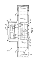
- Fig. 1 illustrates an exemplary sensor 10.
- the sensor 10 includes a housing 12 that encases the components of the sensor 10.
- the housing 12 helps protect the sensor 10 from dust and debris and other environmental hazards that may interfere with the functioning of the sensor 10.
- the sensor 10 also includes two mounts 14 and 16 protruding out of the housing 12.
- the mounts 14 and 16 provide a mechanism to allow the sensor 10 to be mounted onto a component or structure requiring stress monitoring, such as the frame of a vehicle.
- the mounts 14 and 16 are used as an interface to the component or structure so that any stress waves traveling through the component are transmitted to the sensor 10.
- the mounts 14 and 16 of the sensor 10 could be attached to a metal frame of a vehicle or a supporting beam of a building.
- the mounts 14 and 16 could be studs capable of attaching to a component with screws or bolts.
- the sensor 10 also includes a connector 18 that may be used to transmit sensor measurements to other control units that may activate devices or mechanisms based upon the data collected by the sensor 10.
- the support 20 contains the two mounts 14 and 16 and, in the embodiment shown, is constructed with each mount on one end of the support, causing the support 20 to behave like a tuning fork.
- the two mounts 14 and 16 act as tines of a tuning fork that are susceptible to stress waves, or vibrations. Stress waves or vibrations traveling through the beam or structure to which the sensor 10 is attached are transferred to the support 20 through the mounts 14 and 16.
- the stress waves or vibrations cause the support 20 to vibrate and distort.
- the support 20 is made from a flexible material or substance that is sensitive to stress waves. Aluminum, for example, may be used since it is light and flexible.
- the support 20 could also be constructed from steel or even high strength plastic.
- the thickness and composition of the support 20 determine the degree to which the support 20 distorts and, ultimately, the sensitivity of the sensor 10.
- the support may also contain more or less mounts placed in various configurations, other than at ends of the support in order to facilitate the distorting of the support 20.
- a circular support could be provided with three, four, or more mounts that may be attached to more than one beam or structure. Each mount will transmit stress waves from the beam or structure, to which it is attached, to the circular support.
- the support 20 also serves as a foundation for a semiconductor element 22.
- the semiconductor element 22 is attached to the support 20 such that the support 20 transfers any distortions caused by stress waves traveling through the support 20 to the semiconductor element 22.
- the semiconductor element 22 has similar flexibility.
- the semiconductor element 22 is attached along a surface of the support 20. In one embodiment, the semiconductor element 22 is attached flat to the surface of the support 20 so that the semiconductor element 22 will distort as the support 20 does.
- the semiconductor element 22 includes piezoresistors 24, 26, 28, and 30.
- the piezoresistors 24, 26, 28, and 30 are arranged in a Wheatstone-bridge configuration.
- the piezoresistors 24, 26, 28, and 30 are constructed with a material whose resistivity is influenced by the mechanical stress applied to the material such as piezoresistant material. Examples of piezoresistant materials include, but are not limited to, silicon, polycrystalline silicon, silica glass, zinc oxide, and germanium.
- the piezoresistors 24, 26, 28, and 30 are divided into two categories.
- the piezoresistors 24 and 28 are used as sensing piezoresistors and are arranged horizontally along the major or longitudinal axis of the semiconductor element 22.
- the piezoresistors 26 and 30 are used as reference piezoresistors, are smaller, and are arranged vertically or along the width of the semiconductor element 20.
- the reference piezoresistors 26 and 30 have less impedance than the sensing piezoresistors 24 and 28.
- the physical arrangement and characteristics of the two categories of piezoresistors make the sensing piezoresistors 24 and 28 more sensitive than the reference piezoresistors 26 and 30 to distortions of the semiconductor element 22 since they cover an area of the semiconductor element 22 that is more likely to distort in response to a stress wave passing through the support 20.
- the reference piezoresistors 26 and 30 are less sensitive to the distortions of the semiconductor element 22 since they cover less area of the semiconductor element 22 and are arranged closer to ends of the support 20 where the support 20 distorts less.
- the impedance of the sensing piezoresistors 24 and 28 will change more than the impedance of the reference piezoresistors 26 and 30.
- the difference between the changes of impedance of the two categories of piezoresistors can also be used to further estimate the characteristics of the impact or stress on the component that the sensor 10 is attached to.
- the semiconductor element 22 also contains input and output terminals 32, 34, 36, and 38.
- the input and output terminals 32, 34, 36, and 38 are used to apply and measure voltage and/or current passing through the piezoresistors 24, 26, 28, and 30.
- the support 20 may also be constructed from a semiconductor material and may directly contain the piezoresistors 24, 26, 28, and 30 rather than a separate semiconductor element 22 attached to the support 20. Any distortion of the semiconductor support created by stress waves traveling through the attached structure also causes the material of the embedded piezoresistors to distort.
- the semiconductor support may also contain input/output terminals used to apply and transmit voltage and/or charge flowing through the semiconductor support.
- Applying voltage, measuring current, and calculating resistance can all be performed by a processor such as an application specific integrated circuit ("ASIC") 40 attached to the semiconductor element 22.
- ASIC 40 is shown as being attached to a printed circuit board (“PCB”) 42 through the input and output terminals 44, 46, 48, and 50.
- PCB printed circuit board
- Other connections and even other calculating mechanisms may be used.
- a chip or microprocessor could also replace the ASIC 40.
- the ASIC 40 could also be eliminated from the sensor 10 and the output and input terminals 32, 34, 36, and 38 of the semiconductor element 22 could be directly coupled to the connector 18.
- the connector 18 may provide amplification or filtering to improve the characteristics of any data sent from the sensor 10 or received by the sensor 10, for example current or voltage values. However, the connector 18 does not process the data in order to deduce the meaning of the data such as to what degree the support 20 is stressed and distorted.
- the ASIC 40 may also act as a relay or amplifier for a sensed current measurement based on a constant application of voltage. The ASIC 40 could also process the sensed current of the piezoresistor arrangement and calculate a change in resistance, which could be used to further calculate a degree of stress applied to the support.
- Fig. 2 illustrates the sensor 10 of Fig. 1 from a front view.
- the connector 18, shown with solid lines, is protruding toward the viewer.
- Two ends of the two mounts 14 and 16 are also protruding toward the viewer.
- the PCB 42 and attached ASIC 40 and the semiconductor element 22 are also displayed in phantom lines situated beneath the connector 18.
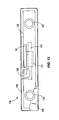
- Fig. 3 illustrates a second exemplary sensor 52 from a top view.
- the sensor 52 contains all of same components as the sensor 10, but the semiconductor element 22 is not located on the top surface of the support 20.
- the semiconductor element 22 is attached along the front edge of the support 20.
- the surface of the semiconductor element 22 containing the piezoresistors is positioned at a right angle to the ASIC 40 and PCB 42 rather than positioned parallel to the ASIC 40 and PCB 42 as in the sensor 10.
- the semiconductor element 22 may be placed on the back surface or edge of the support 20.
- the location of the semiconductor element 22 can be varied to adjust the functionality of the sensor.
- the position of the semiconductor element 22 can also be varied to change the size and dimensions of the sensor. For example, placing the semiconductor element 22 on the front edge of the support 20 reduces the thickness of the sensor.
- the semiconductor element 22 may also be placed in a location where it can be easily replaced or tested, if needed.
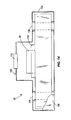
- Fig. 4 illustrates the sensor 52 from a front view. Since the semiconductor element 22 is positioned along the front edge of the support 20 the piezoresistors 24, 26, 28, and 30 contained within the semiconductor element 22 are seen when the sensor 52 is viewed from the front.
- the ASIC 40 and PCB 42 hinder the full view of the semiconductor element 22 since the semiconductor element 22 is positioned in a plane perpendicular to the plan containing the ASIC 40 and PCB 42.
- the connector 18 is shown in phantom lines and is protruding toward the viewer.
- Fig. 5 illustrates the semiconductor element 22 displayed in Figs. 1 - 4.
- the semiconductor element 22 contains the four piezoresistors 24, 26, 28, and 30 as well as the input and output terminals 32, 34, 36, and 38.
- the sensing piezoresistors 24 and 28 are arranged length-wise in the middle of the semiconductor element 22. Their position makes them more sensitive to distortions of the semiconductor element 22 than the reference piezoresistors 26 and 30 since they cover an area of the semiconductor element 22 that is more likely to distort in response to stress waves.
- the reference piezoresistors 26 and 30 are less sensitive to the distortions of the semiconductor element 22 since they cover less area of the semiconductor element 22 and are arranged closer to ends of the support 20 where the support 20 distorts less.
- the reference piezoresistors 26 and 30 may have higher impedance than the sensing piezoresistors 24 and 28. Other constructions are also possible. All four resistors may have identical impedance or their impedance may be varied to better utilize and categorize a reading from the sensor.
- Each terminal 32, 34, 36, and 38 of the semiconductor element 22 may have a designated data flow such as input only or output only or both may be bi-directional.
- the input and output terminals 32, 34, 36, and 38 may be configured to be coupled to a variety of devices including a PCB, a microprocessor, or a connector.
- Fig. 6 illustrates the sensor 10 shown in Figs. 1 and 2 mounted in a vehicle 60.
- the sensor 10 and the components of the vehicle 60 are not drawn to scale.
- the sensor 10 is illustrated without the housing 12, the connected ASIC 40 and PCB 42, and the connector 18.
- the vehicle 60 contains a side sill 62 and a B-pillar 63 on each side.
- the side sills 62 are positioned parallel to a surface that the vehicle 60 travels on and supports the side doors and windows.
- the B-pillars 63 are attached to the side sills 62 and protrude upward toward the roof of the vehicle 60.
- the B-pillars 63 may connect along the roof of the vehicle or may simply extend and connect to the roof.
- the sensor 10 is shown mounted on a B-pillar 63.
- a single sensor 10 is shown mounted to the side of the vehicle 60 located next to a driver seat 64 for illustration purposes only. In practical use, each side of the vehicle 60 may include a sensor 10.
- the sensor 10 may also be mounted to other structures of the vehicle 60 capable of transmitting stress waves such as the side sills 62, roof, or other supporting frames.
- the mounts 14 and 16 are connected to the B-pillar 63 with screws 70 and 72. As indicated earlier, the screws 70 and 72 could be replaced with bolts, rivets, or any other fastener.
- the mounts 14 and 16 could also be soldered or welded to the B-pillar 63. Other constructions are also possible depending on the composition and position of the mounts 14 and 16 and the structure to which the mounts 14 and 16 are attached.
- any stress waves traveling through the B-pillar 63 are transmitted to the sensor 10.
- Stress waves travel from the B-pillar 63 and through the mounts 14 and 16 to the support 20.
- the support 20 distorts according to the amplitude, frequency, or other characteristic of the stress waves, which also causes the semiconductor element 22 attached to the support 20 to distort.
- the distortion of the semiconductor element 22 causes the resistance of the piezoresistors 24, 26, 28, and 30 to change.
- the change in the resistance of the piezoresistors 24, 26, 28, and 30 can be processed by the ASIC or other processing device to monitor stress present in the B-pillar 63 of the vehicle 60. Changes in the resistance of the piezoresistors can indicate a collision or accident that may require the activation of safety restraint devices such as seatbelts or airbags.
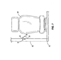
- Fig. 7 illustrates the sensor 10 mounted to a B-pillar 63 of a vehicle 60 from a rear view.
- the side sill 62 is shown supporting the B-pillar 63 that is positioned parallel and adjacent to the driver seat 64.
- the sensor 10 is illustrated mounted to the B-pillar 63 with the screw 70. Another screw may be used to mount the other end of the sensor 10 to the B-pillar 63 although it is not shown.
- Figs. 8 - 9 illustrates the support 20 of the sensor 10 distorted due to stress waves.
- the dashed lined illustrates the support 20 distorted from its original position, which is shown in solid lines.
- the support 20 is shown without the housing 12, the semiconductor element 22, the ASIC 40 and PCB 42, and connector 18.
- the stress waves cause the support 20 to distort into a U-shaped beam either upward toward the top of the sensor 10 or downward toward the bottom of the sensor 10.
- the semiconductor element 22 contains the piezoresistors 24, 26, 28, and 30 that also distort with the semiconductor element 22.
- the sensing piezoresistors 24 and 28 are distorted more than the reference piezoresistors 26 and 30 due to there position and size. Since the support 20 bends length-wise into a U-shape, the sensing piezoresistors 24 and 28 are distorted while the reference piezoresistors 26 and 30 are not. As sensing piezoresistors 24 and 28 distort, their associated impedance changes due to the physical change of the material of the sensing piezoresistors 24 and 28.
- the ASIC 40 (not shown) can monitor the change of impedance of the sensing piezoresistors 24 and 28 so that the safety mechanisms may be activated when appropriate.
- the impact of the accident causes stress waves to propagate through the vehicle structure 50 and to the attached sensor.
- a single sensor may be used to sense impact anywhere along the vehicle. It may be desirable, however, to place a sensor along each side of the vehicle 60 to reduce the travel distance and, therefore, also reduce the travel time of the stress waves. Such a configuration also increases the reaction time of the system. Using a sensor on each side of a vehicle also increases the sensitivity and accuracy of each sensor since the stress waves travel a shorter distance. This decreases the amount of time and the amount of material that the stress wave travels through. Certain characteristics of the waves may dissipate over time or as the waves travel through various media.
- the support 20 returns to its original shape after the stress waves have passed through it.
- the support 20 may be distorted to a point where it retains its distorted shape. In this case, the accident would likely cause damage to the vehicle that requires repair before the vehicle can be used again, and the sensor may also need to be repaired in this situation.
- the senor is paired with another sensor with different sensing principals to provide a hybrid impact sensor. Combining two different sensors that sense different variables in a single hybrid sensor helps increase the range, accuracy, and efficiency in detecting vehicle impact.
- Fig. 11 illustrates an exemplary hybrid sensor 75.
- the hybrid sensor 75 includes the sensor 10 and a pressure sensor 80.
- the pressure sensor 80 is attached to the PCB 42 and includes a door cavity pressure sensor that is configured to measure door cavity pressure changes that may occur during impact.
- the pressure sensor 80 may include one or more micromachined silicon door cavity pressure sensors, which are manufactured, among others, by Analog Devices and Motorola. Door cavity pressure sensors are well known in the art and, therefore, not described in detail.
- the pressure sensor 80 may also include other components such as an ASIC, input/output terminals, and the like.
- the senor 10 and the pressure sensor 80 are contained within the housing 12.
- the housing 12 may include an opening 82.
- the opening 82 may also be constructed to limit or prevent pressure changes due to changes in humidity or other air characteristics unrelated to changes due to impact.
- Fig. 12 illustrates another exemplary hybrid sensor 85.
- the hybrid sensor 85 includes the sensor 10 and an acceleration sensor 90.
- the acceleration sensor 90 is attached to the PCB 42 and includes an accelerometer configured to measure acceleration or deceleration of a vehicle or other object.
- the acceleration sensor 90 may include one or more micromachined silicon acceleration sensors like those manufactured by Analog Devices and Motorola among others. Acceleration sensors are well known in the art and, therefore, not described in detail.
- the acceleration sensor 90 may also include other components such as an ASIC, input/output terminals, and the like. As shown in Fig. 12, the sensor 10 and the acceleration sensor 90 are also contained within the housing 12.
- the hybrid sensors 75 and 85 may provide early impact detection, and, as described for the sensors 10 and 52, a single hybrid sensor 75 or 85 may be capable of detecting impact along an entire side of a vehicle.
- the dual sensing properties of the hybrid sensors 75 and 85 may also provide more accurate impact sensing, since one sensor can double-check the operation of the other sensor. For example, if the pressure sensor 80 or acceleration sensor 90 detects characteristics such as pressure changes or high rates of deceleration that may indicate impact while the sensor 10 does not detect corresponding stress waves indicating impact, safety equipment such as seat belt tensioning or air bags may not be activated.
- the multiple sensing properties may provide safing functionality to activate safety equipment when it is necessary and/or safe to do so.
- the hybrid sensors 75 and 85 may include multiple sensors 10 and multiple pressure sensors 80 and/or acceleration sensors 90.
- the hybrid sensors 75 and 85 may also include other types of sensors in place of or in addition to the pressure sensor 80 and/or acceleration sensor 90.
- the hybrid sensors 75 and 85 may include speed sensors, brakes sensors, steering wheel sensors, transmission sensors, and the like, to detect impact to a vehicle.
- the sensor 10 may also be replaced with the sensor 52, as described above, as well as other configurations.
- the pressure sensor 80 and acceleration sensor 90 may also be placed at different locations on the sensor 10.
- the pressure sensor 80 or acceleration sensor 90 may be attached to a separate PCB (not shown).
- the opening 82 in the housing 12 for the pressure sensor 80 may also be located in various locations and have various configurations.
- the sensor 10 may also be replaced with other stress wave sensors to create additional hybrid sensors.
- Figs. 13 and 14 illustrate a hybrid sensor 95 from a front and top view respectively.
- the hybrid sensor 95 includes the pressure sensor 80, as described above, and a magnetostrictive sensor 100.
- Magnetostrictive sensors useful in embodiments of the invention include sensors manufactured by Southwest Research Institute and are described in U.S. Patents 5,456,113; 5,457,994; and 5,767,766. Magnetostrictive sensors are configured to detect stress waves traveling through a structure by detecting variations in magnetization. Magnetostrictive sensors can actively or passively detect stress or strain to a structure.
- Active magnetostrictive sensors may introduce a stress wave with certain characteristics to a structure and may detect any modifications and/or reflections of the stress wave due to fractures or cracks in the structure. Modifications of the introduced stress waves may cause changes in magnetic flux detectable by a receiving coil of the sensor. Passive magnetostrictive sensors may monitor for stress waves introduced by structure cracking, breaking, impacts, or vibrations that also cause changes in magnetic flux detectable by a receiving coil of the sensor. As described for the sensors 10 and 52 above, magnetostrictive sensors 100 may be able to detect impacts fast and efficiently even if they are not located directly at the point of impact. The ability to sense impact over an extended area allows fewer magnetostrictive sensors 100 to be used to impact monitoring systems.
- a single magnetostrictive 100 sensor When used in vehicles, a single magnetostrictive 100 sensor may be employed on each side of the vehicle to detect impacts along the entire side of the vehicle.
- an independent sensor such as the pressure sensor 80
- the operation of the magnetostrictive sensor 100 can be verified or double-checked by the operation of the independent sensor.
- the independent sensor provides safing functionality for the magnetostrictive sensor so that safety equipment, which can often only be deployed once and may cause injury or damage if deployed unnecessarily, is only activated when required.
- the magnetostrictive sensor 100 and pressure sensor 80 may be encased within a housing 108.
- the housing 108 may also include an opening 109 for the pressure sensor 80.
- the housing 108 is constructed from an insulating material such as plastic.
- the housing 108 may also be constructed from aluminum.
- the positions of the magnetostrictive sensor 100 and the pressure sensor 80 and/or acceleration sensor 90 may be fixed by a potting material (not shown) that fills the interior of the housing 108.
- the magnetostrictive sensor 100 and pressure sensor 80 may also be attached to a support 102.
- the support 102 may be constructed of a ferromagnetic material that has a magnetostrictive property that causes physical and/or dimensional changes associated with variations in magnetism. Stress waves traveling through the support 102 may cause changes in magnetic flux detectable by the magnetostrictive sensor 100.
- the housing 108 may includes two mounts 104 and 106.
- the mounts 104 and 106 protrude may provide a mechanism for the hybrid sensor 95 to be attached onto a component or structure requiring stress monitoring such as the frame of a vehicle.
- the mounts 104 and 106 may also extend and be connected to the support 102 when present.
- the mounts 104 and 106 are used as an interface to the component or structure so that any stress waves traveling through the component are transmitted to the hybrid sensor 95.
- the mounts 104 and 106 of the hybrid sensor 95 could be attached to a metal frame of a vehicle or a supporting beam of a building.
- the hybrid sensor 95 may be mounted on an inner door panel with the pressure sensor 80 or opening 109 facing the door cavity.
- the hybrid sensor 95 may also be mounted on a reinforcing beam typically provided in door panels to increase door stiffness against intruding or impacting objects.
- the mounts 104 and 106 could be studs capable of attaching to a component with screws, bolts, or rivets.
- the hybrid sensor 95 may also include a connector 110 that may be used to transmit sensor measurements or detections to a control unit that may activate devices or mechanisms based upon the data collected by the hybrid sensor 95.
- Figs. 15 and 16 show another exemplary hybrid sensor 115 from a front and top view respectively.
- the hybrid sensor 115 includes the magnetostrictive sensor 100 and the acceleration sensor 90. As described for the hybrid sensor 95, positions of the magnetostrictive sensor 100 and acceleration sensor 90 may be fixed by a potting material (not shown) or by attaching the magnetostrictive sensor 100 and the acceleration sensor 90 to the support 102.
- the magnetostrictive sensor 100 and the acceleration sensor 90 are also encased within the housing 108, which includes the mounts 102 and 104.
- the hybrid sensor 115 may also include the connector 110.
- the hybrid sensors 95 and 115 may include multiple magnetostrictive sensors 100 and multiple pressure sensors 80 and/or acceleration sensors 90.
- the magnetostrictive sensor 100, pressure sensor 80, and acceleration sensor 90 may also be located in various configurations.
- the magnetostrictive sensors 100 are illustrated next to the pressure sensor 80 and acceleration sensor 90 in Figs. 13 and 15 respectively, other configurations are possible.
- the pressure sensor 80 or acceleration sensor 90 is positioned on top of the magnetostrictive sensor 100.
- the sensors may be placed on top of each other to decrease the size of the hybrid sensor 95 or 115.
- the sensors may also be located on separate supports or components.
- the opening 109 in the housing 108 for the pressure sensor 80 may also be located in various locations and have various configurations.
- the hybrid sensors 95 and 115 may also include other types of sensors in addition to or in place of the magnetostrictive sensor 100, the pressure sensor 80, and/or the acceleration sensor 90.
- an acoustic wave sensor is used in place of the magnetostrictive sensor 100.
- Acoustic wave sensors detect the properties of acoustic waves traveling through a component. If the component is modified (i.e., bent or dented during a collision) acoustic waves travel differently through the component. The detected changes of acoustic waves traveling through a component can be used to sense structure modifications and determine if impact has occurred.
Abstract
Description
- The present patent application claims priority to co-pending U.S. Patent Application Serial No. 10/983,547, filed November 8, 2004, which is a continuation-in-part of co-pending U.S. Patent Application Serial No. 10/866,386, filed on June 11, 2004, the entire contents of which are hereby incorporated by reference.
- Embodiments of the invention relate to impact sensors some of which detect stress waves and others which include at least two types of sensors.
- Vehicles are often equipped with impact sensors so that air bags and other safety restraints can be triggered, for example, during an accident. Most sensors, however, can only sense impacts within a close proximity of the sensor. Safety sensor systems often include numerous accelerometers and/or door cavity pressure sensors separately or in combination. Numerous sensors are often employed since a sensor must be directly hit during an accident in order to detect impact. The sensors are often placed where impacts are common. Even though multiple sensors are used in detection systems, certain types of impacts are still difficult for the systems to identify. For example, impacts with narrow objects such as poles often pose a challenge for detection systems unless the pole directly hits a sensor. Thus, unless sensors completely cover all sides of a vehicle, the chance that an accident will be missed by the detection system still exists.
- There is a need to provide sensors that can correctly detect an impact without having to be physically close to the point of contact.
- In one embodiment, the invention provides a sensor that can measure the strain waves or stress waves traveling through a vehicle structure caused by deformation of the structure due to impact in a crash. The sensor is mounted onto a suitable vehicle structure, for example, the B-pillar of the vehicle or a reinforcing beam inside the door of the vehicle. The range of the sensor is adequate to allow only a single sensor to be placed along each side of a vehicle. The sensor includes a sensitive support that distorts when stress waves travel through it. A semiconductor element is mounted on the support such that it is distorted with the support. The semiconductor element, e.g., a silicon beam, may contain piezoresistors arranged in a Wheatstone-bridge configuration. The impedance of the piezoresistors changes as the physical characteristics of the attached support change. The sensor also contains a circuit capable of sensing the impedance of the piezoresistors. The change of the sensed impedance can be used to detect stress waves. By detecting the stress waves caused by impact and not the direct impact itself, the sensor can detect impacts that occur remotely from the location of the sensor.
- In other embodiments, the stress wave sensor can be used to observe stress waves in other structures besides a vehicle structure. The sensor could be used to monitor stress applied to buildings or bridges or other components where unchecked stress strain can cause safety concerns. Any substance supporting the propagation of stress or force waves could be attached to the disclosed stress wave sensor. The material of the support contained within the sensor as well as the piezoresistant material used in the piezoresistors and semiconductor element can also be varied to create a specific sensor for specific types of stress waves.
- In another embodiment, the invention provides a hybrid impact sensor. The sensor may include a support containing one or more mounts. The sensor may also include a first sensor with first sensing properties, which is configured to generate a first output signal and a second sensor with second sensing properties, which is configured to generate a second output signal. The second sensing properties are different from the first sensing properties. A housing encases the first sensor and the second sensor.
- Another embodiment provides a method of sensing impact to a structure. The method may include providing a support with one or more mounts; providing a first sensor of a first sensing type; providing a second sensor of a second sensing type, wherein the second sensing type is different from the first sensing type; encasing the first sensor and the second sensor in a housing; generating a first output signal; and generating a second output signal.
- Additional embodiments provide a hybrid impact sensor. The sensor may include a support containing one or more mounts and a semiconductor element mounted to the support between the mounts. The semiconductor element contains input and output terminals and a plurality of piezoresistors. Each piezoresistor has an impedance. The sensor may also include a circuit configured to be coupled to the input and output terminals of the semiconductor element. The circuit is capable of sensing the impedance of the plurality of piezoresistors. The sensor also includes a pressure sensor configured to generate a pressure signal. Yet another embodiment provides a method for sensing impact to a structure. The method may include providing a support with one or more mounts; attaching a semiconductor element containing a plurality of piezoresistors, each having impedance, to the support; connecting the support to the structure with the mounts of the support; providing a pressure sensor configured to generate a pressure signal; encasing the support and the pressure sensor in a housing; sensing the impedance of the plurality of piezoresistors; and sensing the pressure signal.
- Additional embodiments further provide a hybrid impact sensor. The sensor may include a support containing one or more mounts; a semiconductor element mounted to the support between the mounts and containing input and output terminals and a plurality of piezoresistors each piezoresistor having an impedance; a circuit configured to be coupled to the input and output terminals of the plurality of piezoresistors and capable of sensing the impedance of the plurality of piezoresistors; and an acceleration sensor configured to generate an acceleration signal.
- Another embodiment provides a method for sensing impact to a structure. The method may include providing a support with one or more mounts; attaching a semiconductor element to a support, the element containing a plurality of piezoresistors, each having an impedance; connecting the support to the structure with the mounts of the support; providing an acceleration sensor configured to generate an acceleration signal; encasing the support and the pressure sensor in a housing; sensing the impedance of the plurality of piezoresistors; and sensing the acceleration signal.
- Yet another embodiment provides a hybrid impact sensor. The impact sensor may include a support containing one or more mounts and a magnetostrictive sensor. The magnetostrictive sensor is configured to provide a stress wave signal. A pressure sensor configured to provide a pressure signal is also included in the impact sensor. A housing encases the magnetostrictive sensor and the pressure sensor. Instead of a pressure sensor, an acceleration sensor may also be used.
- Additional embodiments provide a method for sensing impact to a structure. The method may include providing a support with one or more mounts; providing a magnetostrictive sensor configured to generate a stress wave signal; providing a pressure sensor configured to generate a pressure signal; encasing the magnetostrictive sensor and the pressure sensor in a housing; sensing the stress wave signal; and sensing the pressure signal. If an acceleration sensor is used in place of the pressure sensor, the method includes sensing an acceleration signal.
- Other features and advantages of the invention will become apparent to those skilled in the art upon review of the detailed description, claims, and drawings.
- In the drawings:
- Fig. 1
- is a top view of a first exemplary embodiment of the invention.
- Fig. 2
- is a front view of the exemplary embodiment illustrated in Fig. 1.
- Fig. 3
- is a top view of a second exemplary embodiment of the invention.
- Fig. 4
- is a front view of the second exemplary illustrated in Fig. 3.
- Fig. 5
- is a schematic illustration of a semiconductor element suitable for use in the embodiments illustrated in Figs. 13.
- Fig. 6
- is a top-view illustration of the sensor of Fig. 1 mounted to a vehicle structure.
- Fig. 7
- is a rear-view illustration of the sensor of Fig. 1 mounted to a vehicle structure.
- Figs. 8 and 9
- illustrate exemplary directions of bending of the support of the sensor of Fig. 1 due to stress waves traveling through it.
- Fig. 10
- illustrates the support and semiconductor element of the sensor of Fig. 1 bending due to stress waves traveling through it.
- Fig. 11
- is a top view of an exemplary embodiment of the invention.
- Fig. 12
- is a top view of another exemplary embodiment of the invention.
- Fig. 13
- is a front view of another exemplary embodiment of the invention.
- Fig. 14
- is a top view of the exemplary embodiment illustrated in Fig. 13.
- Fig. 15
- is a front view of yet another exemplary embodiment of the invention.
- Fig. 16
- is a top view of the exemplary embodiment illustrated in Fig. 15.
- It is to be understood that the invention is not limited in its application to the details of construction and the arrangement of components set forth in the following description or illustrated in the drawings. The invention is capable of other embodiments and of being practiced or of being carried out in various ways. Also, it is to be understood that the phraseology and terminology used herein is for the purpose of description and should not be regarded as limiting. The use of "including," "comprising," or "having" and variations thereof herein is meant to encompass the items listed thereafter and equivalents thereof as well as additional items. Unless limited otherwise, the terms "connected," "coupled," and "mounted," and variations thereof herein are used broadly and encompass direct and indirect connections, couplings, and mountings. In addition, the terms "connected" and "coupled" and variations thereof are not restricted to physical or mechanical connections or couplings.
- Fig. 1 illustrates an
exemplary sensor 10. Thesensor 10 includes ahousing 12 that encases the components of thesensor 10. Thehousing 12 helps protect thesensor 10 from dust and debris and other environmental hazards that may interfere with the functioning of thesensor 10. Thesensor 10 also includes twomounts housing 12. Themounts sensor 10 to be mounted onto a component or structure requiring stress monitoring, such as the frame of a vehicle. Themounts sensor 10. Themounts sensor 10 could be attached to a metal frame of a vehicle or a supporting beam of a building. Alternatively, themounts sensor 10 also includes aconnector 18 that may be used to transmit sensor measurements to other control units that may activate devices or mechanisms based upon the data collected by thesensor 10. - Located inside the
housing 12 is asupport 20. Thesupport 20 contains the twomounts support 20 to behave like a tuning fork. The two mounts 14 and 16 act as tines of a tuning fork that are susceptible to stress waves, or vibrations. Stress waves or vibrations traveling through the beam or structure to which thesensor 10 is attached are transferred to thesupport 20 through themounts - The stress waves or vibrations cause the
support 20 to vibrate and distort. Thesupport 20 is made from a flexible material or substance that is sensitive to stress waves. Aluminum, for example, may be used since it is light and flexible. Thesupport 20 could also be constructed from steel or even high strength plastic. The thickness and composition of thesupport 20 determine the degree to which thesupport 20 distorts and, ultimately, the sensitivity of thesensor 10. The support may also contain more or less mounts placed in various configurations, other than at ends of the support in order to facilitate the distorting of thesupport 20. For example, a circular support could be provided with three, four, or more mounts that may be attached to more than one beam or structure. Each mount will transmit stress waves from the beam or structure, to which it is attached, to the circular support. - The
support 20 also serves as a foundation for asemiconductor element 22. Thesemiconductor element 22 is attached to thesupport 20 such that thesupport 20 transfers any distortions caused by stress waves traveling through thesupport 20 to thesemiconductor element 22. Just as thesupport 20 is flexible in order to distort due to the propagation of stress waves, thesemiconductor element 22 has similar flexibility. Thesemiconductor element 22 is attached along a surface of thesupport 20. In one embodiment, thesemiconductor element 22 is attached flat to the surface of thesupport 20 so that thesemiconductor element 22 will distort as thesupport 20 does. - The
semiconductor element 22 includespiezoresistors piezoresistors piezoresistors piezoresistors piezoresistors semiconductor element 22. Thepiezoresistors semiconductor element 20. Thereference piezoresistors reference piezoresistors semiconductor element 22 since they cover an area of thesemiconductor element 22 that is more likely to distort in response to a stress wave passing through thesupport 20. Likewise, thereference piezoresistors semiconductor element 22 since they cover less area of thesemiconductor element 22 and are arranged closer to ends of thesupport 20 where thesupport 20 distorts less. When thesupport 20 and the attachedsemiconductor element 22 are distorted by stress waves, the impedance of the sensing piezoresistors 24 and 28 will change more than the impedance of thereference piezoresistors sensor 10 is attached to. - The
semiconductor element 22 also contains input andoutput terminals output terminals piezoresistors - The
support 20 may also be constructed from a semiconductor material and may directly contain thepiezoresistors separate semiconductor element 22 attached to thesupport 20. Any distortion of the semiconductor support created by stress waves traveling through the attached structure also causes the material of the embedded piezoresistors to distort. The semiconductor support may also contain input/output terminals used to apply and transmit voltage and/or charge flowing through the semiconductor support. - Applying voltage, measuring current, and calculating resistance can all be performed by a processor such as an application specific integrated circuit ("ASIC") 40 attached to the
semiconductor element 22. TheASIC 40 is shown as being attached to a printed circuit board ("PCB") 42 through the input andoutput terminals ASIC 40. TheASIC 40 could also be eliminated from thesensor 10 and the output andinput terminals semiconductor element 22 could be directly coupled to theconnector 18. By directly coupling thesemiconductor element 22 to theconnector 18 the processing of the measurements taken by the sensor 10 (i.e., the calculating of resistance) can be carried out outside of thesensor 10 at a remote control unit. Theconnector 18 may provide amplification or filtering to improve the characteristics of any data sent from thesensor 10 or received by thesensor 10, for example current or voltage values. However, theconnector 18 does not process the data in order to deduce the meaning of the data such as to what degree thesupport 20 is stressed and distorted. TheASIC 40 may also act as a relay or amplifier for a sensed current measurement based on a constant application of voltage. TheASIC 40 could also process the sensed current of the piezoresistor arrangement and calculate a change in resistance, which could be used to further calculate a degree of stress applied to the support. - Fig. 2 illustrates the
sensor 10 of Fig. 1 from a front view. Theconnector 18, shown with solid lines, is protruding toward the viewer. Two ends of the twomounts PCB 42 and attachedASIC 40 and thesemiconductor element 22 are also displayed in phantom lines situated beneath theconnector 18. The input andoutput terminals 44 and 46 (input andoutput terminals PCB 42 and the input andoutput terminals semiconductor element 22 are also shown in phantom lines along with thesupport 20 and the twomounts - Fig. 3 illustrates a second
exemplary sensor 52 from a top view. Thesensor 52 contains all of same components as thesensor 10, but thesemiconductor element 22 is not located on the top surface of thesupport 20. As can be seen in Fig. 3, thesemiconductor element 22 is attached along the front edge of thesupport 20. The surface of thesemiconductor element 22 containing the piezoresistors is positioned at a right angle to theASIC 40 andPCB 42 rather than positioned parallel to theASIC 40 andPCB 42 as in thesensor 10. Similarly, thesemiconductor element 22 may be placed on the back surface or edge of thesupport 20. The location of thesemiconductor element 22 can be varied to adjust the functionality of the sensor. The position of thesemiconductor element 22 can also be varied to change the size and dimensions of the sensor. For example, placing thesemiconductor element 22 on the front edge of thesupport 20 reduces the thickness of the sensor. Thesemiconductor element 22 may also be placed in a location where it can be easily replaced or tested, if needed. - Fig. 4 illustrates the
sensor 52 from a front view. Since thesemiconductor element 22 is positioned along the front edge of thesupport 20 thepiezoresistors semiconductor element 22 are seen when thesensor 52 is viewed from the front. - When viewed from the front, the
ASIC 40 andPCB 42 hinder the full view of thesemiconductor element 22 since thesemiconductor element 22 is positioned in a plane perpendicular to the plan containing theASIC 40 andPCB 42. Theconnector 18 is shown in phantom lines and is protruding toward the viewer. - Fig. 5 illustrates the
semiconductor element 22 displayed in Figs. 1 - 4. Thesemiconductor element 22 contains the fourpiezoresistors output terminals semiconductor element 22. Their position makes them more sensitive to distortions of thesemiconductor element 22 than thereference piezoresistors semiconductor element 22 that is more likely to distort in response to stress waves. Thereference piezoresistors semiconductor element 22 since they cover less area of thesemiconductor element 22 and are arranged closer to ends of thesupport 20 where thesupport 20 distorts less. Thereference piezoresistors semiconductor element 22 may have a designated data flow such as input only or output only or both may be bi-directional. The input andoutput terminals - Fig. 6 illustrates the
sensor 10 shown in Figs. 1 and 2 mounted in avehicle 60. Thesensor 10 and the components of thevehicle 60 are not drawn to scale. For the sake of clarity, thesensor 10 is illustrated without thehousing 12, the connectedASIC 40 andPCB 42, and theconnector 18. Thevehicle 60 contains aside sill 62 and a B-pillar 63 on each side. Theside sills 62 are positioned parallel to a surface that thevehicle 60 travels on and supports the side doors and windows. The B-pillars 63 are attached to theside sills 62 and protrude upward toward the roof of thevehicle 60. The B-pillars 63 may connect along the roof of the vehicle or may simply extend and connect to the roof. Thesensor 10 is shown mounted on a B-pillar 63. Asingle sensor 10 is shown mounted to the side of thevehicle 60 located next to adriver seat 64 for illustration purposes only. In practical use, each side of thevehicle 60 may include asensor 10. Thesensor 10 may also be mounted to other structures of thevehicle 60 capable of transmitting stress waves such as theside sills 62, roof, or other supporting frames. Themounts pillar 63 withscrews screws mounts pillar 63. Other constructions are also possible depending on the composition and position of themounts mounts - Once the
sensor 10 has been attached to the B-pillar 63, any stress waves traveling through the B-pillar 63 are transmitted to thesensor 10. Stress waves travel from the B-pillar 63 and through themounts support 20. Thesupport 20 distorts according to the amplitude, frequency, or other characteristic of the stress waves, which also causes thesemiconductor element 22 attached to thesupport 20 to distort. The distortion of thesemiconductor element 22 causes the resistance of thepiezoresistors piezoresistors pillar 63 of thevehicle 60. Changes in the resistance of the piezoresistors can indicate a collision or accident that may require the activation of safety restraint devices such as seatbelts or airbags. - Fig. 7 illustrates the
sensor 10 mounted to a B-pillar 63 of avehicle 60 from a rear view. Theside sill 62 is shown supporting the B-pillar 63 that is positioned parallel and adjacent to thedriver seat 64. Thesensor 10 is illustrated mounted to the B-pillar 63 with thescrew 70. Another screw may be used to mount the other end of thesensor 10 to the B-pillar 63 although it is not shown. - Figs. 8 - 9 illustrates the
support 20 of thesensor 10 distorted due to stress waves. The dashed lined illustrates thesupport 20 distorted from its original position, which is shown in solid lines. For purpose of illustration thesupport 20 is shown without thehousing 12, thesemiconductor element 22, theASIC 40 andPCB 42, andconnector 18. The stress waves cause thesupport 20 to distort into a U-shaped beam either upward toward the top of thesensor 10 or downward toward the bottom of thesensor 10. - Referring to Fig. 10, as the
support 20 distorts so does the attachedsemiconductor element 22. Thesemiconductor element 22 contains thepiezoresistors semiconductor element 22. As shown in Fig. 10, the sensing piezoresistors 24 and 28 are distorted more than thereference piezoresistors support 20 bends length-wise into a U-shape, the sensing piezoresistors 24 and 28 are distorted while thereference piezoresistors piezoresistors - In the case of an accident at any point along a side of the
vehicle 60, the impact of the accident causes stress waves to propagate through thevehicle structure 50 and to the attached sensor. If the structure of thevehicle 60 is integral or unitary, a single sensor may be used to sense impact anywhere along the vehicle. It may be desirable, however, to place a sensor along each side of thevehicle 60 to reduce the travel distance and, therefore, also reduce the travel time of the stress waves. Such a configuration also increases the reaction time of the system. Using a sensor on each side of a vehicle also increases the sensitivity and accuracy of each sensor since the stress waves travel a shorter distance. This decreases the amount of time and the amount of material that the stress wave travels through. Certain characteristics of the waves may dissipate over time or as the waves travel through various media. - The
support 20 returns to its original shape after the stress waves have passed through it. In severe accidents or collision thesupport 20 may be distorted to a point where it retains its distorted shape. In this case, the accident would likely cause damage to the vehicle that requires repair before the vehicle can be used again, and the sensor may also need to be repaired in this situation. - In some embodiments, the sensor is paired with another sensor with different sensing principals to provide a hybrid impact sensor. Combining two different sensors that sense different variables in a single hybrid sensor helps increase the range, accuracy, and efficiency in detecting vehicle impact.
- Fig. 11 illustrates an
exemplary hybrid sensor 75. Thehybrid sensor 75 includes thesensor 10 and apressure sensor 80. In some embodiments, thepressure sensor 80 is attached to thePCB 42 and includes a door cavity pressure sensor that is configured to measure door cavity pressure changes that may occur during impact. Thepressure sensor 80 may include one or more micromachined silicon door cavity pressure sensors, which are manufactured, among others, by Analog Devices and Motorola. Door cavity pressure sensors are well known in the art and, therefore, not described in detail. Thepressure sensor 80 may also include other components such as an ASIC, input/output terminals, and the like. - As shown in Fig. 11, the
sensor 10 and thepressure sensor 80 are contained within thehousing 12. In order for thepressure sensor 80 to measure pressure changes, thehousing 12 may include anopening 82. Theopening 82 may also be constructed to limit or prevent pressure changes due to changes in humidity or other air characteristics unrelated to changes due to impact. - Fig. 12 illustrates another
exemplary hybrid sensor 85. Thehybrid sensor 85 includes thesensor 10 and anacceleration sensor 90. In some embodiments, theacceleration sensor 90 is attached to thePCB 42 and includes an accelerometer configured to measure acceleration or deceleration of a vehicle or other object. Theacceleration sensor 90 may include one or more micromachined silicon acceleration sensors like those manufactured by Analog Devices and Motorola among others. Acceleration sensors are well known in the art and, therefore, not described in detail. Theacceleration sensor 90 may also include other components such as an ASIC, input/output terminals, and the like. As shown in Fig. 12, thesensor 10 and theacceleration sensor 90 are also contained within thehousing 12. - The
hybrid sensors sensors single hybrid sensor hybrid sensors pressure sensor 80 oracceleration sensor 90 detects characteristics such as pressure changes or high rates of deceleration that may indicate impact while thesensor 10 does not detect corresponding stress waves indicating impact, safety equipment such as seat belt tensioning or air bags may not be activated. The multiple sensing properties may provide safing functionality to activate safety equipment when it is necessary and/or safe to do so. - It should be understood that the
hybrid sensors multiple sensors 10 andmultiple pressure sensors 80 and/oracceleration sensors 90. Thehybrid sensors pressure sensor 80 and/oracceleration sensor 90. For example, thehybrid sensors sensor 10 may also be replaced with thesensor 52, as described above, as well as other configurations. Thepressure sensor 80 andacceleration sensor 90 may also be placed at different locations on thesensor 10. For example, thepressure sensor 80 oracceleration sensor 90 may be attached to a separate PCB (not shown). Theopening 82 in thehousing 12 for thepressure sensor 80 may also be located in various locations and have various configurations. - The
sensor 10 may also be replaced with other stress wave sensors to create additional hybrid sensors. Figs. 13 and 14 illustrate ahybrid sensor 95 from a front and top view respectively. Thehybrid sensor 95 includes thepressure sensor 80, as described above, and amagnetostrictive sensor 100. Magnetostrictive sensors useful in embodiments of the invention include sensors manufactured by Southwest Research Institute and are described in U.S. Patents 5,456,113; 5,457,994; and 5,767,766. Magnetostrictive sensors are configured to detect stress waves traveling through a structure by detecting variations in magnetization. Magnetostrictive sensors can actively or passively detect stress or strain to a structure. Active magnetostrictive sensors may introduce a stress wave with certain characteristics to a structure and may detect any modifications and/or reflections of the stress wave due to fractures or cracks in the structure. Modifications of the introduced stress waves may cause changes in magnetic flux detectable by a receiving coil of the sensor. Passive magnetostrictive sensors may monitor for stress waves introduced by structure cracking, breaking, impacts, or vibrations that also cause changes in magnetic flux detectable by a receiving coil of the sensor. As described for thesensors magnetostrictive sensors 100 may be able to detect impacts fast and efficiently even if they are not located directly at the point of impact. The ability to sense impact over an extended area allows fewermagnetostrictive sensors 100 to be used to impact monitoring systems. When used in vehicles, asingle magnetostrictive 100 sensor may be employed on each side of the vehicle to detect impacts along the entire side of the vehicle. When paired with an independent sensor, such as thepressure sensor 80, the operation of themagnetostrictive sensor 100 can be verified or double-checked by the operation of the independent sensor. The independent sensor provides safing functionality for the magnetostrictive sensor so that safety equipment, which can often only be deployed once and may cause injury or damage if deployed unnecessarily, is only activated when required. - The
magnetostrictive sensor 100 andpressure sensor 80 may be encased within ahousing 108. Thehousing 108 may also include anopening 109 for thepressure sensor 80. In some embodiments, thehousing 108 is constructed from an insulating material such as plastic. Thehousing 108 may also be constructed from aluminum. - The positions of the
magnetostrictive sensor 100 and thepressure sensor 80 and/oracceleration sensor 90 may be fixed by a potting material (not shown) that fills the interior of thehousing 108. Themagnetostrictive sensor 100 andpressure sensor 80 may also be attached to asupport 102. Thesupport 102 may be constructed of a ferromagnetic material that has a magnetostrictive property that causes physical and/or dimensional changes associated with variations in magnetism. Stress waves traveling through thesupport 102 may cause changes in magnetic flux detectable by themagnetostrictive sensor 100. - The
housing 108 may includes twomounts mounts hybrid sensor 95 to be attached onto a component or structure requiring stress monitoring such as the frame of a vehicle. Themounts support 102 when present. - The
mounts hybrid sensor 95. Themounts hybrid sensor 95 could be attached to a metal frame of a vehicle or a supporting beam of a building. In some embodiments, thehybrid sensor 95 may be mounted on an inner door panel with thepressure sensor 80 oropening 109 facing the door cavity. Thehybrid sensor 95 may also be mounted on a reinforcing beam typically provided in door panels to increase door stiffness against intruding or impacting objects. Alternatively, themounts - The
hybrid sensor 95 may also include aconnector 110 that may be used to transmit sensor measurements or detections to a control unit that may activate devices or mechanisms based upon the data collected by thehybrid sensor 95. - Figs. 15 and 16 show another exemplary
hybrid sensor 115 from a front and top view respectively. Thehybrid sensor 115 includes themagnetostrictive sensor 100 and theacceleration sensor 90. As described for thehybrid sensor 95, positions of themagnetostrictive sensor 100 andacceleration sensor 90 may be fixed by a potting material (not shown) or by attaching themagnetostrictive sensor 100 and theacceleration sensor 90 to thesupport 102. Themagnetostrictive sensor 100 and theacceleration sensor 90 are also encased within thehousing 108, which includes themounts hybrid sensor 115 may also include theconnector 110. - It should be understood that the
hybrid sensors magnetostrictive sensors 100 andmultiple pressure sensors 80 and/oracceleration sensors 90. Themagnetostrictive sensor 100,pressure sensor 80, andacceleration sensor 90 may also be located in various configurations. Although themagnetostrictive sensors 100 are illustrated next to thepressure sensor 80 andacceleration sensor 90 in Figs. 13 and 15 respectively, other configurations are possible. In some embodiments, thepressure sensor 80 oracceleration sensor 90 is positioned on top of themagnetostrictive sensor 100. The sensors may be placed on top of each other to decrease the size of thehybrid sensor opening 109 in thehousing 108 for thepressure sensor 80 may also be located in various locations and have various configurations. - It should also be understood that the
hybrid sensors magnetostrictive sensor 100, thepressure sensor 80, and/or theacceleration sensor 90. In some embodiments, an acoustic wave sensor is used in place of themagnetostrictive sensor 100. Acoustic wave sensors detect the properties of acoustic waves traveling through a component. If the component is modified (i.e., bent or dented during a collision) acoustic waves travel differently through the component. The detected changes of acoustic waves traveling through a component can be used to sense structure modifications and determine if impact has occurred. - Various features and advantages of the invention are set forth in the following claims.
Claims (59)
- A method of sensing stress waves in a component (60 and 62), the method comprising:providing a support 20 with at least one mount (14 and 16);attaching a semiconductor element (22) containing a plurality of piezoresistors (24, 26, 28, and 30), each having impedance, to the support;connecting the support to the component with the at least one mount of the support; andsensing impedance of the plurality of piezoresistors.
- The method as claimed in claim 1, wherein attaching the semiconductor element includes mounting the semiconductor element along an entire surface of the support such that stress waves traveling through the support distort the semiconductor element.
- The method as claimed in claim 1, further comprising transmitting data from the plurality of piezoresistors to a control unit.
- The method as claimed in claim 1, further comprising providing a plurality of piezoresistors including sensing piezoresistors (24 and 28) and reference piezoresistors (26 and 30).
- The method as claimed in claim 4, wherein the reference piezoresistors have a different impedance than the sensing piezoresistors.
- The method as claimed in claim 1, wherein the at least one mount of the support is located at an end of the support.
- The method as claimed in claim 1, further comprising providing a circuit (40) configured to be coupled to input and output terminals (32, 34, 36, and 38) of the semiconductor element.
- The method as claimed in claim 7, further comprising mounting the circuit on a printed circuit board (42).
- The method as claimed in claim 8, further comprising mounting a pressure sensor (80) on the printed circuit board.
- The method as claimed in claim 8, further comprising mounting an acceleration sensor (90) on the printed circuit board.
- The method as claimed in claim 1, further comprising providing a pressure sensor (80) configured to generate a pressure signal.
- The method as claimed in claim 11, further comprising attaching the pressure sensor to the support.
- The method as claimed in claim 11, further comprising encasing the pressure sensor and the support in a housing (12).
- The method as claimed in claim 13, further comprising providing an opening (82) in the housing for the pressure sensor.
- The method as claimed in claim 11, further comprising detecting pressure within a door cavity of a vehicle.
- The method as claimed in claim 1, further comprising providing an acceleration sensor (90) configured to generate an acceleration signal.
- The method as claimed in claim 16, further comprising attaching the acceleration sensor to the support.
- The method as claimed in claim 16, further comprising encasing the acceleration sensor and the support in a housing (12).
- A system of sensing stress waves in a component (60 and 62), the system comprising:a support 20 with at least one mount (14 and 16) and configured to be attached to the component;a plurality of piezoresistors (24, 26, 28, and 30) each with an impedance;a semiconductor element (22) containing the plurality of piezoresistors and configured to be attached to the support; anda circuit (40) configured to be coupled to input and output terminals (32, 34, 36, and 38) of the semiconductor element and to sense impedance of the plurality of piezoresistors.
- The system as claimed in claim 19, wherein the plurality of piezoresistors includes reference piezoresistors (26 and 30) and sensing piezoresistors (24 and 28).
- The system as claimed in claim 20, wherein the reference piezoresistors have a different impedance than the sensing piezoresistors.
- The system as claimed in claim 19, wherein the support is configured to receive stress waves traveling through the component.
- The system as claimed in claim 19, wherein the semiconductor element is configured to be mounted along an entire surface of the support such that stress waves that travel through the support distort the semiconductor element.
- The system as claimed in claim 19, wherein the circuit is configured to be mounted to a printed circuit board (42).
- The system as claimed in claim 24, further comprising a pressure sensor (80) attached to the printed circuit board.
- The system as claimed in claim 24, further comprising an acceleration sensor (90) attached to the printed circuit board.
- The system as claimed in claim 19, further comprising a connector (18) configured to be coupled to the circuit and to transmit data to and from the circuit without processing the data.
- The system as claimed in claim 19, wherein the at least one mount of the support is located at an end of the support.
- The system as claimed in claim 19, wherein the at least one mount of the support is configured to allow stress waves traveling through the component to also travel through the support.
- The system as claimed in claim 19, further comprising a pressure sensor (80) configured to generate a pressure signal.
- The system as claimed in claim 30, wherein the pressure sensor is attached to the support.
- The system as claimed in claim 30, further comprising a housing (12) encasing the support and the pressure sensor.
- The system as claimed in claim 32, wherein the housing includes an opening (82) for the pressure sensor.
- The system as claimed in claim 30, wherein the pressure sensor is configured to detect pressure within a door cavity of a vehicle.
- The system as claimed in claim 30, wherein the circuit is further configured to be coupled to the pressure sensor and to sense the pressure signal.
- The system as claimed in claim 19, further comprising an acceleration sensor (90) configured to generate an acceleration signal.
- The system as claimed in claim 36, wherein the acceleration sensor is attached to the support.
- The system as claimed in claim 36, further comprising a housing (12) encasing the support and the acceleration sensor.
- The system as claimed in claim 36, wherein the circuit is further configured to be coupled to the acceleration sensor and to sense the acceleration signal.
- A hybrid impact sensor (75, 85, 95, and 115) comprising:a first sensor with first sensing properties and configured to generate a first output signal, wherein the first sensor includes at least one of a sensor (10) including a semiconductor element (22) containing input and output terminals (32, 34, 36, and 38) and a plurality of piezoresistors (24, 26, 28, and 30), wherein each piezoresistor has an impedance, and a circuit (40) configured to be coupled to the input and output terminals of the semiconductor element and capable of sensing the impedance of the plurality of piezoresistors; a magnetostrictive sensor (100); and an acoustic wave sensor.a second sensor with second sensing properties and configured to generate a second output signal, wherein the second sensing properties are different from the first sensing properties and wherein the second sensor includes at least one of an acceleration sensor (90) and a pressure sensor (80);a housing (12 and 108) encasing the first sensor and the second sensor; andat least one mount (14, 16, 104, and 106).
- A hybrid impact sensor as claimed in claim 40, further comprising a connector (18 and 110) configured to be coupled to at least one of the first sensor, the second sensor, and a control unit.
- A hybrid impact sensor as claimed in claim 41, wherein the connector is further configured to output at least one of the first sensor signal and the second signal to the control unit.
- A hybrid impact sensor as claimed in claim 40, wherein the at least one mount is configured to be attached to a component of a vehicle (60).
- A hybrid impact sensor as claimed in claim 40, further comprising a support (20 and 102).
- A hybrid impact sensor as claimed in claim 44, wherein the first sensor is attached to the support.
- A hybrid impact sensor as claimed in claim 44, wherein the second sensor is attached to the support.
- A hybrid impact sensor as claimed in claim 40, wherein the second sensor is attached to the first sensor.
- A hybrid impact sensor as claimed in claim 44, wherein the at least one mount is located at an end of the support.
- A hybrid impact sensor as claimed in claim 40, wherein the housing includes an opening (82 and 109) for the second sensor.
- A hybrid impact sensor as claimed in claim 40, wherein the second sensor is configured to detect pressure within a vehicle door cavity.
- A method of sensing impact to a component (60 and 62), the method comprising:providing a first sensor of a first sensing type, wherein the first sensor includes at least one of a sensor (10) including a semiconductor element (22) containing input and output terminals (32, 34, 36, and 38) and a plurality of piezoresistors (24, 26, 28, and 30), wherein each piezoresistor has an impedance, and a circuit (40) configured to be coupled to the input and output terminals of the semiconductor element and capable of sensing theimpedance of the plurality of piezoresistors; a magnetostrictive sensor (100); and an acoustic wave sensor;providing a second sensor of a second sensing type, wherein the second sensing type is different from the first sensing type and wherein the second sensor includes at least one of an acceleration sensor (90) and a pressure sensor (80);encasing the first sensor and the second sensor in a housing (12 and 108);providing at least one mount (14, 16, 104, and 106);generating a first output signal; andgenerating a second output signal.
- A method as claimed in claim 51, further comprising attaching the at least one mount to a component of a vehicle (60).
- A method as claimed in claim 51, further comprising providing a support (20 and 102).
- A method as claimed in claim 53, further comprising attaching the first sensor to the support.
- A method as claimed in claim 53, further comprising attaching the second sensor to the support.
- A method as claimed in claim 51, further comprising attaching the second sensor to the first sensor.
- A method as claimed in claim 53, further comprising placing the at least one mount at an end of the support.
- A method as claimed in claim 51, further comprising providing an opening (82 and 109) in the housing.
- A method as claimed in claim 51, further comprising detecting pressure within a vehicle door cavity.
Priority Applications (1)
| Application Number | Priority Date | Filing Date | Title |
|---|---|---|---|
| EP09004540A EP2085270A1 (en) | 2004-06-11 | 2005-06-07 | Hybrid impact sensor |
Applications Claiming Priority (4)
| Application Number | Priority Date | Filing Date | Title |
|---|---|---|---|
| US866386 | 1992-04-10 | ||
| US10/866,386 US7188511B2 (en) | 2004-06-11 | 2004-06-11 | Stress wave sensor |
| US983547 | 2004-11-08 | ||
| US10/983,547 US7231803B2 (en) | 2004-06-11 | 2004-11-08 | Hybrid impact sensor |
Related Child Applications (1)
| Application Number | Title | Priority Date | Filing Date |
|---|---|---|---|
| EP09004540A Division EP2085270A1 (en) | 2004-06-11 | 2005-06-07 | Hybrid impact sensor |
Publications (2)
| Publication Number | Publication Date |
|---|---|
| EP1604870A2 true EP1604870A2 (en) | 2005-12-14 |
| EP1604870A3 EP1604870A3 (en) | 2008-05-21 |
Family
ID=34937268
Family Applications (2)
| Application Number | Title | Priority Date | Filing Date |
|---|---|---|---|
| EP09004540A Withdrawn EP2085270A1 (en) | 2004-06-11 | 2005-06-07 | Hybrid impact sensor |
| EP05012189A Withdrawn EP1604870A3 (en) | 2004-06-11 | 2005-06-07 | Hybrid impact sensor |
Family Applications Before (1)
| Application Number | Title | Priority Date | Filing Date |
|---|---|---|---|
| EP09004540A Withdrawn EP2085270A1 (en) | 2004-06-11 | 2005-06-07 | Hybrid impact sensor |
Country Status (3)
| Country | Link |
|---|---|
| US (1) | US7231803B2 (en) |
| EP (2) | EP2085270A1 (en) |
| JP (1) | JP2005351898A (en) |
Cited By (5)
| Publication number | Priority date | Publication date | Assignee | Title |
|---|---|---|---|---|
| EP1844989A1 (en) * | 2006-04-10 | 2007-10-17 | Korea Advanced Institute of Science and Technology | Airbag system for an automobile and method of operating the same |
| EP2020339A1 (en) | 2007-07-31 | 2009-02-04 | Micronas GmbH | Activation device for the safety device in a motor vehicle |
| WO2009096828A1 (en) | 2008-01-28 | 2009-08-06 | Autoliv Development Ab | A vehicle sensor system |
| EP2042381A3 (en) * | 2007-09-28 | 2011-12-14 | Korea Advanced Institute of Science and Technology | Module for detecting a vehicle crash and an airbag deploying sytem including the same |
| LU92625B1 (en) * | 2014-12-24 | 2016-06-27 | Iee Sarl Eng Sa | Crash detection system |
Families Citing this family (21)
| Publication number | Priority date | Publication date | Assignee | Title |
|---|---|---|---|---|
| DE10152749A1 (en) * | 2001-10-25 | 2003-05-08 | Bayerische Motoren Werke Ag | Method for triggering a vehicle occupant restraint |
| DE10331964B4 (en) * | 2003-07-15 | 2016-05-04 | Robert Bosch Gmbh | Device for side impact detection and pressure sensor |
| DE102004043597A1 (en) * | 2004-09-06 | 2006-03-09 | Robert Bosch Gmbh | Device for detecting a collision of a vehicle with an obstacle |
| JP2006306160A (en) * | 2005-04-26 | 2006-11-09 | Denso Corp | Collision detection system for vehicle |
| JP2006306155A (en) * | 2005-04-26 | 2006-11-09 | Denso Corp | Collision detection system for vehicle |
| US20070001436A1 (en) * | 2005-06-30 | 2007-01-04 | Hawes Kevin J | Dual sensor satellite module for a vehicle supplemental restraint system |
| US7303041B2 (en) * | 2005-08-22 | 2007-12-04 | Key Safety Systems, Inc. | Vehicle soft impact detection |
| JP2007137333A (en) * | 2005-11-21 | 2007-06-07 | Denso Corp | Occupant crash protection device for vehicle |
| US7331212B2 (en) * | 2006-01-09 | 2008-02-19 | Delphi Technologies, Inc. | Sensor module |
| JP4726650B2 (en) * | 2006-02-24 | 2011-07-20 | 本田技研工業株式会社 | Vehicle sensor module |
| US8443672B2 (en) * | 2007-01-12 | 2013-05-21 | Lockheed Martin Corporation | Low-power shock and vibration sensors and methods of making sensors |
| US8406082B2 (en) * | 2007-01-19 | 2013-03-26 | Georgia Tech Research Corporation | Determining enclosure breach ultrasonically |
| JP5083809B2 (en) * | 2007-07-19 | 2012-11-28 | 西日本旅客鉄道株式会社 | Optical fiber disconnection type impact detection device and bridge girder collision detection method using the same |
| US8011253B2 (en) * | 2009-06-15 | 2011-09-06 | Delphi Technologies, Inc. | Stress-wave sensor module, stress-wave sensor, and method for detecting a vehicle collision event utilizing the stress-wave sensor |
| US8499644B2 (en) * | 2009-06-15 | 2013-08-06 | Delphi Technologies, Inc. | Vehicle collision stress wave sensor |
| US8240200B2 (en) * | 2009-08-27 | 2012-08-14 | Southwest Research Institute | Techniques to measure strain development and failure in a fabric |
| US8633828B2 (en) | 2010-02-01 | 2014-01-21 | Analog Devices, Inc. | System and method for safing and monitoring a plurality of vehicle sensors |
| DE102012018214B4 (en) * | 2012-09-14 | 2014-04-30 | Audi Ag | Motor vehicle with an occupant protection device |
| WO2014197189A1 (en) | 2013-06-06 | 2014-12-11 | Sentry Protection Products | Collision sensor assembly for a stationary structure |
| JP5888313B2 (en) * | 2013-12-13 | 2016-03-22 | 株式会社デンソー | Vehicle side collision detection device |
| JP6633581B2 (en) * | 2017-08-28 | 2020-01-22 | ファナック株式会社 | Detector |
Citations (3)
| Publication number | Priority date | Publication date | Assignee | Title |
|---|---|---|---|---|
| US5456113A (en) | 1992-11-06 | 1995-10-10 | Southwest Research Institute | Nondestructive evaluation of ferromagnetic cables and ropes using magnetostrictively induced acoustic/ultrasonic waves and magnetostrictively detected acoustic emissions |
| US5457994A (en) | 1992-11-06 | 1995-10-17 | Southwest Research Institute | Nondestructive evaluation of non-ferromagnetic materials using magnetostrictively induced acoustic/ultrasonic waves and magnetostrictively detected acoustic emissions |
| US5767766A (en) | 1995-09-01 | 1998-06-16 | Southwest Research Institute | Apparatus and method for monitoring vehicular impacts using magnetostrictive sensors |
Family Cites Families (59)
| Publication number | Priority date | Publication date | Assignee | Title |
|---|---|---|---|---|
| US3186217A (en) * | 1960-12-02 | 1965-06-01 | Bell Telephone Labor Inc | Piezoresistive stress transducer |
| US4125820A (en) | 1975-10-06 | 1978-11-14 | Honeywell Inc. | Stress sensor apparatus |
| US4262532A (en) | 1979-09-13 | 1981-04-21 | General Electric Company | Pressure and temperature sensor |
| JPS58142206A (en) * | 1982-02-18 | 1983-08-24 | Tokyo Electric Co Ltd | Strain sensor |
| GB2144857A (en) | 1983-08-12 | 1985-03-13 | Prutec Ltd | Piezo resistive transducer |
| SE458965B (en) | 1987-10-13 | 1989-05-22 | Sandvik Ab | POWER SUPPLIER PUTS A TOOL MACHINE BASED ON A METHOD OF DISCONNECTING FORCES ARISING IN THE WORKING OF A WORK PIECE IN A TOOL MACHINE |
| US4966034A (en) | 1988-04-28 | 1990-10-30 | Schrader Automotive, Inc. | On-board tire pressure indicating system performing temperature-compensated pressure measurement, and pressure measurement circuitry thereof |
| GB9020533D0 (en) * | 1990-09-20 | 1990-10-31 | Autoliv Dev | An electrical arrangement |
| US5146788A (en) | 1990-10-25 | 1992-09-15 | Becton, Dickinson And Company | Apparatus and method for a temperature compensation of a catheter tip pressure transducer |
| US5220838A (en) | 1991-03-28 | 1993-06-22 | The Foxboro Company | Overpressure-protected, differential pressure sensor and method of making the same |
| US5392024A (en) | 1991-06-14 | 1995-02-21 | Toyota Jidosha Kabushiki Kaisha | Collision detection system |
| AU2323692A (en) | 1991-07-09 | 1993-02-11 | Automotive Technologies International, Inc. | Improved tape switch crush sensor |
| US6234519B1 (en) | 1991-07-09 | 2001-05-22 | Automotive Technologies International Inc. | Arrangements and methods for controlling deployment of a vehicular occupant restraint device |
| US5231301A (en) | 1991-10-02 | 1993-07-27 | Lucas Novasensor | Semiconductor sensor with piezoresistors and improved electrostatic structures |
| JP3085026B2 (en) * | 1992-06-22 | 2000-09-04 | トヨタ自動車株式会社 | Operation control device for vehicle airbag device |
| EP0582262B1 (en) | 1992-08-06 | 1997-11-05 | TEMIC TELEFUNKEN microelectronic GmbH | Contacting and packaging of integrated circuit modules |
| US5275055A (en) | 1992-08-31 | 1994-01-04 | Honeywell Inc. | Resonant gauge with microbeam driven in constant electric field |
| US5351549A (en) | 1992-10-01 | 1994-10-04 | Motorola, Inc. | Pulsed pressure sensor circuit and method therefor |
| EP0667822B1 (en) * | 1992-11-11 | 1997-04-02 | Siemens Aktiengesellschaft | Control unit with an air pressure detector for the passenger protection system of a vehicle |
| DE9215382U1 (en) * | 1992-11-11 | 1994-03-17 | Siemens Ag | Sound detector mounted in a vehicle |
| US5566974A (en) * | 1993-03-22 | 1996-10-22 | Trw Vehicle Safety Systems Inc. | Method and apparatus for restraining an occupant during a side impact |
| US5786744A (en) | 1994-03-24 | 1998-07-28 | Honda Giken Kogyo Kabushiki Kaisha | Hybrid sensor |
| US5679888A (en) | 1994-10-05 | 1997-10-21 | Matsushita Electric Industrial Co., Ltd. | Dynamic quantity sensor and method for producing the same, distortion resistance element and method for producing the same, and angular velocity sensor |
| JPH08105911A (en) | 1994-10-06 | 1996-04-23 | Nippon Soken Inc | Collision detecting device |
| US5483842A (en) | 1994-11-30 | 1996-01-16 | Honeywell Inc. | Force sensor using a piezoceramic device |
| EP0799412B1 (en) | 1994-12-20 | 2002-11-06 | The Foxboro Company | AC excitation of polysilicon based pressure sensors |
| US6484585B1 (en) | 1995-02-28 | 2002-11-26 | Rosemount Inc. | Pressure sensor for a pressure transmitter |
| US5834646A (en) | 1995-04-12 | 1998-11-10 | Sensonor Asa | Force sensor device |
| US6030851A (en) | 1995-06-07 | 2000-02-29 | Grandmont; Paul E. | Method for overpressure protected pressure sensor |
| US5544716A (en) | 1995-06-22 | 1996-08-13 | Automotive Systems Laboratory, Inc. | Dual, independent sensor vehicle impact detectin system |
| US5580084A (en) * | 1995-09-12 | 1996-12-03 | Artistic Analytical Methods, Inc. | System and method for controlling vehicle safety device |
| US5613571A (en) | 1995-09-26 | 1997-03-25 | Harley-Davidson, Inc. | Rotational speed/tip sensor |
| US5873597A (en) | 1996-02-07 | 1999-02-23 | Robert Bosch Corporation | Modular sensor unit console |
| US5684336A (en) | 1996-03-04 | 1997-11-04 | Trw Inc. | Crash sensor assembly including both an inertia sensor and an accelerometer and method |
| US6070113A (en) | 1996-06-21 | 2000-05-30 | Automotive Systems Laboratory, Inc. | Hybrid vehicle crash discrimination system |
| US6023664A (en) | 1996-10-16 | 2000-02-08 | Automotive Systems Laboratory, Inc. | Vehicle crash sensing system |
| DE19645952C2 (en) | 1996-11-07 | 1998-09-03 | Siemens Ag | Control arrangement for a restraint in a motor vehicle |
| JP3995109B2 (en) * | 1997-01-17 | 2007-10-24 | オートモーティブ システムズ ラボラトリー インコーポレーテッド | System and method for vehicle door edge movement sensing |
| US5760313A (en) | 1997-03-05 | 1998-06-02 | Honeywell Inc. | Force sensor with multiple piece actuation system |
| DE19719454A1 (en) | 1997-05-07 | 1999-01-21 | Siemens Ag | Arrangement for controlling an occupant protection means of a motor vehicle |
| WO1999017965A1 (en) * | 1997-10-02 | 1999-04-15 | Siemens Aktiengesellschaft | Device for protecting motor vehicle occupants |
| US20020063008A1 (en) * | 1997-10-14 | 2002-05-30 | Hans Spies | Accident sensor |
| US6057585A (en) * | 1998-03-12 | 2000-05-02 | Seiko Instruments R&D Center Inc. | Semiconductor acceleration sensor |
| DE19813957C2 (en) | 1998-03-28 | 2003-06-18 | Conti Temic Microelectronic | Occupant protection system with a central unit, sensors and several control modules communicatively connected by means of a BUS system for triggering occupant protection devices |
| US6169479B1 (en) * | 1998-10-23 | 2001-01-02 | Visteon Global Technologies, Inc. | Vehicular deformation sensor system |
| JP4253898B2 (en) | 1999-02-22 | 2009-04-15 | 株式会社デンソー | Pressure sensor device |
| US6065346A (en) * | 1999-03-29 | 2000-05-23 | Honeywell Inc. | Measurement system utilizing a sensor formed on a silicon on insulator structure |
| US6898498B1 (en) * | 1999-07-06 | 2005-05-24 | Delphi Technologies, Inc. | Crash classification method and apparatus using multiple point crash sensing |
| US6407660B1 (en) | 1999-08-26 | 2002-06-18 | Automotive Systems Laboratory, Inc. | Magnetic sensor |
| WO2001015107A1 (en) | 1999-08-26 | 2001-03-01 | Automotive Systems Laboratory, Inc. | Magnetic sensor |
| US6433688B1 (en) | 1999-08-26 | 2002-08-13 | Automotive Systems Laboratory, Inc. | Magnetic sensor |
| JP4394780B2 (en) | 1999-10-08 | 2010-01-06 | クラリオン株式会社 | Mobile body information recording device |
| US6466849B2 (en) | 2000-03-21 | 2002-10-15 | Honda Giken Kogyo Kabushiki Kaisha | Occupant position detection system |
| DE10103047C1 (en) * | 2001-01-24 | 2002-07-25 | Bosch Gmbh Robert | Side impact detection device for automobile uses deformation sensor with sensor element mounted on base plate provided with temperature sensor for detection of rivetting fault |
| US6619123B2 (en) | 2001-06-04 | 2003-09-16 | Wisconsin Alumni Research Foundation | Micromachined shock sensor |
| JP3783925B2 (en) | 2001-06-20 | 2006-06-07 | 株式会社デンソー | Car occupant protection device |
| DE60320934D1 (en) * | 2002-01-16 | 2008-06-26 | Methode Electronics Inc | OMNIDIRECTIONAL CRASH SENSOR |
| US6684141B2 (en) | 2002-06-06 | 2004-01-27 | Delphi Technologies, Inc. | Electrical circuit module with magnetic detection of loose or detached state |
| US7081801B2 (en) * | 2004-03-05 | 2006-07-25 | Key Safety Systems, Inc. | Magnetostrictive stress wave sensor |
-
2004
- 2004-11-08 US US10/983,547 patent/US7231803B2/en not_active Expired - Fee Related
-
2005
- 2005-06-07 EP EP09004540A patent/EP2085270A1/en not_active Withdrawn
- 2005-06-07 EP EP05012189A patent/EP1604870A3/en not_active Withdrawn
- 2005-06-10 JP JP2005170548A patent/JP2005351898A/en not_active Withdrawn
Patent Citations (3)
| Publication number | Priority date | Publication date | Assignee | Title |
|---|---|---|---|---|
| US5456113A (en) | 1992-11-06 | 1995-10-10 | Southwest Research Institute | Nondestructive evaluation of ferromagnetic cables and ropes using magnetostrictively induced acoustic/ultrasonic waves and magnetostrictively detected acoustic emissions |
| US5457994A (en) | 1992-11-06 | 1995-10-17 | Southwest Research Institute | Nondestructive evaluation of non-ferromagnetic materials using magnetostrictively induced acoustic/ultrasonic waves and magnetostrictively detected acoustic emissions |
| US5767766A (en) | 1995-09-01 | 1998-06-16 | Southwest Research Institute | Apparatus and method for monitoring vehicular impacts using magnetostrictive sensors |
Cited By (11)
| Publication number | Priority date | Publication date | Assignee | Title |
|---|---|---|---|---|
| EP1844989A1 (en) * | 2006-04-10 | 2007-10-17 | Korea Advanced Institute of Science and Technology | Airbag system for an automobile and method of operating the same |
| US7556118B2 (en) | 2006-04-10 | 2009-07-07 | Korea Advanced Institute Of Science And Technology | Airbag system for an automobile and method of operating the same |
| EP2020339A1 (en) | 2007-07-31 | 2009-02-04 | Micronas GmbH | Activation device for the safety device in a motor vehicle |
| EP2020340A1 (en) | 2007-07-31 | 2009-02-04 | Micronas GmbH | Activation device for the safety device in a motor vehicle |
| US7845677B2 (en) | 2007-07-31 | 2010-12-07 | Micronas Gmbh | Triggering device for a safety device in an automotive vehicle |
| EP2042381A3 (en) * | 2007-09-28 | 2011-12-14 | Korea Advanced Institute of Science and Technology | Module for detecting a vehicle crash and an airbag deploying sytem including the same |
| US8100215B2 (en) | 2007-09-28 | 2012-01-24 | Korea Advanced Institute Of Science And Technology | Module for detecting a vehicle crash and an airbag deploying system including the same |
| WO2009096828A1 (en) | 2008-01-28 | 2009-08-06 | Autoliv Development Ab | A vehicle sensor system |
| EP2234846A1 (en) * | 2008-01-28 | 2010-10-06 | Autoliv Development AB | A vehicle sensor system |
| EP2234846A4 (en) * | 2008-01-28 | 2013-01-16 | Autoliv Dev | A vehicle sensor system |
| LU92625B1 (en) * | 2014-12-24 | 2016-06-27 | Iee Sarl Eng Sa | Crash detection system |
Also Published As
| Publication number | Publication date |
|---|---|
| US7231803B2 (en) | 2007-06-19 |
| EP1604870A3 (en) | 2008-05-21 |
| US20050274168A1 (en) | 2005-12-15 |
| EP2085270A1 (en) | 2009-08-05 |
| JP2005351898A (en) | 2005-12-22 |
Similar Documents
| Publication | Publication Date | Title |
|---|---|---|
| EP1604870A2 (en) | Hybrid impact sensor | |
| US8401739B2 (en) | Device for activating a security system in a vehicle | |
| US5767766A (en) | Apparatus and method for monitoring vehicular impacts using magnetostrictive sensors | |
| US7468933B2 (en) | Collision detection device | |
| US20100042296A1 (en) | Method and device for triggering a personal protection means for a vehicle | |
| US7556118B2 (en) | Airbag system for an automobile and method of operating the same | |
| US6725961B2 (en) | Device and method for side-impact identification | |
| GB2347539A (en) | Vehicle impact detection apparatus | |
| JP2001508730A (en) | Accident sensor | |
| JP2002308041A (en) | Device for sensing side impact in vehicle | |
| KR20040107467A (en) | Omni-directional crash sensor | |
| JP2007526841A (en) | Multi-function front sensor | |
| JP4479629B2 (en) | Collision detection system | |
| US7856880B2 (en) | Vehicle sensor for detecting impact sound | |
| JP2005535905A (en) | Collision detection device | |
| US7188511B2 (en) | Stress wave sensor | |
| KR100855475B1 (en) | Module for detecting vehicular crash and a vehicular airbag deploying system comprising the same | |
| US20070143064A1 (en) | Detached remote sensor detection | |
| US8011253B2 (en) | Stress-wave sensor module, stress-wave sensor, and method for detecting a vehicle collision event utilizing the stress-wave sensor | |
| US20070210566A1 (en) | Door mounted vehicle sensor | |
| US20090322321A1 (en) | Magnetic roof impact sensor | |
| EP1535805A1 (en) | Impact sensing device | |
| US8499644B2 (en) | Vehicle collision stress wave sensor | |
| JPH06115406A (en) | Side collision detection device for vehicle | |
| Arndt et al. | Thermal Microsensor for the Detection of Side-Impacts in Vehicles |
Legal Events
| Date | Code | Title | Description |
|---|---|---|---|
| PUAI | Public reference made under article 153(3) epc to a published international application that has entered the european phase |
Free format text: ORIGINAL CODE: 0009012 |
|
| AK | Designated contracting states |
Kind code of ref document: A2 Designated state(s): AT BE BG CH CY CZ DE DK EE ES FI FR GB GR HU IE IS IT LI LT LU MC NL PL PT RO SE SI SK TR |
|
| AX | Request for extension of the european patent |
Extension state: AL BA HR LV MK YU |
|
| PUAL | Search report despatched |
Free format text: ORIGINAL CODE: 0009013 |
|
| AK | Designated contracting states |
Kind code of ref document: A3 Designated state(s): AT BE BG CH CY CZ DE DK EE ES FI FR GB GR HU IE IS IT LI LT LU MC NL PL PT RO SE SI SK TR |
|
| AX | Request for extension of the european patent |
Extension state: AL BA HR LV MK YU |
|
| 17P | Request for examination filed |
Effective date: 20081121 |
|
| AKX | Designation fees paid |
Designated state(s): DE FR GB IT SE |
|
| 17Q | First examination report despatched |
Effective date: 20090205 |
|
| STAA | Information on the status of an ep patent application or granted ep patent |
Free format text: STATUS: THE APPLICATION IS DEEMED TO BE WITHDRAWN |
|
| 18D | Application deemed to be withdrawn |
Effective date: 20120103 |