EP1596383A2 - Optical pickup apparatus - Google Patents
Optical pickup apparatus Download PDFInfo
- Publication number
- EP1596383A2 EP1596383A2 EP05103784A EP05103784A EP1596383A2 EP 1596383 A2 EP1596383 A2 EP 1596383A2 EP 05103784 A EP05103784 A EP 05103784A EP 05103784 A EP05103784 A EP 05103784A EP 1596383 A2 EP1596383 A2 EP 1596383A2
- Authority
- EP
- European Patent Office
- Prior art keywords
- optical
- light beams
- information recording
- objective optical
- objective
- Prior art date
- Legal status (The legal status is an assumption and is not a legal conclusion. Google has not performed a legal analysis and makes no representation as to the accuracy of the status listed.)
- Withdrawn
Links
Images


Classifications
-
- B—PERFORMING OPERATIONS; TRANSPORTING
- B42—BOOKBINDING; ALBUMS; FILES; SPECIAL PRINTED MATTER
- B42D—BOOKS; BOOK COVERS; LOOSE LEAVES; PRINTED MATTER CHARACTERISED BY IDENTIFICATION OR SECURITY FEATURES; PRINTED MATTER OF SPECIAL FORMAT OR STYLE NOT OTHERWISE PROVIDED FOR; DEVICES FOR USE THEREWITH AND NOT OTHERWISE PROVIDED FOR; MOVABLE-STRIP WRITING OR READING APPARATUS
- B42D5/00—Sheets united without binding to form pads or blocks
- B42D5/003—Note-pads
- B42D5/005—Supports for note-pads
- B42D5/006—Supports for note-pads combined with auxiliary devices
-
- G—PHYSICS
- G11—INFORMATION STORAGE
- G11B—INFORMATION STORAGE BASED ON RELATIVE MOVEMENT BETWEEN RECORD CARRIER AND TRANSDUCER
- G11B7/00—Recording or reproducing by optical means, e.g. recording using a thermal beam of optical radiation by modifying optical properties or the physical structure, reproducing using an optical beam at lower power by sensing optical properties; Record carriers therefor
- G11B7/12—Heads, e.g. forming of the optical beam spot or modulation of the optical beam
- G11B7/135—Means for guiding the beam from the source to the record carrier or from the record carrier to the detector
- G11B7/1353—Diffractive elements, e.g. holograms or gratings
-
- B—PERFORMING OPERATIONS; TRANSPORTING
- B42—BOOKBINDING; ALBUMS; FILES; SPECIAL PRINTED MATTER
- B42D—BOOKS; BOOK COVERS; LOOSE LEAVES; PRINTED MATTER CHARACTERISED BY IDENTIFICATION OR SECURITY FEATURES; PRINTED MATTER OF SPECIAL FORMAT OR STYLE NOT OTHERWISE PROVIDED FOR; DEVICES FOR USE THEREWITH AND NOT OTHERWISE PROVIDED FOR; MOVABLE-STRIP WRITING OR READING APPARATUS
- B42D3/00—Book covers
- B42D3/12—Book covers combined with other articles
-
- B—PERFORMING OPERATIONS; TRANSPORTING
- B43—WRITING OR DRAWING IMPLEMENTS; BUREAU ACCESSORIES
- B43K—IMPLEMENTS FOR WRITING OR DRAWING
- B43K23/00—Holders or connectors for writing implements; Means for protecting the writing-points
- B43K23/001—Supporting means
- B43K23/002—Supporting means with a fixed base
-
- G—PHYSICS
- G11—INFORMATION STORAGE
- G11B—INFORMATION STORAGE BASED ON RELATIVE MOVEMENT BETWEEN RECORD CARRIER AND TRANSDUCER
- G11B7/00—Recording or reproducing by optical means, e.g. recording using a thermal beam of optical radiation by modifying optical properties or the physical structure, reproducing using an optical beam at lower power by sensing optical properties; Record carriers therefor
- G11B7/12—Heads, e.g. forming of the optical beam spot or modulation of the optical beam
- G11B7/135—Means for guiding the beam from the source to the record carrier or from the record carrier to the detector
- G11B7/1372—Lenses
- G11B7/1374—Objective lenses
-
- B—PERFORMING OPERATIONS; TRANSPORTING
- B42—BOOKBINDING; ALBUMS; FILES; SPECIAL PRINTED MATTER
- B42P—INDEXING SCHEME RELATING TO BOOKS, FILING APPLIANCES OR THE LIKE
- B42P2241/00—Parts, details or accessories for books or filing appliances
- B42P2241/16—Books or filing appliances combined with other articles
- B42P2241/18—Books or filing appliances combined with other articles with writing instruments
-
- G—PHYSICS
- G11—INFORMATION STORAGE
- G11B—INFORMATION STORAGE BASED ON RELATIVE MOVEMENT BETWEEN RECORD CARRIER AND TRANSDUCER
- G11B7/00—Recording or reproducing by optical means, e.g. recording using a thermal beam of optical radiation by modifying optical properties or the physical structure, reproducing using an optical beam at lower power by sensing optical properties; Record carriers therefor
- G11B2007/0003—Recording, reproducing or erasing systems characterised by the structure or type of the carrier
- G11B2007/0006—Recording, reproducing or erasing systems characterised by the structure or type of the carrier adapted for scanning different types of carrier, e.g. CD & DVD
Definitions
- the present invention relates to an optical pickup apparatus recording and/or reproducing information onto/from various kinds of optical recording media.
- optical disc having a diameter of 12 cm by using a blue-violet laser source and a objective lens having NA (Numerical aperture) which is the same as a DVD (Digital Versatile Disc).
- NA Numerical aperture
- 23 -25 GB information can be recorded onto the optical disc having a diameter of 12 cm.
- the optical disc and a optical-magnetic disc using a blue-violet laser source are called "a high density optical disc"
- Blu-Ray disc (it will be called BD hereinafter) having a thickness of 0.1 mm where an objective lens having a NA 0.85, is used
- HD DVD (it will be called HD hereinafter) having a thickness of 0.6 mm where the objective lens having a NA 0.65 -0.67 is used.
- a high density optical disc player/recorder capable of recording/reproducing both high density discs will be necessary based on an assumption that these two high density discs based on these two industrial standards will become popular in a market in future.
- an optical disc player/recorder It is not enough for value of an optical disc player/recorder to be able to record/reproduce information onto/from only a high density disc. Taking account that DVDs and CDs (compact discs) on which various kinds of information is recorded are on a marketplace, it is not enough for value of the optical disc player/recorder to be able to record/reproduce information onto/from only a high density optical disc. In order to raise a product value, it is necessary for an optical disc player/recorder to record/reproduce information not only onto/from a high density disc but also a DVD and a CD which users posses. From these backgrounds, an optical pickup for an optical disc player/recorder for high density optical discs is required to be able to appropriately record/reproduce information onto/from a high density optical disc, DVD and CD.
- Japanese Patent Application Open to Public No H09-179020 and Japanese Patent Application Open to Public No H09-120027 disclose an objective lens having two focal points capable of compatibly recording/reproducing information onto/from two kinds of optical discs having different thicknesses of protective layers with a single wavelength from a light source.
- the objective lens having two focal points is designed to record/reproduce information onto/from optical discs having different thicknesses of protective layers by separating incident light beams to form two focal points by a diffraction structure provided on the surface of a lens.
- European Patent Application Publication No. EP-1304689 discloses an optical pickup apparatus including an objective lens having a phase structure as a diffraction structure capable of being used for a high density optical disc, a conventional DVD and CD.
- the objective lens having two focal points described above is designed to record/reproduce information onto/from optical discs such as DVD having a NA of 0.6 and CD (Compact Disc) having a NA of 0.45. Accordingly, the objective lens having two focal points is not capable of recording/reproducing information onto/from four kinds of optical discs including BD and HD having large NA values.
- magnification differences of the objective optical system disclosed in EP-1304689 when recording/reproducing information onto/from each optical disc are so large that it is difficult to use common optical parts, such as a light beam source module having plural kinds of light beam sources integrated into one package in an optical pickup apparatus, other than an objective optical system. And there have been problems that simplification of an optical pickup and realization of a low cost optical pickup cannot be realized. Particularly, since the magnification difference when recording/reproducing information onto/from a CD is large, a problem that comma aberration when the objective lens is controlled under a tracking servo system becomes large.
- the purpose of the present invention is to provide an optical pickup apparatus having an objective optical element capable of recording and/or reproducing information onto/from four kinds of discs having different recording densities, such as two types of high density optical discs of different industrial standards having different protective layers, DVD and CD based on the problems described above.
- optical discs onto or from which require a blue-violet semiconductor laser diode or a blue-violet SHG laser to record/reproduce information is called a high density optical disc.
- the high density optical disc includes an optical disc, for example, BD which needs an objective optical system having a NA of 0.85 to record/reproduce information onto/from the optical disc and the thickness of the protective layer of the optical disc is substantially equal to 0.1 mm, and an optical discs, for example, HD which needs an objective optical system having NA of 0.65 - 0.67 to record/reproduce information onto/from the optical disc and the thickness of the protective layer of the optical disc is substantially equal to 0.6 mm.
- the high density optical disc includes an optical-magnetic disc which requires a blue-violet semiconductor laser diode or a blue-violet SHG laser for recording/reproducing information onto/from the high density optical disc as a light beam source.
- the phrase that "thickness of protective layer is the same” means that thickness of protective layer of HD DVD being a successor of DVD, and that of DVD are within a rage of thickness respectively defined by the HD DVD standard which has high compatibility with the DVD standard and the DVD standard, and protective layer thickness of DVD, which include the difference between the thickness of DVD and the thickness of HD DVD.
- an optical pickup apparatus for recording and or reproducing information onto or from a first optical information recording medium having a first protective layer with a thickness of t1 and second optical information recording medium having a second protective layer with a thickness of t2, where t1 ⁇ t2, by using first light beams having a wavelength ⁇ 1,
- the optical pickup apparatus comprising, a first light source for emitting first light beams having the wavelength of ⁇ 1, a first objective optical element, and a second objective optical element, wherein when recording and or reproducing the information onto or from the first optical information recording medium, one of the first objective optical lens and the second objective optical lens, which are independently provided in separate bodies, is used to condense the first light beams onto a first information recording surface through the first protective layer, and when recording and or reproducing the information onto or from the second optical information recording medium, the other one of the first objective optical lens and the second objective optical lens, is used to condense the first light beams onto a second information recording surface through the second protective layer, where
- an optical pickup apparatus for recording and or reproducing information onto or from a first optical information recording medium having a first protective layer with a thickness of t1 and second optical information recording medium having a second protective layer with a thickness of t2, where t1 # t2, and a third optical information recording medium having a third protective layer with a thickness of t3 having a third recording density which is different from a first recording density of the first optical information recording medium and a second recording density of the second optical information recording medium, by using at least first light beams having a wavelength ⁇ 1 and second light beams having a wavelength ⁇ 2, where ⁇ 1 ⁇ ⁇ 2, the optical pickup apparatus comprising, a first light source for emitting first light beams having the wavelength of ⁇ 1, a second light source for emitting second light beams having the wavelength ⁇ 2; a first objective optical element, and a second objective optical element, wherein when recording and or reproducing the information onto or from the first optical information recording medium, one of the first objective optical lens
- an optical pickup apparatus for recording and or reproducing information onto or from a first optical information recording medium having a first protective layer with a thickness of t1 and second optical information recording medium having a second protective layer with a thickness of t2, where t1 # t2, a third optical information recording medium having a third protective layer with a thickness of t3 having a third recording density which is different from a first recording density of the first optical information recording medium and a second recording density of the second optical information recording medium, and a fourth optical recording media having a fourth protective layer with a thickness of t4, where t4 ⁇ t1, t4 ⁇ t2, by using at least first light beams having a wavelength ⁇ 1, second light beams having a wavelength ⁇ 2, where ⁇ 1 ⁇ ⁇ 2 and third light beams having a wavelength ⁇ 3, where ⁇ 1 ⁇ ⁇ 3 and ⁇ 2 ⁇ ⁇ 3, the optical pickup apparatus comprising:
- an optical pickup apparatus for recording and or reproducing information onto or from a first optical information recording medium having a first protective layer with a thickness of t1 and a second optical information recording medium having a second protective layer with a thickness of t2, where t1 ⁇ t2, a third optical information recording medium having a third protective layer with a thickness of t3 having a third recording density which is different from a first recording density of the first optical information recording medium and a second recording density of the second optical information recording medium, and a fourth optical recording media having a fourth protective layer with a thickness of t4, where t4 ⁇ t1, t4 ⁇ t2, by using at least first light beams having a wavelength ⁇ 1, where 400 nm ⁇ ⁇ 1 ⁇ 420 nm, second light beams having a wavelength ⁇ 2, where 640 nm ⁇ ⁇ 2 ⁇ 670 nm and third light beams having a wavelength ⁇ 3, where 780 nm ⁇
- the second objective optical lens comprises a first area through which a center light beam portion of the first, the second and the third light beams including an optical axis of the second objective optical lens pass, and a second area through which optical beams of an outer side of the center light beam portion pass, to condense the first light beams passing through the first area and the second area onto or from the second optical information recording medium, when recording and or reproducing information onto or from the second optical information recording medium, to condense the second light beams passing through the first area and the second area onto or from the third optical information recording medium, when recording and or reproducing information onto or from the third optical information recording medium, and to condense the third light beams passing through the first area onto or from the fourth optical information recording medium, when recording and or reproducing information onto or from the fourth optical information recording medium.
- correcting a spherical aberration to one optical information recording medium makes a spherical aberration against another optical information recording medium based on the differences of these protective layers.
- the third order spherical aberration W40 of another optical information recording medium is calculated as following.
- W40 ⁇ t (n ⁇ 2 - 1) / (8 n ⁇ 2 ) ⁇ ⁇ NA 4
- ⁇ t denotes an protective layer difference of optical information recording media
- n ⁇ denotes a refractive index of the optical information recording medium at wavelength ⁇
- NA denotes a numerical aperture
- the spherical aberration becomes large according to formula shown above, which will be a problem.
- using diffraction with an objective optical element and/or adjusting the conjugate distance correct the spherical aberration difference caused by the difference of protective layers.
- an objective optical element dedicated for the first optical information recording medium and an objective optical element dedicated for the second optical information recording medium are provided in different bodies so that it becomes possible to design the optimum objective optical element capable of recording/reproducing information onto/from each optical information recording medium, even though the thickness of the protective layers of respective discs are different each other.
- the optical pickup apparatus of the present invention will be applied to not only BD and HD but also DVD as well and the specification can be improved.
- three kinds of optical information recording medium can be recorded/reproduced by recording/reproducing information onto/from a fourth optical information recording medium having the third protective layer thickness t3 (t3 # t1, t3 # t2) by using a third light beams having a wavelength of ⁇ 3 which is longer than the second wavelength ⁇ 2.
- t3 1.2 mm
- ⁇ 3 780 - 800 nm
- the optical pickup apparatus can record/reproduce information onto/from not only BD and HD but also CD.
- reproduction of the fourth optical information recording medium a configuration using a wavelength ⁇ 2 is also possible.
- optical pickup apparatus having compatibility across four kinds of optical information recording medium, capable of recording/reproducing information, by combing the first objective optical element and the second objective optical element so that the optical pickup apparatus can record/reproduce information onto the fourth optical information recording medium in addition to the first - third optical information recording medium.
- At least one of the two objective optical elements is arranged to record/reproduce information onto/from two kinds of optical information recording media or three kinds of optical information recording media. It is also preferable that the objective optical element has a phase structure thereon to have compatibility over the optical information recording medium.
- the phase structure formed on an optical surface of the objective optical element is a structure to correct chromatic aberration caused by the difference between the first wavelength ⁇ 1 and the second wavelength ⁇ 2 and/or the spherical aberration caused by the difference of the protective layers of the first optical information recording medium and the second optical information recording medium.
- the chromatic aberration described above is a difference of paraxial image point locations and/or spherical aberration caused by the difference of wavelengths.
- the phase structure described above may be a diffraction structure or an optical path giving structure.
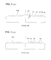
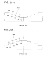
- the diffraction structure there are several kinds of structure are available as shown in Figs. 1 - 4 described below.
- Fig. 1 schematically shows a structure having plural ring zones 100 having a cross section including the optical axis being shaped in a saw tooth.
- Fig. 2 schematically shows a structure having stepping structure 101 including plural zone 102 in an effective aperture having a cross section including an optical axis being shaped in a step shape.
- Fig. 3 schematically shows a structure having plural zone 103 including a stepping structure therein.
- Fig. 1 schematically shows a structure having plural ring zones 100 having a cross section including the optical axis being shaped in a saw tooth.
- Fig. 2 schematically shows a structure having stepping structure 101 including plural zone 102 in an effective aperture having a cross section including an optical axis being shaped in a step shape.
- Fig. 3 schematically shows
- FIG. 4 schematically shows a structure having plural zone 105 including stepping structure 104 in an effective aperture, in which the direction of stepping structure 104 is changed.
- the structure shown in Fig. 4 may be a diffraction structure or a optical path giving structure.
- Figs. 1 -4 schematically shows examples in which each phase structure is formed on a plane surface. However each phase structure may be formed on an aspherical surface.
- an objective optical element is a optical system including at least a beam-condensing element having a function to condense light beams onto each information recording surface of optical discs having different recording density, the objective optical element being provided in an optical pickup apparatus, which is positioned opposed to an optical disc.
- the objective optical system may be structured merely a beam-condensing element.
- the phase structure is formed on the optical surface of the beam-condensing element.
- the optical system structured by the optical element and the beam-condensing element becomes a objective optical element.
- the objective optical element is structured by plural optical elements, a phase structure may be formed in an optical surface of the beam-condensing element. It is preferable that the phase structure is formed on the optical surface of an optical element other than the beam-condensing element in order to decrease the affect of beam eclipse of a stepping portion of the phase structure.
- the beam-condensing element described above may be a plastic lens or a glass lens.
- a plastic material of cyclic olefin is used. It is preferable that among the cyclic olefin, there is used a plastic material having a refractive index N 405 being within a rage of 1.54 - 1.60 at a temperature of 25°C, and a rate of change of the refractive index dN 405 /dT (°C -1 ) of a wavelength 405 nm being -10 x 10 -5 - (- 8) x 10 -5 in temperature range from - 5°C to 70°C.
- the life of die can be prolonged by using glass material having a glass transition temperature Tg of 400°C, since the glass material is deformed at relatively low temperature.
- a glass material having low transition temperature for example, there are K-PG325 and K-PG 375, both are product names of Sumita Optical Glass Corporation.
- the specific gravity of glass is in general larger than that of a plastic lens, if the beam-condensing element is a glass lens, the weight of the objective optical lens becomes heavy and the workload on an actuator to drive the objective optical system becomes heavy. Accordingly, it is preferable that when the beam-condensing element is a glass lens, low specific gravity glass is used. It is preferable that the specific gravity of the glass material is not more than 3.0, preferably not more than 2.8.
- the material of the beam-condensing element material in which particles having a diameter of not more than 30 nm are dispersed may be used.
- the temperature dependency of refractive index can be cancelled by mixing the inorganic material having a characteristic that the refractive index goes up when temperature goes up into plastic material having characteristic that the refractive index goes down when temperature goes up. Consequently, optical material (it will be called athermal plastic hereinafter) having a low rate of change for a refractive index against temperature change can be obtained while maintaining the moldablility of plastic material.
- n denotes a refractive index of the beam-condensing element against a wavelength of a laser beam source
- ⁇ denotes a line expansion coefficient
- [R] denotes a molecular refractive power
- This volume ratio can be adjusted to control the rate of the refractive change against temperature change. Also it is possible to blend and disperse plural kinds of nanometer-sized inorganic.
- ground material 80 and niobium oxide 20 in volume ratio are uniformly mixed.
- the vole ratio can be adjusted between 90 : 10 and 60 : 40. If volume ratio is smaller than 90 : 10, then the effect to suppress the refractive change becomes small and if the volume ratio is over 60 : 40, then the formability of athermal resin becomes problematic.
- the fine particle is inorganic material, and oxide material, which cannot be further oxidized is more preferable. Since inorganic material suppresses reaction against plastic material being polymer organic compound, and oxide prevents the transmission efficiency degradation and wavefront aberration caused by long time irradiation of blue-violet laser. Particularly, a severe condition that blue-violet laser irradiates a beam-condensing element for a long time, oxidation tends to be proceeded. However if the beam-condensing element is formed by inorganic material, the transmission efficiency degradation and the wavefront aberration can be prevented.
- the diameter of fine particle, which is dispersed into plastic material is large, incident light beams tend to be dispersed and the transmission efficiency of a beam-condensing element goes down.
- the transmission efficiency of a beam-condensing element for blue-violet laser is low, it will be a disadvantage from the viewpoint of high speed recording and capability of recording/reproducing information onto/from a multi-layer optical disc, taking account that output power of blue-violet laser used for recording/reproducing information is not high enough. Consequently, it is preferable that the diameter of fine particle dispersed into plastic material is not more than 20 nm, further preferably not more than 10 - 15 nm from the view point of prevention of transmission efficiency of the beam-condensing element.
- an optical pickup apparatus capable of appropriately recording/reproducing information onto/from a high density DVD, a conventional DVD and CD.
- the recording densities ( ⁇ 1 - ⁇ 4) of the first disc - fourth disc are ⁇ 4 ⁇ ⁇ 3 ⁇ ⁇ 2 ⁇ ⁇ 1.
- the magnification factor of objective optical system OBJ1 or OBJ2, when recording/reproducing information onto/from the first optical disc - the fourth optical disc, are the first magnification factor M1 - the fourth magnification factor M4.
- the combination of a wavelength, a thickness of a protective layer, a numerical aperture, a recording density and a magnification factor is not limited to this embodiment.
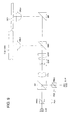
- Fig. 5 shows a sectional schematic drawing of an optical pickup of the first embodiment of the present invention capable of recording/reproducing information onto/from a high density optical disc (the first disc or the second disc), a conventional DVD (the third disc) and a CD (the fourth disc).
- a high density optical disc the first disc or the second disc
- a conventional DVD the third disc
- a CD the fourth disc
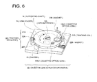
- Fig. 6 shows a bird's view of an objective lens actuator apparatus used for the optical pickup apparatus of the embodiment of the invention.
- the objective lens actuator apparatus will be described.
- Objective lens actuator apparatus 10 shown in Fig. 6 is provided in the optical pickup apparatus shown in Fig. 5.
- the objective lens actuator apparatus 10 comprises OBJ1 (the first objective optical element), OBJ2 (the second objective optical element) condensing laser beams from a semiconductor laser diode onto different information recording surfaces of different optical discs, lens holder 13 for holding objective optical elements OBJ1 and OBJ2 on the same circumference 13A, chassis 15 for supporting lens holder 13 so that lens holder 13 can freely rotate around supporting shaft 14 provided the center of circumference 13A and reciprocally moving along the center axis of the rotation, a focusing actuator (not shown) to reciprocally move lens holder 13 along supporting axis 14 and tracking actuator 20 to give lens holder 13 rotating power to rotate each objective lens OBJ1 and OBJ2 for fixing a position.
- Objective optical element OBJ1 and OBJ2 are provided in a hole formed in lens holder 13 structured in a circular plate, the hole is formed through lens holder 13.
- Objective optical element OBJ1 and OBJ2 are provided in the same distance from the center of lens holder 13.
- Lens holder 13 is connected to the top end of supporting shaft 14, which is provided on chassis 15 in the center of lens holder 13 so that lens holder 13 can freely rotates.
- a focusing actuator (not shown) is provided under supporting shaft 14.
- this focusing actuator comprises an electric magnet solenoid having a permanent magnet provided in a lower end of supporting shaft 14 and a coil provided around the permanent magnet therein.
- the focusing actuator is designed to adjust a focus distance with a fine pitch by adjusting electric current in the coil to reciprocally moving the supporting shaft 14 and lens holder 13 along the supporting shaft 14 (up and down direction in Fig. 6).
- lens holder 13 is designed to freely swing based on the force of tracking actuator on the center of supporting shaft 14 having an axis parallel to an optical axis.
- Tracking actuator comprises a pare of tracking coil 21A and 21B provided in the edge of lens holder 13, each of which is positioned in a symmetry across supporting shaft 14, two pares of magnets 22A, 22B, 23A and 23B provide adjacent the edge of lens holder 13, each of which is positioned in a symmetry across supporting shaft 14 on chassis 15.
- Positions of magnet 22A and 22B is arranged so that when tracking coils 21A and 21B opposes to a paired magnets 22A and 22B, objective optical element OBJ1 is positioned on the optical path of laser beams and positions of magnet 23A and 23B is arranged so that when tracking coils 21A and 21B opposes to a pared magnets 23A and 23B, objective optical element OBJ2 is positioned on the optical path of laser beams.
- a stopper (not shown) to limit a swinging range is provided in the lens holder 13 so that tracking coils 21A and 21B do not oppose to magnets 22B or 23B, and magnets 22A or 23A respectively.
- Tracking actuator 20 is arranged so that the tangent line direction of outer circumference of lens holder 13 formed in circular shape crosses with the tangential line direction of a track of the optical disc in a right angle. Tracking actuator corrects a deviation of an irradiating position of laser beams to the track by forcing lens holder 13 to swing with a fine pitch. Accordingly, it is necessary that tracking coils 21A and 21B swing lens holder 13 with a fine pitch while tracking coils 21A and 21B respectively oppose to magnets 22A and 22B.
- respective tracking coils 21A and 21B have a piece of iron therein.
- An operation control circuit is designed to control electric current in each tracking coil 21A and 21B so that tacking coils 21A and 21B generate repulsive force against the each magnet while the each magnet pulls the piece of iron.
- optical pickup apparatus of the invention will be described blow.
- lens holder 13 of objective lens actuator 10 is rotated to move objective optical lenses OBJ1 or OBJ2 in a optical path as shown in Fig. 5.
- the first semiconductor laser diode LD1 and the second semiconductor laser diode LD2 are placed on the same printed circuit board, which configures a single unit called two laser diodes in one package.
- the laser beams are shaped in parallel laser beams by collimator lens COL after passing through dichroic prism DP and then pass through polarization beam splitter PBS. And the laser beams are guided to beam expander EXP having optical elements L1 and L2.
- a diffraction structure is provided on the surface of the other optical element L2 to correct chromatic aberration of the laser beams emitted from the first laser diode LD1.
- the diffraction structure for correcting chromatic aberration may be provided not only in optical element L2 but also in other optical elements, for example, collimator lens COL, etc.
- a chromatic aberration correcting function can be achieved not only by the diffraction structure but also by a phase structure and/or multi-level, etc.
- the chromatic aberration and the spherical aberration can be corrected by providing beam expander EXP. Further, when a high density DVD has two information recording surfaces therein, selection of the information recording surface can be conducted by moving optical element L1 in an optical axis direction.
- a chromatic aberration correction optical element and a spherical aberration correction optical element can be provided not only in beam expander EXP but also in objective optical element OBJ1 or OBJ2.
- laser beams passed through beam expander EXP pass through quarter wave plate QWP and diaphragm AP guided to objective optical elements OBJ1 or OBJ2 which is formed by merely a refraction surface.
- Laser beams reflected by an information pit on an information recording surface again pass through objective optical elements OBJ1 or OBJ2, diaphragm AP, quarter wave plate QWP and beam expander EXP. Then the laser beams are reflected by polarized beam splitter PBS and cylindrical lens CY1 gives astigmatism to the laser beams. Then the laser beams reach to photo-detector PD after passing through sensor lens SL1. Information recorded on the first optical disc OD1 or the second optical disc OD2 is obtained by using the output of photo-detector PD.
- Focal point detection and track detection are performed by detecting the change of laser beam amount based on the change of a laser beam spot shape and the change of a laser beam spot location. Based on these detections, a focusing actuator (not shown) and tracking actuator 20 of objective lens actuator mechanism 10 moves objective optical element OBJ1 or objective optical element OBJ2 so that laser beams from the first laser diode LD1 are condensed on the information recording surface of the first optical disc OD1 or the second optical disc OD2.
- the laser beams pass through dichroic prism DP and are shaped into parallel laser beams by collimator lens. Then the laser beams pass through polarized beam splitter PBS and enter into beam expander EXP having optical elements L1 and L2.
- laser beams passed through beam expander EXP pass through quarter wave plate QWP and diaphragm AP guided to objective optical elements OBJ1 or OBJ2 which is formed by merely a refraction surface.
- Laser beams reflected by an information pit on an information recording surface again pass through objective optical elements OBJ1 or OBJ2, diaphragm AP, quarter wave plate QWP and beam expander EXP. Then the laser beams are reflected by polarized beam splitter PBS and cylindrical lens CY1 gives astigmatism to the laser beams. Then the laser beams reach to photo-detector PD after passing through sensor lens SL1. Information recorded on the third optical disc OD3 is obtained by using the output of photo-detector PD.
- Focal point detection and track detection are performed by detecting the change of laser beam amount based on the change of a laser beam spot shape and the change of a laser beam spot location. Based on this detection, a focusing actuator (not shown) and tracking actuator 20 of objective lens actuator mechanism 10 moves objective optical element OBJ1 or objective optical element OBJ2 so that laser beams from the second laser diode LD2 are condensed on the information recording surface of the third optical disc OD3.
- the laser beams pass through dichroic prism DP and are shaped into parallel laser beams by collimator lens. Then the laser beams pass through polarized beam splitter PBS and enter into beam expander EXP having optical elements L1 and L2.
- laser beams passed through beam expander EXP pass through quarter wave plate QWP and diaphragm AP guided to objective optical elements OBJ1 or OBJ2 which is formed by merely a refraction surface.
- Laser beams reflected by an information pit on an information recording surface again pass through objective optical elements OBJ1 or OBJ2, diaphragm AP, quarter wave plate QWP and beam expander EXP. Then the laser beams are reflected by polarized beam splitter PBS and cylindrical lens CY1 gives astigmatism to the laser beams. Then the laser beams reach to photo-detector PD after passing through sensor lens SL1. Information recorded on the forth optical disc OD4 is obtained by using the output of photo-detector PD.
- Focal point detection and track detection are performed by detecting the change of laser beam amount based on the change of a laser beam spot shape and the change of a laser beam spot location. Based on this detection, a focusing actuator (not shown) and tracking actuator 20 of objective lens actuator mechanism 10 moves objective optical element OBJ1 or objective optical element OBJ2 so that laser beams from the third laser diode LD3 are condensed on the information recording surface of the fourth optical disc OD4.
- Fig. 7 shows a schematic diagram of an optical pickup apparatus of a second embodiment of the present invention.
- the first, second and third semiconductor laser diodes are attached on the same board, which is a single unit called three laser diodes in one package 3LIP.
- a beam shape of laser beams emitted from the first semiconductor laser diode LD1, the second semiconductor laser diode LD2 and the third semiconductor laser diode LD3 is corrected by beam shaper BS.
- the laser beams are shaped in parallel laser beams by collimator lens COL and then pass through polarization beam splitter PBS. And the laser beams are guided to beam expander EXP having optical elements L1 and L2.
- Laser beams passed through beam expander EXP pass through quarter wave plate QWP and diaphragm AP guided to objective optical elements OBJ1 or OBJ2 which is formed by merely a refraction surface.
- the laser beams pass through objective optical elements OBJ1 or OBJ2 is collected into a focal spot on an information recording surface of any one of the first - fourth optical discs OC1 - OD4 through the protective layer.
- Laser beams reflected by an information pit on an information recording surface again pass through objective optical elements OBJ1 or OBJ2, diaphragm AP, quarter wave plate QWP and beam expander EXP. Then the laser beams are reflected by polarized beam splitter PBS and cylindrical lens CY1 gives astigmatism to the laser beams. Then the laser beams reach to photo-detector PD after passing through sensor lens SL1. Information recorded on any one of the first, second, or fourth optical disc OD1, OD2, OD3 or OD4 is obtained by using the output of photo-detector PD.
- Focal point detection and track detection are performed by detecting the change of laser beam amount based on the change of a laser beam spot shape and the change of a laser beam spot location. Based on this detection, a focusing actuator (not shown) and tracking actuator 20 of objective lens actuator mechanism 10 moves objective optical element OBJ1 or objective optical element OBJ2 so that laser beams from the third laser diode LD3 are condensed on the information recording surface of any one of the first, second, or fourth optical disc OD1, OD2, OD3 or OD4.
- either of objective optical lenses is mechanically placed in an optical path by moving lens holder 13 on which two objective optical lenses BJ1 and OBJ2 are fixed.
- the first variation has a moving mirror or a movable prism to change an optical path to either of the objective optical elements corresponding to the optical disc to be used while objective optical elements OBJ1 and OBJ2 are fixed.
- "Fixed" in the above sentence means that Objective optical elements OBJ1 and OBJ2 moves in the optical axis direction for focusing, however they do not move in the direction being vertical to the optical axis.
- Another variation is that a polarized beam splitter, etc.
- objective optical elements OBJ1 and OBJ2 are respective different bodies.
- objective elements OBJ1 and OBJ2 are formed in a body in a parallel arrangement.
- Figs. 9 and 10 show pickup apparatus configurations in which the positions of objective optical elements described above are fixedly deployed.
- Fig. 9 shows a configuration for recording and or reproducing information onto or from each disc by separating an optical path using half mirror HMR as a beam splitter and guiding optical beams into objective optical elements OBJ3 and OBJ4 which are fixedly deployed so that each optical axis is arranged to be parallel each other.
- Fig. 10 shows a configuration for recording and or reproducing information onto or from each disc by a movable mirror which moves between the first position where light beams are guided to objective optical element OBJ3 instead of half mirror HMR as a beam splitter shown in Fig. 9 and a second position where light beams are guided to objective optical element OBJ4.
- Other configurations are the same as configurations shown in Fig. 9.
- semiconductor laser L1 as a first light source for BD or HD
- semiconductor laser L2 as a second light source for DVD
- semiconductor laser L3 as a third light source for CD, which are packaged into one package 2L1F in this embodiment.
- the light beams passed through beam expander EXP transmit through quarter wave plate QWP (and aperture AP). A part of the light beams reflected by half mirror HMR and the other pass through half mirror HMR.
- Half mirror HMR is arranged to separate almost all incident light beams having wavelength of ⁇ 1 into transmitted light beams and reflected light beams, and to transmit or reflect almost all the incident light beams having wavelength ⁇ 2 and ⁇ 3.
- the configuration shown in Fig. 9 is an example of reflection.
- half mirror When recording and or reproducing information onto or from the first optical disc OD1, half mirror reflects a part of light beams transmitted through the half mirror to change the direction of the light beams for guiding the light beams into optical objective element OBJ4.
- the reflected light beams modulated and reflected by information pits on the information recording surface are guided into photo-detector PD1 after passing back through objective optical element OBJ3 or OBJ4, half mirror HMR, quarter wave plate QWP and beam expander EXP, and reflected by polarized beam splitter PBS1. Since the light beams enters into photo detector PD1, information signals which are recorded onto the first optical disc OD1 and second optical disc OD2 are obtained by using the output signal of photo-detector PD1. Focal point detection and tacking detection are performed by detecting a light beam amount change caused by a shape change and position change of the spot formed on the photo detector PD.
- a focusing actuator and a tracking actuator (not shown) of an objective lens actuator mechanism moves objective optical elements OBJ3 or OBJ4 as one body so that the light beams emitted from the first semiconductor laser LD1 is focused onto the information recording surface of the first optical disc OD1 and the second optical disc OD2.
- the light beams modulated and reflected by information pits on the information recording surface are guided into photo-detector PD2 after passing back through objective optical element OBJ3, half mirror HMR, quarter wave plate QWP, beam expander EXP and collimator COL, then reflected by dichroic prism DP and polarized beam splitter PBS2.
- Information signal, which is recorded onto the third optical disc OD3 is obtained by using the output signal of photo-detector PD 2.
- Focal point detection and tacking detection are performed by detecting a light beam amount change caused by a shape change and position change of the spot formed on the photo detector.
- a focusing actuator and a tracking actuator (not shown) of an objective lens actuator mechanism moves objective optical elements OBJ3 as one body so that the light beams emitted from the second semiconductor laser LD2 is focused onto the information recording surface of the third optical disc OD3.
- the reflected light beams modulated and reflected by information pits on the information recording surface are guided into photo-detector PD2 after passing back through objective optical element OBJ3, half mirror HMR, quarter wave plate QWP, beam expander EXP and collimator COL, then reflected by dichroic prism DP and polarized beam splitter PBS2.
- Information signal, which is recorded onto the fourth optical disc OD4 is obtained by using the output signal of photo-detector PD 2.
- Focal point detection and tacking detection are performed by detecting a light beam amount change caused by a shape change and position change of the spot formed on the photo detector.
- a focusing actuator and a tracking actuator (not shown) of an objective lens actuator mechanism moves objective optical elements OBJ3 as one body so that the light beams emitted from the third semiconductor laser LD3 is focused onto the information recording surface of the fourth optical disc OD4.
- Dichroic prism DP has a characteristic to transmits light beams having wavelength ⁇ 1 and reflects light beams having wavelength ⁇ 2 and ⁇ 3.
- beam expander EXP comprises plural optical elements and at least one optical element moves in an optical axis direction so as to change (here enlarge) an optical beam diameter of parallel beams from collimator COL.
- beam expander EXP may have functions to correct chromatic aberration and spherical aberration as other functions.
- Chromatic aberration here is aberration caused by wavelength drift and spherical aberration is one of aberration of spherical aberration caused by the differences between the thickness of protective layer of respective optical discs, spherical aberration caused by wavelength drift, and spherical aberration caused by temperature drift.
- the beam expander having plural optical elements may perform these aberration corrections.
- the step difference structure includes a diffraction structure for decreasing aberration by causing diffraction action in incident light beams, a phase structure for decreasing aberration by causing phase difference, both structures on different optical surfaces, a step difference structure superimposing the diffraction structure and the phase structure on a same optical surface and a step difference structure including small steps therein having a wavelength selectivity.
- beam expander EXP comprises plural optical element. However, it may be a single optical element.
- the step difference structure may be provided not only on beam expander EXP but also other optical elements, such as collimator COL, etc., or objective optical element OBJ3 (OBJ4).
- other optical elements such as collimator COL, etc., or objective optical element OBJ3 (OBJ4).
- Chromatic aberration and spherical aberration can be corrected by providing the beam expander EXP described above. Further, it becomes possible to select the information recording surface by moving optical element in light beam side when high density DVD has dual layers of information recording surfaces.
- PD1 and PD2 are separately provided. However, these photo detectors may be integrated into one sensor, which can be commonly used for from the first to the third light beams. If this is the case, it is easily understand that PD2 and PDS2 which are shown in Figs. 9 and 10, become unnecessary.
- collimator COL which is commonly used for these wavelengths.
- this collimator COL can be a collimator for two wavelengths for BD and for DVD/CD.
- a half mirror is used to change the direction of light beams to guide them to objective optical elements OBJ3 and OBJ4.
- This structure is preferable to decrease the number of optical systems, however the structure is not limited to this structure.
- the beams splitter used here may be an optical element having a structure to polarize light beams to plural directions, which is capable of guiding incident light beams to each optical element.
- the beam splitter is not limited to a half mirror which selectively transmits or reflects incident light beams.
- it may be a structure for separating light beams into a first polarized direction element of incident light beams and a second polarized direction element of different polarized direction element for the first polarized direction element, which is the same as a polarized beam splitter.
- PBS1 is not necessary to be a half mirror.
- Fig. 10 illustrates a configuration having two lens system including mirror MR for moving to guide blue-violet laser beams to objective optical element OBJ3 for HD/DVD/CD and to objective optical element OBJ4 for BD, which is the same as Fig. 9.
- NA1 0.85 - 0.9
- NA2 0.65 -0.67
- NA3 0.60 - 0.67
- NA4 0.45 - 0.53.
- HWL is a blaze wavelength of a grating. Power of 10, for example, 2.5 x 10 - 3 , will be expressed in 2.5 E - 3, hereinafter.
- the optical surface of the objective optical system is formed on an aspheric surface which is defined by formula (2) below when substituting the coefficients shown in Table 1.
- X (h) denotes an axis in the optical axis (a laser beam traveling direction is defined as positive direction); K denotes a constant of cone; A 2 denotes aspheric constant; and h denotes a height from the optical axis.
- Optical path length given to laser beams of each wavelength by the diffraction structure is defined as following formula with substituted coefficient shown in Table 1.
- B 21 is a coefficient of an optical path difference function.
- the first objective optical element is used to record/reproduce onto/from HD (the second optical disc) and DVD(the third optical disc) and the second objective optical element is used to record/reproduce onto/from BD (the first optical disc) and CD (the fourth optical disc).
- Embodiments 1 - 6 of the first objective optical lens in embodiment A will be described. (Embodiments 1 - 4)
- the first objective optical element is structured by a single plastic lens L1.
- Plural ring zones being diffraction structures DOE shown in Fig. 1 are arranged on light source side surface S1, centering on an optical axis, each zone being formed in a sawtooth (it will be called diffraction structure DOE hereinafter) in a light source side on the single plastic lens L1.
- Disc side surface S2 of single plastic lens L1 is an aspherical surface.
- Embodiment 1 second order first order Embodiment 2 third order second order Embodiment 3 fifth order third order Embodiment 4 eighth order fifth order
- Single lens L1 has refractive index nd of 1.5435, and abbe constant vd of 56.7, measured by D-line.
- Lens data of each embodiment is shown in Tables 2 - 5.
- NA 2 optical surface S1 of single lens L1 is structured in a single area.
- NA2 area can be divided into first area AREA 1 corresponding to the NA2 area of the first laser beams including an optical axis and second area AREA 2 which is an area from NA2 of the first laser beams and NA2 of the second laser beams, each area may has a different phase structure.
- Diffraction structure DOE is a structure to secure compatibility for recording/reproducing information onto/from respective optical discs corresponding to the first laser beams having wavelength ⁇ 1 and the second laser beams having wavelength ⁇ 2.
- Diffraction structure DOE is also a structure to suppress chromatic aberration of an objective optical lens in blue-violet range and a spherical aberration change due to a temperature change, which are to be problems when single lens L1 is formed by a plastic lens.
- height "d" of a step being the nearest to the optical axis is designed so that the diffraction efficiency of required order of diffraction beams for wavelength 400 nm - 420 nm becomes 100%.
- the height of step of a diffraction structure is designed so that when laser beams having wavelength of 400 nm enter into the diffraction structure, the diffraction efficiency of the second order diffraction beams becomes 100%, the allocation of the diffraction efficiency is possible so that plus second diffraction beams occur at about 97% diffraction efficiency when the first beams enter into the structure, and plus first diffraction beams occur at about 94% diffraction efficiency when the second beams enter into the structure.
- the same allocation of diffraction efficiency for the pair of other diffraction orders is possible and practically enough diffraction efficiency can be obtained. It is also possible to put more importance on the second light beam diffraction efficiency by optimizing the diffraction efficiency for the first wavelength of ⁇ 1.
- diffraction structure DOE has characteristics that when the wavelength of incident light beams become longer, the spherical aberration changes to an under correction direction and when the wavelength become shorter, the spherical aberration changes to a correction direction. Consequently, it is possible to expand the temperature range by canceling spherical aberration changes caused in a condensing element due to environmental temperature changes.
- diffraction structure DOE is provided on optical surface S1, however it is possible to provide diffraction structure DOE on optical surface S2.
- the first objective optical element is structured by a single plastic lens L1 and both surfaces, light source side surface S1 and optical disc side S2 are aspherical surfaces.
- the first objective optical lens will be described in detail below.
- Single lens L1 has refractive index nd of 1.5435, and abbe constant vd of 56.7, which are measured by D-line.
- Lens data of each embodiment 5 is shown in Tables 6.
- the first objective optical element is structured by single plastic lens L1. Since NA for both optical discs are the same, which is NA 2, optical surface S1 of single lens L1 being a light source side, is structured in a single area.
- Optical disc side surface S2 of single lens L1 is aspherical surface.
- Single lens L1 has refractive index nd of 1.5435, and abbe constant vd of 56.7, measured by D-line.
- Lens data of each embodiment is shown in Tables 7. S1 Surface diffraction Order 405nm 655nm Zero Order First Order
- Optical surface S1 of a laser source side of a semiconductor laser diode has a structure having diffraction structure HOE having plural zone forming a stepping structure, which is provided centering on an optical axis as shown in Figs 3(c) and 3(d).
- the depth of a stepping structure D is set by a value calculated by following formula (2).
- D x (N1 - 1) / ⁇ 1 2 x q
- Dividing number P being a number of steps in each ring zone is set to 5.
- diffraction structure HOE is provided on optical surface S1 of single lens L1 in a semiconductor laser source side surface S1, however diffraction structure HOE may be provided on optical disc side surface S2.
- the second objective optical element is structured by a single plastic lens L1.
- Light source side surface S1 is divided into first area AREA1 including an optical axis corresponding to an area in NA3 and second area AREA2 corresponding to an area from NA3 to NA1.
- First area AREAL has plural ring zones centering on the optical axis, which have a sawtooth shaped diffraction structure (it will be called "diffraction structure DOE" hereinafter) as shown in Fig. 1.
- Second area AREA2 has a different structure of aspherical surface from an aspherical surface of a base structure of first area AREA1.
- Optical disc side surface S2 of singe lens L1 has an aspherical surface.
- Single lens L1 has refractive index nd of 1.5435, and abbe constant vd of 56.7, measured by D-line.
- Lens data of each embodiment is shown in Tables 8. Diffraction Order 405nm 785nm
- Second area AREA2 of semiconductor laser beam source side of single lens L1 does not have a phase structure, however a phase structure different from the phase structure of first area RRER1 may be provide in second area AREA2.
- Diffraction structure DOE is a structure to secure compatibility for recording/reproducing information onto/from an optical disc for the first laser beams having wavelength ⁇ 1 and the third laser beams having wavelength ⁇ 3.
- Diffraction structure DOE is also a structure to suppress chromatic aberration of an objective optical lens in blue-violet range and a spherical aberration change due to a temperature change, which are to be problems when single lens L1 is formed by a plastic lens.
- height "d1" of a step being the nearest to the optical axis is designed so that the diffraction efficiency of required order of diffraction beams for wavelength 400 nm - 420 nm becomes 100%.
- the height of step of a diffraction structure is designed so that when laser beams having wavelength of 400 nm enter into the diffraction structure, the diffraction efficiency of the second order diffraction beams becomes 100%, the allocation of the diffraction efficiency is possible so that plus second diffraction beams occur at about 97% diffraction efficiency when the first beams enter into the structure, and plus first diffraction beams occur at about 94% diffraction efficiency when the second beams enter into the structure.
- the same allocation of diffraction efficiency for the pair of other diffraction orders is possible and practically enough diffraction efficiency can be obtained. It is also possible to put more weight on the second light beam diffraction efficiency by optimizing the diffraction efficiency for the first wavelength of ⁇ 1.
- the third light beams passed through diffraction structure DOE and a protective layer of CD form a appropriate light beam spot on a recording surface of a CD by canceling spherical aberration in an over-correction direction caused by the difference between the thickness of a BD protective layer and the thickness of a CD protective layer.
- diffraction structure DOE is provided on optical surface S1, however diffraction structure S2 may be provided in optical surface S2.
- the second objective optical element comprises plastic lens L1 and glass lens L2.
- Diffraction structure HOE having a structure on which plural ring zones are provided centering on the optical axis plastic lens L1 as shown in Figs. 3(c) and 3(d) on disc side surface S2 of plastic lens L1.
- the zone structure corrects the aberration caused by the wavelength difference or the temperature difference described above.
- the base surface shape of optical surface S1 is a flat and the base surface shape of optical surface S2 is a concave spherical surface.
- the bases surface may be a surface other than a plain surface or a spherical surface. For example, by making the base surface into a aspherical surface, it increases the degree of freedom to correct out of out-of-axis aberration and to control higher order aberration etc.
- Lens L2 is a dual-face aspherical lens of structured by a glass mold and designed so that the spherical aberration determined by the combination with a finite magnification factor determined by a concave surface and a BD protective layer becomes the minimum value.
- first magnification factor M1 for the first light beams and the fourth magnification factor M4 for the third light beam becomes an over correction direction without the phase structure.
- setting a magnification factor for the third light beams to a finite magnification factor cancels and corrects spherical aberration, which is in a state of a over correction direction, caused by the difference between the thickness of a BD protective layer and the thickness of a CD protective layer.
- Lens L1 is a plastic lens having refractive index nd of 1.54087, and abbe constant vd of 56.3, measured by D-line.
- Lens L2 is a glass mold lens having refractive index nd of 1.61544, and abbe constant vd of 60.0, measured by D-line. Data of each embodiment is shown in Tables 9.
- lens L1 and lens L2 When combining lens L1 and lens L2 into a single body, it is natural that a separated lens barrel is used to support a lens. However, it is possible to have a structure having a flange on the circumference of the optical functional portion of lens L1, (through which the first light beams pass) and connecting the flange with lens L2 to combine them into one body by welding or adhering.
- Optical surface S2 of lens L1 is divided first area AREA3 including an optical axis corresponding to an area of NA3 and second area AREA4 corresponding from NA3 to NA1 as shown in Fig. 8(C).
- First area AREA3 has a structure having diffraction structure HOE having plural zone forming a stepping structure, which is provided centering on an optical axis as shown in Figs 3(c) and 3(d).
- the depth of a stepping structure D ( ⁇ m) is set by a value calculated by following formula (3).
- D x (N1 - 1) / ⁇ 1 1 x q
- Dividing number P being a number of steps in each zone is set to 2.
- the dividing number P is set to 2
- the third laser beams are diffracted in the plus/minus first order direction (plus first order diffraction beams and minus first order diffraction beams). At that time, the diffraction efficiency of the plus first order diffraction beams of the second laser beams is a little over 40 %, and minus first order diffraction light beams become flare.
- Optical surface S2 of lens L1 is divided into first area AREAL including an optical axis corresponding to an area of NA3 and second area AREA2 corresponding to from NA3 to NA4 as shown in Fig. 8. It becomes possible to increase a degree of design freedom by incorporating plural zone having different phase functions therewith, which is provided centering on an optical axis.
- Each zone width of diffraction structure HOE provided on optical surface S2 located in an optical disc side of lens L1 is designed to add spherical aberration in an under correction direction against plus first order diffraction light beams based on diffraction action.
- the third light beams passed through diffraction structure DOE and a protective layer of CD form a appropriate light beam spot on a recording surface of CD by canceling spherical aberration in an over-correction direction caused by the difference between the thickness of a BD protective layer and the thickness of a CD protective layer.
- diffraction structure HOE is provided on lens L1, however diffraction structure HOE may be provided on lens L2.
- a diffraction structure having plural zone shaped in a sawtooth shape in a cross section including an optical axis may be formed in first area AREA1 and second area AREA2 in semiconductor laser beam source side and optical surface S2 in an optical disc side.
- the diffraction structure DOE is a structure to suppress chromatic aberration of an objective optical element.
- height "d1" of a step being the nearest to the optical axis is designed so that the diffraction efficiency of required order of diffraction beams for wavelength 400 nm - 420 nm becomes 100%.
- DOE 1 in which the depth of the step is set as described above, diffraction beams occurs with diffraction efficiency of not less than 95%, which is highly enough diffraction efficiency, and it becomes possible to correct chromatic aberration in a blue-violet range.
- the second objective optical lens of the embodiment of the invention does not have diffraction structure DOE, however diffraction structure DOE may be provided on an optical surface of lens L2.
- Diffraction structure DOE may be a structure, which is provided on an entire optical surface of lens L2 as a one area or an optical surface of lens L2 having diffraction structure DOE thereon may be divided into two areas centering on the optical axis, each of which has a different diffraction structure DOE each other.
- the diffraction efficiency of the each area, where the first light beams and the third light beams passes through, may be arranged to be balanced. Or a structure on which the importance of the diffraction efficiency for the first light beams is attached by optimizing the efficiency against the first wavelength ⁇ 1.
- diffraction structure HOE is provided on optical surface S2 of an optical disc.
- diffraction structure HOE may be provide on optical surface S1.
- the first objective optical element is used for HD (the second optical disc) and CD (the fourth optical disc), and the second objective optical element is used for BD (the first optical disc) and DVD (the third optical disc).
- Embodiments 1 - 4 of the first objective optical lens in embodiment B will be described. (Embodiment 1 - 4)
- the first objective optical element is structured by a single plastic lens L1.
- Plural ring zones being diffraction structures DOE as shown in Fig. 1 are arranged on light source side surface S1, centering on an optical axis, each zone being formed in a sawtooth (it will be called diffraction structure DOE hereinafter) in a light source side on the single plastic lens L1.
- Disc side surface S2 of single plastic lens L1 is an aspherical surface.
- Single lens L1 has refractive index nd of 1.5435, and abbe constant vd of 56.7, measured by D-line.
- Lens data of embodiment 2 is shown in Tables 11. S1 Surface Diffraction Order 405nm 785nm Second Order First Order S1 Surface Diffraction Order 405nm 785nm Second Order First Order
- Optical surface S1 of single lens L1 in a semiconductor laser diode side is configured by a single area.
- optical surface S1 may be divided into first area AREA1 corresponding to an area in NA3 including an optical axis of single lens L1 and second area AREA2 corresponding for NA3 to NA2, each area having a different phase structure from each other.
- Diffraction structure DOE is a structure to secure compatibility for recording/reproducing information onto/from an optical disc for the first laser beams having wavelength ⁇ 1 and the third laser beams having wavelength ⁇ 3.
- Diffraction structure DOE is also a structure to suppress chromatic aberration of an objective optical lens in blue-violet range and a spherical aberration change due to a temperature change, which are to be problems when single lens L1 is formed by a plastic lens.
- height "d" of a step being the nearest to the optical axis is designed so that the diffraction efficiency of required order of diffraction beams for wavelength 400 nm - 420 nm becomes 100%.
- the height of step of a diffraction structure is designed so that when laser beams having wavelength of 400 nm enter into the diffraction structure, the diffraction efficiency of the second order diffraction beams becomes 100%, the allocation of the diffraction efficiency is possible so that plus second diffraction beams occur at about 97% diffraction efficiency when the first beams enter into the structure, and plus first diffraction beams occur at about 94% diffraction efficiency when the second beams enter into the structure. It is also possible to put more importance on the second light beam diffraction efficiency by optimizing the diffraction efficiency for the first wavelength of ⁇ 1.
- diffraction structure DOE has characteristics that when the wavelength of incident light beams become longer, the spherical aberration changes to an under correction direction and when the wavelength become shorter, the spherical aberration changes to a correction direction. Consequently, it is possible to expand the temperature range by canceling spherical aberration changes caused in a condensing element due to environmental temperature changes.
- Each zone width of diffraction structure HOE provided on optical surface S2 located in an optical disc side of lens L1 is designed to add spherical aberration in an under correction direction against plus first order diffraction light beams based on diffraction action.
- the third light beams passed through diffraction structure DOE and a protective layer of CD form a appropriate light beam spot on a recording surface of a CD by canceling spherical aberration in an over-correction direction caused by the difference between the thickness of a BD protective layer and the thickness of a CD protective layer.
- diffraction structure HOE is provided on optical surface S1, however diffraction structure HOE may be provided on optical surface S2.
- the first objective optical element is configured by a plastic single lens L1, whose optical source side surface S1 and optical disc side surface S2 are aspherical surfaces.
- Single lens L1 is a plastic lens having refractive index nd of 1.5435, and abbe constant vd of 56.7, measured by D-line.
- Lens L2 is a glass mold lens having refractive index nd of 1.5372.
- Lens data of embodiment 3 is shown in Tables 12.
- setting a magnification factor for the third light beams to a finite magnification factor cancels and corrects spherical aberration being in a over correction direction caused by the difference between the thickness of a HD protective layer and the thickness of a CD protective layer.
- the first objective optical element is structured by a single plastic lens L1.
- Light source side optical surface S1 is divided into first area AREA1 including an optical axis corresponding to an area in NA3 and second area AREA2 corresponding to an area from NA3 to NA2.
- First area AREA1 has plural ring zones centering on the optical axis, which have a sawtooth shaped diffraction structure HOE as shown in Figs. 3(c) and 3(d).
- Second area AREA2 of semiconductor laser diode side optical surface S1 is a flat surface and another phase structure may be provided therein.
- Single lens L1 has refractive index nd of 1.5435, and abbe constant vd of 56.7, measured by D-line.
- Lens data of each embodiment is shown in Tables 13. S1 Surface Diffraction Order 405nm 785nm Zero Order First Order
- Optical surface S1 in semiconductor laser diode side of single lens L1 may be divided into first area AREA1 corresponding to an area in NA3 including an optical axis of single lens L1 and second area AREA2 corresponding to from NA3 to NA2.
- Diffraction structure HOE having plural zone in which a stepping structure is arranged centering on optical axis is provided in first area AREA1.
- the depth of stepping structure D is set by a value calculated by following formula (4).
- D x (N1 - 1) / ⁇ 1 2 x q
- Dividing number P being a number of stepping structure in each zone is set to 2.
- the dividing number P is set to 2
- the third laser beams are diffracted in the plus/minus first order direction (plus first diffraction beams and - first diffraction beams). At that time, the diffraction efficiency of the plus first diffraction beams of the second laser beams is a little over 40 %, and minus first order diffraction light beams become flare.
- Embodiments of 1 and 2 of the second objective optical element which can be combined with the first objective optical element in embodiment B will be described below.
- the second objective optical element has two plastic lenses, which are lens L1 and lens L2 from a light beam source side.
- Lens L1 has a diffraction type phase structure on both surfaces.
- a zone structure shown in Figs. 2 and 4 is provided on optical disc side surface S2 of lens L1.
- the zone structure corrects the aberration caused by the wavelength difference or the temperature difference described above.
- the base surface shape of optical surface S1 is a flat and the base surface shape of optical surface S2 is a concave spherical surface.
- the bases surface may be a surface other than a plain surface or a spherical surface. For example, by making the base surface into a aspherical surface, it increases the degree of freedom to correct out of out-of-axis aberration and to control higher order aberration etc.
- Lens L2 is a plastic lens having refractive index nd of 1.5435 measured by D-line and abbe constant vd of 56.7.
- a flange formed together with each optical functional portion of respective areas of lens L1 and lens L2, through which the first light beams pass, is provided around the optical functional portion. A portion of the flange connects both lens L1 and lens L2 into one body. When combining lens L1 and lens L2 into one body, a lens barrel may be used.
- the lens data of lenses used in embodiment 1 is shown in Table 14. Diffraction Order 405nm 655nm S1 Zero Order First Order S2 Zero Order Zero Order
- Optical surface S1 in a semiconductor laser diode side of lens L1 is divided first area AREA1 including an optical axis corresponding to an internal area of NA2 and second area AREA2 corresponding from NA2 to NA1 as shown in Fig. 8.
- First area AREA1 has a structure having diffraction structure HOE1 having plural zone forming a stepping structure, which is provided centering on an optical axis as shown in Figs 3(c) and 3 (d) .
- a stepping structure D1 ( ⁇ m) is set by a value calculated by following formula (5).
- D1 x (N1 - 1) / ⁇ 1 2 x q
- Dividing number P being a number of steps in each zone is set to 5.
- Depth D2 ( ⁇ m) of each step between ring zones which are provided in an aspherical surface of one area corresponding to the optical surface S2 in an optical disc side of lens L1 is set by following formula.
- D2 x (N1 - 1) / ⁇ 1 5
- optical path difference of (5 x ⁇ 1 / (N1 - 1) x (N2 - 1) / ⁇ 2) x ⁇ 2 ( ⁇ m) is generated between adjacent ring zones.
- N2 denotes a medium refractive index of lens L1 for wavelength ⁇ 2.
- the optical path difference between adjacent stepping structure is about 3 x ⁇ 2 ( ⁇ m).
- the second light beams pass though the stepping structure as zero-order diffraction light beams without diffraction.
- Optical surface S2 of lens L1 may be divided into third area AREA3 including an optical axis corresponding to an area of NA2 and fourth area AREA4 corresponding to from NA2 to NA1 as shown in Fig. 8(C). It becomes possible to increase a degree of design freedom by incorporating plural zone having different phase functions therewith, which is provided centering on an optical axis.
- the second objective optical element comprises a combination of lens L1 having no phase structure and lens L2.
- first magnification factor M1 for the first light beams and fourth magnification factor M4 for the third light beams to 0 (zero)
- the spherical aberration becomes a state of a over correction direction without a phase structure due to the spherical aberration caused by the difference between the thickness of a BD protective layer and the thickness of a DVD protective layer.
- Each zone width of diffraction structure HOE1 provided on optical surface S1 located in a semiconductor laser light source side of lens L1 is designed to add spherical aberration in an under correction direction against plus first order diffraction light beams based on diffraction action.
- the second light beams passed through diffraction structure HOE1 and a protective layer of BD forms a appropriate light beam spot on a recording surface of a DVD by canceling spherical aberration in an over-correction direction caused by the difference between the thickness of a BD protective layer and the thickness of a DVD protective layer.
- diffraction structure HOE is provided with lens L1, however diffraction structure HOE may be provided with lens L2.
- diffraction structure DOE having plural zone shaped in a sawtooth shape in a cross section including an optical axis may be formed on semiconductor laser beam source side optical surface S1 in second area AREA2 or in an optical disc side optical surface S2.
- the diffraction structure DOE is a structure to suppress chromatic aberration of an objective optical element, which is a problem particularly when lens L2 is structured by a plastic lens, and drift of spherical aberration due to the temperature change.
- height "d1" of a step being the nearest to the optical axis is designed so that the diffraction efficiency of required order of diffraction beams for wavelength 400 nm - 420 nm becomes 100%.
- DOE 1 in which the depth of the step is set as described above, diffraction beams occurs with diffraction efficiency of not less than 95%, which is highly enough diffraction efficiency, and it becomes possible to correct chromatic aberration in a blue-violet range.
- the second objective optical lens of the embodiment of the invention does not have diffraction structure DOE, however diffraction structure DOE may be provided on an optical surface of lens L2.
- Diffraction structure DOE may be a structure, which is provided on an entire optical surface of lens L2 as a one area or an optical surface of lens L2 having diffraction structure DOE thereon may be divided into two areas centering on the optical axis, each of which has a different diffraction structure DOE each other.
- the diffraction efficiency of the each area, where the first light beams and the second light beams passes through, may be arranged to be balanced.
- the height of the step is designed so that the diffraction efficiency becomes 100, (where a refractive index of lens L1 for wavelength 400 nm is 1.5273), it becomes possible to allow plus second diffraction light beams to occur with a diffraction efficiency of 96.8 % when the first light beams enter the diffraction structure and to allow the plus first order diffraction light beams to occur with a diffraction efficiency of 93.9 % when the second light beams enter the diffraction structure.
- the diffraction efficiency can be balanced as described above. Or a structure on which the importance of the diffraction efficiency for the first light beams is attached by optimizing the efficiency against the first wavelength ⁇ 1.
- diffraction structure DOE has characteristics that when the wavelength of incident light beams become longer, the spherical aberration changes to an under correction direction and when the wavelength become shorter, the spherical aberration changes to a correction direction. Consequently, it is possible to expand the temperature range by canceling spherical aberration changes caused in a condensing element due to environmental temperature changes.
- diffraction structure HOE is provided on semiconductor laser source side optical surface S1 and zone structures are formed on optical disc side optical surface S2.
- zone structures are formed on optical surface S1 and diffraction structure HOE on optical surface S2.
- the second objective optical element comprises plastic lens L1 and glass lens L2.
- Lens L1 has a diffraction type phase structure on both surfaces.
- diffraction structure HOE on optical light beam source side surface S1 of lens L1, which includes plural ring zones centering on the optical axis, the ring zones having stepping structures as shown in Fig. 3.
- a zone structure shown in Figs. 2 and 4 is provided on optical disc side surface S2 of lens L1.
- the zone structure corrects the aberration caused by the wavelength difference or the temperature difference described above.
- the base surface shape of optical surfaces S1 and S2 are flat.
- Lens L2 is a dual face aspherical lens structured by a glass mold and designed so that the spherical aberration determined by the combination of a finite magnification factor determined by the concave surface and a BD protective layer becomes the minimum value.
- first magnification factor M1 for the first light beams and the third magnification factor M3 for the second light beam becomes an over correction direction without the phase structure.
- Lens L1 is a plastic lens having refractive index nd of 1.5091, and abbe constant vd of 56.4, measured by D-line.
- Lens L2 is a glass mold lens having refractive index nd of 1.61544, and abbe constant vd of 31.1, measured by D-line. Data of each embodiment is shown in Tables 15. Diffraction Order 405nm 655nm S1 Zero Order First Order S2 Zero Order Zero Order
- lens L1 and lens L2 When combining lens L1 and lens L2 into a single body, it is natural that a separated lens barrel is used to support a lens. However, it is possible to have a structure having a flange on the circumference of the optical functional portion of lens L1, (through which the first light beams pass) and connecting the flange with lens L2 to combine them into one body by welding or adhering.
- Optical semiconductor laser light source side surface S1 of lens L1 is divided into first area AREAL including an optical axis corresponding to an area of NA2 and second area AREA2 corresponding to from NA2 to NA1 as shown in Fig. 8(C).
- First area AREA1 has a structure having diffraction structure HOE1 having plural zone forming a stepping structure, which is provided centering on an optical axis as shown in Figs 3 (a) and 3 (b).
- a stepping structure D ( ⁇ m) is set by a value calculated by following formula (6).
- D x (N1 - 1) / ⁇ 1 2 x q
- Dividing number P being a number of steps in each zone is set to 5.
- Depth D2 ( ⁇ m) of each step between ring zones which are provided in an aspherical surface of one area corresponding to the optical surface S2 in an optical disc side of lens L1 is set by following formula.
- D2 x (N1 - 1) / ⁇ 1 5
- optical path difference of (5 x ⁇ 1 / (N1 - 1) x (N2 - 1) / ⁇ 2) x ⁇ 2 ( ⁇ m) is generated between adjacent ring zones.
- N2 denotes a medium refractive index of lens L1 for wavelength ⁇ 2.
- the optical path difference between adjacent stepping structure is about 3 x ⁇ 2 ( ⁇ m) .
- the second light beams pass though the stepping structure as zero-order diffraction light beams without diffraction.
- Optical surface S2 of lens L1 may be divided into third area AREA3 including an optical axis corresponding to an area of NA2 and fourth area AREA4 corresponding from NA2 to NA1 as, shown in Fig. 8(c). It becomes possible to increase a degree of design freedom by incorporating plural zone having different phase functions therewith, which is provided centering on an optical axis.
- Each zone width of diffraction structure HOE1 provided on optical surface S1 located in a semiconductor laser light source side of lens L1 is designed to add spherical aberration in an under correction direction against plus first order diffraction light beams based on diffraction action.
- the second light beams passed through diffraction structure HOE1 and a protective layer of BD forms a appropriate light beam spot on a recording surface of a DVD by canceling spherical aberration in an over-correction direction caused by the difference between the thickness of a BD protective layer and the thickness of a DVD protective layer.
- diffraction structure HOE is provided with lens L1, however diffraction structure HOE may be provided with lens L2.
- diffraction structure DOE having plural zone shaped in a sawtooth shape in a cross section including an optical axis may be formed on semiconductor laser beam source side optical surface S1 in second area AREA2 or in an optical disc side optical surface S2.
- the diffraction structure DOE is a structure to suppress chromatic aberration of an objective optical element.
- height "d1" of a step being the nearest to the optical axis is designed so that the diffraction efficiency of required order of diffraction beams for wavelength 400 nm - 420 nm becomes 100%.
- DOE 1 in which the depth of the step is set as described above, diffraction beams occurs with diffraction efficiency of not less than 95%, which is highly enough diffraction efficiency, and it becomes possible to correct chromatic aberration in a blue-violet range.
- the second objective optical lens of the embodiment of the invention does not have diffraction structure DOE, however diffraction structure DOE may be provided on an optical surface of lens L2 other than aforementioned second area AREA2.
- Diffraction structure DOE may be a structure, which is provided on an entire optical surface of lens L2 as a one area or an optical surface of lens L2 having diffraction structure DOE thereon may be divided into two areas centering on the optical axis, each of which has a different diffraction structure DOE each other.
- the diffraction efficiency of the each area, where the first light beams and the second light beams pass through, may be arranged to be balanced.
- the height of the step is designed so that the diffraction efficiency becomes 100 %, (where a refractive index of lens L1 for wavelength 400 nm is 1.5273), it becomes possible to allow plus second diffraction light beams to occur with a diffraction efficiency of 96.8 % when the first light beams enter the diffraction structure and to allow the plus first order diffraction light beams to occur with a diffraction efficiency of 93.9 % when the second light beams enter the diffraction structure.
- the diffraction efficiency can be balanced as described above. Or a structure on which the importance of the diffraction efficiency for the first light beams is attached by optimizing the efficiency against the first wavelength ⁇ 1.
- diffraction structure DOE has characteristics that when the wavelength of incident light beams become longer, the spherical aberration changes to an under correction direction and when the wavelength become shorter, the spherical aberration changes to a correction direction. Consequently, it is possible to expand the temperature range by canceling spherical aberration changes caused in a condensing element due to environmental temperature changes.
- diffraction structure HOE is provided on semiconductor laser source side optical surface S1 and zone structures are formed on optical disc side optical surface S2.
- zone structures are formed on optical surface S1 and diffraction structure HOE on optical surface S2.
- the first objective optical element comprises single lens L1 structured by glass material and both surfaces, light source side surface S1 and optical disc side surface S2 have aspherical surface.
- Single lens L1 has refractive index nd of 1.1.6935, and abbe constant vd of 53.2, measured by D-line.
- Lens data of embodiment 1 is shown in Tables 16.
- the second objective optical element comprises plastic lens L1.
- diffraction structures DOE1 and DOE2 having a structure of arrayed plural ring zones centering on optical axis, the plural ring zones having stepping structures shaped in a sawtooth shape on light source side surface S1 of lens L1 as shown in cross sectional view of Fig. 1.
- Light source side surface S1 has two areas centering on an optical axis.
- the surface type being a base of light source side surface S1 and optical disc side surface S2 is an aspherical surface respectively having two areas. An outer axis characteristic for CD reproduction is particularly improved by providing the two areas. It is designed that the light beams having wavelength ⁇ 1 and the light beams having wavelength ⁇ 2 enter into lens L1 as converging light beams and the light beams wavelength ⁇ 3 entire into lens L1 as divergent light beams. Lens data of embodiment 1 is shown in Table 17.
- the second surface (0 ⁇ h ⁇ 1.662 nm: HD DVD/DVD/CD common area) Aspherical Surface Coefficient ⁇ -4.4662 x E-1 A1 +8.7126 x E-4 P1 4.0 A2 -1.9063 x E-3 P2 6.0 A3 +9.2646 x E-4 P3 8.0 A4 -2.1198 x E-4 P4 10.0 A5 +1.6273 x E-7 P5 12.0 A6 +1.3793 x E-6 P6 14.0
- the second-dash surface (0 ⁇ h ⁇ 1.662 nm: HD DVD/DVD/CD common area)
- the third surface (0 ⁇ h ⁇ 1.362 nm: HD DVD/DVD/CD common area)
- the third surface (0 ⁇ h ⁇ 1.362 nm: HD DVD/DVD/CD common area)
- a diffraction structure having plural zones shaped in a sawtooth shape in a cross section including an optical axis may be formed in first area AREA1 and second area AREA2 in semiconductor laser beam source side and optical surface S2 in an optical disc side of Lens L1. Diffraction structure is called DOE hereinafter.
- Diffraction structures DOE1 and DOE2 are diffraction structures to record/reproduce information by using light beams having three different wavelengths. Further, diffraction structure is a structure to suppress chromatic aberration of objective optical system OBJ in a blue-violet region and spherical aberration drift due to the temperature change when lens L1 comprises a plastic lens.
- height "d" of a step being the nearest to the optical axis is designed so that the diffraction efficiency of required order of diffraction beams for wavelength 400 nm - 420 nm becomes 100%.
- height "d1" of a step being the nearest to the optical axis is designed so that the diffraction efficiency of required order of diffraction beams for wavelength 400 nm - 420 nm becomes 100%.
- the Diffractive index of lens L1 for wavelength of 400 nm is 1.559806.
- the objective optical element in this embodiment does not have diffraction structure DOE on optical disc side optical surface S2.
- diffraction structure DOE may be provided on optical surface S2.
- diffraction structure DOE may be provided over the surface of lens L1, where diffraction structure has been provided, as a one area.
- different diffraction structure DOEs may be provided on two or three concentric circle shape areas centering on the optical axis.
- it may be designed that diffraction efficiencies of the first, the second and third light beams in the area where the first, the second and third light beams commonly pass, is balanced.
- it may be designed that diffraction efficiencies of the first and the second light beams in the area where the first and the second light beams commonly pass, is balanced.
- a structure to put importance on the first light beam diffraction efficiency may be designed.
- diffraction structures DOE1 and DOE2 have characteristics that when the wavelength of incident light beams become longer, the spherical aberration changes to an under correction direction and when the wavelength become shorter, the spherical aberration changes to a correction direction. Conequetnly, it is possible to expand the temperature range by canceling spherical aberration changes caused in a condensing element due to environmental temperature changes.
- the first objective optical element is dedicated to HD (the second optical disc) and the second objective optical element is commonly used for BD (the first optical disc), DVD (the third optical disc) and CD (the fourth optical disc).
- Embodiment 1 of the first objective optical disc in embodiment D will be described below.
- the first objective optical element comprises a single lens L1 structured by plastic material.
- Light source side surface S1 and optical disc side surface S2 of the first objective optical disc are aspherical surfaces.
- Lens data of embodiment 1 is shown in Table 18.
- Lens L1 has diffraction type of phase structures on both optical surfaces.
- diffraction structure HOE which is a structure having arrayed plural ring zones centering on an optical axis, which have stepping structures shown in Figs. 3(a) - 3(d) on both surfaces, light source side S1 and optical disc side surface S2 of lens L1.
- the base surface shapes of light source side surface S1 and optical disc side surface S2 are flat plate shapes.
- Lens L2 is a glass lens having refractive index nd of 1.6935 measured by D-line, and abbe constant vd of 53.2.
- lens data of lenses used in embodiment 1 is shown in Table 19.
- Optical surface S1 in a semiconductor laser diode side of lens L1 is divided into first area AREA1 including an optical axis corresponding to an internal area of NA2 and second area AREA2 corresponding from NA2 to NA1 as shown in Fig. 8.
- First area AREA1 has a structure having diffraction structure HOE1 having plural zone forming a stepping structure, which is provided centering on an optical axis as shown in Figs 3(c) and 3 (d).
- the depth of a stepping structure D1 ( ⁇ m) is set by a value calculated by following formula (10).
- D1 x (N1 - 1) / ⁇ 1 2 x q
- Dividing number P being a number of steps in each zone is set to 5.
- the optical path difference between adjacent stepping structure of ⁇ 2 x ⁇ 1/(N1 - 1) x (N3 -1)/ ⁇ 3 ⁇ x ⁇ 3 ( ⁇ m) occurs.
- N3 denotes a medium refractive index of lens L1 for wavelength ⁇ 3. Since the ratio between (N3 - 1)/ ⁇ 3 and (N1 - 1)/ ⁇ 1 is about 2 to 1, the optical path difference between adjacent stepping structure of about 1 x ⁇ 3 ( ⁇ m) is generated. Since substantial phase difference is not given to the third light beams as well as the first light beams, the third light beams are not diffracted but pass through as zero order diffraction light beams without diffraction.
- Optical surface S2 of lens L1 is divided into first area AREA3 including an optical axis corresponding to an area of NA3 and second area AREA4 corresponding to from NA3 to NA1 as shown in Fig. 8(C).
- First area AREA3 has a structure having diffraction structure HOE 2 having plural zone forming a stepping structure, which is provided centering on an optical axis as shown in Figs 3 (c) and 3(d).
- diffraction structure HOE 2 formed in third area AREA3 the depth of a stepping structure D ( ⁇ m) is set by a value calculated by following formula (11).
- D x (N1 - 1) / ⁇ 1 5 x q
- Dividing number P being a number of steps in each zone is set to 2.
- the optical path difference between adjacent stepping structure of ⁇ 5 x ⁇ 1/(N1 - 1) x (N2 -1)/ ⁇ 2 ⁇ x ⁇ 2 ( ⁇ m) occurs.
- N2 denotes a medium refractive index of lens L1 for wavelength ⁇ 2. Since the ratio between (N2 - 1)/ ⁇ 2 and (N1 - 1)/ ⁇ 1 is about 5 to 3, the optical path difference between adjacent stepping structure of about 3 x ⁇ 2 ( ⁇ m) is generated. Since substantial phase difference is not given to the third light beams as well as the first light beams, the third light beams are not diffracted but pass through as zero order diffraction light beams without diffraction.
- the dividing number P is set to 2
- the third laser beams are diffracted in the plus/minus first order direction (plus first diffraction beams and - first diffraction beams). At that time, the diffraction efficiency of the plus first diffraction beams of the second laser beams is a little over 40 %, and minus first order diffraction light beams become flare.
- Lens L2 is designed so that the spherical aberration determined by the combination with the first wavelength ⁇ 1 and a BD protective layer becomes the minimum value.
- first magnification factor M1 for the first light beams, third magnification factor M3 for the second light beams and the fourth magnification factor M4 for the third light beam to zero, the spherical aberration of the second light beams passed through lens L2 and DVD protective layer, and spherical aberration of the third light beams passed through lens L2 and CD protective layer become an over correction direction due to the thickness differences between a BD protective layer and a DVD protective layer and a CD protective layer.
- Each zone width of diffraction structure HOE1 provided on optical surface S1 in a semiconductor laser light source side of lens L1 and of diffraction structure HOE2 provided on optical surface S2 in an optical disc side of lens L1 are designed to add spherical aberration in an under correction direction against plus first order diffraction light beams based on diffraction action.
- the second light beams passed through diffraction structure HOE1 and a DVD protective layer forms a appropriate light beam spot on a recording surface of a DVD by canceling spherical aberration in an over-correction direction caused by the difference between the thickness of a BD protective layer and the thickness of a DVD protective layer and the thickness of a CD protective layer.
- the third light beams passed through diffraction structure HOE2 and CD protective layer forms a appropriate light beam spot on a recording surface of a CD.
- magnification factors M1, M3 and M4 it becomes possible to allow magnification factors M1, M3 and M4 to be 0 (zero) while one objective optical system covers three kinds of optical discs by using two faces of diffraction structure HOE as described above. Since a comma aberration problem caused by lens shift associated with tracking operation when recording/reproducing information onto/from all optical discs from the first optical disc to the third optical disc can be solved, it is a preferable structure.
- diffraction structure HOE is provide both surfaces of lens L1 in this embodiment, however at least one diffraction structure HOE may be provide on lens L2. As long as two faces of diffraction structure HOE are provide, the same effects can be obtained.
- a diffraction structure having plural zone shaped in a sawtooth shape in a cross section including an optical axis may be formed in second area AREA2 or fourth area AREA4 in semiconductor laser beam source side and optical surface S2 in an optical disc side of Lens L1. Diffraction structure is called DOE hereinafter.
- Diffraction structure DOE1 is a structure to suppress chromatic aberration of objective optical lens OBJ in a blue-violet range which becomes a problem when lens L2 is structured by a plastic lens.
- Diffraction structure DOE2 is a structure to suppress chromatic aberration of objective optical lens OBJ in a blue-violet and a red ranges which becomes a problem when lens L2 is structured by a plastic lens and spherical aberration drift associated with the temperature change.
- height "d" of a step being the nearest to the optical axis is designed so that the diffraction efficiency of required order of diffraction beams for wavelength 400 nm - 420 nm becomes 100%.
- height "d1" of a step being the nearest to the optical axis is designed so that the diffraction efficiency of required order of diffraction beams for wavelength 400 nm - 420 nm becomes 100%.
- the Diffractive index of lens L1 for wavelength of 400 nm is 1.559806.
- the objective optical lens of the embodiment of the invention does not have diffraction structure DOE, however diffraction structure DOE may be provided on an optical surface of lens L2 other than aforementioned second area AREA2 and fourth area AREA4.
- Diffraction structure DOE may be a structure, which is provided on an entire optical surface of lens L2 as a one area or an optical surface of lens L2 having diffraction structure DOE thereon may be divided into two or three areas centering on the optical axis, each of which has a different diffraction structure DOE each other.
- the diffraction efficiency of the each area, where from the first light beams to the third light beams passes through, may be arranged to be balanced.
- the height of the step is designed so that the diffraction efficiency becomes 100 %, (where a refractive index of lens L1 for wavelength 400 nm is 1.5273), it becomes possible to allow plus second diffraction light beams to occur with a diffraction efficiency of 96.8 % when the first light beams enter the diffraction structure, the plus first order diffraction light beams to occur with a diffraction efficiency of 93.9 % when the second light beams enter the diffraction structure and the plus first order diffraction light beams with a diffraction efficiency of 99.2 % when the third light beams enter the diffraction structure.
- the diffraction efficiency can be balanced as described above. Or a structure on which the importance of the diffraction efficiency for the first light beams is attached by optimizing the efficiency against the first wavelength ⁇ 1.
- diffraction structures DOE1 and DOE2 have characteristics that when the wavelength of incident light beams become longer, the spherical aberration changes to an under correction direction and when the wavelength become shorter, the spherical aberration changes to a correction direction. Consequently, it is possible to expand the temperature range by canceling spherical aberration changes caused in a condensing element due to environmental temperature changes.
- diffraction structure HOE is provided on semiconductor laser source side optical surface S1 and zone structures DOE are formed on optical disc side optical surface S2.
- zone structures DOE are formed on optical disc side optical surface S2.
Abstract
Description
when recording and or reproducing the information onto or from the second optical information recording medium, the other one of the first objective optical lens and the second objective optical lens, is used to condense the first light beams onto a second information recording surface through the second protective layer, wherein the first protective layer having thickness of t1 and the second protective layer having thickness of t2 satisfy a following formula,
a first objective optical element, and a second objective optical element, wherein when recording and or reproducing the information onto or from the first optical information recording medium, one of the first objective optical lens and the second objective optical lens, which are independently provided in a separate body, is used to condense the first light beams onto a first information recording surface through the first protective layer,
when recording and or reproducing the information onto or from the second optical information recording medium, the other one of the first objective optical lens and the second objective optical lens, is used to condense the first light beams onto a second information recording surface through the second protective layer, and
when recording and or reproducing the information onto or from the third optical information recording medium, one of the first objective optical lens and the second objective optical lens is used to condense the second light beams onto a third information recording surface through the third protective layer,
wherein the first protective layer having thickness of t1 and the second protective layer having thickness of t2 satisfy a following formula,
when recording and or reproducing the information onto or from the second optical information recording medium, the other one of the first objective optical lens and the second objective optical lens, is used to condense the first light beams onto a second information recording surface through the second protective layer,
when recording and or reproducing the information onto or from the third optical information recording medium, one of the first objective optical lens and the second objective optical lens is used to condense the second light beams onto a third information recording surface through the third protective layer, and
when recording and or reproducing the information onto or from the fourth optical information recording medium, one of the first objective optical lens and the second objective optical lens is used to condense the third light beams onto a fourth information recording surface through the fourth protective layer,
wherein the first protective layer having thickness of t1 and the second protective layer having thickness of t2 satisfy a following formula,
wherein when recording and or reproducing the information onto or from the first optical information recording medium, one of the first objective optical lens and the second objective optical lens, which are independently provided in separate bodies, is used to condense the first light beams onto a first information recording surface through the first protective layer, when recording and or reproducing the information onto or from the second optical information recording medium, the other one of the first objective optical lens and the second objective optical lens, is used to condense the first light beams onto a second information recording surface through the second protective layer, when recording and or reproducing the information onto or from the third optical information recording medium, one of the first objective optical lens and the second objective optical lens is used to condense the second light beams onto a third information recording surface through the third protective layer, and when recording and or reproducing the information onto or from the fourth optical information recording medium, one of the first objective optical lens and the second objective optical lens is used to condense the third light beams onto a fourth information recording surface through the fourth protective layer, wherein the first protective layer having thickness of t1 and the second protective layer having thickness of t2 satisfy a following formula,
to condense the first light beams passing through the first area and the second area onto or from the second optical information recording medium, when recording and or reproducing information onto or from the second optical information recording medium,
to condense the second light beams passing through the first area and the second area onto or from the third optical information recording medium, when recording and or reproducing information onto or from the third optical information recording medium, and
to condense the third light beams passing through the first area onto or from the fourth optical information recording medium, when recording and or reproducing information onto or from the fourth optical information recording medium.
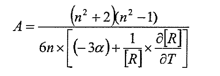


| S1 surface diffraction order | ||
| | 655nm | |
| Embodiment | ||
| 1 | second order | first order |
| Embodiment 2 | third order | second order |
| Embodiment 3 | fifth order | third order |
| Embodiment 4 | eighth order | fifth order |


| S1 Surface Diffraction Order | |
| 405nm | 655nm |
| Second Order | First Order |
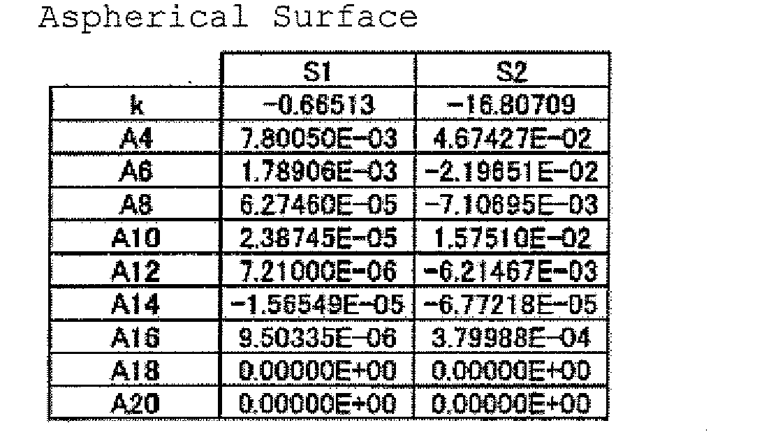
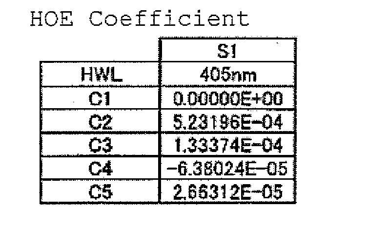


| S1 Surface diffraction Order | |
| 405nm | 655nm |
| Third Order | Second order |
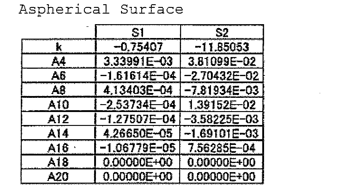
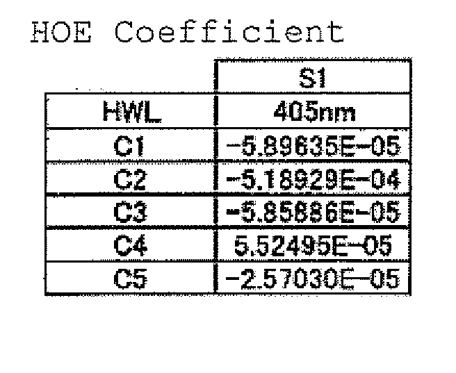
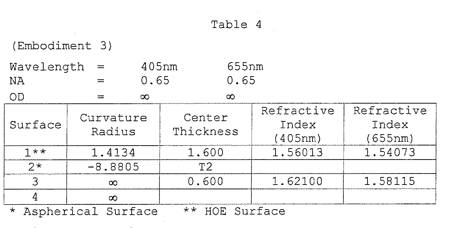

| S1 Surface diffraction Order | |
| 405nm | 655nm |
| Fifth order | Third order |
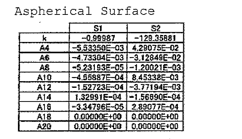
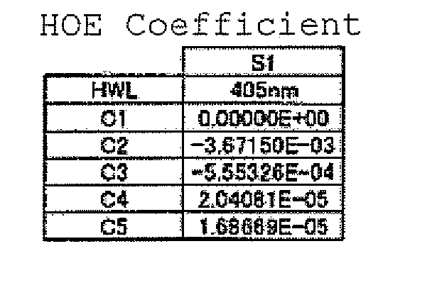
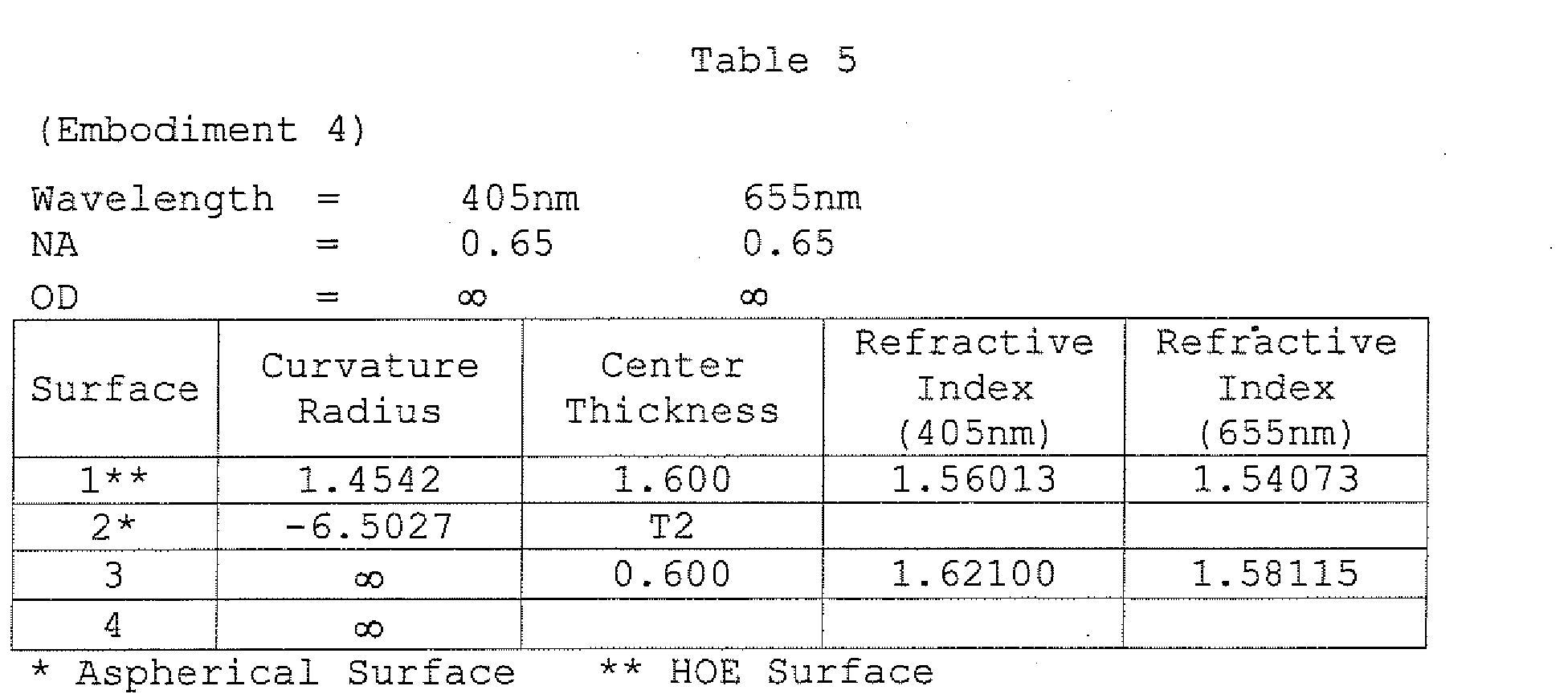

| S1 Surface diffraction Order | |
| 405nm | 655nm |
| Eighth order | Fifth order |

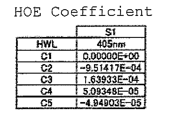


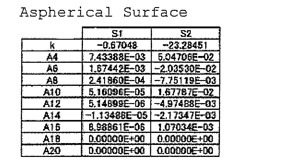
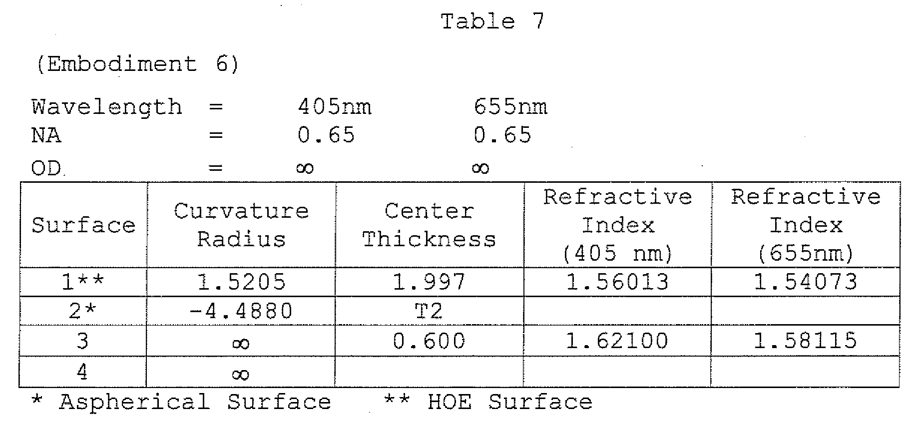

| S1 Surface diffraction Order | |
| 405nm | 655nm |
| Zero Order | First Order |

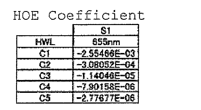
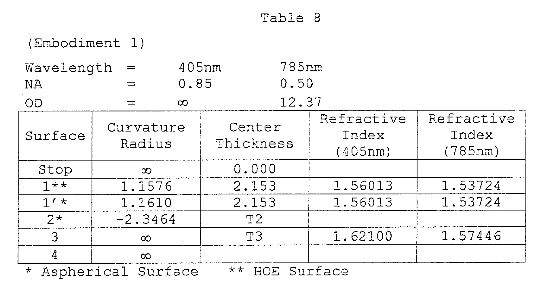

| Diffraction Order | ||
| 405nm | 785nm | |
| S1 | Second Order | First Order |
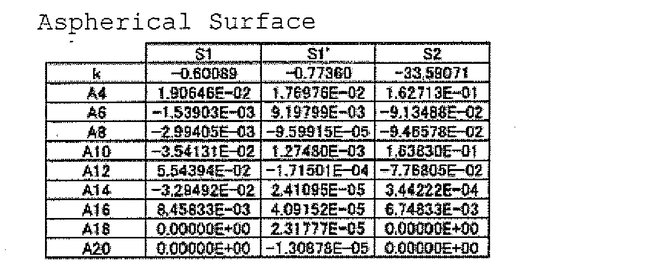
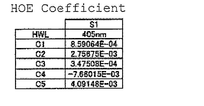
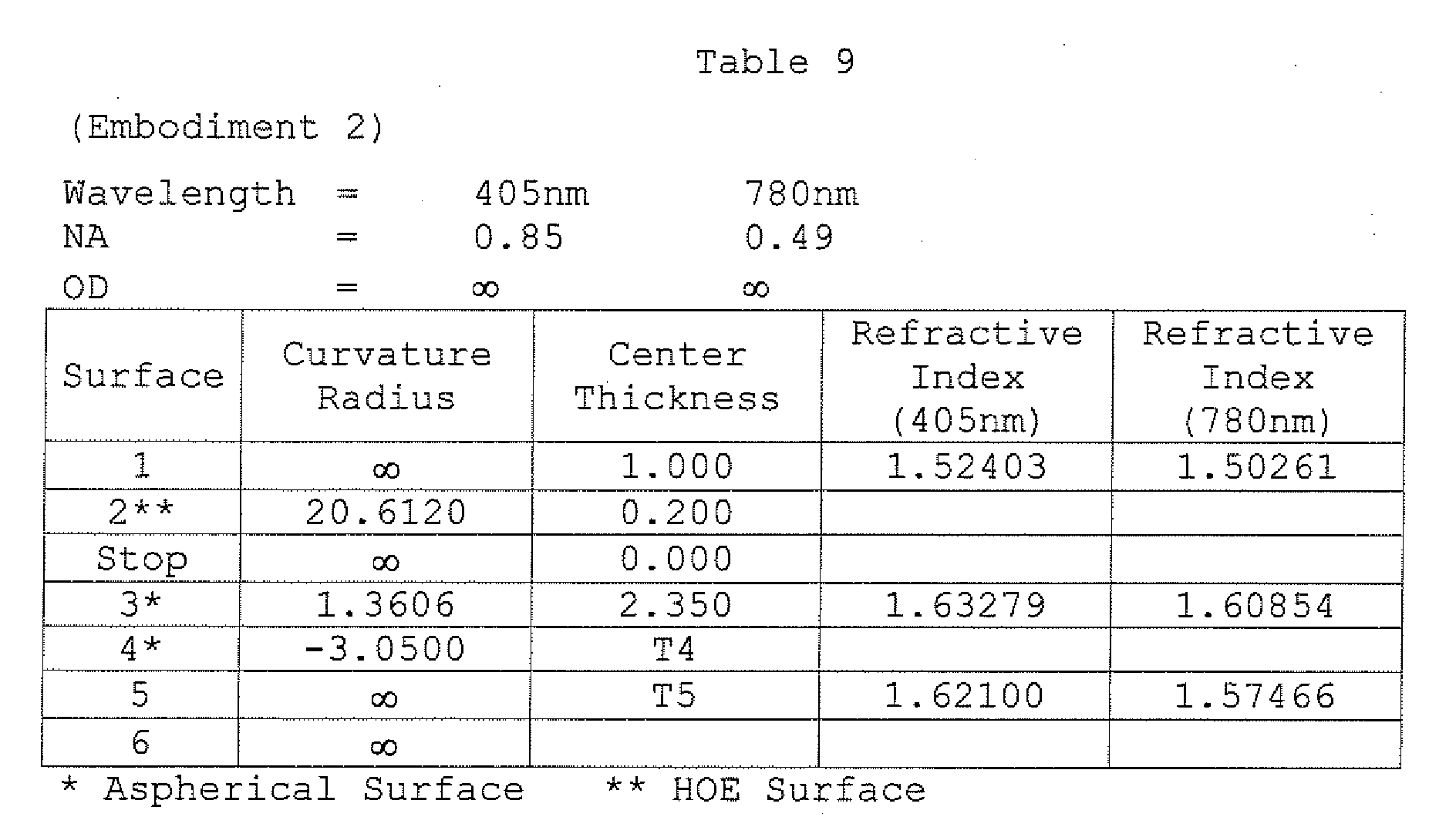

| Diffraction Order | ||
| 405nm | 780nm | |
| S2 | Zero Order | First Order |
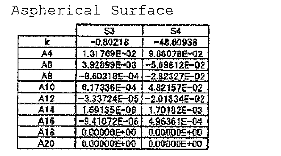
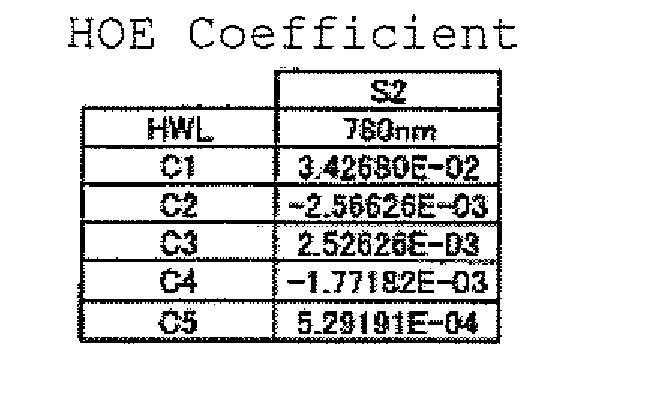

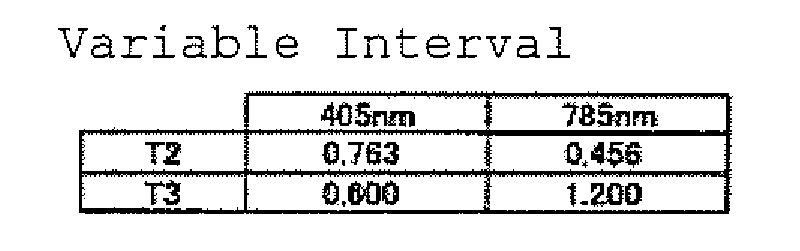
| S1 Surface Diffraction Order | |
| 405nm | 785nm |
| Second Order | First Order |

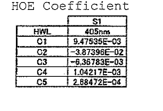
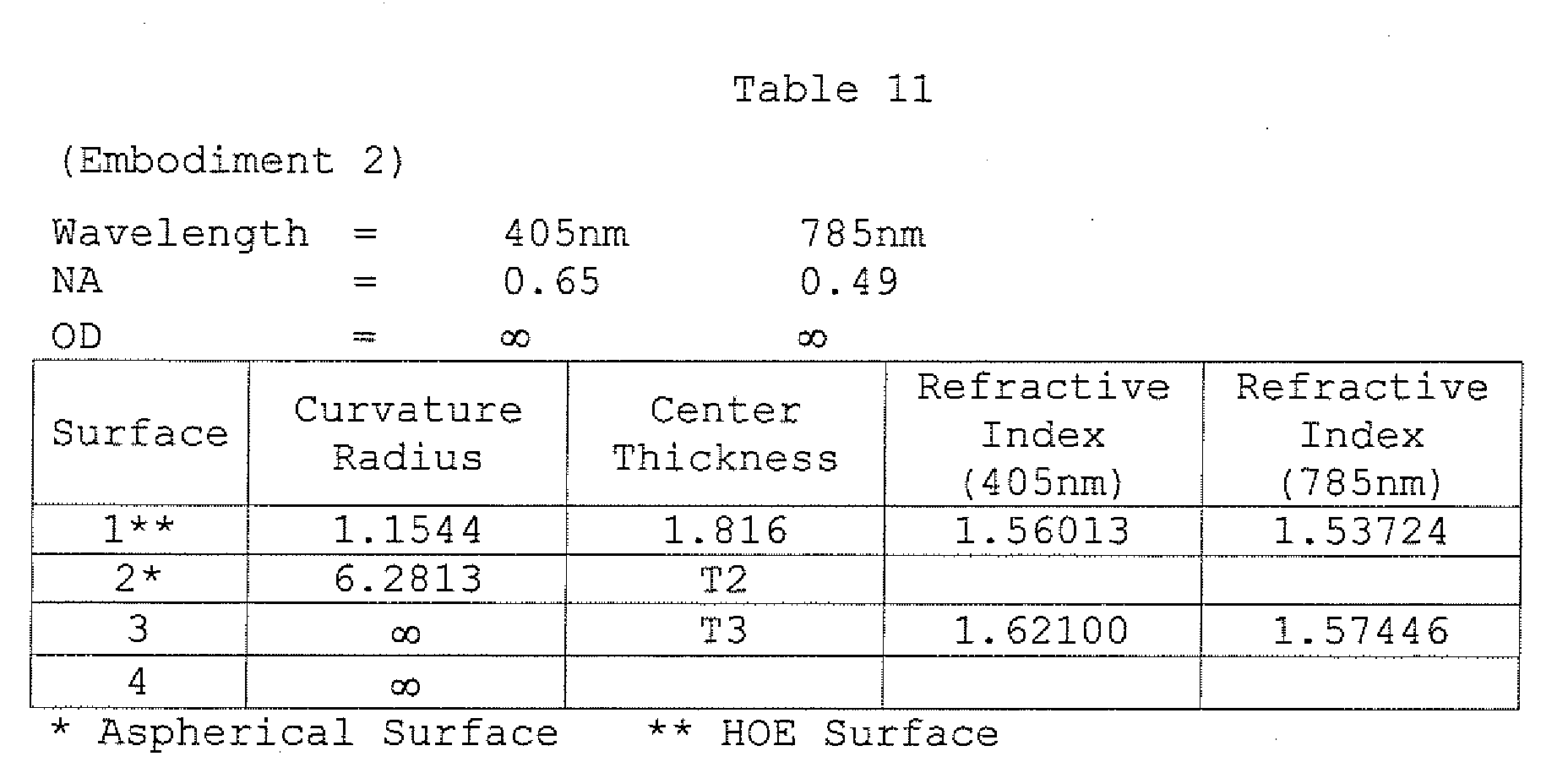
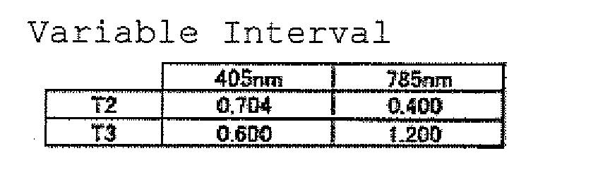
| S1 Surface Diffraction Order | |
| 405nm | 785nm |
| Second Order | First Order |
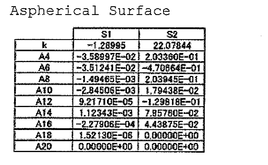
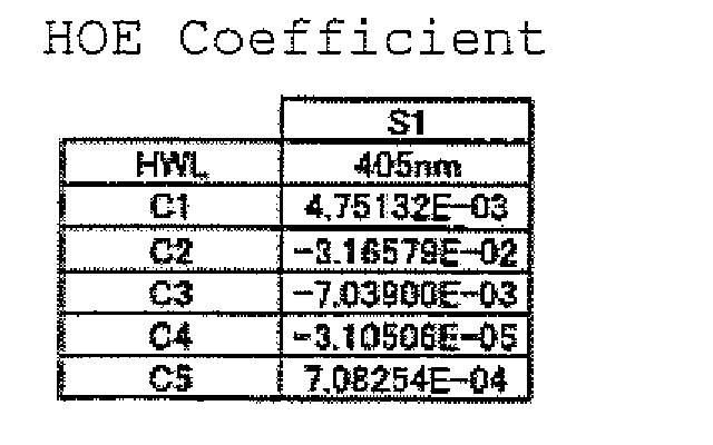
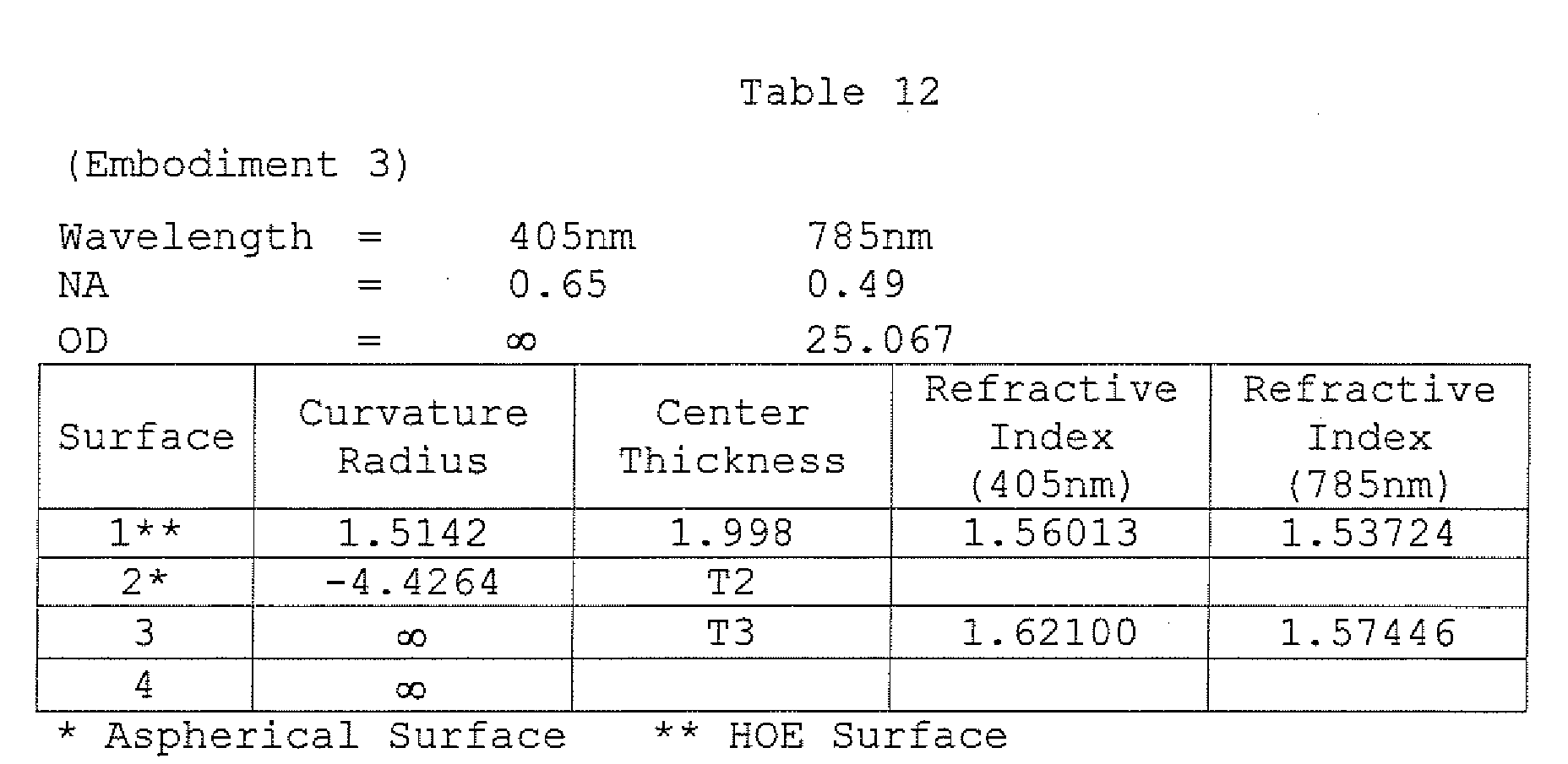
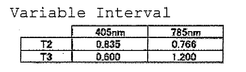
| S1 Surface Diffraction Order | |
| 405nm | 785nm |
| Zero Order | Zero Order |
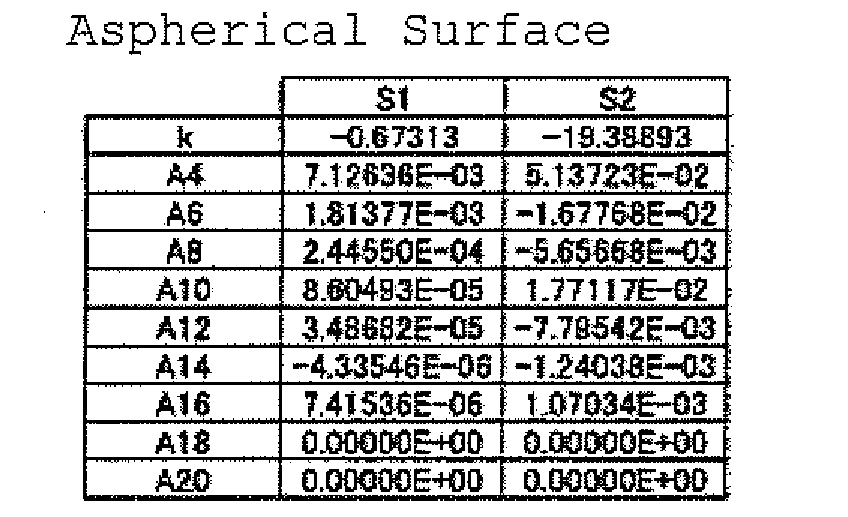
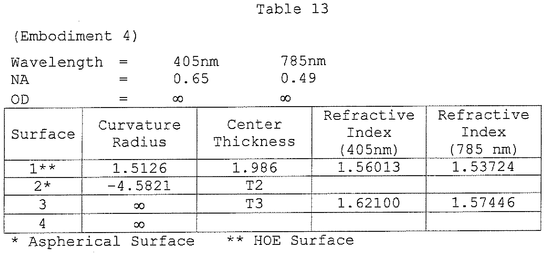

| S1 Surface Diffraction Order | |
| 405nm | 785nm |
| Zero Order | First Order |
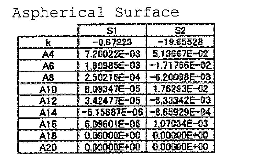
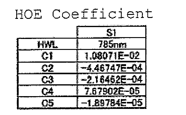
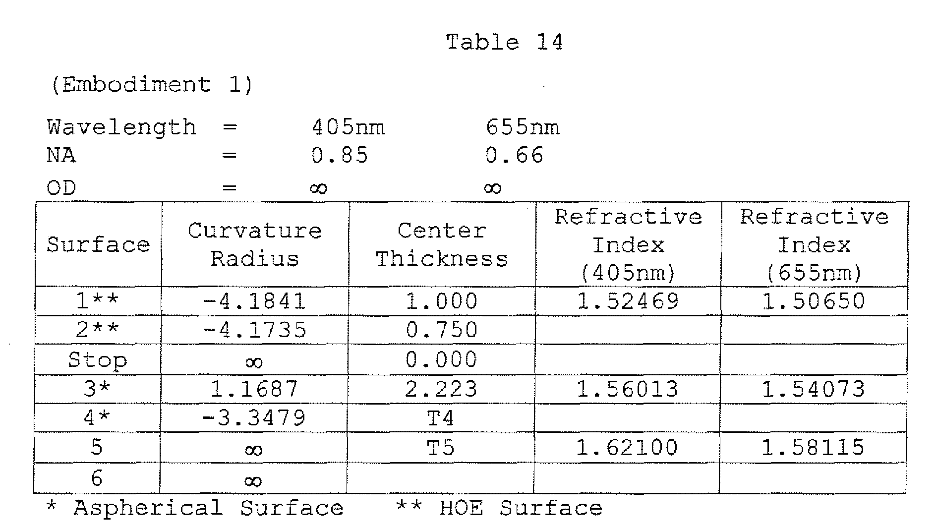

| Diffraction Order | ||
| 405nm | 655nm | |
| S1 | Zero Order | First Order |
| S2 | Zero Order | Zero Order |
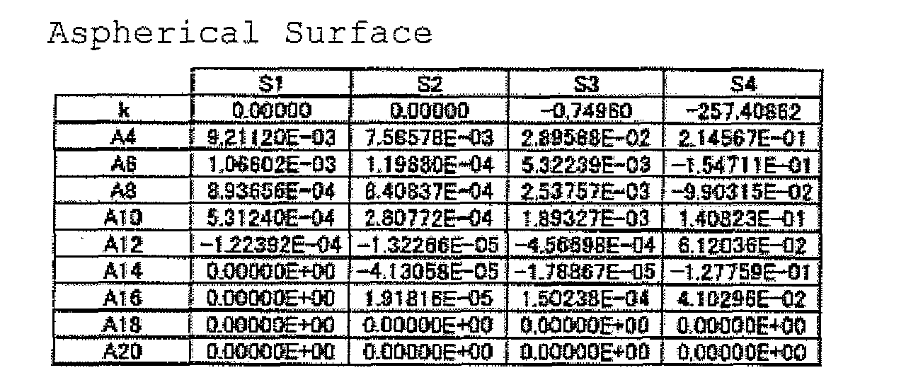
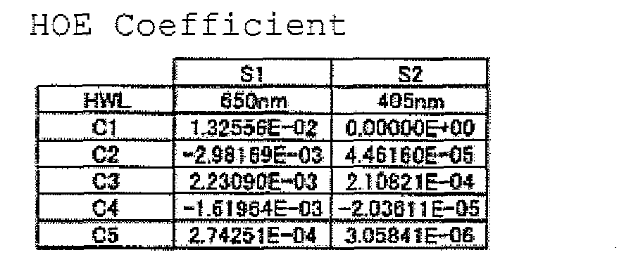
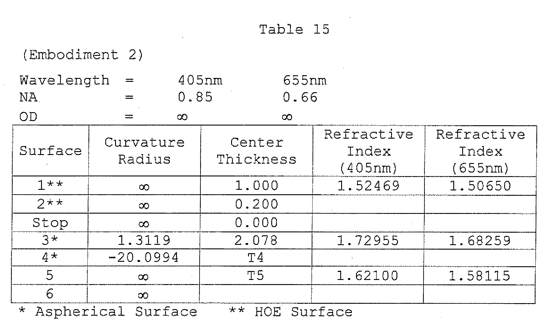
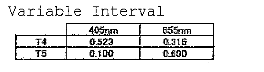
| Diffraction Order | ||
| 405nm | 655nm | |
| S1 | Zero Order | First Order |
| S2 | Zero Order | Zero Order |
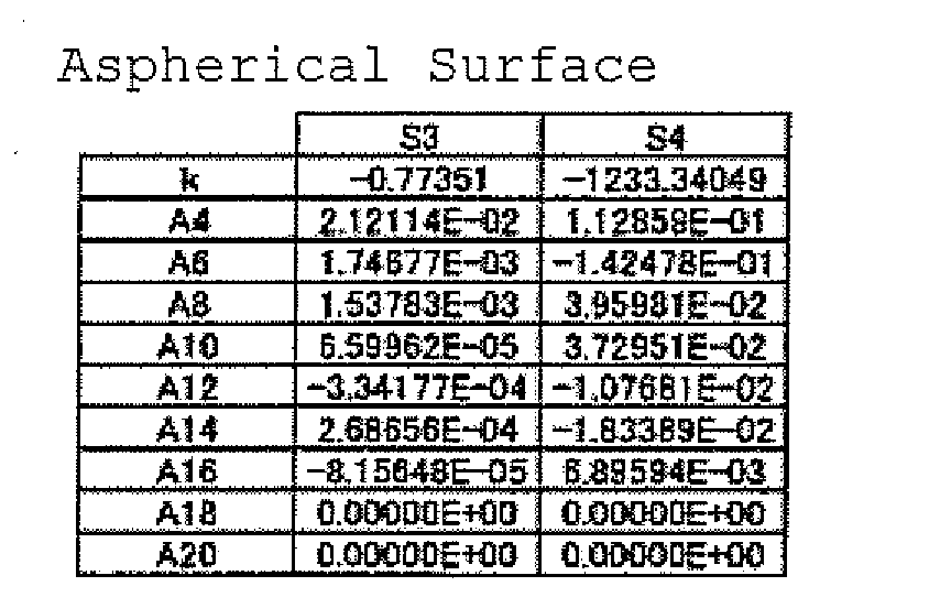
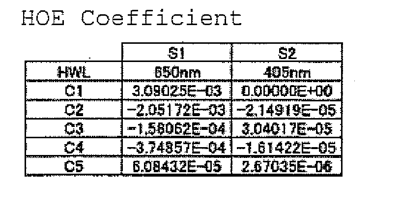
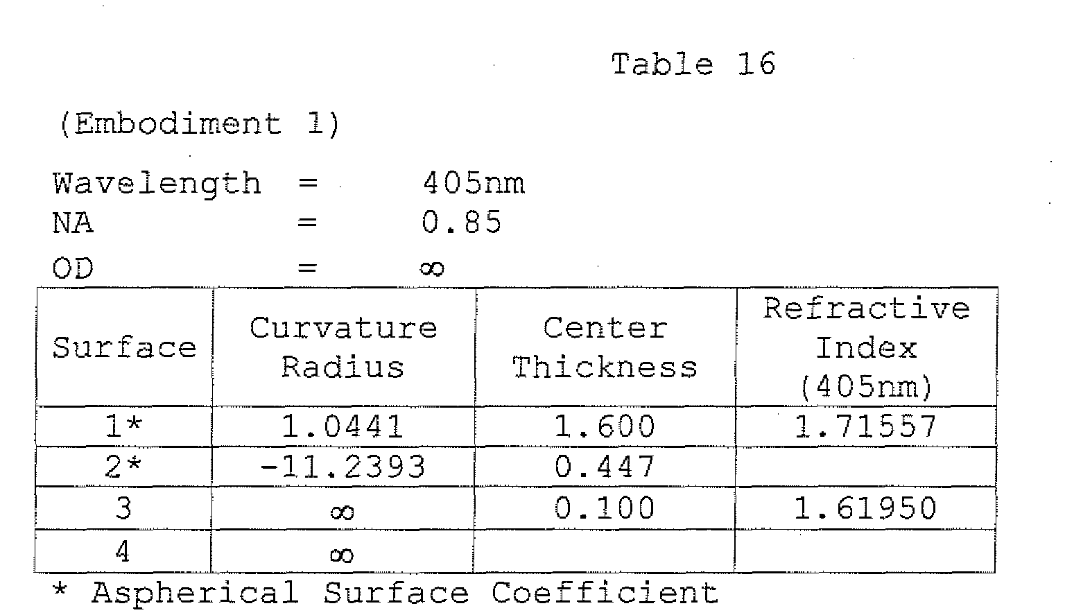
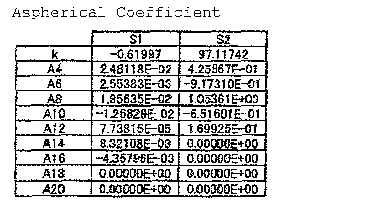
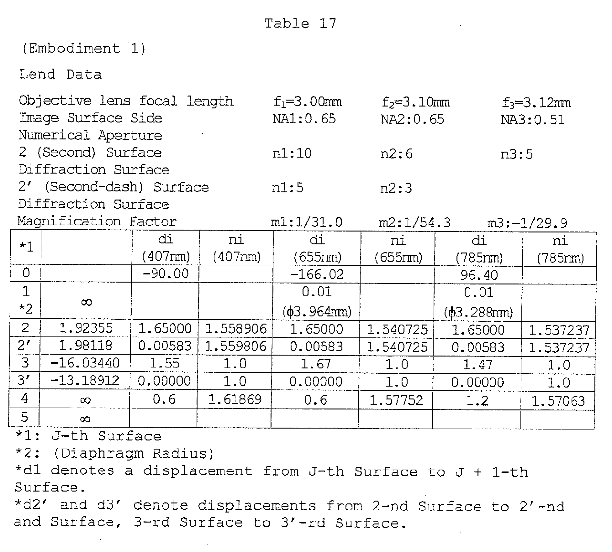
| κ | -4.4662 x E-1 | ||
| A1 | +8.7126 x E-4 | P1 | 4.0 |
| A2 | -1.9063 x E-3 | P2 | 6.0 |
| A3 | +9.2646 x E-4 | P3 | 8.0 |
| A4 | -2.1198 x E-4 | P4 | 10.0 |
| A5 | +1.6273 x E-7 | P5 | 12.0 |
| A6 | +1.3793 x E-6 | P6 | 14.0 |
| C2 | -9.6498E-05 |
| C4 | -8.3988E-06 |
| C6 | -3.1284E-06 |
| C8 | 5.6541E-07 |
| C10 | -1.7042E-07 |
(0<h<1.662 nm: HD DVD/DVD/CD common area)
| κ | -4.1961 x E-1 | ||
| A1 | +3.0725 x E-3 | P1 | 4.0 |
| A2 | -2.5861 x E-3 | P2 | 6.0 |
| A3 | +9.6551 x E-4 | P3 | 8.0 |
| A4 | -1.3826 x E-4 | P4 | 10.0 |
| A5 | +7.5482 x E-6 | P5 | 12.0 |
| A6 | -7.5795 x E-7 | P6 | 14.0 |
| C2 | -2.2814E-04 |
| C4 | -1.1010E-05 |
| C6 | -6.4735E-06 |
| C8 | -4.2984E-07 |
| C10 | 4.7450E-07 |
| κ | -8.0653 x E+2 | ||
| A1 | -5.5926 x E-3 | P1 | 4.0 |
| A2 | +1.1660 x E-2 | P2 | 6.0 |
| A3 | -6.4291 x E-3 | P3 | 8.0 |
| A4 | +1.5528 x E-3 | P4 | 10.0 |
| A5 | -1.3029 x E-4 | P5 | 12.0 |
| A6 | -3.4460 x E-6 | P6 | 14.0 |
| κ | -1.2782 x E+3 | ||
| A1 | -7.3881 x E-3 | P1 | 4.0 |
| A2 | +1.1800 x E-2 | P2 | 6.0 |
| A3 | -6.0862 x E-3 | P3 | 8.0 |
| A4 | +1.6068 x E-3 | P4 | 10.0 |
| A5 | -2.3565 x E-4 | P5 | 12.0 |
| A6 | +1.5370 x E-5 | P6 | 14.0 |
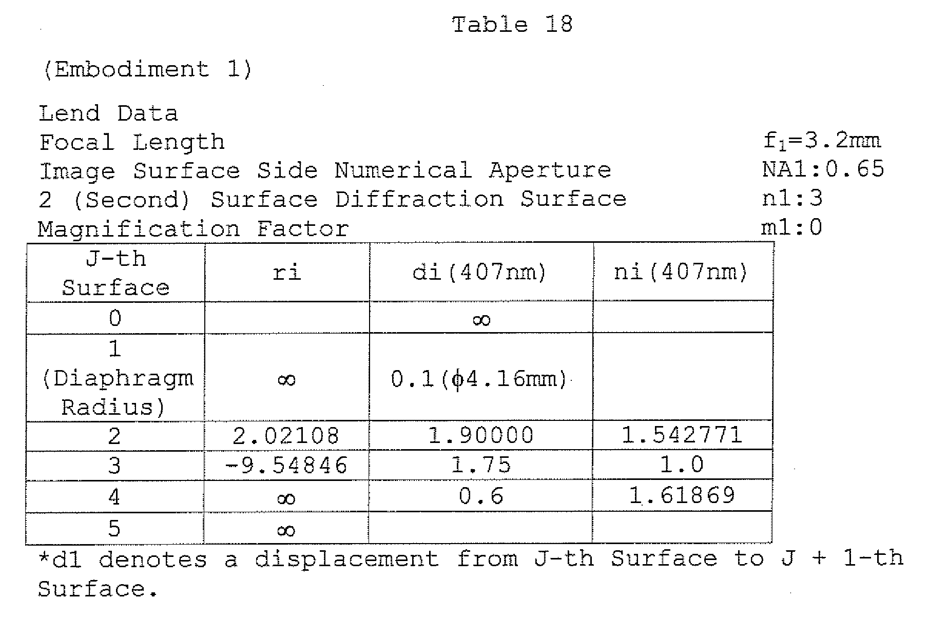
| κ | -4.4201 x E-1 | ||
| A1 | -6.6218 x E-4 | P1 | 4.0 |
| A2 | -1.4866 x E-3 | P2 | 6.0 |
| A3 | +5.2339 x E-4 | P3 | 8.0 |
| A4 | -1.0140 x E-4 | P4 | 10.0 |
| A5 | +8.5260 x E-6 | P5 | 12.0 |
| A6 | -1.1279 x E-6 | P6 | 14.0 |
| C2 | -1.0575E-03 |
| C4 | -1.1481E-04 |
| C6 | -1.1143E-04 |
| C8 | 2.1420E-05 |
| C10 | -2-1247E-06 |
| k | -1.7944 x E+2 | ||
| A1 | -9.8565 x E-3 | P1 | 4.0 |
| A2 | +1.1687 x E-2 | P2 | 6.0 |
| A3 | -5.1568 x E-3 | P3 | 8.0 |
| A4 | +1.1684 x E-3 | P4 | 10.0 |
| A5 | -1.4004 x E-4 | P5 | 12.0 |
| A6 | +7.0266 x E-6 | P6 | 14.0 |
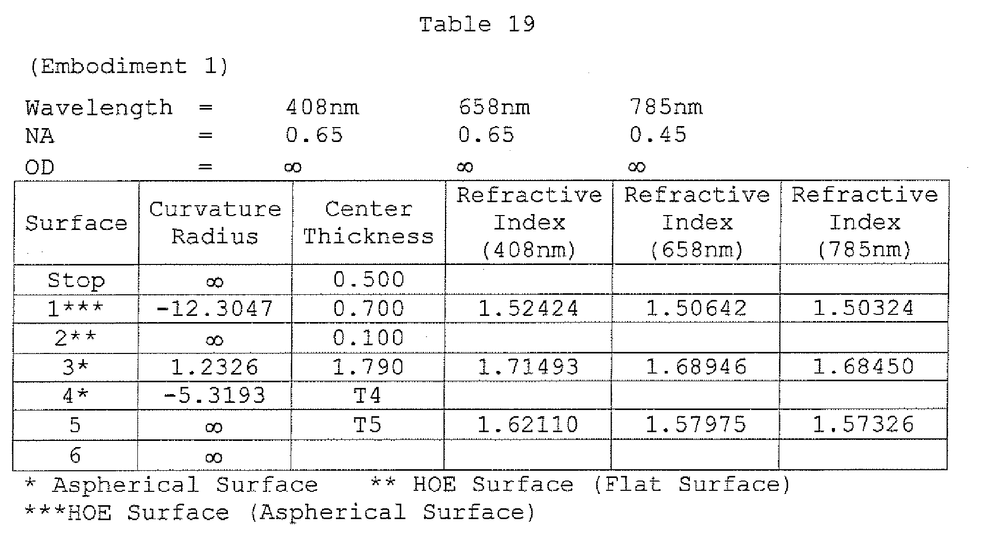
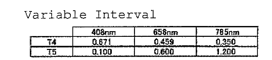
| Diffraction Order | |||
| 408nm | 658nm | 785nm | |
| S1 | Zero Order | First Order | Zero Order |
| S2 | Zero Order | Zero Order | First Order |

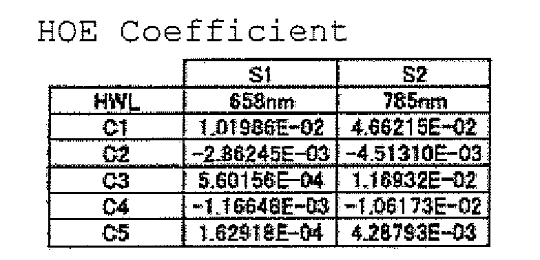
Claims (34)
- An optical pickup apparatus for recording and/or reproducing information onto or from a first optical information recording medium having a first protective layer with a thickness of t1 and second optical information recording medium having a second protective layer with a thickness of t2, where t1 # t2, by using first light beams having a wavelength λ1, the optical pickup apparatus comprising:wherein when recording and/or reproducing the information onto or from the first optical information recording medium, one of the first objective optical lens and the second objective optical lens, which are independently provided in separate bodies, is used to condense the first light beams onto a first information recording surface through the first protective layer, anda first light source for emitting first light beams having the wavelength of λ1;a first objective optical element; anda second objective optical element;
when recording and or reproducing the information onto or from the second optical information recording medium, the other one of the first objective optical lens and the second objective optical lens, is used to condense the first light beams onto a second information recording surface through the second protective layer,
wherein the first protective layer having thickness of t1 and the second protective layer having thickness of t2 satisfy a following formula, - The optical pickup apparatus of claim 1, further comprising:an objective optical element driving device to move the first objective optical element or the second objective optical element into an optical path of the first light beams emitted from the first light source to the first objective optical information medium or the second objective optical information medium, when recording and/or reproducing information onto or from the first optical information medium or the second optical information medium.
- The optical pickup apparatus of claim 1, further comprising:wherein the beam splitter is arranged to guide a part of the first light beams separated by the beam splitter to the first direction to the first objective optical element and to guide a part of the first light beams to a second direction separated by the beam splitter to the second objective optical element, while the first objective element and the second objective element are fixedly arranged, when recording and/or reproducing information onto or from the first optical information recording medium and the second optical information recording medium.a beam splitter to separate the first light beams entered into the beam splitter to a first direction and a second direction,
- The optical pickup apparatus of claim 3, further comprising:wherein the first objective optical element and the second objective optical element are fixedly arranged so that each optical axis of the first objective optical element and the second objective optical element are parallel to each other when recording and/or reproducing information onto or from the first optical information recording medium or the second optical information recording medium.a mirror for changing an optical path so as to guide a part of the first light beams separated by the beam splitter to the first direction or the second direction,
- The optical pickup apparatus of claim 1, further comprising:wherein when recording and/or reproducing information onto or from the first optical information recording medium and the second optical information recording medium and the first objective optical element and the second objective optical element are fixedly deployed,a mirror capable of moving between a first position and a second position, the mirror being placed in an optical path through which the first light beams travels to the first optical information recording medium and the second optical information recording medium,
the mirror guides the light beams to the first objective optical element, when the mirror is positioned on the first position, and
the mirror guides the light beams to the second objective optical element, when the mirror is positioned on the second position. - An optical pickup apparatus for recording and/or reproducing information onto or from a first optical information recording medium having a first protective layer with a thickness of t1 and second optical information recording medium having a second protective layer with a thickness of t2, where t1 # t2, and a third optical information recording medium having a third protective layer with a thickness of t3 having a third recording density which is different from a first recording density of the first optical information recording medium and a second recording density of the second optical information recording medium, by using at least first light beams having a wavelength λ1 and second light beams having a wavelength λ2, where λ1 # λ2, the optical pickup apparatus comprising:wherein when recording and/or reproducing the information onto or from the first optical information recording medium, one of the first objective optical lens and the second objective optical lens, which are independently provided in a separate body, is used to condense the first light beams onto a first information recording surface through the first protective layer,a first light source for emitting first light beams having the wavelength of λ1;a second light source for emitting second light beams having the wavelength λ2;a first objective optical element; anda second objective optical element;
when recording and/or reproducing the information onto or from the second optical information recording medium, the other one of the first objective optical lens and the second objective optical lens, is used to condense the first light beams onto a second information recording surface through the second protective layer, and
when recording and/or reproducing the information onto or from the third optical information recording medium, one of the first objective optical lens and the second objective optical lens is used to condense the second light beams onto a third information recording surface through the third protective layer,
wherein the first protective layer having thickness of t1 and the second protective layer having thickness of t2 satisfy a following formula, - The optical pickup apparatus of claim 6, further comprising:wherein a mirror to reflect the first light beams or the second light beams to a direction being parallel with axes of the first objective optical element and the second objective optical element is not placed in an optical path between the first and second light sources and the wavelength selection element.a wavelength selection element to selectively change an emitting direction of first light beams from the first light source and second light beams from the second light source based on a difference of wavelengths of the first beams and the second beams, the wavelength selection element being placed in a position to which both of the first light beams and the second light beams enter,
- The optical pickup apparatus of claim 6, further comprising:an objective optical element driving device to move and position the first objective optical element or the second objective optical element in an optical path through which light beams from the first light beam source to the first optical information recording medium or the second optical information recording medium pass, when recording and or reproducing information onto or from the first optical information recording medium or the second optical information recording medium.
- The optical pickup apparatus of claim 11,
wherein the first light source and the second light source are structured into a single package. - The optical pickup apparatus of claim 6,
wherein the thickness of protective layers of the second optical information medium and the third optical information medium is the same. - An optical pickup apparatus for recording and/or reproducing information onto or from a first optical information recording medium having a first protective layer with a thickness of t1 and second optical information recording medium having a second protective layer with a thickness of t2, where t1 # t2, a third optical information recording medium having a third protective layer with a thickness of t3 having a third recording density which is different from a first recording density of the first optical information recording medium and a second recording density of the second optical information recording medium, and a fourth optical recording media having a fourth protective layer with a thickness of t4, where t4 # t1, t4 # t2, by using at least first light beams having a wavelength λ1, second light beams having a wavelength λ2, where λ1 # λ2 and third light beams having a wavelength λ3, where λ1 # λ3 and λ2 # λ3, the optical pickup apparatus comprising:wherein when recording and/or reproducing the information onto or form the first optical information recording medium, one of the first objective optical lens and the second objective optical lens, which are independently provided in separate bodies, is used to condense the first light beams onto a first information recording surface through the first protective layer,a first light source for emitting first light beams having the wavelength of λ1;a second light source for emitting second light beams having the wavelength λ2;a third light source for emitting third light beams having the wavelength λ3;a first objective optical element; anda second objective optical element;
when recording and/or reproducing the information onto or from the second optical information recording medium, the other one of the first objective optical lens and the second objective optical lens, is used to condense the first light beams onto a second information recording surface through the second protective layer,
when recording and/or reproducing the information onto or from the third optical information recording medium, one of the first objective optical lens and the second objective optical lens is used to condense the second light beams onto a third information recording surface through the third protective layer, and
when recording and/or reproducing the information onto or from the fourth optical information recording medium, one of the first objective optical lens and the second objective optical lens is used to condense the third light beams onto a fourth information recording surface through the fourth protective layer,
wherein the first protective layer having thickness of t1 and the second protective layer having thickness of t2 satisfy a following formula, - The optical pickup apparatus of claim 11,
wherein one of the first objective optical element and the second objective optical element is structured by a glass lens. - The optical pickup apparatus of claim 11,
wherein one of the first objective optical element and the second objective optical element is used to record and or reproduce information onto or from the first optical information recording medium, and the other one of the first objective optical element and the second objective optical element is used to record and or reproduce information onto or from the second optical information recording medium, the third optical information recording medium and the fourth optical information recording medium. - The optical pickup apparatus of claim 11, further comprising:wherein a mirror to reflect the first light beams or the second light beams to a direction being parallel with light beam axes of the first objective optical element and the second objective optical element is not placed in an optical path between the first and second light sources and the wavelength selection element.a wavelength selection element to selectively change an emitting direction of the first light beams from the first light source and the second light beams from the second light source based on a difference of wavelengths of the first beams and the second beams,
- The optical pickup apparatus of claim 11, further comprising:an objective optical element driving device to move and position the first objective optical element or the second objective optical element in an optical path through which light beams of from the first to third light beam sources, to the first to the fourth optical information recording media pass, when recording and or reproducing information onto or from the first to the fourth optical information recording media.
- The optical pickup apparatus of claim 15,
wherein the objective optical element driving device has a lens holder for holding the first objective optical element and the second objective optical element so that each optical axis of the first objective optical element and the second objective optical element is positioned on a same circumference, and
a driving device to rotate a supporting shaft arranged in a center of the lens holder, the driving device being provided on an edge portion of the lens holder,
wherein when recording and/or reproducing information onto or from the first optical information recording medium, the first objective optical element is positioned in the optical axis by a first rotating operation of the lens holder, and
when recording and/or reproducing information onto or from the second optical information recording medium, the second objective optical element is positioned in the optical axis by a second rotating operation of the lens holder. - The optical pickup apparatus of claim 11,
wherein the first to the third light sources are structured into a single package. - The optical pickup apparatus of claim 13,
wherein the second to the third light sources are structured into a single package. - The optical pickup apparatus of claim 18, further comprising:wherein the first part of the first light beams transmitted through the half mirror are guided into the first objective optical element and the part of the first light beams reflected by the half mirror is guided into the second objective optical element,a wavelength selection element to selectively transmit or reflect the first light beams, the second light beams and the third light beams, the wavelength selection element being deployed on a first position where the first light beams from the first light source, the second light beams from the second light source and the third light beams from the third light source, the second and third light sources being packaged into a single package, are entered;a collimator to shape incident light beams of the collimator into parallel light beams, the collimator being placed on a second position where from the first to the third light beams transmitted through or reflected by the wavelength selection element are entered;a beam expander to change a diameter of at least one of the first light beams, the second light beams and the third light beams transmitted through the collimator;a quarter wave plate placed on a third position where from the first to the third light beams transmitted through the beam expander are guided together; anda half mirror having a characteristic to transmit a first part of the first light beams and reflect a part of the first light beams, and to transmit or reflect the second and third light beams, the half mirror being placed on a third position where from the first to the third light beams transmitted are entered together;
wherein the second and third light beams which are transmitted through or reflected by the half mirror are guided into the first objective optical element or the second objective optical element, and
wherein when recording and or reproducing information onto or from the first to the fourth optical information recording media, the first and the second objective optical elements are fixedly deployed. - The optical pickup apparatus of claim 18, further comprising:wherein when the mirror is deployed on the first position, the mirror guides from the first to the third light beams to the first objective optical element anda wavelength selection element to selectively transmit or reflect the first light beams, the second light beams and the third light beams, the wavelength selection element being deployed on a first position where the first light beams from the first light source, the second light beams from the second light source and the third light beams from the third light source, the second and third light sources being packaged into a single package, are entered;a collimator to shape incident light beams of the collimator into parallel light beams, the collimator being placed on a second position where from the first to the third light beams transmitted through or reflected by the wavelength selection element are entered;a beam expander to change a diameter of at least one of the first light beams, the second light beams and the third light beams transmitted through the collimator;a quarter wave plate placed on a third position where from the first to the third light beams transmitted through the beam expander are entered together; anda mirror capable of moving between a first and a second positions to reflect and guide each of the first light beams, second light beams and the third light beams to the first and second objective optical elements;
when the mirror is deployed on the second position, the mirror guides the first light beams to the second objective optical element,
wherein when recording and or reproducing information onto or from the first to the fourth optical information recording media, the first and the second objective optical elements are fixedly deployed. - The optical pickup apparatus of claim 6 or 11, further comprising:wherein the beam splitter is arranged to guide a part of the first light beams separated by the beam splitter to the first direction to the first objective optical element and to guide a part of the first light beams to a second direction separated by the beam splitter to the second objective optical element, while the first objective element and the second objective element are fixedly arranged, when recording and/or reproducing information onto or from the first optical information recording medium and the second optical information recording medium.a beam splitter capable of separating incident light beams of the beams splitter to a first direction and a second direction, the beam splitter being deployed in an optical path through which the first light beams emitted from the first light source pass,
- The optical pickup apparatus of claim 3 or 21,
wherein the beam splitter is a half mirror for separating incident light beams of the beam splitter into transmitted light beams and reflected light beams. - The optical pickup apparatus of claim 3 or 21,
wherein the beam splitter is a polarized beam splitter for separating incident light beams of the beam splitter based on a polarization element of incident light beams of the polarized beam splitter. - The optical pickup apparatus of claim 21, further comprising:wherein the first objective optical element and the second objective optical element are fixedly arranged so that each optical axis of the first objective optical element and the second objective optical element are parallel to each other when recording and/or reproducing information onto or from the first optical information recording medium or the second optical information recording medium.a mirror to change a direction of the optical path so as to guide a part of the first light beams which travel in the first direction or the second direction, which is separated by the beam splitter to the first objective optical element or the second objective optical element,
- An optical pickup apparatus for recording and/or reproducing information onto or from a first optical information recording medium having a first protective layer with a thickness of t1 and a second optical information recording medium having a second protective layer with a thickness of t2, where t1 ≠ t2, a third optical information recording medium having a third protective layer with a thickness of t3 having a third recording density which is different from a first recording density of the first optical information recording medium and a second recording density of the second optical information recording medium, and a fourth optical recording media having a fourth protective layer with a thickness of t4, where t4 ≠ t1, t4 ≠ t2, by using at least first light beams having a wavelength λ1, where 400 nm ≤ λ1 ≤ 420 nm, second light beams having a wavelength λ2, where 640 nm ≤ λ2 ≤ 670 nm and third light beams having a wavelength λ3, where 780 nm ≤ λ3 ≤ 800 nm, the optical pickup apparatus comprising:wherein when recording and/or reproducing the information onto or from the first optical information recording medium, the first objective optical lens is used to condense the first light beams onto a first information recording surface through the first protective layer,a first light source for emitting first light beams having the wavelength of λ1;a second light source for emitting second light beams having the wavelength λ2;a third light source for emitting third light beams having the wavelength λ3;a first objective optical element; anda second objective optical element;
when recording and or reproducing the information onto or from the second optical information recording medium, the second objective optical lens is used to condense the first light beams onto a second information recording surface through the second protective layer,
when recording and or reproducing the information onto or from the third optical information recording medium, the second objective optical lens is used to condense the second light beams onto a third information recording surface through the third protective layer, and
when recording and or reproducing the information onto or from the fourth optical information recording medium, the second objective optical lens is used to condense the third light beams onto a fourth information recording surface through the fourth protective layer,
wherein the first protective layer having thickness of t1 and the second protective layer having thickness of t2 satisfy a following formula,
a first area through which a center light beam portion of the first, the second and the third light beams including an optical axis of the second objective optical lens pass, and
a second area through which optical beams of an outer side of the center light beam portion pass,
to condense the first light beams passing through the first area and the second area onto or from the second optical information recording medium, when recording and/or reproducing information onto or from the second optical information recording medium,
to condense the second light beams passing through the first area and the second area onto or from the third optical information recording medium, when recording and/or reproducing information onto or from the third optical information recording medium, and
to condense the third light beams passing through the first area onto or from the fourth optical information recording medium, when recording and/or reproducing information onto or from the fourth optical information recording medium. - The optical pickup apparatus of claim 25,
wherein the second objective optical element includes a first diffraction structure in the first area, and a second diffraction structure being different from the first diffraction structure in the second area,
wherein the first and the second light beams enter into the second objective optical element as converging light beams and the third light beams enter into the second objective optical element as diverging light beams. - The optical pickup apparatus of claim 25,
wherein the second objective optical element diffracts from the first to the third light beams entered into the first diffraction structure as tenth order, sixth order and fifth order diffraction light beams and diffracts from the first to the second light beams as fifth order and third order diffraction light beams. - The optical pickup apparatus of claim 19 or 20,
wherein the collimator comprises a step difference structure to correct chromatic aberration which occurs with at least one of the first objective optical element and the second objective optical element. - The optical pickup apparatus of claim 20 or 21,
wherein the beam expander corrects at least one of spherical aberration caused by the differences of protective layers of from the first to the fourth optical information recording media,
chromatic aberration or spherical aberration caused by wavelength drift or wavelength switching, and
spherical aberration caused by temperature drift. - The optical pickup apparatus of claim 20 or 21,
wherein the beam expander comprises plural optical elements and at least one of the plural optical elements is capable of moving in a optical axis direction of the beam expander. - The optical pickup apparatus of claim 20 or 21,
wherein the beam expander contains an optical element having an optical surface on which plural step difference structures to correct the chromatic aberration. - The optical pickup apparatus of claim 1, 6, 11 or 25,
wherein at lease one of the first objective optical element and the second objective optical element is structured by plastic material and is a single optical element having a phase structure thereon. - The optical pickup apparatus of claim 1, 6, 11 or 25,
wherein at least one of the first objective optical element and the second objective optical element includes a first optical element and a second optical element, and at least one of the first optical element and the second optical element is structured by plastic. - The optical pickup apparatus of claim 1, 6, 11 or 25,
wherein at least one of the first objective optical element and the second objective optical element includes a first optical element and a second optical element, and at least one of the first optical element and the second optical element is structured by plastic and the other one of the first optical element and the second optical element has a phase structure thereon.
Applications Claiming Priority (2)
| Application Number | Priority Date | Filing Date | Title |
|---|---|---|---|
| JP2004140311 | 2004-05-10 | ||
| JP2004140311 | 2004-05-10 |
Publications (2)
| Publication Number | Publication Date |
|---|---|
| EP1596383A2 true EP1596383A2 (en) | 2005-11-16 |
| EP1596383A3 EP1596383A3 (en) | 2007-11-07 |
Family
ID=34939721
Family Applications (1)
| Application Number | Title | Priority Date | Filing Date |
|---|---|---|---|
| EP05103784A Withdrawn EP1596383A3 (en) | 2004-05-10 | 2005-05-06 | Optical pickup apparatus |
Country Status (5)
| Country | Link |
|---|---|
| US (1) | US20050249097A1 (en) |
| EP (1) | EP1596383A3 (en) |
| KR (1) | KR20060047697A (en) |
| CN (1) | CN100419878C (en) |
| TW (1) | TW200540857A (en) |
Cited By (3)
| Publication number | Priority date | Publication date | Assignee | Title |
|---|---|---|---|---|
| EP1615212A2 (en) * | 2004-07-09 | 2006-01-11 | Sony Corporation | Optical pickup device, recorder and/or reproducer |
| EP1840891A2 (en) * | 2006-03-30 | 2007-10-03 | Toshiba Samsung Storage Technology Corporation | Optical pickup device and optical information recording/reproducing device |
| EP1990801A1 (en) * | 2006-03-07 | 2008-11-12 | Konica Minolta Opto, Inc. | Optical pickup device, objective optical element, and optical information recording/reproducing device |
Families Citing this family (13)
| Publication number | Priority date | Publication date | Assignee | Title |
|---|---|---|---|---|
| JP2006018948A (en) * | 2004-07-02 | 2006-01-19 | Ricoh Co Ltd | Device for correcting spherical aberration, and optical pickup device |
| US7352517B2 (en) * | 2005-05-09 | 2008-04-01 | Konica Minolta Opto, Inc. | Optical pickup apparatus |
| JP2007004875A (en) * | 2005-06-22 | 2007-01-11 | Sony Corp | Optical pickup |
| JP2007052858A (en) * | 2005-08-18 | 2007-03-01 | Fujitsu Ltd | Optical disk drive |
| US8130624B2 (en) * | 2005-09-30 | 2012-03-06 | Panasonic Corporation | Optical head device for forming light spot on disc-shaped information medium |
| WO2007091184A1 (en) * | 2006-02-06 | 2007-08-16 | Koninklijke Philips Electronics N.V. | Optical pick-up unit for use in a multi-disc optical player |
| CN101034569B (en) * | 2006-03-07 | 2011-06-22 | 柯尼卡美能达精密光学株式会社 | Optical pickup apparatus, objective optical element and optical information recording reproducing apparatus |
| JP2007265585A (en) * | 2006-03-30 | 2007-10-11 | Konica Minolta Opto Inc | Optical pickup device |
| US20080019232A1 (en) * | 2006-07-21 | 2008-01-24 | Samsung Electronics Co., Ltd. | Object lens and optical pick-up device having the same |
| WO2008146675A1 (en) * | 2007-05-31 | 2008-12-04 | Konica Minolta Opto, Inc. | Objective optical element for optical pickup device and optical pickup device |
| US8300513B2 (en) * | 2007-09-26 | 2012-10-30 | Panasonic Corporation | Optical head, optical head manufacturing method and optical disc device |
| JP2009129483A (en) * | 2007-11-20 | 2009-06-11 | Sanyo Electric Co Ltd | Optical pickup device |
| KR101309704B1 (en) * | 2009-08-19 | 2013-09-17 | 도시바삼성스토리지테크놀러지코리아 주식회사 | Optical pickup device |
Citations (10)
| Publication number | Priority date | Publication date | Assignee | Title |
|---|---|---|---|---|
| GB2313700A (en) * | 1996-05-31 | 1997-12-03 | Daewoo Electronics Co Ltd | Dual beam, dual focus optical pickup |
| US6370104B1 (en) * | 1999-04-13 | 2002-04-09 | Industrial Technology Research Institute | DVD reading-writing pick-up head employing multiple wavelengths |
| US6442124B1 (en) * | 1998-03-14 | 2002-08-27 | Samsung Electronics Co., Ltd. | Compatible optical pick-up apparatus for recording and reproducing information from recording media having different formats |
| WO2002082437A1 (en) * | 2001-04-05 | 2002-10-17 | Koninklijke Philips Electronics N.V. | Optical scanning device |
| US20030048715A1 (en) * | 1998-04-04 | 2003-03-13 | Lg Electronics, Inc. | Optical pickup and optical recording/reproducing apparatus using the same |
| US20030137919A1 (en) * | 1996-08-19 | 2003-07-24 | Shinro Inui | Objective lens driving device and optical disc apparatus using the same |
| US20040047269A1 (en) * | 2002-09-05 | 2004-03-11 | Konica Corporation | Optical pickup apparatus and optical element |
| US20040052509A1 (en) * | 2002-09-13 | 2004-03-18 | Hitachi, Ltd. | Optical pick-up device and optical disk apparatus |
| EP1465171A2 (en) * | 2003-03-31 | 2004-10-06 | Konica Minolta Holdings, Inc. | Optical pickup device and objective lens for the optical pickup device |
| EP1471514A2 (en) * | 2003-04-22 | 2004-10-27 | Konica Minolta Opto, Inc. | Optical pickup device, optical information recording and reproducing apparatus, expander lens, coupling lens and chromatic aberration correcting optical element |
Family Cites Families (3)
| Publication number | Priority date | Publication date | Assignee | Title |
|---|---|---|---|---|
| JPH09179020A (en) * | 1995-08-28 | 1997-07-11 | Asahi Optical Co Ltd | Diffracting multifocal objective for optical information recording and reproducing device |
| JPH09288835A (en) * | 1996-02-23 | 1997-11-04 | Matsushita Electric Ind Co Ltd | Objective lens driving device |
| JP3517223B2 (en) * | 2001-04-24 | 2004-04-12 | 株式会社東芝 | Optical disk apparatus and optical disk processing method |
-
2005
- 2005-05-03 TW TW094114257A patent/TW200540857A/en unknown
- 2005-05-03 KR KR1020050036908A patent/KR20060047697A/en not_active Application Discontinuation
- 2005-05-05 US US11/122,003 patent/US20050249097A1/en not_active Abandoned
- 2005-05-06 EP EP05103784A patent/EP1596383A3/en not_active Withdrawn
- 2005-05-09 CN CNB2005100704617A patent/CN100419878C/en not_active Expired - Fee Related
Patent Citations (10)
| Publication number | Priority date | Publication date | Assignee | Title |
|---|---|---|---|---|
| GB2313700A (en) * | 1996-05-31 | 1997-12-03 | Daewoo Electronics Co Ltd | Dual beam, dual focus optical pickup |
| US20030137919A1 (en) * | 1996-08-19 | 2003-07-24 | Shinro Inui | Objective lens driving device and optical disc apparatus using the same |
| US6442124B1 (en) * | 1998-03-14 | 2002-08-27 | Samsung Electronics Co., Ltd. | Compatible optical pick-up apparatus for recording and reproducing information from recording media having different formats |
| US20030048715A1 (en) * | 1998-04-04 | 2003-03-13 | Lg Electronics, Inc. | Optical pickup and optical recording/reproducing apparatus using the same |
| US6370104B1 (en) * | 1999-04-13 | 2002-04-09 | Industrial Technology Research Institute | DVD reading-writing pick-up head employing multiple wavelengths |
| WO2002082437A1 (en) * | 2001-04-05 | 2002-10-17 | Koninklijke Philips Electronics N.V. | Optical scanning device |
| US20040047269A1 (en) * | 2002-09-05 | 2004-03-11 | Konica Corporation | Optical pickup apparatus and optical element |
| US20040052509A1 (en) * | 2002-09-13 | 2004-03-18 | Hitachi, Ltd. | Optical pick-up device and optical disk apparatus |
| EP1465171A2 (en) * | 2003-03-31 | 2004-10-06 | Konica Minolta Holdings, Inc. | Optical pickup device and objective lens for the optical pickup device |
| EP1471514A2 (en) * | 2003-04-22 | 2004-10-27 | Konica Minolta Opto, Inc. | Optical pickup device, optical information recording and reproducing apparatus, expander lens, coupling lens and chromatic aberration correcting optical element |
Cited By (18)
| Publication number | Priority date | Publication date | Assignee | Title |
|---|---|---|---|---|
| EP1615212A2 (en) * | 2004-07-09 | 2006-01-11 | Sony Corporation | Optical pickup device, recorder and/or reproducer |
| EP1615212A3 (en) * | 2004-07-09 | 2007-05-02 | Sony Corporation | Optical pickup device, recorder and/or reproducer |
| US7636293B2 (en) | 2004-07-09 | 2009-12-22 | Sony Corporation | Optical pickup device, recorder and/or reproducer |
| EP1990801A1 (en) * | 2006-03-07 | 2008-11-12 | Konica Minolta Opto, Inc. | Optical pickup device, objective optical element, and optical information recording/reproducing device |
| EP2001020A4 (en) * | 2006-03-07 | 2009-04-29 | Konica Minolta Opto Inc | Optical pickup apparatus, objective optical element, and optical information recording and reproducing apparatus |
| EP1993094A1 (en) * | 2006-03-07 | 2008-11-19 | Konica Minolta Opto, Inc. | Optical pickup device, objective optical element, and optical information recording/reproducing device |
| EP1993093A1 (en) * | 2006-03-07 | 2008-11-19 | Konica Minolta Opto, Inc. | Optical pickup apparatus, objective optical element, and optical information recording and reproducing apparatus |
| EP2001020A2 (en) * | 2006-03-07 | 2008-12-10 | Konica Minolta Opto, Inc. | Optical pickup apparatus, objective optical element, and optical information recording and reproducing apparatus |
| EP1993093A4 (en) * | 2006-03-07 | 2009-04-22 | Konica Minolta Opto Inc | Optical pickup apparatus, objective optical element, and optical information recording and reproducing apparatus |
| EP1990801A4 (en) * | 2006-03-07 | 2009-04-29 | Konica Minolta Opto Inc | Optical pickup device, objective optical element, and optical information recording/reproducing device |
| US7948857B2 (en) | 2006-03-07 | 2011-05-24 | Konica Minolta Opto, Inc. | Optical pickup apparatus, objective optical element and optical information recording reproducing apparatus |
| EP1993094A4 (en) * | 2006-03-07 | 2009-05-06 | Konica Minolta Opto Inc | Optical pickup device, objective optical element, and optical information recording/reproducing device |
| US7843793B2 (en) | 2006-03-07 | 2010-11-30 | Konica Minolta Opto, Inc. | Optical pickup apparatus, objective optical element and optical information recording reproducing apparatus |
| US7656770B2 (en) | 2006-03-07 | 2010-02-02 | Konica Minolta Opto, Inc. | Optical pickup apparatus, objective optical element and optical information recording reproducing apparatus |
| US7672212B2 (en) | 2006-03-07 | 2010-03-02 | Konica Minolta Opto, Inc. | Optical pickup apparatus, objective optical element and optical information recording reproducing apparatus |
| US7672211B2 (en) | 2006-03-07 | 2010-03-02 | Konica Minolta Opto, Inc. | Optical pickup apparatus, objective optical element and optical information recording reproducing apparatus |
| EP1840891A2 (en) * | 2006-03-30 | 2007-10-03 | Toshiba Samsung Storage Technology Corporation | Optical pickup device and optical information recording/reproducing device |
| EP1840891A3 (en) * | 2006-03-30 | 2007-12-19 | Toshiba Samsung Storage Technology Corporation | Optical pickup device and optical information recording/reproducing device |
Also Published As
| Publication number | Publication date |
|---|---|
| KR20060047697A (en) | 2006-05-18 |
| CN1707649A (en) | 2005-12-14 |
| US20050249097A1 (en) | 2005-11-10 |
| TW200540857A (en) | 2005-12-16 |
| CN100419878C (en) | 2008-09-17 |
| EP1596383A3 (en) | 2007-11-07 |
Similar Documents
| Publication | Publication Date | Title |
|---|---|---|
| EP1596383A2 (en) | Optical pickup apparatus | |
| JP3794229B2 (en) | OPTICAL PICKUP DEVICE, RECORDING / REPRODUCING DEVICE EQUIPPED WITH THE OPTICAL PICKUP DEVICE, INFORMATION RECORDING / REPRODUCING METHOD, AND OBJECTIVE LENS FOR OPTICAL PICKUP DEVICE | |
| EP1202259A2 (en) | Objective lens, light converging optical system, optical pickup apparatus, and recording/reproducing apparatus | |
| US20090262635A1 (en) | Objective optical system for optical pickup apparatus, optical pickup apparatus, driving apparatus for optical information recording medium, condenser lens and optical path compounding element | |
| US7889618B2 (en) | Objective optical element and optical pickup apparatus | |
| JP3859416B2 (en) | Objective lens, optical head and optical disk apparatus using the same | |
| US7352517B2 (en) | Optical pickup apparatus | |
| JP2005353261A (en) | Optical pickup device | |
| US7664003B2 (en) | Objective lens and optical pickup apparatus | |
| JP4595184B2 (en) | Optical pickup device and objective lens | |
| US8098562B2 (en) | Objective lens comprising a diffraction structure for distributing light in to light of different diffraction orders, optical pickup device, and optical information recording or reproduction apparatus having same | |
| JPWO2005074388A1 (en) | Optical pickup device and optical information recording and / or reproducing device | |
| US6728172B2 (en) | Objective lens and optical pickup apparatus | |
| US20050168821A1 (en) | Diffractive optical element and optical pickup apparatus | |
| JP3864755B2 (en) | Objective lens for optical pickup device and optical pickup device | |
| KR100767148B1 (en) | Optical Pick-Up Device and Objective Lens Therefor | |
| JP2011165224A (en) | Optical pickup and optical disk device, computer, optical disk player, optical disk recorder | |
| JP3804826B2 (en) | Objective lens for optical pickup device and optical pickup device | |
| JPWO2005088625A1 (en) | Objective optical element and optical pickup device | |
| JP4329031B2 (en) | Optical pickup device | |
| US8493831B2 (en) | Compatible optical pickup and optical recording and/or reproducing apparatus employing the same | |
| JP4400326B2 (en) | Optical pickup optical system, optical pickup device, and optical disk drive device | |
| EP1569212A2 (en) | Objective optical system, optical pickup apparatus and optical information recording and reproducing apparatus | |
| JP2004006005A (en) | Optical pickup device | |
| JP2010198717A (en) | Objective lens, optical pickup and optical disk device |
Legal Events
| Date | Code | Title | Description |
|---|---|---|---|
| PUAI | Public reference made under article 153(3) epc to a published international application that has entered the european phase |
Free format text: ORIGINAL CODE: 0009012 |
|
| AK | Designated contracting states |
Kind code of ref document: A2 Designated state(s): AT BE BG CH CY CZ DE DK EE ES FI FR GB GR HU IE IS IT LI LT LU MC NL PL PT RO SE SI SK TR |
|
| AX | Request for extension of the european patent |
Extension state: AL BA HR LV MK YU |
|
| PUAL | Search report despatched |
Free format text: ORIGINAL CODE: 0009013 |
|
| AK | Designated contracting states |
Kind code of ref document: A3 Designated state(s): AT BE BG CH CY CZ DE DK EE ES FI FR GB GR HU IE IS IT LI LT LU MC NL PL PT RO SE SI SK TR |
|
| AX | Request for extension of the european patent |
Extension state: AL BA HR LV MK YU |
|
| 17P | Request for examination filed |
Effective date: 20080507 |
|
| AKX | Designation fees paid |
Designated state(s): AT BE BG CH CY CZ DE DK EE ES FI FR GB GR HU IE IS IT LI LT LU MC NL PL PT RO SE SI SK TR |
|
| AXX | Extension fees paid |
Extension state: MK Payment date: 20080507 Extension state: LV Payment date: 20080507 Extension state: HR Payment date: 20080507 Extension state: BA Payment date: 20080507 Extension state: AL Payment date: 20080507 |
|
| 17Q | First examination report despatched |
Effective date: 20080704 |
|
| STAA | Information on the status of an ep patent application or granted ep patent |
Free format text: STATUS: THE APPLICATION IS DEEMED TO BE WITHDRAWN |
|
| 18D | Application deemed to be withdrawn |
Effective date: 20081115 |